a single dc source fed cascaded multilevel inverter … · 2018-12-17 · a single dc source fed...
TRANSCRIPT

A SINGLE DC SOURCE FED CASCADED MULTILEVEL
INVERTER WITH AC L-C-L RESONANT CONVERTER
FOR HIGH CURRENT AND LOW VOLTAGE
APPLICATIONS
A THESIS SUBMITTED IN PARTIAL FULFILLMENT OF THE REQUIREMENTS FOR THE DEGREE OF
Master of Technology
in
ELECTRICAL ENGINEERING
BY
POLU MADHAVA REDDY
ROLL NO: 213EE4325
Under the Supervision of
Prof. (Dr.) A.K.PANDA
Department of Electrical Engineering
National Institute of Technology, Rourkela-769008
2015

A SINGLE DC SOURCE FED CASCADED MULTILEVEL
INVERTER WITH AC L-C-L RESONANT CONVERTER
FOR HIGH CURRENT AND LOW VOLTAGE
APPLICATIONS
Polu Madhava Reddy
Department of Electrical Engineering
National Institute of Technology, Rourkela

Department of Electrical Engineering
National Institute of Technology Rourkela
Certificate
This is to certify that the work in the thesis entitled “ Single DC Source fed
Cascaded Multilevel inverter along with AC L-C-L Resonant converter for high
current and low voltage applications” by POLU MADHAVA REDDY is a
record of an original research work carried out by him under my supervision and guidance
in partial fulfillment of the requirements for the award of the degree of Master of
Technology with the specialization of Power electronics & Drives in the department
of Electrical Engineering, National Institute of Technology Rourkela. Neither this
thesis nor any part of it has been submitted for any degree or academic award elsewhere.
Place: NIT Rourkela Prof. A . K . P a n d a
Date: May 2015 Department of Electrical Engineering
National Institute of Technology
Rourkela – 769008
Email: [email protected]

Acknowledgment
First and Foremost, I would like to express my sincere gratitude towards my
supervisor and Head, Department of Electrical Engineering Prof. A. K. Panda, for his
advice during my project work. He has constantly encouraged me to remain focused on
achieving my goal. His observations and comments helped me to establish the overall
direction of the research and to move forward with investigation in depth. He has helped
me greatly and been a source of knowledge.
I am really thankful to PhD scholars especially Shiva Kumar and Sushree Patnaik
who helped me during my course work and also in writing the thesis. Also I would like
to thanks my all friends particularly Pruthvi and Vinay for their personal and moral
support. My sincere thanks to everyone who has provided me with kind words, a welcome
ear, new ideas, useful criticism, or their invaluable time, I am truly indebted.
I must acknowledge the academic resources that I have got from NIT Rourkela. I
would like to thank administrative and technical staff members of the Department who
have been kind enough to advise and help in their respective roles.
Last, but not the least, I would like to acknowledge the love, support and
motivation I received from my parents and therefore I dedicate this thesis to my family.
Polu Madhava Reddy
213EE4325

i
CONTENTS
Chapter Title Page NO.
Abbreviations iii
List of Figures iv
List of Tables vi
Abstract vii
1 INTRODUCTION 1
1.1 Project introduction 2
1.2 Why cascaded multi-level inverter? 3
1.3 Literature survey 5
1.4 Motivation 7
1.5 Objectives 7
1.6 Project outline 8
2 MULTI-LEVEL INVERTER TOPOLOGIES 9
2.1 Diode clamped multi-level inverter 11
2.1.1 Operation of DCMLI 11
2.1.2 Features of DCMLI 14
2.1.3 Advantages of DCMLI 15
2.1.4 Disadvantages of DCMLI 16
2.2 Flying capacitor multi-level inverter 16
2.2.1 Operation of FCMLI 16
2.2.2 Features of FCMLI 19
2.2.3 Advantages of FCMLI 20
2.2.4 Disadvantages of FCMLI 21
2.3 Cascaded H-Bridge multi-level inverter 21
2.3.1 Operation of CHMLI 23
2.3.2 Features of CHMLI 24
2.3.3 Advantages of CHMLI 24
2.3.4 Disadvantages of CHMLI 25
2.4 applications of multi-level inverter 25

ii
2.5 Summary of multi-level inverter 26
3 MODULATIONS TECHNIQUES 27
3.1 Modulation introduction 28
3.2 Modulation methods 29
3.3 SPWM of single-phase inverter 29
3.4 Bipolar pulse width modulation 30
3.4.1 Unipolar pulse width modulation 31
3.5 Multi-carrier pulse width modulation 32
4 PROPOSED TOPOLOGY 35
4.1 Three-phase un-controlled diode rectifier 37
4.2 Single DC source fed cascaded MLI 39
4.3 AC LCL resonant converter along with transformer 42
4.4 AC L-C-L resonant converter 42
4.5 Advantages of AC L-C-L RCs 44
4.5.1 Effect of transformer winding capacitance 45
5 SIMULATION RESULTS 48
5.1 Simulation results by using five-level DCMLI 49
5.2 Simulation results by using single DC source fed CHMLI 53
5.3 FFT analysis of DCMLI 56
5.4 FFT analysis of CHMLI 57
5.5 5.5 Conclusion on simulation results 59
6 CONCLUSION 60
REFERENCES 62

iii
ABBREVIATIONS
SMPS - Switch-Mode Power Supply
MLI - Multi-Level Inverter
RC - Resonant Converter
DCMLI - Diode Clamped Multi-level Inverter
FCMLI - Flying Capacitor Multi-Level Inverter
CHMLI - Cascaded H-Bridge Multi-Level Inverter
ZVS - Zero Voltage Switching
ZCS - Zero Current Switching
CV - Constant Voltage
CC - Constant Current
THD - Total Harmonic Distortion
EMI - Electro Magnetic induction
NPC - Neutral Point Clamped
FACTS - Flexible AC Transmission System
SDCSs - Separate DC Sources
VAR - Volt Ampere Reactive
PWM - Pulse Width Modulation
GTO - Gate Turn off Thyristor
SHE - Selective Harmonic Elimination
SPWM - Sinusoidal Pulse Width Modulation
SCR - Silicon Control Rectifier
MI - Modulation Index
IPD - In Phase Disposition
POD - Phase Apposition Disposition
APOD - Alternate Phase Opposition Disposition
FFT - Fast Fourier transform
DC - Direct Current

iv
LIST OF FIGURES
Fig. No. Title Page No.
2.1
2.2
2.3
2.4
3.1
3.2
3.3
3.4
3.5
3.6
3.7
4.1
4.2
4.3
4.4
4.5
4.6
4.7
4.8
5.1
5.2
5.3
5.4
5.5
5.6
5.7
Single-Phase Neutral Clamping Multilevel converter circuit
(a) three-level (b) five-level
Single Phase flying capacitor MLI (a) three-level (b) five-level
Cascaded multilevel inverter (a) three-level (b) five-level (c) seven-level
Output Phase voltage of nine-level CHMLI
Bipolar pulse width modulation
Output Line Voltage of Bipolar PWM
Unipolar Pulse Width Modulation
Line Voltage of UPWM
IPD PWM of five-level MLI
POD PWM of five-level MLI
APOD PWM of five-level MLI
Simplified Diagram of Proposed topology
Three-phase un-controlled Diode rectifier
Output Voltage of three-phase Diode rectifier
m-level cascaded multi-level inverter
single DC source fed five-level CHMLI
AC LCL RC along with planar transformer
Full-Bridge LCL RC along with Transformer winding capacitance
Simplified Diagram of Output AC LCL RC
Single-phase five-level DCMLI
Output voltage waveform of five-level DCMLI
Current flowing through 𝐿1
Current flowing through 𝐿2
Output load current
Output load voltage
Single DC source fed five-level CHMLI
12
17
22
23
30
30
31
31
33
33
34
36
38
38
40
41
43
46
47
50
50
51
51
52
52
53

v
5.8
5.9
5.10
5.11
5.12
5.13
5.14
5.15
5.16
5.17
5.18
Output voltage of CHMLI
Current flowing through 𝐿1
Current flowing through 𝐿2
Output DC load current
Output DC load voltage
FFT analysis of three-level DCMLI
FFT analysis of five-level DCMLI
FFT analysis of three-level CHMLI
FFT analysis of five-level CHMLI
FFT analysis of seven-level CHMLI
FFT analysis of five-level CHMLI with LCL filter
53
54
54
55
55
56
56
57
57
58
58

vi
LIST OF TABLES
TABLE NO. TITLE PAGE NO.
1.1 Comparison of Traditional Multilevel Topologies 4
2.1 Switching combination for a three level diode clamped inverter 12
2.2 Switching combination for a five level diode clamped inverter 14
2.3 Switching combination for a three level capacitor clamped inverter 17
2.4 Switching combination for a five level capacitor clamped inverter 19
5.1 Comparison of THD for DCMLI and CHMLI 59

vii
Abstract
In the beginning, the power supplies employed in very small voltage and high current
application such as arc welding, electroplating process. But in this power supplies use in line
frequency step-down transformers and rectifier based control circuits, which has the demerits of
large size, inefficient, high output ripple and more operational costs.
So there is need to improve the power supplies for large current and low voltage
applications. Recently, an efficient and switched-mode power supply (SMPS) suited for low
voltage and very high current applications. In this uses a multi-level inverter (MLI) to convert
line frequency input waveforms to high frequency for reduce the loss and cost. In the present
work, we investigate different types of MLI, they are diode clamped MLI, flying capacitor MLI
and cascaded H-bridge MLI, and finally proposed a new CMI fed single DC source by using
single-phase transformers. The output of MLI feeds an AC L-C-L resonant converter and it
behave as constant current source and it can reduce the peak-to-peak output ripple, total
harmonic distortion (THD). The output stage of AC L-C-L resonant converters consisting of a
number of easily constructed planar transformers with center tapped secondary side and rectifier
circuit. The planar transformer gives significant advantage leakage inductance, skin effect and
winding capacitance can be minimized and also provide isolation at the output side.
The proposed structure is modeled and the simulated results are presented and
verify its performance.

1
Chapter-1
INTRODUCTION
Introduction
Why cascaded multi-level converter
Literature survey
Motivation
Objectives
Project outline
2
1.1 Introduction
The power supplies are used for arc welding and electroplating processes are
normally required to low output DC voltage and high output current levels. At beginning, such
kind of power supplies are employed, using a line-frequency transformers and rectifier based
control circuits [3]. In these size, weight, cost and the efficiency of the power supply is not satisfy.
At same time it requires filters to reduce the output ripple currents bellow required levels for
critical processes, such as arc welding and electroplating process. So in order to improve such kind
of power supplies used for very small DC voltage and high kA current applications [4, 5]. Recently,
we used for large current switch-mode power supplies (SMPS) have been employed.
A new topology approach to achieve less voltage and very large current switched-
mode power supply (SMPS) was employed, as one module with output ratings of 10 V and 500
A were implemented using MLI and planar cored transformer [9], with rectifiers are connected to
the transformer secondary winding. The proposed topology, as the development of an arc welding
and electroplating consisting of around 500 A module was employed, each of this module
consisting rectifier (converter) followed by an MLI. It was reported that the more modules were
paralleled to give a very high output current in kA levels. For isolation purposes a number of the
transformer were used high voltage side winding are connected in series and secondary high
current side with center tapped rectifiers connected in parallel. This type of connection gives a
more advantages. Through connected primary side in series the high voltage can be distributed
each of the primary windings, with equal voltage distribution is assured trough on the secondary
side in parallel. The secondary side also allows the high current to be distributed, and equal current
distribution is assured trough on the primary side in series. The plat type of transformer structure
is to reduce leakage inductance. The output of MLI feeds an AC L-C-L resonant network [12,

3
13]. At resonance the resonant network creates low voltage and high current output for the low
current, but high voltage input, thereby current related stresses of MLI switches can be reduced.
The output current of L-C-L converter is easily controlled, by varying the MLI output voltage.
The output of this converter is connected transformer primary winding in series, allows low turn
planar transformer to be provided isolation.
1.2 Why Cascaded H-bridge multilevel inverter?
In the cascaded MLI are recently, very popular in medium voltage, large power
supplies and speed control applications [1]. A cascaded MLI consists of a single phase full bridge
inverter of each phases. Each H-bridge consist of one DC source separately. The each bridge
consist single-phase full-bridge inverter having switches, S1, 𝑆2, 𝑆3 𝑎𝑛𝑑 S4, each bridge can
generate output voltages,𝑉𝑑𝑐 , 0 and -𝑉𝑑𝑐 . The outputs of each of its full-bridge converter are
connected in series. So the output waveform is addition of individual converter outputs, which is
staircase waveform. The number of total output voltage levels are 𝑚 = 2𝑁 + 1.
Where 𝑁 = 𝑡𝑜𝑡𝑎𝑙 𝑛𝑢𝑚𝑏𝑒𝑟 𝑜𝑓 𝐷𝐶 𝑠𝑜𝑢𝑟𝑐𝑒𝑠 𝑜𝑓 𝑒𝑎𝑐ℎ 𝑏𝑟𝑖𝑑𝑔𝑒.
By compare to different types of multi-level inverters (DCMLI, FCMLI), cascaded
H-Bridge MLI reaches the high output voltage and power levels and reliability is more. Cascaded
H-Bridge MLI are based on several single-phase inverter connected in series. So it is capable of
reaching medium voltage levels. In case, any fault in one of these bridges, it can replace quickly
and easily. With control strategy, it is possible to bypass the fault bridge without stop the load,
with decrease output. Due to these features, the cascaded H-Bridge MLI has been more advantages
than clamping diode, flying capacitor MLI.

4
CMLI is to eliminate the
Bulky transformers are required by multi-level converter.
Number of clamping diodes are required by multi-level diode clamped inverter, and
Number of flying capacitors required by multi-level flying capacitors inverter.
Some features are:
(i) It is suitable for medium or large voltage and large power applications.
(ii) Output voltage waveform more stair case waveform by increasing the total number of
levels.
(iii) The converter structure consists of number of single-phase full-bridge converter are
connected in cascaded. And, each of bridge is connected with a one separate DC source,
it is not require voltage balancing of the switching devices.
Type of converter Diode clamped
multi-level converter
Flying capacitor
multi-level converter
Cascaded H-Bridge
multi-level converter
Main switches [m-1]*2 [m-1]*2 [m-1]*2
Main diodes [m-1]*2 [m-1]*2 [m-1]*2
Clamping diodes [m-1]*[m-2] 0 0
Balancing capacitors 0 [m-1]*[m-2]/2 0
Dc bus capacitors [m-1] [m-1] [m-1]/2
Table 1.1 Comparison of Traditional Multilevel Topologies

5
1.3. Literature Survey
P. Yunqing et al: This paper proposed a less voltage and large current power supplies are
developing by using a line or normal frequency step-down transformers and a rectifier-type of
control circuit.
Y. Suresh and A. K. Panda et al: This paper proposed a new model of cascaded multilevel
converter, which can employed only one dc input source and small frequency transformers.
Performance of the cascaded multi-level converter is investigated with some types of switching
methods namely, fundamental modulation frequency switching, SHEPWM and sinusoidal PWM
approaches.
Z. Weimin, D. Minghai et al: This paper proposed an optimization of large current power supply
for welding, electrochemistry process by using rectifier based control circuits and line or normal
frequency step-down transformers.
Hyun-Woo Sim, and Kyo-Beum et al: This paper proposed a cascaded multilevel converter to
increase the number of output current or voltage level. In the proposed scheme, each of its output
terminals is consist full-bridge modules are connected with isolation transformer and the secondary
side of each isolation transformer is connected in series to synthesize output voltages.
Z. Weimin et al: This paper proposed on design and the optimization of large current power supply
for arc welding or electroplating, in order to maintain higher efficiency and to improve its thermal
conditions, in this uses a power MOSFET topology for synchronous rectification is proposed.
L. Jih-Sheng et al: This paper proposed the most useful structures like diode-clamping converter
(neutral-point clamped), capacitor-clamped, and cascaded multi cell with separated dc sources.

6
Ensure the structures like anti symmetric hybrid cells and soft-switching methods of multilevel
converters are also discussed.
F. Z. Peng and J. S. Lai et al: This paper proposed the cascaded multi-level converter
employing separate DC sources of each cell of converter. And explain merits and demerits of using
separate DC sources of CHMLI.
M. Borage et al: This paper proposed the LCL resonant converter (LCL-TRC) is explained to
maintain as a constant current source when it is operated at the resonant frequency. And at the
resonance conditions, L-C-L resonant converter creates a large current and small voltage output
from the large voltage, but less input current, and thereby minimizing the current stresses in the
multi-level converter switches.
Nagesh et al: This paper proposed a simplified analysis and in this paper explain the severe
reduction in the output current regulation of an LCL resonant converter due to involving the
transformer internal winding capacitance.
B. W. Carsten et al: this paper proposed an only merits of the planar transformer structure. And
this regard is the relative ease with which low voltage and high voltage windings can be
interleaved, lowering leakage reactance dramatically at the expense of higher capacitance coupling
between the primary side and secondary side windings.
U. K. Madawala and D. J. Thrimawithana et al: This paper proposed an Inductive power
transfer is a technique, and which is now recognize as a high efficient and allowable technique for
power transfer with an air gap through the magnetic coupling and it is very week. And explain bi-
directional power flow by using two controllers.

7
U. K. Madawala and D. J. Thrimawithana et al: This paper proposed for new method for
inductive power transfer using only one controller with a high efficient and allowable techniques
and power transfer across week magnetic field through air gap.
S. Raabe, J. T. Boys, and G. A. Covic et al: This paper proposed for a large power coaxial
inductive power transfer pickup by using DC to AC converter along with resonant converter and
transformers. Power is transfer for bidirectional through resonant converter.
1.4. Motivation
In the beginning, the power supplies employed in very less voltage and large current
application such as arc welding, electroplating process. But in this power supplies use in line or
normal frequency step-down transformers and rectifier based control circuits, which has the
demerits of larger size, less efficient, large amount output ripple and more costs in operation.
Recently, a high efficient and switched-mode power supply (SMPS) suitable for less voltage and
very large current applications. In this uses a multi-level converter (MLI) to convert line or normal
frequency input waveforms to large frequency for minimize the losses and cost. So there is a need
to improve such kind of power supplies used in small voltage and very high current application;
so these became primary motivation for this current paper.
1.5 Objectives
The main objectives of this work are
(i) To develop a large current and less voltage supply for dc electroplating process, arc
welding and some industrial dc application.
(ii) Multi-level converter along with resonant converter with merits are zero-voltage
switching (ZVS), zero-current switching, large-frequency operation, increased

8
efficiency, less size, and small electromagnetic interference. Resonant converters have
been successfully applied to many applications such as constant-voltage (CV) for dc
power supplies, constant-current (CC) power supplies and large-frequency for ac
power supplies for heating, improve power factor.
(iii) By using planar transformers to reduce the leakage reactance, skin effect, internal
winding capacitance and proximity effect.
1.6 Project Outline
Chapter-1: basic introduction on proposed topology and literature written on various types of
converters
Chapter-2: Explain various types of multi-level converter with merits and demerits and various
application of multilevel converters.
Chapter-3: Explain various types of modulation methods which used in multi-level converters.
Chapter-4: Explain on proposed topology and various converters used in proposed topology.
Chapter-5: discuss the simulation results for diode clamped and cascaded multilevel converts and
conclusion on the simulation results.
Chapter-6: conclusion on the final project.

9
Chapter-2
MULTI-LEVEL INVERTER
TOPOLOGIES
Diode clamping MLI
Flying-capacitor MLI
Cascaded bridge MLI

10
MULTI-LEVEL INVERTERS
Multi-level inverters (MLI) produce an voltage with levels of+𝑉𝑑𝑐, 0, −𝑉𝑑𝑐. These are
treated for two level DC to AC converters [6]. In order to obtain the quality of output voltage
waveform with a less amount of ripples, they require pulse-width modulation (PWM) techniques.
In medium and large power applications, in these two-level DC to AC converter have great
limitations. It can operating at very high frequency because of switching losses.
Now a days the multilevel-inverter (MLI) is drawn much more interest in the industry
[7, 17]. In present these are more features that are suited for use in reactive and real power
compensation. It can be easily produce more power and large voltage. The multi-level (MLI) are
allows to reach large voltages with minimum harmonics without the use of transformers or series
connected switching devices. If, number of levels are increases accordingly the harmonic content
available in the output voltage waveform is decreases.
Main features of multilevel inverters
(i) Because of the output waveform is staircase, THD and the 𝑑𝑣
𝑑𝑡 reduced.
(ii) Efficiency can be increased because switches operate at low frequency.
(iii) Input current is drawn by them as low distortion.
(iv) There are no EMI problems

11
The multilevel inverter (MLI) are classified as
Diode-clamping multilevel inverter (DCMLI).
Capacitor-clamping Multilevel Inverter (FCMLI).
Cascaded H-bridge Multilevel Inverter (CHMLI).
2.1 Diode-Clamped Multilevel Inverter
The most normally or commonly used structure is diode clamped multilevel converter
[8], in which diodes are used to clamping the input DC bus voltage. A three-level or neutral point
clamped MLI proposed by Nabae and Akagi. A basic three level DCMLI consist of two pair of
switches and these are complement to each other. A diode-clamping m-level multilevel converter
(DCMLI) typically, it consists of [m-1] capacitors on the input of DC bus and it can produces m-
levels of the phase voltages.
2.1.1 Operation of DCMLI
Fig.2.1 shows a basic three-level or neutral point DCMLI. In which the two capacitors
C1 and C2, are connected in series and divides the DC bus voltage 𝑉𝑑𝑐 into three output levels such
as𝑉𝑑𝑐
2, 0, −
𝑉𝑑𝑐
2by the various switching combinations shown in table 2.1. in three level diode
clamped or five-level diode clamped multi-level converters are also called neutral clamped
converter. In the bellow shows that one leg three-level and five-level DCMLI.

12
(a) (b)
Fig.2.1 Single-Phase Neutral Clamping Multilevel converter circuit (a) three level, (b) five level
The diodes 𝐷1 𝑎𝑛𝑑 𝐷2 clamp the voltages across the switch to𝑉𝑑𝑐
2, when the
switches𝑆1 𝑎𝑛𝑑 𝑆2 are turned ON, the voltage across 𝑎 𝑎𝑛𝑑 0𝑉𝑎0 = 𝑉𝑑𝑐. 𝑆1′ blocks the voltage
across 𝐶1 and 𝑆2′ blocks the voltage across𝐶2. 𝐷1′, balances and the voltage sharing between the
switches 𝑆1′ 𝑎𝑛𝑑 𝑆2′. From that the voltage 𝑉𝑎𝑛 is AC and voltage 𝑉𝑑𝑐 is DC. The switching state
1 implies the switch is ON whereas state 0 implies that it is OFF.
Voltage 𝑉𝑎𝑛 𝑆1 𝑆2 𝑆1′ 𝑆2′
𝑉𝑑𝑐/2 1 1 0 0
0 0 1 1 0
−𝑉𝑑𝑐 0 0 1 1
Table 2.1 Switching combination for a three level diode clamped inverter
2
V dc
2
V dc
4
V dc
4
V dc
4
V dc
4
V dc
13
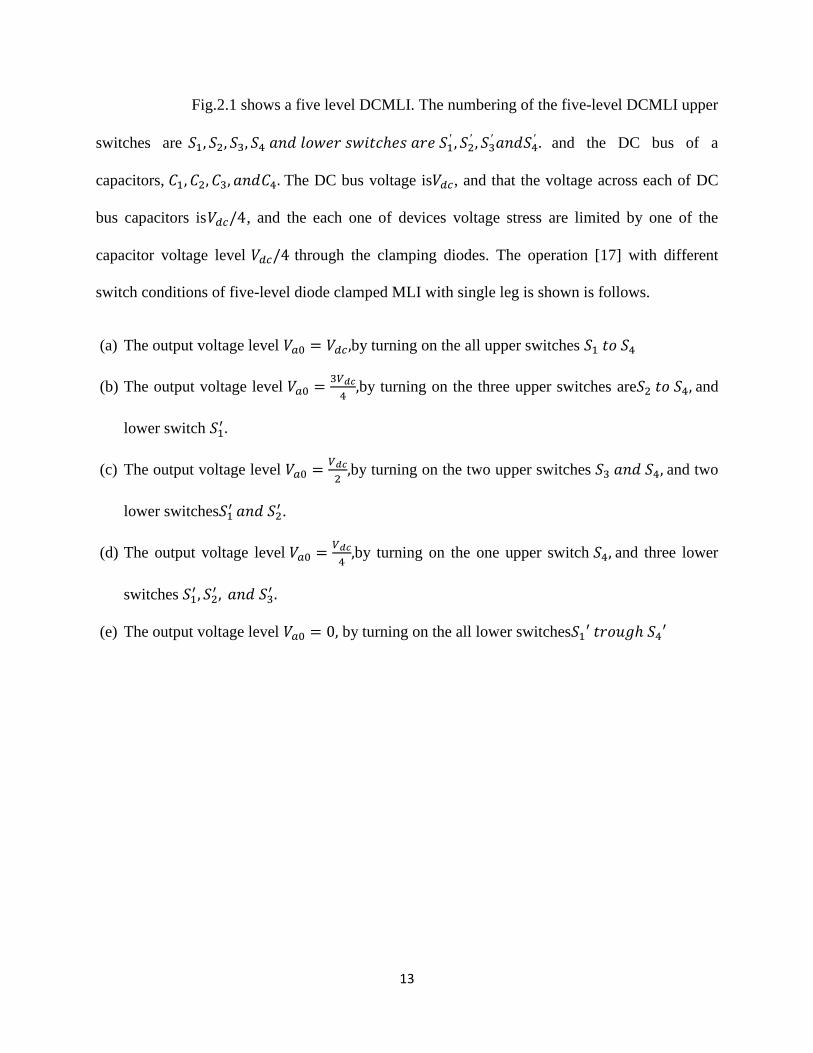
Fig.2.1 shows a five level DCMLI. The numbering of the five-level DCMLI upper
switches are 𝑆1, 𝑆2, 𝑆3, 𝑆4 𝑎𝑛𝑑 𝑙𝑜𝑤𝑒𝑟 𝑠𝑤𝑖𝑡𝑐ℎ𝑒𝑠 𝑎𝑟𝑒 𝑆1′ , 𝑆2
′ , 𝑆3′ 𝑎𝑛𝑑𝑆4
′ . and the DC bus of a
capacitors, 𝐶1, 𝐶2, 𝐶3, 𝑎𝑛𝑑𝐶4. The DC bus voltage is𝑉𝑑𝑐, and that the voltage across each of DC
bus capacitors is𝑉𝑑𝑐/4, and the each one of devices voltage stress are limited by one of the
capacitor voltage level 𝑉𝑑𝑐/4 through the clamping diodes. The operation [17] with different
switch conditions of five-level diode clamped MLI with single leg is shown is follows.
(a) The output voltage level 𝑉𝑎0 = 𝑉𝑑𝑐,by turning on the all upper switches 𝑆1 𝑡𝑜 𝑆4
(b) The output voltage level 𝑉𝑎0 =3𝑉𝑑𝑐
4,by turning on the three upper switches are𝑆2 𝑡𝑜 𝑆4, and
lower switch 𝑆1′ .
(c) The output voltage level 𝑉𝑎0 =𝑉𝑑𝑐
2,by turning on the two upper switches 𝑆3 𝑎𝑛𝑑 𝑆4, and two
lower switches𝑆1 ′ 𝑎𝑛𝑑 𝑆2
′ .
(d) The output voltage level 𝑉𝑎0 =𝑉𝑑𝑐
4,by turning on the one upper switch 𝑆4, and three lower
switches 𝑆1′ , 𝑆2
′ , 𝑎𝑛𝑑 𝑆3′ .
(e) The output voltage level 𝑉𝑎0 = 0, by turning on the all lower switches𝑆1′ 𝑡𝑟𝑜𝑢𝑔ℎ 𝑆4′

14
There are five switch combinations to obtain the output voltage as shown in the Table 2.2
Output
𝑉𝑎0
Switching condition
𝑆1 𝑆2 𝑆3 𝑆4 𝑆1 ′ 𝑆2
′ 𝑆3′ 𝑆4′
𝑉𝑎0 = 𝑉𝑑𝑐 1 1 1 1 0 0 0 0
𝑉𝑎0 =3𝑉𝑑𝑐
4
0 1 1 1 1 0 0 0
𝑉𝑎0 =𝑉𝑑𝑐
2
0 0 1 1 1 1 0 0
𝑉𝑎0 =𝑉𝑑𝑐
4
0 0 0 1 1 1 1 0
𝑉𝑎0 = 0 0 0 0 0 1 1 1 1
Table 2.2 Switching combination for a five level diode clamped inverter
2.1.2 Features of Diode-Clamped MLI
(a) Large voltage rating of blocking diodes: Each one of the switching device is required to block
a voltage level of𝑉𝑑𝑐
𝑚−1, and the clamping diodes are required to have different reverse blocking
voltage ratings. For example, when all lower four switches are turned on, one of the diode 𝐷1′
blocks the three capacitor or three times capacitor voltages, or 3𝑉𝑑𝑐/4. Diodes 𝐷2 𝑎𝑛𝑑 𝐷2′
need to block two capacitor voltages, or 𝑉𝑑𝑐/2, and 𝐷3 needs to blocks one capacitor voltage,
or𝑉𝑑𝑐/4. Even though each one of main switch is supposed to block the normal locking
voltage, the locking voltage of each of the clamping diodes are in the diode clamping multi-
level converter is depends on the position in the structure of topology.
15
(b) Unequal switching device rating: We can notice from table 1.3 that switch 𝑆1 not conduct over
the entire cycle except during the interval when𝑉𝑎𝑜 = 𝑉𝑑𝑐. And 𝑆4 not conduct only 𝑉𝑎𝑜 = 0.
so, such kind of an unequal switch conduction duty requires only when different ratings of
current for the switching devices. Therefore, if the DC-AC converter design uses for the
average duty cycle to find switching device ratings, when the upper of the switches may be
oversized, lower switches may be undersized.
(c) Unbalancing of the capacitor voltage: Because of the voltage levels at the different for
capacitor terminals, and the currents supplied by the capacitors can also be different. When
converter operating at unity power factor, and the charging time for rectifier (AC-DC) or
discharging time for inverter (DC-AC) operation for each of its capacitor is different. Such a
capacitor charging time repeats for every half-cycle, and the result it capacitor voltage is not
balanced between different levels. The unbalanced voltage problem in a multi-level inverter
can be resolved by using different approach such as capacitor can be replaced by a controlling
the constant dc voltage source these are PWM regulator, or batteries.
2.1.3 Advantages of DCMLI
The control method is simple.
The reactive power flow can be easily controlled.
If increasing the number of levels, accordinigly harmonic content is very small to avoid the
need of afilter.
The inverter can operated at higher efficiency because all of the devices are switched at a
normal or line frequency.

16
2.1.4 Disadvantages of DCMLI
If increasing the number of levels, accordingly clamping diodes are increases.
It is very difficult to control the real power flow.
2.2 Capacitor Clamped Multilevel Inverter
The flying capacitor MLI was proposed [8] by Foch and Meynard. The structure is
same as that of diode clamped multilevel inverter (DCMLI) except that clamping diodes. In this
involves series connection of clamping capacitors.
2.2.1 Operation of FCMLI
Fig.2.2 shows a three level capacitor clamped inverter. Here instead of diodes,
capacitors are used to clamp the device voltage to one of capacitor voltage level. The voltage across
𝑉𝑎𝑛 has three level of voltages are 𝑉𝑑𝑐 2⁄ , 0 and -𝑉𝑑𝑐 2⁄ by the switching combination as shown in
Table 2.3.The switching state 1 denotes that switch is ON and state 0 denotes that switch is OFF.

17
(a) (b)
Fig.2.2 Single Phase Capacitor Clamping Multilevel Converter (a) three level (b) five level
Voltage 𝑉𝑎𝑛 𝑆1 𝑆2 𝑆′1 𝑆′2
𝑉𝑑𝑐 2⁄ 1 1 0 0
0 0 0 1 1
-𝑉𝑑𝑐 2⁄ 1 0 1 0
0 1 0 1
Table 2.3 Switching combination for a three level flying capacitor clamped inverter
2
V dc
2
V dc
4
V dc
4
V dc
4
V dc
4
V dc

18
Fig 2.2 shows the one leg five-level inverter. The DC rail 0 is the reference point of the
phase voltage output. The steps to operate the five-level voltages are followed.
(a) The output voltagelevel𝑉𝑎𝑜 = Vdc by turns all upper switches.
(b) The output voltagelevel𝑉𝑎𝑜 =3Vdc
4, there are four combinations.
(i) 𝑉𝑎𝑜 = 𝑉𝑑𝑐 −Vdc
4 By turn on𝑆1, 𝑆2, 𝑆3 𝑎𝑛𝑑 𝑆4
′ .
(ii) 𝑉𝑎𝑜 =3Vdc
4 by turn on 𝑆2, 𝑆3, 𝑆4 𝑎𝑛𝑑 𝑆1
′ .
(iii) 𝑉𝑎𝑜 = 𝑉𝑑𝑐 −3Vdc
4+
Vdc
2 By turn on𝑆1, 𝑆3, 𝑆4 𝑎𝑛𝑑 𝑆2
′ .
(iv) 𝑉𝑎𝑜 = 𝑉𝑑𝑐 −Vdc
2+
Vdc
4 by turn on 𝑆1, 𝑆2, 𝑆4 𝑎𝑛𝑑 𝑆3
′ .
(c) For an output voltage level𝑉𝑎𝑜 =Vdc
2, there are six combinations.
(i)𝑉𝑎𝑜 = 𝑉𝑑𝑐 −Vdc
2 By turn on𝑆1, 𝑆2, 𝑆′3 𝑎𝑛𝑑 𝑆4
′ .
(ii) 𝑉𝑎𝑜 =Vdc
2 By turn on𝑆3, 𝑆4, 𝑆1
′ , 𝑎𝑛𝑑 𝑆2′ .
(iii) 𝑉𝑎𝑜 = 𝑉𝑑𝑐 −3Vdc
4+
Vdc
2−
Vdc
4 By turn on 𝑆1, 𝑆3, 𝑆2
′ , 𝑎𝑛𝑑 𝑆4′ .
(iv)𝑉𝑎𝑜 = 𝑉𝑑𝑐 −3Vdc
4+
Vdc
4 by turn on 𝑆1, 𝑆4, 𝑆2
′ , 𝑎𝑛𝑑 𝑆4′ .
(v) 𝑉𝑎𝑜 =3Vdc
4−
Vdc
2+
Vdc
4 by turn on 𝑆2, 𝑆4, 𝑆1
′ , 𝑎𝑛𝑑 𝑆3′ .
(vi) 𝑉𝑎𝑜 =3Vdc
4−
Vdc
4 by turn on 𝑆2, 𝑆3, 𝑆1
′ , 𝑎𝑛𝑑 𝑆4′ .
(d) For an output voltage level 𝑉𝑎𝑜 =Vdc
4, there are four combinations
(i) 𝑉𝑎𝑜 = 𝑉𝑑𝑐 −3Vdc
4 by turn on 𝑆1, 𝑆2
′ , 𝑆3′ 𝑎𝑛𝑑 𝑆4
′ .

19
(ii) 𝑉𝑎𝑜 =Vdc
4 by turn on 𝑆4, 𝑆2
′ , 𝑆3′ 𝑎𝑛𝑑 𝑆1
′ .
(iii) 𝑉𝑎𝑜 =𝑉𝑑𝑐
2−
3Vdc
4 by turn on 𝑆3, 𝑆1
′ , 𝑆2′ 𝑎𝑛𝑑 𝑆4
′ .
(iv) 𝑉𝑎𝑜 =3Vdc
4−
Vdc
2by turn on 𝑆2, 𝑆1
′ , 𝑆3′ 𝑎𝑛𝑑 𝑆4
′ .
(e) The output voltage level 𝑉𝑎𝑜 = 0 turn on all lower switches.
There are many possible switch combinations to generate output voltage is shown in the table 2.4.
Output
𝑉𝑎0
Switching condition
𝑆1 𝑆2 𝑆3 𝑆4 𝑆1 ′ 𝑆2
′ 𝑆3′ 𝑆4′
𝑉𝑎0 = 𝑉𝑑𝑐 1 1 1 1 0 0 0 0
𝑉𝑎0 =3𝑉𝑑𝑐
4
0 1 1 1 1 0 0 0
𝑉𝑎0 =𝑉𝑑𝑐
2
0 0 1 1 1 1 0 0
𝑉𝑎0 =𝑉𝑑𝑐
4
0 0 0 1 1 1 1 0
𝑉𝑎0 = 0 0 0 0 0 1 1 1 1
Table 2.4 Switching combination for a five level capacitor clamped inverter
2.2.2 Features of FCMLI
(a) A more number of capacitors: The FCMLI requires a more number of storing capacitors.
Assuming that the ratings of each capacitors is same as that of a switching device, an m-
level FCMLI requires [m-1]*[m-2]/2 balancing capacitors per one phase and also [m-1]

20
main DC bus capacitors. On the comparison of an, m-level diode-clamped MLI requires
[m-1] capacitors of the same ratings.
(b) Balancing capacitor voltages: Unlike the DCMLI, the FCMLI has reduces at its inner
voltage levels. And the voltage level is reduced, if the two or more number of valid switch
combination can be synthesize it. The availability of voltage redundancies allows
controlling the individual capacitor voltages. In order to produce the same amount of output
voltage, the FCMLI or converter can involve different capacitor combinations allowing
preferable charging or discharging of each capacitors. In order to make the flexibility easier
to manage the capacitor voltages and put them at a proper correct values. Thus the proper
selection of switching combinations, the clamping or flying-capacitor multilevel inverter
(FCMLI) may be used for the real power conversions. Howsoever, when it is involves real
power flow conversion, for selecting the switch combinations are become very
complicated, and then the switching frequency became higher than that of fundamental or
normal frequency.
2.2.3 Advantages of FCMLI
Large amounts of storing capacitors provide capability during power outages.
Real power and reactive power flow can be controlled easily.
THD is lowered with the increase in the level as in NPC.
With the more levels, the harmonic content is less and to avoid the requirement for filters.
The inverters can provide different switch combination reducing for balancing the
different voltage levels.

21
2.2.3 Disadvantages of FCMLI
Large amount of storage capacitors are required for increasing the number of levels.
The converter control can be very complicated accordingly the switching losses are very
high.
2.3 Cascaded H-bridge Multilevel Inverter
In the cascaded multilevel converter can be utilized in wide range of applications
[7, 8]. It is superior for medium and high power applications, likely FACTS controllers.
A cascaded multilevel converter (CMLI) consists of a cascaded connected of series
of H-bridge or single-phase full bridge inverter. And the function of the MLI is to sumarize a
desired voltage and several separated DC sources (SDCSs), which can be obtained from DC
batteries or solar cells. From bellow fig shows that the basic structure of cascaded inverter with
require separate DC source (SDCS). Each H-Bridge inverter connected to the separate DC source.
The terminal voltages of all H-Bridge inverters are connected in series. In CHMLI, not require for
clamping diodes and voltage-balancing capacitors. Three, five and seven level cascaded multi-
level converters are shown in fig 2.3.

22
(a) (b)
(c)
Fig.2.3 Cascaded multilevel inverter (a) three, (b) five, (c) seven level

23
2.3.1 Operation of CHBMLI
From fig 2.3 shows that the phase voltage waveform of cascaded multi-level
converter with five-level and require four separate DCSSs. The output phase voltages are analysed
by the addition of four converter outputs. The phase voltage is𝑉𝑎𝑛 = 𝑉𝑎1 + 𝑉𝑎2 + 𝑉𝑎3 + 𝑉𝑎4. And
each of converter level can generate the only three outputs are, +𝑉𝑑𝑐, 0 𝑎𝑛𝑑 − 𝑉𝑑𝑐. The DC source
is converted to AC output side by different switch combinations of the four switches. These
switches are 𝑆1, 𝑆2, 𝑆3 𝑎𝑛𝑑 𝑆4. For example, by turning on the switches 𝑆1 𝑎𝑛𝑑𝑆4 voltage 𝑉𝑎4 =
𝑉𝑑𝑐. by turning on switches𝑆2 𝑎𝑛𝑑𝑆3, 𝑉𝑎4 = −𝑉𝑑𝑐. By turning off all the switches voltage is𝑉𝑎4 =
0. And similarly, the AC side output voltage at each level can be solving in the same manner. If
number of DC sources are n, the output phase voltage levels is m= n+1. And the same manner the
number of the output line voltage level can be found by 𝑚 = (2𝐻 + 1) here, H is the number of
H-bridges in each phase.
Fig.2.4 output phase voltage of cascaded MLI

24
2.3.2 Features of CHMLI
(a) For the real power conversion from converter (AC to DC) and then inverter (DC to AC),
the cascaded multi-level converter requires separate Dc sources. The basic cascaded
inverter consist separate DC sources is suitable for various non conventional energy
sources such as fuel cells and photovoltaic cells.
(b) By connecting the DC source in between the two converter in a can cantination (back-to-
back) manner is not possible. Because there is a short circuit can be introduced when these
back-to-back converters are not properly switching simultaneously.
2.3.3 Advantages of CHMLI
Compared with DCMLI, FCMLI, it requires less number of devices to achieve same
number of output voltage levels.
In order to reduce the switching losses and switching stresses Soft-switching techniques
can be used.
Optimized circuit layout and packaging are possible.
No clamping diodes are present as in NPC.
No EMI problem.
Less common mode voltage and less𝑑𝑣 𝑑𝑡⁄ .
It can work at reduced power level when one of its cells is damaged.
The number of output voltage levels is double the number of DC sources(𝑚 = 2𝑠 + 1).

25
2.3.4 Disadvantages of CHMLI
It requires for separate DC sources of each bridge for real power conversions, so its
applications are very limited.
2.4 Applications of MLI
Multilevel converter are better suitable for medium and large power applications such
as in effect of systems for controlling the sources of reactive power. In the drunken state operation,
a converter can produce a controlled reactive current. And it can be operated as a static volt-ampere
reactive (VAR) compensator (STATCON) [17]. Also, these MLI can be reduces the size and
weight of the compensator. And also improves the performance of the compensator during power
system contingencies. The use of a large voltage DC-AC converter makes a possible direct
connection to the large voltage distribution system, and to eliminating the low secondary voltage
transformer and to reducing cost of the system. In addition, the harmonic ripples content of the
inverter waveform can also be reduced with convenient modulation control techniques and thus
the system efficiency can be improved. Some of the applications of MLI include (1) reactive power
compensation, (2) back to back intertie, and (3) variable speed drives.
2.5 Summary of MLI
The multilevel converter can be applied to motor speed drives applications. These
MLI offer a less output voltage harmonic distortion (THD), higher efficiency and also the power
factor also near unity.

26
The main advantages of MLI including the following,
They can be suitable for medium and large-voltage and large-current applications.
They have operated at efficiency levels very high because each of devices are switched at
a less frequency.
The power factor is very high and it is nearer to unity for MLI are used for rectifiers to
convert AC level to DC level.
There is no EMI problem.
There is no charge unbalance result when the inverters are in the either rectifier mode or
inverter mode (drive mode).

27
Chapter-3
MODULATION TECHNIQUES
Modulation introduction
Modulation techniques
Multi-carrier PWM

28
MODULATION TECHNIQES
3.1 Modulation Introduction
In the power electronics converters are mainly operated in the switched-mode. That
means these switches are always operated either in one of these two states turned on-only small on
state voltage drop across the switch, turned off -state no current flows. The operation from
conducting state to non- conducting state, occurring a losses and power dissipation of switches
rises. In order to controlling the power flow in the inverter, the switches can be operated between
the on and off states. This can be happens only when the capacitors and inductors at the input side
and output side filter the switching signal. To attenuate the switching components and the desired
less frequency AC components or DC retained. This kind of process can be called as pulse-width
modulation (PWM), and the DC value can be controlled by changing the period of the pulses. For
higher attenuation or tuning of the switching components, the carrier frequency or switching
frequency should very high compared to the fundamental AC frequency or reference frequency
seen at the both input or output terminals. In the large power electronics converter, this is in combat
with an upper-limit placed on carrier frequency by its switching losses. If the ratio of carrier
frequency to the reference frequency may be very less for GTO converters. In one more application
where the number of pulses low in converters which are described better for amplifiers. In the high
power switched-mode amplifiers applications are active power filtering, signal generation and etc.
3.2 Modulation Techniques
In this chapter describes various modulation techniques to control the output voltage
of the multilevel voltage source inverter [18]. Broadly, these control techniques can be classified
into Pulse-Width Modulation (PWM), Selective Harmonic Elimination (SHE) and one more is

29
Optimized Harmonic Stepped Waveform (OHSM) [1]. The PWM techniques preferable for open
loop type like sinusoidal PWM, Space Vector Modulation, sigma-delta and closed loop type like
hysteresis current controller, linear current controller etc.
PWM can be considered to be an efficient modulation technique as it does not require
additional components and also the lower harmonics can be eliminated or minimized leaving
higher order harmonics which can be easily filtered out whereas the requirement of SCRs in this
technique with less turn-on tme and less turn-off times makes it expensive.
Sinusoidal PWM (SPWM) is the simplest method that can be implemented in both
two level and higher level inverters. Basically, in SPWM, there are two signals - reference signal
and a large frequency triangular signal (carrier signal) are compared to give two states (high or
low). The magnitude of the fundamental or reference component of the output current or voltage
of the inverter can be controlled by changing Modulation Index (𝑀𝐼). The Modulation Index can
be defined as the ratio of the magnitude of the reference voltage signal (𝑉𝑟) to that of the magnitude
of the carrier voltage signal (𝑉𝑐). Thus, by keeping𝑉𝑐 constant and varying𝑉𝑟, the modulation index
can be varied.
3.3 SPWM of a Single Phase Inverter
There are two types of SPWM techniques (a) unipolar pulse width modulation (b) bi-
polar pulse width modulation [17] which are used in a single phase cascaded bridge inverter to
vary its output voltage.

30
3.3.1 Bipolar Pulse Width Modulation
In this modulation method, the gate pulses are obtained by comparing a low
frequency sinusoidal modulating signal and reference signal with a large-frequency triangular
carrier signal. The wave form of bipolar PWM method is shown in fig. It compare with triangular
wave and sinusoidal waveforms and generated pulses and it gives to the switching device and
produce line voltage shown fig 3.1.
Fig .3.1 Bipolar Pulse Width Modulation
Fig 3.2 line voltage waveform for bipolar modulation
0 0.005 0.01 0.015 0.02 0.025 0.03 0.035 0.04 0.045 0.05-3
-2
-1
0
1
2
3
Time (secs)
Am
plit
ude
0 0.005 0.01 0.015 0.02 0.025 0.03 0.035 0.04 0.045 0.05
-200
-150
-100
-50
0
50
100
150
200
Time (sec)
LINE
VOL
TAGE
(V)

31
3.3.2 Unipolar Pulse Width Modulation
This modulation method needs two sinusoidal waveforms. And these are of same
amplitude and frequency require 180 degree out of phase. The DC-AC converter output voltage
either between the zero and +𝑉𝑑during the first half-cycle and between zero and –𝑉𝑑 during the
second half-cycle during the frequency should be fundamental. This modulation is also possible
with two triangular carrier waves and one sinusoidal modulating signal. The line voltage waveform
and unipolar PWM shown in fig.3.3 and fig.3.4.
Fig.3.3 Unipolar Pulse Width Modulation
Fig.3.4 Output voltage waveform for unipolar modulation
0 0.005 0.01 0.015 0.02 0.025 0.03 0.035 0.04 0.045 0.05-6
-4
-2
0
2
4
6
Time (secs)
Ampl
itude
0.01 0.02 0.03 0.04 0.05 0.06 0.07 0.08 0.09 0.1-400
-300
-200
-100
0
100
200
300
400
Time (secs)
Line v
oltag
e Vab
(volts
)

32
3.4 Multicarrier Pulse Width Modulation Techniques
The multiple-carrier based PWM method for cascaded converters are broadly
classified into two types (i) phase shifting modulation (ii) level shifting modulation. In both the
motheds, for an m level converter require [m-1] triangular carrier waves. And all of the triangular
(carrier) waves should have same frequency and also the peak-peak magnitude should be same.
3.4.1 Level Shifting Multiple-carrier Modulation Technique
In Level Shifting PWM (LSPWM), the triangular waves are displaced vertically. So
the bands occupy contiguously. The modulation of the frequency is given by 𝑚𝑓 = 𝑓𝑐𝑟
𝑓𝑚 and
amplitude modulation index is𝑚𝑎 =𝑉𝑚𝐴
(𝑚−1)𝑉𝑐𝑟, where 𝑓𝑚and 𝑓𝑐𝑟are the frequencies of the reference
(modulating) and triangular (carrier) waves and 𝑉𝑚𝐴and 𝑉𝑐𝑟 are the peak amplitudes of reference
(modulating) and triangular (carrier) waves respectively. The magnitude of modulation lies in the
range of 0 to 1. Depending upon the disposition of the carrier waves, level shifted PWM can be
(i) In Phase Disposition pulse width modulation method (IPD – PWM)
(ii) Phase Opposition Disposition pulse width modulation method (POD – PWM)
(iii) Alternate Phase Opposition Disposition pulse width modulation method (APOD –
PWM).
IPD PWM
This modulation method, all the triangular (carrier) waves are in phase as shown in
Fig.3.5. In m level multi-level converter require (m-1) triangular waves and large frequency
triangular wave is compare with fundamental sinusoidal wave and generate pulses.

33
Fig.3.5 In Phase Disposition PWM for five level multilevel inverter
POD PWM
The triangular waveforms are in all the phase of above zero reference are in phase
and below the zero reference value are inphase; but there is a 180° phase difference between the
ones upper and lower zero respectively as shown in the Fig.3.6. in this positive group and nagative
group are phase shifted by 180 degrees.
Fig.3.6 Phase opposition Disposition PWM for five level multilevel inverter
0 0.002 0.004 0.006 0.008 0.01 0.012 0.014 0.016 0.018 0.02-2
-1.5
-1
-0.5
0
0.5
1
1.5
2
Time (secs)
Am
plitu
de
0 0.002 0.004 0.006 0.008 0.01 0.012 0.014 0.016 0.018 0.02-2
-1.5
-1
-0.5
0
0.5
1
1.5
2
Time (secs)
Am
plitu
de

34
APOD PWM
The carrier waves have to be displaced from each other by 180° phase difference
alternately as shown in Fig.3.7. In this triangular wave are alternatly phase difference by 180°.
Fig.3.7 Alternate Phase opposition Disposition PWM for five level multilevel inverter
3.5 Summary
Multilevel inverters can achieve an effective increase in overall switch
frequency through the cancellation of the low order switch frequency terms. This unit has
explained different types of carrier based PWM modulation techniques. PWM techniques are
advantageous in controlling the output voltage and minimizing the harmonics. There are many
modulation methods for multilevel inverters. But carrier based modulation method is easy and
efficient. The PWM output spectra were calculated from basic operation explained above
in phase disposition method and simulated using MATLAB (SIMULINK).
0 0.002 0.004 0.006 0.008 0.01 0.012 0.014 0.016 0.018 0.02-2
-1.5
-1
-0.5
0
0.5
1
1.5
2
Time (secs)
\Am
plit
ud
e
35
Chapter-4
THE PROPOSED TOPOLOGY
Introduction on proposed topology
Three-phase un-control diode rectifier
Single DC source fed cascaded converter
AC LCL resonant converter along with transformer

36
THE PROPOSED TOPOLOGY
The proposed topology consisting of three-phase diode rectifier, multi-level inverter,
the AC L-C-L resonant converter and output stage shown in fig.4.1.
Fig.4.1 Simplified diagram of proposed topology
In the proposed topology consist of
The input of the supply is given to the three-phase un-controlled full wave diode bridge
rectifier. From the output side of rectifier or dc bus side, a large capacitor is connected
to reduce the ripple content in voltage. The drawback of such kind of rectifier is very
high harmonic component in the line current side. So, which is lead to very less power
factor. To place an inductor in to the dc bus, to minimize the THD of line current and
also the power factor can be improved.

37
A diode clamped multi-level inverter and single DC source fed cascaded MLI is
utilized, and to avoid switching losses and PWM switching at each level is not
implemented and a staircase output is employed.
The output of MLI, the AC L-C-L resonant converter is connected along with the
transformers that provide isolation at the output side. For each of the transformers a
1:1+1 turn’s ratio can be employed. And it gives an overall turn’s ratio of 8:1. So the
coupling of the transformer can be improved. So that the leakage reactance was
minimized.
Synchronous rectifiers are fitted to secondary of transformers connecting in parallel.
Smoothing of the ripple in the voltage can be applied to the load is reduced using a DC
L-C-L filter.
4.1 Three-Phase Un-Controlled Diode Rectifier
The input section consist 3-phase un-controlled diode bridge rectifier. A three-phase
AC supply is given to the diode rectifier and it is converted to DC average voltage. In the full-
wave diode rectifier consists of six diodes shown in fig.4.2. Upper diodes are 𝐷1, 𝐷3, 𝐷5 constitute
the positive side of diodes and lower diodes 𝐷2, 𝐷4, 𝐷6 from the negative side of diodes. If three-
phase supply 400 V and 50 Hz supply is given the three-phase bridge rectifier and produce output
DC average voltage 540 V.
38
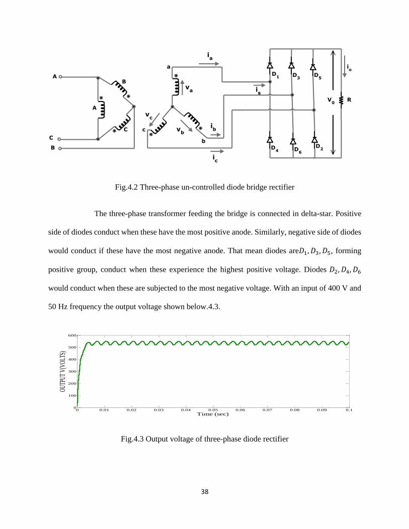
Fig.4.2 Three-phase un-controlled diode bridge rectifier
The three-phase transformer feeding the bridge is connected in delta-star. Positive
side of diodes conduct when these have the most positive anode. Similarly, negative side of diodes
would conduct if these have the most negative anode. That mean diodes are𝐷1, 𝐷3, 𝐷5, forming
positive group, conduct when these experience the highest positive voltage. Diodes 𝐷2, 𝐷4, 𝐷6
would conduct when these are subjected to the most negative voltage. With an input of 400 V and
50 Hz frequency the output voltage shown below.4.3.
Fig.4.3 Output voltage of three-phase diode rectifier
0 0.01 0.02 0.03 0.04 0.05 0.06 0.07 0.08 0.09 0.10
100
200
300
400
500
600
Time (sec)
OUTP
UT V
(VOL
TS)
39
From the output side of rectifier or dc bus side, a large capacitor is connected to
reduce the ripple content in voltage. The drawback of such kind of rectifier is very high harmonic
component in the line current side. So, which is lead to very less power factor. To place an inductor
in to the dc bus, to minimize the THD of line current and also the power factor can be improved.
The DC is given to the multi-level converter and it produce the stair case output voltage waveform.
In the previous chapter explained different types of multi-level inverter along with merits and
demerits. The, MLI output stair case voltage waveform is given to the AC L-C-L resonant
converter along with planar transformer.
4.2 Single DC Source fed Cascaded Multilevel Inverter
In the previous chapter explored the importance of cascaded multilevel inverter.
Further, pulse width modulation techniques are also introduced. But it is concluded that CHML
has a greatest limitation, is that every H-Bridge cell require separate DC source [1]. In this we
investigated cascaded multilevel converter with one DC source using transformers. With this we
try to minimize the total number of DC sources and thereby cost and complexity of converter.
4.2.1 Cascade H-bridge Multilevel Converter by employing separate DC sources
In the previous chapter explored that CHMLI with employing separate DC source.
But, it is concluded that CMLI has a great limitation is that every H-Bridge cell require separate
DC source. In m-level cascaded H-Bridge converter shown below, and it require separate DC
source for each H-Bridge that mean m-level cascaded converter consist of 𝑚−1
2 DC sources [8].
Each full-bridge DC-AC converter produce three output levels and all the H-Bridges are connected
in series. So, the output voltage can be added to the all the H-Bridge and gives stair case waveform.

40
If the total number of levels are increases, the output voltage waveform is more stair
case wave and it looks like a sinusoidal. In multilevel converter has so many advantages, if increase
levels the total harmonic distortion can be minimize and reduce𝑑𝑣
𝑑𝑡. Each H-Bridge consist a full-
bridge inverter and require separate DC source. This is the greatest limitation in the cascaded
multilevel converter and if increase levels accordingly Dc sources also increases. So, in order to
reduce number of DC sources employing new topology. In this only one DC source require and
employing single-phase transformers. By connecting transformers the output waveform will be
very smoother due to transformer leakage reactance and also complexity reduces.
Fig.4.4 m-level cascaded h-bridge multi-level converter

41
4.2.2 Cascaded H-bridge Multilevel Converter with single DC source by employing single-
phase transformer
Fig.4.5. shows the cascaded multilevel converter (CHBMLI) with only one DC
source by employing the single-phase isolation transformers. By employing single-phase
transformers with every H-Bridge this can be easily connected to the grid [1]. In CHMLI, each
bridge generates a three output levels voltage of +𝑉𝑑𝑐, 𝑧𝑒𝑟𝑜 𝑎𝑛𝑑 − 𝑉𝑑𝑐. similarly, the rest of the
bridges also generates the same voltage levels. But, at the end of all voltage levels are added up
with single-phase transformers. So, the shape of the output voltage levels is like a stepped
waveform. The operation is same as conventional cascaded multilevel inverter but voltages are
added up through single-phase transformers.
Fig.4.5 Cascaded five level multilevel inverter with single DC source
Fig shows the five-level output is observed in the output waveform. The waveform
is smoother due to the presence of leakage reactance of the transformers. Further, isolation can
also provide and need to avoid output filter because of transformers. It is know that due to

42
transformer leakage reactance easily nullify higher order harmonicas. One of the H-Bridge
operated in PWM mode and remaining are fundamental switching mode only. This can be helpful
for reducing switching losses and efficiency increases.
Advantages:
(i) Complexity can be drastically reduced.
(ii) Improving reliability.
(iii) The price of converter comes down because of require one DC source.
(iv) The output waveform is smoother due to transformer leakage reactance..
Disadvantages:
(i) Usage of many transformers. For an every additional level transformers count
increases.
4.3. AC L-C-L Resonant Converter along with transformer
4.3.1 AC L-C-L Resonant Converter
The features of resonant converters are zero current switching (ZCS), zero voltage
switching (ZVS), and efficiency is high, size will be small and there are no EMI problems.
Resonant converters are successfully applied to AC power supplies for improving the power factor
and heating, DC power supplies for domestic and industrial applications [10, 11 and 12]. There
are two types of basic resonant converters series and parallel RC. The series RC has better part-
load efficiency and lack of DC blocking voltage of the transformer due to the series connected
capacitor in RC. But, its load regulation is poor and output voltage regulation is not possible in the

43
no-load condition. But, the PRC offers good no-load regulation and load efficiency is poor and
lack of DC blocking of the transformer.
Fig.4.6 AC LCL resonant converter and transformer
Fig.4.6. shows that the AC L-C-L resonant network formed with the components
𝐿1, 𝐶1 𝑎𝑛𝑑 𝐿2, along with the planar transformer connected at output stage and it provide isolation.
The values of inductances and capacitance are chosen for the AC L-C-L resonant network are
resonance at the output frequency of MLI. From the fig, at node
𝑉𝑥 = 𝑉1 + 𝑉2
From above equation voltage across𝐿1 will be 𝑉2 and the voltage across 𝐿2 will
be𝑉1. The output current of AC L-C-L resonant network, 𝐼2, can be controlled by controlling the
multilevel-inverter output voltage 𝑉1.For, electroplating process require the power supply low
voltage DC and high current DC, but multilevel inverter output voltage is very high. So by using

44
L-C-L resonant converter the output voltage can be reduces. Furthermore, the multilevel inverter
output voltage 𝑉1 is more compare to L-C-L network output voltage 𝑉2. But the, merit of L-C-L
resonant converter is to maintain the constant current source, that means current through 𝐿1 is
equal to the current through 𝐿2i.e 𝐼1 = 𝐼2.
4.3.2 Advantages of AC L-C-L Resonant Converter
Parallel operation is very easy and less circulating currents at lightly load conditions.
For AC power supplies it can improve power factor.
The ripple in the peak-peak output current is reduced.
The ripple frequency can be increased and reducing need of filtering requirements.
The total harmonic distortion (THD) reduced.
No EMI problems.
Further, the output of AC L-C-L resonant converter connected to primary winding
of planar transformers. In order to increase the current levels the planar transformer connected in
the shown in fig above. That means there are eight transformers connected in primary side series
and secondary side parallel with center tapped for isolation purpose. Primary windings are
connecting in series the high voltage can be distributed each of primary winding with an equal
voltage distribution assured by connecting the secondary side windings in parallel. Similarly, the
parallel connection the high current to be distributed each of secondary winding with an equal
current assured by connecting the primary in series. From the above connection use planar
transformer so many advantages like coupling improve, leakage inductance reduces, stray
capacitance can be minimized, and skin effect and the losses in the secondary side can be also
reduced. In the primary winding series and each transformer is center tapped with 1:1+1 turns ratio

45
employed, which give the total number of turns ratio 8:1 shown fig above. Rectifiers are connected
secondary winding of each transformer to allow smoothing the output current ripple to achieve
using a DC L-C-L filter.
To increase the load resistance, the voltage 𝑉2 across 𝐿1 will be increase. Thus,
cause current drawn from MLI is increase. Due to the inductance 𝐿2and transformers the current
supplied from the load will decreases. Decreasing load current causes due to division of current
through transformers and higher load resistance. Therefore, a limit exist the size of the output load
that can be used with AC resonant converter and the transformers. Further, electroplating process
require load is 12 V DC and 500 A DC and20𝑚Ω. And load decrease a very low value the current
levels are increase high value. This load can be influences determine the value of𝐶1 in AC L-C-L
resonant network. The value of𝐶1, AC L-C-L resonant converter operate at resonant frequency
must high relative to reflected the load impedance. If, take the capacitance value is low it reduce
its effectiveness. The output stage of these we provide DC L-C-L filter with a components of
𝐿3, 𝐶2𝑎𝑛𝑑 𝐿4.
4.3.3 Effect of Transformer winding Capacitance
The AC L-C-L resonant converter connected to the transformer primary winding.
In which transformer has some winding capacitance, due to transformer internal winding
capacitance severe degradation in the output current regulation [13] that means there is a reduction
in the output current? The presence of transformer internal winding capacitance in the circuit, the
third order L-C-L converter changes to the fourth order LC-LC structure. The fourth order LC-LC
topology also maintain current source is constant. Thus, the transformer winding capacitance and

46
leakage reactance are effectively utilized part of AC L-C-L resonant converter, thereby improving
output characteristics.
Fig.4.7 Full-bride L-C-L RC along with transformer winding capacitance.
Fig.4.7. shows that the full-bridge AC L-C-L resonant converter along with full-
bridge rectifier. Components of the resonant converter are𝐿1, 𝐿2, 𝐶 and the full-bridge inverter
switches 𝑎𝑟𝑒 𝑆1, 𝑆2, 𝑆3 𝑎𝑛𝑑 𝑆4. The inverter drives the input to the resonant converter with large-
frequency square wave voltage 𝑉𝑖𝑛 with amplitude of±𝑉𝑑𝑐. Output of the AC L-C-L filter fed to
the diode rectifier and filter capacitance convert AC to DC. A transformer with 1:n turns ratio is
connected to the output of AC L-C-L resonant network and produces output current 𝐼0, output
voltage 𝑉0 with a input of 𝑉𝑑𝑐. The transformer has leakage inductance 𝐿𝑙 and winding capacitance
𝐶′𝑤𝑐 shown in fig above. The winding capacitance can be transferred to primary with turns ratio
of 1:n is 𝐶𝑤𝑐 = 𝑛2𝐶′𝑤𝑐.The AC L-C-L resonant converter behaves as constant current source and
transformer inductance is observed with a total inductance 𝐿𝑡 = 𝐿2 + 𝐿𝑙 and 𝐿1. The circuit can
be operated at the resonant frequency of𝜔𝑜 =1
√𝐿1𝐶.
47
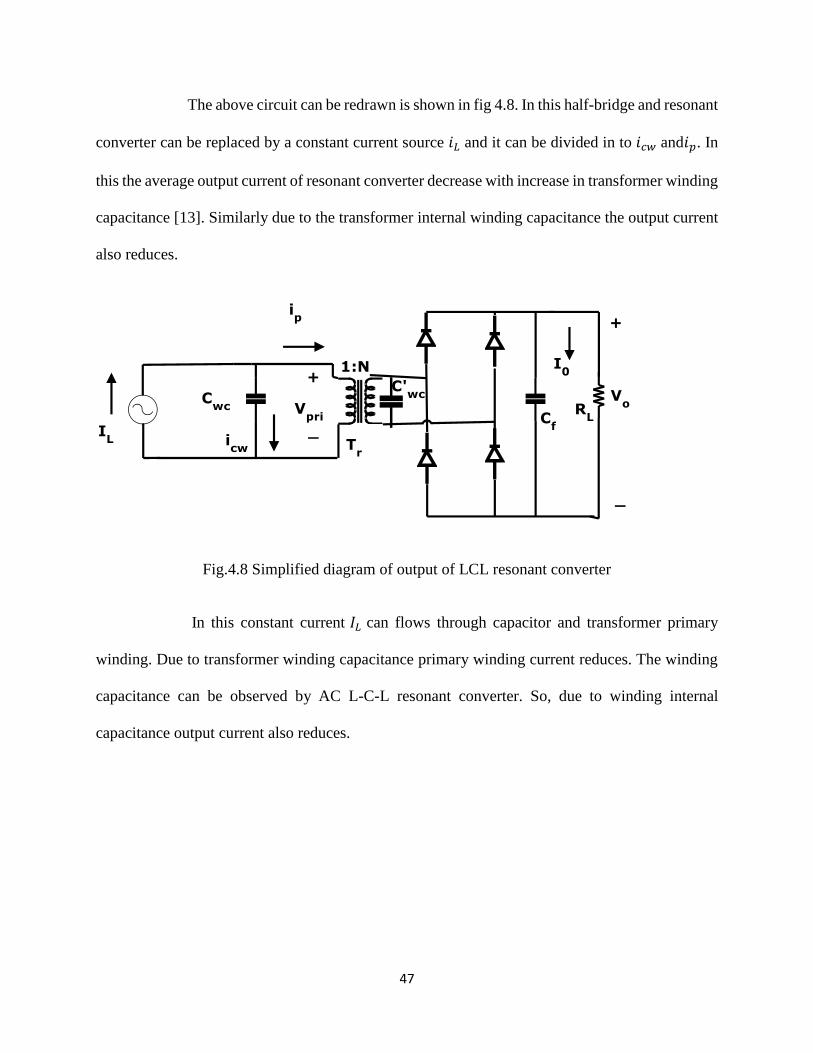
The above circuit can be redrawn is shown in fig 4.8. In this half-bridge and resonant
converter can be replaced by a constant current source 𝑖𝐿 and it can be divided in to 𝑖𝑐𝑤 and𝑖𝑝. In
this the average output current of resonant converter decrease with increase in transformer winding
capacitance [13]. Similarly due to the transformer internal winding capacitance the output current
also reduces.
Fig.4.8 Simplified diagram of output of LCL resonant converter
In this constant current 𝐼𝐿 can flows through capacitor and transformer primary
winding. Due to transformer winding capacitance primary winding current reduces. The winding
capacitance can be observed by AC L-C-L resonant converter. So, due to winding internal
capacitance output current also reduces.

48
Chapter-5
SIMULATION RESULTS
Introduction on simulation
Simulation results by five-level diode clamped converter
Simulation results on five level single DC source fed cascaded converter
FFT analysis on DCMLI and CHMLI
Conclusion on simulation results

49
SIMULATION RESULTS
In order to develop small voltage large current and the operation of proposed
applications like DC arc welding, electroplating and some industrial applications, a multi-level
converters along with AC LCL resonant converter is studied. To generate such low voltage and
large current power supplies and to drive arc welding and electroplating process. In order to
develop such kind of power supplies the MATLAB-simulation can be used to simulate the five-
level diode clamping multi-level inverter and single DC source fed cascaded multi-level convers.
5.1 Simulation Results by using five-level Diode Clamped Multi-level Converter:
Five-level converter can be simulated by using the theory explained by second
chapter. In order to simulate five-level DCMLI, the pulses are given to the switching devices. Here
use level shifted pulse width modulation like IPD technique. An five-level converter require four
high frequency triangular waveforms and low frequency sinusoidal waveform with a modulation
index of 0.8, and both waveforms are compare and generate pulses. These pulses are given to the
switching devices to produce an output. In the give bellow the proposed topology consist a five-
level two leg multi-level converter. Output of three-phase diode rectifier output is given to the
DCMLI with an input of 400 V AC and 50 Hz frequency. The multi-level inverter produce with
an output voltage 540 V stair case AC waveform is shown in bellow. The modulation index will
be 0.8 with a fundamental frequency of 50 Hz.

50
Fig.5.1 Single-phase five-level bridge diode clamped multi-level converter
Fig.5.2 Output voltage waveform of five-level DCMLI
4
V dc
4
V dc
4
V dc
4
V dc
0 0.05 0.1 0.15 0.2 0.25 0.3 0.35 0.4 0.45 0.5-600
-400
-200
0
200
400
600
Time (secs)
ML
I O
UT
PU
T V
(VO
LT
S)

51
The output voltage of multi-level convert is given to the AC L-C-L resonant
converter and it can maintain the current should be constant and also to reduce the total harmonic
distortion in the output voltage waveform. The current flowing through inductor 𝐿1is same as
current flowing through inductor𝐿2. The waveforms of current through 𝐿1𝑎𝑛𝑑 𝐿2 shown in fig
5.3.
Fig.5.3 Current flowing through inductor 𝐿1
Fig.5.4 Current flowing through inductor 𝐿2
0.05 0.1 0.15 0.2 0.25 0.3 0.35 0.4-40
-20
0
20
40
Time (secs)
I1(A
MP
S)
0.05 0.1 0.15 0.2 0.25 0.3 0.35 0.4-40
-20
0
20
40
Time (secs)
I2(A
MP
S)

52
The output of the resonant converter along with planar transformer with a turns
ratio of 8:1 and each transformer with center tapped full-wave rectifier and produce DC large
output current and low voltage for input with low current and large voltage. The output
waveforms of voltage and currents are shown in fig 5.5 and fig 5.6.
Fig.5.5 Output DC load current
Fig.5.6 Output DC voltage
0.05 0.1 0.15 0.2 0.25 0.3 0.35 0.4
0
50
100
150
200
250
Time (seconds)
OU
TP
UT
CU
RR
EN
T(A
MP
S)
0.05 0.1 0.15 0.2 0.25 0.3 0.35 0.4-1
0
1
2
3
4
5
6
Time (secs)
OU
TP
UT
VO
LT
AG
E(V
OL
TS
)
53
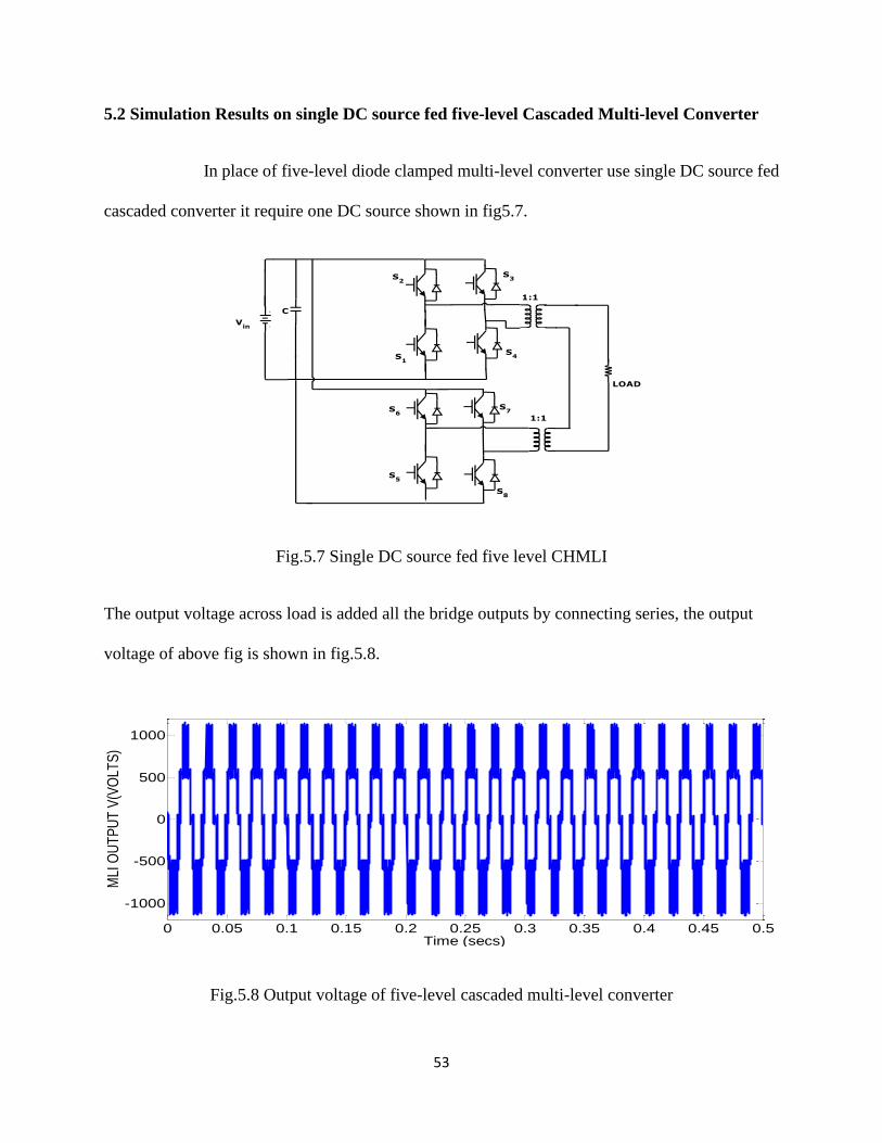
5.2 Simulation Results on single DC source fed five-level Cascaded Multi-level Converter
In place of five-level diode clamped multi-level converter use single DC source fed
cascaded converter it require one DC source shown in fig5.7.
Fig.5.7 Single DC source fed five level CHMLI
The output voltage across load is added all the bridge outputs by connecting series, the output
voltage of above fig is shown in fig.5.8.
Fig.5.8 Output voltage of five-level cascaded multi-level converter
0 0.05 0.1 0.15 0.2 0.25 0.3 0.35 0.4 0.45 0.5
-1000
-500
0
500
1000
Time (secs)
MLI
OU
TP
UT
V(V
OLT
S)
54
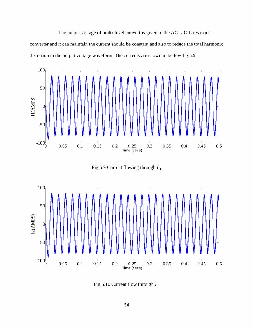
The output voltage of multi-level convert is given to the AC L-C-L resonant
converter and it can maintain the current should be constant and also to reduce the total harmonic
distortion in the output voltage waveform. The currents are shown in bellow fig.5.9.
Fig.5.9 Current flowing through 𝐿1
Fig.5.10 Current flow through 𝐿2
0 0.05 0.1 0.15 0.2 0.25 0.3 0.35 0.4 0.45 0.5-100
-50
0
50
100
Time (secs)
I1(A
MP
S)
0 0.05 0.1 0.15 0.2 0.25 0.3 0.35 0.4 0.45 0.5-100
-50
0
50
100
Time (secs)
I2(A
MP
S)

55
The DC output waveforms of voltage and currents are shown in fig.5.11. With
input AC 400 V the output DC voltage is 5 V and DC current 580 A.
Fig.5.11 Output load current
Fig.5.12 Output load DC voltage
0.05 0.1 0.15 0.2 0.25 0.3 0.35 0.4-100
0
100
200
300
400
500
600
Time (secs)
OU
TP
UT
CU
RR
EN
T(A
MP
S)
0.05 0.1 0.15 0.2 0.25 0.3 0.35 0.4-1
0
1
2
3
4
5
6
Time (secs)
OU
TP
UT
VO
LT
AG
E(V
OL
TS
)

56
5.3 FFT analysis of Diode Clamped MLI
The FFT analysis of three and five level diode clamped MLI are shown below fig.5.13.
Fig.5.13 FFT analysis of three-level DCMLI
Fig.5.14 FFT analysis five-level DCMLI
0 2 4 6 8 10 12 14 16 18 200
2
4
6
8
10
12
Harmonic order
Fundamental (50Hz) = 18.53 , THD= 60.69%
Mag
(%
of
Fu
nd
am
en
tal)
0 2 4 6 8 10 12 14 16 18 200
0.5
1
1.5
2
2.5
3
3.5
4
4.5
Harmonic order
Fundamental (50Hz) = 478.7 , THD= 32.73%
Mag
(%
of
Fu
nd
amen
tal)

57
5.3 FFT analysis of Cascaded MLI
FFT analysis of three, five, seven level cascaded MLI shown below
Fig.5.15 FFT analysis three level CHMLI
Fig.5.16 FFT analysis five level CHMLI
0 2 4 6 8 10 12 14 16 18 200
2
4
6
8
10
Harmonic order
Fundamental (50Hz) = 96.98 , THD= 55.47%
Mag
(%
of
Fund
amen
tal)
0 2 4 6 8 10 12 14 16 18 200
0.5
1
1.5
2
2.5
3
3.5
4
Harmonic order
Fundamental (50Hz) = 1016 , THD= 30.56%
Mag
(%
of
Fu
nd
amen
tal)

58
Fig.5.17 FFT analysis seven level CHBMLI
The FFT analysis of five-level CHMLI after connecting the AC L-C-L resonant converter
reduces 30.35% to 3.37% is shown fig bellow.
Fig.5.18 FFT analysis of five level CHMLI with AC L-C-L filter
By compare total harmonic distortion for DCMLI and CHMLI, the CHMLI is more advantages
than DCMLI. The THD will compare both the converters shown below table 5.1.
0 2 4 6 8 10 12 14 16 18 200
0.5
1
1.5
2
2.5
3
Harmonic order
Fundamental (50Hz) = 1550 , THD= 19.56%
Mag
(%
of
Fu
nd
amen
tal)
0 2 4 6 8 10 12 14 16 18 200
0.1
0.2
0.3
0.4
0.5
0.6
0.7
0.8
0.9
Harmonic order
Fundamental (50Hz) = 101.2 , THD= 3.37%
Mag
(%
of
Fu
nd
am
en
tal)

59
m-level multi-level converter Harmonic content (%)
Diode clamped MLI Cascaded MLI
Three-level MLI 60.67 55.47
Five-level MLI 32.73 30.56
Seven level MLI 21.5 19.56
Table 5.1 THD comparison
5.5 Conclusion on Simulation Results
By compare the simulation results with FFT analysis cascaded multi-level inverter
less harmonic distortion with increasing number of levels it can be reduced accordingly, and also
compare output voltage of MLI is double for CHMLI by compare of DCMLI. The power supplies
requires for arc welding and electroplating process 10 V DC and 550 A DC. It can be develop by
using cascaded multilevel converter with single DC source. But, diode clamped multilevel
converter develop voltage 5 V DC and current 250 A DC with input AC supply of 400 V and 50
Hz. So, cascaded multilevel converter more applicable for arc welding and electroplating process.

60
Chapter-6
CONLUSION

61
CONCLUSION
A power supply used for very large current and small voltage applications such as arc
welding, electroplating and some industrial application, has been presented here.
For large output current levels, the power supply can be developed using power MOSFETs
low voltage and small current ratings.
Isolation also provided by using a less number of turns and easily constructed Nano
crystalline transformers, and it has been shown that the power supply can acts as a current
source at short circuit and full load conditions.
62
REFERENCES
[1]. Y. Suresh, A.K Panda, “Research on Cascaded Multilevel Inverter by Employing Three-
Phase Transformers,” IET power electronics, vol. 5, pp. 561-570, 2012.
[2]. Zhong Du, Tolbert, Chiasson, “A cascade multilevel inverter using a single DC source”,
Applied Power Electronics Conference and Exposition. (APEC), 2006.
[3]. P. Yunqing, J. Guibin, L. Haitao, and W. Zhaoan, "Development of high current power
supplies for electroplating," Proc. Power Elec. Spec. Conf. (PESC), 2002, vol.1, pp. 21-23.
[4] Z. Weimin, D. Minghai, P. Yunqing, and W. Zhaoan, "Design and optimization of high
current power supply for electrochemistry," Proc. Power Elec. Conf. (IPEC), 2010, pp. 86-91
[5] S. Lejia, H. Jun, P. Yunqing, and W. Zhaoan, "Design and optimization of high current
intelligent waveform power supply for electroplating”, Proc. Power Elec. and Motion Control
Conf. (IPEMC), 2012, pp. 1516-1521
[6]. L. Jih-Sheng and P. Fang Zheng, "Multilevel converters-a new breed of power converters,"
IEEE Trans. Ind. App., 1996, vol. 32, pp. 509-517
[7]. L. M. Tolbert, F. Z. Peng, and T. G. Habetler, “Multilevel converters for large electric
drives”, IEEE Trans. Ind. Appl., 1999, vol. 35, pp. 36–44
[8]. J. Rodriguez, J.-S. Lai, and F. Z. Peng, “Multilevel inverters: A survey of topologies,
controls, and applications”, IEEE Trans. Ind. Electron., 2002, vol. 49, pp. 724–738.
[9] B. W. Carsten, "The low leakage inductance of planar transformers; fact or myth?," Proc.
Applied Power Elec. Conf. and Expo. (APEC), 2001, vol.2, no., pp.1184-1188

63
[10] U. K. Madawala and D. J. Thrimawithana, "Modular-based inductive power transfer
system for high-power applications," IET Power Electronics., 2012, vol. 5, pp. 1119-1126
[11] U. K. Madawala and D. J. Thrimawithana, "New technique for inductive power transfer
using a single controller," IET Power Electronics., 2012, vol. 5, pp. 248-25.
[12] M. Borage, S. Tiwari, and S. Kotaiah, "Analysis and design of an LCL-T resonant converter
as a constant current power supply," IEEE Trans. Ind. Elec., 2005, vol. 52, pp. 1547-1554
[13] M. Borage, K. V. Nagesh, M. S. Bhatia, and S. Tiwari, "Design of LCLT Resonant
Converter Including the Effect of Transformer Winding Capacitance," IEEE Trans. Ind. Elec.,
2009, vol. 56, pp. 1420-1427.
[14] A. Bhat, “Analysis and design of LCL-type series resonant converter,” IEEE Trans. Ind.
Elec., 1994, vol. 41, pp. 118-124.
[15] S. Raabe, J. T. Boys, and G. A. Covic, "A high power coaxial inductive power transfer
pickup," Proc. Power Elec. Spec. Conf, (PESC), 2008, pp. 4320-4325.
[16] U. K. Madawala, M. Neath, D. J. Thrimawithana, "A Power–Frequency Controller for
Bidirectional Inductive Power Transfer Systems," IEEE Trans. Ind. Elec., Jan. 2013, vol.60, no.1,
pp.310-317.
[17] Muhammad H. Rashid, “Power Electronics Circuits, Devices and Applications, 3rd ed.,
PEARSON publication, 2009.
[18] V. Naga Bhaskar Reddy, V. Narasimhulu, “Control of Cascaded Multilevel Inverter by
using carrier based PWM technique and implemented to Induction Motor drive,” International

64
Journeal on Automatic Control and System Engineering (ICGST-ACSE Journal), vol. 10, Issue 1,
Dec 2010.
[19] Jagdish Kumar, Biswarup Das, and Pramod, “Selective Harmonic Elimination technique
for a Multilevel inverter,” in Proc. of 15th National Power Systems Conference (NPSC), IIT
Bombay, pp. 608-613, 16-18Dec 2008.