a satellite receiving front-end for 2400mhz
TRANSCRIPT
A SATELLITE RECEIVING FRONT-END FOR 2400MHz ===========================================
Matjaz Vidmar, S53MV
1. Introduction--------------- The communication links with amateur-radio satellites areslowly moving from VHF and UHF to microwave frequencies,especially to the 2400-2450MHz amateur satellite band. Theovercrowding of the UHF and especially VHF amateur frequencybands is however not the only reason to move the links tohigher frequencies, there are other reasons as well. In a typical radio link between a satellite and aground station, the satellite antenna pattern and correspondingantenna gain are defined according to the illuminated area onthe Earth's surface, while the ground station antenna isusually limited in size for cost reasons. If one examines theabove radio link performance, one finds out that the linkpath loss between the satellite and the ground station isfrequency independent, if the satellite antenna pattern andthe ground station antenna size (area) are kept constant. A radio-link performance is measured as the availablesignal-to-noise ratio. If one keeps both the TX power and thepath loss constant, the received signal level becomesfrequency independent and the noise level then drives thefrequency choice. The natural noise level is usually expressedas an equivalent noise temperature, since the noise power islinearly proportional to the absolute temperature of theradiating body. The natural sky noise temperature may exceed one milliondegrees Kelvin in the HF bands (even without man-madeinterferences), drops down to a few hundred Kelvins in the144MHz band and gets below 20K between 1GHz and 10GHz. Above10GHz the sky noise temperature starts rising towards 300K,since the Earth's atmosphere becomes lossy (opaque) in themillimeter-wave band. From the above it is clear that thefrequency range between 1GHz and 10GHz is naturally the mostsuitable for satellite communications and especially for thedownlinks to the ground stations, since the ground stationreceiving antennas are pointed to the (very) cold sky. Unfortunately, we radio-amateurs are only allowed to usepart of our 23cm band between 1260MHz and 1270MHz for uplinksto amateur satellites. Both uplinks and downlinks are allowedin the next higher 13cm frequency band between 2400MHz and2450MHz. Therefore the 13cm frequency band has already beenused by several amateur satellites. OSCAR-7, UOSAT-OSCAR-9,UOSAT-OSCAR-11, PACSAT-AO-16 and DOVE-OSCAR-17 have beaconsin this frequency band while AO-13 and ARSENE have lineartransponders. Almost all future amateur satellites willalso carry beacons and transponders in the 2.4GHz frequencyband. Past experience has shown that amateur satellite

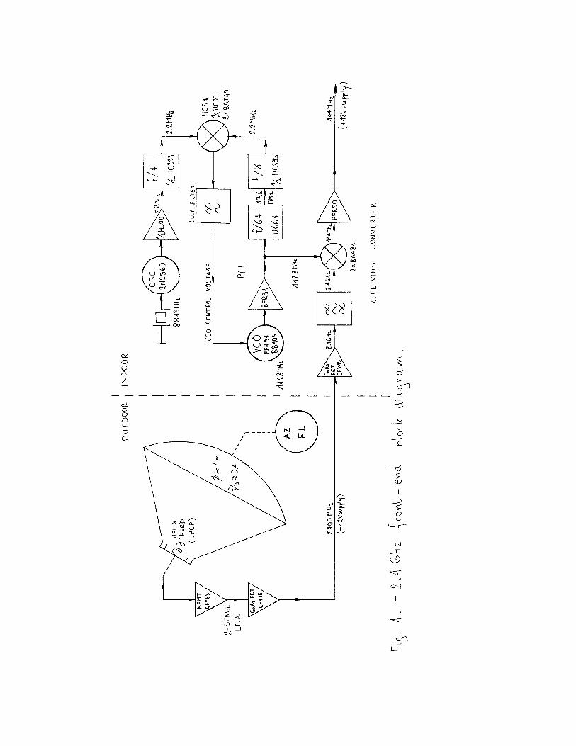
communications are mainly disturbed by military radar in the70cm and 23cm bands and by microwave ovens in the 13cm band.The disturbs from microwave ovens are limited both in theduration and in the daytime they are likely to appear.According to my own experience, the disturbs originating froma microwave oven are efficiently neutralized by a conventionalSSB-receiver "noise-blanker" circuit. The only drawback of using microwave frequencies forsatellite communications is the increased Doppler shift whencompared to VHF or UHF. The quickly-changing Doppler shift isa nuisance especially with low-Earth-orbit satellites whileit is tolerable with high-orbit satellites like AO-13 orARSENE. Using more appropriate types of modulation, likeFM in place of SBB or appropriate digital modulations onecould easily overcome the drawback of the increased Dopplershift even with low-Earth-orbit satellites. Unfortunately, most of the amateur equipment actuallyavailable for 2.4GHz seems both far too complex and perhaps ofobsolete design. The reason for this is probably that 13cmequipment was developed out of existing 23cm equipment, whilethe same 23cm equipment was developed out of even earlier 70cmequipment and so on. This has lead to poor technical solutions,using inappropriate components, that are both complex andunreliable. Therefore I tried to find a simple, easilyreproducible receiver front-end design for 2.4GHz and theresults of these experiments are shown in this article. In this article I am going to describe a complete 2.4GHzreceiving front-end as shown on Fig. 1. The 2.4GHz receiverincludes a suitable antenna installed on an azimuth &elevation rotator, a low-noise antenna amplifier, a receivingdownconverter and a 144MHz (first IF) SSB receiver ortransceiver. To minimize any degradation of the noise figure,the LNA is installed directly on the antenna. On the otherhand, thanks to the LNA, the receiving downconverter may beinstalled anywhere between the LNA and the 144MHz receiver.Both the LNA and the downconverter receive the supply voltagethrough the signal cable to simplify the interconnections.
2. Antenna for 2.4GHz satellite reception----------------------------------------- In all satellite communications it is always desirableto have a very sensitive receiver in the ground station.In this way the minimum amount of transmitter power can beused and the same satellite transponder can be used by a largenumber of stations at the same time. The receiver sensitivitycan be improved using a larger antenna, but the latter ismore expensive and also requires a more powerful, more accurateand faster antenna rotator. To receive radio-amateur satellites in the 2.4GHz band,a reasonable choice is an antenna with a diameter between 80cmand 1m. Such an antenna can still be carried and steered by aconventional amateur antenna rotator (like a Kenpro KR5600),the antenna beam is still wide enough for the mechanicalinaccuracies of cheap antenna rotators and the rotation speedof these rotators is still fast enough to allow the trackingof low-Earth-orbit satellites. The reception of currently

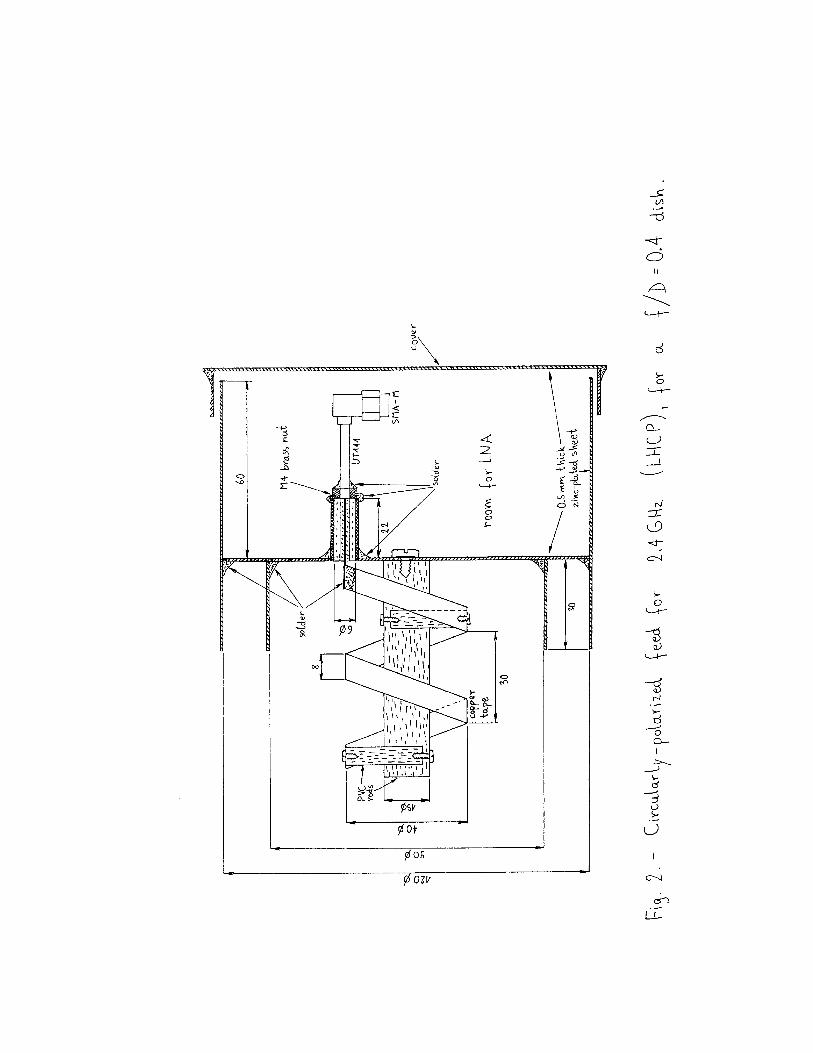
active satellites (AO-13, PACSAT-1 and DOVE-1) is possiblewith even smaller antennas and less sensitive receivers.In the future even more powerful 2.4GHz satellite beacons andtransponders are expected. A reflector antenna, like a parabolic dish with anappropriate feed, usually becomes practical when the requiredantenna diameter exceeds 4 or 5 wavelengths. Slow-wavestructure antennas like Yagis or helices are only practicalfor smaller antenna gains. Considering the problem ofcorrectly feeding a larger number of smaller antennas in the2.4GHz band and the unwanted side lobes of such an array thatdegrade the antenna noise temperature, a reflector antennabecomes practical at a diameter of around 50cm. A parabolic reflector that is accurate enough for 2.4GHzoperation can be manufactured at home by screwing or rivetingtogether a number of aluminum sheet petals. On the other hand,parabolic dishes in the range between 80cm and 1m diameterare easily available on the market for 12GHz satellite TVreception. Since future amateur satellites are also going touse higher frequencies up to 10GHz or 24GHz, I recommend acommercially-made dish due to its better surface accuracy. Parabolic dishes of the same size may look quitedifferent. Besides the dish diameter there is yet anotherimportant parameter of a dish: the focal-to-diameter (f/D)ratio. Commercially available dishes for satellite TVusually fall into two categories: symmetrical "deep" disheswith a f/D around 0.4 and unsymmetrical "flat" dishes withan "offset" feed and a f/D around 0.7. For the operationat 2.4GHz I recommend a conventional symmetrical "deep" dishwith a f/D=0.4, since it is easier to build the correspondingfeed for the operation at 2.4GHz. The polarization of a reflector antenna dependsexclusively on the feed used. Since the position of asatellite is continuously changing with respect to aground station, circular polarization is frequently used insatellite communications. Most amateur satellites useright-hand circular polarization (RHCP). When building acircularly-polarized antenna one should consider that thesense of a circularly polarized wave is inverted on eachreflection. A reflector antenna including a single reflectortherefore requires a LHCP feed to produce a RHCP wave in thefar field! A simple circularly-polarized feed is shown on Fig. 2.The feed shown on Fig. 2 is suitable for a "deep" dish witha f/D=0.4. The feed includes a short two-turn helix with itsown reflector, an impedance-matching transformer and aweather-proof box for the LNA to be installed as close to thefeed as possible. The helix itself is made of 8mm wide copper tape,supported by insulating rods (PVC or better teflon). Thesupporting rods are bolted together with self-locking screws.To avoid disturbing the operation of the helix, the rodsshould be of the smallest practical cross section and the screwsshould be as short as possible. The helix operates as anend-fire antenna and in this operating mode the polarizationcorresponds to the sense of the winding: LHCP is obtained by
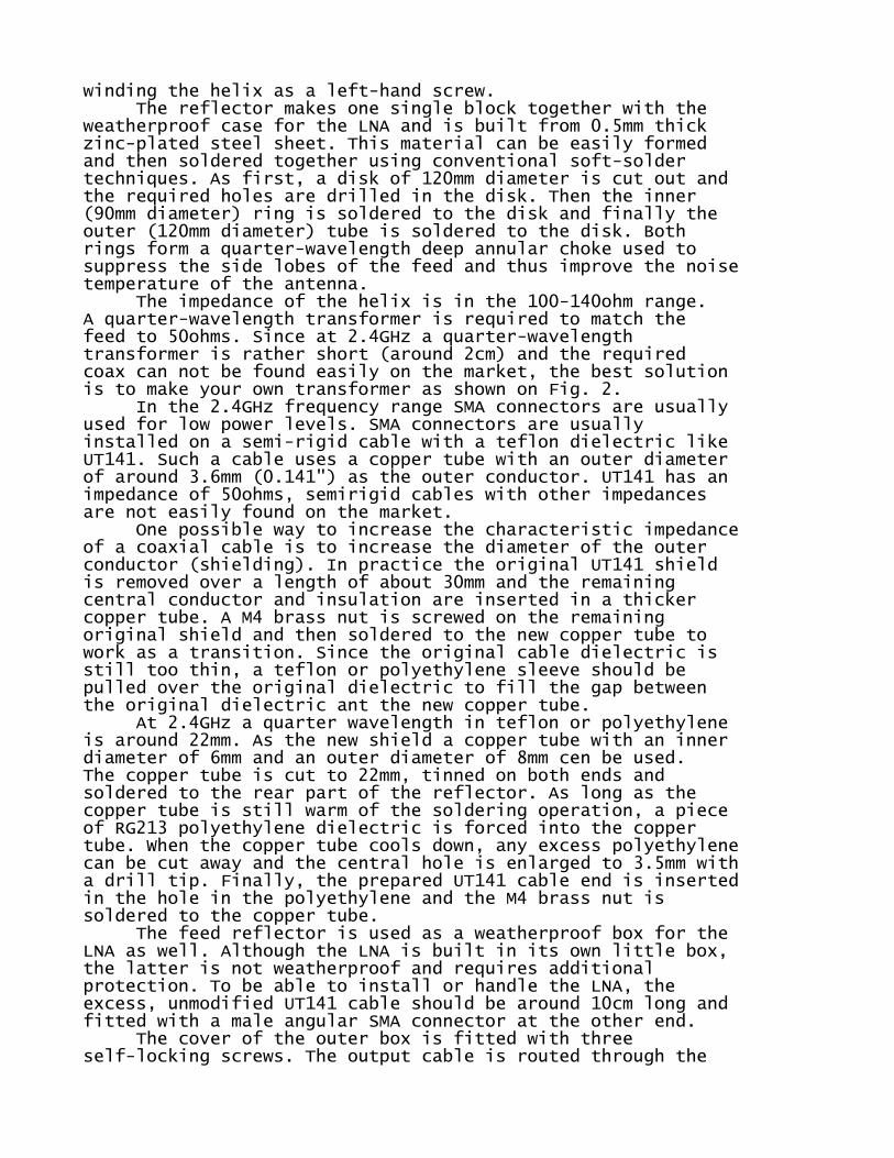
winding the helix as a left-hand screw. The reflector makes one single block together with theweatherproof case for the LNA and is built from 0.5mm thickzinc-plated steel sheet. This material can be easily formedand then soldered together using conventional soft-soldertechniques. As first, a disk of 120mm diameter is cut out andthe required holes are drilled in the disk. Then the inner(90mm diameter) ring is soldered to the disk and finally theouter (120mm diameter) tube is soldered to the disk. Bothrings form a quarter-wavelength deep annular choke used tosuppress the side lobes of the feed and thus improve the noisetemperature of the antenna. The impedance of the helix is in the 100-140ohm range.A quarter-wavelength transformer is required to match thefeed to 50ohms. Since at 2.4GHz a quarter-wavelengthtransformer is rather short (around 2cm) and the requiredcoax can not be found easily on the market, the best solutionis to make your own transformer as shown on Fig. 2. In the 2.4GHz frequency range SMA connectors are usuallyused for low power levels. SMA connectors are usuallyinstalled on a semi-rigid cable with a teflon dielectric likeUT141. Such a cable uses a copper tube with an outer diameterof around 3.6mm (0.141") as the outer conductor. UT141 has animpedance of 50ohms, semirigid cables with other impedancesare not easily found on the market. One possible way to increase the characteristic impedanceof a coaxial cable is to increase the diameter of the outerconductor (shielding). In practice the original UT141 shieldis removed over a length of about 30mm and the remainingcentral conductor and insulation are inserted in a thickercopper tube. A M4 brass nut is screwed on the remainingoriginal shield and then soldered to the new copper tube towork as a transition. Since the original cable dielectric isstill too thin, a teflon or polyethylene sleeve should bepulled over the original dielectric to fill the gap betweenthe original dielectric ant the new copper tube. At 2.4GHz a quarter wavelength in teflon or polyethyleneis around 22mm. As the new shield a copper tube with an innerdiameter of 6mm and an outer diameter of 8mm cen be used.The copper tube is cut to 22mm, tinned on both ends andsoldered to the rear part of the reflector. As long as thecopper tube is still warm of the soldering operation, a pieceof RG213 polyethylene dielectric is forced into the coppertube. When the copper tube cools down, any excess polyethylenecan be cut away and the central hole is enlarged to 3.5mm witha drill tip. Finally, the prepared UT141 cable end is insertedin the hole in the polyethylene and the M4 brass nut issoldered to the copper tube. The feed reflector is used as a weatherproof box for theLNA as well. Although the LNA is built in its own little box,the latter is not weatherproof and requires additionalprotection. To be able to install or handle the LNA, theexcess, unmodified UT141 cable should be around 10cm long andfitted with a male angular SMA connector at the other end. The cover of the outer box is fitted with threeself-locking screws. The output cable is routed through the

side (cylindrical) wall of the outer box. Experience has shownthat any "waterproof" enclosure is a very efficient moisturecollector, so rather than a watertight box I recommend aventilation hole positioned so that it always looks down,even when the antenna is turned in azimuth and elevation.
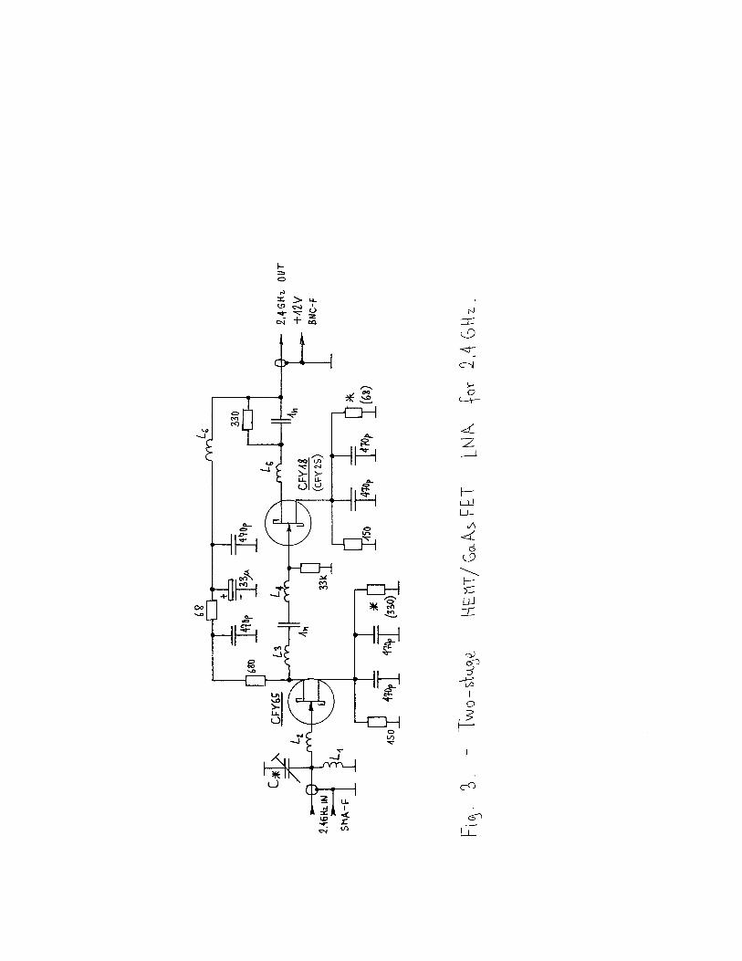
3. Two-stage HEMT/GaAsFET LNA for 2.4GHz---------------------------------------- The usual amateur procedure to design and build amicrowave low-noise preamplifier includes the selection ofthe active devices based on cost and availability rather thanelectrical performances and the design of an (un)suitablemicrostrip circuit based on extensive computations.Unfortunately very little experimentation has been done withthe real amplifier circuit and even less experiments have beenmade to use other construction techniques than microstrip. Most of the available GaAs FETs and improved devices likeHEMTs have been designed for operation at 12GHz in a 50ohmenvironment in a microstrip circuit of satellite-TVdownconverter. The same devices can offer even betterperformances at lower frequencies. However, if one wants tomake use of the improved device performance at 2.4GHz, thedevices have to be accurately matched to much higherimpedances than 50ohms. The required impedance transformationsrequire very narrow microstrip lines or other more complexmicrostrip circuits and all of these are very lossy even onhigh-quality teflon printed-circuit boards. From the above it is clear that microstrip is not asuitable technology to build a 2.4GHz LNA with conventionalGaAsFETs. Further, at lower frequencies, GaAsFET amplifiersmay have stability problems and a careful design of theamplifier matching and bias networks is required. Finally,there are a few practical considerations, like overloadproblems from very strong out-of-band signals, like theground-station's own uplink transmitter. The design of the LNA for 2.4GHz is based on a verysuccesful design of a two-stage GaAsFET LNA for L-band(1000MHz - 1700MHz), already published in UKW-Berichte(VHF-Communications) 3/1991, pages 163-169. Two stages provideenough gain to overcome the losses in the cable to the indoorreceiving downconverter. Rather than using microstriptechnology, the LNA is built using air lines that have muchhigher characteristic impedances and even lumped components.Suitable line impedances enable very low-loss impedancetransformations resulting in a very low overall noise figureof less than 0.4dB when using a CFY65 HEMT in the first stage. The circuit diagram of the two-stage HEMT/GaAsFET LNAfor 2.4GHz is shown on Fig. 3. Matching a GaAsFET to a 50ohmenvironment can be achieved easily using series inductorsat 2.4GHz. Only a few if any additional components arerequired, like the input capacitor C*. The series inductorsare simply short pieces of silver-plated wire or componentleads. Such matching circuits have one or two orders ofmagnitude smaller losses than an equivalent microstripcircuit! Since the parasitics are mainly capacitances, a GaAsFET

amplifier stage will only oscillate at low frequencies if boththe input and the output are terminated into inductive loadswith sufficiently high Qs. In a two-stage amplifier stabilitycan be achieved with a carefully designed interstage matchingnetwork. In particular, in a two-stage GaAsFET amplifier anyinductors or RF chokes towards ground or supply rails shouldbe avoided in the interstage matching network, since they mayrepresent a high-Q inductor at some frequency, sometimes faraway from the designed operating frequency of the amplifier. The 2.4GHz LNA is built in a small box made of 0.5mmthick brass sheet (see Fig. 4), which is 50mm long, 20mm wideand 15mm high. The box is small enough to prevent resonancesbelow 7GHz. However, HEMTs are able to oscillate at much higherfrequencies too. Such oscillations are difficult to detectsince the other semiconductors used in the receiver are notable to detect nor to convert these spurious signals tolower frequencies. HEMT oscillations above 10 or 15GHz aretherefore only observed as amplifier gain variations whenthe box is closed. Of course the solution for theseoscillations is a piece of microwave absorber (black"antistatic" foam) positioned over the second stage to avoiddegrading the noise figure at 2.4GHz. For operation at 2.4GHz a female SMA connector should beused on the input while a female BNC (UG1094) is still goodenough on the output. Of course inexpensive connectors forcomputer networks are to be strictly avoided! Both connectorsare soldered to the LNA box to minimize the parasitics. Oneshould also avoid to use "CB quality" RG58 cable to connectthe LNA to the downconverter. Much better choices are RG223(double shield, silver plated) or RG142 (teflon dielectric)or RG214 (for longer cable runs). The whole LNA circuit is supported by six leadlessceramic disc capacitors. The nominal value of these capacitors(470pF) is unimportant. It is much more important to useonly single-layer ceramic leadless capacitors, of either round(disc) or trapezoidal shape. When soldering these capacitorsone should take care to add enough solder between thecapacitor metalization and the brass sheet bottom to ensuregood solder wetting and prevent the cracking of the brittlecapacitor due to case sheet bending. WARNING! Avoid usingthe so called "chip" or "SMD" multilayer capacitors, thatbehave in strange way at microwave frequencies. The two interstage coupling capacitors (1nF) areconventional ceramic disc capacitors with wire leads. Theparasitic inductance of the leads of these capacitors isactually forming the inductors L3, L4 and L5. The 33uFtantalum capacitor is used to suppress any spikes on thesupply rail that could damage the microwave semiconductors.All of the resistors are conventional 1/8W resistors withwire leads. The resistors marked with a "*" are adjusted forthe correct bias of the two FETs. The quarter wavelength chokes L1 and L6 are made out of4cm of 0.15mm thick enameled copper wire. The piece of wireis first tinned for about 5mm at each end, the untinned part isthen wrapped around an 1mm drill tip to obtain a coil, theactual number of turns being unimportant.
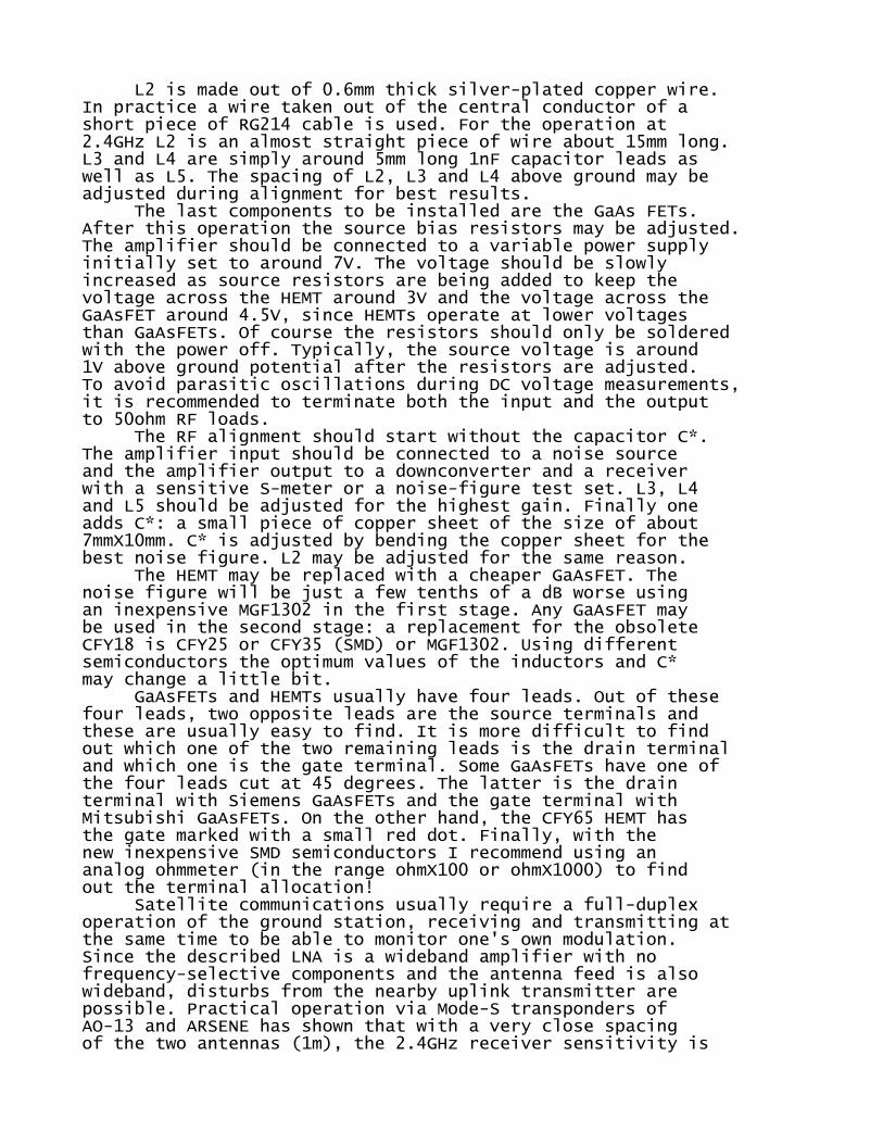
L2 is made out of 0.6mm thick silver-plated copper wire.In practice a wire taken out of the central conductor of ashort piece of RG214 cable is used. For the operation at2.4GHz L2 is an almost straight piece of wire about 15mm long.L3 and L4 are simply around 5mm long 1nF capacitor leads aswell as L5. The spacing of L2, L3 and L4 above ground may beadjusted during alignment for best results. The last components to be installed are the GaAs FETs.After this operation the source bias resistors may be adjusted.The amplifier should be connected to a variable power supplyinitially set to around 7V. The voltage should be slowlyincreased as source resistors are being added to keep thevoltage across the HEMT around 3V and the voltage across theGaAsFET around 4.5V, since HEMTs operate at lower voltagesthan GaAsFETs. Of course the resistors should only be solderedwith the power off. Typically, the source voltage is around1V above ground potential after the resistors are adjusted.To avoid parasitic oscillations during DC voltage measurements,it is recommended to terminate both the input and the outputto 50ohm RF loads. The RF alignment should start without the capacitor C*.The amplifier input should be connected to a noise sourceand the amplifier output to a downconverter and a receiverwith a sensitive S-meter or a noise-figure test set. L3, L4and L5 should be adjusted for the highest gain. Finally oneadds C*: a small piece of copper sheet of the size of about7mmX10mm. C* is adjusted by bending the copper sheet for thebest noise figure. L2 may be adjusted for the same reason. The HEMT may be replaced with a cheaper GaAsFET. Thenoise figure will be just a few tenths of a dB worse usingan inexpensive MGF1302 in the first stage. Any GaAsFET maybe used in the second stage: a replacement for the obsoleteCFY18 is CFY25 or CFY35 (SMD) or MGF1302. Using differentsemiconductors the optimum values of the inductors and C*may change a little bit. GaAsFETs and HEMTs usually have four leads. Out of thesefour leads, two opposite leads are the source terminals andthese are usually easy to find. It is more difficult to findout which one of the two remaining leads is the drain terminaland which one is the gate terminal. Some GaAsFETs have one ofthe four leads cut at 45 degrees. The latter is the drainterminal with Siemens GaAsFETs and the gate terminal withMitsubishi GaAsFETs. On the other hand, the CFY65 HEMT hasthe gate marked with a small red dot. Finally, with thenew inexpensive SMD semiconductors I recommend using ananalog ohmmeter (in the range ohmX100 or ohmX1000) to findout the terminal allocation! Satellite communications usually require a full-duplexoperation of the ground station, receiving and transmitting atthe same time to be able to monitor one's own modulation.Since the described LNA is a wideband amplifier with nofrequency-selective components and the antenna feed is alsowideband, disturbs from the nearby uplink transmitter arepossible. Practical operation via Mode-S transponders ofAO-13 and ARSENE has shown that with a very close spacingof the two antennas (1m), the 2.4GHz receiver sensitivity is

degraded at 435MHz transmitter power levels above 5W. Thanksto the very variable power of SSB modulation and thepropagation delay one can thus easily monitor his ownmodulation.
4. Receiving downconverter for 2.4GHz------------------------------------- A large number of receiving downconverters for amateurmicrowave frequency bands has been described in the literaturein the last 10 or 15 years. On the other hand, all of thedescribed downconverters are very similar, just like thetechnology did not make any progress in the last 15 years.All of the described downconverters have a GaAsFET on theinput, a crystal oscillator somewhere between 80 and 110MHz,an "infinitely" long chain of frequency-multiplier stages,some filters made in microstrip technology and finally a mixerwith Schottky diodes or yet another GaAsFET. Such converter designs have several weak points. Thefirst is the crystal oscillator. Above 80MHz the fifthovertone resonance has to be used although the crystal itselfis thinner than 0.1mm. Thin crystals suffer a faster agingand break quickly from a mechanical shock. On the other hand,the operation of a crystal oscillator at the 5th overtoneresonance is usually far from reliable. Frequency-multiplier stages are even worse. Using vacuumtubes or bipolar transistors one can build simple and reliablemultiplier stages up to perhaps 500MHz. Above this frequencyharmonics are mainly generated by the collector-base junctionvaractor in a bipolar transistor. The operation of a varactoror step-recovery-diode multiplier requires much higher signallevels, close to the destruction levels for the transistorsused as frequency multipliers. The operation of suchmultiplier stages is of course quite unreliable, thetransistors may fail or just degrade their performances aftersome time and very seldom one is able to reproduce the circuitand achieve the same electrical performances as mentioned bythe author in his original article. Finally, most downconverter designs use high-Q circuits,tuned with unsuitable trimmers, both in the multiplier chainand in the RF stages. Tuning such a downconverter requiresa large amount of both patience and instrumentation.Unfortunately, the tuning has to be performed once again afterany shocks applied to the downconverter or even after widetemperature excursions. Of course it makes sense to look at alternate designs.Together with the introduction of satellite TV, inexpensivesingle-chip PLL synthesizers appeared on the market forfrequencies up to 1.5GHz or even 2.5GHz. One of the firstdevices was the Siemens SDA3202, now there are many similarchips produced by different manufacturers. The SDA3202 wassuccessfully used by amateurs in wideband transmitters andreceivers, like FM ATV on the 23cm band. Unfortunately thesesingle-chip synthesizers are not suitable for SSB convertersor transverters, since the division modulos are too large andthe PLL gain is too low. Simply speaking, such a PLL is tooslow to stabilize quick random variations of the VCO frequency

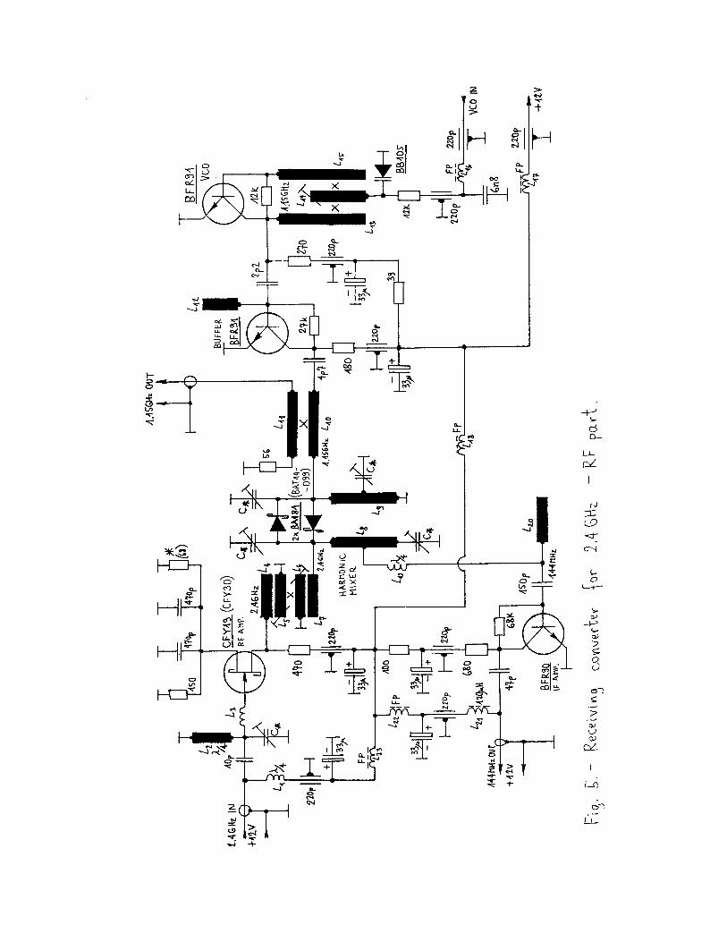
for SSB or CW narrowband operation. A synthesizer for a SSB microwave converter thereforehas to be built from a number of digital integrated circuits,to avoid the unreliable frequency-multiplier chain. The blockdiagram of the receiving converter for 2.4GHz was alreadyshown on Fig. 1. The detailed circuit diagram is shown onFig. 5 and Fig. 6: the RF part on Fig. 5 and the PLL logicon Fig. 6. The receiving converter includes a RF amplifier stagewith a CFY19 GaAsFET, a harmonic mixer with two schottkydiodes BA481 and an IF amplifier stage with a BFR90. Thesynthesizer produces a signal at 1128MHz, since the harmonicmixer generates itself the second harmonic at 2256MHz asrequired for the downconversion from 2400MHz to 144MHz.The synthesizer includes a VCO operating at 1128MHz (BFR91 andBB105), a buffer stage (BFR91), a fast ECL prescaler U664,some additional dividers (74HC393), a 9MHz crystal oscillatorand a frequency/phase comparator (74HC74 and 74HC00). The input RF amplifier with the GaAsFET CFY19 is requiredto overcome the losses in the 2.4GHz bandpass filter (L4, L5,L6 and L7) and mask the high noise figure of the harmonicmixer. The latter is using two antiparallel diodes to convertthe incoming RF signal with the second harmonic of the localoscillator. Since the input RF frequency (2.4GHz) and thelocal oscillator frequency (1128MHz) are in an approximateratio of 2:1, the mixer circuit results very simple andrequires just two resonant microstrips (L8 and L9). The latterare dimensioned to represent a quarter wavelength for the VCOfrequency and a half wavelength for the input RF signal. Harmonic mixers require very good mixer diodes, since thesame diodes provide both the frequency doubling and inputsignal conversion. Common Schottky diodes like BA481, HP2900or similar are not very suitable for this application and theresult is a rather high noise figure of the mixer alone inthe range between 12 and 15dB. Including the losses in the2.4GHz bandpass and the gain and noise of the CFY19, theoverall downconverter noise figure is in the 6 to 7dB range. Much better results can be obtained using new componentslike the Ku-band double Schottky diode BAT14-099 (SMD plasticpackage): the mixer noise figure drops down to only 6-7dB andthe overall downconverter noise figure down to only 3dB! The mixer is followed immediately by an IF amplifierstage (BFR90), so that even a "deaf" 144MHz IF receiver canno longer spoil the downconverter noise figure. The IFamplifier does not include any tuned circuits, since noselectivity is required. Since there are no multiplier stages,there are also no spurious frequencies that could disturbthe operation of the IF amplifier or even bring the IF stageinto saturation. There is just a low-pass filter on the input(L19 and L20) to reject the VCO signal at 1128MHz. The downconverter receives the required supply voltagethrough its output IF coaxial connector. On the other hand,the downconverter supplies the LNA with the same supplyvoltage through its input RF coaxial connector. All thissimplifies the installation, since there are no additionalsupply cables.

A SSB synthesizer requires a VCO with a top phase-noiseperformance. The VCO includes an amplifier stage (BFR91) andan interdigital bandpass filter (L13, L14 and L15) feedback.The VCO frequency is adjusted by tuning the central finger(L14) of the interdigital filter with the varicap diode BB105.The latter can shift the VCO frequency by about 10% of thecentral operating frequency. The real tuning range is furtherrestricted by the control voltage between 0 and 5V. The operation of the described VCO is so stable that theVCO supply voltage does not need to be stabilized. The VCO isfollowed by a buffer stage with another BFR91. The bufferedVCO signal is then fed to the harmonic mixer through a couplerand a small amount of the VCO signal power (about 1%) is fedto the input of the ECL prescaler U664. The coupler alsoallows a wideband termination (56ohm resistor) for theprescaler input. The PLL divider should operate reliably up to the maximumVCO frequency of about 1200MHz. A fast ECL divider istherefore required for the first divider stages. Theintegrated circuit U664 includes an input signal preamplifierand chain of 6 flip-flops with no feedback, so that theoverall division modulo is equal to 64. The output frequencyof the U664 prescaler is around 17.6MHz. This frequency isstill too high for the frequency/phase comparator and furtherdivision is necessary. In a PLL synthesizer for a SSB converter the smallestpossible division ratios and the highest comparison frequencyare desired to speed-up the PLL and reduce the phase noise ofthe VCO. The main limitation is the frequency/phase comparator.The most popular circuit is the charge-pump comparator and thelatter is limited to about one tenth of the maximum clockfrequency of the logic family used. Since 74HCxx family logiccircuits have a maximum clock frequency of about 40MHz, thehighest practical comparison frequency is around 4MHz. The prescaler output signal is therefore further dividedby 8 by one half of the 74HC393 while the second half of thesame chip is used to divide the frequency of the referencecrystal oscillator. The comparison frequency is around 2.2MHzto operate the circuit with a considerable safety margin.The output of the frequency/phase comparator is a charge-pumpcircuit with two fast Schottky diodes BAT47, allowing anoutput voltage swing from about 0.5V up to 4.5V. Most charge-pump frequency/phase comparators have ahysteresis or backlash problem. The latter may be a majorsource of phase noise in a PLL frequency synthesizer. In thedescribed circuit, the backlash problem is solved by havingthe charge-pump circuit (diodes BAT47) faster than thefeedback network (1/4 74HC00, pins 8,9,10) to the twoD-flip-flops. The response of such a comparator is stillnonlinear around the locking point, but the backlash problemis eliminated, resulting in an excellent synthesizer frequencystability. The receiving downconverter for 2.4GHz is alsopractically built as two separate modules. The RF part isbuilt on a two-sided printed-circuit board in microstriptechnology, of the size of 120mmX40mm, as shown on Fig. 7.
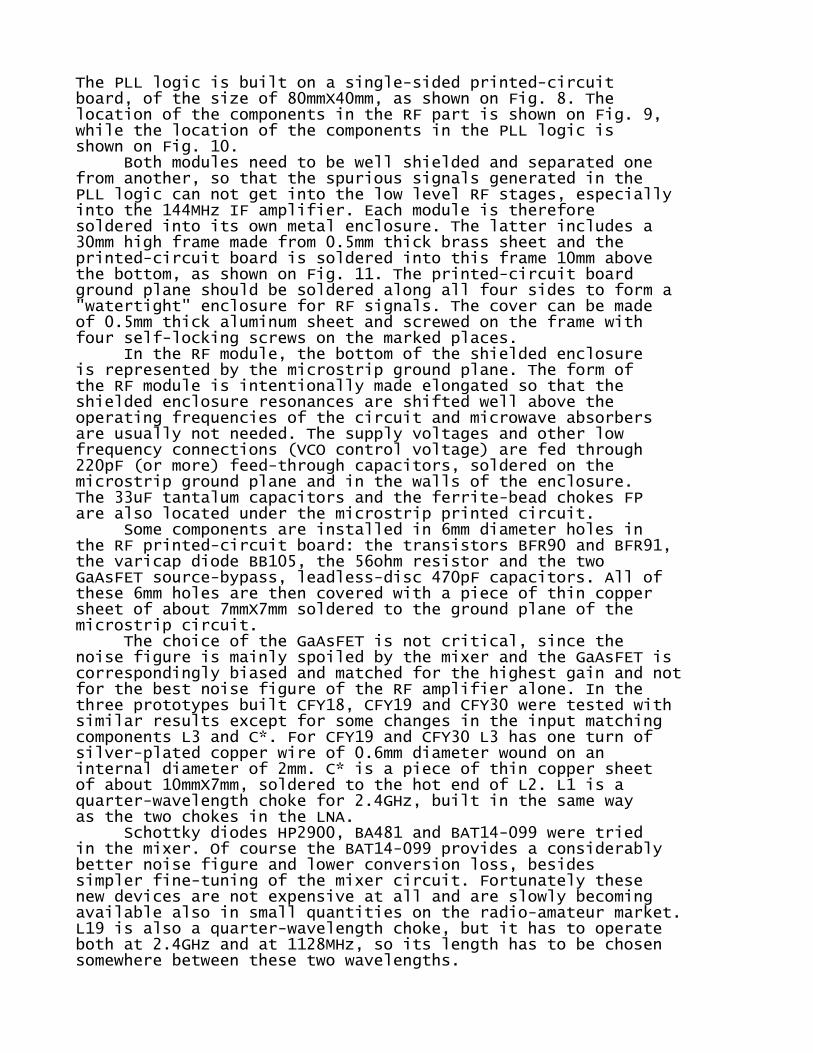
The PLL logic is built on a single-sided printed-circuitboard, of the size of 80mmX40mm, as shown on Fig. 8. Thelocation of the components in the RF part is shown on Fig. 9,while the location of the components in the PLL logic isshown on Fig. 10. Both modules need to be well shielded and separated onefrom another, so that the spurious signals generated in thePLL logic can not get into the low level RF stages, especiallyinto the 144MHz IF amplifier. Each module is thereforesoldered into its own metal enclosure. The latter includes a30mm high frame made from 0.5mm thick brass sheet and theprinted-circuit board is soldered into this frame 10mm abovethe bottom, as shown on Fig. 11. The printed-circuit boardground plane should be soldered along all four sides to form a"watertight" enclosure for RF signals. The cover can be madeof 0.5mm thick aluminum sheet and screwed on the frame withfour self-locking screws on the marked places. In the RF module, the bottom of the shielded enclosureis represented by the microstrip ground plane. The form ofthe RF module is intentionally made elongated so that theshielded enclosure resonances are shifted well above theoperating frequencies of the circuit and microwave absorbersare usually not needed. The supply voltages and other lowfrequency connections (VCO control voltage) are fed through220pF (or more) feed-through capacitors, soldered on themicrostrip ground plane and in the walls of the enclosure.The 33uF tantalum capacitors and the ferrite-bead chokes FPare also located under the microstrip printed circuit. Some components are installed in 6mm diameter holes inthe RF printed-circuit board: the transistors BFR90 and BFR91,the varicap diode BB105, the 56ohm resistor and the twoGaAsFET source-bypass, leadless-disc 470pF capacitors. All ofthese 6mm holes are then covered with a piece of thin coppersheet of about 7mmX7mm soldered to the ground plane of themicrostrip circuit. The choice of the GaAsFET is not critical, since thenoise figure is mainly spoiled by the mixer and the GaAsFET iscorrespondingly biased and matched for the highest gain and notfor the best noise figure of the RF amplifier alone. In thethree prototypes built CFY18, CFY19 and CFY30 were tested withsimilar results except for some changes in the input matchingcomponents L3 and C*. For CFY19 and CFY30 L3 has one turn ofsilver-plated copper wire of 0.6mm diameter wound on aninternal diameter of 2mm. C* is a piece of thin copper sheetof about 10mmX7mm, soldered to the hot end of L2. L1 is aquarter-wavelength choke for 2.4GHz, built in the same wayas the two chokes in the LNA. Schottky diodes HP2900, BA481 and BAT14-099 were triedin the mixer. Of course the BAT14-099 provides a considerablybetter noise figure and lower conversion loss, besidessimpler fine-tuning of the mixer circuit. Fortunately thesenew devices are not expensive at all and are slowly becomingavailable also in small quantities on the radio-amateur market.L19 is also a quarter-wavelength choke, but it has to operateboth at 2.4GHz and at 1128MHz, so its length has to be chosensomewhere between these two wavelengths.
Suitable ECL prescalers are available from manymanufacturers, since these devices were used in TV tunersa few years ago. The Telefunken U664 seems to be the easiestto get as a TV replacement part. The circuit also works withthe Siemens SDA2101, which has a lower frequency limit anda less sensitive input. Unfortunately the SDA2211 could notbe tested since unavailable, although this circuit probablyhas the best RF performance (1.8GHz) and lower powerconsumption. All of the mentioned ECL prescalers are packagedin the same 8-pin package and are pin compatible. The PLL logic is built in a similar metal enclosure,although because of a single-sided board the enclosure doesnot have a shielded bottom. The feed-through capacitors areonly built in the enclosure walls. The 7805 regulator (TO220version) is bolted to the brass frame for heat sinking.The only remaining critical component are the charge-pumpdiodes. These must be Schottky diodes for speed reasons, toavoid backlash problems in the frequency/phase comparator.General purpose switching Schottky diodes like BAT47, HSCH1001or similar devices are suitable for this purpose. The checkout and alignment of the downconverter shouldstart with the selection of the reference crystal. Since mostof the amateur-radio satellites operate in the subband2400.000MHz to 2402.000MHz, it makes sense to convert thisfrequency band to 144-146MHz using a local oscillator at2256MHz. The latter frequency requires a crystal for8812.5kHz in the PLL. Only ARSENE operates at a higherfrequency around 2446.5MHz. To convert its signal to 144.5MHz,a local oscillator at 2302MHz is required. The latter needs acrystal for 8992.19kHz in the PLL. Both required crystals can be found among standardCitizen-Band radio crystals, of course operated on theirfundamental resonance. For 8812.5kHz one can use the CBchannel #1 RX crystal (26.510MHz) that resonates around8837kHz in its fundamental mode. The crystal frequency isstill about 24kHz too high, but fortunately the fundamentalresonance of a crystal can be easily shifted downwards witha series inductor (L*). Due to the relatively largefrequency shift required, the value of L* is also quite large,up to 30uH, and some experimenting is necessary in any case. On the other hand, it is much easier to obtain 8992.19kHzfrom a CB channel #2 TX crystal (26.975kHz), that usuallyrequires just minor frequency adjustments either with aseries inductor L* or with a series trimmer capacitor, butnever both at the same time! When using inexpensive CBcrystals one should always check that the oscillator operatesreliably on a single crystal mode. For better frequencystability the CB crystals should be replaced with custom-madecrystals, specified for a series resonance at the desiredfrequency and fine-tuned with a small series inductor L*. In the next step the complete PLL should be assembledand the VCO should be checked out. The operation of the VCOcan be observed as a DC voltage decrease on both BFR91 bases,of course measured through suitable RF chokes. The VCO shouldbe fine-tuned by adjusting the length of L14. Usually L14 hasto be made a little longer by adding a small piece of copper
foil on its hot end (towards the transistor BFR91). L14 shouldbe adjusted to obtain a PLL control voltage of 2.5V in thelocked state of the PLL. When the PLL achieves lock, the pulseson LOCK T.P. become very narrow and the DC voltage componentapproaches zero. Even this voltage should only be checkedthrough a RF choke, since conventional AVO meters usuallybehave in a crazy way with a RF of just 2.2MHz applied totheir terminals! Once the PLL operates reliably, the GaAsFET is solderedin the circuit and its source bias resistors are adjusted justlike in the LNA. Then a noise source should be connected tothe input of the downconverter and a receiver with a sensitiveS-meter to the output. All of the following adjustments aresimply made for the highest gain or the strongest signal onthe S-meter. The first thing to check is whether the receiveris able to hear the noise source at all! Next the RF inputmatch should be optimized by changing C*: moving and bendingthe small piece of copper sheet. When the RF input match is optimized one can startworking on the harmonic mixer. In the latter L8 and L9 canbe optimized by adding small pieces of copper foil (about7mmX7mm) in different places along these two resonant lines.The optimum position and size of these pieces of copper foildepend very much on the diodes used in the mixer. Suitablediodes like BAT14-099 usually require little tuning, but onthe other hand it is much more difficult to obtain a decentnoise figure out of BA481 or HP2900 diodes. Finally the 2.4GHz bandpass may be optimized by adjustingthe length of L5 and L6. These two resonators are howeveralready adjusted to the correct length and hardly require anyadditional adjustments, at least if their cold ends arecorrectly grounded using a 1mm diameter copper wire tointerconnect both sides of the microstrip board. If adjustingL5 or L6, proceed very carefully and never add or remove morethan 0.5mm at a time! In any case, these microstrip resonatorsdo not have a particularly high Q, especially since the boardmaterial is lossy, 1.6mm thick glassfiber-epoxy.
5. Assembly of a 2.4GHz receiving ground station------------------------------------------------ At the end of this article I find it necessary to spenda few words about the assembly of a ground station from thecomponents already described. The single components are notnecessarily built in the same order as described in thisarticle, nor all of them may not be required in a particulargroundstation. Using better components in the downconverterone could avoid the LNA or alternatively use a much smallerantenna, like a long helix. Both the LNA and the receiving downconverter are designedto get the supply voltage through the same RF cables. The LNAreceives its supply voltage through its output connectorwhile the downconverter has the supply voltage on both RFconnectors. In this way all of the system components areconnected with a single RF cable and this is usually verypractical when making a practical installation on the roofor on the antenna tower.
As a 144MHz IF receiver radio amateurs usually use a2m SSB transceiver. SSB transceivers usually do not haveavailable the supply voltage on the RF connector. In additionit is very easy to destroy a receiving downconverter connectedto a transceiver, if the latter is accidentally switched totransmission. Therefore I recommend a protected supply circuitfor the downconverter as shown on Fig. 12. This simple circuitcan be built in a small metal box and the few componentssoldered directly among the three connectors. The circuitintroduces some RF signal loss because of the 33ohm resistor,but on the other hand this resistor protects both thedownconverter and the transmitter if the latter isaccidentally enabled. The 33ohm resistor is rated at 1/2Wpower dissipation and this should be enough for shortoverloads, although in both my prototypes these resistorsalready changed their color! If the LNA is omitted, then the downconverter should beinstalled as close as possible to the antenna and the supplyvoltage should be removed from the downconverter input, toavoid shorts in the antenna. On the other hand, when using theLNA, the downconverter can be installed indoor. The LNA gainis sufficient to cover a loss of about 10dB in the cable tothe downconverter corresponding to about 20m of good qualitycable like RG214. An indoor downconverter is less subjected totemperature variations and its frequency is more stable asif it were installed outdoor, directly on the antenna. The whole receiving system as described in this articleprovides a system noise temperature in the range between 60Kand 70K. In other words, if the antenna is turned towards thewarm ground, the noise level should increase by 6 or 7dB.When the antenna is turned towards the cold sky, about halfof the noise is provided by the antenna itself due to the skytemperature and the dish feed spillover collecting warm-groundnoise. The remaining half of the noise power, 30-35K, isthe receiver noise corresponding to an overall noise figurebetween 0.4 and 0.5dB. It is believed that this figurerepresents today the amateur technology limit, but anywaynot much can be gained going beyond due to the natural noisecollected by the antenna. Using a 90cm (3 foot) diameter parabolic dish thedescribed receiving system provides more than 10dB of marginover what is required to receive the currently activesatellites in the 2.4GHz band: AO-16 and DOVE beacons and theAO-13 linear transponder. This margin is very welcome whenthe satellites are in an unfavorable position on the sky withthe antennas oriented away from us. On the other hand thismeans that the above-mentioned satellites can be received withsmaller antennas and even without a LNA at the same time! Weaker signals were only received from UO-11 and ARSENE.UO-11 probably has a defective transmitter that has only beenswitched on on very rare occasions while ARSENE has a low gainS-band antenna. Although the ARSENE signal was 10-15dB belowthe AO-13 signal, the described receiver with a 90cm dishwas sufficient for normal SSB contacts, to listen to my ownSSB echo with just about 500W EIRP on 70cm and even to hearthe ARSENE transponder noise, when the kilowatt stations were

off, of course... At the end, lets hope that P3D and its high-powerS-band transmitter get safely to the desired orbit!
***************************************************************
List of figures:----------------
Fig. 1 - 2.4GHz front-end block diagram.Fig. 2 - Circulary-polarized feed for 2.4GHz (LHCP), for a f/D=0.4 dish.Fig. 3 - Two-stage HEMT/GaAsFET LNA for 2.4GHz.Fig. 4 - 2.4GHz LNA construction and parts layout.Fig. 5 - Receiving converter for 2.4GHz - RF part.Fig. 6 - Receiving converter for 2.4GHz - PLL logic.Fig. 7 - Printed-circuit board for the 2.4GHz converter, RF part, double-sided 1.6mm thick glassfiber-epoxy, top view, the other side is not etched!Fig. 8 - Printed-circuit board for the 2.4GHz converter, PLL logic, single-sided, bottom view.Fig. 9 - 2.4GHz converter, RF part component layout.Fig. 10 - 2.4GHz converter, PLL logic component layout.Fig. 11 - 2.4GHz converter module enclosure.Fig. 12 - Protected supply circuit.