a novel idea of pseudo-code generator in quantum-dot...
TRANSCRIPT

A novel idea of pseudo-code generator in quantum-dot cellularautomata (QCA)
Firdous Ahmad1, M. Mustafa1, Nisar Ahmad Wani1, and Feroz A Mir2,*
1 Department of Electronics & Instrumentation Technology, University of Kashmir, Srinagar 190006, India2 University Science Instrumentation Centre (USIC), University of Kashmir, Srinagar 190006, India
Received 23 June 2013 / Accepted 23 October 2013 / Published online 4 February 2014
Abstract – In present work, we have implemented the pseudo-code (PN-code) generator using quantum-dot cellular(QCA) technology. Simulation results are obtained from QCA designer software. The PN-code generation is of para-mount importance for any secure communication system. The complex code generated is used to scramble incomingplain text. At the receiving end, the same code is generated and successfully used to decrypt the transmitted data. Thealgorithm for generating noise signal is quite simple. The simplicity of the circuit along with the complexity of the codegenerated makes the circuit attractive for secure message communication.
Key words: Generator, Communication, Noise, Technology, Circuit, Algorithm.
1 Introduction
The microelectronics industry has improved the integration,the power consumption, and the speed of integrated circuitsduring past several decades by means of reducing the featuresize of various semiconducting components. But it seems thateven by decreasing the transistor sizes, some problems suchas power consumption cannot be ignored. Utilizing the QCAtechnology for implementing logic circuits is one of theapproach which in addition to decreasing the size of logic cir-cuits and increasing the clock frequency of these circuits,reduces the power consumption of these circuits. QCA whichwas first introduced by Lent et al. [1] represents an emergingtechnology at the nanotechnology level. QCA cells have quan-tum dots, in which the position of electrons will determine thebinary levels of 0 and 1. As an application of QCA technology,we have implemented the pseudo-code generator. In the nextSection, we have explained the quantum dot cellular automata.It includes the cell introduction, cell-cell coupling, QCA logic,and QCA clocking. Section 3 describes the pseudo-code gener-ator. In Section 4, our work is explained and the simulationresults are illustrated. Section 5 concludes the paper. Simulationresults of this implementation are obtained from QCADesignerv2.0.3 software (QCADesigner is developed by the ATIPS labat the University of Calgary in Canada). QCADesigner v2.0.3features different simulation engines. Throughout this paper,
the Bistable approximation engine is used due to its accurateand detailed evaluation of QCA.
2 Quantum-dot cellular automata
Fundamental unit of QCA device is QCA cell. QCA cellessential consists of four quantum dots arranged in square pat-tern coupled by tunneling barriers as shown in Figure 1a. Quan-tum dots are nano meter sized structures that is capable oftrapping electrons in three dimensions. Due to Coulombicrepulsion, the two electrons reside in opposite corners repre-senting two polarizations [2]. Here we associate P = �1 repre-sents binary ‘‘0’’, P = +1 represents binary ‘‘1’’. Figures 1a and1b shows how one cell is affected by the state of its neighbor. Itshows how the polarization of cell 2 (P2) is determined by thepolarization of its neighbor (P1). P1 is assumed to be fixed at agiven value, corresponding to a specific arrangement of chargesin cell 1 and this charge distribution exerts its influence on cell2, and hence determining its polarization. The results which canbe drawn here is the strongly non-linear nature of the cell-cellcoupling. Cell 2 is almost completely polarized even thoughcell 1 might be partially and not completely polarized [5, 6].
2.1 QCA logic
Some basic elements for QCA logic implementation arewire, inverter, and majority voter [3] shown in Figures 2a–2d.*e-mail: [email protected]
Int. J. Simul. Multisci. Des. Optim. 2014, 5, A04� F. Ahmad et al., Published by EDP Sciences, 2014DOI: 10.1051/smdo/2013012
Available online at:www.ijsmdo.org
This is an Open Access article distributed under the terms of the Creative Commons Attribution License (http://creativecommons.org/licenses/by/4.0),which permits unrestricted use, distribution, and reproduction in any medium, provided the original work is properly cited.
OPEN ACCESSARTICLE
The QCA wire is formed by an array of QCA cells shown inFigure 2a, which provides a medium for data propagation basedon Coulomb interactions. The simplest inverter is built by plac-ing QCA cells in a diagonal structure shown in Figure 2b; thecommon inverter is built by seven cells shown in Figure 2c.The polarization of the output QCA cell ‘‘out’’ or ‘‘output’’ isthe opposite of the polarization of input QCA cell ‘‘in’’ or‘‘input’’. QCA majority voter (MV) and its logic symbol areshown in Figure 2d. Here the MV, is equivalent to a logic func-tion F (A, B, C) = AB + AC + BC and can be implemented byfive QCA cells arranged in a cross. Cells A, B, and C are inputcells, and cell D is the output cell that is polarized according tothe polarization of majority of the input cells. Logical AND andOR functions can be implemented from majority voter by pre-setting one input immutably to binary values 0 and 1,respectively.
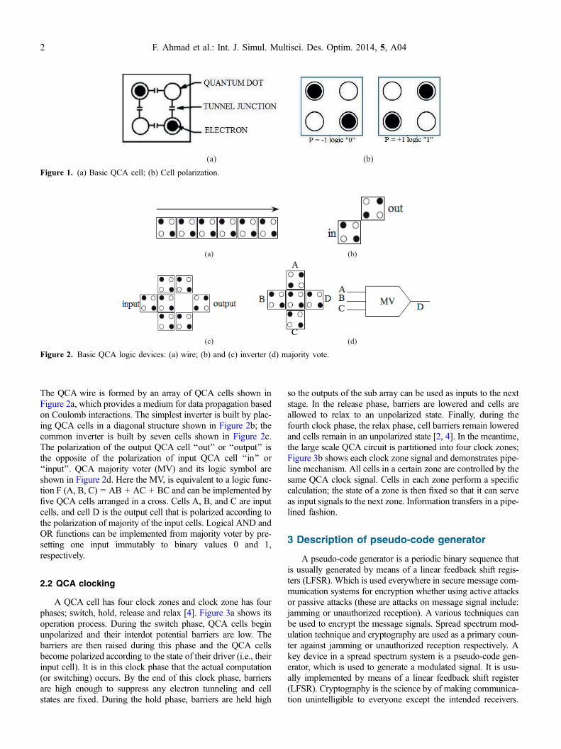
2.2 QCA clocking
A QCA cell has four clock zones and clock zone has fourphases; switch, hold, release and relax [4]. Figure 3a shows itsoperation process. During the switch phase, QCA cells beginunpolarized and their interdot potential barriers are low. Thebarriers are then raised during this phase and the QCA cellsbecome polarized according to the state of their driver (i.e., theirinput cell). It is in this clock phase that the actual computation(or switching) occurs. By the end of this clock phase, barriersare high enough to suppress any electron tunneling and cellstates are fixed. During the hold phase, barriers are held high
so the outputs of the sub array can be used as inputs to the nextstage. In the release phase, barriers are lowered and cells areallowed to relax to an unpolarized state. Finally, during thefourth clock phase, the relax phase, cell barriers remain loweredand cells remain in an unpolarized state [2, 4]. In the meantime,the large scale QCA circuit is partitioned into four clock zones;Figure 3b shows each clock zone signal and demonstrates pipe-line mechanism. All cells in a certain zone are controlled by thesame QCA clock signal. Cells in each zone perform a specificcalculation; the state of a zone is then fixed so that it can serveas input signals to the next zone. Information transfers in a pipe-lined fashion.
3 Description of pseudo-code generator
A pseudo-code generator is a periodic binary sequence thatis usually generated by means of a linear feedback shift regis-ters (LFSR). Which is used everywhere in secure message com-munication systems for encryption whether using active attacksor passive attacks (these are attacks on message signal include:jamming or unauthorized reception). A various techniques canbe used to encrypt the message signals. Spread spectrum mod-ulation technique and cryptography are used as a primary coun-ter against jamming or unauthorized reception respectively. Akey device in a spread spectrum system is a pseudo-code gen-erator, which is used to generate a modulated signal. It is usu-ally implemented by means of a linear feedback shift register(LFSR). Cryptography is the science by of making communica-tion unintelligible to everyone except the intended receivers.
(a) (b) Figure 1. (a) Basic QCA cell; (b) Cell polarization.
(a) (b)
(c) (d)
Figure 2. Basic QCA logic devices: (a) wire; (b) and (c) inverter (d) majority vote.
2 F. Ahmad et al.: Int. J. Simul. Multisci. Des. Optim. 2014, 5, A04
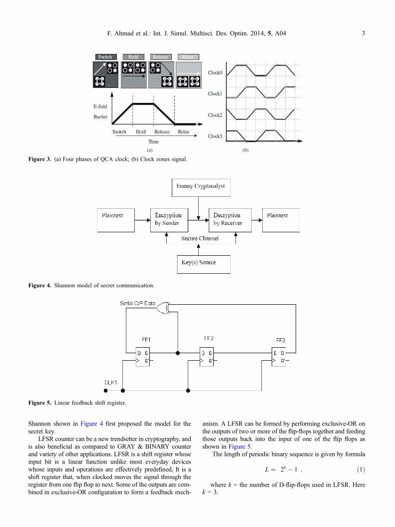
Shannon shown in Figure 4 first proposed the model for thesecret key.
LFSR counter can be a new trendsetter in cryptography, andis also beneficial as compared to GRAY & BINARY counterand variety of other applications. LFSR is a shift register whoseinput bit is a linear function unlike most everyday deviceswhose inputs and operations are effectively predefined, It is ashift register that, when clocked moves the signal through theregister from one flip flop to next. Some of the outputs are com-bined in exclusive-OR configuration to form a feedback mech-
anism. A LFSR can be formed by performing exclusive-OR onthe outputs of two or more of the flip-flops together and feedingthose outputs back into the input of one of the flip flops asshown in Figure 5.
The length of periodic binary sequence is given by formula
L ¼ 2k � 1� �
; ð1Þ
where k = the number of D-flip-flops used in LFSR. Herek = 3.
(a) (b)
Figure 3. (a) Four phases of QCA clock; (b) Clock zones signal.
Figure 4. Shannon model of secret communication.
Figure 5. Linear feedback shift register.
F. Ahmad et al.: Int. J. Simul. Multisci. Des. Optim. 2014, 5, A04 3
All the flip-flops are loaded with any bit pattern sequenceexcept (0000), which will circulate ‘‘0’’ throughout the wholeshift register because 0 + 0 = 0 by performing modulo 2-addition.
The bit pattern to be loaded can be anyone of the following001, 010, 011, etc. let us assume that initial bit pattern will be001, Period of sequence = 23 � 1 = 7.
Sequence will repeat itself seven times as shown in Table 1.
4 Results and discussions: implementationof pseudo-code generator
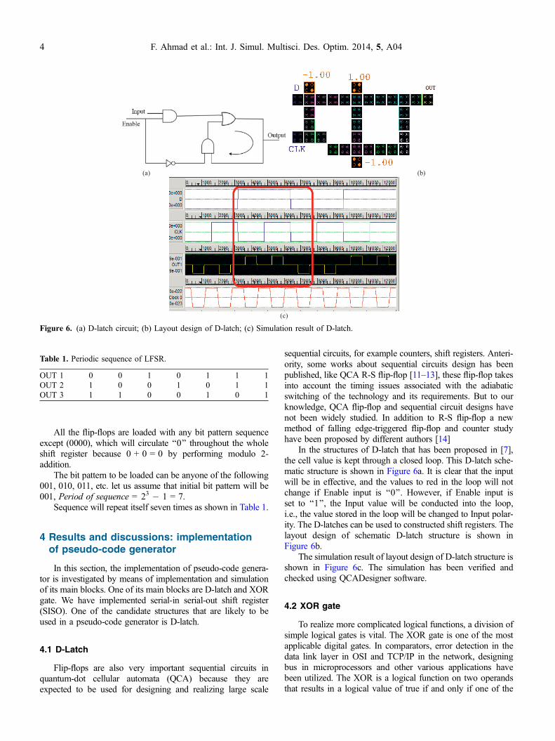
In this section, the implementation of pseudo-code genera-tor is investigated by means of implementation and simulationof its main blocks. One of its main blocks are D-latch and XORgate. We have implemented serial-in serial-out shift register(SISO). One of the candidate structures that are likely to beused in a pseudo-code generator is D-latch.
4.1 D-Latch
Flip-flops are also very important sequential circuits inquantum-dot cellular automata (QCA) because they areexpected to be used for designing and realizing large scale
sequential circuits, for example counters, shift registers. Anteri-ority, some works about sequential circuits design has beenpublished, like QCA R-S flip-flop [11–13], these flip-flop takesinto account the timing issues associated with the adiabaticswitching of the technology and its requirements. But to ourknowledge, QCA flip-flop and sequential circuit designs havenot been widely studied. In addition to R-S flip-flop a newmethod of falling edge-triggered flip-flop and counter studyhave been proposed by different authors [14]
In the structures of D-latch that has been proposed in [7],the cell value is kept through a closed loop. This D-latch sche-matic structure is shown in Figure 6a. It is clear that the inputwill be in effective, and the values to red in the loop will notchange if Enable input is ‘‘0’’. However, if Enable input isset to ‘‘1’’, the Input value will be conducted into the loop,i.e., the value stored in the loop will be changed to Input polar-ity. The D-latches can be used to constructed shift registers. Thelayout design of schematic D-latch structure is shown inFigure 6b.
The simulation result of layout design of D-latch structure isshown in Figure 6c. The simulation has been verified andchecked using QCADesigner software.
4.2 XOR gate
To realize more complicated logical functions, a division ofsimple logical gates is vital. The XOR gate is one of the mostapplicable digital gates. In comparators, error detection in thedata link layer in OSI and TCP/IP in the network, designingbus in microprocessors and other various applications havebeen utilized. The XOR is a logical function on two operandsthat results in a logical value of true if and only if one of the
(a) (b)
(c)
Figure 6. (a) D-latch circuit; (b) Layout design of D-latch; (c) Simulation result of D-latch.
Table 1. Periodic sequence of LFSR.
OUT 1 0 0 1 0 1 1 1OUT 2 1 0 0 1 0 1 1OUT 3 1 1 0 0 1 0 1
4 F. Ahmad et al.: Int. J. Simul. Multisci. Des. Optim. 2014, 5, A04

(a)
(b) Figure 7. (a) The proposed layouts of XOR gates; (b) Simulation results of proposed designs.
(a) (b)
Figure 8. (a) Schematic of SISO register; (b) Timing diagram.
F. Ahmad et al.: Int. J. Simul. Multisci. Des. Optim. 2014, 5, A04 5
operands, but not both, has a value of true. It is designed use ofmajority gates and inverters. Formula below presents the equa-tion for this gate.
XOR ¼ MVðMV A0; B; 0ð Þ; MV A; B0; 0ð Þ; 1Þ: ð2Þ
(XOR) and exclusive-OR (NOR) gates are also used indigital circuits, have been proposed by different authors [8–10]. The design has complexity of cells and either coplanarcrossovers or multiple layers to implement. In this paper therewas an attempt to design simple XOR structures. The inputs
Figure 9. Layout design of SISO register.
(a)
(b)
Figure 10. (a) Vector table simulation result; (b) Exhaustive simulation result.
6 F. Ahmad et al.: Int. J. Simul. Multisci. Des. Optim. 2014, 5, A04

of circuit are A and B and the output is XOR signal. In thisdesign, multilayer has not been used and this caused consider-able reduction in the number of cells in circuit. The circuit lay-out has been displayed in Figure 7a.
The XOR gate was considered for various inputs and theirsimulation results have been shown in Figure 7b.
The number of cells of the proposed gates and their polar-ities has been compared with previous structures [8–10]. Com-parisons between the proposed and conventional XOR gates aregiven in Table 2.
Figure 11. Layout design of pseudo-code generator.
(b)
(c) Figure 12. Exhaustive simulation result of pseudo-code.
Table 2. Comparison of conventional and proposed layouts.
Logic structures Complexityno. of cells
Area(lm2)
Latencyclockingcycles
Conventionalstructures
84 0.08 1
64 0.07 1Proposed structures 34 0.06 1
42 0.05 1/2
F. Ahmad et al.: Int. J. Simul. Multisci. Des. Optim. 2014, 5, A04 7

4.3 Serial-in/serial-out (SISO) shift register
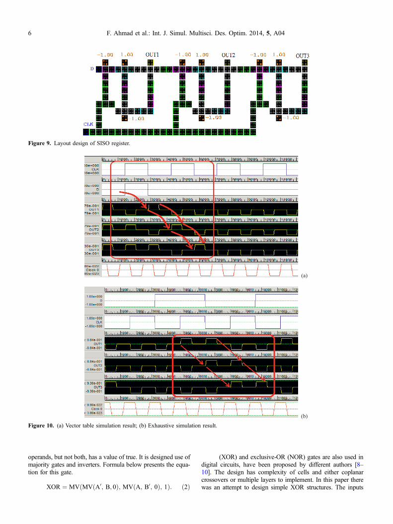
In this subsection, serial-in/serial-out (SISO) shift registerhas been proposed using QCA D-latch [7] structure. These reg-isters are a type of sequential logic circuit, mainly for storage ofdigital data. They are a group of D-flip-flops, connected in achain so that the output from one flip-flop becomes the inputof the next flip-flop. Most of the registers possess no character-istic internal sequence of states. All flip-flops are driven by acommon clock, and all are set or reset simultaneously. Theschematic structure of serial-in/serial-out (SISO) shift registersis shown in Figure 8a and its timing diagram is shown inFigure 8b respectively.
The layout design of serial-in/serial-out shift register isshown in Figure 9. A serial-in/serial-out shift register has aclock input, a data input, and a data output from the last stage.In general, the other stage outputs are not available otherwise; itwould be a serial-in, parallel-out shift register.
Both vector table setup, exhaustive verification simulationresult of serial-in/serial-out shift register is shown Figures 10aand 10b respectively. The waveforms below are applicable toeither one of the preceding two versions of the serial-in,serial-out shift register. The three pairs of arrows show that athree stage shift register temporarily stores 3-bits of data anddelays it by three clock periods from input to output.
4.4 Pseudo-code generator
Pseudo-code generator is shown in Figure 11. The dashedcircle used in Figure 11 can be used to initilize the inputputserial data bit of pseudo-code generator. Thereafter length ofsequence will repeat itself as per formula (1). To distinguishclock zones, four different colors have been employed. Thesedifferent zones are required for timing circuit.
The simulation result of exhaustive simulation result ofpseudo-code generator is shown in Figure 12.
5 Conclusion
QCA implementation of pseudo-code generator is discussedin this paper. The main blocks of this algorithm which areD-latch, XOR-gate and shift registers, have been implementedand simulated separately. It is demonstrated that the implemen-tation of cryptographic algorithms in this technology has con-siderable advantageous as compared to conventional CMOSapproach. It has shown that the QCA design of logic circuitsis challenged with unique features at logic level. In this respect,it has been proved that design of PN-Code generators offers thebest advantage of versatility and ease of implementation usingthe communication circuits. Simulations were performed usinga set of Vector table simulation and exhaustive simulation resultof QCA designer.
Acknowledgements. One of the authors is highly thankful to UGC,India for providing Dr. D.S. Kothari UGC-PDF for carrying out thiswork. We are also thankful to Prof.G.M. Bhat and Mr. Hilal A. Khanof Electronics and Instrumentation Department for help and neces-sary discussions.
References
1. Lent CS, Taugaw PD, Porod W, Berstein GH. 1993. Quantumcellular automata. Nanotechnology, 4, 49.
2. Cho H, Swartzlander EE Jr. 2009. Adder and multiplier designin quantum-dot cellular automata. IEEE Transactions onComputers, 58(6), 721–727.
3. Amlani I, Orlov AO, Toth G, Bernstein GH, Lent CS, SniderGL. 1999. Digital 7 logic gate using quantum-dot cellularautomata. Science, 284(5412), 289–291.
4. Lent CS, Tougaw PD. 1997. A device architecture forcomputing with quantum dots. Proceedings of the IEEE,85(4), 541–557.
5. Tougaw PD, Lent CS. 1996. Dynamic behavior of quantumcellular automata. Journal of Applied Physics, 80(8),4722–4735.
6. Tougaw PD, Lent CS, Porod W. 1993. Bistable saturation incoupled quantum-dot cells. Journal of Applied Physics, 74(5),3558–3565.
7. Walus K, Vetteth A, Jullien GA,Dimitrov VS. 2003. RAMdesignusing quantum-dot cellular automata. Technical Proceedings ofthe Nanotechnology Conference and Trade Show, 2, 160–163.
8. Karthigai Lakshmi S, Athisha G. 2010. Efficient design oflogical structures and functions using nanotechnology basedquantum dot cellular automata design. International Journal ofComputer Applications, 3(5), 0975–0887.
9. Tougaw PD, Lent CS. 1999. Logical devices implementationusing quantum dot cellular automata. Journal of AppliedPhysics, 75, 1818.
10. Ch VT, Polisetti S, Santhosh K. 2008. QCA based multiplexingof 16 arithmetic & logical subsystem-a paradigm for nanocomputing, 3rd Annual IEEE-International conference on Nano/Micro Engineering Molecular System, Hainan Island, China.
11. Vankamamidi V, Ottavi M, Lombardi F. 2008. Two dimensionalschemes for clocking/timing of QCA circuits. IEEE Transac-tions on Computer-Aided Design of Integrated Circuits andSystems, 27(1), 34–44.
12. Momenzadeh M, Huang J, Lombardi F. 2005. Defect charac-terization and tolerance of QCA sequential devices and circuits,IEEE International Symposium on Defect and Fault Tolerancein VLSI Systems, Monterey, California, USA. p. 199.
13. Huang J, Momenzadeh M, Lombardi F. 2007. Design ofsequential circuits by quantum-dot cellular automata. Micro-electronics Journal, 38, 525–537.
14. Yang XK, Cai L, Zhao XH, Zhang NS. 2010. Design andSimulation of Sequential Circuits in Quantum-Dot CellularAutomata: Falling Edge-Triggered Flip-Flop and Counter Study.College of Science, Air Force Engineering University: Xi’an,China.
Cite this article as: Ahmad F, Mustafa M, Wani AN & Mir AF: A novel idea of pseudo-code generator in quantum-dot cellularautomata (QCA). Int. J. Simul. Multisci. Des. Optim., 2014, 5, A04.
8 F. Ahmad et al.: Int. J. Simul. Multisci. Des. Optim. 2014, 5, A04