a microfluidic 2×2 optical switch
TRANSCRIPT

A microfluidic 2 × 2 optical switchKyle Campbell, Alex Groisman, Uriel Levy, Lin Pang, Shayan Mookherjea, Demetri Psaltis, and Yeshaiahu
Fainman
Citation: Applied Physics Letters 85, 6119 (2004); doi: 10.1063/1.1839281 View online: http://dx.doi.org/10.1063/1.1839281 View Table of Contents: http://scitation.aip.org/content/aip/journal/apl/85/25?ver=pdfcov Published by the AIP Publishing Articles you may be interested in Fabrication of stationary micro-optical shutter based on semiconductor-to-metallic phase transition of W-dopedVO 2 active layer driven by an external voltage J. Vac. Sci. Technol. A 26, 763 (2008); 10.1116/1.2870227 The electrical and mechanical properties of Au–V and Au – V 2 O 5 thin films for wear-resistant RF MEMSswitches J. Appl. Phys. 103, 083522 (2008); 10.1063/1.2902954 Observation of femtojoule optical bistability involving Fano resonances in high- Q V m silicon photonic crystalnanocavities Appl. Phys. Lett. 91, 051113 (2007); 10.1063/1.2757607 Micro-optical switch device based on semiconductor-to-metallic phase transition characteristics of W-doped V O2 smart coatings J. Vac. Sci. Technol. A 25, 971 (2007); 10.1116/1.2734150 A polarization insensitive 2 × 2 optical switch fabricated by liquid crystal–polymer composite Appl. Phys. Lett. 86, 041115 (2005); 10.1063/1.1857092
This article is copyrighted as indicated in the article. Reuse of AIP content is subject to the terms at: http://scitation.aip.org/termsconditions. Downloaded to IP: 129.174.21.5
On: Sun, 06 Jul 2014 09:31:09
A microfluidic 2 Ã2 optical switchKyle Campbell and Alex Groismana)
Department of Physics, University of California, San Diego, 9500 Gilman Drive,La Jolla, California 92093
Uriel Levy, Lin Pang, and Shayan MookherjeaDepartment of Electrical and Computer Engineering, University of California, San Diego,9500 Gilman Drive, La Jolla, California 92093
Demetri PsaltisDepartment of Electrical Engineering, California Institute of Technology, Pasadena, California 91125
Yeshaiahu FainmanDepartment of Electrical and Computer Engineering, University of California, San Diego,9500 Gilman Drive, La Jolla, California 92093
(Received 12 August 2004; accepted 19 October 2004)
A 232 microfluidic-based optical switch is proposed and demonstrated. The switch is made of anoptically clear silicon elastomer, Polydimethylsiloxane(PDMS), using soft lithography. It hasinsertion loss smaller than 1 dB and extinction ratio on the order of 20 dB. The device is switchingbetween transmission(bypass) and reflection(exchange) modes within less than 20 ms. ©2004American Institute of Physics. [DOI: 10.1063/1.1839281]
Optical switching devices play an important role in mod-ern telecommunication networks providing unique function-alities such as optical add/drop, optical cross connect, andring protection. A variety of switching devices based onelectro-optic, thermo-optic, mechanical, acousto-optic, andmagneto-optic modulation techniques have been developedduring past years.1–5 A few designs used the effect of totalinternal reflection(TIR) and had crossing regions betweencoupled waveguides filled with index matching liquids.6,7 Agas bubble with the liquid–air interface acting as a mirrorwas either driven into the crossing region by a thermo-capillary force6 or created in it using the inkjet technology.7
In this letter we demonstrate a 232 all optical switchbased on control of TIR by flowing two different mixableliquids through microscopic channels made of a transparentsilicon elastomer. With the advent of soft lithography andrapid prototyping,8 the silicon elastomer Polydimethylsilox-ane(PDMS) has become a material of choice for many mi-crofluidic R&D and lab-on-a-chip applications. The devicesmade of PDMS are inexpensive and their fabrication doesnot require high-level facilities. PDMS has quite lowYoung’s modulus that allows construction of adaptive lenseswith thin flexible membranes.9,10 The flexible elastomermembranes are also a key element in pressure-actuatedmicro-valves that can be integrated in the microfluidicdevices.11,12A specific advantage of PDMS for a fluidic op-tical switch is its low index of refraction,ne=1.41, which canbe easily matched by low viscosity, nontoxic aqueous saltsolutions.
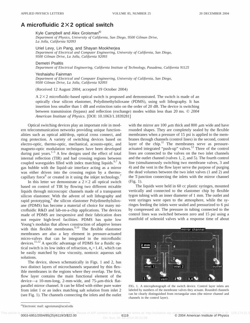
The device, shown schematically in Figs. 1 and 2, hastwo distinct layers of microchannels separated by thin flex-ible membranes in the regions where they overlap. The first,flow layer contains the main functional element of thedevice—a 10-mm-long, 2-mm-wide, and 75-mm-thick flat-parallel mirror channel. It can be filled with either pure waterfrom inlet 1 or an index matching salt solution from inlet 2(see Fig. 1). The channels connecting the inlets and the outlet
with the mirror are 100mm thick and 800mm wide and haverounded shapes. They are completely sealed by the flexiblemembranes when a pressure of 15 psi is applied to the mem-branes through channels(control lines) in the second, controllayer of the chip.11 The membranes serve as pressure-actuated integrated “push-up” valves.12 Three of the controllines are connected to the valves on the two inlet channelsand the outlet channel(valves 1, 2, and 5). The fourth controlline (simultaneously switching two membrane valves, 3 and4) and the vent in the flow layer serve the purpose of purgingthe dead volumes between the two inlet valves(1 and 2) andthe T-junction connecting the inlets with the mirror channel(Fig. 1).
The liquids were held in 60 cc plastic syringes, mountedvertically and connected to the elastomer chip by flexibletygon tubing with an inner diameter of 1 mm. The outlet andvent syringes were open to the atmosphere, while the sy-ringes feeding the inlets were sealed and pressurized to 6 psiby compressed air. The pressure in tubing connected to thecontrol lines was switched between zero and 15 psi using amanifold of solenoid valves with a response time of about
a)Electronic mail: [email protected]
FIG. 1. A microphotograph of the switch device. Control layer inlets arelabeled by numbers of the membrane valves they actuate. Rounded channelscan be clearly distinguished from rectangular ones(the mirror channel andchannels in the control layer).
APPLIED PHYSICS LETTERS VOLUME 85, NUMBER 25 20 DECEMBER 2004
0003-6951/2004/85(25)/6119/3/$22.00 © 2004 American Institute of Physics6119 This article is copyrighted as indicated in the article. Reuse of AIP content is subject to the terms at: http://scitation.aip.org/termsconditions. Downloaded to IP: 129.174.21.5
On: Sun, 06 Jul 2014 09:31:09
4 ms. The valves were driven by a homemade controller in-terfaced with a PC through a National Instruments DAQcard.
All the membrane valves were normally pressurized andclosed, and there was no flow in the channels. The opticalswitching was performed by filling the mirror channel with aliquid having a different index of refraction. If, for example,the water had to be exchanged by the salt solution, valves2–5 were opened simultaneously(by switching pressure inthe corresponding control lines to zero) to start flow frominlet 2 toward the outlet and the vent. The valves 2, 3, and 4were closed after 100 ms, a time interval corresponding to aliquid discharge of about 4 mirror channel volumess7 mld inthe flow from inlet 2 to the outlet. Closing valve 5 was de-layed by 20 ms to allow pressure relief in the mirror channel.
The condition of TIR at the interface between the PDMSelastomer with a refraction indexne<1.41 and de-ionizedwater withnw<1.33 is met at angles of incidence larger than70.6°. Therefore the microfluidic chips were made with op-tically flat, clear facets at angles of 75° to the plane of thechannels on both sides(see Fig. 2), and the incident beamswere directed normally to the facets, Fig. 2(c). The indexmatching liquid was a solution of about 35% KI and 15%NaBr (by weight) in water. Its viscosity was nearly as low asthe viscosity of waters10−3 Pa sd allowing high flow rate andfast switching at moderate driving pressures.
The device was made using the technique of soft lithog-raphy and was assembled from three layers of PDMS(seeFig. 2). Two of the layers had microchannel relief engravedon their surfaces(flow and control channels), and they werecast using two different master molds. The molds were fab-ricated by the regular near-UV contact photolithography us-ing 8000 dpi resolution masks designed to implement thedesired geometry of the molds. To make the master mold forthe flow layer, a 4 in. silicon wafer was first spin coated with75-mm-thick layer of a negative photoresist(SU8-2050 byMicroChem) and patterned through a photomask. That pro-duced flat parallel relief to cast the mirror channels. Next, thewafer was coated with about 100mm layer of a positiveresist, AZ100 XT by Clariant. It was patterned through an-other photomask(aligned with respect to the 75mm SU8layer), and baked on a 140° hot plate for 30 min after devel-opment to round the AZ 100XT relief11,12[see Fig. 2(a)]. Themold for the control channels was made by spin coatinganother 4 in. wafer with a 100-mm-thick layer of SU8-2050resist and patterning it through a third photomask.
The resin and catalyst parts of the silicon elastomer(Sylgard 184 by Dow Corning) were mixed in a proportionof 5:1 and poured onto the first mold to a depth of 5 mm. Inorder to make the flat 75° facets and assure optical quality ofthe surfaces we used trapezoidal plastic bars with silanizedcover glasses glued to their sides[see Fig. 2(a)]. The coverglasses were immersed into the liquid elastomer and the con-struct was baked for 25 min in an 80 °C oven to partiallycure the elastomer. The elastomer was then separated fromthe glasses and the wafer, cut into individual chips, and holeswere punched in the chips with a gauge 16 luer stub to makeports for the flow layer.
In parallel the second mold was spin coated with a,160-mm-thick layer of elastomer(20:1 mixture of the resinand catalyst). The elastomer was partially cured in the oven,and the chips were placed on top of it aligned with the pho-toresist relief on the mold11,12 [see Fig. 2(b)]. After 2 h ofbaking in the oven a monolith of completely cured elastomer
TABLE I. Insertion loss and extinction ratio(in dB) for transmitted and reflected beams in the two states of theswitch and for two inputs at TE and TM.
Bypass TE(dB) Exchange TE(dB) Bypass TM(dB) Exchange TM(dB)
Laser beam 1 2 1 2 1 2 1 2Insertion loss 0.78 0.84 1.1 1.1 0.71 0.67 0.83 0.78Extinction ratio 22.7 24.4 18.2 17.7 17.8 22.5 21.7 16.7
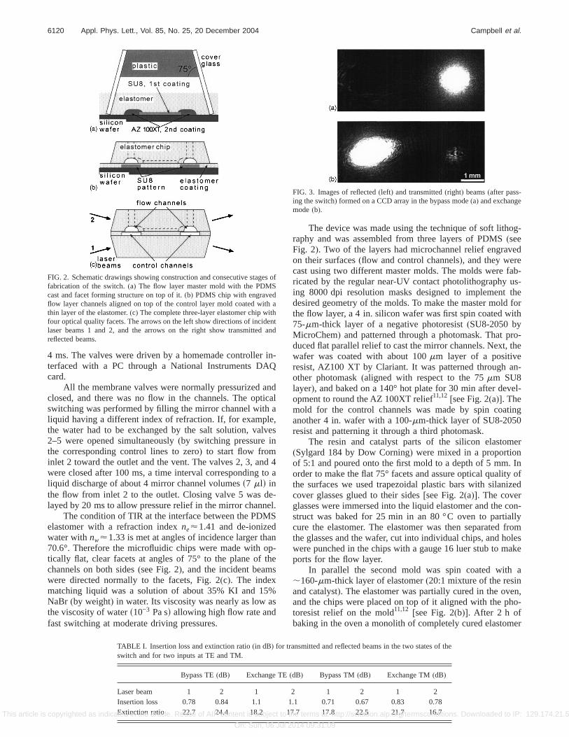
FIG. 3. Images of reflected(left) and transmitted(right) beams(after pass-ing the switch) formed on a CCD array in the bypass mode(a) and exchangemode(b).
FIG. 2. Schematic drawings showing construction and consecutive stages offabrication of the switch.(a) The flow layer master mold with the PDMScast and facet forming structure on top of it.(b) PDMS chip with engravedflow layer channels aligned on top of the control layer mold coated with athin layer of the elastomer.(c) The complete three-layer elastomer chip withfour optical quality facets. The arrows on the left show directions of incidentlaser beams 1 and 2, and the arrows on the right show transmitted andreflected beams.
6120 Appl. Phys. Lett., Vol. 85, No. 25, 20 December 2004 Campbell et al.
This article is copyrighted as indicated in the article. Reuse of AIP content is subject to the terms at: http://scitation.aip.org/termsconditions. Downloaded to IP: 129.174.21.5
On: Sun, 06 Jul 2014 09:31:09

with integrated valves was formed. The elastomer was cutinto individual chips and holes were punched in the chipswith a gauge 20 luer stub to make ports for the control layer.The control channels on the surface of the chips were sealedby ,5-mm-thick pieces of the elastomer with flat surfacesand the same trapezoidal profile with 75° facets[see Fig.2(c)], which were made using a procedure similar to thatdescribed earlier.(Both surfaces were treated with oxygenplasma for improved bonding.) The complete three-layer de-vice had a hexagonal profile with the microchannels near themidplane. It was optically clear and the interfaces betweendifferent layers were not detectable by eye.
Characterization of the device was performed using a2 mm collimated beam derived from a single mode HeNelaser sourcesl=632.8 nmd. The laser beam was directed tothe mirror channel(see Fig. 1) either from above[beam 1,Fig. 2(c)] or below[beam 2, Fig. 2(c)] normally to one of thefacets. Thus, the angle of incidence on the surface of themirror channel was 75° for both beams. The channel acted asa mirror (exchange mode) and a transparent window(bypassmode) when it was filled with water and with the indexmatching solution, respectively.
Images of the transmitted(bypass) and the reflected(ex-change) beams(captured with a Cohu CCD camera) areshown in Fig. 3. The mode of the beam in the bypass state ofthe switch is characterized by a high quality Gaussian shape[see Fig. 3(a)]. In the exchange state the mode is somewhatelliptical, which is probably due to a slight curvature of thePDMS-microchannel boundaries. The beam quality could beimproved by using a more elaborate fabrication procedureand PDMS with a higher Young’s modulus.13
Power of transmitted and reflected beams was measuredwith a Newport 818-SL power meter. A linear polarizer wasplaced in front of the device to explore its performance fortwo orthogonal states of polarization. Results of the measure-ments for beams 1 and 2 coming from below and above[seeFig. 2(c)], the two orthogonal linear polarization states andthe two switching states are summarized in Table I as valuesof insertion loss and extinction ratio in dB. The latter wasdefined as the ratio between the powers of the reflected(transmitted) and the incident beam in the bypass(exchange)mode. The TE polarization corresponds to the electric fieldorthogonal to the plane of incidence.
The cross talk of the device in the bypass state stronglydepends on exact matching of refractive indices of PDMSand the salt solution. At the incidence angle of 75° the mea-sured extinction ratio of 20 dB(see Table I) in the bypassstate for TE polarization corresponds to an index mismatch
of about 0.001. An extinction ratio of,45 dB, which is astandard requirement for modern telecommunicationswitches, should be reached by reducing the index mismatchdown to 0.0001. The extinction ratio in the exchange state ismainly limited by the small width of the mirror channels2 mmd and can be further improved by better collimation ofthe beam.
Part of the insertion loss, about 0.3 dB, is due to reflec-tions from the two PDMS–air interfaces and can be elimi-nated by AR coating the facets. The insertion loss inside thedevice is,0.4–0.8 dB, which is comparable with state ofthe art optical switching components. The polarization-dependent loss is on the order of 0.1–0.3 dB. Those numberscould be reduced by improving the index matching, qualityof the mirror channel surface, and by increasing the width ofthe mirror.
We tested dynamic performance of the device by switch-ing it periodically and measuring power of the beams withfast silicon photodetectors(Thorlabs 201/579-7227) con-nected to a digitizing Tektronix oscilloscope. A representa-tive time series is shown in Fig. 4. The transition from by-pass to exchange state occurred within about 20 ms(basedon 10%–90% criterion), while the transition from exchangeto bypass took less than 10 ms. This speed meets currentstandards for most switching applications(e.g., protectionand routing). The switching speed is mainly limited by therate of flow in the microchannels and can be further in-creased by applying higher pressures and increasing channeldepths.
The demonstrated optical switch is a free space devicewith the width of the mirrors2 mmd sufficient for even non-collimated laser beams. Since it is based on one-phase flowof two mixable liquids, its size can be varied without subtleeffects on its performance. Those are two main advantages ofthis device compared with the bubble photonic switchesimplemented in waveguides.7 In addition, the device fabrica-tion is based on the soft lithography replication process,which is expected to reduce cost per unit, making thisswitching technology appealing for low-end applications.The switch can also be integrated with other microfluidicdevices for lab-on-a-chip applications.
This research has been partially supported by DARPA,NSF, and AFOSR.
1A. Krishnamoorthy, F. Xu, J. E. Ford, and Y. Fainman, Appl. Opt.36, 997(1997).
2K. W. Cheung, D. A. Smith, J. E. Baran, and B. I. Heffner, Electron. Lett.25, 375 (1989).
3L. Y. Lin, E. L. Goldstein, and R. W. Tkach, IEEE Photonics Technol.Lett. 10, 525 (1998).
4A. Kar-Roy and C. S. Tsai, IEEE Photonics Technol. Lett.7, 731 (1992).5D. Marom and D. Mendlovic, Appl. Opt.35, 248 (1996).6M. Makishara, M. Sato, F. Shimokawa, and Y. Nishida, J. LightwaveTechnol. 17, 14 (1999).
7D. K. Donald, J. E. Fouquet, and M. A. Troll, US Patent No. 6,320,994(2001).
8Y. N. Xia and G. M. Whitesides, Annu. Rev. Mater. Sci.28, 153 (1998).9D. Y. Zhang, V. Lien, Y. Berdichevsky, J. Choi, and Y. H. Lo, Appl. Phys.Lett. 82, 3171(2003).
10N. Chronis, G. L. Liu, K. H. Jeong, and L. P. Lee, Opt. Express11, 2370(2003).
11M. A. Unger, H. P. Chou, T. Thorsen, A. Scherer, and S. R. Quake,Science288, 113 (2000).
12V. Studer, G. Hang, A. Pandolfi, M. Ortiz, W. F. Anderson, and S. R.Quake, J. Appl. Phys.95, 393 (2004).
13H. Schmid and B. Michel, Macromolecules33, 3042(2000).
FIG. 4. Power of transmitted and reflected beams as a function of timemeasured by fast photodetectors and visualized with an oscilloscope duringa series of periodic switching events.
Appl. Phys. Lett., Vol. 85, No. 25, 20 December 2004 Campbell et al. 6121
This article is copyrighted as indicated in the article. Reuse of AIP content is subject to the terms at: http://scitation.aip.org/termsconditions. Downloaded to IP: 129.174.21.5
On: Sun, 06 Jul 2014 09:31:09