a method of voltage tracking for power system …
TRANSCRIPT

A METHOD OF VOLTAGE TRACKING
FOR
POWER SYSTEM APPLICATIONS
BY
JACOBUS VISSER
Submitted in partial fulfillment of the requirement for the degree
Master of Science: Applied Sciences (Electrotechnics)
in the
Faculty of Engineering, Built Environment and Information Technology
UNIVERSITY OF PRETORIA
JULY 2010
©© UUnniivveerrssiittyy ooff PPrreettoorriiaa

Department of Electrical, Electronic and Computer Engineering
University of Pretoria
2
SUMMARY (ENGLISH)
Title: A method of voltage tracking for power system applications.
Student: Jacobus Visser
Study Leader: Dr. Raj Naidoo
Department: Department of Electric, Electronic and Computer Engineering,
University of Pretoria
Degree: M.Sc: Applied Sciences (Electrotechnics)
An algorithm that is capable of estimating the parameters of non-stationary sinusoids in
real-time lends application to various branches of engineering. Non-stationary sinusoids
are sinusoidal signals with time-varying parameters.
In this dissertation, a nonlinear filter is applied to power system applications to test its
performance. The filter has a structure which renders it fully adaptive to tracking time
variations in the parameters of the targeted sinusoid, including its phase and frequency.
Mathematical properties of the differential equations which govern the proposed filter are
presented. The performance of the proposed filter in the field of power systems is
demonstrated with the aid of computer simulations and practical experimentations.
The filter is applied to synchronous generator excitation control, voltage dip mitigation as
well as the real-time estimation of symmetrical components. The parameter settings of the
filter are tested and optimized for each of the applications.
This dissertation demonstrates the simulation and experimental results of the filter when
applied to the various power system applications.
Keywords: Non-linear filter, Parameter setting optimization, Diode bridge rectifier,
Amplitude tracking, Synchronous generator control, Voltage dips, Symmetrical
components.

Department of Electrical, Electronic and Computer Engineering
University of Pretoria
3
OPSOMMING
Titel: A method of voltage tracking for power system applications.
Student: Jacobus Visser
Studie Leier: Dr. Raj Naidoo
Departement: Department of Electric, Electronic and Computer Engineering,
University of Pretoria
Kursus: M.Sc: Toegepaste Wetenskappe (Electrotechnics)
'n Filter wat bevoeglik is met die beraming van die parameters van beweeglike sinusoïdale
in ware-tyd, kan bruikbaar aangewend word in verskeie takke van ingenieurswese.
Beweeglike sinuskrommes is sinusoïdale seine met tyd-wisselende parameters.
In hierdie verhandeling word `n nie-liniêre filter aangewend in verskeie
kragstelseltoepassings om die werksverrigting van die filter te toets. Die filter het 'n
struktuur wat dit toelaat om wisselende tydvariasies in die parameters van die
teikensinusoïdaal op te spoor, insluitende die fase en frekwensie. Wiskundige eienskappe
van die differensiaalvergelykings wat die voorgestelde filter beheer is ondersoek. Die
werksverrigting van die voorgestelde filter in die veld van kragstelsels is gedemonstreer
met die hulp van rekenaarsimulasies asook praktiese eksperimente.
Die filter is toegepas tot opgewekte, sinkrone eksitasie-beheer, spanningsverlaging
versagting, asook die ware tyd estimasie van simmetriese komponente. Die parameter
verstellings van die filter is getoets en geoptimeer vir elk van die toepassings.
Hierdie verhandeling demonstreer die simulering en eksperimentele resultate van die filter
wat aangewend is vir verskeie kragstelseltoepassings.
Kernwoorde: Nie-liniêre filter, Parameter verstelling optimering, Diodebrug gelykrigter,
Amplituderaming, Synkrone-generator-beheer, Spanningverlagings, Simmetriese
komponente.

Department of Electrical, Electronic and Computer Engineering
University of Pretoria
4
LIST OF ABBREVIATIONS
This list contains the abbreviations and acronyms used in this document.
AC Alternating Current
AVR Automatic Voltage Regulation
CBEMA Computer Business Equipment Manufacturers Association
CPU Central Processing Unit
CSV Comma Delimited Excel File
DBR Diode Bridge Rectifier
DC Direct Current
DFT Discrete Fourier Transform
EMF Electromagnetic Force
HT Hilbert Transform
HTS High Temperature Superconductors
Hz Hertz
IEEE Institute of Electrical and Electronic Engineers
L Inductance
LAV Least Absolute Value
LFC Load Frequency Controlled
LMS Least Mean Squares
MVA Mega Voltage-Ampere
PC Personal Computer
PLL Phase Locked Loop
RMS Root Mean Squares
SCR Silicon Controlled Rectifier
ST Static
TEO Teager Energy Operator
VAR Voltage-Ampere Reactive

Department of Electrical, Electronic and Computer Engineering
University of Pretoria
5
TABLE OF CONTENTS
CHAPTER 1 ..........................................................................................................................7
INTRODUCTION ................................................................................................................7
1.1 REVIEW OF CONVENTIONAL METHODS ........................................................7
1.2 OBJECTIVE OF THE DISSERTATION ................................................................9
1.3 OUTLINE OF THE DISSERTATION ....................................................................9
1.4 CONTRIBUTION OF THIS DISSERTATION ..................................................... 10
CHAPTER 2 ........................................................................................................................ 11
MATHEMATICAL MODEL AND PARAMETER OPTIMIZATION ........................... 11
2.1 INTRODUCTION ................................................................................................ 11
2.2 FORMULATION OF THE ALGORITHM ........................................................... 12
2.3 IMPLEMENTATION OF THE PROPOSED ALGORITHM ................................ 14
2.4 PARAMETER OPTIMIZATION FOR AMPLITUDE TRACKING ..................... 16
2.5 PARAMETER OPTIMIZATION FOR PHASE AND FREQUENCY
TRACKING ......................................................................................................... 20
2.5.1 Parameter Optimization for Phase Changes ........................................................... 20
2.5.2 Parameter Optimization for Frequency Changes .................................................... 24
2.6 CONCLUDING REMARKS ................................................................................ 26
CHAPTER 3 ........................................................................................................................ 27
EXCITATION CONTROL ON A SYNCHRONOUS GENERATOR ............................. 27
3.1 INTRODUCTION ................................................................................................ 27
3.2 BASIC SYNCHRONOUS MACHINE AND EXCITATION CONTROL
THEORY .............................................................................................................. 29
3.2.1 The Synchronous Machine .................................................................................... 29
3.2.2 Basic Control of a Synchronous Machine .............................................................. 30
3.2.3 The Excitation System .......................................................................................... 31
3.2.4 The Static Excitation System ................................................................................. 32
3.3 BASIC THEORY OF THE DIODE BRIDGE RECTIFIER ................................... 33
3.3.1 Operation of the Diode Bridge Rectifier ................................................................ 33
3.3.2 Calculation of the DC Ripple Voltage for Constant Loading ................................. 36
3.4 DIODE BRIDGE RECTIFIER MODEL ............................................................... 37
3.5 PERFORMANCE OF BOTH METHODS FOR A CHANGE IN THE
VOLTAGE MAGNITUDE ................................................................................... 40
3.7 THE CLOSED-LOOP SYSTEMS ........................................................................ 46
3.8 GENERATOR RESPONSE USING BOTH METHODS AS INPUT TO THE
AVR ..................................................................................................................... 51
3.8.1 Introduction .......................................................................................................... 51
3.8.2 Algorithm Model Simulation Tests ....................................................................... 52
3.8.3 Diode Bridge Rectifier Model ............................................................................... 52
3.8.3 Performance and Results ....................................................................................... 52
3.9 SUMMARY OF RESULTS .................................................................................. 59
3.10 CONCLUDING REMARKS ................................................................................ 59
CHAPTER 4 ........................................................................................................................ 61
APPLICATION OF THE ALGORITHM TO VOLTAGE DIP MITIGATION ............. 61
4.1 INTRODUCTION ................................................................................................ 61
4.2 SYNCHRONOUS CONDENSER CONTROL ..................................................... 63
4.2.1 Basic Synchronous Condenser Theory .................................................................. 63

Department of Electrical, Electronic and Computer Engineering
University of Pretoria
6
4.2.2 Closed Loop Voltage Mitigation Studies ............................................................... 64
4.2.3. Simulations for Changes in Loading Conditions .................................................... 67
4.2.4 Voltage Dip Mitigation under Fault Conditions on the Network ............................ 68
4.2.4.1 400kV Three Phase to Ground Fault Simulations .................................................. 68
4.2.4.2 132kV Three-Phase to Ground Fault Simulations .................................................. 69
4.2.4.3 11kV Three-Phase to Ground Fault Simulations .................................................... 70
4.2.5 Summary of Results .............................................................................................. 71
4.3 MITIGATING DECAYING DC BUS VOLTAGES ............................................. 72
4.3.1 Introduction .......................................................................................................... 72
4.3.2 Experimental Setup ............................................................................................... 73
4.2.4 Summary of Results .............................................................................................. 79
4.4. CONCLUDING REMARKS ................................................................................ 80
CHAPTER 5 ........................................................................................................................ 82
APPLICATION OF THE PROPOSED ALGORITHM FOR REAL-TIME
SYMMETRICAL COMPONENT ESTIMATION ........................................................... 82
5.1 INTRODUCTION ................................................................................................ 82
5.2 PERFORMANCE ................................................................................................. 84
5.2.1 Case 1: Effects of a Change in Amplitude ............................................................. 85
5.2.2 Case 2: Effects of a Change in Phase ..................................................................... 88
5.2.3 Case 3: Influence of Harmonics ............................................................................ 91
5.3 APPLICATION TO FIELD DATA ....................................................................... 94
5.3.1 Case 1: 400kV Transmission Line Single Phase Fault ........................................... 94
5.3.2 Case 2: 275kV Transmission Line Single Phase Fault ........................................... 97
5.4 SUMMARY OF RESULTS .................................................................................. 99
5.5 CONCLUDING REMARKS .............................................................................. 100
CHAPTER 6 ...................................................................................................................... 101
CONCLUSION ................................................................................................................. 101
6.1 INTRODUCTION .............................................................................................. 101
6.2 SUMMARY OF RESULTS ................................................................................ 101
6.2.1 Control of an Automatic Voltage Regulator on a Synchronous Generator ............ 101
6.2.2 Voltage Dip Mitigation ....................................................................................... 102
6.2.3 Real time symmetrical component estimation ..................................................... 102
6.3 FUTURE WORK ................................................................................................ 103
REFERENCES ................................................................................................................. 104
LIST OF FIGURES .......................................................................................................... 107
LIST OF TABLES ............................................................................................................ 109

Department of Electrical, Electronic and Computer Engineering
University of Pretoria
7
CHAPTER 1
INTRODUCTION
1.1 REVIEW OF CONVENTIONAL METHODS
Non-stationary sinusoids are sinusoidal signals with time-varying parameters. An
algorithm that is capable of estimating the parameters of non-stationary sinusoids in real-
time lends application to various branches of engineering. The algorithm has been applied
to the problem of elimination of power line noise potentially present on electrocardiogram
and telephone cables, the estimation of low-level biomedical signals polluted by noise and
the refinement and analysis of ultrasonic waves used in non-destructive testing of
materials.
Numerous techniques have been developed for the extraction of a single sinusoidal signal
out of a given multi-component input signal [1]. The fast and accurate estimation of
magnitude, phase and frequency of a sinusoidal signal has vast importance in the control,
monitoring and analysis of a power system.
Fourier-based techniques include the Short-time Fourier Transform, the Fast Fourier
Transform and the Discrete Fourier Transform (DFT). The main disadvantage of the
Fourier-based techniques is that measurement errors are incurred when the frequency
deviates from the nominal frequency. The Fourier-based techniques are vulnerable to noise
and require long measurement windows when small frequency deviations from nominal
value occur. The Fourier methods are of an approximating nature and presuppose only
small variations in the characteristics of the sinusoidal signal under study [1-3].
The Least Absolute Value (LAV) technique is appropriate for non-stationary signals. It has
the major drawback: it assumes the frequency parameter in advance. The LAV also has a
slow convergence rate, taking at least three cycles to settle to the correct value. This is
because of a time delay. Consequently the LAV technique is not effective for online
tracking [4, 5].

Chapter 1 Introduction
Department of Electrical, Electronic and Computer Engineering
University of Pretoria
8
The Kalman and Extended Kalman Filter suffer from complexity of structure and are
sensitive to the setting of parameters and initial conditions. Furthermore, it has a relatively
long transient response if used recursively [6]. It also has high computational requirements
because it evaluates the transcendental functions in real-time [1, 4].
Root Mean Squares (RMS) and Least Mean Squares (LMS) methods are supplemented
with forgetting and adaptation factors. They can each provide dynamic estimates of the
voltage phasor. The LMS is based on the minimization of the mean square error between
the measured values for the amplitudes and phase angles. For a nonlinear power system
model, this technique results in a reasonable parameter estimation. The RMS and LMS
methods disclose a satisfactory and similar performance. Extensive experiments on actual
data clearly demonstrates that in order to improve accuracy, pre-filtering of the raw data is
needed in order to eliminate the unavoidable effects of harmonics and offsets [6-7].
The Wavelet Transform is a powerful tool that is used to analyze sinusoidal signals. It
involves computational complexity and batch processing and it is difficult to choose the
correct wavelet. Wavelet Transform is only suitable for offline diagnosis and analysis [4].
The nonlinear Teager Energy Operator (TEO) and the linear Hilbert Transform (HT) are
novel tools for assessment and tracking as they are fast, accurate and easy to implement for
voltage tracking. TEO has a low computational burden, but in the presence of harmonics
and high frequency components a filtering operation to the input signal is mandatory to
avoid instability of the TEO operation and to smooth over the output from the HT
algorithm. HT, when used with a long filter length, provides a minimum error in tracking
both voltage and frequency. However, HT has the highest computational cost and large
time delay [4-5].
Phase-locked Loops (PLL) aims to extract a specified component of the input signal and to
track its phase variations over time. It is a fundamental concept that is used and it has the
ability to generate a sinusoidal signal, the phase of which coherently follows that of the
main component of the input signals. PLL’s have a limited frequency lock-in range and
provides only phase/frequency-adjusted sinusoidal signals. Extraction of non-stationary
sinusoids implies the adjustment of the synthesized sinusoidal signal and is not common to

Chapter 1 Introduction
Department of Electrical, Electronic and Computer Engineering
University of Pretoria
9
PLLs [1]. PLLs can reduce the measurement time, but it does not have very good
resolution or dynamic properties.
1.2 OBJECTIVE OF THE DISSERTATION
A recently developed algorithm by Ziarani [1] can be used to extract and estimate the
amplitude, phase and frequency of a non-stationery signal. The algorithm has a nonlinear
structure and is a generalization of two previously developed nonlinear adaptive
algorithms. Its successful application has been demonstrated for a number of applications
and it has shown its superiority over conventional Fourier analysis and linear adaptive
methods for sinusoidal tracking. The algorithm used in this dissertation exhibits a high
degree of immunity with regard to both external noise and internal parameter settings,
while offering structural simplicity that is crucial for real-time applications [8].
The objective of this dissertation is the application of this algorithm to selected
applications in power systems. In this dissertation the method is applied to track the
voltage amplitude, phase and frequency. Optimization of parameters and performance
issues are investigated.
1.3 OUTLINE OF THE DISSERTATION
The scope of this dissertation covers the application of the signal processing algorithm to
various power system applications. The organization of the dissertation is divided into two
parts.
Part I of the dissertation presents the mathematical properties and digital implementation of
the algorithm. Chapter 2 outlines the mathematical model and simulation for parameter
optimization for a desired performance. This is compared against common methods of
voltage amplitude tracking. Chapter 3 outlines the application of the algorithm to voltage
amplitude tracking for an automatic voltage regulator (AVR).
Part II of the dissertation presents examples of the application of the algorithm to problems
in power systems. This includes voltage dip mitigation and symmetrical component
estimation. Chapter 4 presents new methods of voltage dip mitigation with the application
of the algorithm for voltage tracking for AVR of synchronous condensers as well voltage

Chapter 1 Introduction
Department of Electrical, Electronic and Computer Engineering
University of Pretoria
10
dip mitigation on DC bus voltages through fast tracking of the input waveform for
switching purposes. Chapter 5 presents the application of the algorithm for rapid estimation
of symmetrical components in three-phase power systems. The algorithm is applied to
tracking voltage amplitude, phase and frequency in real time.
Finally, concluding remarks are presented including an outline of recommended future
research directions.
The results are documented and presented both graphically and numerically. All
simulations were done using Matlab SimulinkTM
.
1.4 CONTRIBUTION OF THIS DISSERTATION
The research identifies applications in the power system field and applies a non-linear filter
to these applications. The research includes results showing comparisons and
improvements to conventional methods in some cases. The contribution to this field of
study is the optimization of the non-linear filter to track voltage amplitude, phase and
frequency of a non-stationary sinusoid in the power system field. The non-linear filter was
applied to AVR for a synchronous generator and compared to a conventional method of
AVR for a synchronous generator. The non-linear filter is also applied to voltage dip
mitigation through the excitation control of a synchronous condenser, as well as the control
and switching of a static storage device during the occurrence of voltage dips. Finally the
non-linear filter is applied to real time symmetrical component estimation and compared to
the conventional DFT.

Department of Electrical, Electronic and Computer Engineering
University of Pretoria
11
CHAPTER 2
MATHEMATICAL MODEL AND PARAMETER OPTIMIZATION
2.1 INTRODUCTION
The Ziarani/Konrad algorithm has been developed to extract and estimate the amplitude,
phase and frequency of a non-stationary signal. It has a nonlinear structure and is a
generalization of two previously developed nonlinear adaptive algorithms. The successful
application in a number of applications has shown its superiority over conventional Fourier
analysis and linear adaptive methods for sinusoidal tracking. It exhibits a high degree of
immunity with regard to both external noise and internal parameter settings while offering
structural simplicity that is crucial for real-time applications.
The signal processing algorithm that is described is very simple in structure consisting of a
few arithmetic and trigonometric operations. It is easily implemented in software, or in a
schematic design environment. The derivation of the algorithm is outlined in the following
section. The derivation is parallel to the way that the Fourier analysis was developed. Since
the approximation is no longer a linear combination of basis vectors, the estimation cannot
be obtained in a closed form such as an inner product - a direct method of minimization
has to be employed. To this end, the gradient descent method is employed to provide a
means of estimating parameters [1, 9].

Chapter 2 Mathematical Model and Parameter Optimization
Department of Electrical, Electronic and Computer Engineering
University of Pretoria
12
2.2 FORMULATION OF THE ALGORITHM
Let v(t) represent a voltage signal in which n(t) denotes the superimposed disturbance or
noise. In a typical operation i.e. a power system, v(t) has a general form of:
∑∞
=
++=0
)()sin()(i
i tntVtv φω (2.1)
where V, ω and φ are functions of time. In a power system this function is usually
continuous and almost periodic. The sinusoidal component of this function is:
)sin()( ss tVts δω += (2.2)
where Vs is the amplitude, ω the frequency and δs the phase angle. These parameters will
vary with time depending on the load on the power system, as well as with the occurrence
of faults in the power system.
The objective of the algorithm is to extract a specified component of v(t). Let M be a
manifold containing all sinusoidal signals defined as:
))()(sin()( ttttVM δω += (2.3)
where:
],[)(],,[)(],,[)( maxminmaxminmaxmin δδδωωω ∈∈∈ ttVVtV (2.4)
Thus:
TtttVt )](),(),([)( δω=ℑ (2.5)
is the vector of the parameters which belongs to the parameter space:
TV ],,[ δωϑ = (2.6)
with T denoting the transposition matrix. The output is defined as the desired sinusoidal
component:
( ))()(sin)())(,( ttttVtts δω +=ℑ (2.7)
In order to extract a certain sinusoidal component of v(t), the solution has to be an
orthogonal projection of v(t) onto the manifold M, or alternatively it has to be an optimum
φ that minimizes the distance function d between y(t, θ(t)) and v(t) i.e.:
)]()),(,([minarg)(
tvttsdt
opt ℑ=ℑ∈ℑ ϑ
(2.8)
without being concerned about the mathematical correctness of the definition of least
squared error, which strictly speaking has to continue onto the set of real numbers.

Chapter 2 Mathematical Model and Parameter Optimization
Department of Electrical, Electronic and Computer Engineering
University of Pretoria
13
The instantaneous distance function d is used:
222 )()](,()([))(,( tettstvttd ∆ℑ−=ℑ (2.9)
The cost function is defined as:
( ))(,)),(( 2 ttdttJ ℑ∆ℑ (2.10)
Although the cost function is not quadratic, the parameter vector ℑ is estimated using the
quadratic decent method:
( ))(
])(,[)(
t
ttJ
dt
td
∂ℑ
ℑ∂=
ℑµ (2.11)
The estimated parameter vector is thus denoted by:
TtttVt )](),(),([)(
^^^^
δω=ℑ (2.12)
The complete mathematical proof is presented in [1]. The governing set of equations for
the algorithm is:
φsin1
.
ekV = (2.13)
φω cos2
.
eVk= (2.14)
ωφφ += cos3
.
eAk
(2.15)
φsin)( Vts = (2.16)
)()()( tstvte −= (2.17)
where v(t) and s(t) are the respective input and output signals of the core algorithm. The
dot represents the differentiation with respect to time and the error signal e(t) is v(t) – s(t).
The state variables V, f and ω directly provide estimates of the amplitude, phase and
frequency of v(t). Parameters k1, k2, and k3 are positive numbers that determine the
behavior of the algorithm in terms of convergence speed and accuracy. Parameter k1
controls the speed of the transient response of the algorithm with respect to variations in
the amplitude of the interfering signal. Parameters k2, and k3 control the speed of the
transient response of the algorithm with respect to variations in the frequency of the
interfering signal [9].

Chapter 2 Mathematical Model and Parameter Optimization
Department of Electrical, Electronic and Computer Engineering
University of Pretoria
14
2.3 IMPLEMENTATION OF THE PROPOSED ALGORITHM
The dynamics of the proposed algorithm present a notch filter in the sense that it extracts
one specific sinusoidal component and rejects all other components, including noise.
It is adaptive in the sense that the notch filter accommodates variations of the
characteristics of the desired output over time. The center frequency of such an adaptive
filter is specified by the initial condition frequency ω. It is the form of simple blocks
suitable for schematic software development tools.
Implementation of the proposed algorithm entails the discretization of the differential
equations describing the algorithm. The discretized form of the governing equations of the
proposed algorithm can be written as:
][sin][2][]1[ 1 nnekTnVnV S φ+=+ (2.18)
][cos][][2][]1[ 2 nnVnekTnn S φωω +=+ (2.19)
][cos][][2][][]1[ 32 nnVnekkTnTnn SS φϖφφ ++=+ (2.20)
][sin][][ nnVns φ= (2.21)
][][][ nsnvne −= (2.22)
The first order approximation for the derivative is assumed, Ts is the sampling time and n is
the time step index.
The algorithm can also be implemented as a Simulink model. Figure 2.1 shows an example
of the implementation of the algorithm within Simulink. The function of each block within
the Simulink model is self-evident. The ∫ block is an integrator generating quantity x by
inputting its derivative (dx/dt). The initial conditions are defined within such integrators.
The role of the upper branch of Figure 2.1 can be described as the amplitude estimation
process and the role of the lower branch as the phase estimation process. The two branches
are not self-sufficient and are somewhat interdependent [1].

Chapter 2 Mathematical Model and Parameter Optimization
Department of Electrical, Electronic and Computer Engineering
University of Pretoria
15
Figure 2.1: Implementation of the algorithm as a Simulink model [1].
The values of the k parameters determine the convergence speed of the algorithm. It is
shown in [1] that the values of the k parameters have to be chosen such that the two
conditions of 01 20 fk << and
2
0
2
20
<<
V
fk are roughly satisfied. Quantity f0 is the
frequency of the sinusoidal signal of interest and V is the amplitude. The choice of k3 is
independent of k2. The proposed algorithm is found to be robust not only with regards to its
internal structure, but most importantly with regards to the adjustment of its k parameters.
Numerical experiments show that the performance of the proposed algorithm is almost
unaffected by parameter variations as large as 50%. It is also shown that the proposed
algorithm is robust with regards to its external conditions [9].
In terms of the engineering performance of the system, this indicates that the output of the
system will approach a sinusoidal component of the input signal v(t). Moreover, time
variations of the parameters in v(t) are tolerated by the system. One of the issues that needs
to be considered when using the proposed algorithm is the setting of its parameters k1, k2
and k3. The value of the parameters k1, k2 and k3 determine the convergence speed versus
error compromise. The values of the k parameters were changed to better suit the
application that is presented. This was done by a trial-and-error basis as there is no
specification to determine the k parameters but only guidelines on the ranges for certain
functionalities and applications [1].
Chapter 2 Mathematical Model and Parameter Optimization
Department of Electrical, Electronic and Computer Engineering
University of Pretoria
16
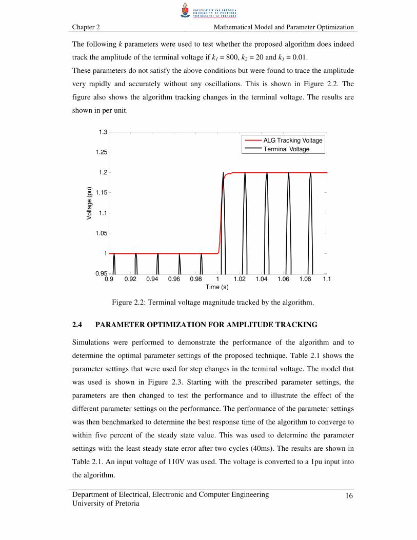
The following k parameters were used to test whether the proposed algorithm does indeed
track the amplitude of the terminal voltage if k1 = 800, k2 = 20 and k3 = 0.01.
These parameters do not satisfy the above conditions but were found to trace the amplitude
very rapidly and accurately without any oscillations. This is shown in Figure 2.2. The
figure also shows the algorithm tracking changes in the terminal voltage. The results are
shown in per unit.
0.9 0.92 0.94 0.96 0.98 1 1.02 1.04 1.06 1.08 1.10.95
1
1.05
1.1
1.15
1.2
1.25
1.3
Time (s)
Volta
ge (
pu)
ALG Tracking Voltage
Terminal Voltage
Figure 2.2: Terminal voltage magnitude tracked by the algorithm.
2.4 PARAMETER OPTIMIZATION FOR AMPLITUDE TRACKING
Simulations were performed to demonstrate the performance of the algorithm and to
determine the optimal parameter settings of the proposed technique. Table 2.1 shows the
parameter settings that were used for step changes in the terminal voltage. The model that
was used is shown in Figure 2.3. Starting with the prescribed parameter settings, the
parameters are then changed to test the performance and to illustrate the effect of the
different parameter settings on the performance. The performance of the parameter settings
was then benchmarked to determine the best response time of the algorithm to converge to
within five percent of the steady state value. This was used to determine the parameter
settings with the least steady state error after two cycles (40ms). The results are shown in
Table 2.1. An input voltage of 110V was used. The voltage is converted to a 1pu input into
the algorithm.

Chapter 2 Mathematical Model and Parameter Optimization
Department of Electrical, Electronic and Computer Engineering
University of Pretoria
17
+N
SCOPE
TEST WAVE
GENERATOR INPUT
AMPLITUDE
PHASE
FREQUENCY
Figure 2.3: Simulink model used for the testing of the algorithm’s parameter settings.
Table 2.1: The proposed algorithm’s parameter settings.
TEST
CONDUCTED
ALGORITHM
PARAMETER SETTINGS
RESPONSE
TIME (ms)
STEADY STATE
ERROR (%)
k1 k2 k3 STEP
UP
STEP
DOWN
STEP
UP
STEP
DOWN
1 100 10000 0.02 57.4 56.9 12.95 12.5
2 1000 10000 0.02 12.8 22.1 1.75 12.5
3 800 10000 0.02 12.8 22.1 1.55 1.3
4 800 100000 0.02 25 41.4 2.25 5.2
5 800 5000 0.02 21.4 31.2 0.45 3.15
6 800 20 0.02 6.3 6.3 0.05 0.15
7 800 20 0.2 6.2 6.3 0.3 0.5
8 800 20 0.1 6.3 6.3 0.15 0.35
9 800 20 0.01 6.3 6.3 0.05 0.15
Tests 1 to 3 dealt with the change in the k1 parameter with the other two parameters kept
constant. The results for Test 1 to 3 can be seen in Figure 2.4. For each test conducted a
resultant waveform is shown. The results show how the proposed algorithm tracks the step-
up (swell) and the step-down (dip) change. The response time and accuracy is
unsatisfactory. Tests 2 and 3 show the best response in tracking the step-up change.
Oscillations and overshooting is experienced in tracking the change of the terminal
voltage. The result shows that as the k1 parameter is increased, the response time of the
algorithm tracking ability decreases. However, inaccuracy due to oscillations and
overshooting of up to 5% are experienced. The overshooting and oscillation result in time
delays of the algorithm to reach the new nominal value.
Chapter 2 Mathematical Model and Parameter Optimization
Department of Electrical, Electronic and Computer Engineering
University of Pretoria
18
0.8 1 1.2 1.4 1.6 1.8 2 2.20.9
0.95
1
1.05
1.1
1.15
1.2
1.25
1.3
Time (s)
Volta
ge (
pu)
Test1
Test2
Test3
Figure 2.4: Algorithm amplitude tracking results for tests 1 to 3.
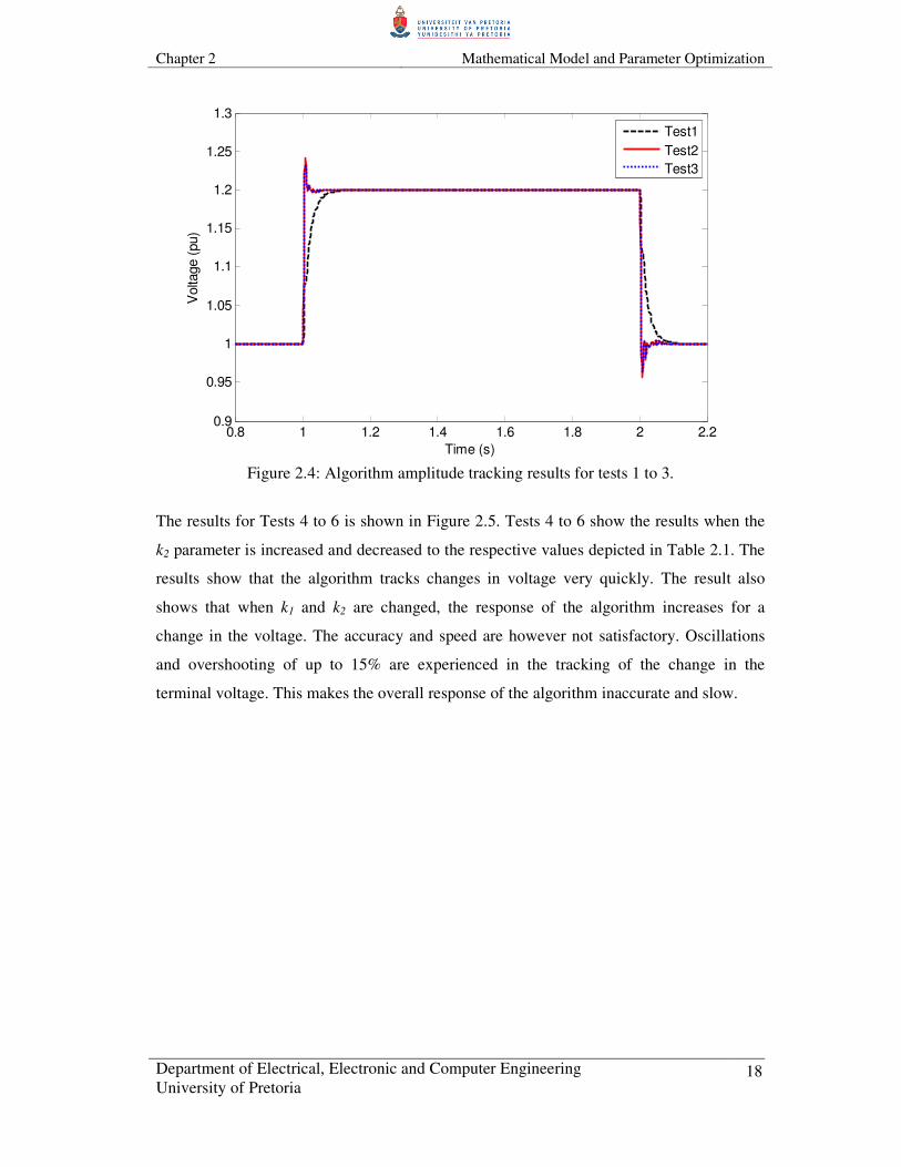
The results for Tests 4 to 6 is shown in Figure 2.5. Tests 4 to 6 show the results when the
k2 parameter is increased and decreased to the respective values depicted in Table 2.1. The
results show that the algorithm tracks changes in voltage very quickly. The result also
shows that when k1 and k2 are changed, the response of the algorithm increases for a
change in the voltage. The accuracy and speed are however not satisfactory. Oscillations
and overshooting of up to 15% are experienced in the tracking of the change in the
terminal voltage. This makes the overall response of the algorithm inaccurate and slow.

Chapter 2 Mathematical Model and Parameter Optimization
Department of Electrical, Electronic and Computer Engineering
University of Pretoria
19
0.8 1 1.2 1.4 1.6 1.8 2 2.20.8
0.85
0.9
0.95
1
1.05
1.1
1.15
1.2
1.25
1.3
Time (s)
Volta
ge (
pu)
Test4
Test5
Test6
Figure 2.5: Algorithm amplitude tracking results for tests 4 to 6.
Tests 7 to 9 deal with the change in the k3 parameter with the other two parameters kept
constant. The k3 parameter is increased and decreased to the respective values shown in
Table 2.1. The results for Test 7 to 9 is shown in Figure 2.6. Figure 2.6 shows how the
algorithm tracks the changes in the voltage amplitude. The result shows how the algorithm
tracks the settings used in Test 7. A stable and a satisfactory output is achieved. The
decrease in the k3 parameter had a major influence on the response of the algorithm. This
caused a stable result in the value of the terminal voltage. The result for Test 9 shows that
the algorithm can track the changes in the voltage amplitude very quickly and accurately
with minor overshooting. The settings used for Test 9 vary with Tests 7 and 8. The results
were found to be very close to each other for a step change in the amplitude.

Chapter 2 Mathematical Model and Parameter Optimization
Department of Electrical, Electronic and Computer Engineering
University of Pretoria
20
0.8 1 1.2 1.4 1.6 1.8 2 2.20.9
0.95
1
1.05
1.1
1.15
1.2
1.25
1.3
Time (s)
Volta
ge (
pu)
Test7
Test8
Test9
Figure 2.6: Algorithm amplitude tracking results for tests 7 to 9.
2.5 PARAMETER OPTIMIZATION FOR PHASE AND FREQUENCY
TRACKING
Simulations were performed to determine the optimal parameter settings of the proposed
technique for phase and frequency changes. The same procedure was used as for the
parameter optimization in section 2.3. Starting with the prescribed parameter settings, the
parameters are then changed to test the performance and to illustrate the effect of the
different parameter settings on the performance. The performance of the parameter settings
was then benchmarked to determine the best response time for the algorithm to converge to
within five percent of the steady state value. This was used to determine the parameter
settings with the least steady state error after two cycles (40ms).
2.5.1 Parameter Optimization for Phase Changes
Simulations were performed to determine the optimum parameters for tracking the phase
angle of an input signal under normal and changing conditions. A phase angle step change
of 60° in a forward (anti-clockwise) and reverse (clockwise) direction were performed. The
phase angle was first shifted forward by 60° and then in reverse by 60°. Figure 2.7 shows
the 60° forward and reverse phase shift vectors. During the phase changes the voltage
amplitude is kept constant.

Chapter 2 Mathematical Model and Parameter Optimization
Department of Electrical, Electronic and Computer Engineering
University of Pretoria
21
Figure 2.7: Forward and reverse phase shifts.
Figure 2.8 and 2.9 show the algorithm tracking the phase angle change of 60° in both
directions with the normal parameter settings of k1 = 100, k2 = 10000 and k3 = 0.02. The
step changes in the phase angle were done at one second as shown in Figure 2.8 and at 1.2
seconds as shown in Figure 2.9. The results show that the algorithm can track the phase
accurately and will track the change to converge in three cycles.
Figures 2.10 and 2.11 show the algorithm tracking the phase angle change of 60° in both
directions. The optimized parameter settings of k1 = 80, k2 = 10000 and k3 = 1.8 was used.
The step changes in the phase angle were done at one second as shown in Figure 2.10 and
at 1.2 seconds as shown in Figure 2.11. The results show that the algorithm can track the
phase accurately and will converge within half a cycle. Using the optimized parameter
settings a two cycle improvement in the speed of the response is achieved.

Chapter 2 Mathematical Model and Parameter Optimization
Department of Electrical, Electronic and Computer Engineering
University of Pretoria
22
0.99 1 1.01 1.02 1.03 1.04 1.05 1.06 1.07 1.08 1.09
-1
-0.8
-0.6
-0.4
-0.2
0
0.2
0.4
0.6
0.8
1
Time (s)
Volta
ge (
pu)
ALG Tracked Voltage
Input Voltage
Figure 2.8: Algorithm phase tracking for 60° forward step change with normal parameters.
1.19 1.2 1.21 1.22 1.23 1.24 1.25 1.26 1.27 1.28 1.29
-1
-0.8
-0.6
-0.4
-0.2
0
0.2
0.4
0.6
0.8
1
Time (s)
Volta
ge (
pu)
ALG Tracked Voltage
Input Voltage
Figure 2.9: Phase tracking for 60° backward step change with normal parameters.

Chapter 2 Mathematical Model and Parameter Optimization
Department of Electrical, Electronic and Computer Engineering
University of Pretoria
23
0.98 0.985 0.99 0.995 1 1.005 1.01 1.015 1.02 1.025 1.03
-1
-0.8
-0.6
-0.4
-0.2
0
0.2
0.4
0.6
0.8
1
Time (s)
Volta
ge (
pu)
ALG Tracked Voltage
Input Voltage
Figure 2.10: Phase tracking for 60° forward step change with optimized parameters.
1.19 1.195 1.2 1.205 1.21 1.215 1.22 1.225 1.23 1.235 1.24
-1
-0.8
-0.6
-0.4
-0.2
0
0.2
0.4
0.6
0.8
1
Time (s)
Volta
ge (
pu)
ALG Tracked Voltage
Input Voltage
Figure 2.11: Phase tracking for 60° backward step change with optimized parameters.

Chapter 2 Mathematical Model and Parameter Optimization
Department of Electrical, Electronic and Computer Engineering
University of Pretoria
24
2.5.2 Parameter Optimization for Frequency Changes
Simulations were performed to determine the optimum parameters for tracking frequency
changes of an input signal under normal and changing conditions. A frequency step change
of 2Hz was performed. The response of the algorithm was benchmarked against the PLL
frequency tracking results of the same input signal. Figures 2.12 and 2.13 show the
algorithm tracking the frequency with the normal parameter settings of k1 = 100, k2 =
10000 and k3 = 0.02 and the optimized settings of k1 = 1500, k2 = 16500 and k3 = 0.02. The
step changes in the frequency were done at one second as shown in Figure 2.12 and at two
seconds as shown in Figure 2.13. The results show that the algorithm can track the
frequency accurately and will track the change to converge in two cycles. With the normal
parameters an overshoot of 1% is experienced. The results show that the algorithm can
track the frequency change accurately and will track the change to converge within two
cycles with no overshooting. With the optimized parameter settings no improvement in the
speed of the response is achieved, an improvement in accuracy is achieved.
1 1.05 1.1 1.15 1.249.5
50
50.5
51
51.5
52
52.5
Time (s)
Volta
ge (
pu)
ALG Frequency Original
PLL Frequency
ALG Frequency Optimized
Figure 2.12: Frequency tracking for a 2Hz increase.

Chapter 2 Mathematical Model and Parameter Optimization
Department of Electrical, Electronic and Computer Engineering
University of Pretoria
25
2 2.05 2.1 2.15 2.249.5
50
50.5
51
51.5
52
52.5
Time (s)
Volta
ge (
pu)
ALG Frequency Original
PLL Frequency
ALG Frequency Optimized
Figure 2.13: Frequency tracking for a 2Hz decrease.
Chapter 2 Mathematical Model and Parameter Optimization
Department of Electrical, Electronic and Computer Engineering
University of Pretoria
26
2.6 CONCLUDING REMARKS
In this chapter a mathematical formulation of the nonlinear filter was presented. The
algorithm’s settings were optimized to produce the best response in terms of speed and
accuracy. From the results of the tests that were conducted it is clear that the response of
the algorithm for a step increase in the voltage amplitude is determined by the k1
parameter. The lower this parameter setting is, the slower the response from the algorithm
for both an increase and decrease in the voltage amplitude. It was also seen that the
combination of the k2 and k3 parameters controls the response of the algorithm for a
decrease in the voltage amplitude. The k2 parameter is the parameter that mostly influences
the response of the algorithm for a decrease in the voltage amplitude. The lower the k2
parameter, the faster the response. However, this impacts overshooting.
The optimization of the parameters for tracking phase and frequency yielded satisfactory
results. It showed that with optimized parameter settings the algorithm can respond fast
and accurate for changes in phase and frequency.
Although the final settings used did not result in the algorithm’s fastest response time, it
did provide the most accurate and stable response for step increases or decreases in the
voltage amplitude. One of the most important characteristics of the algorithm is that the
settings can be customized according to the type of application as well as for the desired
response and accuracy for an application.

Department of Electrical, Electronic and Computer Engineering
University of Pretoria
27
CHAPTER 3
EXCITATION CONTROL ON A SYNCHRONOUS GENERATOR
3.1 INTRODUCTION
Michael Faraday discovered in 1831 that an electrical voltage is induced in a conductor
when the conductor is moved through a magnetic field. The magnitude of this induced
voltage is directly proportional to the strength of the magnetic field and the rate at which
the magnetic field crosses the conductor.
There are two types of generators, namely Direct Current (DC) and Alternating Current
(AC). AC generators are either asynchronous (induction) or synchronous. Synchronous
generators are used because they can both supply or absorb active and reactive power. The
synchronous machine consists of a stator and a rotor circuit.
When mutual flux develops between the rotor and the stator in the air gap, an
Electromagnetic Force (EMF) is produced. The magnetic flux developed by the DC field
poles crosses the air-gap and a sinusoidal voltage is developed at the generator output
terminals. The magnitude of the output voltage is controlled by the amount of DC-exciting
current that is applied to the field circuit [10-11]. This is accomplished through the exciter.
The exciter is the power source that supplies the DC magnetizing current to the field
windings of the synchronous generator. There are two basic types of exciters:
• Slip rings: older systems make use of slip rings to supply the rotor circuit with a
DC voltage.
• Rotating rectifiers: modern systems use AC generators with rotating rectifiers.
These are known as ‘brushless exciters’ [11].
Changes in real power mainly affect the system frequency. Voltage magnitudes depend on
the system’s reactive power requirement. The exciter, or Automatic Voltage Regulator
(AVR), regulates the generator’s reactive power output as well as the terminal voltage
magnitude. Increasing the generator’s reactive power output results in a drop in the
magnitude of the terminal voltage.

Chapter 3 Excitation Control on a Synchronous Generator
Department of Electrical, Electronic and Computer Engineering
University of Pretoria
28
This voltage drop is sensed through a potential transformer for either one or all three
phases.
The voltage is then rectified and compared to the DC set point of the AVR. The error
signal is amplified and it controls the exciter field. Through this action the generator field
current is increased, resulting in an increased EMF. This increases the reactive power
generation to a new equilibrium. The terminal voltage is increased to the desired value.
Hence, control of the generator terminal voltage is achieved [12]. The amplifier may be
magnetic, rotating or electronic.
A variety of different AVR models are used for power system studies. These are:
• DC – Direct Current Commutation Exciters,
• AC – Alternator Supplied Rectifier Exciter System, and
• ST – Static Excitation System.
Modern AVR models use an AC power source through solid-state rectifiers such as a
Silicon Controlled Rectifier (SCR). The AVR model of the Institute of Electrical and
Electronic Engineers (IEEE) is an AC alternator-supplied rectifier excitation system. This
is recommended for power systems [13].
An increase in the load requirement of the power system to near capacity results in
difficulty of ensuring stable power system operation. This is especially the case when
expansion of the transmission network does not follow growth on the system. When this
occurs, security margins are smaller and the power system operates on the brink of
instability. This can result in a blackout. It is therefore important to develop a means of
monitoring and controlling the dynamics of the system for [11, 12]:
• stability monitoring and assessment,
• preventative emergency control, and
• increasing the transmission capability of existing assets.
The purpose of this chapter is to compare the voltage tracking abilities of the algorithm to
that of a Diode Bridge Rectifier. The steady state errors as well as the response times are
compared through the simulation of changes in magnitudes of the input voltage.

Chapter 3 Excitation Control on a Synchronous Generator
Department of Electrical, Electronic and Computer Engineering
University of Pretoria
29
The two tracking methods are also compared through the response simulation of the
synchronous generator using the algorithm and the diode bridge rectifier to track the
voltage magnitude for input into the AVR. Both methods are simulated using parameters
from an in use synchronous generator.
3.2 BASIC SYNCHRONOUS MACHINE AND EXCITATION CONTROL
THEORY
3.2.1 The Synchronous Machine
The synchronous machine is the principle source of electric energy to the power system. It
delivers active and reactive power, but can also be used as a synchronous condenser
providing only reactive power compensation to control the voltage of the power system.
The synchronous machine has two essential elements, namely the field circuit and the
armature circuit. The field circuit carries DC and produces a magnetic field which induces
an alternating voltage in the armature windings. The armature windings operate at a
voltage that is much higher than that of the field windings and therefore require more space
for insulation. The armature windings are also subject to high transient currents and must
have adequate mechanical strength. It is therefore normal practice to have the armature on
the stator. The three windings of the armature are distributed 120° apart in space, resulting
in a voltage displacement of 120° during uniform rotation of the magnetic field.
When carrying balanced three-phase currents, the armature will produce a magnetic flux in
the air-gap that is rotating at synchronous speed. The field produced by the direct current in
the rotor winding revolves with the rotor. Therefore, for the production of a steady-state
torque, the field of the stator and the rotor must rotate at the same, synchronous speed. The
number of field poles is determined by the mechanical speed of the rotor and the electric
frequency of the stator currents.
The DC in the field is produced by the synchronous machine’s AVR. As this current
directly influences the strength of the field in the armature, it thus controls the magnitude
of the voltage induced in the armature and consequently controls the voltage on the
synchronous machine’s terminals [14].

Chapter 3 Excitation Control on a Synchronous Generator
Department of Electrical, Electronic and Computer Engineering
University of Pretoria
30
3.2.2 Basic Control of a Synchronous Machine
The objective of the control of the synchronous generator is to generate and deliver power
in an interconnected system as economically and reliably as possible, while still
maintaining the voltage and frequency within permissible limits. A change in the real
power affects the system frequency, while reactive power contributes to changes in the
voltage magnitude. Real power and frequency are controlled by the Load Frequency
Control (LFC) and the reactive power and voltage magnitude are controlled by the AVR.
The LFC and AVR are installed for each generator. Figure 3.1 shows the schematic
diagram for the two control loops.
Figure 3.1: Schematic diagram of LFC and AVR control loops [12].
The LFC and AVR are set to control small changes in load demand to maintain the
frequency and voltage magnitude within specified limits of 1.5% for the frequency and 5%
for the voltage magnitude continuously. Small changes in real power are dependent on
changes in the rotor angle δ, and thus also on the frequency. Reactive power is dependent
on the voltage magnitude, and thus the excitation system [12].
The excitation time constant is much smaller than the prime mover time constant. Its
transient decays much faster and it does not affect the LFC dynamics. This means that the
cross-coupling between the LFC and the AVR is negligible and that the two control loops
can be analyzed independently.

Chapter 3 Excitation Control on a Synchronous Generator
Department of Electrical, Electronic and Computer Engineering
University of Pretoria
31
3.2.3 The Excitation System
The excitation system of the generator maintains the system voltage and controls reactive
power flow. Typical sources of reactive power include generators, capacitors and reactors.
As the reactive power requirement increases in the power system, the terminal voltage
decreases. This change in the terminal voltage is sensed by a potential transformer in one
phase. The voltage is rectified and compared to a DC set-point signal. The amplified error
signal then controls the exciter field and increases the exciter terminal voltage. The
generator field current is also increased. This results in an increase in the generated EMF.
The resultant reactive power generated is increased to a new level. This in turn raises the
terminal voltage to the desired value.
The function of the excitation system is to provide DC to the field winding of the
synchronous machine. This enables the excitation system to control the terminal voltage
and the reactive power. It also enables the excitation system to protect the synchronous
machine and induces satisfactory performance from the power system by controlling the
field voltage and thereby also the field current [12].
Figure 3.2 shows a functional block diagram for a typical excitation system for a large
synchronous generator.
Figure 3.2: Block diagram for a synchronous machine excitation control system [12].
The exciter provides the field winding with direct current. This constitutes the power stage
of the excitation system. The regulator processes and amplifies the input control signals to
the appropriate level and form for control of the exciter. The generator’s terminal voltage

Chapter 3 Excitation Control on a Synchronous Generator
Department of Electrical, Electronic and Computer Engineering
University of Pretoria
32
is sensed, rectified and filtered to a DC quantity through the terminal voltage transducer
and compensator. This DC quantity is then compared to a reference value which is the
desired terminal voltage. The power system stabilizer provides an additional input signal to
the regulator to dampen power system oscillations. Limiters and protective circuits include
a wide array of control and protective functions. This ensure that the capability of limits of
the exciter and the synchronous generator are not exceeded. A variety of different
excitation types exist. Modern excitation systems use solid-state rectifiers (such as SCR) as
power sources. The static excitation system was used for this research due to the simplicity
involved to simulate the system [12].
3.2.4 The Static Excitation System
All components in the static excitation system are static or stationary. Static rectifiers,
whether they are controlled or uncontrolled, supply the excitation current directly to the
field of the synchronous generator through slip rings. Potential transformers are used to
step-down the terminal voltage to an appropriate level for the excitation system used [12].
There are three types of static excitation systems, namely:
• potential-source controlled-rectifier systems,
• compound-source rectifier systems, and
• compound-controlled rectifier excitation systems.
The potential-source controlled rectifier system, or bus/transformer fed system, was used
in this study. The excitation power of this type of system is supplied through a transformer
from the terminal or station’s auxiliary bus of the generator. This voltage is regulated and
controlled by a rectifier. This is shown in Figure 3.3.
Figure 3.3: Typical arrangement of a simple AVR [12].
Chapter 3 Excitation Control on a Synchronous Generator
Department of Electrical, Electronic and Computer Engineering
University of Pretoria
33
The system that has been used in this study has an inherently small time constant. The
maximum exciter output voltage is controlled by the input AC voltage. Under fault
conditions the generator’s terminal voltage is reduced. The limitation of this type of system
is corrected by its virtually instantaneous response and high post-fault field-forcing
capability. This type of system is inexpensive, easily maintainable and performs well for
generators connected to large power systems. The rectifier is an important part of the Static
Excitation System. It converts the AC feedback voltage to a DC quantity so that the AVR
can control the system’s terminal voltage.
Power electronics has gained widespread popularity and is vital in various applications. In
such systems, the 50/60Hz input voltage is first converted into a desired DC voltage. This
is subsequently converted into the voltages and currents of appropriate magnitude,
frequency and phase in order to meet load requirements. The DC output of the rectifier
must be as ripple-free as possible (5-10% of peak Vdc) depending on the application. For
this reason a large capacitor is connected as a filter on the DC side of the diode bridge.
Since this capacitor is charged to a value close to the peak AC magnitude, the rectifier then
draws a highly distorted current from the utility. For generators from a few kilowatts to a
multi-megawatt power levels, the interface with the utility is preferred to be three phase
rather than single phase because of the three-phase’s lower ripple content in the waveforms
and a higher power-handling capability [12].
3.3 BASIC THEORY OF THE DIODE BRIDGE RECTIFIER
3.3.1 Operation of the Diode Bridge Rectifier
To explain the basic operation of the diode bridge rectifier, a single-phase diode bridge is
used. The basic components of the single-phase rectifier are four diodes and a large
electrolytic capacitor. The four diodes are often packaged together as one four-terminal
device. The diodes rectify the incoming Vac and smoothes the peak-to-peak voltage in Vdc
to a reasonable value (5-10% of peak Vdc). A rectifier circuit is shown below in Figure 3.4.
When Vac is positive, diodes 1 and 2 serve as conductors. Diodes 3 and 4 are reverse biased
and open. When Vac is negative, diodes 3 and 4 also serve as conductors. In this state
diodes 1 and 2 are reverse biased and open [15].

Chapter 3 Excitation Control on a Synchronous Generator
Department of Electrical, Electronic and Computer Engineering
University of Pretoria
34
Figure 3.4: Single-phase diode bridge rectifier with capacitor filter [15].
In Figure 3.4 above C = 18000µF, P = 200W, F = 50Hz and Vac = 28V. In order to
understand the operation of the circuit one can assume that the capacitor is removed and
that the system impedance is small. The resulting voltage waveform with the Vac = 28V is
shown in Figure 3.5.
Figure 3.5: AC and DC voltage waveforms with the DC load resistor and no capacitor [15].
The addition of the capacitor C smoothes the DC voltage waveform. When the time
constant RLC significantly exceeds (T/2), where (T = 1/f ), the capacitor provides load
power when the rectified AC voltage falls below the capacitor value. This is illustrated by
Figure 3.6 below [15].
Figure 3.6: Impact of C on the load voltage [15].

Chapter 3 Excitation Control on a Synchronous Generator
Department of Electrical, Electronic and Computer Engineering
University of Pretoria
35
As the load power increases, the capacitor discharges faster. The peak-to-peak ripple
voltage increases and the average DC voltage (i.e. the average value of the Vcap curve in
Figure 3.6) falls. For zero loads, Vcap remains equal to the peak of the rectified source
voltage, and the ripple voltage is therefore zero.
Current and power flow from the AC side only when C is charging. When C is
discharging, the voltage on C is greater than the rectified source voltage and the diodes
prevent current form flowing back to the AC side. Thus, the AC current and power flow
into the circuit at relatively short bursts. As load power increases, the width of the current
bursts becomes wider and taller as illustrated in Figure 3.7. The shape of the current pulse
depends on the system impedance. If the impedance is mainly resistive, the current pulse
resembles the top portion of the sine wave. Inductance in the system causes a skewing to
the right. Figure 3.7 illustrates how the average voltage of the load drops as load power
increases. This is due to the capacitor action and is not due to the DBR (Diode Bridge
Rectifier) resistance.
CURRENT
CURRENT
Figure 3.7: DC-side current Idc for two different load levels [15].
Inductance in the power system and transformer will cause the current to flow after the
peak of the voltage curve. In that case the capacitor voltage will follow the rectified
voltage wave for some time after the peak. The higher the power level, the longer the
current flows.
Reflected on the AC side, the current is alternating with the zero average value and half-
wave symmetry for the 200W example, as shown below in Figure 3.8 [15].

Chapter 3 Excitation Control on a Synchronous Generator
Department of Electrical, Electronic and Computer Engineering
University of Pretoria
36
Figure 3.8: AC-side current Iac [15].
3.3.2 Calculation of the DC Ripple Voltage for Constant Loading
Most power electronic loads require constant power. Representing the load as a fixed
resistor, as shown in Figure 3.4, is inaccurate [15].
For constant power cases, the peak-to peak voltage ripple can be computed using energy
balance in the capacitor as follows. If the “C discharging” period in Figure 3.6 is ∆t;
where 4
T ≤ ∆t ≤
2
T, then the energy provided by C during ∆t is:
( )2
min
2
2
1VVC peak − = P∆t, (3.1)
where Vpeak and Vmin are the peak and minimum capacitor voltages in Figure 3.6, and P is
the DC load power (approximately constant). From (3.1):
( )C
tVV peak
∆=−
2P2
min
2 (3.2)
Factorizing the quadratic yields:
( ) ( )C
tVVVV peakpeak
∆=+×−
2Pminmin (3.3)
or:
( )minVVpeak − =
)(
2P
minVVC
t
peak +
∆ (3.4)
At this point a simplification can be made if the following assumptions are made as shown
in Figure 3.9. The AC sine wave of the voltage is approximated as a triangular wave, and a
straight line decay of the voltage occurs [15].

Chapter 3 Excitation Control on a Synchronous Generator
Department of Electrical, Electronic and Computer Engineering
University of Pretoria
37
Figure 3.9: Approximation of the waveform used for ripple calculation formula [15].
The simple geometry shows the relationship between ∆t and ( )minVVpeak − to be:
t∆ = 4
T +
4
min T
V
V
peak
× =
+
peakV
VT min14
, or ( )min
4VV
V
Tt peak
peak
+=∆ (3.5)
Substituting (3.5) into (3.4) yields:
( )( )
( )peakpeak
peak
peak
peakCV
PT
VVC
VVV
TP
VV2
42
min
min
min =+
−
=− (3.6)
Since (T = 1/f ), the final expression for the ripple voltage becomes:
( )peak
peaktopeakpeakfCV
PVVV
2min ==− −− (3.7)
Thus for the example being used:
VV peaktopeak 33.22281018000602
2006
=××××
=−−− (3.8)
Expressed as a percent of the peak voltage, the ripple voltage at 200W load is
approximately:
%88.5228
33.2% ===
−−
peak
peaktopeak
rippleV
VV (3.9)
3.4 DIODE BRIDGE RECTIFIER MODEL
This section shows the diode bridge rectifier model that is used in the simulations in
Matlab Simulink as illustrated in Figure 3.10. The resistance and capacitance values, taken
from an in-service exciter, for the filter equipment can be seen in Table 3.1. The diode
bridge consists of one three-phase diode bridge rectifier and an RC filter circuit. The

Chapter 3 Excitation Control on a Synchronous Generator
Department of Electrical, Electronic and Computer Engineering
University of Pretoria
38
rectifier circuit has one input voltage. The circuit has a very small ripple voltage and a high
accuracy of the output voltage.
Figure 3.10: Diode bridge rectifier used in the research simulations.
Figure 3.11 depicts the internal connection of the universal bridges. This shows the
connection of the diodes internal to the universal bridges.
Figure 3.11: Diode bridge connections.
The diode bridges are identical and have snubber resistances as well as very low internal
resistances. Snubber resistances are used to avoid numerical oscillations when the system
is discretized. Snubber resistance and capacitance values for diode bridges need to be
specified. To eliminate the snubbers from the circuit, one has to set the snubber resistance
to zero and the capacitance to infinite. This, however, does not influence the characteristics
of the capacitor’s charge and discharge times.
Table 3.1: Filter parameters.
FILTER EQUIPMENT EQUIPMENT RATING UNIT
R1 12.9 Kilo Ohm (kΩ)
R2 24.8 Kilo Ohm (kΩ)
C1 4.7 Micro Farad (µF)
Figures 3.12 and 3.13 illustrate the output wave forms from the diode bridge rectifier with
and without the filter circuit compared to the terminal input voltage. Note that the ripple
voltage is very large without the filter circuit. The diode and filter output wave is shown in
red with the terminal voltage shown in blue. All wave forms are shown in the per unit

Chapter 3 Excitation Control on a Synchronous Generator
Department of Electrical, Electronic and Computer Engineering
University of Pretoria
39
scale. The resultant ripple voltage from the diode bridge rectifier is about 1.24V, which is
less than 1% of the terminal voltage of 110V rms. This shows that the diode bridge
rectifier is very accurate when used in the simulations for the research being done.
0 0.05 0.1 0.15 0.2 0.25 0.3
-1
-0.8
-0.6
-0.4
-0.2
0
0.2
0.4
0.6
0.8
1
Time (s)
Volta
ge (
pu)
Diode Ripple Voltage
Terminal Voltage
Figure 3.12: Terminal voltage vs. diode bridge rectifier output without filter circuit.
0 0.05 0.1 0.15 0.2 0.25 0.3
-1
-0.8
-0.6
-0.4
-0.2
0
0.2
0.4
0.6
0.8
1
Time (s)
Volta
ge (
pu)
Diode Ripple Voltage
Terminal Voltage
Figure 3.13: Terminal voltage vs. diode bridge rectifier output with filter circuit.

Chapter 3 Excitation Control on a Synchronous Generator
Department of Electrical, Electronic and Computer Engineering
University of Pretoria
40
3.5 PERFORMANCE OF BOTH METHODS FOR A CHANGE IN THE
VOLTAGE MAGNITUDE
This section compares the performance of the diode bridge rectifier and the nonlinear filter
to the track step changes in the voltage amplitude. The model uses a programmable voltage
source to supply a controlled terminal voltage. The input signal from the sources feeds the
diode bridge rectifier. It is then registered (measured) and scaled as a per-unit value into
the algorithm. This is shown in Figure 3.14. The programmable voltage source was set to
simulate step changes in the input voltages as would be experienced in the power system.
The model was simulated as a combination of the diode bridge rectifier and algorithm.
Figure 3.14: Model for the direct comparison between the diode bridge rectifier and the
algorithm.
Two sets of tests were performed to determine the nonlinear filter’s response to that of the
diode bridge rectifier. The first simulation tests the response for a change in the step
magnitude. The tests ranges for a 10% (0.1pu) to a 100% (1pu) step change in the voltage
amplitude. The tests and the response times for this type test are shown in Table 3.2 and
Table 3.3 for the algorithm and diode bridge rectifier respectively.
An input voltage of 80V (1pu) RMS phase-to-phase is used. The step change is set to
switch on at one second, and switch off at two seconds. The parameter settings used for the
algorithm are the optimized settings obtained in Chapter 2. The same settings are used for
the different magnitude input voltages. The diode bridge rectifier model is that of Section
3.4.

Chapter 3 Excitation Control on a Synchronous Generator
Department of Electrical, Electronic and Computer Engineering
University of Pretoria
41
The performance was tested to determine the response time for both methods to converge
to within 5% of the steady state value, and the steady state error after two cycles (40ms).
Table 3.2: Algorithm test set 1 results.
Test Conducted
Algorithm
Response Time
Step-Up (ms)
Response Time
Step-Down (ms)
Steady-State
Error Step-Up
Steady-State Error
Step-Down
1. 1pu to 1.1pu 6.3 6.3 0.00 0.00
2. 1pu to 1.2pu 6.3 6.3 0.05 0.1
3. 1pu to 1.3pu 6.3 6.3 0.10 0.23
4. 1pu to 1.4pu 6.3 6.3 0.10 0.05
5. 1pu to 1.5pu 6.3 6.3 0.12 0.32
6. 1pu to 1.6pu 6.3 6.3 0.12 0.32
7. 1pu to 1.7pu 6.4 6.4 0.13 0.29
8. 1pu to 1.8pu 6.4 6.4 0.14 0.24
9. 1pu to 1.9pu 6.4 6.4 0.16 0.18
10. 1pu to 2pu 6.4 6.4 0.17 0.17
Table 3.3: Diode bridge rectifier test set 1 results.
Test Conducted
Diode Bridge Rectifier
Response Time
Step-Up (ms)
Response Time
Step-Down (ms)
Steady-State
Error Step-Up
Steady-State Error
Step-Down
1 1pu to 1.1pu 119.2 127.4 35.50 37.50
2 1pu to 1.2pu 119.3 121.2 35.95 37.10
3 1pu to 1.3pu 119.4 120.8 36.17 36.83
4 1pu to 1.4pu 119.4 118.5 36.18 36.78
5 1pu to 1.5pu 119.4 118.5 36.24 36.76
6 1pu to 1.6pu 119.4 118.5 36.25 36.73
7 1pu to 1.7pu 119.3 118.5 36.21 36.81
8 1pu to 1.8pu 119.3 118.6 36.26 36.90
9 1pu to 1.9pu 117.4 118.8 36.24 37.26
10 1pu to 2pu 116.4 119.6 36.28 37.74

Chapter 3 Excitation Control on a Synchronous Generator
Department of Electrical, Electronic and Computer Engineering
University of Pretoria
42
The second set of tests determined the response for a 10% step change in the magnitude.
The tests and the response times for the algorithm are shown in Table 3.4. The results for
the diode bridge rectifier are shown in Table 3.5.
Table 3.4: Algorithm test set 2 results.
Test Conducted
Algorithm
Response Time
Step-Up (ms)
Response Time
Step-Down (ms)
Steady-State
Error Step-Up
Steady-State
Error Step-Down
1 0.2pu to 0.22pu 6.4 6.4 0.00 0.25
2 0.4pu to 0.44pu 6.3 6.4 0.25 0.25
3 0.6pu to 0.66pu 6.3 6.4 0.42 0.08
4 0.8pu to 0.88pu 6.3 6.3 0.31 0.31
Table 3.5: Diode bridge rectifier test set 2 results.
Test Conducted
Diode Bridge Rectifier
Response Time
Step-Up
Response Time
Step-Down
Steady-State
Error Step-Up
Steady-State
Error Step-Down
1 0.2pu to 0.22pu 102.6 114.4 17.75 18.75
2 0.4pu to 0.44pu 109.1 134.2 17.13 19.63
3 0.6pu to 0.66pu 119.5 124.2 18.00 18.42
4 0.8pu to 0.88pu 129.2 120.9 18.31 18.25
The results for the algorithm are shown in Figure 3.15 and Figure 3.16. It shows that the
response time for both the increase and decrease in the voltage magnitude is very fast and
accurate for both the types of tests conducted. The step-up and step-down changes are
tracked within less than half a cycle.

Chapter 3 Excitation Control on a Synchronous Generator
Department of Electrical, Electronic and Computer Engineering
University of Pretoria
43
1 1.2 1.4 1.6 1.8 2 2.2 2.40.8
1
1.2
1.4
1.6
1.8
2
2.2
Time (s)
Volta
ge (
pu)
Test1
Test2
Test3
Test4
Test5
Test6
Test7
Test8
Test9
Test10
Figure 3.15: Algorithm test set 1 results.
0.8 1 1.2 1.4 1.6 1.8 2 2.2 2.40
0.1
0.2
0.3
0.4
0.5
0.6
0.7
0.8
0.9
1
Time (s)
Volta
ge (
pu)
Test1
Test2
Test3
Test4
Figure 3.16: Algorithm test set 2 results.
The results for the DBR shown in Figure 3.17 and Figure 3.18 demonstrate that the
response time for both the increase and decrease in the voltage magnitude stay constant
and less accurate than that of the algorithm for both the types of tests conducted. The step-
up change is tracked within six cycles. The step-down change is tracked within seven
cycles.

Chapter 3 Excitation Control on a Synchronous Generator
Department of Electrical, Electronic and Computer Engineering
University of Pretoria
44
0.8 1 1.2 1.4 1.6 1.8 2 2.2 2.40.8
1
1.2
1.4
1.6
1.8
2
2.2
Time (s)
Volta
ge (
pu)
Test1
Test2
Test3
Test4
Test5
Test6
Test7
Test8
Test9
Test10
Figure 3.17: Diode bridge rectifier test set 1 results.
0.8 1 1.2 1.4 1.6 1.8 2 2.2 2.40
0.1
0.2
0.3
0.4
0.5
0.6
0.7
0.8
0.9
1
Time (s)
Votla
ge (
pu)
Test1
Test2
Test3
Test4
Figure 3.18: Diode bridge rectifier test set 2 results.

Chapter 3 Excitation Control on a Synchronous Generator
Department of Electrical, Electronic and Computer Engineering
University of Pretoria
45
Figure 3.19 and Figure 3.20 show the comparison between the diode bridge rectifier and
the algorithm tracking the changes in the voltage amplitude accurately and quickly. It
clearly shows an improved performance of the algorithm over the diode bridge rectifier.
1.9 2 2.1 2.2 2.3 2.4
0.96
0.98
1
1.02
1.04
1.06
1.08
1.1
1.12
1.14
Time (s)
Voltage (
pu)
ALG Tracking Voltage
DBR Tracking Voltage
Terminal Voltage
Figure 3.19: Diode bridge rectifier compared to the algorithm.
0.8 0.9 1 1.1 1.2 1.3 1.4
0.96
0.98
1
1.02
1.04
1.06
1.08
1.1
1.12
1.14
Time (s)
Voltage (
pu)
ALG Tracking Voltage
DBR Tracking Voltage
Terminal Voltage
Figure 3.20: Diode bridge rectifier compared to the algorithm.

Chapter 3 Excitation Control on a Synchronous Generator
Department of Electrical, Electronic and Computer Engineering
University of Pretoria
46
3.7 THE CLOSED-LOOP SYSTEMS
Two closed-loop models were developed to determine the performance of the synchronous
generator using the algorithm and the diode bridge rectifier to track the terminal voltage.
The two models used are shown in Figure 3.21 and Figure 3.22. The figures show the
synchronous generator connected to two loads. Load 2 is connected to the generator
through a circuit breaker. Load 1 is of constant loading. The variation in loading is done by
opening or closing the circuit breaker. This switches Load 2 in or out. The terminal voltage
is sensed by the linear transformers. This transforms the voltage from 20kV down to 400V.
This voltage is then fed into the algorithm as well as the diode bridge rectifier. The output
from the algorithm as well as from the diode bridge rectifiers are then connected to the
input of the exciter model. The exciter model then calculates the appropriate per-unit field
voltage. This is then fed into the synchronous generator to allow for automatic voltage
regulation. The type of excitation model used is the standard IEEE type ST1 [14]. This is
shown in Figure 3.23.
Figure 3.21: Closed-loop model using the algorithm.

Chapter 3 Excitation Control on a Synchronous Generator
Department of Electrical, Electronic and Computer Engineering
University of Pretoria
47
Figure 3.22: Closed-loop model using the diode bridge rectifier.
RsT+1
1
B
C
sT
sT
+
+
1
1
A
A
sT
K
+1
F
F
sT
sK
+1
Figure 3.23: IEEE Type ST1- potential source control rectifier [14].
The synchronous generator used is that of a South African utility. The actual machine
parameters can be seen in Table 3.6, with assumed machine parameters of a standard
machine shown in Table 3.7. For the simulations no power system stabilizer is applied to
the control system.
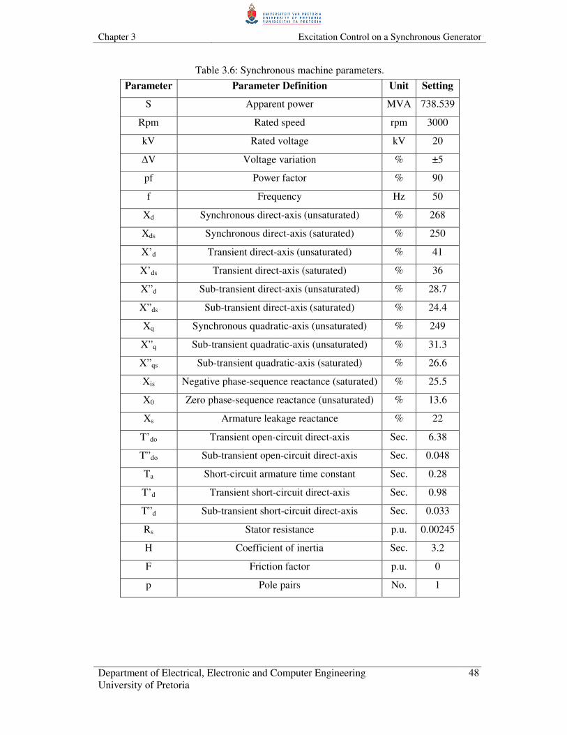
Chapter 3 Excitation Control on a Synchronous Generator
Department of Electrical, Electronic and Computer Engineering
University of Pretoria
48
Table 3.6: Synchronous machine parameters.
Parameter Parameter Definition Unit Setting
S Apparent power MVA 738.539
Rpm Rated speed rpm 3000
kV Rated voltage kV 20
∆V Voltage variation % ±5
pf Power factor % 90
f Frequency Hz 50
Xd Synchronous direct-axis (unsaturated) % 268
Xds Synchronous direct-axis (saturated) % 250
X’d Transient direct-axis (unsaturated) % 41
X’ds Transient direct-axis (saturated) % 36
X”d Sub-transient direct-axis (unsaturated) % 28.7
X”ds Sub-transient direct-axis (saturated) % 24.4
Xq Synchronous quadratic-axis (unsaturated) % 249
X”q Sub-transient quadratic-axis (unsaturated) % 31.3
X”qs Sub-transient quadratic-axis (saturated) % 26.6
Xis Negative phase-sequence reactance (saturated) % 25.5
X0 Zero phase-sequence reactance (unsaturated) % 13.6
Xs Armature leakage reactance % 22
T’do Transient open-circuit direct-axis Sec. 6.38
T”do Sub-transient open-circuit direct-axis Sec. 0.048
Ta Short-circuit armature time constant Sec. 0.28
T’d Transient short-circuit direct-axis Sec. 0.98
T”d Sub-transient short-circuit direct-axis Sec. 0.033
Rs Stator resistance p.u. 0.00245
H Coefficient of inertia Sec. 3.2
F Friction factor p.u. 0
p Pole pairs No. 1

Chapter 3 Excitation Control on a Synchronous Generator
Department of Electrical, Electronic and Computer Engineering
University of Pretoria
49
Table 3.7: Assumed synchronous machine parameters.
Parameter Parameter Definition Unit Setting
X’q Transient quadratic-axis (unsaturated) % 26.2
T’qo Transient open-circuit direct-axis Sec. 1.1
T”qo Sub-transient open-circuit direct-axis Sec. 0.081
T’so Transient short-circuit direct-axis Sec. 1.0
T”so Sub-transient short-circuit direct-axis Sec. 0.035
To validate the simulation model, a field measurement recorded during a step-change was
used to set up the exciter settings of the simulation model. Using standard settings, k1 =
100, k2 = 10000 and k3 = 0.02, a model was developed to determine the excitation settings
such that the response of the simulation model matches that of the field recording. Figure
3.24 shows the recorded stator voltage (5V = Vnominal). A step change of 10% was
recorded from 105% to 95% and from 95% to 105%. The results of the simulated step
response tests can be seen in Figure 3.25 and Figure 3.26 for upwards and downwards
step-changes. The resultant excitation settings for the model can be seen in Table 3.8.
These settings were used for all the simulations.
0 0.5 1 1.5 2 2.5 3
x 104
4.6
4.7
4.8
4.9
5
5.1
5.2
5.3
5.4
Time (ms)
Volta
ge (
pu)
Stator Voltage
Figure 3.24: Actual stator voltage measured for a 10% step-change in magnitude.

Chapter 3 Excitation Control on a Synchronous Generator
Department of Electrical, Electronic and Computer Engineering
University of Pretoria
50
Table 3.8: Automatic voltage regulator setting parameters.
Parameter Parameter Definition Unit Parameter Setting
VRmax Max. value of the regulator output voltage p.u. 6.43
VRmin Min. value of the regulator output voltage p.u. -6
VImax Max. internal signal within voltage regulator p.u. 10
VRmin Min. internal signal within voltage regulator p.u. -10
KA Regulator gain p.u. 39
KC Regulator gain p.u. 0.038
KF Regulator stabilizing circuit gain p.u. 0
TA Regulator amplifying time constant Sec. 0
TB Voltage regulator amplifying time constant Sec. 1
TC Voltage regulator amplifying time constant Sec. 1
TF Regulator stabilizing circuit time constant Sec. 0
TR Regulator input filter time constant Sec. 0.04
Ifd Excitation field current p.u. Variable
6000 7000 8000 9000 10000 11000 12000 13000
4
4.2
4.4
4.6
4.8
5
5.2
5.4
5.6
Time (ms)
Volta
ge
Recorded Field Voltage
Simulated Terminal Voltage
Figure 3.25: Stator voltage measured compared to a simulated response.
Figure 3.25 shows the response of the recorded field stator voltages compared to the
simulated response of the synchronous generator using the ST1 static excitation and the
algorithm model for a step-change from 105% to 95%.

Chapter 3 Excitation Control on a Synchronous Generator
Department of Electrical, Electronic and Computer Engineering
University of Pretoria
51
1.15 1.2 1.25 1.3 1.35 1.4 1.45 1.5 1.55
x 104
4
4.2
4.4
4.6
4.8
5
5.2
5.4
5.6
Time (ms)
Volta
ge (
pu)
Recorded Field Voltage
Simulated Terminal Voltage
Figure 3.26: Stator voltage measured compared to a simulated response.
Figure 3.26 shows the response of the recorded field stator voltages compared to the
simulated response of the synchronous generator using the ST1 static excitation and the
algorithm model for a voltage step-change of 95% to 105%.
Figure 3.25 and Figure 3.26 show that the simulation model using the ST1 exciter with the
standard algorithm has a step-change response characteristic that is very close to the
measured voltage step-change characteristic.
3.8 GENERATOR RESPONSE USING BOTH METHODS AS INPUT TO THE
AVR
3.8.1 Introduction
Eight tests were conducted comparing the algorithm and the diode bridge rectifier for the
tracking of the terminal voltage as input to the excitation model. The simulations tested the
response of the generator against reactive load changes. Eight different loading conditions
were simulated. This resulted on a reduction or increase on the generator terminal voltage
by stepping the reactive power through load 2. The loading conditions are shown in Table
3.9. Reactive loading has the largest influence on the generator’s terminal voltage, hence
this was used. The mechanical torque on the generator input was kept constant at 0.277pu
for all studies.

Chapter 3 Excitation Control on a Synchronous Generator
Department of Electrical, Electronic and Computer Engineering
University of Pretoria
52
Table 3.9: Loading conditions for the eight studies.
Study
No.
Load 1
Active Power
(MW)
Load 1
Reactive Power
(MVAr)
Load 2
Active Power
(MW)
Load 2
Reactive Power
(MVAr)
1 400 20 10 50
2 400 20 10 100
3 400 20 10 200
4 400 20 10 300
5 400 20 10 50
6 400 20 10 100
7 400 20 10 200
8 400 20 10 300
3.8.2 Algorithm Model Simulation Tests
Two models of the algorithm were used. Algorithm Model 1 has the original parameter
settings as per [1]. Algorithm Model 2 has the customized parameter settings to optimize
the response of the synchronous generator. The model shown in Figure 3.21 was used for
all the simulations.
3.8.3 Diode Bridge Rectifier Model
One diode bridge rectifier model was developed. The model shown in Figure 3.22 was
used for all the simulations.
3.8.3 Performance and Results
For studies 1 to 4 the breaker was closed and the load was switched in. For studies 5 to 8
the breaker was opened and the load switched off. Following the change in the load, the
AVR regulates the terminal voltage to within 1.5% of 1pu. The simulated response time of
the synchronous generator was taken when the voltage was regulated to within 2% of the
nominal after the load was switched.
The resultant terminal voltages of both methods were tracked by the same algorithm
model. The resultant response is shown in Table 3.10. This was done to compare the
response of the two models with the same method. Figure 3.27 shows a graphical

Chapter 3 Excitation Control on a Synchronous Generator
Department of Electrical, Electronic and Computer Engineering
University of Pretoria
53
representation of the response times. The graphical results for Test 4 and Test 8 for the
Algorithm 2 and the DBR are shown. The results for Test 4 and Test 8 are shown through
Figures 3.27 to 3.35. The resultant peak (reactive load switched out) and dip (reactive load
switched in) terminal voltage profiles is due to the time it take the exciter model to react to
the new reactive power level as well as the high inductance of the generator field windings,
making it difficult to make rapid changes in field current and a moment of over and under
excitation occur resulting in the peak and dip voltage profiles.
Table 3.10: Response times of the terminal voltage synchronous generator.
Test No. Algorithm Model 1 Algorithm Model 2 Diode Bridge Rectifier
Model
1 149.6 119.1 177
2 280.1 249 300.6
3 407.9 336.3 383.3
4 548.9 388.4 433.5
5 Not going outside 2% Not going outside 2% 168.2
6 221.3 182.6 263.1
7 285.1 264.3 302.8
8 306.5 282.6 310.7
0
100
200
300
400
500
600
1 2 3 4 5 6 7 8
TIM
E (
ms
)
STUDY NUMBER
GENERATOR RESPONSE TIMES
Alg Model 1 Alg Model 2 Cap Model
Figure 3.27: Generator response times for changes in the reactive loading.

Chapter 3 Excitation Control on a Synchronous Generator
Department of Electrical, Electronic and Computer Engineering
University of Pretoria
54
Figure 3.28 and Figure 3.29 shows the algorithm tracking the resultant terminal voltage for
Test 4 and Test 8 using Algorithm 2 for excitation control. This is to demonstrate the
response of the synchronous machine during the loading conditions for Test 4 and 8.
14 14.5 15 15.5 16 16.50.85
0.9
0.95
1
1.05
1.1
Time (s)
Volta
ge (
pu)
ALG Tracking Voltage
Terminal Voltage
Figure 3.28: Algorithm tracking the resultant terminal voltage for Test 8.
14 14.5 15 15.5 16 16.50.8
0.85
0.9
0.95
1
1.05
1.1
Time (s)
Volta
ge (
pu)
ALG Tracking Voltage
Terminal Voltage
Figure 3.29: Algorithm tracking the resultant terminal voltage for Test 4.

Chapter 3 Excitation Control on a Synchronous Generator
Department of Electrical, Electronic and Computer Engineering
University of Pretoria
55
Figure 3.30 and Figure 3.31 show the frequency and excitation responses using Algorithm
2 for excitation control during the same tests.
0 2 4 6 8 10 12 14 16 18 2040
42
44
46
48
50
52
54
56
58
60
Time (s)
Fre
quency (
Hz)
ALG Test 8, Reactive Load Switched Out
ALG Test 4, Reactive Load Switched In
Figure 3.30: Frequency response using Algorithm 2 for Test 4 and Test 8.
0 2 4 6 8 10 12 14 16 18 20-10
-8
-6
-4
-2
0
2
4
6
8
10
Time (s)
Volta
ge (
pu)
Excitation Voltage for Load Increase
Excitation Voltage for Load Decrease
Figure 3.31: Excitation voltage response using Algorithm 2 for Test 4 and Test 8.

Chapter 3 Excitation Control on a Synchronous Generator
Department of Electrical, Electronic and Computer Engineering
University of Pretoria
56
Figure 3.32 and Figure 3.33 show the algorithm tracking the resultant terminal voltage for
Test 4 and Test 8 using the DBR for excitation control. This is to demonstrate the response
of the synchronous machine during the loading conditions for Test 4 and 8.
14 14.5 15 15.5 16 16.50.85
0.9
0.95
1
1.05
1.1
Time (s)
Volta
ge (
pu)
ALG Tracking Voltage
Terminal Voltage
Figure 3.32: DBR tracking the resultant terminal voltage for Test 8.
14 14.5 15 15.5 16 16.50.8
0.85
0.9
0.95
1
1.05
1.1
Time (s)
Volta
ge (
pu)
ALG Tracking Voltage
Terminal Voltage
Figure 3.33: DBR tracking the resultant terminal voltage for Test 4.

Chapter 3 Excitation Control on a Synchronous Generator
Department of Electrical, Electronic and Computer Engineering
University of Pretoria
57
Figure 3.34 and Figure 3.35 show the frequency and excitation response using the DBR for
excitation control. The rotor speed results in Figures 3.30 and 3.34, shows that the
switching of a reactive load did not have a significant influence on the frequency of the
machine.
0 2 4 6 8 10 12 14 16 18 2040
42
44
46
48
50
52
54
56
58
60
Time (s)
Fre
quency (
Hz)
Cap Test 8, Reactive Load Switched Out
Cap Test 4, Reactive Load Switched In
Figure 3.34: Frequency response using the DBR for Test 4 and Test 8.
0 2 4 6 8 10 12 14 16 18 20-10
-8
-6
-4
-2
0
2
4
6
8
10
Time (s)
Volta
ge (
pu)
Excitation Voltage for Load Increase
Excitation Voltage for Load Decrease
Figure 3.35: Excitation voltage response using the DBR for Test 4 and Test 8.
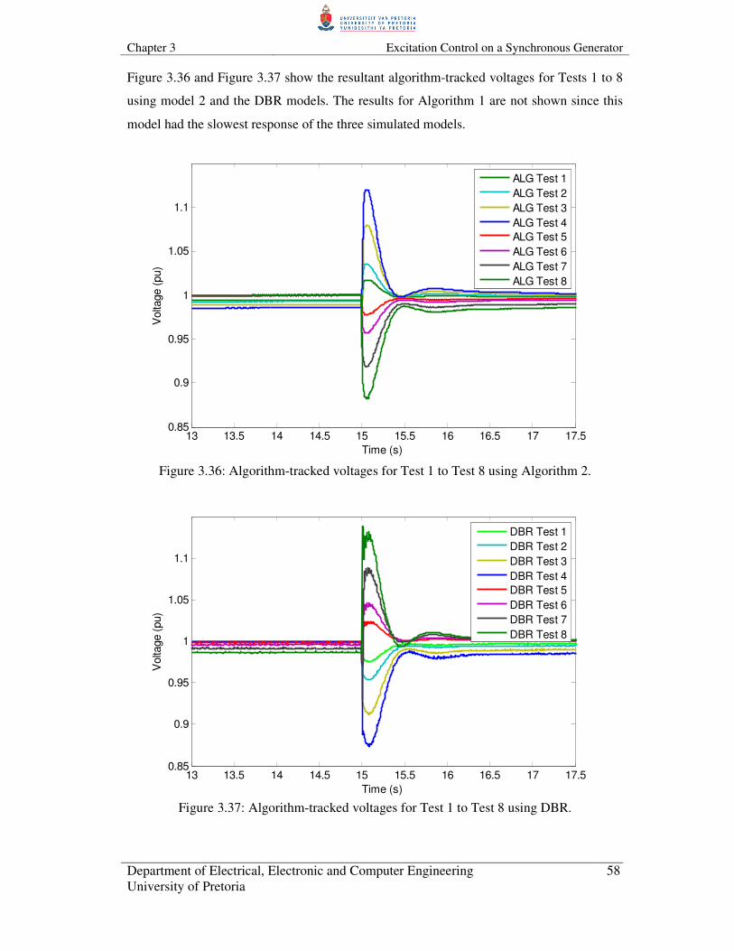
Chapter 3 Excitation Control on a Synchronous Generator
Department of Electrical, Electronic and Computer Engineering
University of Pretoria
58
Figure 3.36 and Figure 3.37 show the resultant algorithm-tracked voltages for Tests 1 to 8
using model 2 and the DBR models. The results for Algorithm 1 are not shown since this
model had the slowest response of the three simulated models.
13 13.5 14 14.5 15 15.5 16 16.5 17 17.50.85
0.9
0.95
1
1.05
1.1
Time (s)
Volta
ge (
pu)
ALG Test 1
ALG Test 2
ALG Test 3
ALG Test 4
ALG Test 5
ALG Test 6
ALG Test 7
ALG Test 8
Figure 3.36: Algorithm-tracked voltages for Test 1 to Test 8 using Algorithm 2.
13 13.5 14 14.5 15 15.5 16 16.5 17 17.50.85
0.9
0.95
1
1.05
1.1
Time (s)
Volta
ge (
pu)
DBR Test 1
DBR Test 2
DBR Test 3
DBR Test 4
DBR Test 5
DBR Test 6
DBR Test 7
DBR Test 8
Figure 3.37: Algorithm-tracked voltages for Test 1 to Test 8 using DBR.
Chapter 3 Excitation Control on a Synchronous Generator
Department of Electrical, Electronic and Computer Engineering
University of Pretoria
59
From the simulations it was found that the response of the synchronous generator is not
always directly proportional to the speed of the tracking device. The AVR responds faster
to the error signal than to the direct tracking of the feedback signal. It was also found that
the algorithm tracked the terminal voltage more accurately if a low-pass filter with a cut-
off frequency of 80Hz was used. The low-pass filter adds a time delay on the tracked
voltage, but the resultant waveform is more stable.
3.9 SUMMARY OF RESULTS
The presentation and performance of the proposed method of tracking a synchronous
generator’s terminal voltage was compared to a more common method. With reference to
the discussions presented throughout this chapter, the main features of the proposed
method can be summarized as follows:
• Comparison between the algorithm and the diode bridge rectifier to track step
changes in the voltage magnitude shows a vast improvement in the steady-state
error using the algorithm. The proposed method has a steady state error of less than
1%, whilst the diode bridge rectifier has a steady state error of 4%.
• Comparison between the algorithm and the diode bridge rectifier to track step
changes in the voltage magnitude shows a vast improvement in the speed of
response using the algorithm. The algorithm has a response time of less than 10ms
to the new nominal value, whilst the diode bridge rectifier has a response time of
120ms.
• Using both methods for AVR under different loading conditions on a synchronous
generator delivered satisfactory results in terms of accuracy and speed of response.
• The optimized algorithm model showed an improvement over the diode bridge
rectifier in the accuracy and speed of the response of the synchronous generator.
3.10 CONCLUDING REMARKS
In this chapter a method of tracking a generator’s terminal voltage magnitude for excitation
control is presented. The method was first compared to an existing diode bridge rectifier
method of tracking step changes in voltage magnitude. Both methods were then applied to
track synchronous generator terminal voltage for AVR under changing reactive load
conditions. The studies were conducted to determine whether the algorithm can respond

Chapter 3 Excitation Control on a Synchronous Generator
Department of Electrical, Electronic and Computer Engineering
University of Pretoria
60
fast and accurate enough to be able to be applied as a method of voltage tracking for AVR
purposes under steady state conditions.
A basic diode bridge rectifier model was built in Matlab Simulink and compared to the
algorithm model. The result for comparing the accuracy and response of both methods for
step changes in magnitude shows that the algorithm responds faster and more accurate than
the diode bride rectifier.
Synchronous generator machine data was obtained along with a field measurement of the
terminal voltage under step change conditions showing the response characteristic of the
synchronous generator. A model containing the synchronous generator with an IEEE ST1
exciter model along with the algorithm to track the terminal voltage was built. The exciter
settings were customized until the software model’s response matched that of the field
measurement. This model used in comparing the algorithm and the diode bridge rectifier in
tracking of the terminal voltage for input to the AVR.
Both methods display stability and satisfactory performance to sufficiently control the
generator terminal voltage. The terminal voltage was controlled within 1.5% before and
after the reactive power load had respectively been switched on and off. It was seen that
the biggest voltage dip, 12%, was experienced in Test 4 with a response time of less than
half a second. The highest peak voltage, 12.2%, was experienced in Test 8 with the
response times being around 300ms for both methods. The exciter and machine responded
faster for decrease in reactive power, decrease in field current, than an increasing in
reactive power, increase in field current. This was due to the fact that the performance of
the synchronous generator is governed by the high synchronous reactance Xd.
A comparison between the field voltages of both methods showed a very good relation
with almost identical characteristics. Although the performance of the algorithm in terms
of tracking the voltage was quicker than the diode bridge rectifier as shown in Chapter 1,
the end result in the response of the synchronous generator was seen to be insignificant.

Chapter 4 Application of the Algorithm to Voltage Dip Mitigation
Department of Electrical, Electronic and Computer Engineering
University of Pretoria
61
CHAPTER 4
APPLICATION OF THE ALGORITHM TO VOLTAGE DIP MITIGATION
4.1 INTRODUCTION
Generally speaking electrical equipment prefers a constant RMS voltage. Power quality
has been the focus of considerable research in recent years, with voltage dips in particular
causing expensive downtime. Voltage dips of only a few tenths of a second can cause
production losses. This can result in expensive downtime.
Voltage dips are defined as a decrease in the RMS voltage at the power frequency for
durations from 0.5 cycles to 1 minute [9]. A 200ms 25% voltage dip is shown in Figure
4.1. The duration of a voltage dip is the time measured from the moment the RMS voltage
drops below 0.9pu of the nominal voltage to when the voltage rises to above 0.9pu of the
nominal voltage again. Voltage dips are common in power systems and are typically
caused by switching operations that are associated either with a temporary disconnection of
supply, flow of inrush currents or fault currents.
Voltage dips are impossible to prevent, but it is possible to mitigate the impact on the
power system and thus limit the damage to equipment. In this chapter the nonlinear filter is
used to track the voltage magnitude of the supply voltage. This tracked magnitude is used
to detect voltage dips. Although mitigation techniques do exist, the deciding factor that
could prevent catastrophic failure is the time required to detect the dip. Damage caused by
voltage dips can be reduced by either increasing the immunity of the effected equipment
against voltage dips or increasing the fault level of the power system. The algorithm is
incorporated in dip detection and is used in a control system to help mitigate voltage dips.
The criteria for equipment designed or used for voltage dip mitigation are the following:
• The detection and control equipment of a mitigation device must be accurate, fast
and sensitive to be able to sense the voltage dip as fast as possible to be able to
react and operate as fast as possible to mitigate the dip.
• The device must be able to improve the power system voltage.
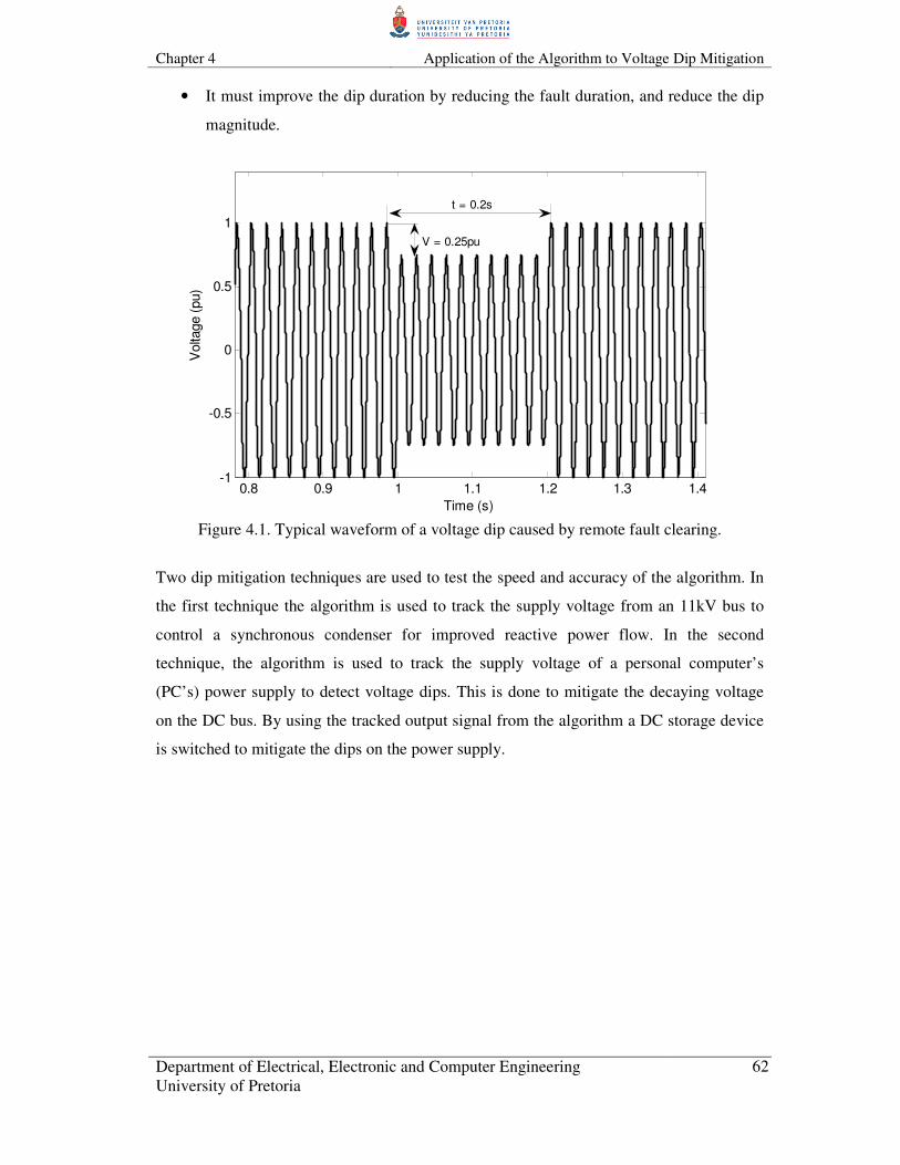
Chapter 4 Application of the Algorithm to Voltage Dip Mitigation
Department of Electrical, Electronic and Computer Engineering
University of Pretoria
62
• It must improve the dip duration by reducing the fault duration, and reduce the dip
magnitude.
0.8 0.9 1 1.1 1.2 1.3 1.4-1
-0.5
0
0.5
1
Time (s)
Volta
ge (
pu)
V = 0.25pu
t = 0.2s
Figure 4.1. Typical waveform of a voltage dip caused by remote fault clearing.
Two dip mitigation techniques are used to test the speed and accuracy of the algorithm. In
the first technique the algorithm is used to track the supply voltage from an 11kV bus to
control a synchronous condenser for improved reactive power flow. In the second
technique, the algorithm is used to track the supply voltage of a personal computer’s
(PC’s) power supply to detect voltage dips. This is done to mitigate the decaying voltage
on the DC bus. By using the tracked output signal from the algorithm a DC storage device
is switched to mitigate the dips on the power supply.

Chapter 4 Application of the Algorithm to Voltage Dip Mitigation
Department of Electrical, Electronic and Computer Engineering
University of Pretoria
63
4.2 SYNCHRONOUS CONDENSER CONTROL
4.2.1 Basic Synchronous Condenser Theory
A synchronous condenser shares much of its architecture with the synchronous generator.
It is a synchronous machine operating without a prime mover or a mechanical load. By
controlling the field excitation it can either absorb or generate reactive power. An AVR
can automatically adjust the reactive power output to maintain the terminal voltage at a set
point. A small amount of active power is drawn from the system to supply the losses in the
synchronous condenser.
A synchronous condenser is used to reduce the effective supply impedance at a busbar to
which the synchronous condenser is connected. The synchronous condenser reduces the
effective impedance between the supply “infinite bus” by virtue of paralleling the
synchronous condenser transient reactance in series with the synchronous condenser air-
gap EMF. This will then result in the network supply impedance being in series with the
network “infinite bus” reactance. This will reduce the magnitude of the voltage dip.
Synchronous condensers are usually connected to a network through either its own
transformer, or through the tertiary winding of a three-winding transformer [16 - 18].
Synchronous condensers are an attractive source of dynamic VAR compensation, either
inductive or capacitive. This can be used to improve system stability and maintain voltages
under varying load conditions and contingencies. Dynamic VARs are an important
requirement for increasing the electric loading of transmission lines. Although static
capacitors are widely used for this function, a dynamic response is often required to
maintain voltage stability for the prevention of voltage dips or voltage collapse. Reactive
power does not provide useful energy for the load, but it is a necessary requirement for the
AC power grids. As the power demand increases over an AC line, the need for reactive
power also increases rapidly. The deficiency of reactive power can limit the amount of real
power that can be delivered across a long transmission line. This can cause voltage
regulation problems. It is an advantage to produce the necessary reactive power close to
the loads.

Chapter 4 Application of the Algorithm to Voltage Dip Mitigation
Department of Electrical, Electronic and Computer Engineering
University of Pretoria
64
4.2.2 Closed Loop Voltage Mitigation Studies
The simulations presented examine the effect that the synchronous condenser has on
voltage dips. The dips are caused by simulating different loading conditions as well as
faults on the network. The proposed technique is used to track the terminal voltage on an
11kV busbar and using the reference signal as control signal input into the AVR. The
voltage dip waveforms are analyzed with and without the synchronous condenser
connected to the network. The algorithm and AVR were used to control the field voltage.
The simulated network consists of two 100km, 400kV lines. One line is connected to a
constant load and the other to a 132kV network through a 400/132kV transformer. The
132kV network consists of two 20km lines, one connected to a constant load and the other
connected to the 11kV network through two 132/11kV transformers. The one transformer
is connected to a constant load, with the other connected through a transformer to the
synchronous condenser.
Figure 4.2 shows the simulated network with the faults that were applied to the network.
The 400kV three-phase fault was applied for 100ms. A 132kV three-phase fault and 11kV
three–phase fault was applied for 400ms and one second respectively. The fault and
loading conditions were used to simulate voltage dips on the network. The algorithm was
used to the busbar voltage rapidly and accurately to control the synchronous condenser’s
reactive power delivery to the network. This was applied under steady-state as well as fault
conditions.
Two types of studies were performed to test the synchronous condenser’s voltage
mitigation performance under various conditions. The first set of studies was to test the
performance under the changing load conditions on the network. For this an active load
with a power factor of 0.70 inductive (to increase the reactive power component on the
network) was switched on the 132kV network. The second set of studies was to test the
performance of the synchronous machine and its control system for multiple faults on the
network.

Chapter 4 Application of the Algorithm to Voltage Dip Mitigation
Department of Electrical, Electronic and Computer Engineering
University of Pretoria
65
-K-
Volts > pu2
-K-
Volts > pu1
v +-
Voltmeter2
v +-
Voltmeter1
A
B
C
Static 400kV 51MVA Load
A
B
C
Static 132kV 51MVA Load
A
B
C
Static 11kV 11.2MVA Load
0
Mechanical Torque
Field Voltage
In1
In2
Out1
Excitation System
In1Out1
Algorithm
A
B
C
400kV Infinite Bus
A
B
C
A
B
C
400kV Fault
A
B
C
a
b
c
400/132kV
Transformer
Pm
Vf_
m
A
B
C
20MVA Synchronous
Condenser
A
B
C
A
B
C
132kV Fault A
B
C
a
b
c
132/11kV
Transformer 2
A
B
C
a
b
c
132/11kV
Transformer 1
A
B
C
a
b
c
13.8/11kV
Condenser
Transformer
11kV Voltage
A
B
C
A
B
C
11kV Fault
100km 400kV Line1
100km 400kV Line
100km 132kV Line3
100km 132kV Line2
A B C
10 kW
Static Load
<Rotor speed wm (pu)>
<Output reactive power Qeo (pu)>
Figure 4.2: Simulated network with the synchronous condenser.
Under steady-state conditions with the condenser not connected, the voltage drop from the
400kV source to the 11kV busbar is approximately 1.44%. The voltage on the 400kV
busbar is 1pu and at the 11kV busbar 0.9856 p.u. This is within the allowed limit of 5%.
This was achieved without the use of tap position changers to correct the voltage on the
low voltage sides of the transformers. With the condenser connected, the 11kV busbar
voltage was brought up to 1 p.u.
Figure 4.3 shows the profile of the field voltage applied to the synchronous condenser to
keep the 11kV busbar voltage at 1pu. Figure 4.4 and Figure 4.5 show the rotor speed and
reactive power delivery profiles of the synchronous condenser. This shows that the
machine is stable when regulating the rotor speed and reactive power delivery to regulate
the 11kV busbar voltage at 1pu. The rotor speed is kept at 1pu. The reactive power
stabilizer is set at 0.07pu to keep the 11kV voltage at 1pu. The field voltage and the

Chapter 4 Application of the Algorithm to Voltage Dip Mitigation
Department of Electrical, Electronic and Computer Engineering
University of Pretoria
66
resultant reactive power increases rapidly as the reactive loading increases and when faults
are applied to the network.
0 2 4 6 8 10 12 14 16 18 20-1
0
1
2
3
4
5
6
Time (s)
Volta
ge (
pu)
Figure 4.3: Synchronous condenser field voltage.
0 2 4 6 8 10 12 14 16 18 200
0.2
0.4
0.6
0.8
1
1.2
1.4
1.6
1.8
2
Time (s)
Speed (
pu)
Figure 4.4: Synchronous condenser rotor speed.

Chapter 4 Application of the Algorithm to Voltage Dip Mitigation
Department of Electrical, Electronic and Computer Engineering
University of Pretoria
67
0 2 4 6 8 10 12 14 16 18 20-1.5
-1
-0.5
0
0.5
1
1.5
2
2.5
3
Time (s)
Reactiv
e P
ow
er
(pu)
Figure 4.5: Synchronous condenser reactive power delivery.
4.2.3. Simulations for Changes in Loading Conditions
Additional loads were connected to the existing 132kV load through control of circuit
breaker. This changes the reactive power demand on the network. Figure 4.6 shows the
waveforms on the 11kV side with and without the synchronous condenser connected. No
faults are applied. The additional load is switched on the 132kV network. Without the
condenser connected to the 11kV network, a constant voltage drop (network volt drop) of
1.44% occurs. The volt drop increases to 4.12% as the load is switched on the 132kV
network. The load is switched on at 10 seconds and switched off at 15 seconds.

Chapter 4 Application of the Algorithm to Voltage Dip Mitigation
Department of Electrical, Electronic and Computer Engineering
University of Pretoria
68
8 9 10 11 12 13 14 15 16 17 18
0.94
0.96
0.98
1
1.02
1.04
Time (s)
Votla
ge (
pu)
11kV Busbar voltage without Condenser
11kV Busbar voltage with Condenser
Figure 4.6: Voltage waveforms for additional loading.
This figure shows how effectively the AVR of the synchronous condenser regulates the
voltage on the 11kV busbar. The 11kV voltage does not dip by more than 2% after the load
is switched in. It does not rise more than 2% after the load is switched out. The algorithm
and AVR are found to be stable under all the test loading conditions. Further tests were
conducted to test the algorithm under fault conditions. These tests are discussed in the next
section.
4.2.4 Voltage Dip Mitigation under Fault Conditions on the Network
Faults on three different locations were simulated. The faults were located on different
network voltage levels with varying fault times used to quantify the voltage dip on the
11kV network with and without the synchronous condenser connected. The fault locations
used in the three studies are shown in Figure 4.2.
4.2.4.1 400kV Three Phase to Ground Fault Simulations
Figure 4.7 shows the resultant waveforms of the 11kV busbar for a 100ms fault on the
400kV network. The voltage dips to approximately 0.555 p.u. without the condenser
connected. With the condenser connected, the voltage dips to 0.717 p.u. Voltage support of
16.2% is obtained with the condenser connected.

Chapter 4 Application of the Algorithm to Voltage Dip Mitigation
Department of Electrical, Electronic and Computer Engineering
University of Pretoria
69
14.7 14.8 14.9 15 15.1 15.2 15.3 15.40.3
0.4
0.5
0.6
0.7
0.8
0.9
1
1.1
1.2
1.3
Time (s)
Votla
ge (
pu)
11kV Busbar voltage with condenser
11kV Busbar voltage without condenser
Figure 4.7: 11kV voltage profiles for a 400kV fault.
4.2.4.2 132kV Three-Phase to Ground Fault Simulations
Figure 4.8 shows the resultant voltage waveforms on the 11kV busbar for a 400ms fault on
the 132kV network. The voltage dips to 0.468 p.u. without the condenser connected. With
the condenser connected the voltage dips to 0.655 per unit, with the voltage eventually
recovering to 0.671 p.u. A voltage support of 18.7% is obtained with the condenser
connected.

Chapter 4 Application of the Algorithm to Voltage Dip Mitigation
Department of Electrical, Electronic and Computer Engineering
University of Pretoria
70
14 14.5 15 15.5 16 16.50.3
0.4
0.5
0.6
0.7
0.8
0.9
1
1.1
1.2
1.3
Time (s)
Votla
ge (
pu)
11kV Busbar voltage with condenser
11kV Busbar voltage without condenser
Figure 4.8: 11kV voltage profiles for a 132kV fault.
4.2.4.3 11kV Three-Phase to Ground Fault Simulations
Figure 4.9 shows the resultant voltage waveforms on the 11kV busbar for a one second
fault on the 11kV network. The voltage dips to 0.9116 p.u. without the condenser
connected. With the condenser connected the voltage dips to approximately 0.945 p.u.
Voltage support of 5.9% is obtained with the condenser connected.
13 14 15 16 17 180.8
0.85
0.9
0.95
1
1.05
1.1
Time (s)
Volta
ge (
pu)
11kV Busbar voltage with condenser
11kV Busbar voltage without condenser
Figure 4.9: 11kV Voltage Profiles for a 11kV Fault.
Chapter 4 Application of the Algorithm to Voltage Dip Mitigation
Department of Electrical, Electronic and Computer Engineering
University of Pretoria
71
4.2.5 Summary of Results
The performance of the proposed method of tracking a network’s busbar voltage as a
reference point for reactive power control is presented. With reference to the discussions
presented throughout this chapter, the main features of the proposed method can be
summarized as follows:
• The algorithm showed good stability, speed and accuracy in tracking the network
voltage for reactive load changes on the 132kV network. The synchronous
condenser can control the network voltage to within 2%. An improvement of more
than 2% is experienced when the load is added onto the network.
• The proposed method is stable, fast and accurate in tracking the network voltage for
a three-phase fault on the 400kV network. An improvement of 16% on the dip
magnitude is obtained.
• Network voltage for a three phase fault on the 132kV network was tracked. An
improvement of 18% on the dip magnitude is obtained.
• Network voltage for a three phase fault on the 11kV network was tracked. An
improvement of 6% on the dip magnitude is obtained.

Chapter 4 Application of the Algorithm to Voltage Dip Mitigation
Department of Electrical, Electronic and Computer Engineering
University of Pretoria
72
4.3 MITIGATING DECAYING DC BUS VOLTAGES
4.3.1 Introduction
The power supply of a typical computer and other low-power devices normally consists of
a single-phase diode bridge rectifier and a DC-DC voltage regulator. The capacitor
connected to the non-regulated DC bus reduces the voltage ripple at the input to the
voltage regulator. The voltage regulator transforms a non-regulated DC voltage of a few
hundred volts into a regulated DC voltage of around 12V. If the AC voltage drops, the
voltage on the DC side of the rectifier drops. The voltage regulator is able to keep its
output voltage constant over a certain range of the input voltage. If the voltage at the DC
bus is too low, the regulated DC voltage will drop and ultimately errors will occur in the
digital electronics. The protection circuits will trip the device to protect the digital
electronic components at a preset minimum DC bus voltage. If the RMS voltage drops
rapidly, the maximum AC voltage remains less than the DC voltage for the whole cycle.
The capacitor continues to discharge for a few cycles until the capacitor voltage drops
below the maximum AC voltage. A new equilibrium will be reached. The effect of the
voltage drop is discussed in [19].
The discharging of the capacitor is determined by the load connected to the DC bus and not
the AC voltage. Voltage dips causes the same decay in the DC voltage. The duration of the
decay is determined by the magnitude of the dip. The larger the dip, the longer it takes for
the capacitor to charge from the power supply. If the AC voltage remains less than the DC
bus voltage, the electrical energy of the load is supplied from the energy stored in the
capacitor [19].
For a capacitance C, the stored energy, a time t after dip initiation is equal to:
2)(2
1tCV (4.1)
with V(t) the DC bus voltage.
This energy is equal to the energy at dip initiation minus the energy taken by the load:
PtCVCV −= 2
0
2
2
1
2
1 (4.2)

Chapter 4 Application of the Algorithm to Voltage Dip Mitigation
Department of Electrical, Electronic and Computer Engineering
University of Pretoria
73
with V0 the DC bus voltage at the dip initiation and P the loading of the DC bus.
Expression 4.2 holds when the DC bus voltage is higher than the absolute value of the AC
voltage. Solving 4.2 gives an expression for the voltage during this initial decay period:
tC
PVV
22
0 −= (4.3)
The moment the DC bus voltage drops below the absolute value of the AC voltage, the
normal operation mode of the rectifier takes over and the DC bus voltage remains constant
[19].
Applications such as variable speed drives and PC’s are affected by voltage dips. Offline
storage devices can reduce the impacts of a voltage dip. Rapid detection of a voltage dip is
necessary to switch the storage device. This section applies the non-linear filter to rapid
detection of dips so that the offline storage device can be used for mitigation.
4.3.2 Experimental Setup
For the experimental testing of the performance of the algorithm, a voltage dip generator
was used that is capable of generating dips of varying magnitudes and duration. Figure
4.10 shows the experimental setup that was used to conduct the experiments. A
transformer was used with two output voltages. The first output was set at 100% of the
rated voltage. The second output set to the required dip magnitude voltage level. The
transformer has taps that can be set from 40V to 360V in steps of 40V. The PC power
supply was fed through the secondary winding. A TMS320F240 processor was used to log
the required control data and to switch solid state relays very quickly between the two
outputs to obtain the desired dip magnitude and duration. This voltage was then used as the
input voltage to the PC power supply. The rated voltage of the PC power supply was 380V.

Chapter 4 Application of the Algorithm to Voltage Dip Mitigation
Department of Electrical, Electronic and Computer Engineering
University of Pretoria
74
Figure 4.10: Experimental setup for dips on a PC.
Three different types of testing were done to determine the effects of voltage dips on the
PC. The first test was done in order to test the time in which the PC can operate under no
load conditions for a voltage dip. The second test was used to test the time in which the PC
can operate under a 100% CPU load with additional auxiliaries powered. The auxiliary that
was used is the CD-ROM. For the third test, a solid state switch that is coupled in series
with a capacitor was used as a storage device. A discharge resistor was installed on the DC
bus as shown in Figure 4.10. This simulates offline storage. The input voltage, V1, was
sensed through the processor and was input into the algorithm. The output of the algorithm
(the tracked voltage magnitude), was used to calculate the percentage dip and to send a
signal to switch on the storage device if the dip reaches 0.9pu. The storage device is
switched off when the voltage was restored to above 0.9pu.
Results for test 1 and test 2 were recorded. The operating time of the PC was compared to
the Computer Business Equipment Manufacturers Association (CBEMA) curve [19]. The
CBEMA curve is used as a voltage tolerance recommendation. The CBEMA curve has
become a de facto standard against which the voltage tolerance of equipment is compared.
It was found that the minimum DC bus voltage that is allowed for normal operation of the
power supply is 180V DC. When the DC bus voltage dropped below the 180V DC
threshold, the power supply’s protection tripped and the power supply was reset.

Chapter 4 Application of the Algorithm to Voltage Dip Mitigation
Department of Electrical, Electronic and Computer Engineering
University of Pretoria
75
Table 4.1 shows the resultant operating times for different dip types created for tests 1-3.
Figure 4.11 shows the relationship between voltage tolerance performance of the PC power
supply and the CBEMA curve. It shows the performance of a power supply under the
worst possible conditions (test 2). Figure 4.11 shows that the PC power supply does
conform to the standard of the CBEMA curve.
Table 4.1: PC power supply operation response times.
Voltage Dip
Percentage
Operating Time
Test 1 Test 2 Test 3
30% No interruption 240ms No interruption
50% 32ms 15ms 1400ms
70% 32ms 11ms 1400ms
Figure 4.11: CBEMA curve vs. PC power supply.
Figure 4.12 shows a 30% two second voltage dip tracked by the algorithm in test 1. No
interruption of the PC’s operation was found. This shows that the loading on the PC
combined with the dip did not result in the PC being reset. Figure 4.13 shows the supply

Chapter 4 Application of the Algorithm to Voltage Dip Mitigation
Department of Electrical, Electronic and Computer Engineering
University of Pretoria
76
voltage that was tracked by the algorithm for test 1 (a 50% 32ms voltage dip). An
interruption of the PC’s operation was found after 32ms. This shows that the power supply
loading could not prevent the PC from resetting during the dip. The same result was
obtained for a 70% dip.
500 1000 1500 2000 2500 3000 35000.5
0.6
0.7
0.8
0.9
1
1.1
Time (ms)
Volta
ge (
pu)
ALG Tracking Voltage
Supply Voltage
Figure 4.12: Test 1: 30% 2s dip.
500 600 700 800 900 1000 1100 1200 1300 1400 1500 16000
0.2
0.4
0.6
0.8
1
Time (ms)
Volta
ge (
pu)
ALG Tracking Voltage
Supply Voltage
Figure 4.13: Test 1: 50% 32ms dip.

Chapter 4 Application of the Algorithm to Voltage Dip Mitigation
Department of Electrical, Electronic and Computer Engineering
University of Pretoria
77
For Test 2, the Central Processing Unit (CPU) of the PC was loaded to 100%. The CD-
ROM added a further auxiliary loading onto the power supply. The total consumed power
was measured at 190W. Table 4.1 shows that under these conditions, the PC has no
tolerance for the predefined dips and trips in less than one cycle for the 50% and 70%
voltage dips.
For Test 3, the solid state switch with the storage device was connected onto the DC bus.
The capacitor was allowed to charge to the same voltage as the DC bus. The input voltage
was then tracked by the algorithm. When the voltage dipped to below 0.9pu, the capacitor
was switched on and off via the solid state switch that is controlled by the TMS processor.
Figure 4.14 shows the supplied voltage tracked by the algorithm for Test 3 for a 30%
voltage dip with duration of 4s. No interruption of the PC’s operation was found. Figure
4.14 also shows the solid state switch command signal. The capacitor that is switched in
keep the DC bus voltage above the minimum bus voltage. No interruption in the operation
occurs for a 30% dip with the storage device switched on.
500 600 700 800 900 1000 1100 1200 1300 1400 1500 1600-0.2
0
0.2
0.4
0.6
0.8
1
Time (ms)
Volta
ge (
pu)
Switch Signal
ALG Tracking Voltage
Supply Voltage
Figure 4.14: Test 3: 30% 4s dip.
Figure 4.15 and Figure 4.16 show the supplied voltage tracked by the algorithm for Test 3
for a 50% and 70% voltage dip with a duration of 1.4 seconds. The algorithm detects the
voltage dip within a cycle to switch the capacitor in before the PC’s operation can be
interrupted (within 8ms from the inception of the dip). The method detects the dip below

Chapter 4 Application of the Algorithm to Voltage Dip Mitigation
Department of Electrical, Electronic and Computer Engineering
University of Pretoria
78
0.9 p.u. within 3ms to send a signal to the switch. The capacitor was able to sustain the PC
for around 1.4 seconds before the DC voltage dropped to below the minimum DC bus
voltage.
800 1000 1200 1400 1600 1800 2000 2200 2400 2600 28000.3
0.4
0.5
0.6
0.7
0.8
0.9
1
1.1
Time (ms)
Volta
ge (
pu)
Switch Signal
ALG Tracking Voltage
Supply Voltage
Figure 4.15: Test 3: 50% 1.5s dip.
800 1000 1200 1400 1600 1800 2000 2200 2400 2600 2800-0.2
0
0.2
0.4
0.6
0.8
1
Time (ms)
Volta
ge (
pu)
Switch Signal
ALG Tracking Voltage
Supply Voltage
Figure 4.16: Test 3: 70% 1.4s dip.
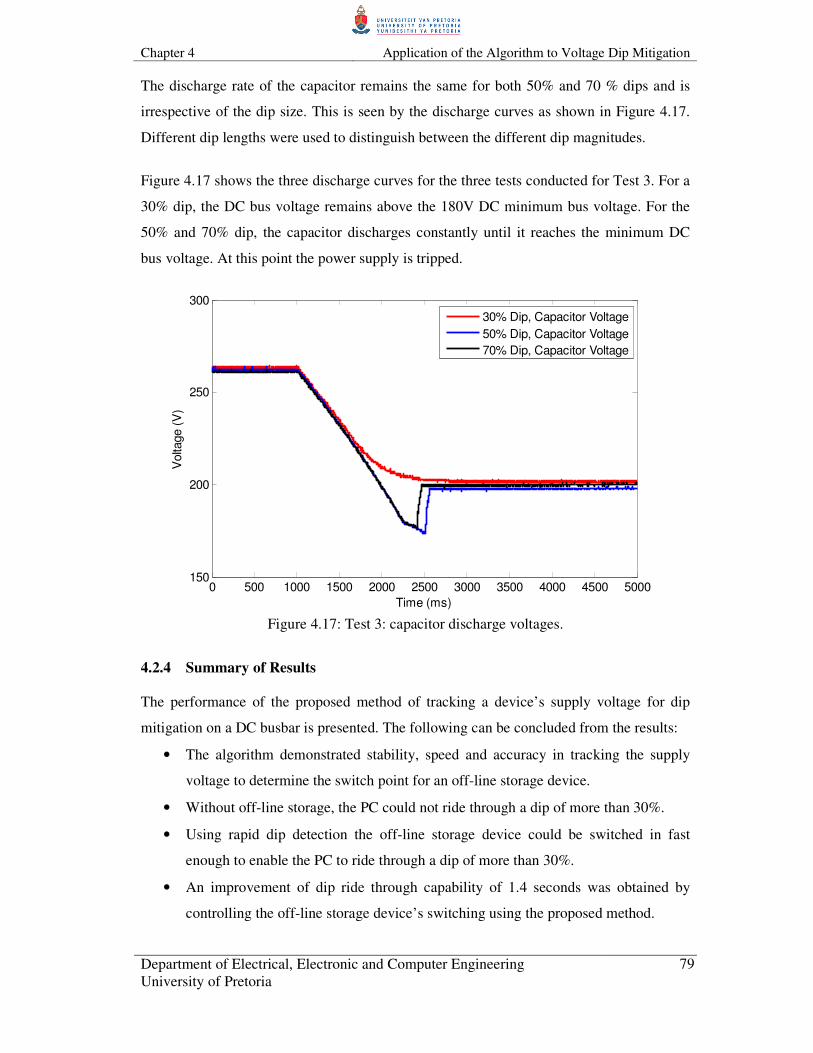
Chapter 4 Application of the Algorithm to Voltage Dip Mitigation
Department of Electrical, Electronic and Computer Engineering
University of Pretoria
79
The discharge rate of the capacitor remains the same for both 50% and 70 % dips and is
irrespective of the dip size. This is seen by the discharge curves as shown in Figure 4.17.
Different dip lengths were used to distinguish between the different dip magnitudes.
Figure 4.17 shows the three discharge curves for the three tests conducted for Test 3. For a
30% dip, the DC bus voltage remains above the 180V DC minimum bus voltage. For the
50% and 70% dip, the capacitor discharges constantly until it reaches the minimum DC
bus voltage. At this point the power supply is tripped.
0 500 1000 1500 2000 2500 3000 3500 4000 4500 5000150
200
250
300
Time (ms)
Volta
ge (
V)
30% Dip, Capacitor Voltage
50% Dip, Capacitor Voltage
70% Dip, Capacitor Voltage
Figure 4.17: Test 3: capacitor discharge voltages.
4.2.4 Summary of Results
The performance of the proposed method of tracking a device’s supply voltage for dip
mitigation on a DC busbar is presented. The following can be concluded from the results:
• The algorithm demonstrated stability, speed and accuracy in tracking the supply
voltage to determine the switch point for an off-line storage device.
• Without off-line storage, the PC could not ride through a dip of more than 30%.
• Using rapid dip detection the off-line storage device could be switched in fast
enough to enable the PC to ride through a dip of more than 30%.
• An improvement of dip ride through capability of 1.4 seconds was obtained by
controlling the off-line storage device’s switching using the proposed method.

Chapter 4 Application of the Algorithm to Voltage Dip Mitigation
Department of Electrical, Electronic and Computer Engineering
University of Pretoria
80
4.4. CONCLUDING REMARKS
From the results it is clear that the proposed method of sensing the magnitude of the
voltage, and using it as input to the AVR, is accurate and fast enough to provide the
synchronous condenser control with good voltage magnitude feedback. The algorithm
displays stability and rapid performance to sufficiently control the condenser. The terminal
voltage is controlled to within 1% before and after the reactive power load has been
switched, as well as before and after the fault applications.
Advances in High Temperature Superconductors (HTS) are enabling a new class of
synchronous rotating machines (Super Motors and Super Generators) that can generally be
categorized as “Super Machines”. Compared to conventional machines of equivalent
rating, these Super Machines are expected to be less expensive, lighter, more compact,
more efficient, and they are expected to provide significantly superior and more stable
operations in a power station. The field windings are made with HTS conductor material
(BSCCO or Bi2223) which operates at 35 – 40 Kelvin and can be cooled with inexpensive
cryo-coolers. The result of this is a machine with a low synchronous reactance (typically
Xd = 0.5 per unit), which assures dynamic stability within its MVA (Mega Voltage-
Amperes) rating and provides better voltage regulation than a conventional machine [17,
18].
The benefits of a lower Xd are summarized as follows:
• The superconducting machine exhibits a lower voltage difference between no-load
and full-load operations.
• The voltage behind the synchronous reactance is only 1.5 per unit at the rated load
at zero power factor (lagging is caused by over-excitation). Since the voltage is
proportional to the field current, the HTS machine can experience a maximum of
50% field current change as compared to a 200% change in a conventional
machine.
• The voltage is 50% less than in a conventional machine.
For synchronous machines the sub-transient reactance (Xd”) can be the same as for
conventional machines, but as for synchronous condensers the Xd” can also be lower
resulting in a much higher per-unit first peak current for a terminal short circuit. With this
new emerging technology the effect of Xd can be minimized and faster tracking methods
can be utilized more effectively through faster excitation response of the synchronous

Chapter 4 Application of the Algorithm to Voltage Dip Mitigation
Department of Electrical, Electronic and Computer Engineering
University of Pretoria
81
condenser. As has already been seen in Chapter 3, although the algorithm tracks the
voltage magnitude faster than the diode bridge rectifier, the effect of Xd minimizes the
effective response of the machine as it is governed by the value of Xd [18].
The algorithm is also applied to detect voltage dips by tracking the input voltage
magnitude of a dc supplying device. The results demonstrates that the algorithm can track
the voltage magnitude rapidly and accurately. It detects the voltage dip quickly enough to
switch a DC energy storage device into the circuit before an interruption in the PC
operation is experienced.
The rapid response of the algorithm to the voltage dip has a distinct advantage in the
mitigation of voltage dips. The time saved by voltage mitigation can be translated into
reducing the component of lost energy during the voltage dip. This can lead to great
savings, not only in operation down-time, but also in component damage due to the low
operating voltage. In the worst case it was shown that the proposed algorithm can detect
voltage dip within 4 ms [9]. The method of testing the algorithm by controlling the
switching of the DC storage device is not presenting a means of voltage mitigation on PC
power supplies. The DC storage device can be switched on continuously with no effect to
the normal operation of the PC, but with the added advantage of having a form of “voltage
dip proofing”. The research only showed that the algorithm can track the voltage
magnitude for dip detection quickly and accurately enough to be used in a similar
application.

Department of Electrical, Electronic and Computer Engineering
University of Pretoria
82
CHAPTER 5
APPLICATION OF THE PROPOSED ALGORITHM FOR REAL-TIME
SYMMETRICAL COMPONENT ESTIMATION
5.1 INTRODUCTION
Power systems are generally three-phase. A power system that is considered to be balanced
has three voltage and current signals with equal magnitudes and 120° phase displacements.
The theory of symmetrical components, developed by C.L. Fortescue in 1918, indicates
that an unbalanced set of signals can be decomposed into three sets of signals. The three
sets are:
• zero sequence, which consists of three phasors with equal magnitudes and 0°
phase-shifts;
• positive sequence, which consists of three phasors with equal magnitudes and 120°
phase-shifts; and
• negative sequence, which consists of three phasors with equal magnitudes and 120°
phase-shifts with the Blue and Yellow phases swopped around from the positive
sequence.
The three sets are shown in Figure 5.1.
Figure 5.1: Zero, positive and negative sequence components.

Chapter 5 Application of the Algorithm for Real-time Symmetrical Component Estimation
Department of Electrical, Electronic and Computer Engineering
University of Pretoria
83
Assuming that the power system operates at a fixed and known frequency, each sequence
component is determined by its magnitude and phase angle. Symmetrical components can
be used in a variety of power system problems such as protection and system modeling [9].
The three components are formulated in terms of a linear matrix transformation involving
the unity complex phasor:
3
2π
αj
e= (5.1)
To express these quantities algebraically, the complex operator α is used. This denotes a
phase shift of +120°.
( )°+∠=×∠ 120)( φαφ II (5.2)
Thus the following values are obtained:
866.05.011201 3
2
jej
+−==°∠=π
α
866.05.024012j−−=°∠=α
(5.3)
Writing the three sequence component equations as separate equations yields the
following:
( )BYR VVVV ++=3
10
( )BYR VVVV2
13
1αα ++=
( )BYR VVVV αα ++= 2
23
1
(5.4)
This chapter studies the proposed method used in [9]. Further experimental studies are
conducted. The proposed method is based on converting the input signals into phasors.
This is done by estimating the magnitude, phase-angle and frequency of the input signal.
From this the sequence components are computed in the time-domain. An overview of the
experimental setup is shown in Figure 5.2. An Omicron 56 three-phase injection set is used
to generate the input signals. The d-Space TMS320F240 processor converts the analog
input signals from the Omicron 56 into digital signals that are input to the PC. As the
magnitude and phase-angles are estimated and made available online, the steady state and

Chapter 5 Application of the Algorithm for Real-time Symmetrical Component Estimation
Department of Electrical, Electronic and Computer Engineering
University of Pretoria
84
dynamic phasors associated with the symmetrical components are also made available in
the frequency and time domain.
Figure 5.2: Experimental setup.
5.2 PERFORMANCE
This section investigates the performance of the proposed system by means of real-time
injection of signals. Following cases are studied:
• Case 1: symmetrical component estimation for step changes in amplitude.
• Case 2: symmetrical component estimation for step changes in phase.
• Case 3: symmetrical component estimation in signals with harmonics.
For each case, the positive sequence component is theoretically calculated and compared to
the performance of the DFT and the proposed method. Comparisons are made in terms of
speed of response and steady state accuracy.

Chapter 5 Application of the Algorithm for Real-time Symmetrical Component Estimation
Department of Electrical, Electronic and Computer Engineering
University of Pretoria
85
5.2.1 Case 1: Effects of a Change in Amplitude
Step in Amplitude
Four case studies were done to compare the DFT and the proposed algorithm model for
changes in the magnitude. The nominal voltage used was 110V (155.56V peak). All results
displayed are in per unit. The four step changes used were the same as in [20]. Step
changes of 0.2pu, 0.4pu, 0.6pu and 0.8pu were tested. The step changes were initiated at 1s
and the voltage was then restored to 1pu at 2s as shown in Figure 5.3. The input voltages
were VA = 1∠0°pu, VB = 0.4∠-120°pu and VC = 1∠120°pu. The theoretical calculated
positive sequence component is V1 = 0.8pu. The resultant DFT and the algorithm model’s
positive sequence components were calculated as V1A = 0.801pu and V1A = 0.803pu
respectively. The resultant zero, positive and negative sequence components for the DFT
and the algorithm model are shown in Figure 5.4 and Figure 5.5.
500 1000 1500 2000 2500
-1
-0.8
-0.6
-0.4
-0.2
0
0.2
0.4
0.6
0.8
1
Time (ms)
Volta
ge (
pu)
Va
Vb
Vc
Figure 5.3: Input waveform
Figure 5.4 and Figure 5.5 show the resultant positive sequence waveforms for the positive
sequence calculated by the DFT and the algorithm model for the 0.6pu step changes.
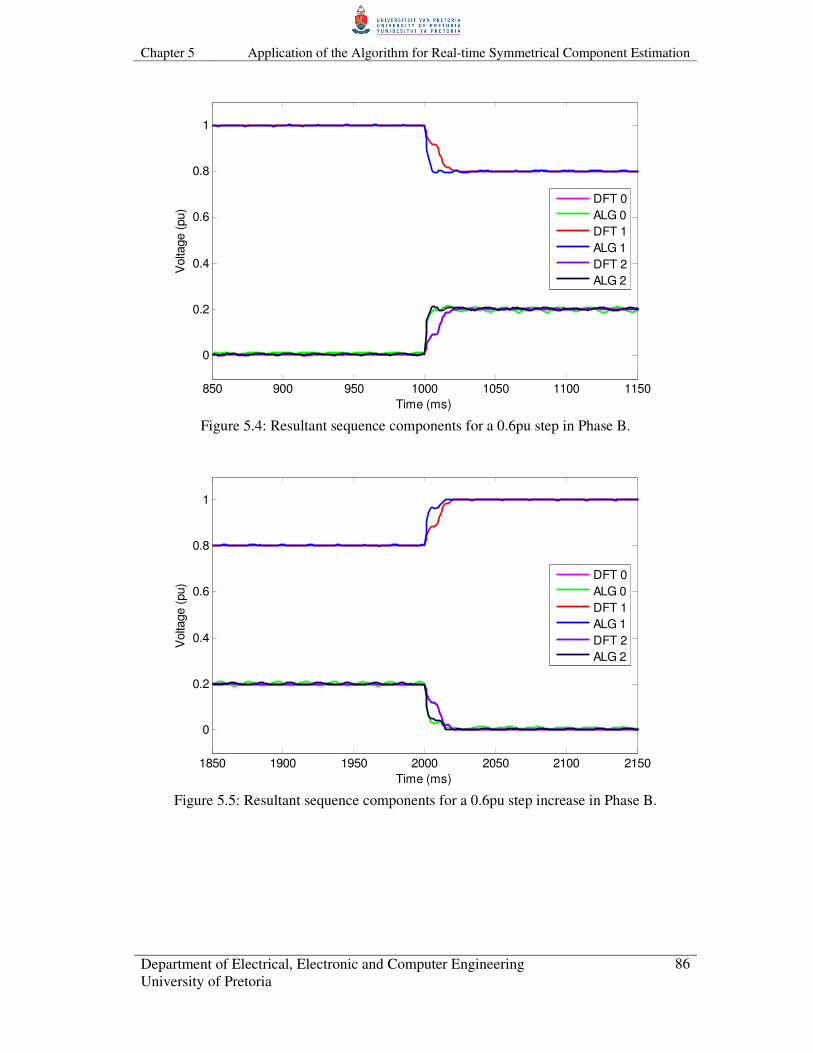
Chapter 5 Application of the Algorithm for Real-time Symmetrical Component Estimation
Department of Electrical, Electronic and Computer Engineering
University of Pretoria
86
850 900 950 1000 1050 1100 1150
0
0.2
0.4
0.6
0.8
1
Time (ms)
Volta
ge (
pu)
DFT 0
ALG 0
DFT 1
ALG 1
DFT 2
ALG 2
Figure 5.4: Resultant sequence components for a 0.6pu step in Phase B.
1850 1900 1950 2000 2050 2100 2150
0
0.2
0.4
0.6
0.8
1
Time (ms)
Volta
ge (
pu)
DFT 0
ALG 0
DFT 1
ALG 1
DFT 2
ALG 2
Figure 5.5: Resultant sequence components for a 0.6pu step increase in Phase B.

Chapter 5 Application of the Algorithm for Real-time Symmetrical Component Estimation
Department of Electrical, Electronic and Computer Engineering
University of Pretoria
87
The results for the varying magnitudes are shown in Table 5.1. The results show
comparisons of the response of the algorithm and the Fourier sequence analyzer to the step
changes in amplitude. It is evident that the algorithm responds quicker to a change in the
amplitude as compared to the Fourier method. The maximum response time difference is
13.48ms on a sampling frequency of 2.5kHz. The steady state error for both methods is
less than 1%.
Table 5.1: Summary of results showing the effects of a step change in magnitude.
Effects of Change in Amplitude
Phase B Step in
Amplitude
% Error Response Time
Difference (ms)
DFT Algorithm
Step
Down
Step
Up
Step
Down
Step
UP
Step Up Step
Down
0.2 0.08 0.12 0.26 0.5 9.31 3.84
0.4 0.18 0.12 0.57 0.45 8.45 5.54
0.6 0.23 0.16 0.36 0.45 13.48 5.04
0.8 0.08 0.12 0.36 0.35 13.01 5.16
Ramp in Amplitude
The effect of a ramp in amplitude is shown in Figure 5.6. A ramp rate of 1pu/sec is used.
The figure shows a comparison between the response of the algorithm and the Fourier
model to a ramp in amplitude of Phase B. The response for both the algorithm and Fourier
models are fast and accurate for the positive and negative sequence components. Although
the algorithm shows improvement over the Fourier model in terms of speed, it has an error
of 2% on the zero sequence component.

Chapter 5 Application of the Algorithm for Real-time Symmetrical Component Estimation
Department of Electrical, Electronic and Computer Engineering
University of Pretoria
88
2500 3000 3500 4000 4500
0
0.2
0.4
0.6
0.8
1
Time (ms)
Volta
ge (
pu)
DFT 0
ALG 0
DFT 1
ALG 1
DFT 2
ALG 2
Figure 5.6: Resultant sequence components for a ramp up and down in Phase B.
5.2.2 Case 2: Effects of a Change in Phase
Step in Phase
Four case studies were done to compare the DFT and algorithm model for changes in
phase angle. The four phase changes tested were a 30°, 60°, 90° and 120° change in the
phase angle of Phase B. The step changes were initiated at 1s and the phase angle was then
restored to 1pu at 2s. Figure 5.7 and 5.8 as show results for a 60° change in angle of Phase
B. The input voltages were VA = 1∠0°pu, VB = 1∠-90°pu and VC = 1∠120°pu. The
theoretical calculated positive sequence component is 0.967pu. The resultant DFT and the
algorithm model’s positive sequence components were calculated as 0.97pu and 0.972pu
respectively.
The results for the varying phase angles are shown in Table 5.2 for step increases and
decreases in the phase angles. The results in Table 5.2 show comparisons of the response
of the algorithm and the Fourier sequence analyzer to phase angle changes. From the
figures it is evident that the proposed method responds faster to a change in the phase angle
as compared to the Fourier method. The maximum response time difference is 10.92ms on
a sampling frequency of 2.5kHz. The steady state error for both methods being less than
1%.

Chapter 5 Application of the Algorithm for Real-time Symmetrical Component Estimation
Department of Electrical, Electronic and Computer Engineering
University of Pretoria
89
Table 5.2: Summary of results showing the effects of a change in the phase angle.
Effects of Change in Phase Angle
Phase B Change
in Phase Angle
% Error Response Time
Difference (ms)
DFT Algorithm
Step
Down
Step
Up
Step
Down
Step
UP
Step Up Step
Down
30° 0.18 0.14 0.36 0.3 7.55 6.3
60° 0.14 0.12 0.68 0.3 10.92 9.64
90° 0.15 0.18 0.67 0.3 10.32 6.8
120° 0.24 0.16 0.69 0.3 8.3 6.34
850 900 950 1000 1050 1100 1150
0
0.2
0.4
0.6
0.8
1
Time (ms)
Volta
ge (
pu)
DFT 0
ALG 0
DFT 1
ALG 1
DFT 2
ALG 2
Figure 5.7: Resultant sequence components for a 60° phase change down in Phase B.

Chapter 5 Application of the Algorithm for Real-time Symmetrical Component Estimation
Department of Electrical, Electronic and Computer Engineering
University of Pretoria
90
1850 1900 1950 2000 2050 2100 2150
0
0.2
0.4
0.6
0.8
1
Time (ms)
Voltage (
pu)
DFT 0
ALG 0
DFT 1
ALG 1
DFT 2
ALG 2
Figure 5.8: Resultant sequence components for a 60° phase change up in Phase B.
Ramp in Phase Angle
The effect of a ramp in the phase angle of Phase B is shown in Figure 5.9. A ramp rate of
80°/sec is used. The figure shows a comparison between the response of the algorithm and
the Fourier model to a ramp in phase angle in Phase B. The response for both the algorithm
and Fourier models are fast and accurate for the positive and negative sequence
components. Although the algorithm shows improvement over the Fourier model in terms
of speed, it has an error of 2% on the zero sequence component.

Chapter 5 Application of the Algorithm for Real-time Symmetrical Component Estimation
Department of Electrical, Electronic and Computer Engineering
University of Pretoria
91
2500 3000 3500 4000 4500
0
0.2
0.4
0.6
0.8
1
Time (ms)
Volta
ge (
pu)
DFT 0
ALG 0
DFT 1
ALG 1
DFT 2
ALG 2
Figure 5.9: Resultant sequence components for a ramp in phase angle of Phase B.
5.2.3 Case 3: Influence of Harmonics
In this case study, the performance of both the Fourier and proposed methods with regard
to harmonic noise on the input signal is demonstrated. The peak amplitudes of the input
signal of Figure 5.10 are VA = 1∠0°pu, VB = 0.6∠-120°pu and VC = 1∠120°pu. When the
frequency of the harmonic is not an exact integer multiple of the fundamental frequency
(inter-harmonic), it poses a problem for the DFT [20]. A 4.5th
inter-harmonic of 0.1pu is
added to the waveform. The input waveform can be seen in Figure 5.10. Figure 5.11 to
Figure 5.13 show a comparison between the response of the DFT and the algorithm in
extracting the sequence components of the signal. The harmonic waveform was built in
Matlab and exported as a Comma Delimited Excel (CSV) file. A signal process software
package was used to import the CSV file in the format of a PQDIF file, from where the
software exported and converted to an IEEE comtrade file. The IEEE comtrade file was
then played back through the Transplay function of the Omicron 56 into the d-Space
analog-to-digital converter.

Chapter 5 Application of the Algorithm for Real-time Symmetrical Component Estimation
Department of Electrical, Electronic and Computer Engineering
University of Pretoria
92
3000 3020 3040 3060 3080 3100 3120 3140 3160 3180 3200
-1
-0.8
-0.6
-0.4
-0.2
0
0.2
0.4
0.6
0.8
1
Time (ms)
Volta
ge (
pu)
Va
Vb
Vc
Figure 5.10: Input signal in the presence of harmonics.
3000 3050 3100 3150 3200 3250 33000.84
0.845
0.85
0.855
0.86
0.865
0.87
Time (ms)
Volta
ge (
pu)
DFT 1
ALG 1
Figure 5.11: Extracted positive sequence component in the presence of harmonics.
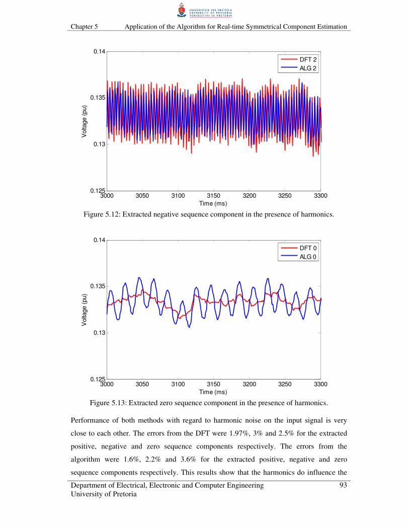
Chapter 5 Application of the Algorithm for Real-time Symmetrical Component Estimation
Department of Electrical, Electronic and Computer Engineering
University of Pretoria
93
3000 3050 3100 3150 3200 3250 33000.125
0.13
0.135
0.14
Time (ms)
Volta
ge (
pu)
DFT 2
ALG 2
Figure 5.12: Extracted negative sequence component in the presence of harmonics.
3000 3050 3100 3150 3200 3250 33000.125
0.13
0.135
0.14
Time (ms)
Volta
ge (
pu)
DFT 0
ALG 0
Figure 5.13: Extracted zero sequence component in the presence of harmonics.
Performance of both methods with regard to harmonic noise on the input signal is very
close to each other. The errors from the DFT were 1.97%, 3% and 2.5% for the extracted
positive, negative and zero sequence components respectively. The errors from the
algorithm were 1.6%, 2.2% and 3.6% for the extracted positive, negative and zero
sequence components respectively. This results show that the harmonics do influence the

Chapter 5 Application of the Algorithm for Real-time Symmetrical Component Estimation
Department of Electrical, Electronic and Computer Engineering
University of Pretoria
94
accuracy of both methods. The algorithm offers improved accuracy for the positive and
negative sequence component.
5.3 APPLICATION TO FIELD DATA
In this section the performance of the proposed method is tested against field data. Two
different cases of transmission system fault types are studied. The DFT is used to
benchmark the algorithm for the application to field data. IEEE comtrade files that were
played back through the Transplay function of the Omicron 56 were used to inject the fault
data into the PC Matlab Operator through the d-Space analog-to-digital converter.
5.3.1 Case 1: 400kV Transmission Line Single Phase Fault
Figure 5.14 shows a single line-ground fault on a 400kV transmission line. Line inspection
revealed that the source of the fault was a bird. The sampling frequency was 2.5kHz (50
sample/cycle). The pre and post fault voltages are shown in Figure 5.14. The fault occurred
on phase B at approximately 1.3s. The results indicate that the algorithm is able to track the
symmetrical components of the voltage to within 1% of that of the DFT on the positive
sequence. The response of the algorithm, at the inception of the fault, is 11.82ms for the
positive sequence component, and 14ms for the negative and zero sequence components.
This is faster than the response of the DFT. Figure 5.15 to Figure 5.17 show the respective
positive, negative and zero sequence components for the algorithm and for the DFT. For
the negative and zero sequences the proposed method is still quicker than the DFT at the
inception of the fault.

Chapter 5 Application of the Algorithm for Real-time Symmetrical Component Estimation
Department of Electrical, Electronic and Computer Engineering
University of Pretoria
95
1000 1200 1400 1600 1800 2000 2200 2400
-1
-0.8
-0.6
-0.4
-0.2
0
0.2
0.4
0.6
0.8
1
Time (ms)
Volta
ge (
pu)
Va
Vb
Vc
Figure 5.14: Three-phase voltage at fault instant for Case 1.
1100 1200 1300 1400 1500 1600 1700
-1
-0.8
-0.6
-0.4
-0.2
0
0.2
0.4
0.6
0.8
1
Time (ms)
Volta
ge (
pu)
DFT 1
ALG 1
Vb
Figure 5.15: Positive sequence component extraction for Case 1.
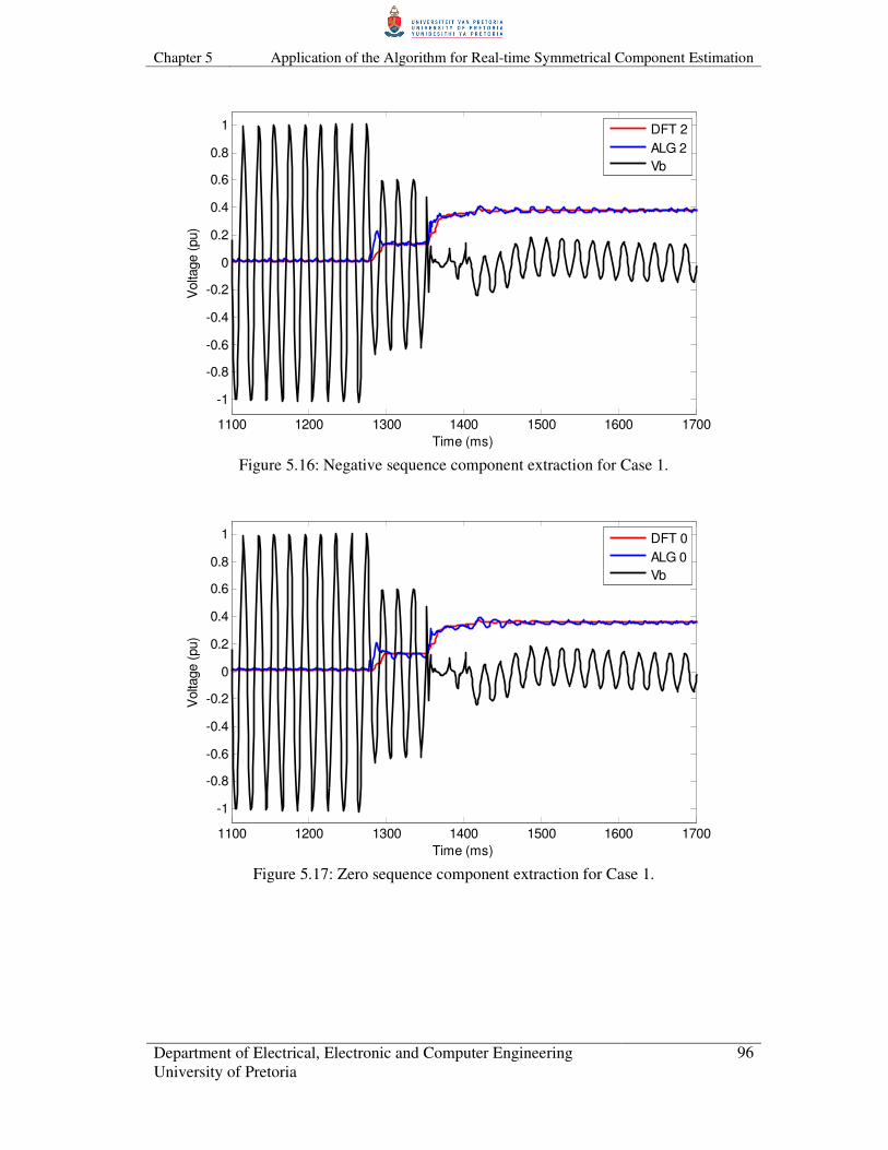
Chapter 5 Application of the Algorithm for Real-time Symmetrical Component Estimation
Department of Electrical, Electronic and Computer Engineering
University of Pretoria
96
1100 1200 1300 1400 1500 1600 1700
-1
-0.8
-0.6
-0.4
-0.2
0
0.2
0.4
0.6
0.8
1
Time (ms)
Volta
ge (
pu)
DFT 2
ALG 2
Vb
Figure 5.16: Negative sequence component extraction for Case 1.
1100 1200 1300 1400 1500 1600 1700
-1
-0.8
-0.6
-0.4
-0.2
0
0.2
0.4
0.6
0.8
1
Time (ms)
Volta
ge (
pu)
DFT 0
ALG 0
Vb
Figure 5.17: Zero sequence component extraction for Case 1.

Chapter 5 Application of the Algorithm for Real-time Symmetrical Component Estimation
Department of Electrical, Electronic and Computer Engineering
University of Pretoria
97
5.3.2 Case 2: 275kV Transmission Line Single Phase Fault
Figure 5.18 shows a single line-ground fault on a 275kV transmission line. Line inspection
revealed that the source of the fault was a fire. The sampling frequency was 2.5kHz (50
sample/cycle). The pre and post fault voltages are shown in Figure 5.18. The fault occurred
in Phase B at approximately 1.24s. The results indicate that the algorithm is able to track
the symmetrical components of the voltage to within 1% of that of the DFT on the positive
sequence. The algorithm has a margin of 3% in relation to that of the DFT on the negative
and zero sequence components. The response of the algorithm, at the inception of the fault,
is 10ms for the positive sequence component, and 6ms for the negative and zero sequence
components. This is quicker than the response of the DFT.
Figure 5.19 to Figure 5.21 show the respective positive, negative and zero sequence
components for the proposed method and the DFT. This shows that for the positive
sequence the algorithm is very fast and accurate in comparison to that of the DFT. For the
negative and zero sequences, the algorithm method is still faster than the DFT at the
inception of the fault.
1000 1200 1400 1600 1800 2000 2200 2400
-1
-0.8
-0.6
-0.4
-0.2
0
0.2
0.4
0.6
0.8
1
Time (ms)
Volta
ge (
pu)
Va
Vb
Vc
Figure 5.18: Three-phase voltage at the fault instant for Case 2.

Chapter 5 Application of the Algorithm for Real-time Symmetrical Component Estimation
Department of Electrical, Electronic and Computer Engineering
University of Pretoria
98
1100 1200 1300 1400 1500 1600 1700
-1
-0.8
-0.6
-0.4
-0.2
0
0.2
0.4
0.6
0.8
1
Time (ms)
Volta
ge (
pu)
DFT 1
ALG 1
Vb
Figure 5.19: Positive sequence component extraction for Case 2.
1100 1200 1300 1400 1500 1600 1700
-1
-0.8
-0.6
-0.4
-0.2
0
0.2
0.4
0.6
0.8
1
Time (ms)
Volta
ge (
pu)
DFT 2
ALG 2
Vb
Figure 5.20: Negative sequence component extraction for Case 2.
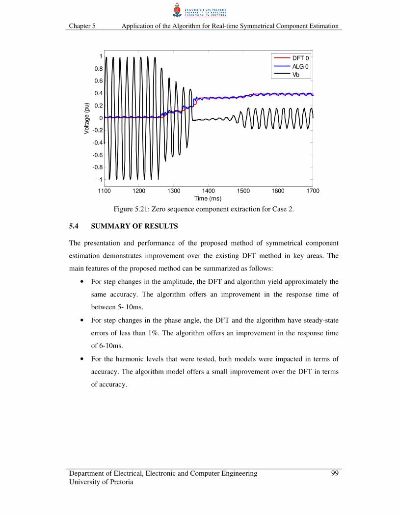
Chapter 5 Application of the Algorithm for Real-time Symmetrical Component Estimation
Department of Electrical, Electronic and Computer Engineering
University of Pretoria
99
1100 1200 1300 1400 1500 1600 1700
-1
-0.8
-0.6
-0.4
-0.2
0
0.2
0.4
0.6
0.8
1
Time (ms)
Volta
ge (
pu)
DFT 0
ALG 0
Vb
Figure 5.21: Zero sequence component extraction for Case 2.
5.4 SUMMARY OF RESULTS
The presentation and performance of the proposed method of symmetrical component
estimation demonstrates improvement over the existing DFT method in key areas. The
main features of the proposed method can be summarized as follows:
• For step changes in the amplitude, the DFT and algorithm yield approximately the
same accuracy. The algorithm offers an improvement in the response time of
between 5- 10ms.
• For step changes in the phase angle, the DFT and the algorithm have steady-state
errors of less than 1%. The algorithm offers an improvement in the response time
of 6-10ms.
• For the harmonic levels that were tested, both models were impacted in terms of
accuracy. The algorithm model offers a small improvement over the DFT in terms
of accuracy.

Chapter 5 Application of the Algorithm for Real-time Symmetrical Component Estimation
Department of Electrical, Electronic and Computer Engineering
University of Pretoria
100
5.5 CONCLUDING REMARKS
In this chapter a model was tested to determine symmetrical components in real-time
through the injection of voltages. The method converts a three-phase signal into a time-
domain phasor. The standard symmetrical component matrix is used to convert the three
phasors into positive, negative and zero sequence components in real time. The system was
tested by injecting actual voltages into an analog-to-digital processor for real-time
processing. Theoretical calculations were used to benchmark and compare the response of
the algorithm and the DFT, as well as to compare the results of this chapter to the results
obtained by means of experiments. The effects of changes in amplitude, phase and the
influence of harmonics were tested. The results that were obtained confirm the
improvement in performance over the DFT model. Field data in the form of two phase-to-
earth faults on transmission lines was injected through IEEE comtrade files to compare the
algorithm to the DFT. The algorithm proved to be stable under the fault conditions and
yielded improved response times at the inception of the faults.

Department of Electrical, Electronic and Computer Engineering
University of Pretoria
101
CHAPTER 6
CONCLUSION
6.1 INTRODUCTION
A core algorithm developed with the intention of overcoming the inherent shortcomings of
the standard signal processing tools such as DFT and linear adaptive filtering, was applied
to power system applications. This was done to demonstrate the power of the core
algorithm as well as to present new methods to use in power systems. The range of its
applications is not limited to those discussed in this dissertation. The results obtained
through the research done in this dissertation are summarized in this chapter. Finally,
opportunities for future research work are proposed.
6.2 SUMMARY OF RESULTS
The algorithm’s parameter settings were tested and optimized. The results indicated that
the algorithm can be optimized for accurate and rapid response.
The three applications that were tested include:
• controlling an automatic voltage regulator on a synchronous generator;
• voltage dip mitigation; and
• real-time symmetrical component estimation.
6.2.1 Control of an Automatic Voltage Regulator on a Synchronous Generator
The algorithm was compared to a diode bridge rectifier as a method to track the terminal
voltage of a synchronous generator. The resultant voltage was then used as the input to the
automatic voltage regulator that controls the terminal voltage of the synchronous generator.
It was found that there is no significant difference in overall responses of the synchronous
generator for the two methods. Both methods displayed stability and adequately fast
performance to sufficiently control the generator terminal voltage. A comparison between
the field voltages of both methods shows a very good relation between the two methods

Chapter 6 Conclusion
Department of Electrical, Electronic and Computer Engineering
University of Pretoria
102
with almost identical characteristics. This was because the performance of the synchronous
generator is governed by the high synchronous reactance Xd. Advances in High
Temperature superconductors are enabling a new class of synchronous rotating machines
that can be categorized as “Super Machines”. These are machines with a low synchronous
reactance (typically Xd = 0.5 per unit), which assures dynamic stability within its MVA
(Mega Voltage-Amperes) rating and provides better voltage regulation than a conventional
machine.
With this new emerging technology the effect of Xd can be minimized and faster tracking
methods can be utilized more effectively through faster excitation response of the
synchronous condenser.
6.2.2 Voltage Dip Mitigation
The algorithm was used in two voltage dip mitigation studies. The first study investigated
the control of a synchronous condenser for dip mitigation on a distribution system. The
second study investigated the switching of a capacitor for dip mitigation on a PC.
For the first study, the simulation results showed that the algorithm’s method of sensing
the magnitude of the voltage, and using it as the input into the AVR to control the field
voltage, is accurate enough to provide the synchronous condenser control with rapid
voltage magnitude feedback. The algorithm displayed stability and quick performance to
sufficiently control the condenser, not only under steady state conditions, but under fault
conditions as well, and thus the network voltage.
It was also shown that the algorithm detects the voltage dip quick enough to switch the DC
storage device into the circuit before an interruption in the PC’s operation is experienced.
This has use for tracking decaying “DC” bus voltages.
6.2.3 Real time symmetrical component estimation
The algorithm was used in a model that can estimate symmetrical components in real time.
The results from the algorithm model were compared to that of a DFT model. The results
showed a good correlation between the simulated and practical results. This showed that

Chapter 6 Conclusion
Department of Electrical, Electronic and Computer Engineering
University of Pretoria
103
the algorithm model responds faster than the DFT and that the algorithm is also more
accurate than the DFT in key areas of certain case studies.
6.3 FUTURE WORK
The results in this dissertation have shown that the algorithm can be used in a wide range
of applications in the power system. Further work can be carried out in the following areas:
• Field-testing of a synchronous generator – Much of the work presented in this
dissertation on synchronous generator excitation control is based on simulations.
Further research can be conducted to field test the responses that were simulated.
• Parameter optimization – Further research can be carried out to optimize the
algorithm for specific applications to obtain the best results in terms f accuracy and
speed.
• Setting procedures – Develop a procedure for the setting of the algorithm
parameters for each of the three sinusoidal parameters, magnitude, phase and
frequency. Currently there is no proven method of determining the algorithm
parameters.
• LFC control – Use the algorithm to load frequency control on a synchronous
generator through fast frequency tracking.
• Network fault detection – Fast detection of network faults through symmetrical
component estimation and comparing response times to in-service protection
relays.
With the further development of the algorithm’s setting parameters, more applications can
be investigated and the consequent further development of the current applications is
proposed.

References
Department of Electrical, Electronic and Computer Engineering
University of Pretoria
104
REFERENCES
[1] A. K. Ziarani, “Extractions on non-stationary sinusoids”, A thesis in conformity
with the requirements for the degree of Doctor of Philosophy, University of
Toronto, 2002.
[2] J. Li, X. Xie, J. Xiao, J. WU, “The framework and algorithm of a new phasor
measurement unit”, IEEE International Conference on Electric Utility
Deregulation, Restructuring and Power Technologies, Hong-Kong, 5-8 April, 2004
pp. 826 - 831.
[3] M. M. Begovic, P. M. Djuric, S. Dunlap, A. G. Phadke, “Frequency tracking in
power networks in the presence of harmonics”, IEEE Transactions on Power
Delivery, Vol. 8, No. 2, pp. 480 – 486, April 1993.
[4] T. K. Abdel-Galil, E. F. El-Saadany, M. M. A. Salama, “Online Tracking of
Voltage Flicker Utilizing Energy Operator and Hilbert Transform”, IEEE
Transactions on Power Delivery, Vol. 19, No. 2, pp. 861 – 867, April 2004.
[5] M. I. Marei, T. K. Abdel-Galil, E. F. El-Saadany, M. M. A. Salama, “Hilbert
Transform Based Control Algorithm of the DG Interface for Voltage Flicker
Mitigation”, IEEE Transactions on Power Delivery, Vol. 20, No. 2, pp. 1129 –
1133, April 2005.
[6] I. Kamwa and R. Grondin, “Fast Adaptive Schemes for Tracking Voltage Phasor
and Local Frequency in Power Transmission and Distribution Systems”, IEEE
Transactions on Power Delivery, Vol. 7, No. 2, pp. 789 – 795, April 1992.
[7] R. A. de Macedo, D. da Silva Filho, D. V. Couty, A. A. de Franca Mendes
Carneiro, “An Evolutionary Optimization Approach to Track Voltage and Current
Harmonics in Electrical Power Systems”, IEEE Power Engineering Society
Meeting, pp. 1250 – 1255, 13-17 July 2003.
[8] S. Chan and C. Lei, “Study on Building Digital Power System Simulator –
Matlab/Simulink based Transient Analysis and Simulation of Synchronous
Generators”, Power System Technology, PowerCon Proceedings, Vol. 3, pp. 1558 -
1562, October 2002.
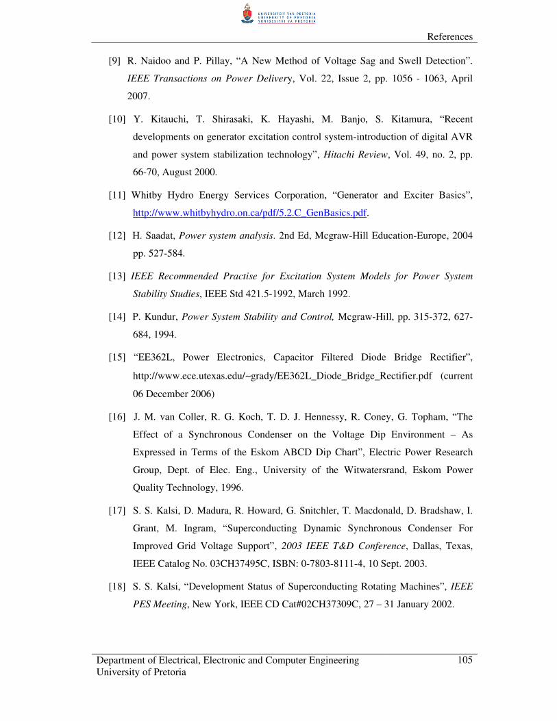
References
Department of Electrical, Electronic and Computer Engineering
University of Pretoria
105
[9] R. Naidoo and P. Pillay, “A New Method of Voltage Sag and Swell Detection”.
IEEE Transactions on Power Delivery, Vol. 22, Issue 2, pp. 1056 - 1063, April
2007.
[10] Y. Kitauchi, T. Shirasaki, K. Hayashi, M. Banjo, S. Kitamura, “Recent
developments on generator excitation control system-introduction of digital AVR
and power system stabilization technology”, Hitachi Review, Vol. 49, no. 2, pp.
66-70, August 2000.
[11] Whitby Hydro Energy Services Corporation, “Generator and Exciter Basics”,
http://www.whitbyhydro.on.ca/pdf/5.2.C_GenBasics.pdf.
[12] H. Saadat, Power system analysis. 2nd Ed, Mcgraw-Hill Education-Europe, 2004
pp. 527-584.
[13] IEEE Recommended Practise for Excitation System Models for Power System
Stability Studies, IEEE Std 421.5-1992, March 1992.
[14] P. Kundur, Power System Stability and Control, Mcgraw-Hill, pp. 315-372, 627-
684, 1994.
[15] “EE362L, Power Electronics, Capacitor Filtered Diode Bridge Rectifier”,
http://www.ece.utexas.edu/∼grady/EE362L_Diode_Bridge_Rectifier.pdf (current
06 December 2006)
[16] J. M. van Coller, R. G. Koch, T. D. J. Hennessy, R. Coney, G. Topham, “The
Effect of a Synchronous Condenser on the Voltage Dip Environment – As
Expressed in Terms of the Eskom ABCD Dip Chart”, Electric Power Research
Group, Dept. of Elec. Eng., University of the Witwatersrand, Eskom Power
Quality Technology, 1996.
[17] S. S. Kalsi, D. Madura, R. Howard, G. Snitchler, T. Macdonald, D. Bradshaw, I.
Grant, M. Ingram, “Superconducting Dynamic Synchronous Condenser For
Improved Grid Voltage Support”, 2003 IEEE T&D Conference, Dallas, Texas,
IEEE Catalog No. 03CH37495C, ISBN: 0-7803-8111-4, 10 Sept. 2003.
[18] S. S. Kalsi, “Development Status of Superconducting Rotating Machines”, IEEE
PES Meeting, New York, IEEE CD Cat#02CH37309C, 27 – 31 January 2002.

References
Department of Electrical, Electronic and Computer Engineering
University of Pretoria
106
[19] M. H. J. Bollen, Equipment Behavior, Understanding Power Quality Problems:
Voltage Sags and Interruptions, IEEE Press New York, Gothenburg, October
1999.
[20] R. M. Naidoo, “A nonlinear adaptive filter for improved operation and protection
of power systems”, A thesis in conformity with the requirements for the degree of
Doctorate of Philosophy, University of Cape Town, 2008.

List of Figures
Department of Electrical, Electronic and Computer Engineering
University of Pretoria
107
LIST OF FIGURES
Figure 2.1: Implementation of the algorithm as a Simulink model [1]. ............................. 15
Figure 2.2: Terminal voltage magnitude tracked by the algorithm. ................................... 16
Figure 2.3: Simulink model used for the testing of the algorithm’s parameter settings. ..... 17
Figure 2.4: Algorithm amplitude tracking results for tests 1 to 3. ...................................... 18
Figure 2.5: Algorithm amplitude tracking results for tests 4 to 6. ...................................... 19
Figure 2.6: Algorithm amplitude tracking results for tests 7 to 9. ...................................... 20
Figure 2.7: Forward and reverse phase shifts. ................................................................... 21
Figure 2.8: Algorithm phase tracking for 60° forward step change with normal parameters.
........................................................................................................................................ 22
Figure 2.9: Phase tracking for 60° backward step change with normal parameters. ........... 22
Figure 2.10: Phase tracking for 60° forward step change with optimized parameters. ....... 23
Figure 2.11: Phase tracking for 60° backward step change with optimized parameters. .... 23
Figure 2.12: Frequency tracking for a 2Hz increase. ......................................................... 24
Figure 2.13: Frequency tracking for a 2Hz decrease. ........................................................ 25
Figure 3.1: Schematic diagram of LFC and AVR control loops [12]. ................................ 30
Figure 3.2: Block diagram for a synchronous machine excitation control system [12]. ..... 31
Figure 3.3: Typical arrangement of a simple AVR [12]. ................................................... 32
Figure 3.4: Single-phase diode bridge rectifier with capacitor filter [15]........................... 34
Figure 3.5: AC and DC voltage waveforms with the DC load resistor and no capacitor [15].
........................................................................................................................................ 34
Figure 3.6: Impact of C on the load voltage [15]. ............................................................. 34
Figure 3.7: DC-side current Idc for two different load levels [15]. ..................................... 35
Figure 3.8: AC-side current Iac [15]. ................................................................................. 36
Figure 3.9: Approximation of the waveform used for ripple calculation formula [15]. ...... 37
Figure 3.10: Diode bridge rectifier used in the research simulations. ................................ 38
Figure 3.11: Diode bridge connections. ............................................................................ 38
Figure 3.12: Terminal voltage vs. diode bridge rectifier output without filter circuit. ........ 39
Figure 3.13: Terminal voltage vs. diode bridge rectifier output with filter circuit. ............. 39
Figure 3.14: Model for the direct comparison between the diode bridge rectifier and the
algorithm. ........................................................................................................................ 40
Figure 3.15: Algorithm test set 1 results. .......................................................................... 43
Figure 3.16: Algorithm test set 2 results. .......................................................................... 43
Figure 3.17: Diode bridge rectifier test set 1 results. ......................................................... 44
Figure 3.18: Diode bridge rectifier test set 2 results. ......................................................... 44
Figure 3.19: Diode bridge rectifier compared to the algorithm. ......................................... 45
Figure 3.20: Diode bridge rectifier compared to the algorithm. ......................................... 45
Figure 3.21: Closed-loop model using the algorithm. ....................................................... 46
Figure 3.22: Closed-loop model using the diode bridge rectifier. ...................................... 47
Figure 3.23: IEEE Type ST1- potential source control rectifier [14]. ................................ 47
Figure 3.24: Actual stator voltage measured for a 10% step-change in magnitude. ........... 49
Figure 3.25: Stator voltage measured compared to a simulated response. ......................... 50
Figure 3.26: Stator voltage measured compared to a simulated response. ......................... 51
Figure 3.28: Algorithm tracking the resultant terminal voltage for Test 8. ........................ 54
Figure 3.29: Algorithm tracking the resultant terminal voltage for Test 4. ........................ 54
Figure 3.30: Frequency response using Algorithm 2 for Test 4 and Test 8. ....................... 55
Figure 3.31: Excitation voltage response using Algorithm 2 for Test 4 and Test 8. ........... 55
Figure 3.32: DBR tracking the resultant terminal voltage for Test 8. ................................ 56
Figure 3.33: DBR tracking the resultant terminal voltage for Test 4. ................................ 56

List of Figures
Department of Electrical, Electronic and Computer Engineering
University of Pretoria
108
Figure 3.34: Frequency response using the DBR for Test 4 and Test 8. ............................ 57
Figure 3.35: Excitation voltage response using the DBR for Test 4 and Test 8. ................ 57
Figure 3.36: Algorithm-tracked voltages for Test 1 to Test 8 using Algorithm 2. .............. 58
Figure 3.37: Algorithm-tracked voltages for Test 1 to Test 8 using DBR. ......................... 58
Figure 4.1. Typical waveform of a voltage dip caused by remote fault clearing. ............... 62
Figure 4.2: Simulated network with the synchronous condenser. ...................................... 65
Figure 4.3: Synchronous condenser field voltage.............................................................. 66
Figure 4.4: Synchronous condenser rotor speed. ............................................................... 66
Figure 4.5: Synchronous condenser reactive power delivery............................................. 67
Figure 4.6: Voltage waveforms for additional loading. ..................................................... 68
Figure 4.7: 11kV voltage profiles for a 400kV fault. ........................................................ 69
Figure 4.8: 11kV voltage profiles for a 132kV fault. ........................................................ 70
Figure 4.9: 11kV Voltage Profiles for a 11kV Fault. ........................................................ 70
Figure 4.10: Experimental setup for dips on a PC. ............................................................ 74
Figure 4.11: CBEMA curve vs. PC power supply. ............................................................ 75
Figure 4.12: Test 1: 30% 2s dip. ....................................................................................... 76
Figure 4.13: Test 1: 50% 32ms dip. .................................................................................. 76
Figure 4.14: Test 3: 30% 4s dip. ....................................................................................... 77
Figure 4.15: Test 3: 50% 1.5s dip. .................................................................................... 78
Figure 4.16: Test 3: 70% 1.4s dip. .................................................................................... 78
Figure 4.17: Test 3: capacitor discharge voltages. ............................................................ 79
Figure 5.1: Zero, positive and negative sequence components. ......................................... 82
Figure 5.2: Experimental setup. ........................................................................................ 84
Figure 5.3: Input waveform .............................................................................................. 85
Figure 5.4: Resultant sequence components for a 0.6pu step in Phase B. .......................... 86
Figure 5.5: Resultant sequence components for a 0.6pu step increase in Phase B. ............ 86
Figure 5.6: Resultant sequence components for a ramp up and down in Phase B. ............. 88
Figure 5.7: Resultant sequence components for a 60° phase change down in Phase B. ..... 89
Figure 5.8: Resultant sequence components for a 60° phase change up in Phase B. .......... 90
Figure 5.9: Resultant sequence components for a ramp in phase angle of Phase B. ........... 91
Figure 5.10: Input signal in the presence of harmonics. .................................................... 92
Figure 5.11: Extracted positive sequence component in the presence of harmonics. ......... 92
Figure 5.12: Extracted negative sequence component in the presence of harmonics.......... 93
Figure 5.13: Extracted zero sequence component in the presence of harmonics. ............... 93
Figure 5.14: Three-phase voltage at fault instant for Case 1. ............................................ 95
Figure 5.15: Positive sequence component extraction for Case 1. ..................................... 95
Figure 5.16: Negative sequence component extraction for Case 1. ................................... 96
Figure 5.17: Zero sequence component extraction for Case 1. .......................................... 96
Figure 5.18: Three-phase voltage at the fault instant for Case 2. ....................................... 97
Figure 5.19: Positive sequence component extraction for Case 2. ..................................... 98
Figure 5.20: Negative sequence component extraction for Case 2. ................................... 98
Figure 5.21: Zero sequence component extraction for Case 2. .......................................... 99

List of Tables
Department of Electrical, Electronic and Computer Engineering
University of Pretoria
109
LIST OF TABLES
Table 2.1: The proposed algorithm’s parameter settings. .................................................. 17
Table 3.1: Filter parameters. ............................................................................................. 38
Table 3.2: Algorithm test set 1 results. ............................................................................. 41
Table 3.3: Diode bridge rectifier test set 1 results. ............................................................ 41
Table 3.4: Algorithm test set 2 results. ............................................................................. 42
Table 3.5: Diode bridge rectifier test set 2 results. ............................................................ 42
Table 3.6: Synchronous machine parameters. ................................................................... 48
Table 3.7: Assumed synchronous machine parameters. .................................................... 49
Table 3.8: Automatic voltage regulator setting parameters. .............................................. 50
Table 3.9: Loading conditions for the eight studies........................................................... 52
Table 3.10: Response times of the terminal voltage synchronous generator. ..................... 53
Table 4.1: PC power supply operation response times. ..................................................... 75
Table 5.1: Summary of results showing the effects of a step change in magnitude. ........... 87
Table 5.2: Summary of results showing the effects of a change in the phase angle. .......... 89