a mems based coulter counter for cell sizing
TRANSCRIPT
A MEMS BASED COULTER COUNTER FOR CELL
SIZING
A Thesis presented to the Faculty of the Graduate School University of Missouri-Columbia
In Partial Fulfillment of the Requirements for the Degree
Master of Science
By
MADHURI KORAMPALLY
Dr. Mahmoud Almasri, Thesis Supervisor
DECEMBER 2007

The undersigned, appointed by the dean of the Graduate School, have examined the
thesis entitled
A MEMS BASED COULTER COUNTER FOR CELL SIZING
presented by Madhuri Korampally,
a candidate for the degree of Master of Science,
and hereby certify that, in their opinion, it is worthy of acceptance.
Dr. Mahmoud Almasri
Dr. Naz Islam
Dr. John Critser

ii
ACKNOWLEDGEMENTS
I am greatly indebted to my advisor Dr. Mahmoud Almasri for his willingness to
accept me into his research group and his constant guidance, encouragement and help
during my hard times. His mentorship and help had a great impact on my life and made
my past years a very special time. I am grateful to Dr. John Critser not only for his
immense help and valuable guidance but also for the financial support he extended
without which this thesis would not have been possible. I would like to sincerely thank
Dr. Shubhra Gangopadhyay and her students for letting me use the lab facility. I owe a
great deal of appreciation for their patience, time and valuable support.
I would like to extend my thanks to my fellow graduate students Yiren Wang and
Qi Cheng for their help and support during my research. I would specially like to thank
James Benson for his help and support during the experimentation.
I take this opportunity to thank my committee members Dr. Mahmoud Almasri, Dr.
John Critser, Dr. Naz Islam for their time and consideration in reading my thesis and for
their help in defining and completing my thesis.
I would also like to thank Shirley Holdmeier and Susan Wayt for always lending a
helpful hand. Finally I take this opportunity to thank my friends and family for their love
and support. I specially want to thank my brother Venu, my husband Mayur and my
parents for their encouragement, love and support throughout my life.

iii
TABLE OF CONTENTS
ACKNOWLEDGEMENTS................................................................................................ II LIST OF FIGURES…………………………………………………………………….....V LIST OF TABLES……………………………………………………………………...VIII ABSTRACT………………………………………………………………………….. …IX
CHAPTER 1: INTRODUCTION .................................................................................. 1
1.1 Evolution of MEMS........................................................................................ 1 1.1.1 BioMEMS...................................................................................................... 2
1.2 Cell Based Microsystems................................................................................ 3 1.2.1 Cell Counting - Traditional Methods............................................................. 4
1.3 Coulter Counter Method of Counting Cells.................................................... 6 1.3.1 Classical Coulter Counter .............................................................................. 6 1.3.2 Miniaturization of Coulter Counter ............................................................... 7
1.4 Overview of Existing Coulter Counter Devices ............................................. 8 1.5 Flow Cytometry ............................................................................................ 13
1.5.1 Conventional Flow cytometers- Hydrodynamic Focusing .......................... 14 1.5.2 Drawbacks of Hydrodynamic Focusing ...................................................... 15
1.6 Desirable Features of an Ideal Cell Counter ................................................. 17 1.7 Main Objectives of the Thesis ...................................................................... 17
CHAPTER 2: THEORETICAL ANALYSIS .............................................................. 19
2.1 Mixing........................................................................................................... 19 2.2 Electrokinetics .............................................................................................. 21
2.2.1 Comparison of Behavior of Neutral and Charged Bodies in Uniform and Non-Uniform Electric Fields.................................................. 23
2.2.2 Dielectrophoresis ......................................................................................... 24 2.3 Experimental Setup....................................................................................... 28
2.3.1 Setup for Measurement of Change in Resistance ........................................ 28 2.3.2 Setup for Dielectrophoretic Focusing .......................................................... 30
CHAPTER 3: DESIGN AND MODELLING ............................................................. 31
3.1 Overview of the Design ................................................................................ 31 3.1.1 Mixing Region ............................................................................................. 32 3.1.2 Focusing Region .......................................................................................... 33 3.1.3 Sensing or Measuring Region...................................................................... 34
3.2 Design-1........................................................................................................ 35 3.3 Design-2........................................................................................................ 38
3.3.1 Description of Design-2............................................................................... 38 3.3.2 Modeling of Design-2.................................................................................. 41
CHAPTER 4: FABRICATION AND PACKAGING ................................................. 46
iv
4.1 Materials Used in the Fabrication ................................................................. 46 4.1.1 Metals........................................................................................................... 46 4.1.2 SU8 as the Channel Material ....................................................................... 48 4.1.3 Polydimethylsiloxane (PDMS) .................................................................... 50
4.2 Fabrication .................................................................................................... 51 4.2.1 Fabrication Steps of Design-1...................................................................... 51 4.2.2 Fabrication Steps of Design-2...................................................................... 57
CHAPTER 5: RESULTS AND DISCUSSION........................................................... 61
5.1 Approach to Device Testing ......................................................................... 61 5.2 Fluid Flow in the Channel............................................................................. 62
5.2.1 Glass Cover to Seal the Channel.................................................................. 62 5.2.2 PDMS to Seal the Channel .......................................................................... 63
5.3 Mixing of Two Fluids in the Channel........................................................... 65 CHAPTER 6: CONCLUSION AND FUTURE WORK ............................................. 67
6.1 Micro Devices for Cell Sensing and Analysis .............................................. 67 6.2 Future Work .................................................................................................. 68
6.2.1 The Cell Types Primarily Being Considered............................................... 68 REFERENCES ................................................................................................................. 70 APPENDIX………………………………………………………………………………76

v
LIST OF FIGURES
Figure 1.1. Integration of micro/nano scale systems with biomedical sciences [5]. .......... 2 Figure 1.2 Schematic diagram showing the working principle of the coulter counter. ..... 7 Figure 1.3 Micro coulter particle counter by Larsen et al [31]. ......................................... 9 Figure 1.4 Hydrodynamic focusing mechanism by Larsen et al, 1) sample flow, 2) sheathed electrolyte flow, 3) non-conducting spacer liquid. .............................................. 9 Figure 1.5 Micro coulter counter (Koch et al) [32]. ........................................................ 10 Figure 1.6 Schematics of the coulter counter (M.Koch et al) showing the silicon trench and the measuring electrodes. ................................................................................ 11 Figure 1.7 Schematic view of the micro channel by Gawad et.al showing the particle passing over three electrodes, differential impedance is measured as Zac-Zbc [33]. ................................................................................................................................... 11 Figure 1.8 a) Micro-fabricated chip with the PDMS cover and fluidic connectors b) chip on chip configuration. S.Gawad et al.................................................................... 12 Figure 1.9 Integrated coulter counter by Kohl et al [34]. ................................................. 12 Figure 1.10 Schematic representation of a conventional flow cytometer........................ 14 Figure 1.11 Microscope images showing the effect of hydrodynamic focusing, Qf = 10µl/min............................................................................................................................ 15 Figure 2.1 Comparison of the behavior of charged and neutral bodies when subjected to uniform and non-uniform electric fields....................................................... 23 Figure 2.2 Schematic diagram showing the positive and negative dielectrophoretic forces on particles subjected to non-uniform electric fields. ............................................ 25 Figure 2.3 Experimental setup for the measurement of change in resistance.................. 29 Figure 3.1 Image showing the three regions in the device a) mixing region, b) focusing region, c) measuring or sensing region.......................................................... 32 Figure 3.2 Images showing the masks used in the fabrication. ........................................ 37 Figure 3.3 Schematic diagram of design-2 showing the different components................ 38

vi
Figure 3.4 Pictures of all the masks for the fabrication of the device using design-2. ..... 39 Figure 3.5 Schematic of the layout for design-2............................................................... 40 Figure 3.6 A part of the rectangular electrode array forming the micro-fluidic channel. ............................................................................................................................. 40 Figure 3.7 Result obtained with: length of electrodes= 20µm; gap between adjacent electrodes= 5µm; V=15V.................................................................................................. 41 Figure 3.8 Result obtained with: length of electrodes= 10µm; gap between adjacent electrodes= 10µm; V=15V................................................................................................ 42 Figure 3.9 Electric field distribution with: width of electrodes=40µm; gap between adjacent electrodes=10µm; width of channel=100µm; height of the channel=50µm....... 43 Figure 3.10 Electric field distribution with: width of electrodes=60µm; gap between adjacent electrodes=10µm; width of channel=40µm; height of the channel=40µm......... 44 Figure 4.1 Sputtering system ............................................................................................ 47 Figure 4.2 Image of the Electroplating setup.................................................................... 48 Figure 4.3 Illustration of the procedure for fabricating PDMS stamps. ........................... 51 Figure 4.4 Fabrication steps of the device using Design-1............................................... 52 Figure 4.5 Picture of the complete fabricated device with the PDMS cover and fluidic connectors. ........................................................................................................................ 54 Figure 4.6 Mask for Patterning the PCB package............................................................. 54 Figure 4.7 Microscopic image of the device showing the SU8 channel with the focusing electrodes, measuring electrodes, inlet and outlet ports............................... 55 Figure 4.8 Magnified images of the channel showing the two different electrode configurations with a serpentine shaped mixing channel. ................................................ 55 Figure 4.9 Image showing the device with straight mixing region................................... 56 Figure 4.10 Image of the device with wire bonding and packaging................................. 56 Figure 4.11 Pictures of all the masks for the fabrication of the device using Design-2 ... 60 Figure 5.1Setup for fluidic testing .................................................................................... 62

vii
Figure 5.2 Microscopic image showing the leak in the mid-section of the channel........ 63 Figure 5.3 Fluid flow in a device with PDMS sheet sealing the channel ........................ 65 Figure 5.4 No mixing seen at high flow rates................................................................... 66 Figure 5.5 Mixing at different flow rates......................................................................... 66

viii
LIST OF TABLES
Table 3-1shows the various configurations of electrodes studied using Silvaco, V=15V, Width of the channel=40 µm and Thickness of electrodes = 200nm. ................ 43 Table 3-2 shows the different electrode configurations studied using CST Microwave Studio..................................................................................................... 45

ix
ABSTRACT
Detection and classification of cells forms an important aspect of medical research
in diagnosing diseases and finding remedies at the cellular level. Miniaturized cell
detecting devices are desirable not only for on site biomedical analysis but also for in situ
monitoring of cell dynamics.
This research presents the design and fabrication of a MEMS based Coulter counter for
monitoring cellular volumetric changes after an exposure to various media. The device is based
on three important phenomena: 1) Passive mixing of the reagents, 2) Dielectrophoretic focusing
of the cells and 3) Electrical impedance based sensing mechanism.
This device improves upon existing macro-scale Coulter counter technology by allowing
extremely small sample sizes (101 compared to 105 cells per experiment), an extremely short time
frame from the exposure to reactant media to the initial measurement, serial time series
measurements of a single cell, and optical microscopic monitoring of the experiment. Finally, the
design of this device will allow for the manufacture of cell specific channel diameters in order to
maximize measurement precision for each cell type.

1
CHAPTER 1: INTRODUCTION
1.1 Evolution of MEMS
New developments in the Integrated Circuit (IC) technology and materials led to
the production of micro-devices incorporating both mechanical and electronic
functionality for sensing actuation and control [1,2]. These devices qualify as
Microelectromechanical Systems (MEMS): systems which combine mechanical and
electrical components and are fabricated using semiconductor fabrication techniques.
These systems include tiny mechanical devices that are built onto semiconductor chips
whose dimensions are in the range of a few micrometers. The advantages of these
systems are low cost, low power consumption, miniaturization, integration and high
performance. MEMS technology has been rapidly growing since the last two decades and
now they are not just restricted to electrical and mechanical systems but are widely being
used in physics, chemistry, biology, medicine, optics and aerospace. MEMS technology
is thus diverse and includes many sub-fields such as Optical MEMS, RF MEMS,
BioMEMS etc [3].

2
1.1.1 BioMEMS
BioMEMS stands for Biomedical Microelectromechanical Systems. It emerged as
a subset of MEMS devices for applications in medicine, biology and biomedical research
[4]. It is a science that not only includes finding biomedical applications for MEMS, but
it represents an expansion into a host of new polymer materials, surface chemistries,
surface modifications, micro fluidic physics and cost effective solutions to biomedical
problems [4]. In general, BioMEMS can be defined as devices or systems, constructed
using micro/nano scale fabrication techniques and are used for processing, delivery,
manipulation, construction or analysis of biological and chemical entities [5]. Figure 1.1
shows a schematic of the various research areas resulting from the integration of
biomedical disciplines with micro- and nano-scale systems.
Figure 1.1. Integration of micro/nano scale systems with biomedical sciences [5].
This figure shows the applications of biology to micro/nano scale systems and
materials (areas on the right), and the applications of micro/nano systems to biological
problems (areas on the left). BioMEMS leads to the production of miniaturized, low-cost
Self-Assembly -DNA/Protein Mediated
Molecular Elect. -Molecules -DNA
Bio-inspired Materials -Self Healing and Repair -Sense and Response
Micro/Nano scale systems
Biology, Biomedical sciences
Diagnostics -Biochips -Q dots, CNTs
Hybrid Biodevices -Tissue Engineering -Organ Development
Therapeutics -Drug release -Targeted Delivery

3
and more efficient biomedical devices which could revolutionize the biomedical research
and practice and could also be very beneficial in the everyday life.
1.2 Cell Based Microsystems
Cells are the fundamental unit of any living system [6]. All the information about
any organism, from bacteria and algae to plants and animals are stored in individual cells
[7]. Any living system is the result of single cell proliferation and cell differentiation
processes [8]. Many diseases and disorders have been linked to the deviation of cell
concentrations or morphologies from normal values of concentration and morphology.
For example, a high concentration of white blood cells is associated with blood cancer
and infection, and a low concentration is associated with decreased immunity to diseases.
In cell research, different aspects for on-chip integration such as cell culturing, sampling,
trapping, sorting, transportation, lysis and characterization are being investigated [9]. The
most important aspect is the handling and holding of cells on-chips. One approach is the
growth of cell cultures on-chips, i.e., cells adhere to the surface, grow, multiply and can
be characterized by electrochemical and physical sensors and analysis methods [10].
Another approach is the micro-fluidic analysis in which the cells are suspended in a
liquid and made to flow through channels fabricated in the chip and cell analysis happens
as it moves through the chip. A third approach consists of trapping single cells in arrays
after which they can be stimulated and monitored [11]. Micro-devices for on-chip
monitoring of cellular reactions has also been developed [12]. Study of cells and their
responses to applied stimuli is not only important to study the processes occurring within
any living system, but it can also lead to the development of cell-based biosensors [13].
The manipulation of individual cells requires devices of size comparable to that of the

4
cells which are usually in the micrometer range [8]. Tools of these small dimensions can
be made accurately using the semiconductor technology [14]. All of the above reasons
explain the increased research interest in the development of devices for cell handling,
characterizing and counting cells.
1.2.1 Cell Counting - Traditional Methods
Cell detection is very important to analyze the cells or cell concentration in solutions.
This detection can be done either manually or by using various specialized instruments.
Some of the traditional methods of cell counting are [15]:
a) Manual Method
b) Optical Method
c) Coulter Counter Method
a) Manual Method.
This method was widely used before the invention of automatic cell counters. In
this method, cell counting is done by looking at the sample through a microscope and
making a manual count. The efficiency of cell count depends on the resolution and
magnification power of the microscope. This method of counting is suitable when the
number of cell counts to be performed is less and also when the features of the cell such
as size, shape, color etc., are of interest in addition to the cell count. The disadvantage of
this method is that it is time consuming, laborious and prone to errors [16]. The principle
behind this method is used in a device called the Hemocytometer which is widely used in
clinics for performing blood cell counts. This device consists of a rectangular chamber of
certain dimensions. This chamber is etched with a grid of perpendicular lines. This device
is designed in such a way that the area bounded by the lines and the depth of the chamber

5
is known. This makes it possible to count the number of particles in a specific volume of
a sample and thereby calculate the concentration of the sample [17]. A liquid sample
containing immobilized cells is introduced into the chamber and counting is made
manually by looking through a microscope.
b) Optical Method.
The optical method of counting is based on the principle that when a light wave
propagating in a medium is incident on a cell, it results in a scattered wave having
intensity which varies with the scattering angle [18]. The angle by which the light wave is
scattered depends on the cell characteristics such as volume, shape, refractive index etc.
Spectrophotometer is a device which uses this principle for cell counting. The main
disadvantage of this method of detection is that miniaturization of devices based on this
method becomes difficult because of the need for complex optical instruments and light
sources.
c) Coulter Counter Method
This method is also known as the Aperture-Impedance Method, since the “sensing
zone” in this method is an aperture [19]. Cells are diluted and suspended in a solution and
are made to flow through the aperture between two electrodes in the presence of an
electric field. When the cell passes through the aperture, it displaces an amount of
solution which is proportional to its equivalent volume, thus changing the impedance
between the electrodes. This impedance change can be detected by instrumentation
circuits and can be processed [22].

6
1.3 Coulter Counter Method of Counting Cells
Coulter Counter is a device used for counting and sizing particles and cells.
Precisely it is a methodology for counting, measuring and evaluating microscopic
particles suspended in a fluid. It is named for its inventor Wallace H. Coulter who
developed it for the purpose of counting blood cells [20]. Prior to the coulter counter if a
patient’s blood count had to be evaluated, a lab technician would have to prepare a slide
from the patient’s blood and look at it through the microscope and had to manually count
the blood cells (Hemocytometer). This is not only time consuming but also inaccurate.
The advent of Coulter Counter has increased the number of cells counted by 10%, thus
saving time and also increasing the accuracy [21].
1.3.1 Classical Coulter Counter
In the classical Coulter counter, a conducting medium containing the particles to
be analyzed is pumped through a small aperture, which is the sensing zone or the coulter
aperture, while the impedance over the aperture is monitored [22]. The working principle
of a Coulter counter is illustrated in Figure 1.2. When there is no cell present in the
aperture, the resistance offered by the aperture is very low because of the presence of the
conducting electrolyte. Now consider the case when a cell enters the aperture. If the cell
membrane is intact, it effectively isolates the contents of the cell from the surrounding
conducting medium and the cell can be modeled as an electrical equivalent of a highly
resistive sphere. When it flows through the aperture, this highly resistive sphere displaces
the conducting electrolyte in the aperture by an amount equal to its volume hence
increasing the resistance of the aperture or in other words, the impedance across the

7
electrodes. This impedance increase manifests itself as an increase in voltage across the
electrodes, which can be detected by instrumentation circuits and processed by the
computer.
Figure 1.2 Schematic diagram showing the working principle of the coulter counter.
Since the amount of electrolyte displaced by the cells in the aperture depends
upon the size of the cells, different sized cells produces different increase in the
resistances and hence different voltage levels [19]. Using count and pulse height analyzer
circuits, the number of particles and volume of each particle passing through the sensing
zone can be measured. If the volume of liquid passing through the aperture can be
precisely controlled and measured, the concentration of the sample can also be
determined [20].
1.3.2 Miniaturization of Coulter Counter
With the advances in the field of electronics and electro-optics, efforts have been
made to develop devices, which could perform automatic cell counting and analysis and
+ _
Sensing electrodes
Conductive medium
Cells passing through the aperture

8
also achieve the goal of a cheap and portable device. However, with the recent revolution
in the field of MEMS and VLSI design [23], considerable research has been devoted to
the development of a miniaturized version of cell counters, which could not only perform
the cell counting and classification, but also complex functions such as measuring the
impedance of a cell and analyzing the cellular contents such as DNA etc. Some of the
advantages of miniaturization are: the devices become compact and portable, additional
functionalities can be added to the miniaturized device with relative ease, many devices
can be batch fabricated thus reducing the cost of a single device [24 25 26 27]. In
addition, a different device can be used for every new measurement to be made, thus
reducing cross-contamination and increasing the accuracy, sample volume for analysis
can be reduced. With on-chip integration of VLSI circuits and MEMS techniques, we can
have a single device with the instrumentation and signal processing circuitry along with
microelectrodes and micro-fluidics design thus eliminating the need of external signal
conditioning circuits and algorithms for data analysis.
1.4 Overview of Existing Coulter Counter Devices
Several devices for counting particles using the coulter principle have been
fabricated and tested. Maddux et al. [28] developed an in situ particle counter, which can
measure the number and the sizes of particles such as zoo plankton organisms in situ and
record their spatial distribution as it is towed along transects through the sea. Zhe et al.
described a micro-machined coulter counter with multiple sensing micro-channels for
quantitative measurement of polymethacrylate particles and pollen [29]. Roberts et al.
presents the design, fabrication and testing of a miniature blood cell counter. The design

9
uses silicon trench etching and anodic bonding to form a micro flow channel which is
capable of counting cells using the coulter principle (aperture impedance method) [30].
Figure 1.3 Micro coulter particle counter by Larsen et al [31].
The first microchip coulter particle counter was reported by Larsen et al. [31] in
1997 (Figure 1.3). The principle used in this device is similar to the conventional coulter
counter. The device has been fabricated on silicon base and the design has been modified
to adapt the principle into a planar micro channel system. This device employs
hydrodynamic focusing to focus the sample fluid and pulse resistive technique for
particle detection.
Figure 1.4 Hydrodynamic focusing mechanism by Larsen et al, 1) sample flow, 2) sheathed electrolyte flow, 3) non-conducting spacer liquid.
Non-conductive liquid inlet
Electrolyte inlet Sample inlet
Orifice
Z-level inlet with grid

10
The sample containing cells in suspension is injected through an inlet and into a
wide channel. On each side of the sample fluid, an inlet has been placed for the sheathing
of the electrolyte. The sample fluid suspending the cells is hydrodynamically focused into
a single cell stream by the two sheathed electrolyte flows. The sheathed electrolyte flow
and the sample flow are further focused using a non-conductive sheath liquid as shown in
Figure 1.4. Fabrication of the device is done using standard micro fabrication techniques
including RIE, wet silicon etching, metallization and anodic bonding [31].
Another micro coulter counter was developed by Koch et al. [32]. The device was
fabricated using silicon trench etching and subsequent deposition of metal electrodes over
the trench edges. Resistive pulse method was used without any focusing mechanism for
the particles. The fabricated device is shown in Figure 1.5. Channel was etched in silicon
forming a trench and titanium electrodes are deposited at the trench edges, which will be
used for electrical detection as shown in Figure 1.6. Pyrex glass was used to seal the
device.
Figure 1.5 Micro coulter counter (Koch et al) [32].

11
Figure 1.6 Schematics of the coulter counter (M.Koch et al) showing the silicon trench and the measuring electrodes.
Gawad et al [33] developed a device for cell counting and separation based on the
micro coulter counter principle. The device has integrated channels and electrodes
fabricated on a glass-polymide micro-fluidic chip. Particles are suspended in a fluid
which carries them through the measurement region. The measurements are done by
sensing the differential variation in the impedance in two successive channel segments
when the cell passes through them consecutively. Hydrodynamic focusing is used to
focus the particles to the center of the channel [33].
Figure 1.7 Schematic view of the micro channel by Gawad et.al showing the particle passing over three electrodes. Differential impedance is measured as Zac-Zbc [33].

12
Figure 1.8 a) Micro-fabricated chip with the PDMS cover and fluidic connectors b) chip on chip configuration. S.Gawad et al.
Another design of an integrated coulter counter was described by Kohl et.al [34].
This device also uses hydrodynamic focusing, but the main advantage of this design is
that it prevents channel blocking as the channel’s physical dimensions can be much larger
than the coulter aperture.
Figure 1.9 Integrated coulter counter by Kohl et al [34].
Also, the dimensions of the aperture can be dynamically adapted to the size of the
particle by changing the flow-rates of the sample liquid and the sheath liquid. Figure 1.9
shows the fabricated device. From the above descriptions, it is very clear that resistive
pulse technique stands out as a very useful method for cell counting.

13
1.5 Flow Cytometry
Cytometry refers to the measurement of physical and chemical characteristics of
cells. By extension, flow cytometry is a technique where such measurements are made by
flowing fluid suspending cells through a sensing point surrounded by an array of
detectors [35]. Although measurements are made on one cell at a time, it can process
thousands of cells in a few seconds. Since different cell types can be distinguished by
quantitating structural features, flow cytometry can be used to count cells of different
types in a mixture. Flow cytometers are used on a large scale for a complete blood cell
count in clinical laboratories. For precise measurements, the quality of sample
preparation and the design of the optical, electrical and fluidic components of the flow
cytometer are very important.
Flow cytometers generally involve sophisticated optical, fluidic and electronic
components [36]. The optics involves the use of lasers to illuminate the particles in the
sample stream and optical filters which direct the resulting light signals to the appropriate
detectors. When particles pass through the laser intercept, they scatter laser light. Any
fluorescent molecules present on the particle fluoresce. A combination of beam splitters
and filters send the scattered and fluorescent light to the appropriate detectors. The
detectors produce electronic signals proportional to the optical signals striking them. The
properties measured include a particle’s relative size, relative granularity or internal
complexity, and relative fluorescence intensity [37].

14
1.5.1 Conventional Flow cytometers- Hydrodynamic Focusing
In conventional flow cytometers [38], the particles are injected into an electrolyte
and hydrodynamically focused into a fine stream constrained by two concentric sheath
flows. Subsequently, the focused cell stream is then passed through a detection region,
which can be either optical or electrical detection, for cell counting or sorting. A
schematic representation of conventional flow cytometers is shown in Figure 1.10. The
center stream which is the sample fluid is hydrodynamically focused into a very fine
stream due to the sheath fluids on each side.
Figure 1.10 Schematic representation of a conventional flow cytometer.
A flow cytometer employing hydrodynamic focusing consists of two fluid
streams, the sample stream and the sheath stream [34]. Finely tuned syringe pumps can
be used to precisely control the flow rates of the sample and sheath fluids to achieve the
optimum flow condition. The sheath stream is a cell free fluid which surrounds the
sample stream containing the cells. The width of the sample fluid can be varied
dynamically by varying the flow rates of both the sample and sheath fluids.
Kohl et al. [34] presented an integrated coulter counter device with a liquid
aperture defined by a non conductive sheath liquid that surrounds the conductive sample
liquid on three sides. In this device the size of the coulter aperture can be controlled in
Cell Sample
Sheath fluid
Sheath fluid
Cell detection and counting

15
two dimensions by changing the flow rates of both the fluids. Optimum sensitivity can be
obtained as it allows adapting the size of the coulter aperture to the size of the particles.
C.A.Mills et al. [39] showed the effect of hydrodynamic focusing on particle
alignment by keeping the flow rate of the sheath fluids (Qf) constant and varying the flow
rate of the sample fluid (Qi). Here, width of the channel (W) is 189.78µm and the width
of the sample stream (Wo) changes with the flow rate.
Figure 1.11 Microscope images showing the effect of hydrodynamic focusing, Qf = 10µl/min a) Qi = 20µl/min, Wo = 90 µm. b) Qi = 5µl/min, Wo = 38µm. (C.A.Mills et.al).
1.5.2 Drawbacks of Hydrodynamic Focusing
Flow focusing in micro fluidic devices is very important for increasing the
detection signal-to-noise ratio in flow cytometry and throughput in particle sorting, as
well as for protecting samples from unwanted interactions with the channel walls, which
may result in surface-induced damages to the sample [40]. An efficient flow-focusing
system should be able to push particles away from the walls of the channel and align
them to move along defined flow paths. The most common approach to flow focusing is
the hydrodynamic focusing in which sheath fluids are used to focus the sample fluid into

16
a thin stream. Although good results in focusing biological cells and microparticles have
been obtained using hydrodynamic flow focusing, there are a number of drawbacks
associated with it. The hydrodynamic focusing and optical systems make conventional
cytometers large, expensive and complex. Firstly, this focusing mechanism requires a
complicated system for controlling the flow rates and mixing of the sheath and sample
flows [41]. Also there is a possibility of lateral diffusion of nano-scale particles from the
sample fluid into the sheath fluid. In addition, hydrodynamic focusing requires the sheath
fluid to be maintained at an optimal flow rate, which involves complex control systems
and also requires a reservoir for the sheath flow medium, which has to be kept free of
dust and bacteria. The optical system, moreover, is large, expensive, and prone to
misalignment from electrical drift, thermal expansion, and vibration.
One possible solution to avoid these problems is the use of MEMS technology to
fabricate micro flow cytometers with different flow focusing mechanisms. These devices
can be made inexpensively and in large numbers using batch fabrication techniques.
Several attempts have been made to fabricate micro flow cytometers with a non-sheath
flow focusing mechanism. Altendorf et al. [42] used a small V-groove constriction to
focus the cells. The device consisted of a single flow channel etched into a silicon wafer.
This was achieved using photolithography to pattern the wafer, followed by wet chemical
etching. However, such small channel dimensions require careful sample preparation to
avoid clogging the channel.
In this study we use dielectrophoretic forces for focusing the particles thus
replacing the hydrodynamic focusing mechanism.

17
1.6 Desirable Features of an Ideal Cell Counter
A review of the ongoing research on cell counters suggests that an ideal cell
counter should have the following desirable features.
a) Sensitivity: The devices should be sensitive enough to differentiate between
different cell types.
b) Specificity: The counter should be able to record images with high temporal and
spatial resolution at a sufficient signal to noise ratio, where temporal resolution is
the precision of the measurement with time and spatial resolution is the ability to
distinguish between two closely spaced objects on an image [43].
c) Simple and easy to use: The devices must be simple and easy to use thus
eliminating the need for trained personnel.
d) No coincidence error: This error occurs when two or more cells pass through the
aperture simultaneously [44]. An ideal cell counter should be designed in such a
way that only one cell passes through the aperture at a time thus minimizing the
coincidence error and providing reliable results.
1.7 Main Objectives of the Thesis
As discussed above there are some disadvantages associated with traditional
methods of cell counting. Also, miniaturization of these devices is a challenging task.
This thesis describes an approach to overcome some of these disadvantages and also take
advantage of the benefits of miniaturization. This device uses dielectrophoresis for
focusing the cells into a thin stream to minimize the coincidence error and to avoid
clogging of the channel. Pairs of electrodes are used to measure the change in impedance

18
when a cell passes through them. This change in impedance produces a pulse that can be
digitally processed in real time. According to the coulter principle this pulse is directly
proportional to the tri-dimensional volume of the particle that produced it. Using count
and pulse height analyzer circuits, the number of particles and volume of each particle
passing through the aperture can be measured. The micro-coulter counter presented here
uses dielectrophoretic focusing for particle alignment, and impedance detection for
particle counting.

19
CHAPTER 2: THEORETICAL ANALYSIS
This chapter explains the main theoretical aspects of the present device i.e., mixing
of two reagents in the channel and the dielectrophoretic focusing of the cells and resistive
pulse technique of counting the cells.
2.1 Mixing
Fluid flow and its control has been an active area of research due to the growing
demand for micro total analysis systems as most of the biological and chemical processes
are performed in liquid and suspension [45]. The efficient functioning of many micro
fluidic systems used for biochemical analysis, drug delivery, polymerase chain reaction
(PCR), DNA hybridization etc, depends mainly on the rapid mixing in the fluidic
channels. The initiation of several biological processes such as cell activation, enzyme
reactions and protein folding, require a proper mixing of the reactants [46].
Mixing in macro systems can be accomplished efficiently by using propellers or by
moving magnetic beads in the liquid since the inertial forces are large enough to create
turbulence [47]. Whereas, in micro devices, the inertial forces are very weak and thus
turbulence does not develop. The flow in such devices is laminar which is not very
suitable for forming homogenous mixtures. The nature of the fluid flow (laminar or

20
turbulent) is determined by the value of the Reynolds number (Re), which is the ratio of
the inertial forces to the viscous forces within the fluid [48]. It is given as:
µρvd
=Re (1)
Where, ρ is the density, ν is the fluid velocity, d is the characteristic length and µ
is the absolute viscosity. The transition from laminar to turbulent flow occurs at Re=
2300 which is the critical Re [48]. Any value less than Re indicates a laminar flow and
that greater than Re indicates a turbulent flow.
A number of micro mixing devices have been developed to overcome the limitations
due to the laminarity of micro flows, and they can be broadly classified into two types a)
Active mixers and b) Passive mixers. Mixing in active mixers is achieved by using the
disturbance created by an applied external field [49]. Pressure, temperature, electro-
hydrodynamics, acoustics etc. can be used to create external disturbances to promote
mixing in active mixers. Active mixers can be used as components of reconfigurable
micro-fluidic systems as they can be controlled externally. But they require external
power sources and wire leads which are complex to package and control. Also the
integration of active mixers into a micro-fluidic system proves to be complex and
difficult to fabricate.
On the other hand passive mixers are those that do not use any external force to
facilitate mixing and have no moving parts integrated in the system. Also passive
structures can be easily fabricated and integrated into a micro-fluidic system [49]. Passive
mixers use the channel geometry to increase the interfacial area between the two fluids
thus increasing the mixing efficiency. Unlike active mixers, the passive micro mixers are
generally not switchable because once they are incorporated in a micro fluidic system

21
they perform their function whenever fluids pass through them. Chaotic advection and
multi-lamination are the two main mixing principles associated with passive mixing [50].
The device presented in this thesis uses the phenomenon of passive mixing in a
serpentine shaped channel.
2.2 Electrokinetics
Electrokinetics is the study of the motion of particles suspended in fluids when they
are subjected to electric fields [51]. It can be used as an effective manipulation technique
in the micro and nano domains. The ability to manipulate objects down to the micro and
nano scale opens new areas of research in biological science and technology. An electro-
kinetic device can be used to move, manipulate, rotate, or separate different sizes and
different types of particles by using electric fields. Understanding the fundamental
characteristics and limitations of these applied forces becomes a crucial issue for
successful applications of these force fields. Many biological entities, such as DNA,
proteins, and cells have a characteristic length from nanometer to micrometer.
Electrokinetics is especially effective in this domain by taking advantage of the small
length scale [52]. With the development of MEMS fabrication technology, integration of
micro or nano scale electrodes in fluidic device is a relatively simple procedure.
Therefore, electrokinetic forces are ideal for manipulating and analyzing biological
objects, and performing micro-fluidic operations. Electrokinetics which describes the
movement of particles under the influence of applied electric fields is divided into two
main phenomena: Electrophoresis and dielectrophoresis. Electrophoresis is the movement
of charged particles in direct current (DC) or low-frequency alternating current fields
[53]. When a uniform DC field is applied to a system consisting of particles suspended in
22
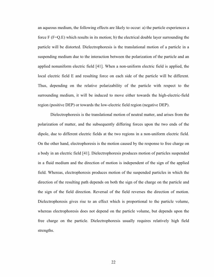
an aqueous medium, the following effects are likely to occur: a) the particle experiences a
force F (F=Q.E) which results in its motion; b) the electrical double layer surrounding the
particle will be distorted. Dielectrophoresis is the translational motion of a particle in a
suspending medium due to the interaction between the polarization of the particle and an
applied nonuniform electric field [41]. When a non-uniform electric field is applied, the
local electric field E and resulting force on each side of the particle will be different.
Thus, depending on the relative polarizability of the particle with respect to the
surrounding medium, it will be induced to move either towards the high-electric-field
region (positive DEP) or towards the low-electric field region (negative DEP).
Dielectrophoresis is the translational motion of neutral matter, and arises from the
polarization of matter, and the subsequently differing forces upon the two ends of the
dipole, due to different electric fields at the two regions in a non-uniform electric field.
On the other hand, electrophoresis is the motion caused by the response to free charge on
a body in an electric field [41]. Dielectrophoresis produces motion of particles suspended
in a fluid medium and the direction of motion is independent of the sign of the applied
field. Whereas, electrophoresis produces motion of the suspended particles in which the
direction of the resulting path depends on both the sign of the charge on the particle and
the sign of the field direction. Reversal of the field reverses the direction of motion.
Dielectrophoresis gives rise to an effect which is proportional to the particle volume,
whereas electrophoresis does not depend on the particle volume, but depends upon the
free charge on the particle. Dielectrophoresis usually requires relatively high field
strengths.
23
2.2.1 Comparison of Behavior of Neutral and Charged Bodies in Uniform and Non-Uniform Electric Fields
In uniform electric field, a charged particle is pulled along the field lines towards
the electrode carrying charge opposite to that on the particle. In the same field, a neutral
particle will be merely polarized [54]. Thus, a torque may be produced but no net
translational force may be seen, without which the body as a whole will not move
towards either electrode.
Figure 2.1 Comparison of the behavior of charged and neutral bodies when subjected to uniform and non-uniform electric fields.
In non-uniform electric field, the behavior of a charged body is the same as in a
uniform field i.e., it is attracted to the electrode of opposite polarity. The neutral particle
in this case is subjected to a net translational motion. This occurs because under the
influence of a non-uniform field the neutral body acquires a polarization that has an effect
of putting a negative charge on the side nearer the positive electrode, and a positive
charge on the side nearer the negative electrode. Since the particle is neutral, the two
charges on the body are equal, but the fields on the two regions are unequal thus giving
rise to a net force.
24
2.2.2 Dielectrophoresis
Dielectrophoresis is a term used to describe the polarization and associated
motion induced in particles by a non-uniform electric field. This phenomenon arises from
the difference in the magnitude of the force experienced by the electrical charges within a
dipole, induced when a non-uniform electric field is applied [41]. It is also described as
the translational motion of a particle in a suspending medium under the influence of a
nonuniform AC electric field. The application of a nonuniform AC electric field induces
a dipole moment in a charge-neutral particle, causing the particle to move toward a
region of maximum or minimum electric field strength. The driving direction depends on
the polarizability of the particle compared with that of the medium surrounding the
particle and the frequency of the applied electric field. If the polarizability of the particle
is more than that of the surrounding medium, it is called positive dielectrophoresis and
the particle tends to move towards the region of high field strength. On the other hand if
the particle is less polarizable than the surrounding medium the phenomenon is termed as
negative dielectrophoresis and the particle tends to move towards the region of low field
strength. Figure 2.2 shows the phenomenon of positive and negative dielectrophoresis on
particles under the influence of applied electric field. When an external electric field is
applied, the polarization and the associated motion induced in charge neutral particles,
describes the phenomenon of dielectrophoresis. This phenomenon occurs due to the
differences in the magnitude of the force experienced by the charges at each end of the
induced dipole. The magnitude of the force depends on the polarizability of the particle
relative to the surrounding medium [41].

25
Figure 2.2 Schematic diagram showing the positive and negative dielectrophoretic forces on particles subjected to non-uniform electric fields.
The dielectrophoretic force can be calculated by considering separately, the forces
acting on the negative and positive poles of the induced dipole which is oriented along
the x-axis. If the electric field vector is given by E= (Ex, 0, 0), the magnitude of force on
the negative pole located at coordinate x1 and having charge -q1 is:
)( 1xqEF x−=− (2)
Similarly the magnitude of force acting on the positive pole of charge +q at
position x2 is:
)( 2xqEF x+=+ (3)
Assuming the particle to be small and using the Taylor series to the first order, the
electric field variation over the particle’s length ‘h’ can be expressed as:
dx
dExhxExE xx += )()( 12 (4)
Therefore the strength of the dielectrophoretic force, FDE is given by the sum of F+ and F-
dx
dExqhFFFDE =+= −+ (5)

26
It can be seen from Equation-5 that FDE is proportional to the gradient of the
electric field. The dipole moment induced on the particle is a vector quantity whose
amplitude is given by:
xx Eqhpp αν===|| (6)
Where α - polarizability or the dipole moment per unit volume, ν - volume of the
particle and Ex-external field. From Equations 5 and 6 the dielectrophoretic force FDE is
given by:
dx
dExdx
dExEF xDE
2
21αναν == (7)
Equation-6 gives the x-component of the dielectrophoretic force. It can be seen
that this force is directly proportional to the square of the electric field intensity, thus
making it independent of the direction of electric field. Extending Equation-7 to a
generally directed electric field E= (Ex, Ey, Ez) which gives rise to an induced dipole
moment p= (px, py, pz) on the neutral particle, we have:
( ) EpEz
px
px
pF zyxDE ).(,, ∇=∂∂
∂∂
∂∂
= (8)
From Equation-6
||21).( 2EEEFDE ∇=∇= αναν (9)
From Equation-9 if ‘α’ (the dipole moment per unit volume) of the particle is positive,
then FDE increases as both the electric field and the gradient in field increase. As a result
the particles aggregate at regions with maximum electric field strength.
The magnitude and sign of ‘α’ depends on the permitivities and conductivities of
the particle and the suspending medium. The above analysis was made on the assumption

27
that the particles are more polarizable than the medium in which they are suspended,
which may not be the case always. If instead, the medium is more polarizable than the
particles suspended, then the dielectrophoretic force on the particles is strongest in the
regions where the electric field gradient is the least and the particles tend to move away
from the electrode edges where the electric field is usually high. This phenomenon is
called negative dielectrophoresis [54].
Given a polarizable sphere of permittivity ε p and volume ν in a medium of
permittivity ε m and subjected to an electric field of strength E, the induced moment p
will be given by:
( ) EErpmp
mp ανεεεε
π =+
−=
24 3 (10)
Substituting p in Equation-9, we get
( ) ||2
2 23 ErFmp
mpDE ∇
+
−=
εεεε
π (11)
To account for the observed variations of dielectrophoresis with frequency and
conduction, Equation-11 can be theoretically extended by including the conductivities,
and by replacing the simple dielectric constant ε with the complex absolute dielectric
constant or complex permittivity ωσ
εε iii
j−=* in the expression for FDE and by taking
the real part of its analogue. Thus the terms mε and pε will be replaced by the complex
quantities *mε and *
pε . Thus, we have:
||)],(Re[2 2**3 EfrF mpDE ∇= εεπ (12)
28
For a spherical homogenous particle f ( *pε , *
mε ) is referred to as the Clausius- mossotti
factor (C-M factor) [54]
=),( **mpf εε =
+
−**
**
2 mp
mp
εεεε
ωσσ
εε
ωσσ
εε
)2(2
)(
mpmp
mpmp
j
j
+−+
−−−
(13)
where, ω - Angular frequency, σm - Conductivity of the medium, σp -Conductivity of the
particle. From Equation-12 it is clear that the dielectrophoretic force depends not only on
the properties of the particles and the medium in which they are suspended but also on
the amplitude of the applied field. The force is attractive or repulsive based on the sign of
the real part of the C-M factor which in turn is a function of the frequency of applied
field.
Re [f ( *pε , *
mε )] = 0 at the cross over frequency, i.e. the particle is subjected to zero
dielectrophoretic force. At frequencies above the crossover frequency Re [f ( *pε , *
mε )] is
positive and for frequencies below the crossover frequency Re [f ( *pε , *
mε )] is negative.
The phenomena of positive DEP and negative DEP and its application in the present
design will be discussed in Chapter-3.
2.3 Experimental Setup
2.3.1 Setup for Measurement of Change in Resistance
Figure 2.3 shows the proposed experimental setup for detecting the change in
resistance when a particle flows through the electrode pairs in the measuring region.
Voltage divider method will be used to calculate the value of resistance under different

29
conditions: with no fluid in the channel (open circuit), with the fluid in the channel and
with particles suspended in the fluid. Without any fluid in the channel the value of
unknown resistance should be infinite as it is an open circuit and the voltmeter reads the
value of the applied DC voltage minus the voltage drop across the known resistance.
From the voltage divider rule the value of unknown resistance would be given by:
xs
xx VV
RVR−
= (1)
This method of resistance change calculation is suitable when there are just one or
two pairs of measuring electrodes. In the present case there are about eleven pairs of
measuring electrodes and thus the above mentioned method would prove to be complex.
Figure 2.3 Experimental setup for the measurement of change in resistance.
An impedance analyzer can be programmed with all pairs of electrodes connected
to it, thus measuring the impedance across each one of them. One advantage is that they
measure impedance (inductance, capacitance, and resistance) at spot frequencies or

30
across a range of frequencies. Thus impedance measurements can be performed at
multiple frequencies and the response of cells to different frequencies can be studied.
2.3.2 Setup for Dielectrophoretic Focusing
A function generator can be used to apply a wide range of voltages and
frequencies to the focusing electrodes so as to get to the maximum focusing efficiency of
the device. The choice of frequencies should be such that the particles are subjected to a
negative dielectrophoretic force which directs them to the center of the channel, thus
aligning them into a thin stream at the center. Thus, to achieve the optimum
dielectrophoretic focusing the device should be operated in conditions where the negative
dielectrophoretic force is the maximum. This can be possible by operating at frequencies
below the cross over value. Also, the value of applied voltages should be less than the
threshold for damaging the cells.
31
CHAPTER 3: DESIGN AND MODELLING
3.1 Overview of the Design
Two different designs for the micro-coulter counter are presented in this thesis.
Both designs are based on dielectrophoretic focusing of the cells, however, the difference
lies in the electrode geometry used for creating negative dielectrophoretic force to direct
the cells towards the center of the channel. The layout for both the designs are made
using LEDIT CAD tool. Several devices have been successfully fabricated using design1
which is a 4-mask process. The details of fabrication are explained in chapter4. The
layout and modeling of design2 are explained in detail in the present chapter.
The basic design of the device consists of mixing region, focusing region and a
measuring or sensing region. There are three main design issues to be considered for
efficient functioning of the device. The three regions of the device are shown in
Figure 3.1.
a) Fast and efficient mixing of the reagents
b) Efficient focusing of the cells to the center of the channel
c) Efficient sensing mechanism to record the passage of cells

32
Figure 3.1 Image showing the three regions in the device a) mixing region, b) focusing region, c) measuring or sensing region.
3.1.1 Mixing Region
Mixing of reagents is an important aspect in this study, as the experiments are
designed to monitor cellular volume after a change in the composition of the extra-
cellular solution. All cellular membranes are freely permeable to water and the net
movements of water between the cells and their surrounding interstitial fluid are
determined by the osmolalities of these two compartments [55]. If the osmolality of the
interstitial fluid decreases, fluid must enter the cells and the cell volume increases. On the
other hand if the osmolality of the interstitial fluid increases due to the increase in the
solute that does not penetrate through the cell membrane, water must leave the cells and
hence cell volume decreases. Thus the basic physiological mechanisms that determine
and control the osmolality of the extra-cellular fluid affect the cellular volume. Here, the
micro-fluidic system allows two different media to be merged in a Y-shaped channel. For
example, suppose the cells are at equilibrium with the surroundings and the concentration
A B C

33
is 290 mOsm. Call this solution A. Consider another solution B at a concentration of
1200 mOsm without cells. If we have A and B in separate inlets, input them at the same
rates, and assume good mixing, then we will essentially measure the volume reactions of
the cells after exposure to the average of the two osmolalities 745 mOsm. In this case we
would measure the cell shrinking or the cellular volume change as a function of time.
However, conventional mixing schemes cannot be used in micro devices due to
the absence of turbulence. Hence, molecular diffusion stands out as the only way to
achieve mixing in these devices [45]. But this process takes a considerable amount of
time and thus limits the performance of the system. This method is particularly
ineffective in biological processes that involve large molecules, since the diffusion
coefficient due to Brownian motion is inversely proportional to the size of the molecule.
The efficiency of mixing is directly related to the area of interface between two fluids
being mixed, greater the area of interface implies greater efficiency. The device discussed
in this thesis uses a serpentine shaped channel designed for passive mixing of the
reagents through chaotic advection. Passive mixing is chosen due to the inherent
advantages such as simple operation because the mixing occurs structurally, thus making
them suitable for integration with different kinds of miniaturized components. The
mixing in passive systems is by virtue of their geometry and any natural flow features
that arise [56]. Also, it is more reliable and requires no external power source which is
advantageous mainly in portable micro devices.
3.1.2 Focusing Region
As already discussed in Chapter-2, the phenomenon of dielectrophoresis is
classified into two types i.e., positive DEP and negative DEP. In the device presented
34
here, negative dielectrophoresis is used to focus the particles into the center of the
channel. Non-uniform AC electric fields are used to induce polarization which also
results in the subsequent motion of the particles. In the case of positive dielectrophoresis
the particles are directed to regions of high electric field strength, whereas in negative
dielectrophoresis they are directed to regions of low electric field strength. This
movement of particles depends on the applied frequency and also on the dielectric
properties of the particle and the medium suspending the particles.
The electrodes used for focusing in Design-1 are vertical side wall electrodes
electroplated on either side of the channel to a thickness of about 16µm which is
comparable to the height of the channel. With vertical side wall electrodes, there will be a
uniform distribution of electric field throughout the height of the channel. In this case, by
changing the configuration of electrodes, a non-uniform electric field can be generated
along the width of the channel, which is uniform along the height of the channel. By
changing the parameters of the applied field a negative dielectrophoretic force can result
directing the cells to the center of the channel away from the electrode edges where the
electric field is highest. On the other hand, the electrodes used for focusing in Design-2
are interdigitated electrodes fabricated along the circumference of the channel so that the
cells experience negative dielectrophoretic force from all the directions and tend to move
to the low electric field region present at the center of the channel.
3.1.3 Sensing or Measuring Region
Resistive pulse technique is used for counting and sizing of the particles. A series
of asymmetrically placed electrode pairs are used for recording the resistance changes
when a cell passes through them. The measuring region was made very long and
35
electrode pairs were patterned in such a way that they are very close to each other at the
beginning (~50µm) of the channel compared to the rest of the channel where they are
spread appropriately (~ 2-5mm). This was done in order to get more data at the beginning
of the time course experiment i.e., when the sample solution containing the cells mixes
with the buffer solution, than at the end. In this way the cellular volumetric change, due
to the change in extra cellular media contents can be measured as the cell passes through
the measuring channel.
3.2 Design-1
Design-1 is a four mask design fabricated on a glass substrate. The coulter counter
is designed with three regions i.e., mixing region, focusing region and measuring region
and is patterned in a thick SU8 layer. The electrodes used for dielectrophoretic focusing
and those used for measuring the resistance changes are made of electroplated gold,
electroplated on both side of the channel along its width thus forming vertical side wall
electrodes. This enables the application of electric fields in the lateral direction to
manipulate the fluid flow or particles in the channel.
Wang et al. [57] modeled different electrode configurations in three dimensions to
derive an electric field distribution in each case. The first electrode pattern is that of
planar electrodes which are directly deposited and patterned on the substrate. It was
observed that the electric field distribution was highest at the electrode surface and
decreases vertically away from the electrodes. The second electrode configuration was
that of metal layers patterned on the trapezoidal walls of the channel created by
anisotropic etching. It was observed that the electric field was concentrated near the
electrode edges at the bottom of the channel which was about four orders of magnitude

36
greater than that at the top of the channel. The third and last electrode configuration is
that of vertical electrodes on either side of the channel. It was seen that there was a
uniform distribution of electric field throughout the height of the channel. In this case, by
changing the configuration of electrodes, a non-uniform electric field can be generated
along the width of the channel, which is uniform along the height of the channel. The
layout of the masks for Design-1 is done using LEDIT CAD tool. The four masks used
for the design are shown in Figure 3.2.
The electrode mask (Figure 3.2a) is used for patterning the trenches for
electroplating the gold tabs. The trace and bonding pad mask (Figure 3.2b) is used for
patterning the electrode traces and bonding pads for the electroplated gold tabs. The
bonding pads will be used for wire bonding and for connection with the external
circuitry. The channel mask (Figure 3.2c) is used for patterning the micro-fluidic channel
using SU8 which is a negative photoresist. Lastly, the connector mask (Figure 3.2d) is
used for marking the appropriate positions of the fluid inlets and outlet. The details of
fabrication are explained in Chapter 4.
3.2a) Electrode mask used for patterning the trenches which will be used for electroplating.

37
3.2b) Trace and bonding pad mask used for patterning the electrode traces and bonding pads.
3.2c) Channel mask used for patterning the channel in SU8.
3.2d) Connector mask used for patterning the positions of the fluidic connectors.
Figure 3.2 Images showing the masks used in the fabrication.

38
3.3 Design-2
The Coulter counter is designed with interdigitated electrodes along the
circumference of the channel to create a negative dielectrophoretic effect to focus the
particles to the center of the channel. The array of electrodes is fabricated on the
circumference of the rectangle like channel. With this arrangement the electric field in the
channel is distributed in such a way that the minimum electric field region lies in the
center of the channel. Thus, the dielectrophoretic forces direct cells from all directions to
the center of the channel. It is a seven mask design on a silicon substrate. It is more
complicated compared to design-1 because of the number of masks involved and the need
for precise equipment to facilitate backside alignment.
Figure 3.3 Schematic diagram of design-2 showing the different components.
3.3.1 Description of Design-2
A schematic view of the Coulter counter mask layout is shown in Figure 3.4.
Top electrodes
Bottom electrodes
Fluid flow
Channel outlet
Fluid inlet port
Channel inlet
Focusing electrodes
Fluid outlet port

39
a) Oxide mask-1 (Photomask-1) b) Oxide mask-2 (Photomask-2)
c) Bottom electrode mask (Photomask-3) d) Sacrificial layer mask (Photomask-4)
e) SU8 and Parylene mask (Photomask-5) f) Top electrodes mask (Photomask-6)
g) SU8 channel mask (Photomask-7)
Figure 3.4 Pictures of all the masks for the fabrication of the device using design-2.

40
The first two photomasks (Oxide mask-1 (Figure 3.4a) and Oxide mask-2 (Figure
3.4b)) are used to create fluidic channels for inlet and outlet from the backside of the
wafer. Bottom set of interdigitated electrodes is patterned and defined using photomask-3
(Bottom electrode mask (Figure 3.4c)). A thick photoresist sacrificial layer, used to create
the channel is patterned using photomask-4(Sacrificial layer mask (Figure 3.4d)).
Trenches for the top set of electrodes are patterned in the parylene and SU8 layers using
photomask-5 (SU8 and Parylene mask (Figure 3.4e)). The upper set of interdigitated
electrodes are patterned using photomask-6 (Top electrodes mask (Figure 3.4f)). The
thick SU8 layer which forms the channel structure and supports the channel is patterned
using photomask-7 (SU8 channel mask (Figure 3.4g)).
Figure 3.5 Schematic of the layout for design-2.
Figure 3.6 A part of the rectangular electrode array forming the micro-fluidic channel.
Interdigitated electrodes configuration for focusing
Measuring electrodes

41
Figure 3.5 shows a schematic of the top view of the masks used for Design-2 with
the interdigitated electrodes configuration. Another proposed design was to increase the
number of measurements by having 2 to 3 measuring regions (like the one showed in
Figure 3.5) in series. This device will be fabricated in the later stage of the project. The
electrode configuration used for modeling Design-2 is shown in Figure 3.6.
3.3.2 Modeling of Design-2
The modeling of Design-2 in two-dimensions was done using Silvaco. The
electrodes were modeled as planar electrodes on either side of the channel, and the
electric field distribution in the channel was observed. Figure 3.7 shows the result
obtained when the length of the electrodes (anode and cathode) is 20µm and the gap
between adjacent electrodes (between an anode and adjacent cathode) is 5µm and the
voltage was fixed at 15V. The graph on the left gives the electric field distribution in the
center of the channel along its length.
Figure 3.7 Result obtained with: length of electrodes= 20µm; gap between adjacent electrodes= 5µm; V=15V.

42
Figure 3.8 Result obtained with: length of electrodes= 10µm; gap between adjacent electrodes= 10µm; V=15V.
Figure 3.8 shows the result obtained when the length of the electrodes is 10µm
and the gap between adjacent electrodes is 10µm and the voltage is fixed at 15V. From
the two results obtained it can be seen that the electric field at the center of the channel is
relatively less in the second configuration compared to the first. Table 3-1 gives a list of
the different electrode configurations (length of electrodes and gap between adjacent
electrodes) that were studied.
In all the cases the voltage is fixed at 15V, the width of the channel was fixed at
40µm and the thickness of the electrodes was fixed at 200nm. From the above results it
can be seen that the electric field is highest at the electrode surfaces and decreases as we
move away from the electrodes. If the distance between the electrodes is decreased to less
than 5µm or greater than 30µm, the electric field intensity is sufficiently high in the
center of the channel. This concept was used to model the interdigitated electrodes array

43
in three dimensions. The analysis of this design is done using CST Microwave studio.
The electrodes were modeled as a rectangular array and a voltage is applied between
alternate electrodes at different frequencies.
Table 3-1shows the various configurations of electrodes studied using Silvaco, V=15V, Width of the
channel=40 µm and Thickness of electrodes = 200nm.
Width of Electrodes (µm)
Distance between adjacent Electrodes (µm)
10 10 10 15 15 10 20 10 30 10 30 5 100 10 100 5 150 5
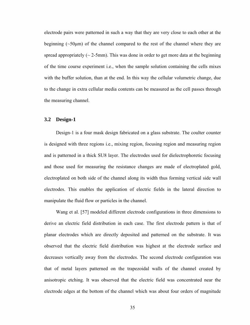
Figure 3.9 Electric field distribution with: width of electrodes=40µm; gap between adjacent electrodes=10µm; width of channel=100µm; height of the channel=50µm.
Minimum electric field region at the center of the channel
High electric field
44
Figure 3.9 gives the electric field distribution at the center of the channel in the x-
plane. The width of electrodes is 40µm, distance between adjacent electrodes is 10µm,
width of channel is 100µm and height of the channel is 50µm. It can be seen that region
of least electric field lies towards the center of the channel and the region of high electric
field is present at the electrode edges. A similar result can be seen when the dimensions
of the rectangular array were changed (Figure 3.10). Here, the width of the electrodes is
60µm, distance between adjacent electrodes is 10µm, height of the channel is 40µm and
width of the channel is also 40µm. The electric field minimum in this case can also be
seen at the center of the channel.
Figure 3.10 Electric field distribution with: width of electrodes=60µm; gap between adjacent electrodes=10µm; width of channel=40µm; height of the channel=40µm.
Several different designs are modeled by varying the width of the electrodes, the
distance between two adjacent electrodes, height and width of the channel. Table 3-2
gives the different configurations of the channel that have been studied. The first three
configurations indicate a minimum electric field in the center of the channel which is
Minimum electric field region at the center of the channel

45
desired. The layout of this design is made using LEDIT with different types of mixing
regions such as straight, single serpentine and double serpentine shaped channel.
Table 3-2 shows the different electrode configurations studied using CST Microwave Studio.
Width of the channel (µm)
Height of the channel (µm)
Width of Electrode (µm)
Distance between adjacent electrodes (µm)
Frequency (KHz)
Voltage (V)
100 50 40 10 10 10 40 40 60 10 10 10 100 30 150 40 10 10 100 30 115 20 10 10 100 30 115 20 10 15 100 30 115 10 10 15

46
CHAPTER 4: FABRICATION AND PACKAGING
4.1 Materials Used in the Fabrication
The techniques used in the fabrication of Microelectromechanical systems have
deviated from the standard techniques that were being used in the Integrated circuit
fabrication. A wide variety of materials such as polymeric materials, plastics etc. are
being used in the fabrication in addition to the silicon, glass and other microelectronic
materials [58]. The choice of materials used in the fabrication of micro devices for
biochemical and biological processes especially those involving cells, is very important
as not all materials are biocompatible and thus choice of the wrong material could cause
cell lysis [59]. The following is a brief description of all the materials used in the
fabrication of the micro-coulter counter.
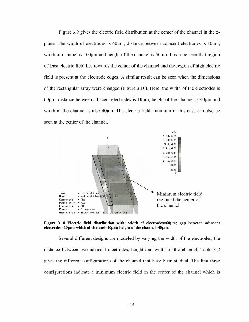
4.1.1 Metals
Medical micro-devices, biochemical devices and surgical implants have all been
developed utilizing a number of different materials including metals. Biocompatibility of
a device, to a large extent depends on the chemical and physical nature of the materials
used. Since the device deals with living cells, the choice of metals used is very important,

47
as some of the metals commonly used in microfabrication applications such as
chromium, nickel, iron, aluminum and copper are not biocompatible. However, Tungsten,
Platinum, Iridium, Titanium and Gold are some of the metals widely being used in the
fabrication of biomedical devices because of their biocompatibility and a good cellular
response in biological applications [60]. The metals used in the fabrication of this device
are Titanium (Ti) and Gold (Au).
4.1.1.1 Titanium
Titanium has good adhesion to silicon, silicon dioxide and glass and is frequently
used as an adhesion layer for less adhesive metals such as gold. Some of the unique
properties of Ti are its light weight, high durability in extreme environments, high
strength and biocompatibility [61]. In this work, Ti is used as an adhesion layer for Au. It
is sputter deposited using Magnetron sputtering system (Figure 4.1).
Figure 4.1 Sputtering system
48
4.1.1.2 Gold
Gold is chosen as the metal for the electrodes because of its biocompatibility,
ductility, high electrical conductivity, resistance to corrosion and lack of toxicity. Also,
the deposition and etching of Au is a well established process in microfabrication.
Magnetron sputtering system is used to deposit thin layers of Au, to a thickness of < 1µm.
However, for very thick Au depositions (tens of microns), a process called electroplating
can be used (Figure 4.2).
Figure 4.2 Image of the Electroplating setup.
4.1.2 SU8 as the Channel Material
The SU-8 is an EPON SU-8 epoxy resin (from Microchem) that has been originally
developed, and patented (US Patent No. 4882245 (1989) and others) by IBM. It is widely
Techni Gold 25 ES gold electroplating solution
Hotplate with magnetic stirrer
Power Supply
Multimeter
Clips for holding the anode and cathode

49
used in micromachining and other microelectronic applications [62]. Some of the
desirable features of SU8 are [63]:
- Suitable for fabrication of structures with a high aspect ratio (ratio of height and
width of the structure) and smooth side walls.
- Biocompatibility.
- Excellent mechanical properties.
- Suited for permanent applications, where it is cured and left as a part of the
system.
- High optical transparency above 360nm.
- Fabrication of SU8 does not require expensive masks and can be done using
standard photolithography techniques.
- Insulating property of SU8.
- High chemical resistance.
Unlike other common photo resists, SU8 is a negative photoresist epoxy which means
that the portions of SU8 exposed to UV light gets solidified due to the cross linking of the
molecular chains in its structure [64]. The exposed, cross linked resist is insoluble in
organic developers, while the unexposed uncross linked resist dissolves in SU-8
developer, thus forming a negative image of the mask. It can be spun to a thickness
ranging from a few micrometers to about one or two millimeters, and can still be
processed using a standard mask aligner. The process steps for SU8 channel fabrication
are given in Appendix-A.
50
4.1.3 Polydimethylsiloxane (PDMS)
There has been a constant search for new materials and methods for fabricating
micro-fluidic devices, as etching in Si and glass is expensive and also time consuming
[65]. Si is expensive and is also opaque in the visible/ UV region of the spectrum which
makes it unsuitable for applications that involve optical detection. The fabrication using
Si requires regular access to the clean room [66], also the chemical compatibility and
physical and optical properties can be problematic for some applications. Although glass
is transparent, the vertical side walls are difficult to etch as it is an amorphous material.
Researchers have been looking for alternative cheaper materials which could replace the
traditional materials. Many micro-devices have been fabricated using a variety of
polymer materials such as poly (methylmethacrylate) (PMMA), polyvinylchloride (PVC),
poly (dimethylsiloxane) (PDMS) etc [67]. These polymer materials prove to be a
promising alternative for the production of micro-fluidic devices as they are relatively
less expensive, great diversity in material property to suit a particular application, high
flexibility, biocompatibility and ease of fabrication when compared to the traditional
materials like silicon [68 69]. Soft lithography refers to a non-photolithographic
technique of fabricating micro structures using soft elastomeric materials such as PDMS
[70]. It provides a simple, low cost and effective method of fabricating micro- and nano-
structures. A master mold is first created by microfabrication techniques such as
photolithography, micromachining etc, PDMS (10:1 mixture of Sylgard 184 elastomeric
base and Sylgard 184 curing agent) is poured over the master and left to cure. PDMS can
be cured by leaving it for 24hrs at room temperature of by placing it in an oven for 1hour
minutes at 65°C. Once cured, PDMS can be peeled off from the master mold. Figure 4.3

51
shows an illustration of the procedure for fabricating PDMS stamps using soft
lithography.
Figure 4.3 Illustration of the procedure for fabricating PDMS stamps.
Some of the advantages of PDMS are: it is soft and makes conformal contact with
the surface, optically transparent, non-toxic, inexpensive, chemically inert and durable
[65].
4.2 Fabrication
4.2.1 Fabrication Steps of Design-1
The fabrication of design-1 is based on simple surface micromachining processes.
The device is fabricated on microscopic glass slides as shown in
Figure 4.4. First, the glass slides were cleaned in a piranha solution (H2SO4: H2O2,
3:1) for 3minutes and then washed thoroughly with DI water. Two layers of Titanium and
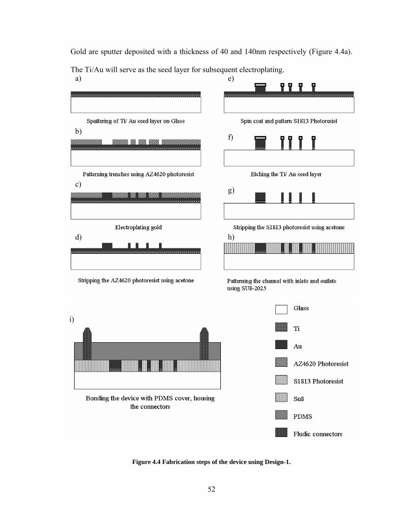
52
Gold are sputter deposited with a thickness of 40 and 140nm respectively (Figure 4.4a).
The Ti/Au will serve as the seed layer for subsequent electroplating.
Figure 4.4 Fabrication steps of the device using Design-1.
a)
b)
c)
d)
e)
f)
g)
h)
i)

53
Next a mold is created for electroplating the electrodes. The mold is created using
AZ4620 photoresist with a thickness of 16µm, spun on the wafer at 300 rpm for
15seconds and 1600 rpm for 20 seconds and baked on a hot plate at 110°C for 2minutes.
AZ4620 was patterned using the electrode mask (refer section-3.2) with patterns for
electroplating holes for the vertical electrodes. An electroplating setup was built and the
device was dipped into Technic gold 25 ES gold electroplating solution to plate the gold
electrodes at well controlled temperatures, stir rates and current densities (55°C and
300rpm). The thickness of the electroplated gold was measured and found to be about
12µm. After electroplating the AZ4620 mold was stripped using acetone and then rinsed
in DI water. A thin layer of S1813 photoresist was spun at 4000 rpm for 40seconds and
patterned using the trace and bonding pad mask (refer section-3.2) with patterns for the
electrode traces and bonding pads. The Ti/Au seed layer was etched, which results in a
device with electroplated electrodes and connecting leads. The next step is to define the
channel using SU8. A thick layer of SU8-2025 was spun at 500 rpm for 5seconds and
3000rpm for 20 seconds and soft baked at 65°C for 2minutes and 95°C for 5minutes.
Channel mask (refer section-3.2) was used to pattern the channel in SU8. The device was
postbaked at 65°C for 1minute and 95°C for 3minutes and later developed in PEGMA
developer for about 6 to 7minutes. It was then washed with IPA and hard baked at 120°C
for 15minutes. Connector mask (refer section-3.2) is used to mark the positions of the
fluidic connectors on a microscopic glass slide. Fluidic connectors (from Harward
Apparatus.Inc) are temporarily fixed on the marked positions using quick glue (from
Radioshack). Once the fluidic connectors are properly fixed these glass slides are placed
in a petri dish for the PDMS processing.

54
Figure 4.5 Picture of the complete fabricated device with the PDMS cover and fluidic connectors.
A 10:1 mixture of PDMS base and curing agent is prepared and poured in a Petri
dish and left overnight for it to cure. The cured PDMS slab along with the embedded
fluidic connectors is then peeled off from the Petri dish and cut into cubes of desired sizes
and is used to seal the channel.
Figure 4.6 Mask for Patterning the PCB package.
The device is then packaged on a copper coated PCB board patterned with the
bonding pads for external connections (Figure 4.6). The fluid flows through tubes fitted
Fluidic connectors PDMS
Cover
Device with Au electrodes and SU8 channel
400µm
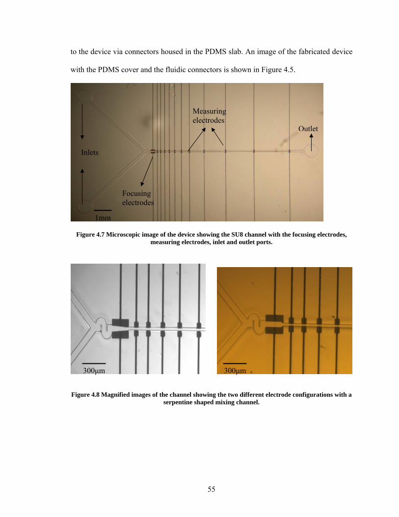
55
to the device via connectors housed in the PDMS slab. An image of the fabricated device
with the PDMS cover and the fluidic connectors is shown in Figure 4.5.
Figure 4.7 Microscopic image of the device showing the SU8 channel with the focusing electrodes, measuring electrodes, inlet and outlet ports.
Figure 4.8 Magnified images of the channel showing the two different electrode configurations with a
serpentine shaped mixing channel.
Outlet
Inlets
Focusing electrodes
Measuring electrodes
300µm 300µm
1mm
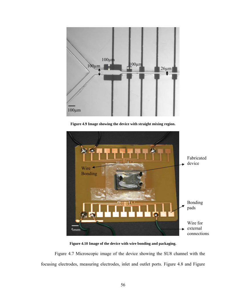
56
Figure 4.9 Image showing the device with straight mixing region.
Figure 4.10 Image of the device with wire bonding and packaging.
Figure 4.7 Microscopic image of the device showing the SU8 channel with the
focusing electrodes, measuring electrodes, inlet and outlet ports. Figure 4.8 and Figure
Bonding pads
Wire for external connections
Fabricated device
Wire Bonding
100µm 100µm
100µm 26µm
100µm
5mm

57
4.9 show the microscopic images of the fabricated channel with different channel
geometries and electrode configurations. Figure 4.10 shows the complete device with
wire bonding, packaging and soldering for external connections.
4.2.2 Fabrication Steps of Design-2
This section gives a detailed description of the proposed fabrication steps for
design-2. The first step in this design is to deposit a thin layer (~ 2µm) of SiO2 on both
sides of a silicon wafer for insulation. A layer of photoresist is spin coated on the back of
the wafer and Oxide mask-1 (photomask-1, Figure 4.11a) is used to pattern the
photoresist on the back followed by etching of the SiO2 layer to define portions of the
wafer that will be subsequently etched. Later, the photoresist is washed off using acetone
and through holes are etched in silicon wafer until the top layer of SiO2 is reached. Oxide
mask-2 (Photomask-2, Figure 4.11b) is used to protect parts of the SiO2 layer and the
remaining parts are etched to define the region between the fluid input port and the
channel inlet and the channel outlet to the fluid output port. Next, a layer of metal (Au) is
deposited on top of the wafer and Bottom electrode mask (photomask-3, Figure 4.11c) is
used to pattern it, followed by etching off the remaining metal thus forming the bottom
electrodes. A layer of thick photoresist (~40µm) is spin coated on the wafer which acts as
a sacrificial layer. A sacrificial layer mask (photomask-4, Figure 4.11d) is used to pattern
this layer in the shape of the channel. Next, a layer of parylene is deposited on the wafer
followed by spin coating a layer of SU8. SU8 and Parylene mask (photomask-5, Figure
4.11e) is used to pattern the SU8 layer and also to etch the parylene layer. Later, a layer
of metal (Au) is deposited on the wafer and patterned to form the top set of electrodes
using Top electrodes mask (photomask-6, Figure 4.11f). The remaining parts of the metal

58
are etched using a gold etch solution. The next step is used to spin coat a thick SU8 layer
and pattern it in the shape of the channel using SU8 channel mask (photomask-7, Figure
4.11g). Oxide mask-1 (photomask-1) is used to etch out portions of the SiO2 layer from
the back of the wafer, thus creating openings for the fluid flow through and out of the
channel. The photoresist sacrificial layer is then removed which forms the channel for the
fluid flow. The last step is to bond the device with glass on the backside for stability and
imaging using an inverted microscope.
4.11a) Image showing the oxide mask-1 (Photomask-1) and the cross-section view of the device
4.11b) Image showing the oxide mask-2 (Photomask-2) and the cross-section view of the device
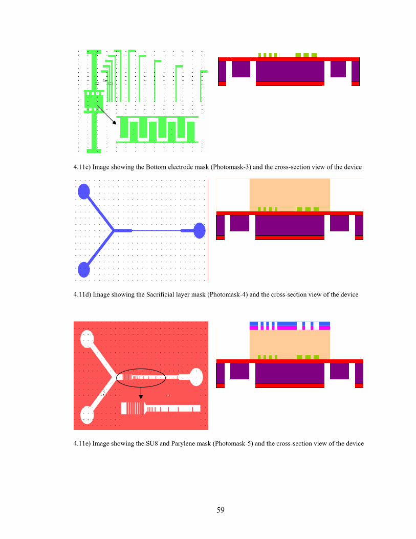
59
4.11c) Image showing the Bottom electrode mask (Photomask-3) and the cross-section view of the device
4.11d) Image showing the Sacrificial layer mask (Photomask-4) and the cross-section view of the device
4.11e) Image showing the SU8 and Parylene mask (Photomask-5) and the cross-section view of the device

60
4.11f) Image showing the Top electrodes mask (Photomask-6) and the cross-section view of the device
4.11g) Image showing the SU8 channel mask (Photomask-7) and the cross-section view of the device
4.11h) Image showing the cross-section of the complete device after etching out the holes for inlet and outlet, removal of sacrificial layer and glass bonding.
Figure 4.11 Pictures of all the masks for the fabrication of the device using Design-2

61
CHAPTER 5: RESULTS AND DISCUSSION
5.1 Approach to Device Testing
The following are the tests to be conducted to have a fully working device:
- The fluid flow through the channel has to be tested to make sure that there is no
leakage of fluid throughout the channel.
- Mixing efficiency of the device has to be tested to make sure that the two fluids
introduced into the channel are properly mixed before they enter the measuring
region of the channel. Two fluids of different colors (say blue and yellow) can be
introduced through the two inlets and the mixing region can be examined to
determine if the mixing is efficient.
- The sensing region has to be tested by measuring the change in impedance when a
particle passes through a pair of electrodes. Initially, latex beads of different sizes
can be used to test the device. An impedance analyzer can be used to test the
change in impedance when the particle passes through all the electrode pairs
sequentially.
- Finally, the focusing efficiency of the device has to be tested. By varying the
applied voltage and frequency of the AC supply, an optimum negative
dielectrophoretic force for focusing the particles can be determined.

62
5.2 Fluid Flow in the Channel
The fluid flow is tested by flowing ethanol through the channel by using a syringe
pump. Several experiments were conducted to improve the device performance using the
setup shown in Figure 5.1.
Figure 5.1Setup for fluidic testing
5.2.1 Glass Cover to Seal the Channel
Initially, a glass slide is used to seal the channel. Holes are drilled in the glass
slide for the inlet and outlet ports. A thin layer (5µm) of SU8 2005 is spin coated on glass
at 3000rpm for 20seconds and soft baked at 65°C for 1 minute and 95°C for 3 minutes.
This glass slide is then bonded to the device and baked at 100°C for 10minutes. Fluidic
connectors are placed on the holes drilled in the glass slide and thick SU8 2025 is poured
around it and left overnight at room temperature. A blue colored dye is added to ethanol
and made to flow through the device at different flow rates (1-10µl/min). A leakage of
Syringe pump
Device
Tubing

63
fluid in the channel is observed. Figure 5.2 shows the leak of fluid in the mid-section of
the measuring channel.
Figure 5.2 Microscopic image showing the leak in the mid-section of the channel
Since glass is brittle it does not conform to the non-uniformities present on the
surface of the SU8 channel, thus creating voids at the glass-device interface which results
in the leakage of fluid. Several alternative techniques of using glass to seal the channel
such as varying the thickness of SU8 spun on glass, varying the temperature and duration
of soft bake, have been tried. However, fluid leaks were observed in all the cases.
5.2.2 PDMS to Seal the Channel
An alternative method to avoid fluid leakage in the channel is to replace the glass
cover with some flexible material. Polydimethylsiloxane (PDMS) is chosen, due to its
advantages such as flexibility, biocompatibility, and ease of fabrication, cost efficiency
and transparency. Also, PDMS processing is simple and does not require clean room
Leak of fluid in the channel
30µm
10µm latex bead
30µm

64
facility. Since PDMS is a rubber like material and it is highly flexible, it conforms to the
curvature of the surface it comes into contact with. A mold is prepared by sticking the
connectors on a glass slide and by placing it in a Petri dish. A 10:1 mixture of PDMS
base and curing agent is prepared and poured in the Petri dish and left at room
temperature for 24hrs or in an oven at 90°C for 20 minutes. The cured PDMS is later cut
into cubes and peeled off from the mold. The PDMS sheet is then spin coated with a thin
layer of SU8 2005 (about 5µm). If SU8 is directly spin coated on the PDMS sheet, it
shrinks to the center of the sheet when baked as PDMS is very hydrophobic. One method
to make the surface of PDMS hydrophilic is to treat it with oxygen plasma. SU8 spreads
uniformly and adheres to the treated PDMS surface after baking. The PDMS sheet with
spun SU8 is baked on a hotplate at 90°C for 10minutes. The PDMS sheet is then aligned
to the channel on the device and the whole device is then baked at 65°C for 10minutes by
applying enough pressure by placing a weight on top of it. The device is then exposed to
UV light for 40seconds and later hard baked at 120°C for 20minutes to crosslink the SU8
layer and to glue the PDMS sheet to the channel.
The connectors are then placed in the holes on the PDMS cover and PDMS
mixture was poured around them and allowed to cure to make sure they are properly
fixed in position. This device is tested for fluid flow and as shown in Figure 5.3 there is
no leaking of fluid in the channel.
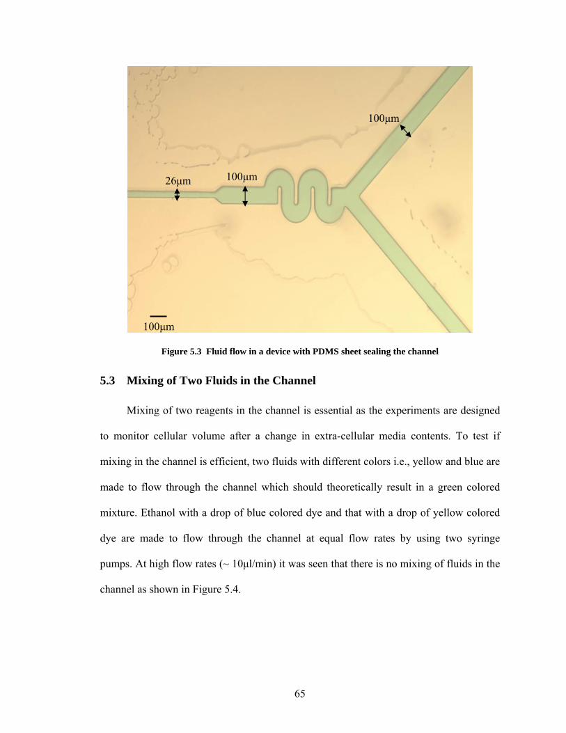
65
Figure 5.3 Fluid flow in a device with PDMS sheet sealing the channel
5.3 Mixing of Two Fluids in the Channel
Mixing of two reagents in the channel is essential as the experiments are designed
to monitor cellular volume after a change in extra-cellular media contents. To test if
mixing in the channel is efficient, two fluids with different colors i.e., yellow and blue are
made to flow through the channel which should theoretically result in a green colored
mixture. Ethanol with a drop of blue colored dye and that with a drop of yellow colored
dye are made to flow through the channel at equal flow rates by using two syringe
pumps. At high flow rates (~ 10µl/min) it was seen that there is no mixing of fluids in the
channel as shown in Figure 5.4.
100µm 26µm
100µm
100µm

66
Figure 5.4 No mixing seen at high flow rates
When the flow rate of one of the fluids was reduced to 2µl/min and the flow rate
of the other was 3µl/min, it was seen that although there is not a complete mixing of the
fluids in the mixing region of the channel, there is good amount of mixing in the
measuring region of the channel as shown in Figure 5.5.
Figure 5.5 Mixing at different flow rates.
Thus, the device was successfully fabricated with no fluid leak in the channel and
also a good mixing of reagents in the channel was achieved.
Good mixing seen further down the measuring channel
Incomplete mixing in the mixing region
Partial mixing at the start of the measuring region
No mixing seen in this region
26µm 26µm
100µm
26µm 100µm
100µm
100µm
26µm 26µm
67
CHAPTER 6: CONCLUSION AND FUTURE WORK
6.1 Micro Devices for Cell Sensing and Analysis
A large number of cell sensing devices have been developed due to their wide
spread applications in biochemical and medical fields. Also, a micro scale device adds to
the advantage owing to its small size and increased functionalities. This study involved
the fabrication of a micro scale coulter counter device which will be used for counting
and sizing different types of cells. The device presented here uses the phenomenon of
negative dielectrophoresis to focus the cells to the center of the channel and coulter
principle to detect cells based on the change in resistance when they pass through the
sensing zone. The design has been optimized to give a device with no fluid leakage which
is a major issue with most micro fluidic devices.
Another device was designed with interdigitated electrodes along the circumference
of the channel for dielectrophoretic focusing of the cells. This device also uses the coulter
principle to detect the passage of cells through the sensing zone. This device was
modeled using CST Microwave Studio and it was seen that for some configurations of
the electrodes, electric field was minimum at the center of the channel and thus by a
proper choice of applied voltage and frequency, optimum focusing of the cells can be
68
achieved. The applied voltage should not be too low as the dielectrophoretic force
becomes weak and cannot hold the particles in the center of the channel, also it should
not be too high that it causes cell damage.
6.2 Future Work
The device fabricated using Design-1 has to be electrically tested using the setup
discussed in Chapter-2. Latex beads of various diameters ranging from 1-15 µm will be
used to test and calibrate the system. Later different types of cells (refer section-6.2.1)
will be used to test the device. Also, various devices will be fabricated using design-2 and
similar tests will be conducted.
6.2.1 The Cell Types Primarily Being Considered
Mouse and rat spermatozoa cells which are available in relatively small numbers and
hence traditional Coulter counter methods prove to be disadvantageous. Additionally, the
cells adjust volumetrically very quickly to anisosmotic environments, equilibrating in less
than 10 seconds in many cases, making traditional Coulter Counter methods difficult or
impossible to implement.
Blood cells (particularly red blood cells) are the primary use for the traditional
Coulter counter as it counts the number of cells within a range of volume and gives
diagnostic information about blood contents. A micro Coulter counter will allow
significantly smaller volumes of blood to be used in such tests, and repeated
measurements of volumes (along the channel) will improve the accuracy and reliability.
Additionally, red blood cells, like sperm, adjust volumetrically very quickly to

69
anisosmotic environments, and traditional Coulter counter methods for measuring
volumes and fitting curves for red blood cell permeability do not work.
Oocytes volume measurement till date has been mostly limited to optical methods.
These methods are difficult to implement and most make some dubious assumptions on
the shape of the oocyte (e.g. cells shrink as spheres). A Coulter Counter method would
alleviate some of these problems. The challenge is that oocytes are only available in very
small (e.g. <100 cells) quantities. This makes traditional methods hard to implement.
Finally, working at different temperatures is a challenge for traditional coulter counter
methods, but with temperature controlled microscope stages, a micro coulter counter
technique would allow very precise control of experimental temperature.

70
REFERENCES
1. K. Nujufi, “Micromachined Micro Systems: Miniaturization Beyond
Microelectronics,” Proc. 2000 Symposium on VLSI Circuits Digest of Technical Papers, pp.6-13, 2000.
2. S. S. Saliterman, “Fundamentals of BioMEMS and Medical Microdevices,” SPIE
Press Monograph, vol. PM153, 2006.
3. M. Madou, ‘Fundamentals of Microfabrication: The Science of Miniaturization.’ Second Edition, CRC Press, 2002.
4. P. Zhang, G. A. Jullien, “Micromachined Needles for Microbiological Sample
and Drug Delivery System,” Proceedings of ICMENS2003, Jul 20-23, 2003.
5. R. Bashir, “BioMEMS: State-of-the-Art in Detection, Opportunities and Prospects,” Advanced Drug Delivery Reviews, vol. 56, pp 1565-1586, 2004.
6. Encyclopaedia Britannica Online: http://www.britannica.com/eb/topic-
101396/cell.
7. http://en.wikipedia.org/wiki/Organism#The_cell.
8. G. Fuhr and S. G. Shirley, “Cell Handling and Characterization Using Micron and Submicron Electrode Arrays: State of the Art and Perspectives of Semiconductor Micro Tools,” J. Micromech. Microeng, vol. 5, pp 77-85, 1995.
9. H. Andersson, A. Berg, “Microfluidic Devices for Cellomics: A Review,” Sensors
and Actuators B, vol. 92, pp 315-325, 2003. 10. M. J. Kellekoop, S. Kostner, “Chip Cell Handling and Analysis,” Institute of
Sensor and Actuator Systems, Austria. 11. L. M. Barrett, A. J. Skulan, A. K. Singh, E. B. Cummings and G. J. Fiechtner,
“Dielectrophoretic Manipulation of Particles and Cells Using Insulating Ridges in Faceted Prism Microchannels,” Anal. Chem, vol. 77, pp 6798-6804, 2005.
12. M. Yang, C. W.Li, and J. Yang, “Cell Docking and On-Chip Monitoring of
Cellular Reactions With a Controlled Concentration Gradient on a Microfluidic Device,” Anal. Chem., vol. 74, pp 3991-4001, 2002.

71
13. M. Castellarnau, N. Zine, J. Bausells, C. Madrid, A. Juarez, J. Samitier, A.
Errachid, ‘Integrated Cell Positioning and Cell-Based ISFET Biosensors’, Sensors and Actuators B, vol. 120, pp 615–620, 2007.
14. K. Avinash, Bhaskar and S. Menaka, “The State of MEMS in Automation,”
http://www.isa.org/Template.cfm?Section=Communities&template=/ContentManagement/ContentDisplay.cfm&ContentID=63192. Aug 2007,
15. L. Bertucco, G. Nunnari, C. Randieri, “A Cellular Neural Network Based System
for Cell Counting in Culture of Biological Cells,” Proc. IEEE, vol. 1, pp 341-345, 1998.
16. N. C. Hughes, S. N. Wickramasinghe, “Lecture Notes on Haematology,”
Blackwell Publishing, Seventh Edition, 2004. 17. http://en.wikipedia.org/wiki/Hemocytometer. 18. W. Groner, E. Simson, “Practical Guide To Modern Hematology Analyzers,” J.
Wiley & Sons company, 1995.
19. J. Z. Knapp, T. A. Barber, A. Lieberman, “Liquid and Surface-Borne Particle Measurement Handbook”, Informa Healthcare, First Edition, 1996.
20. http://www.beckmancoulter.com/coultercounterhomepage_tech_coulterprinciple 21. J. K. Nicholson, D. Stein, T. Mui, R. Mack, M. Hubbard, T. Denny, “Evaluation
of A Method for Counting Absolute Number of Cells With a Flow Cytometer,” American Society for Microbiology, vol. 4, no. 3, pp 309-313, May 1997.
22. J.H. Nieuwenhuis, F. Kohl J. Bastemeijer, P.M. Sarro, M.J. Vellekoop,
“Integrated Coulter Counter Based on 2-Dimensional Liquid Aperture Control,” Sensors and Actuators B, vol.102, pp 44–50, 2004.
23. R. S. Muller, “MEMS: Quo Vadis in Century XXI,” Microelectronic
Engineering, vol. 53, no.1, pp 47-54, June 2000.
24. J. C. Donald, D. C. Duffy, J. R. Anderson, D. T. Chiu, H. Wu, J. A. Schueller, G. M. Whitesides, “Fabrication of Microfluidic Systems in Poly(dimethylsiloxane),” Electrophoresis, vol. 21, pp 27-40, 2000.
25. W. K. Wu, C. K. Liang, J. Z. Huang, “MEMS-Based Flow Cytometry:
Microfluidics-Based Cell Identification System by Fluorescent Imaging,” Proc. of the 26th Annual International Conference of the IEEE EMBS, vol. 1, pp 2579-2581, 2004.
72
26. L. J. Kricka, “Miniaturization of Analytical Systems,” Clinical Chemistry, vol.
44, no.9, pp 2008–2014, 1998. 27. D. J. Beebe, G. A. Mensing, and G. M. Walker, “Physics and Applications of
Microfluidics in Biology,” Annu. Rev. Biomed. Eng, vol. 4, pp 261–286, 2002. 28. W. S. Maddux, J. W. Kanwisher, “An In Situ Particle Counter,” Limnology and
Oceanography, vol. 10, pp. 162-168, Nov 1965. 29. J. Zhe, A. Jagtiani, P. Dutta, J. Hu and J. Carletta, “A Micromachined High
Throughput Coulter Counter for Bioparticle Detection and Counting,” J. Micromech. Microeng. vol. 17, pp 304–313, 2007.
30. K. Roberts, M. Parameswaran, M. Moore and R. S. Muller, “A Silicon
Microfabricated Aperture for Counting Cells Using The Aperture Impedance Technique,” Proceedings of the 1999 IEEE Canadian Conference on Electrical and Computer Engineering, vol. 3, pp 1668-1673, 1999.
31. U. D. Larsen, G. Blankenstein, J. Branebjerg, “Microchip Coulter Particle
Counter,” Proceedings of the International Conference on Solid-State Sensors an Actuators, pp 1319-1322, 1997.
32. M. Koch, A. G. R Evans and A. Brunnschweiler, “Design and Fabrication of A
Micromachined Coulter Counter,” J. Micromech. Microeng, vol. 9, pp 159–161, 1999.
33. S. Gawad, L. Schild and P. Renaud, “Micromachined Impedance Spectroscopy
Flow Cytometer For Cell Analysis and Particle Sizing,” Lab on a Chip, vol. 1, pp76–82, 2001.
34. J. H. Nieuwenhuis, F. Kohl, J. Bastemeijerb, M. J. Vellekoopa, “First Particle
Measurements With an Integrated Coulter Counter Based on 2-Dimensional Aperture Control,” MTAS 2003 Seventh international conference on micro total analysis systems, pp 1219-1222.
35. M. G. Ormerod, “Flow cytometry: A Practical Approach,” Oxford University
Press, Third Edition, 2000. 36. Introduction to the Flow Cytometry Facility, University of Massachusetts,
Amherst. http://www.bio.umass.edu/mcbfacs/intro.htm
37. Introduction to Flow cytometry: A learning guide, Manual Part Number: 11-11032-01, April 2000.

73
38. G. B. Lee, C. I. Hung, B. J. Ke, G. R. Huang, B. H. Hwei, H. F. Lai,
“Hydrodynamic Focusing For A Micromachined Flow Cytometer,” Journal of Fluids Engineering, pp 672-679, vol. 123, Sep 2001.
39. R. R. Trujillo C. A. Mills, J. Samitier, G. Gomila, “Low Cost Micro-Coulter
Counter With Hydrodynamic Focusing,” Microfluidics and Nanofluidics, vol. 3, pp 171-176, 2007.
40. Y. Zhao, B. S. Fujimoto, G. D. Jeffries, P. G. Schiro, and D. T. Chiu, “Optical
Gradient Flow Focusing,” Optical Society of America, vol. 15, pp 6167-6176, 2007.
41. C. Yu, J. Vykoukal, D. M. Vykoukal, J. A. Schwartz, L. Shi, and R. C. Gascoyne,
“A Three-Dimensional Dielectrophoretic Particle Focusing Channel for Microcytometry Applications,” IEEE J.MEMS, vol. 14, no. 3, pp 480-487, June 2005.
42. Altendorf, D. Zebert, M. Holl, P. Yage, “Differential Blood Cell Counts Obtained
Using a Microchannel Based Flow Cytometer,” lnternational Conference on Solid-state Sensors and Actuators Chicago, Transducers, vol. 1, pp 531-534, June 1997.
43. http://en.wikipedia.org/wiki/Temporal_resolution 44. M. Wales, J. N. Wilson, “Theory of Coincidence In Coulter Particle Counters,”
Review of scientific instruments, vol. 32, no. 10, pp 1132-1136, Oct 1961. 45. H. Suzuki, N. Kasagi, C. M. Ho, “Chaotic Mixing of Magnetic Beads In Micro
Cell Seperator,” Proc. 3rd Int. Symp. Turbulence and Shear Flow Phenomena Sendai, Japan, pp 817-822, June 2003.
46. R. H. Liu, M. A. Stremler, K. V. Sharp, M. G. Olsen, J. G. Santiago, R. J. Adrian,
H. Aref, and D. J. Beebe, “Passive Mixing In a Three-Dimensional Serpentine Microchannel,” J.MEMS, vol. 9, no. 2, pp 190-197, June 2000.
47. Y. K. Lee, J. Deval, P. Tabeling and C. M. Ho, “Chaotic Mixing in
Electrokinetically And Pressure Driven Micro Flows,” The 14th IEEE Workshop on MEMS Interlaken, Switzerland, pp 483-486, Jan 2001.
48. J.Green, A.E.Hold, A.Khan, “A Review of Passive and Active Mixing Systems in
Microfluidic Devices,” Int. Jnl. of Multiphysics vol. 1, no.1, 2007. 49. N. T. Nguyen and Z. Wu, “Micromixers - A Review,” J. Micromech. Microengg,
vol. 15 R1–R16, 2005.
74
50. N. Y. Lee, M. Yamada, M. Seki, “Development of A Passive Micromixer Based
on Repeated Fluid Twisting and Flattening, and Its Application To DNA Purification,” Anal Bioanal Chem , vol. 383, pp 776–782, 2005.
51. P. K. Wong, T. H. Wang, J. H. Deval, and C. M. Ho, “Electrokinetics in Micro
Devices for Biotechnology Applications,” IEEE/ASME Transactions on Mechatronics, vol. 9, No. 2, pp 366-176, June 2004.
52. P. R. Gascoyne, J. Vykoukal, “Particle Separation by Dielectrophoresis,”
Electrophoresis vol. 23, pp 1973–1983, 2002. 53. IBMM: Microengineering and lab on a chip, School of Electronic Engineering,
University of Wales, Bangor. http://www.ibmm-microtech.co.uk/microeng/dielectrophoresis/science.php
54. H.A.Pohl, “Dielectrophoresis: The Behavior of Neutral Matter in Non-uniform
Electric Fields,” Cambridge University Press,1978. 55. D. C. Anthony, Macknight, A. Leaf, “Regulation of Cellular Volume,” J. Physiol,
vol. 57, pp 137-154, July 1977. 56. J. Green, A. E. Holdo, A. Khan, “A Review of Passive and Active Mixing
Systems in Microfluidic Devices,” Int. Jnl. of Multiphysics vol. 1, No.1, 2007. 57. L. Wang, L. Flanagan and A. P. Lee, “Side-Wall Vertical Electrodes for Lateral
Field Microfluidic Applications,” J.MEMS, vol. 16, No. 2, pp 454-461, April 2007.
58. R.Bashir, “BioMEMS: State-of-the-art In Detection, Opportunities and
Prospects,” Advanced Drug Delivery Reviews, vol. 56, pp 1565-1586, Elsevier, 2004.
59. D. Rickert, A. Lendlein, I. Peters, M. A. Moses, R. P. Franke, “Biocompatibility
Testing of Novel Multifunctional Polymeric Biomaterials for Tissue Engineering Applications in Head and Neck Surgery: An Overview”, Eur Arch Otorhinolaryngol, vol. 263, pp 215–222, 2006.
60. R. Acharya and W. Besio, “Comparing Auditory Middle Latency Response Using
Disc, Bipolar and Tripolar Concentric Ring Electrodes, http://www.ninds.nih.gov/funding/research/npp/niw06_abstracts.pdf
61. www.matweb.com

75
62. J. C. Ribeiro, G. Minas, P. Turmezei, R. F. Wolffenbuttel, J. H. Correia, “A SU-8
Fluidic Microsystem For Biological Fluids Analysis,” Sensors and Actuators A vol. 123–124, pp 77–81, 2005.
63. Microchem: NanoTM SU8 Negative Tone Photoresists, Formulations 50-100. 64. S. Tuomikoski, S. Franssila, “Wafer-Level Bonding of MEMS Structures With
SU8 Epoxy Photoresist”, Physica Scripta. vol. T114, pp 223–226, 2004. 65. J. C. Donald, D. C. Duffy, J. R. Anderson, D. T. Chiu, H. W. Olivier J. A.
Schueller, G. M. Whitesides, “Fabrication of Microfluidic Systems In Poly(dimethylsiloxane),” Electrophoresis , vol. 21, pp 27-40, 2000.
66. H. Makamba, J. H. Kim, K. Lim, N. Park, J. H. Hahn, “Surface Modification of
Poly(dimethylsiloxane) Microchannels,” Electrophoresis, vol. 24, pp 3607–3619, 2003.
67. H. Becker, L. E. Locascio, “Polymer Microfluidic Devices”, Talanta vol. 56, pp
267-287, Elsevier, 2002. 68. Y. H. Chen, W. C. Wang, K. C. Young, T. T. Chang, and S. H. Chen, “Plastic
Microchip Electrophoresis for Analysis of PCR Products of Hepatitis C Virus,” Clinical Chemistry vol. 45, no.11 pp 1938–1943, 1999.
69. S. A. Soper, S. M. Ford, L. Liu, M. Galloway, M. C. Murphy, D. Nikitopoulos
and K. Kelly, “Fabrication of Polymer-Based Microfluidic Devices using LIGA,”. 70. Y. Xia and G. M. Whitesides, “Soft Lithography,” Angewandte Chemie
International Edition, vol. 37, pp 550-575, 1998.

76
APPENDIX-A
This section describes the fabrication steps of the device in detail.
• Clean the Glass wafers: - Piranha, 3:1 mixture of Sulphuric acid and Hydrogen peroxide (add
peroxide to acid, not the other way). • Sputtering of Ti/Au seed layer: Thickness~180nm
- Ti-DC Deposition: Power=300W, Coat time= 400sec - Au-RF Deposition: Power=90W, Coat time= 1500sec
• Patterning trenches for electrodes: Use AZ4620 Photoresist - Spinner: 300-100-15/1600-300-20 (Speed- Ramp-Time) - Hot plate: 110°C for 2min - Exposure time: 22sec - Developer: AZ400k : DI = 1:3 - Developing time: 2min 25 sec
• Electroplating: - Voltage = 5V - Spin speed = 100rpm - Temperature of hot plate = 80°C - Current = 60mA - Time = 30min to 1hr (Depending on thickness)
• Wash off the AZ4620 Photoresist with Acetone • Patterning traces and bonding pads for the electrodes: Use S1813 Photoresist
- Spinner: 4000-1000-40 (Speed-Ramp-Time) - Hot plate: 90°C for 2min - Exposure time: 16sec - Developer: MF319 - Developing time: 1min 20sec
• Etching Au and Ti: - Au etching: KI:I2:DI water solution (1:4:10) for 2min - Ti Etching: HF:DI solution(1:100) for ~20sec

77
• Patterning the channel in SU8: Use SU8-2025
- Spinner: 500-100-5/3000-300-20 (Speed-Ramp-Time) - Soft Bake: 65°C for 2min ; 95°C for 5min - Exposure time: 17sec - Post exposure bake: 65°C for 1min ; 95°C for 3min - Developer: SU8 developer - Developing time:
a) First place the substrate in the developer for 4min b) Remove it from the developer and wash it with IPA c) Place it again in the developer for 2-3min d) Wash it with IPA ( do not use DI water to wash the substrate)
• PDMS cover for the channel: - Prepare PDMS slabs with holes for connectors: Use Sylgard 184
Elastomer: Curing agent = 10:1, Leave it for 24hrs at room temperature or place for 30min in an oven for it to cure.
- Immediately after the Oxygen plasma spin SU8-2005 on the PDMS slab: 300-100-5/3000-300-20 (Speed-Ramp-Time)
- Bake at 90°C for 10min - Align the PDMS cover with the device and bake at 65°C for 10min by
placing a weight on it. - Expose the device with the PDMS cover to U.V light for 40sec - Bake it again at 120°C for 20min - Place the connectors in the holes and seal them by pouring PDMS around
them. • Packaging on PCB:
- Purchase a PCB with Copper coating and cut it according to the dimensions of the device
- Spin coat S1813 photoresist on PCB: a) Spinner: 4000-1000-40 (Speed-Ramp-Time) b) Hot plate: 90°C for 2min c) Exposure time: 16sec d) Developer: MF319 e) Developing time: 1min 20sec
- Stick the device on PCB with a double sided tape - Bond the bonding pads on the device with the respective bonding pads on
the package by using a wire bonder or manually with Indium and Aluminum wire.