a high-efficiency high-power-density on-board low-voltage
TRANSCRIPT

0885-8993 (c) 2021 IEEE. Personal use is permitted, but republication/redistribution requires IEEE permission. See http://www.ieee.org/publications_standards/publications/rights/index.html for more information.
This article has been accepted for publication in a future issue of this journal, but has not been fully edited. Content may change prior to final publication. Citation information: DOI 10.1109/TPEL.2021.3076773, IEEETransactions on Power Electronics
IEEE POWER ELECTRONICS REGULAR PAPER/LETTER/CORRESPONDENCE
A High-Efficiency High-Power-Density On-Board Low-Voltage DC-DC Converter
for Electric Vehicles (EVs) Application Xiang Zhou, Member, IEEE, Bo Sheng, Student Member, IEEE, Wenbo Liu, Student Member, IEEE,
Yang Chen, Member, IEEE, Laili Wang, Senior Member, IEEE, Yan-Fei Liu, Fellow, IEEE and Paresh C. Sen, Life Fellow, IEEE
Abstract: On-board low-voltage dc-dc converter (LDC) in electric vehicles is used to connect the high voltage battery with the low voltage auxiliary system. With the advancement of auxiliary equipment in electric vehicles (EVs), the output current of the LDC can be hundreds of amperes, which will cause high conduction loss and severe thermal concern. In this paper, a high-efficiency high-power-density on-board LDC is presented. To reduce current stress and improve efficiency, three phase interleaved LLC dc-dc converters are paralleled to provide 270A load current. Synchronous rectifier (SR) is used to reduce secondary conduction loss. ZVS turn-on of primary switches and ZCS turn-off of secondary switches are achieved, thus switching loss can be reduced significantly. Moreover, phase-shedding technology is used to improve light load efficiency. Switch-controlled capacitor (SCC) technology is used to achieve accurate load current sharing among the three phases, which protects the devices against high current stress, reduces the conduction loss and improves the reliability of the system. As SCC switches achieve ZVS turn-on and turn-off by its nature, the loss of the SCC circuit is of less concern with regard to the rated output power. In addition, GaN HEMTs are used in the primary side to improve the power-density and eventually help achieving light weight. A 3.8kW (14V/270A) LDC prototype is developed and tested. Experimental results show good current balancing among the three phases. A peak efficiency of 96.7% at 140A load, and a full load efficiency of 95.8% are achieved with 3kW/L power-density and 1.5kg weight.
Keywords—Electric vehicles (EVs), LLC dc-dc converter, Synchronous rectifier, Switch-controlled capacitor
I. INTRODUCTION
With increasing environmental pollution caused by green-house gas emissions from conventional fossil fuel-driven vehicles, electric vehicles (EVs) are attracting increased attention as they are not only more environmentally friendly, but cheaper than fossil fuels vehicles [1]. Along with the development of electric vehicles (EVs), more and more auxiliary equipment, e.g. air conditioning, is required to satisfy consumer requirements. High power on-board low-voltage dc-dc converter (LDC) is essential in electric vehicles (EVs), which takes responsibility to transfer power from high-voltage battery to auxiliary equipment and low-voltage battery. As shown in Fig.
1, the battery system of EVs consists of high voltage (HV) Li-ion batteries (250V to 430V) and low voltage (LV) Lead-acid batteries (9V~16V). In general, HV batteries are used for traction of motor drives. LV batteries provide power for auxiliary equipment. As more and more auxiliary equipment is implemented in EVs to provide various additional features nowadays, such as lighting, audio/video systems, air conditioners, automatic seats, sunroofs, heated seats, etc., high load current level of LDC is the trend. From [1]-[2], at least 2.4kW power rating is required to supply auxiliary equipment. Therefore, the LDC should output more than 200A load at 12V.
Typically, EVs charger system operates at two modes, 1) the HV battery is charged from the grid by the off-board charger or the on-board charger when the vehicle is connected to the grid. 2) the HV battery provides power to auxiliary electronic devices or charges the LV battery through LDC when the vehicle is running [1]. In general, the voltage range of HV battery and LV battery system is wide. Galvanically isolated dc-dc converters are required in LDC to ensure safety and obtain high step-down voltage ratio (430V to 9V). Moreover, high power density and light weight are desirable for LDC due to the limitation on space and weight for EVs. Last but not least, high efficiency is required to extend the mileage per charge and to reduce the heatsink size.
Fig. 1. Diagram of EV power train
In [1], phase-shift full bridge converter is adopted in LDC. However, it is difficult to achieve ZVS for the lagging arm under light load. To guarantee ZVS of primary switches in LDC based on phase-shift full bridge converter, auxiliary inductors are used in [2]-[4]. In [5], a built-in buck circuit is used in transformer secondary of LDC to solve the induced voltage caused by the multi-winding high-frequency transformer.
In [1]-[7], phase-shift full bridge converter is adopted for LDC, and current-doubler circuit is utilized in the transformer secondary to provide high load current [1]-[3], [6]. However, compared to a phase-shift full bridge dc-dc converter, resonant
HV Li-ion Battery
Auxiliary LV Battery
On-Board Charger
DC-DC converter
Motor Traction converter
Speaker
Lamp
ect.
DC-DC converter
Manuscript received Feb 24, 2021; revised Apr 14, 2021; accepted Apr 27, 2021. (Corresponding Author: Laili Wang) X. Zhou and L. Wang are with the State Key Laboratory of Electrical Insulation and Power Equipment, Xi’an Jiaotong University, Xi’an 710049, China (e-mail: [email protected]; [email protected]). B. Sheng, W. Liu, Y. Chen, Y.-F. Liu and P C. Sen are with the Department of Electrical and Computer Engineering, Queen’s University, Kingston, ON K7L 3N6, Canada (e-mail: [email protected]; [email protected]; [email protected]; [email protected]; [email protected]).
Authorized licensed use limited to: Queen's University. Downloaded on May 02,2021 at 00:35:41 UTC from IEEE Xplore. Restrictions apply.

0885-8993 (c) 2021 IEEE. Personal use is permitted, but republication/redistribution requires IEEE permission. See http://www.ieee.org/publications_standards/publications/rights/index.html for more information.
This article has been accepted for publication in a future issue of this journal, but has not been fully edited. Content may change prior to final publication. Citation information: DOI 10.1109/TPEL.2021.3076773, IEEETransactions on Power Electronics
IEEE POWER ELECTRONICS REGULAR PAPER/LETTER/CORRESPONDENCE
converter such as LLC dc-dc converter benefits from that ZVS of primary switches and ZCS of secondary switches can be achieved, which is used widely in various application to achieve high-efficiency and high power-density [8]-[13].
In [14]-[17], LLC dc-dc converter is adopted in LDC of EVs. As output current is high in LDC, transformer secondary conduction loss is predominant. Thus, the efficiency could be improved significantly by using synchronous rectifier (SR) LLC dc-dc converter in [14]-[15]. To reduce transformer secondary current stress, two phase interleaved LLC dc-dc converter is used, and phase shedding technology is adopted to improve light load efficiency in [16]. [17] utilizes both LLC and B/DCM control schemes to improves efficiency and power-density.
Multi-phase dc-dc converters connected in parallel can help reduce the current stress, which makes an effective way to improve the efficiency. However, for the LDC based on LLC resonant converter, when switching frequency is close to series resonant frequency, the impedance of Lr and Cr in series is close to zero. Small tolerance on Lr or Cr will cause large impedance difference among different phases, thus the load current would be unbalanced severely and induce uneven heating of the circuit components. If current sharing cannot be achieved in multi-phase resonant dc-dc converters connected in parallel, one of the phases may carry all the output current and the other phases may carry no output current. This will degrade the efficiency, increase the current stress and even damage the board. Therefore, current sharing problem needs to be solved to improve the efficiency and reliability.
In [16], two separate voltage loop controllers are utilized in two-phase LLC dc-dc converters connected in parallel, which makes two phase current sharing by operating two phases at the different switching frequency. However, the different switching frequencies will cause beat frequency, which deteriorates the performance of the converter. In [18], two extra auxiliary PWM dc-dc converters are used to make two-phase LLC-DCX input current sharing. By transforming the current sharing of the resonant converter into PWM control of a dc-dc converter, this method is simple to implement. However, to make sure that the PWM converter only processes small partial power, the components tolerance of two DCX should be very small.
Current sharing can also be achieved by using series connection in multi-phase LLC converter with small resonant components tolerance [19]-[23]. Moreover, three-phase LLC dc-dc converter with Y connection or connection is also confirmed to achieve current sharing by series connection [21]-[23]. However, a serious current imbalance still occurs if large resonant component tolerance presents in three-phase LLC dc-dc converter. In addition, all three phases need to operate at the same time even with light load, thus, the light load efficiency will be degraded.
Compared to multi-phase LLC dc-dc converters connected in parallel directly, RMS input voltage of the resonant tank is lower in three-phase LLC dc-dc converter with Y connection or connection. The current stress of primary components in three-phase LLC dc-dc converter with Y connection or connection is higher under the same specification and the number of switches, which increases conduction loss. Therefore, multi-phase LLC dc-dc converters connected in parallel have the following advantages: 1) low current stress can reduce the
conduction loss; 2) unneeded phases can be shut down to improve the efficiency in light load condition.
To implement current sharing in multi-phase LLC dc-dc converters connected in parallel with the same switching frequency, several methods have been proposed in [24]-[30]. By adding capacitor, inductor, etc. passive impedance network so that the impedance of the resonant tanks are matched, good performance of current sharing is achieved in [24]-[27]. In [28]-[30], magnetic-coupling is adopted to achieve three phases current sharing. However, to achieve good current sharing performance, all these methods [21]-[30] required small resonant components tolerance. Otherwise, these methods will become ineffective.
Switch-controlled-capacitor (SCC) method is proposed in [31] to modify the resonant capacitor value so that resonant components tolerance can be compensated and current sharing among phases can be obtained. In [32]-[35], SCC technology has been verified in resonant dc-dc converter to achieve current sharing. Compared with conventional current sharing approaches, SCC technology can achieve current sharing accurately even under large tolerance among phases.
This paper proposes a high-efficiency and high-power-density LDC in EVs application by using a three-phase interleaved LLC dc-dc converter. The novelty of the proposed LDC lies in 1) reducing the current stress and conduction loss by the proper LDC circuit configuration design; 2) SCC circuit is used and current sharing accurately is achieved in three phase LLC dc-dc converters at the same switching frequency even when the three phase converters have large resonant components tolerance; 3) the phase-shedding capability is realized to improve light load efficiency. Therefore, high efficiency of wide operating range and high power-density are very promising in the proposed LDC, which benefits from balanced and low current stress, phase shedding capability, soft switching of switches in LLC converter and SCC circuit, low conduction loss of the SCC circuit switches by using the novel modulation strategy, and GaN HEMTs are used as primary side switches.
In this paper, Section II illustrates the circuit configuration and conduction loss analysis. Current sharing technology is given in Section III. Section IV presents the parameters selection of the resonant components, and Section V gives the optimal design of the LDC. Experimental results and conclusion are given in Sections VI and VII.
II. ANALYSIS OF THE LDC CONFIGURATION
According to the specification of the proposed LDC, the full load current is 270A at 14V output. If single-phase LLC converter is used as shown in Fig. 2, 270A load current would flow through SR switches S1 and S2. The conduction loss on the secondary side would be prohibitively high.
Fig. 2. Single-phase LLC converter
Lr
Cr
Lp Co Vo
S1
S2Vin
Tx
Cin
Q2
Q4
Q1
Q3
Authorized licensed use limited to: Queen's University. Downloaded on May 02,2021 at 00:35:41 UTC from IEEE Xplore. Restrictions apply.
0885-8993 (c) 2021 IEEE. Personal use is permitted, but republication/redistribution requires IEEE permission. See http://www.ieee.org/publications_standards/publications/rights/index.html for more information.
This article has been accepted for publication in a future issue of this journal, but has not been fully edited. Content may change prior to final publication. Citation information: DOI 10.1109/TPEL.2021.3076773, IEEETransactions on Power Electronics
IEEE POWER ELECTRONICS REGULAR PAPER/LETTER/CORRESPONDENCE
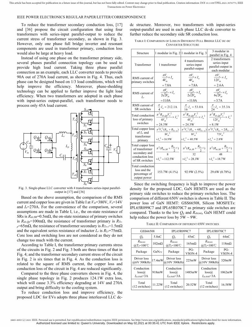
To reduce the transformer secondary conduction loss, [17] and [36] propose the circuit configuration that using four transformers with series-input parallel-output to reduce the current stress of transformer secondary, as shown in Fig. 3. However, only one phase full bridge inverter and resonant components are used in transformer primary, conduction loss would also be large at heavy load.
Instead of using one phase on the transformer primary side, several phases parallel connection topology can be used to provide high load current. Taking three phase parallel connection as an example, each LLC converter needs to provide 90A out of 270A load current, as shown in Fig. 4. Thus, each phase can be designed based on 1/3 load conditions, which will help improve the efficiency. Moreover, phase-shedding technology can be applied to further improve the light load efficiency. When two transformers are adopted in each phase with input-series output-parallel, each transformer needs to process only 45A load current.
Fig. 3. Single-phase LLC converter with 4 transformers series-input parallel-
output in [17] and [36]
Based on the above assumption, the comparison of the RMS current and copper loss are given in Table I at Vin=380V, Vo=14V and Io=270A. For the convenience of the comparison, several assumptions are made in Table I, i.e., the on-state resistance of SRs is Rds,SR=0.5mΩ, the on-state resistance of primary switches is Rds,Qp=100mΩ, the resistance of transformer primary is RTx-
p=65mΩ, the resistance of transformer secondary is RTx-s=1.5mΩ and the equivalent series resistance of inductor Lr is RLr=75mΩ. Core loss and switching loss are not considered as they do not change too much with the current.
According to Table I, the transformer primary currents stress of the circuits in Fig. 2 and Fig. 3 both are three times of that in Fig. 4; and the transformer secondary current stress of the circuit in Fig. 2 is six times that in Fig. 4. As the conduction loss is related to the square of RMS current, the copper loss and conduction loss of the circuit in Fig. 4 are reduced significantly.
Compared to the three phase converters shown in Fig. 4, the single phase topology in Fig. 2 produces 124.1W extra loss, which will cause 3.3% efficiency degrading at 14V and 270A output and bring difficulty to the cooling system.
To reduce conduction loss and improve efficiency, the proposed LDC for EVs adopts three phase interleaved LLC dc-
dc structure. Moreover, two transformers with input-series output-parallel are used in each phase LLC dc-dc converter to further reduce the secondary side SR conduction loss.
TABLE I: COMPARISON OF LOSS IN DIFFERENT FULL BRIDGE LLC DC-DC
CONVERTER STRUCTURE
Structure 1 modular in Fig. 2 1 modular in Fig. 3 3 modular in
parallel in Fig. 4
Transformer 1 transformer 4 transformers
series-input parallel-output
2 transformers series-input
parallel-output in each modular
RMS current of primary switches
4
7.8
oo
in
VI
V
4
7.8
oo
in
VI
V
12
2.6
oo
in
VI
V
RMS current of Lr
2 2
11.0
oo
in
VI
V
2 2
11.0
oo
in
VI
V
6 2
3.7
oo
in
VI
V
RMS current of SR switches
212.14 oI
53.016 oI
35.324 oI
Total conduction loss of primary
switches
2 2, 2
24
24.3W
ds Qp oo
in
R VI
V
2 2, 2
24
24.3W
ds Qp oo
in
R VI
V
2 2, 2
212
8.1W
ds Qp oo
in
R VI
V
Total copper loss of Lr and
transformer primary
2 2
2
2
( )
8
16.9W
o Lr Tx p
in
o
V R R
V
I
2 2
2
2
( 4 )
8
40.5W
o Lr Tx p
in
o
V R R
V
I
2 2
2
2
( 2 )
72
2.8W
o Lr Tx p
in
o
V R R
V
I
Total copper loss of transformer secondary and
conduction loss of SR switches
2,
2
( )2
8
112.5W
Tx sds SR
o
RR
I
2
,
2
( )2
32
28.1W
Tx sds SR
o
RR
I
2
,
2
( )2
48
18.7W
Tx sds SR
o
RR
I
Total conduction loss and the
percentage of output power
153.7W (4.1%) 92.9W (2.5%) 29.6W (0.78%)
Since the switching frequency is high to improve the power density for the proposed LDC, GaN HEMTS are used as the primary side switches to reduce the primary switches loss. The comparison of different 650V switches is shown in Table II. The power loss of GaN HEMT: GSS66508, Silicon MOSFETs: IPL65R099C7 and IPL65R070C7 as primary side switches are compared. Thanks to the low Qg and Rds(on), GaN HEMT could help reduce the power loss by 5W ~ 9W.
TABLE II: COMPARISON OF DIFFERENT 650V SWITCHES
GSS66508 IPL65R099C7 IPL65R070C7
Qg 5.8nC Qg 45nC Qg 64nC
Rds(on) @Tj=100℃
102mΩ Rds(on)
@Tj=100℃ 165mΩ
Rds(on) @Tj=100℃
118mΩ
Package GaNPX Package PG-
VSON-4 Package
PG-VSON-4
Driver loss @6V 500kHz
17.4mW Driver loss
@10V 500kHz 225mW
Driver loss @10V 500kHz
320mW
Conduction loss@
Ids,RMS=3A 918mW
Conduction loss@
Ids,RMS=3A 1485mW
Conduction loss@
Ids,RMS=3A 1062mW
Total (12 switches)
11.22W Total
(12 switches) 20.52W
Total (12 switches)
16.58W
S1
S2
S4
S3
Tx1
Tx2
S5
S6
S8
S7
Tx3
Tx4
Co
Vo
Lr
Cr
Lp
Vin
Cin
Q2
Q4
Q1
Q3
Authorized licensed use limited to: Queen's University. Downloaded on May 02,2021 at 00:35:41 UTC from IEEE Xplore. Restrictions apply.
0885-8993 (c) 2021 IEEE. Personal use is permitted, but republication/redistribution requires IEEE permission. See http://www.ieee.org/publications_standards/publications/rights/index.html for more information.
This article has been accepted for publication in a future issue of this journal, but has not been fully edited. Content may change prior to final publication. Citation information: DOI 10.1109/TPEL.2021.3076773, IEEETransactions on Power Electronics
IEEE POWER ELECTRONICS REGULAR PAPER/LETTER/CORRESPONDENCE
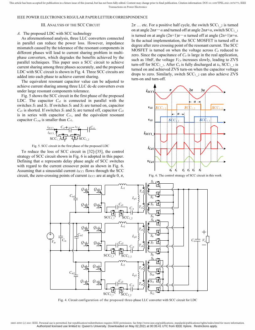
III. ANALYSIS OF THE SCC CIRCUIT
A. The proposed LDC with SCC technology As aforementioned analysis, three LLC converters connected
in parallel can reduce the power loss. However, impedance mismatch caused by the tolerance of the resonant components in different phases will lead to current sharing problem in multi-phase converters, which degrades the benefits achieved by the parallel techniques. This paper uses a SCC circuit to achieve current sharing among three phases accurately, and the proposed LDC with SCC circuit is shown in Fig. 4. Three SCC circuits are added into each phase to achieve current sharing.
The equivalent resonant capacitor value can be adjusted to achieve current sharing among three LLC dc-dc converters even under large resonant components tolerance.
Fig. 5 shows the SCC circuit in the first phase of the proposed LDC. The capacitor Ca1 is connected in parallel with the switches S1 and S2. If switches S1 and S2 are turned on, capacitor Ca1 is shorted. If switches S1 and S2 are turned off, capacitor Ca1 is in series with capacitor Cr1, and the equivalent resonant capacitor Cr,eq is smaller than Cr1.
Fig. 5. SCC circuit in the first phase of the proposed LDC
To reduce the loss of SCC circuit in [32]-[35], the control strategy of SCC circuit shown in Fig. 6 is adopted in this paper. Defining that α represents delay phase angle of SCC switches with regard to the current crossover point as shown in Fig. 6. Assuming that a sinusoidal current iSCC1 flows through the SCC circuit, the zero-crossing points of current iSCC1 are at angle 0, π,
2π … etc. For a positive half cycle, the switch SCC1_2 is turned on at angle 2nπ-α and turned off at angle 2nπ+α, switch SCC1_1 is turned on at angle (2n+1)π-α turned off at angle (2n+1)π+α. In the actual implementation, the SCC MOSFET is turned off α degree after zero crossing point of the resonant current. The SCC MOSFET is turned on when the voltage across Ca reduced to zero. Since the capacitance of Ca is large in the real application, such as 10nF, the voltage VCa increases slowly, leading to ZVS turn-off for SCC1_1. After Ca is fully discharged at t4, SCC1_1 is turned on and achieved ZVS turn-on when the capacitor voltage drops to zero. Similarly, switch SCC1_2 can also achieve ZVS turn-on and turn-off.
Fig. 6. The control strategy of SCC circuit in this work
Fig. 4. Circuit configuration of the proposed three-phase LLC converter with SCC circuit for LDC
Ca1
SCC1_1 SCC1_2
iCa1 Cr1iSCC1
iSCC1_1
iCa1
SCC1_1vGS
vCa1
iSCC1
α
π 2π 3π
SCC1_2vGS
α
t0 t1 t2 t3 t4 t5
SCC1_2 SCC1_2
SCC1_1
iSCC1_1
Cin1
Lr1
Cr1
Q1
Q3
Lp1
Co Vo
S1
S2
Q2
Q4
S4
Vin
Lr2
Cr2
Q5
Q7
Lp2
S5
S6
Q6
Q8
S8
Lr3
Cr3
Q9
Q11
Lp3
S9
S10
Q10
Q12
S12
S11
S7
S3Ca1
SCC1_1 SCC1_2
SCC2_1 SCC2_2
SCC3_1 SCC3_2
Ca2
Ca3
Tx1
Tx2
Tx3
Tx4
Tx5
Tx6
Cin2
Cin3
Cin
Authorized licensed use limited to: Queen's University. Downloaded on May 02,2021 at 00:35:41 UTC from IEEE Xplore. Restrictions apply.
0885-8993 (c) 2021 IEEE. Personal use is permitted, but republication/redistribution requires IEEE permission. See http://www.ieee.org/publications_standards/publications/rights/index.html for more information.
This article has been accepted for publication in a future issue of this journal, but has not been fully edited. Content may change prior to final publication. Citation information: DOI 10.1109/TPEL.2021.3076773, IEEETransactions on Power Electronics
IEEE POWER ELECTRONICS REGULAR PAPER/LETTER/CORRESPONDENCE
Taking the first phase circuit as an example, from [31], the equivalent capacitance of SCC circuit can be calculated as
1
, 1 .2 (2 sin2 ) /
aSCC phase
CC
(1)
From Fig. 5 and (1), the equivalent resonant capacitor Cr,eq is
, 1 1,
, 1 1
.SCC phase rr eq
SCC phase r
C CC
C C
(2)
Taking SCC circuit into consideration, the voltage gain of the first phase circuit in the proposed LDC becomes
2 212 2 2 2
4 2
2,
( )[( ) 1] [( ) 1]
64
o
in s pr r
s sL
nV KM
V LK
n R
(3)
where RL is load resistance of the first phase, K=Lp1/Lr1,
ωs=2πfs, and ωr=1/ 1 , .r r eqL C Similarly, the second and third
phase have the same voltage gain shown in (3) when the same resonant parameters are selected.
In LLC dc-dc converter, the resonant components parameters are always designed with the assumption that there is no tolerance among multi phases circuits. According to (1) and (2), a large α has small effect on the resonant parameters of LLC converter. Therefore, in the proposed LDC, delay angles of all three phases SCC switches α are set to the maximum value αmax at the beginning. If there is tolerance among three phases, SCC circuit will compensate the resonant parameters and make three phase current sharing by adjusting α.
From (3), the load currents of three phases can be shared by adjusting the delay angle α of switches SCC1_1~ SCC3_2 so that three phase circuits have the same voltage gains at the same switching frequency. Therefore, the total input current and load current will be distributed into three phases equally even if the three phase converters have large resonant components tolerance.
B. Loss analysis of SCC circuit
In the SCC circuit, from Fig. 6, the RMS current flowing through SCC switches ISCC1_1,RMS is
2
1_1,
1,
1,
2 sin( )
2 sin21
Lr RMS
Lr RMS
SCC RMS
t dtI
I
I
. (4)
The average absolute value of the current flowing through SCC switches ISCC1_1, AVE_ABS is
1_1 _
, 1,,
12 sin( ) 2 2cosSCC AVE A
Lr RMS L RMS
rB
St d
II It
.
(5)
As ZVS turn-on and turn-off are achieved, there is only conduction loss of two SCC switches. The current iSCC1_1 flows through one MOSFET and one body diode of MOSFET in the control strategy of [32]-[35], thus the loss of one SCC circuit in [32]-[35] is
2
1_1, ( ) 1_1, _
1
, 32 35
2), (1
2 ,2 22 sin2( 1) cos
SCC RMS ds on SCC AVE ABS Floss
Lr RMSLr R
SCC in
Fds oMS n
P I R I V
IV
RI
.(6)
From Fig. 5 and Fig. 6, current iSCC1_1 flows through two MOSFETs in this work, thus the loss of one SCC circuit in the proposed LDC is
2, (
1,
) 1_1,
2 2( )
2
2 sin22 ( 1)
loss SCC in this work ds on SCC RMS
ds oLr RMS nI
P R I
R
. (7)
According to (6) and (7), the loss of one SCC circuit against delay angle α with different resonant current ILr1,RMS in [32]-[35] and in this work is shown in Fig. 7. As three SCC circuits are used in the proposed LDC, if ILr1,RMS=4A and α=160°, the total loss of three SCC switches is 11.1W in [32]-[35], while the total loss of three SCC switches is only 1.9W in this work, which can help reduce the power loss by 9.2W.
Fig. 7. Loss comparison of the SCC circuit
IV. PARAMETERS DESIGN OF THE LDC
Since the three phase LLC dc-dc converters have the same parameters design in the proposed LDC, only taking the first phase circuit analysis as an example. To ensure the converter operates in the ZVS region of primary switches and ZCS region of the SR, the resonant point (unity voltage gain) is selected based on the maximum input voltage and the minimum output voltage. The transformer turns ratio is determined by
_ _: :p s in max o minn N N V V (8)
where, Np is the primary turns number and Ns is the secondary turns number.
With 430V maximum input and 9V minimum output voltage, each transformer turns ratio should be 430V / 9V / 2 = 23.8. However, as 9V is an odd point with less current requirement, the turns ratio is selected as 22:1:1 for each transformer.
For EVs, the maximum output power of the LDC is limited by the voltages across high voltage battery. In this case, load capacity is different at different input and output conditions. Each phase of the LLC dc-dc converter considers maximum 90A
Plo
ss
(W)
α (°)
ILr,RMS=6A
ILr,RMS=4A
ILr,RMS=2A
} }
SCC loss in this work
SCC loss in [32]-[35]
Authorized licensed use limited to: Queen's University. Downloaded on May 02,2021 at 00:35:41 UTC from IEEE Xplore. Restrictions apply.

0885-8993 (c) 2021 IEEE. Personal use is permitted, but republication/redistribution requires IEEE permission. See http://www.ieee.org/publications_standards/publications/rights/index.html for more information.
This article has been accepted for publication in a future issue of this journal, but has not been fully edited. Content may change prior to final publication. Citation information: DOI 10.1109/TPEL.2021.3076773, IEEETransactions on Power Electronics
IEEE POWER ELECTRONICS REGULAR PAPER/LETTER/CORRESPONDENCE
×14V=1260W load for resonant parameter design. For 330V to 430V input voltage, the converter is rated for full power; while for 250V to 330V input voltage, only 60% load is needed. In the proposed LDC, wide input voltage (250V~430V) and output voltage (9V~16V) range are required. Because 250V input and 16V output is maximum step-up voltage gain point, the design of the resonant parameters should satisfy this condition. As only 60% load is needed at 250V input voltage, voltage gain should satisfy
Case 1: 16 44
2.82,250
o
in
nVM
V
(9)
in this case, for each phase, quality factor Q satisfies
2 21 1
2 21 1
3 1
1
/ 3 (90 0.6 14 16)
8 8 44 16
1.882 10 .
o r r
r ro
r
r
I L LQ
C Cn V
L
C
(10)
When the input voltage is 330V, full load needs to be carried, and the resonant parameters should be designed for this condition. When the output voltage is 16V, the maximum step-up voltage gain is
Case 2: 16 44
2.13,330
o
in
nVM
V
(11)
and quality factor Q satisfies
2 21 1
2 21 1
3 1
1
/ 3 (90 14 16)
8 8 44 16
3.136 10 .
o r r
r ro
r
r
I L LQ
C Cn V
L
C
(12)
As large Q value would decrease voltage gain, 14V output 90A load current should also be considered in this design. When the output voltage is 14V, the maximum step-up voltage gain is
Case 3: 14 44
1.87,330
o
in
nVM
V
(13)
and quality factor Q satisfies
2 21 1
2 21 1
3 1
1
/ 3 90
8 8 44 14
4.097 10 .
o r r
r ro
r
r
I L LQ
C Cn V
L
C
(14)
Compared with 100kHz~200kHz resonant frequency in traditional LDC, the resonant frequency between Lr1 and Cr1 is selected to be around 500kHz to reduce the volume of magnetic components and improve the power-density in this work. According to [38], three sets of resonant parameters are selected to meet the parameters design for the proposed LDC, and the accurate voltage gain curves are given in Fig. 8 by using time-domain analysis method.
As shown in Fig. 8(a), when K=3, fr=546kHz, Q=0.45, that is Lr1=32uH, Lp1=96uH and Cr1=2.7nF, the maximum voltage gains of the three cases are achievable, and the minimum switching frequency is 0.58fr. However, the inductance of Lp is
too small, which is difficult to optimize the fringing loss and core loss. As shown in Fig. 8(b), when K=5, fr=546kHz, Q=0.35, that is Lr1=25uH, Lp1=125uH and Cr1=3.4nF, the maximum voltage gains of the three cases are also achievable, and the minimum switching frequency is 0.47fr. As shown in Fig. 8(c), when K=8, fr=546kHz, Q=0.25, that is Lr1=18uH, Lp1=142uH and Cr1=4.8nF, the maximum voltage gains of the three cases can also be achieved, and the minimum switching frequency is smaller than 0.4fr.
(a) voltage gain when K=3, Q=0.45 (Lr1=32μH, Lp1=96μH,
Cr1=2.7nF)
(b) voltage gain when K=5, Q=0.35 (Lr1=25μH, Lp1=125μH,
Cr1=3.4nF)
(c) voltage gain when K=8, Q=0.25 (Lr1=18μH, Lp1=142μH,
Cr1=4.8nF)
Fig. 8. Voltage gain with different resonant parameters
If the switching frequency is too far away from the resonant frequency, the efficiency of the converter would not be optimal. As Lp1 is too small in the first set of resonant parameters and the switching frequency range is too wide in the third set of resonant
Authorized licensed use limited to: Queen's University. Downloaded on May 02,2021 at 00:35:41 UTC from IEEE Xplore. Restrictions apply.

0885-8993 (c) 2021 IEEE. Personal use is permitted, but republication/redistribution requires IEEE permission. See http://www.ieee.org/publications_standards/publications/rights/index.html for more information.
This article has been accepted for publication in a future issue of this journal, but has not been fully edited. Content may change prior to final publication. Citation information: DOI 10.1109/TPEL.2021.3076773, IEEETransactions on Power Electronics
IEEE POWER ELECTRONICS REGULAR PAPER/LETTER/CORRESPONDENCE
parameters, the second set of resonant parameters Lr1=25μH, Lp1=125μH, Cr1=3.4nF are selected, and the resonant parameters of the second and third phase are the same as that of the first phase.
V. MAGNETIC COMPONENTS AND PCB DESIGN OF THE
PROPOSED LDC
A. Design of magnetic components
In this work, the center-tap transformer is used with 22:1:1 turns ratio. As shown in Fig. 4, two transformers primary are in series, if Lp1 is selected as 125μH, 62.5μH magnetizing inductor is needed in each transformer. As at least 22 turns are designed for transformer primary winding, thus a large air gap is required for the transformers, which means large fringing loss. In the proposed LDC, an external inductor Lp1 is used so that no air gap is needed for the transformer to improve the efficiency.
If the proposed LDC operates at resonant frequency with 380V input and 14V/270A output, the RMS current flowing through one of the transformer secondary side winding is
1, ,/ 3 1
35.32 2 2 2
oTx s RMS
Ii
, (15)
the RMS current of transformer primary winding is
1, ,1, ,
22.3Tx s RMS
Tx p RMS
ii
n , (16)
the RMS current iLp1 is
1,1
2 11.3
4 3o
Lp RMSp
nV Ti
L , (17)
and the RMS current iLr1 is
1,/ 3
3.72 2
o oLr RMS
in
V Ii
V
. (18)
As the converter operates at a switching frequency higher than 260kHz, Litz wire is used to implement the magnetic components to reduce the AC losses caused by skin effect and proximity effect.
According to the current stress shown in (15) - (18), the different litz wires are selected for the magnetic components. The core size, material and structure of all the magnetic components are shown in Table III.
TABLE III: CORE SIZE AND MATERIAL OF MAGNETIC COMPONENTS
Inductor Lr1 Inductor Lp1 Transformer
Core Size PQ32/20 Core Size PQ35/35 Core Size PQ35/35
Material 3C97 Material 3C97 Material 3C97
Litz Wire NELC650
/44SN Litz Wire
NELC1100/48SN
Litz Wire / Copper
foil
NELC650/44SN / three-layer laminated 0.25mm copper foil
Turns 15 Turns 44 Turns 22:1:1
Laminated layers
3 Laminated
layers 4
Laminated layers
2 (Primary) / 3 (Secondary)
Air gap 1.5mm Air gap 5mm Air gap 0mm
Fig. 9 shows the photo of the primary side and secondary side of the transformer. The primary winding uses 22 turns of 2 layers of litz wire. On the secondary side, each of the center-tapped
windings is created using 1 turn of three paralleled 20mm × 0.25mm copper foils.
(a) primary side (b) secondary side Fig. 9. Photo of the transformer
B. Design of PCB board
For the LDC prototype, if only one PCB board is used, magnetic components, controller circuit and active devices should be placed on the same one board. Thus, the vertical space of the structure is not efficiently used because the height of magnetic components is much larger than controller circuit and active devices. The space above the active devices and controller circuit is basically not utilized, which reduces the power density of the converter.
(a) Top view of the LDC
(b) Front view of the LDC with two PCB liquid cooling assembly
Fig. 10. 3D Model of the proposed LDC
Fig. 10 shows the 3D model of the proposed LDC. A two-PCB structure is proposed to make full use of the vertical space. The upper PCB is the controller board. MCU, gate driver of switches etc, are placed on this board. The lower PCB is the power board. Primary GaN HEMTs, SCC switches and SR switches are placed on this board. Between the two parallel PCBs, a short distance is designed to place the devices. Magnetic components are placed on top of the control board (top board). The pins of the magnetic components are connected to the power board (bottom board) by metal connectors. The liquid cooling cold plate is connected to the bottom side of the power PCB to maximize the cooling performance on active devices to dissipate heat. Thus, high power-density is achieved in this design.
Authorized licensed use limited to: Queen's University. Downloaded on May 02,2021 at 00:35:41 UTC from IEEE Xplore. Restrictions apply.

0885-8993 (c) 2021 IEEE. Personal use is permitted, but republication/redistribution requires IEEE permission. See http://www.ieee.org/publications_standards/publications/rights/index.html for more information.
This article has been accepted for publication in a future issue of this journal, but has not been fully edited. Content may change prior to final publication. Citation information: DOI 10.1109/TPEL.2021.3076773, IEEETransactions on Power Electronics
IEEE POWER ELECTRONICS REGULAR PAPER/LETTER/CORRESPONDENCE
VI. EXPERIMENTAL RESULTS
To verify the analysis, a 3.8kW LDC prototype is built and tested. The series resonant inductor is 25μH, the parallel inductor is 125μH, the resonant capacitor is 3.4nF, the SCC capacitor is 14nF and the transformer turns ratio is np:ns1:ns2=22:1:1. The specifications and parameters of the proposed LDC are given in Table IV.
TABLE IV: SPECIFICATIONS AND PARAMETERS OF THE PROPOSED LDC
Input voltage 250V ~ 430V Output voltage 9V ~ 16V
Maximum output current
270A (90A×3)
Maximum output power
3.8kW
Transformer Np:Ns = 22 : 1, PQ35/35 core
Parallel inductor Lp1 = 125.3µH, Lp2 =124.3µH, Lp3 = 124.5µH,
PQ35/35 core
Series inductor Lr1 = 25.6µH, Lr2 = 25.7µH, Lr3 = 25µH,
PQ32/20 core Series capacitor C1808C681JGGAC7800 2KV, 680pF ×5 (±5%) SCC capacitor C2012NP02W472J125AA, 450V, 4700 pF × 3
Primary switches GS66508B (650V, 30A) Secondary switches TPHR8504PL (40V, 150A)
SCC switches IPB200N25N3 (250V, 64A)
Input capacitor C5750X6S2W225K250KA, 450V, 2.2µF × 18
+ UPZ2W560MHD, 450V, 56µF × 1
Output capacitor C3216JB1E336M160AC, 25V, 33µF × 10
+ UHE1E331MPD, 25V, 330µF × 2 Micro-controller DSPIC33FJ32GS610
Fig. 11 and 12 show the prototype of the proposed LDC and the test bench. The prototype with 3kW/L power-density and 1.5kg weight is achieved. In the proposed LDC, three interleaved LLC converters are paralleled for reducing the current stress to improve the efficiency, and the SCC circuit is used to make sure three phase current sharing. The liquid cooling is used for heat dissipation of the devices on the main board, and the fan cooling is used for heat dissipation of the magnetic components. Three 90A electronics load is paralleled to provide 270A load. In practice, the highest current tested is 260A due to the power limitation of the electronic load.
Fig. 11. Prototype of the proposed LDC
As shown in Fig. 13, a wide voltage range 250V~430V input and 9V~16V output is achieved. In Fig. 13(a), input and output voltages are 430V and 14V with 5A load current, and the switching frequency is 324kHz. In Fig. 13 (b), input and output voltages are 250V and 16V with 40A load current, and the switching frequency is 260kHz. In Fig. 13(c), input and output voltages are 330V and 9V with 70A load current, and the switching frequency is 346kHz. From Fig. 13, ZVS turn-on can
be achieved in light and heavy load at a wide switching frequency range.
Fig. 12. The test bench
(a) at 430V input and 14V output with 5A load current
(b) at 250V input and 16V output with 40A load current
(c) at 330V input and 9V output with 70A load current
Fig. 13. Waveforms of vgs, vds of primary switches and current iLr, iLp in single phase circuit
As shown in Fig. 14, input and output voltage are 380V and 14V when the load of the second phase circuit is 90A, delay angle α is 149°. From Fig. 14, ZVS turn-on and ZVS turn-off can be achieved, and the voltage stress of the switches in SCC circuit is low (around 25V), which verifies the analysis.
Authorized licensed use limited to: Queen's University. Downloaded on May 02,2021 at 00:35:41 UTC from IEEE Xplore. Restrictions apply.

0885-8993 (c) 2021 IEEE. Personal use is permitted, but republication/redistribution requires IEEE permission. See http://www.ieee.org/publications_standards/publications/rights/index.html for more information.
This article has been accepted for publication in a future issue of this journal, but has not been fully edited. Content may change prior to final publication. Citation information: DOI 10.1109/TPEL.2021.3076773, IEEETransactions on Power Electronics
IEEE POWER ELECTRONICS REGULAR PAPER/LETTER/CORRESPONDENCE
Fig. 14. Waveform of the second phase SCC circuit at 380V input and
14V/90A output
(a) SCC capacitor voltage vCa2 and vCa3
(b) the resonant current iLr2 and iLr3
Fig. 15. Waveforms of two-phase circuits operation at 250V input,
14V/100A output
Fig. 15 shows the waveforms of the SCC current sharing technology is used in the proposed LDC. When the second and third phase circuits operate at 250V input and 14V output voltage with 100A load current, switching frequency is 269kHz and the delay angles α are 148° and 135° respectively in the second and third phase SCC circuits. Two resonant currents iLr2 and iLr3 are very closely balanced by adjusting the delay angle α in the two SCC circuits.
As shown in Fig. 16, when the three-phase circuits of the proposed LDC operate at 380V input and 14V output voltage with 200A load current, switching frequency is 311kHz and the delay angles α are 144°, 150° and 132° respectively in the three SCC circuits. Fig. 17 shows the waveforms when input is 380V and output is 14V / 260A with three-phase operation. The switching frequency is 305kHz and the delay angles α are 136°, 154° and 126° respectively in the three SCC circuits. From Fig. 16 and 17, the resonant currents of the three phase LLC dc-dc
converters are balanced well by adjusting the delay angle α under different operation conditions.
(a) SCC capacitor voltage vCa1, vCa2 and vCa3
(b) the resonant current iLr1, iLr2 and iLr3
Fig. 16. Waveforms of three-phase circuits operation at 380V input, 14V/200A output
(a) SCC capacitor voltage vCa1, vCa2 and vCa3
(b) the resonant current iLr1, iLr2 and iLr3
Fig. 17. Waveforms of three-phase circuits operation at 380V input, 14V/260A output
Authorized licensed use limited to: Queen's University. Downloaded on May 02,2021 at 00:35:41 UTC from IEEE Xplore. Restrictions apply.

0885-8993 (c) 2021 IEEE. Personal use is permitted, but republication/redistribution requires IEEE permission. See http://www.ieee.org/publications_standards/publications/rights/index.html for more information.
This article has been accepted for publication in a future issue of this journal, but has not been fully edited. Content may change prior to final publication. Citation information: DOI 10.1109/TPEL.2021.3076773, IEEETransactions on Power Electronics
IEEE POWER ELECTRONICS REGULAR PAPER/LETTER/CORRESPONDENCE
Fig. 18. RMS resonant current iLr1, iLr2 and iLr3 at 380V input 14V output with
three-phase circuits operation
Fig. 18 shows RMS resonant current at 380V input 14V output with three-phase circuits operation. When load current increases from 140A to 260A, the current sharing error σresonant is always smaller than 2.5%, which means three phase load currents are very balanced.
Power loss breakdown is given in Fig. 19. In this paper, the optimal SR conduction time is not concerned as there are many methods to optimize the SR conduction time [10], [39]. In the proposed LDC, NCP4305 synchronous rectifier chip is used and constant conduction time 0.825us of SR switches is adopted. If SR conduction time is optimized, the body diode loss of S1~S12 could be removed, and the efficiency can be improved further.
Fig. 20 shows the efficiency of single phase, two phase and three phase circuits at 380V input and 14V output. Phase shedding is used to achieve the highest efficiency for each load range. When the input voltage is 380V, single phase circuit operates at from 0A load current to 80A load current, two phase circuits operate from 80A load current to 130A load current and three phase circuits operate from 130A load current to 260A load current.
Fig. 21 shows the efficiency curves of the proposed LDC at different input voltage and 14V output voltage. 95% and higher efficiency can be achieved over the wide load ranges (from 20A load to full load). When the input voltage is 380V and output voltage is 14V, 95.8% efficiency is achieved at 260A load current, and peak efficiency is 96.7%.
Fig. 22 shows the thermal images at 380V input, 14V/260A output with 25°C fluid liquid cooling and fan cooling, and the temperature is lower than 80℃.
(a) the power loss distribution at full load
(b) the power loss distribution at half load
Fig. 19. Loss breakdown of the proposed LDC
Fig. 20. The efficiency of single phase, two phase and three phase circuits at 380V input and 14V output
Fig. 21. The efficiency of the proposed LDC when the output voltage is 14V
The performance of EV LDC as presented in recent literatures [1]-[8], [14]-[17], [45]-[46] and the products [40]-[44] is summarized in Table V for a comprehensive comparison. It shows that with SCC technology, the LDC designed in this paper achieves high efficiency and high power-density at the same time.
(a) Input terminal (b) Output terminal
Fig. 22. Thermal images at 380V input, 14V/260A output with 25°C fluid liquid cooling and fan cooling
0%
1%
2%
3%
4%
5%
6%
0.0
0.5
1.0
1.5
2.0
2.5
3.0
3.5
4.0
4.5
140A 150A 160A 170A 180A 190A 200A 210A 220A 230A 240A 250A 260A
Phase 1 Phase 2 Phase 3 Current sharing error
Iout (A)
Resonant currents of SCC-LLC converter @ Vo=14V Vin=380V
Res
onan
t cur
rent
(A
)
20 40 60 80 100 120 140 160 180 200 220 240 260Single phase 95.3% 96.3% 96.4% 96.1%Two phase 96.1% 96.4% 96.4% 96.4%Three phase 96.5% 96.5% 96.3% 96.3% 96.1% 95.9% 95.8%
93.0%
94.0%
95.0%
96.0%
97.0%
Single phase Two phase Three phase
Iout (A)
Efficiency of the prototype @ Vin=380V, Vo=14V
Eff
icie
ncy
(%)
20 40 60 80 100 120 140 160 180 200 220 240 260380V input 95.3% 96.3% 96.4% 96.1% 96.4% 96.4% 96.4% 96.5% 96.3% 96.3% 96.1% 95.9% 95.8%330V input 95.3% 96.6% 96.3% 96.3% 96.3% 96.6% 96.7% 96.7% 96.4% 96.2% 96.0% 95.7% 95.4%250V input 94.9% 96.5% 96.1% 96.5% 96.4% 96.3% 96.2% 96.1%
93.0%
94.0%
95.0%
96.0%
97.0%
380V input 330V input 250V input
Iout (A)
Efficiency of the prototype @ Vo=14V
Eff
icie
ncy
(%)
Authorized licensed use limited to: Queen's University. Downloaded on May 02,2021 at 00:35:41 UTC from IEEE Xplore. Restrictions apply.

0885-8993 (c) 2021 IEEE. Personal use is permitted, but republication/redistribution requires IEEE permission. See http://www.ieee.org/publications_standards/publications/rights/index.html for more information.
This article has been accepted for publication in a future issue of this journal, but has not been fully edited. Content may change prior to final publication. Citation information: DOI 10.1109/TPEL.2021.3076773, IEEETransactions on Power Electronics
IEEE POWER ELECTRONICS REGULAR PAPER/LETTER/CORRESPONDENCE
TABLE V: COMPARISON BETWEEN THE PROPOSED LDC AND OTHERS LDC
Reference Specification of the Converter
Topology Configuration Input voltage Output voltage
Rated power
Peak efficiency
Full-load efficiency
Rated power density
Switching frequency
[1] Phase-shift full bridge converter
1 module 200V~400V 12V 1.2kW 95.5% 90% 0.5kW/L 100kHz
[2] Phase-shift full bridge converter
1 module 300V 12V 2kW 94% 93.2% - 227kHz
~297kHz
[3] Phase-shift full bridge converter
1 module 235V~431V 11.5V~15V 2kW 93.5% 93% 0.94kW/L 200kHz
[4] Phase-shift full bridge converter
1 module 300V~400V 12V~16V 0.7kW 93.5% 90% - 100kHz
[5] Phase-shift full bridge converter
1 module 250V~400V 13V~15V 1kW 93% 92% - 100kHz
[6] Phase-shift full bridge converter
3 modules in parallel
300V 14V 1.2kW 94.7% 93.9% - 100kHz
[7] Three-level phase-
shift half bridge converter
1 module 200V 12V 0.5kW 91% 90% 40kHz
[8] Two-stage converters
2 modules in parallel
200V~400V 12V 2kW 95.9% 94.3% - 100kHz
~133kHz
[14] LLC converter 1 module 220V~450V 6.5V~16V 2.5kW 93.2% 92% 1.17kW/L 90kHz
~200kHz
[15] LLC converter 1 module 260V~430V 12.5V~14.5V 1.9kW 93% 91% 1.02kW/L 65kHz
~150kHz
[16] LLC converter 2 modules in
parallel 330V~410V 14V 2.5kW 95% 93% 1kW/L 250kHz
[17] LLC converter 1 module 300V~430V 12V 3kW 94% 93% 21.4kW/L 320kHz
~500kHz
[40] - - 250V~420V 12V~13.5V 2kW 90% - 0.26kW/L -
[41] - - 180V~450V 9V~16V 3kW 94% 92% 0.53kW/L -
[42] Buck-Boost
converter+Series resonant converter
1 module 220V~450V 8V~16V 3.5kW 93.5% - 1.11kW/L 40kHz
~150kHz
[43] - - 240V~430V 9V~16V 4kW 93% 92% 0.38kW/L -
[44] - - 250V~425V 13.8V 2.4kW 82% - 0.6kW/L -
[45] Buck converter
+LLC DCX 1 module 250V~450V 10V~16V 3.5kW 96% 92% 1.3kW/L 200kHz
[46] Phase-shift full bridge converter
1 module 200V~310V 12.8V~15.1V 1.8kW 91.9% 90% 8.1kW/L 700kHz
The proposed LDC
SCC-LLC converter
3 modules in parallel
250V~430V 9V~16V 3.8kW 96.7% 95.8% 3kW/L 260kHz
~400kHz
VII. CONCLUSION
To reduce the conduction loss at high load current, three phase interleaved LLC dc-dc converters in parallel are designed for EV LDC in this paper. SCC circuit is added into resonant tank to achieve current sharing among three phases. In the proposed LDC, GaN HEMTs are used in transformer primary side, allowing the switching frequency to be increased while the volume of the circuit is reduced. ZVS turn-on of the primary switches and ZCS turn-off of secondary SRs are achieved. ZVS operation and low conduction loss of the SCC circuit switches are also achieved. By adjusting the delay angle α of SCC, three phase resonant currents are balanced. Two PCB board structure and the liquid cooling cold plate are designed to improve the power-density and limit the temperature rise. The proposed LDC achieves an efficiency of 95.8% at 260A load current and a peak
efficiency of 96.7% with a 3kW/L power-density. Phase shedding is used for different load currents, which results in high efficiency over the full load range. Compare with others LDC, the proposed LDC achieves both high efficiency and high power-density simultaneously.
REFERENCES [1] Ruoyu Hou and Ali Emadi, “Applied integrated active filter auxiliary
power module for electrified vehicles with single-phase onboard chargers,” IEEE Transactions on Power Electronics., vol. 32, no. 3, pp. 1860-1871, Mar. 2017.
[2] Majid Pahlevaninezhad, Josef Drobnik, Praveen K. Jain and Alireza Bakhshai, “A load adaptive control approach for a zero-voltage-switching dc/dc converter used for electric vehicles,” IEEE Transactions on Industrial Electronics., vol. 59, no. 2, pp. 920-933, Feb. 2012.
[3] Djilali Hamza, Majid Pahlevaninezhad, and Praveen K. Jain, “Implementation of a novel digital active EMI technique in a DSP-based
Authorized licensed use limited to: Queen's University. Downloaded on May 02,2021 at 00:35:41 UTC from IEEE Xplore. Restrictions apply.
0885-8993 (c) 2021 IEEE. Personal use is permitted, but republication/redistribution requires IEEE permission. See http://www.ieee.org/publications_standards/publications/rights/index.html for more information.
This article has been accepted for publication in a future issue of this journal, but has not been fully edited. Content may change prior to final publication. Citation information: DOI 10.1109/TPEL.2021.3076773, IEEETransactions on Power Electronics
IEEE POWER ELECTRONICS REGULAR PAPER/LETTER/CORRESPONDENCE
dc–dc digital controller used in electric vehicle (EV),” IEEE Transactions on Power Electronics., vol. 28, no. 7, pp. 3126-3137, Jul. 2013.
[4] Ruoyu Hou and Ali Emadi, “A primary full-integrated active filter auxiliary power module in electrified vehicles with single-phase onboard chargers,” IEEE Transactions on Power Electronics., vol. 32, no. 11, pp. 8393-8405, Nov. 2017.
[5] Yun-Sung Kim, Chang-Yeol Oh, Won-Yong Sung and Byoung Kuk Lee, “Topology and control scheme of OBC–LDC integrated power unit for electric vehicles,” IEEE Transactions on Power Electronics., vol. 32, no. 3, pp. 1731-1743, Mar. 2017.
[6] Khairy Sayed, “Zero-voltage soft-switching dc–dc converter-based charger for LV battery in hybrid electric vehicles,” IET Power Electronics., vol. 12, no. 13, pp. 3389-3396, 2019.
[7] Hyun-Bin Kim and Jong-Soo Kim, “Implement of high efficiency achievement algorithm of LDC for xEV based on GaN HEMT,” IEEE Transportation Electrification Conference and Expo, Asia-Pacific (ITEC Asia-Pacific), 2019.
[8] Dongok Moon, Junsung Park and Sewan Choi, “New interleaved current-fed resonant converter with significantly reduced high current side output filter for EV and HEV applications,” IEEE Transactions on Power Electronics., vol. 30, no. 8, pp. 4264-4271, Aug. 2015.
[9] Bo Yang, Fred C. Lee, A.J. Zhang and Guisong Huang, “LLC resonant converter for front end dc/dc conversion,” in Proc. IEEE 17th Annu. Appl. Power Electron. Conf. Expo., 2002, vol. 2, pp. 1108–1112.
[10] Dianbo Fu, Bing Lu, and Fred C. Lee, “1 MHz high efficiency LLC resonant converters with synchronous rectifier,” in Proc. Power Electron. Spec. Conf., 2007, pp. 2404–2410.
[11] Zhiliang Zhang, Ya-Qi Wu, Dong-Jie Gu and Qianhong Chen, “Current ripple mechanism with quantization in digital LLC converters for battery charging applications,” IEEE Trans. Power Electron., vol. 33, no. 2, pp. 1303–1312, Feb. 2018.
[12] Haoran Li, Zhiliang Zhang, Shengdong Wang, Jiacheng Tang, Xiaoyong Ren and Qianhong Chen, “A 300-kHz 6.6-kW SiC bidirectional LLC onboard charger,” IEEE Transactions on Industrial Electronics., vol. 67, no. 2, pp. 1435–1445, Feb. 2020.
[13] Zhiliang Zhang, Zhi-Wei Xu, Haoran Li, Mingxie He, Jiachen Tang, Xiaoyong Ren and Qianhong Chen, “A 1-kV input SiC LLC converter with split resonant tanks and matrix transformers,” IEEE Transactions on Power Electronics., vol. 34, no. 11, pp. 10446 - 10457, Nov. 2019.
[14] Chen Duan, Hua Bai, Wei Guo and Zhong Nie, “Design of a 2.5-kW 400/12V high-efficiency dc/dc converter using a novel synchronous rectification control for electric vehicles,” IEEE Transactions on Transportation Electrification., vol. 1, no. 1, pp. 106-114, Jun. 2015.
[15] Dong-Hee Kim, Min-Jung Kim and Byoung-Kuk Lee, “An integrated battery charger with high power density and efficiency for electric vehicles,” IEEE Transactions on Power Electronics., vol. 32, no. 6, pp. 4553-4565, Jun. 2017.
[16] Gang Yang, Patrick Dubus, and Daniel Sadarnac, “Double-phase high-efficiency, wide load range high-voltage/low-voltage LLC dc/dc converter for electric/hybrid vehicles,” IEEE Transactions on Power Electronics., vol. 30, no. 4, pp. 1876-1886, Apr. 2015.
[17] G. C. Knabben, J. Schafer, J. W. Kolar, G. Zulauf, M. J. Kasper and G. Deboy, “Wide-input-voltage-range 3 kW dc-dc converter with hybrid LLC & boundary/discontinuous mode control,” 2020 IEEE Applied Power Electronics Conference and Exposition - APEC 2020, pp. 1359-1366, 17-21 March 2020.
[18] Hui Chen, Xinke Wu and Shuai Shao, “A current-sharing method for interleaved high frequency LLC converter with partial energy processing,” IEEE Transactions on Industrial Electronics., vol. 67, no. 2, pp. 1498–1507, Feb. 2020.
[19] Hongfei Wu, Xiaohai Zhan and Yan Xing, “Interleaved LLC resonant converter with hybrid rectifier and variable-frequency plus phase-shift control for wide output voltage range applications,” IEEE Transactions on Power Electronics., vol. 32, no. 6, pp. 4246-4257, Jun. 2017.
[20] Mengxi Li, Hongfei Wu, Chengzhi Qu, Yuhui Ji, Yangjun Lu, Yan Xing, Kai Sun, “Ultra-wide output voltage range dc power supply with multiple power modules series/parallel variable structure and automatic voltage/current sharing,” IEEE Energy Conversion Congress and Exposition (ECCE)., pp. 5935-5940, 2019.
[21] Chao Fei, Rimon Gadelrab, Qiang Li and Fred C. Lee, “High-frequency three-phase interleaved LLC resonant converter with GaN devices and integrated planar magnetics,” IEEE Journal of Emerging and Selected Topics in Power Electronics., vol. 7, no. 2, pp. 653-663, Jun. 2019.
[22] Sayed Abbas Arshadi, Martin Ordonez, Wilson Eberle, Mohammad Ali Saket, Marian Craciun and Chris Botting, “Unbalanced three-phase LLC resonant converters: analysis and trigonometric current balancing,” IEEE Transactions on Power Electronics., vol. 34, no. 3, pp. 2025-2038, Mar. 2019.
[23] Ho-Sung Kim, Ju-Won Baek, Myung-Hyu Ryu, Jong-Hyun Kim and Jee-Hoon Jung, “The high-efficiency isolated ac–dc converter using the three-phase interleaved LLC resonant converter employing the Y-connected rectifier,” IEEE Transactions on Power Electronics., vol. 29, no. 8, pp. 4017-4028, Aug. 2014.
[24] Hongliang Wang, Yang Chen, Yajie Qiu, Peng Fang, Yan Zhang, Laili Wang, Yan-Fei Liu, Jahangir Afsharian and Zhihua (Alex) Yang, “Common capacitor multiphase LLC converter with passive current sharing ability,” IEEE Transactions on Power Electronics., vol. 33, no. 1, pp. 370-387, Jan. 2018.
[25] Hongliang Wang, Yang Chen and Yan-Fei Liu, “A passive-impedance-matching technology to achieve automatic current sharing for a multiphase resonant converter,” IEEE Transactions on Power Electronics., vol. 32, no. 12, pp. 9191-9209, Dec. 2017.
[26] Hongliang Wang, Yang Chen, Yan-Fei Liu, Jahangir Afsharian and Zhihua Yang, “A passive current sharing method with common inductor multiphase LLC resonant converter,” IEEE Transactions on Power Electronics., vol. 32, no. 9, pp. 6994-7010, Sep. 2017.
[27] Or Kirshenboim and Mor Mordechai Peretz, “Combined multilevel and two-phase interleaved LLC converter with enhanced power processing characteristics and natural current sharing,” IEEE Transactions on Power Electronics., vol. 33, no. 7, pp. 5613-5620, Jul. 2018.
[28] Mostafa Noah, Shun Endo, Hiroki Ishibashi, Kimihiro Nanamori, Jun Imaoka, Kazuhiro Umetani and Masayoshi Yamamoto, “A current sharing method utilizing single balancing transformer for a multiphase LLC resonant converter with integrated magnetics,” IEEE Journal of on Emerging and Selected Topics in Power Electronics., vol. 6, no. 2, pp. 977-992, Jun. 2018.
[29] Yusuke Nakakohara, Hirotaka Otake, Tristan M. Evans, Tomohiko Yoshida, Mamoru Tsuruya, and Ken Nakahara, “Three-phase LLC series resonant dc/dc converter using SiC MOSFETs to realize high-voltage and high-frequency operation,” IEEE Transactions on Industrial Electronics., vol. 63, no. 4, pp. 2103-2110, Apr. 2016.
[30] Chuang Liu, Xinzhe Xu, Dacheng He, Haiyang Liu, Xiaotong Tian, Ying Guo, Guowei Cai, Chenglian Ma, and Gang Mu, “Magnetic-coupling current-balancing cells based input-parallel output-parallel LLC resonant converter modules for high-frequency isolation of dc distribution systems,” IEEE Transactions on Power Electronics., vol. 31, no. 10, pp. 6968-6979, Oct. 2016.
[31] G. Wen-Jian and K. Harada, “A new method to regulate resonant converters,” IEEE Transactions on Power Electronics., vol. 3, no. 4, pp. 430-439, 1988.
[32] Xiaoqiang Wang, Jianping Xu, Minrui Leng, Hongbo Ma and Shuze He, “A hybrid control strategy of LCC-S compensated WPT system for wide output voltage and ZVS range with minimized reactive current,” IEEE Transactions on Industrial Electronics., 2020. (Early access)
[33] Zhiyuan Hu, Yajie Qiu, Yan-Fei Liu and Paresh C. Sen, “A control strategy and design method for interleaved LLC converters operating at variable switching frequency,” IEEE Transactions on Power Electronics., vol. 29, no. 8, pp. 4426-4437, Aug. 2014.
[34] Zhiyuan Hu, Yajie Qiu, Laili Wang and Yan-Fei Liu, “An interleaved LLC resonant converter operating at constant switching frequency,” IEEE Transactions on Power Electronics., vol. 29, no. 6, pp. 2931-2943, Jun. 2014.
[35] C. S. Wong, K. H. Loo, Y. M. Lai, Martin H. L. Chow and Chi K. Tse, “Accurate capacitive current balancing in multistring LED lighting systems based on switched-capacitor-controlled LCC resonant network,” IEEE Transactions on Power Electronics., vol. 32, no. 3, pp. 2179-2167, Mar. 2017.
[36] Xiaoyong Ren, Zhi-Wei Xu, Zhiliang Zhang, Haoran Li, Mingxie He, Jiachen Tang and Qianhong Chen, “A 1-kV input SiC LLC converter with split resonant tanks and matrix transformers,” IEEE Transactions on Power Electronics., vol. 34, no. 11, pp. 10446-10457, Nov. 2019.
[37] Yan-Fei Liu and Zhiyuan Hu, “Interleaved resonant converter,” U.S. Patent 9,729,070, Aug. 2017.
[38] Il-Oun Lee and Gun-Woo Moon, “The k-Q Analysis for an LLC Series Resonant Converter,” IEEE Transactions on Power Electronics., vol. 29, no. 1, pp. 13-16, Jan. 2014.
Authorized licensed use limited to: Queen's University. Downloaded on May 02,2021 at 00:35:41 UTC from IEEE Xplore. Restrictions apply.

0885-8993 (c) 2021 IEEE. Personal use is permitted, but republication/redistribution requires IEEE permission. See http://www.ieee.org/publications_standards/publications/rights/index.html for more information.
This article has been accepted for publication in a future issue of this journal, but has not been fully edited. Content may change prior to final publication. Citation information: DOI 10.1109/TPEL.2021.3076773, IEEETransactions on Power Electronics
IEEE POWER ELECTRONICS REGULAR PAPER/LETTER/CORRESPONDENCE
[39] Chao Fei, Qiang Li and Fred C. Lee, “Digital implementation of adaptive synchronous rectifier (SR) driving scheme for high-frequency LLC converters with microcontroller,” IEEE Transactions on Power Electronics, vol. 33, no. 6, pp. 5351-5361, Jun. 2018.
[40] MartekPower, “PS2450.” [Online]. Available: http://www.martekpower.com/files/pdf/PS2450__440.pdf
[41] TDIPower, “LSM3k0-400-12,” 2014. [Online]. Available: http://eppower.com/wp-content/uploads/2018/05/LSM3k.pdf
[42] BRUSA, “BSC624-12V-B,” 2012. [Online]. Available: https://www.brusa.biz/_files/bsc/BSC6/Customer_data/1_Manuals/BSC624-12V_Manual_EN(UK).pdf
[43] BelPower, “350DNC40-12,” 2017. [Online]. Available: https://belfuse.com/resources/datasheets/powersolutions/ds-bps350dnc40-12-series.pdf
[44] AEGIS, “HEV2400,” 2015. [Online]. Available: https://www.aegispower.com/images/product-spec-sheets/HEV2400_Spec_Sheet.pdf
[45] Liyan Zhu, Hua Bai, Alan Brown and Matt McAmmond, “Design a 400V-12V 6kW bidirectional auxiliary power module for electric or autonomous vehicles with fast pre-charge dynamics and zero dc bias current,” IEEE Transactions on Power Electronics, vol. 36, no. 5, pp. 5323-5335, May. 2021.
[46] Adhistira M. Naradhipa, Sangjin Kim, Daeki Yang, Sewan Choi, Inyong Yeo and Younsik Lee, “Power density optimization of 700 kHz GaN-based auxiliary power module for electric vehicles,” IEEE Transactions on Power Electronics, vol. 36, no. 5, pp. 5610-5621, May. 2021.
Xiang Zhou (S’16-M’18) received the B.S. and Ph.D. degrees in electrical engineering from Southwest Jiaotong University, Chengdu, China, in 2013 and 2018, respectively. From June 2018 to December 2019, he was with the Department of Electrical and Computer Engineering, Queen’s University, Kingston, ON, Canada, as a Post-Doctoral Research Fellow. Since 2019, he has been with Xi’an Jiaotong University, where he is currently an Assistant Professor with the School of Electrical Engineering.
His current research interests include soft switching dc-dc converter and dc-ac converter topology and control, resonant converters and server power supplies, and EV chargers.
Bo Sheng (S’17) received the M.S. degree in electrical and computer engineering from the Shanghai University of Electric Power, Shanghai, China, in 2016, and the Ph.D degree in electrical and computer engineering from Queen’s University, Kingston, ON, Canada, in 2020. He is working as a postdoctoral researcher with Queen’s University, Kingston, ON, Canada.
His research interests include high-efficiency isolated resonant ac-dc and dc–dc converters, and the corresponding control strategies. Wenbo Liu (S’15–M’20) received the B.Sc. degree in Department of electrical engineering from Zhejiang University, Hangzhou, China, in 2014, and the Ph.D. degree in Department of electrical and computer engineering from Queen’s University, Kingston, ON, Canada, in 2020.
His research interests include topology and control of power converters for electric vehicle (EV) and power delivery (PD), miniaturized resonant converters with wide voltage range and improved thermal performance, and multi-physics, including magnetic and thermal,
finite element analysis (FEA) of power magnetic components.
Yang Chen (S’14–M’17) received his B.Sc. and M.Sc. degree in electrical engineering from Beijing Institute of Technology, Beijing, China, in 2011 and 2013, respectively, and his Ph.D. degree in Electrical and Computer Engineering in 2017 from Queen's University, Kingston, Canada. His research interests include topology and control of power converters for datacenter and server power supplies, miniaturized resonant converters with wide voltage range for notebook and cellphone fast charging, and high-performance DC-DC converters and AC-DC chargers for EV. He has authored over 30 technical
papers published in IEEE journals and conferences. He is the inventor of 1 China issued patent and 6 US issued patents with 3 US patents pending.
Laili Wang (S’07–M’13–SM’15) received the B.S., M.S., and Ph.D. degrees in School of Electrical Engineering, Xi’an Jiaotong University, China in 2004, 2007, and 2011, respectively. Since 2011, he has been a Post-Doctoral Research Fellow in the Electrical Engineering Department, Queen’s University, Canada. From 2014 to 2017, he was an Electrical Engineer with Sumida, Canada. In 2017, he joined in Xi’an Jiaotong University as a full Professor. His research interests include package and integration, wireless power transfer and energy harvesting. Laili Wang serves as an Associate Editor of
IEEE Transactions on Power Electronics, IEEE Journal of Emerging and Selected Topics in Power Electronics. He is the vice chair of TC2 (Technical committee of Power Conversion Systems And Components) in PELS, co-chair of System Integration and Application in ITRW (International Technology Roadmap for Wide Band-gap Power Semiconductor), Chair of IEEE CPSS&PELS joint Chapter in Xi’an, China.
Yan-Fei Liu (M’94–SM’97–F’13) received his Bachelor and Master degree from the Department of Electrical Engineering from Zhejiang University, China, in 1984 and 1987 and PhD degree from the Department of Electrical and Computer Engineering, Queen’s University, Kingston, ON, Canada, in 1994.
He was a Technical Advisor with the Advanced Power System Division, Nortel Networks, in Ottawa, Canada from 1994 to 1999. Since 1999, he has been with Queen’s University, where he is currently a
Professor with the Department of Electrical and Computer Engineering. His current research interests include optimal application of GaN and SiC devices to achieve small size and high efficiency power conversion, 99% efficiency power conversion with extremely high power density, digital control technologies for high efficiency, fast dynamic response dc–dc switching converter and ac–dc converter with power factor correction, resonant converters and server power supplies, and LED drivers. He has authored around 250 technical papers in the IEEE Transactions and conferences, and holds 35 U.S. patents. He has written a book on “High Frequency MOSFET Gate Drivers: Technologies and Applications”, published by IET. He is also a Principal Contributor for two IEEE standards. He received “Modeling and Control Achievement Award” from IEEE Power Electronics Society in 2017. He received Premier’s Research Excellence Award in 2000 in Ontario, Canada. He also received the Award of Excellence in Technology in Nortel in 1997.
Dr. Liu was the Vice President of Technical Operations of IEEE Power Electronics Society (PELS, from 2017 to 2020). Dr. Liu serves as an Editor of IEEE JOURNAL OF EMERGING AND SELECTED TOPICS OF POWER ELECTRONICS (IEEE JESTPE) since 2013. He was the General Chair of ECCE 2019 held in Baltimore, USA in 2019. His major service to IEEE is listed below: a Guest Editor-in-Chief for the special issue of Power Supply on Chip of IEEE TRANSACTIONS ON POWER ELECTRONICS from 2011 to 2013; a Guest Editor for special issues of JESTPE: Miniaturization of Power Electronics Systems in 2014 and Green Power Supplies in 2016; as Co-General Chair of ECCE 2015 held in Montreal, Canada, in September 2015; the Chair of PELS Technical Committee (TC1) on Control and Modeling Core Technologies from 2013 to 2016; Chair of PELS Technical Committee (TC2) on Power Conversion Systems and Components from 2009 to 2012.
Authorized licensed use limited to: Queen's University. Downloaded on May 02,2021 at 00:35:41 UTC from IEEE Xplore. Restrictions apply.

0885-8993 (c) 2021 IEEE. Personal use is permitted, but republication/redistribution requires IEEE permission. See http://www.ieee.org/publications_standards/publications/rights/index.html for more information.
This article has been accepted for publication in a future issue of this journal, but has not been fully edited. Content may change prior to final publication. Citation information: DOI 10.1109/TPEL.2021.3076773, IEEETransactions on Power Electronics
IEEE POWER ELECTRONICS REGULAR PAPER/LETTER/CORRESPONDENCE
Paresh C. Sen (M’67–SM’74–F’89–LF’04) was born in Chittagong, Bangladesh. He received the B.Sc. (with honors in physics) and M.Sc. (Tech.) degrees in applied physics from the University of Calcutta, West Bengal, India in 1958 and 1962, respectively, and the M.A.Sc. and Ph.D. degrees in electrical engineering from the University of Toronto, Toronto, Ontario, Canada, in 1965 and 1967, respectively.
Dr. Sen is currently Emeritus Professor of Electrical and Computer Engineering at Queen’s University,
Canada. He has worked for industries in India and Canada and was a consultant to electrical industries in Canada. He has authored over 215 technical papers in the general area of electric motor drives and power electronics. He is the author of two internationally acclaimed textbooks: Principles of Electric Machines and Power Electronics (Wiley 1989, 1997, 2013) and Thyristor DC Drives (Wiley 1981). He has taught electric machines, power electronics and electric drive systems for over 45 years. His fields of interest include power electronics, electric drive systems, switching power supplies, wind energy systems, digital control, and modern control techniques for power electronics and motor drive systems.
Dr. Sen has served IEEE in various capacities: as an associate editor, distinguished lecturer, chairman of the technical committees on power electronics and energy systems, session organizer, session chairperson and paper reviewer. He served as an NSERC (Natural Science and Engineering Research Council of Canada) Scientific Liaison Officer evaluating university-industry coordinated projects.
Dr. Sen is globally recognized as an authority in power electronics and motor drive systems. He received the IEEE-IAS (Industry Application Society) Outstanding Achievement Award in 2008, and the IEEE-Canada Outstanding Engineering Educator Award in 2006 for his outstanding contributions over four decades as a researcher, supervisor, teacher, author and consultant. Dr. Sen received the IAS-IDC Prize Paper Award in 1986. He is a fellow of IEEE and a fellow of EIC. As an Emeritus Professor, Dr. Sen continues to be active in research, supervision of graduate students and in several IEEE societies.
Authorized licensed use limited to: Queen's University. Downloaded on May 02,2021 at 00:35:41 UTC from IEEE Xplore. Restrictions apply.