gan-based high-efficiency, high- density, high-frequency ... · gan-based high-efficiency,...
TRANSCRIPT
GaN-Based High-Efficiency, High-
Density, High-Frequency Battery
Charger for Plug-in Hybrid Electric
Vehicle
Lingxiao Xue
Dissertation submitted to the faculty of the
Virginia Polytechnic Institute and State University
in partial fulfillment of the requirements for the degree of
Doctor of Philosophy
in
Electrical Engineering
Dushan Boroyevich (chair)
Paolo Mattavelli
Khai D. T. Ngo
Jaime De La Ree
Douglas J. Nelson
July 31st, 2015
Blacksburg, Virginia
Keywords: High power density, PHEV, charger,
DC link reduction, single phase, gallium nitride, totem-pole bridgeless,
dual active bridge

Lingxiao Xue Abstract
ii
GaN-Based High-Efficiency, High-Density, High-
Frequency Battery Charger for Plug-in Hybrid Electric
Vehicle
Lingxiao Xue
Abstract
This work explores how GaN devices and advanced control can improve the power
density of battery chargers for the plug-in hybrid electric vehicle. Gallium nitride (GaN)
devices are used to increase switching frequency and shrink passive components. An
innovative DC link reduction technique is proposed and several practical design issues are
solved.
A multi-chip-module (MCM) approach is used to integrate multiple GaN transistors
into a package that enables fast, reliable, and efficient switching. The on-resistance and
output charge are characterized. In a double pulse test, GaN devices show fast switching
speed. The loss estimation based on the characterization results shows a good match with
the measurement results of a 500 kHz GaN-based boost converter.
Topology selection is conducted to identify candidates for the PHEV charger
application. Popular topologies are reviewed, including non-isolated and isolated solutions,
and single-stage and two-stage solutions. Since the isolated two-stage solution is more
promising, the topologies consisting of an AC/DC front-end converter and an isolated
DC/DC converters are reviewed. The identified candidate topologies are evaluated
quantitatively. Finally, the topology of a full bridge AC/DC plus dual active bridge DC/DC

Lingxiao Xue Abstract
iii
is selected to build the battery charger prototype for fixed switching-frequency, low loss,
and low realization complexity.
The DC link capacitor is one of the major power density barriers of the charger, as its
size cannot be reduced by increasing the switching frequency. This work proposed a
charging scheme to reduce the DC link capacitance by balancing the ripple power from
input and output given that the double-line-frequency current causes minor impact to the
battery pack in terms of capacity and temperature rise. An in-depth analysis of ripple power
balance, with converter loss considered, unveils the conditions of eliminating the low-
frequency DC link capacitors. PWM-zero-off charging where the battery is charged by a
current at double-line-frequency and DC/DC stage is turned off at the zero level of the
waveform, is also proposed to achieve a better tradeoff between the DC link capacitor size
and the charger efficiency.
The practical design issues are outlined and the solutions are given at different levels
of implementations, including the full bridge building block, the AC/DC stage, and the
DC/DC stage. The full bridge section focuses on the solution of a reliable driving and
sensing circuitry design. The AC/DC stage portion stresses the modulator improvement,
which solves the often-reported issues of the current spike at the zero-crossing of the line
voltage for the high frequency totem-pole bridgeless converter. In the DAB section,
analytical expressions are given to model the converter operation at various operating
conditions, which match well with the measurement results.
The overall charging-system operation including the seamless transition of bi-
directional power flow and the charging-profile control is verified on a laboratory GaN
charger prototype at 500 kHz and 1.8 kW with an efficiency of 92.4%. To push the power

Lingxiao Xue Abstract
iv
density, some bulky components including the control board, the cooling system, and the
chassis are redesigned. Together with other already-verified building blocks including full
bridges, magnetics, and capacitors, a high-density mock-up prototype with 125 W/in3
power density is assembled.

Lingxiao Xue Acknowledgement
v
Acknowledgement
First of all I would like to thank my Ph.D. advisors Dr. Dushan Boroyevich and Dr.
Paolo Mattavelli for giving me the opportunity to study in CPES, which was the beginning
of a very important chapter of my life in all regards. During my Ph.D. study, their visions,
ideas, and advice have filled me with great excitement for power electronics and also
helped me learn how to conduct high quality research. Their support, encouragement and
thoughtfulness created an excellent environment for my research and life during the course
of this work.
Furthermore, I want to express my gratitude to Dr. Khai Ngo, Dr. Jaime De La Ree,
and Dr. Douglas Nelson for serving as my Ph.D. committee members and giving
suggestions to this dissertation.
I would like to thank Dr. Rolando Burgos, Dr. Zhiyu Shen, Dr. Mingkai Mu, and Dr.
Fang Luo for the very beneficial discussions. I want to thank Dr. Brian Hughes, Jim Lazar
from HRL Laboratories, and Ronald Young from General Motors Company for great
suggestions and inspirations during the ARPA-E ADEPT project. I would also like to
acknowledge other colleagues in the CPES high density integration (HDI) mini-consortium
for valuable suggestions.
Special thank goes to Teresa Shaw, David Gilham, Wenli Zhang, Linda Long, Trish
Rose, and Marianne Hawthorne for the many aspects of logistic support during the
development of this work. I also want to thank all the CPES students and visiting scholars
for all the help during my stay in CPES.

Lingxiao Xue Acknowledgement
vi
I wish to express my sincere gratitude to my fiancée Han Cui. I want to thank Han for
her love and understanding; this dissertation would not have been possible without her
support. Finally, I want to thank my parents Shuming Xue and Jinmei Yang, and my sisters
Feifei Xue and Lingxiang Xue for encouraging me during hard times.

Lingxiao Xue Table of Contents
vii
Table of Contents
Chapter 1. Introduction 1
1.1. Background 1
1.1.1. Electrification of the Transport Industry 1
1.1.2. Battery Charging System for PHEV 2
1.1.3. Vehicle-to-Grid Technology 3
1.2. Battery Charger Challenges and Literature Review 4
1.2.1. Challenges of Battery Charger Design 4
1.2.2. Wide Bandgap Devices 6
1.2.3. DC Link Capacitor Reduction Technique 11
1.3. Dissertation Motivations and Objective 13
1.4. List of References 14
Chapter 2. HRL GaN Devices and Multi-Chip Module Characterization 21
2.1. HRL GaN Transistor Technology 21
2.2. Concept of GaN Multi-Chip Module 22
2.3. Characterization of GaN MCM 25
2.3.1. Conduction Performance Characterization 26
2.3.2. Dynamic On-Resistance Characterization 28
2.3.3. Output Charge and Capacitance Characterization 35
2.3.4. Double Pulse Test 41
2.4. Boost Converter Loss Modeling with GaN MCM 45
2.5. Summary and Conclusion 48
2.6. List of References 50

Lingxiao Xue Table of Contents
viii
Chapter 3. Battery Charger Topology Evaluation 52
3.1. Topology Architecture 52
3.1.1. Isolated or Non-isolated Topologies 52
3.1.2. Single-Stage, Quasi-Single-Stage, and Two-Stage Topologies 53
3.2. Two-Stage Isolated Topology Survey 59
3.2.1. AC/DC Stage 59
3.2.2. Isolated DC/DC Stage 61
3.3. Evaluation of the Candidate Topologies 64
3.3.1. AC/DC Stage: CCM modulation and TCM modulation 64
3.3.2. DC/DC Stage: DAB and CLLC Resonant Converter 69
3.3.3. Selected Charger Topology 73
3.4. Conclusions 74
3.5. List of References 75
Chapter 4. Charging Waveform Optimization to Reduce DC Link Capacitance 79
4.1. Sinusoidal Charging Concept and Realization 79
4.1.1. Introduction 79
4.1.2. Proposed Sinusoidal Charging Scheme 81
4.1.3. Dual Active Bridge Operation with Sinusoidal Charging Current 83
4.1.4. Control Design and Implementation of Sinusoidal Charging on a Dual Active Bridge
Converter 87
4.1.5. Experimental Results 89
4.1.6. Summary and Conclusion 92
4.2. Sinusoidal Charging with Direct DC Link Control 93

Lingxiao Xue Table of Contents
ix
4.2.1. Introduction 93
4.2.2. Converter Loss Model 93
4.2.3. Loss Influence on Ripple Power and Ripple Power Compensation 96
4.2.4. Experimental Results 103
4.2.5. Summary and Conclusion 107
4.3. Advanced Charging Waveform Evaluation 108
4.3.1. Introduction 109
4.3.2. Comparison between Sinusoidal Charging and DC Charging 109
4.3.3. Analysis of Arbitrary Charging Waveform Schemes 112
4.3.4. Performance Prediction of Selected Charging Schemes 116
4.3.5. Experimental Results 124
4.3.6. Summary and Conclusion 127
4.4. Summary and Conclusion 128
4.5. List of References 130
Chapter 5. Implementation of the GaN-based Bi-directional Battery Charging Systems 134
5.1. Full Bridge Building Block Design 135
5.1.1. Driving Channel Design for the GaN MCM 135
5.1.2. Sensing Circuit Design 144
5.2. GaN Totem-Pole Bridgeless AC/DC Stage with Digital Implementation 150
5.2.1. Introduction 150
5.2.2. Operation of Totem-Pole Bridgeless PFC 152
5.2.3. Current Spike around Zero-Crossing of AC Voltage 157
5.2.4. Digital Implementation of Modulator 165

Lingxiao Xue Table of Contents
x
5.2.5. Experimental Results 171
5.2.6. Conclusion 175
5.3. GaN Dual Active Bridge Converter Analysis 175
5.3.1. Dual Active Bridge Operating Principle 176
5.3.2. DAB Operation Considering Deadtime and Resonant Transition 182
5.3.3. GaN DAB Converter Loss Modeling 199
5.3.4. DAB Parameter Selection for Battery Charging Systems 204
5.3.5. Summary and Conclusion 210
5.4. Constructed GaN Battery Charger Prototypes 211
5.4.1. 1 kW GaN Battery Charger 211
5.4.2. High Power GaN Battery Charger Prototype 212
5.4.3. Towards High Power Density 215
5.5. Summary and Conclusion 216
5.6. List of References 218
Chapter 6. Conclusion and Future Work 222
6.1. Summary and Conclusions 222
6.2. Future Work 224
Appendix A. DSP Interrupt Scheme 226
Appendix B. Vehicle Interface and Charging Control 228

Lingxiao Xue List of Figures
xi
List of Figures Figure 1.1. Cascode structure combines a low voltage Si MOSFET and a depletion-mode GaN HEMT to
achieve a normally-off device ........................................................................................................................ 9
Figure 2.1. Half bridge package with two SMD devices ...............................................................................23
Figure 2.2. The schematics and layout of the GaN multi-chip module: (a) schematics; (b) module picture (c)
top view of the module layout; (d) cross-section view of the module layout ................................................24
Figure 2.3. Measurement circuit for on-state conduction characteristics: (a) on-resistance with forward
current; (b) voltage drop with reverse current ...............................................................................................27
Figure 2.4. On-resistance of GEN 3 MCM in forward conduction mode at different current .......................28
Figure 2.5. On-resistance of GEN 3 MCM in forward conduction mode at different temperature ...............28
Figure 2.6. Voltage drop of a GEN 3 MCM in reverse conduction mode .....................................................28
Figure 2.7. Switching trajectory at hard-switching and soft-switching .........................................................29
Figure 2.8. Clamp circuit for dynamic on-resistance measurement ..............................................................30
Figure 2.9. Double pulse test of a GEN 4 MCM at 250V/9A .......................................................................32
Figure 2.10. Dynamic on-resistance measurement results of a GEN 4 MCM ...............................................34
Figure 2.11. Schematics of open circuit measurement for charge characterization .......................................36
Figure 2.12. Schematics of full bridge ZVS measurement for charge characterization ................................37
Figure 2.13. Half-bridge charge measurement results for GEN 3 and GEN 4 modules ................................38
Figure 2.14. Incremental (or small signal) output capacitance of the half bridge MCM. ..............................39
Figure 2.15. Eoss of the GEN 4 GaN MCM ..................................................................................................39
Figure 2.16. Device static characteristics comparison ...................................................................................41
Figure 2.17. Double pulse tester for dynamic characterization .....................................................................42
Figure 2.18. The slew rate of drain-to-source voltage at turn-on ..................................................................42
Figure 2.19. The slew rate of drain-to-source voltage at turn-off ..................................................................43
Figure 2.20. The overshoot of drain-to-source voltage at turn-off ................................................................44
Figure 2.21. Double pulse test of GEN 3 MCM at 250V/8A ........................................................................45
Figure 2.22. Switching waveforms of GEN 4 MCM at 280V/16A [5, 15]....................................................45
Figure 2.23. Boost converter test waveforms ................................................................................................46
Lingxiao Xue List of Figures
xii
Figure 2.24. Boost converter efficiency with GEN 4 MCM ..........................................................................47
Figure 2.25. Comparison between the measured loss and modeled loss for a boost converter at the switching
frequency of 500 kHz ....................................................................................................................................48
Figure 2.26. Boost converter loss breakdown at 250 V output. .....................................................................48
Figure 3.1. Topology block diagram of an isolated bi-directional charging system ......................................54
Figure 3.2. Topologies of single-stage, bi-directional, isolated AC/DC converter ........................................54
Figure 3.3. Example of quasi-single-stage AC/DC converter named in [16] ................................................56
Figure 3.4. Topology diagram of an isolated two-stage solution with a non-isolated AC/DC converter plus
an isolated DC/DC converter .........................................................................................................................59
Figure 3.5. Bidirectional AC/DC front end converters ..................................................................................60
Figure 3.6. Topology architecture of an isolated bi-directional DC/DC converter........................................61
Figure 3.7. Full-bridge-based bi-directional isolated DC/DC converters ......................................................64
Figure 3.8. Interleaved totem-pole AC/DC converter ...................................................................................65
Figure 3.9. Inductor current waveforms in CCM and TCM conditions.........................................................66
Figure 3.10. DAB total semiconductor loss at different battery voltages and commutation inductance. ......70
Figure 3.11. Possible output voltage of the CLLC resonant converter vs. switching frequency at different
Lm/Lr value ....................................................................................................................................................71
Figure 3.12. Switching frequency of CLLC converter and DAB converter at different battery voltages .....72
Figure 3.13. Total semiconductor loss comparison between CLLC and DAB ..............................................73
Figure 3.14. Inductor RMS current comparison between CLLC (Lm/Lr = 6) and DAB (Llk = 5 µH) ............73
Figure 3.15. Selected topology for the 6.6 kW bi-directional battery charger ...............................................74
Figure 4.1. The concept of sinusoidal charging. By allowing power ripple at two times the line frequency to
the battery, the ripple power stored in the DC link capacitor can be eliminated. ..........................................81
Figure 4.2. Battery charger topology with a Full Bridge (FB) AC-DC stage plus a Dual Active Bridge (DAB)
DC-DC stage .................................................................................................................................................83
Figure 4.3. DAB waveforms with phase-shift modulation at different phase shift values. (a) Vdc>NpsVb, (b)
Vdc<NpsVb .......................................................................................................................................................85
Lingxiao Xue List of Figures
xiii
Figure 4.4. DAB ZVS boundary with phase shift modulation for primary and secondary switches; ZVS
regions are labeled .........................................................................................................................................86
Figure 4.5. Block diagram of the control loop strategy of DAB output current ............................................88
Figure 4.6. Bode diagram of the DAB output current to phase shift transfer function ..................................88
Figure 4.7. PI regulator design with a first order RC filter ............................................................................89
Figure 4.8. Closed loop DC charging current step up and down validation test 0.5A/div 2ms/div ...............90
Figure 4.9. Closed loop sinusoidal charging at Vdc =100 Vand Vb=90 V ......................................................91
Figure 4.10. Full system sinusoidal charging at Vac = 60V, Vb = 90V, Io(avg) = 1A. Red: DC link voltage 50
V/div; Blue: AC input voltage 100 V/div; purple: AC input current 4 A/div; Green: battery charging current
1 A/div ...........................................................................................................................................................92
Figure 4.11. Proposed closed loop control on DC link voltage ripple ..........................................................100
Figure 4.12. Block diagram of control scheme on DC link voltage ripple ...................................................101
Figure 4.13. Controller R(s) realization under unbalanced d-q synchronous frame ....................................102
Figure 4.14. Experimental results of Si charger with DC charging with 250 µF capacitor. ........................104
Figure 4.15. Experimental results of Si charger with pure sinusoidal charging with 40 µF capacitor. .......104
Figure 4.16. Experimental waveforms of the Si charger with resonant controller-based DC link closed-loop
control ..........................................................................................................................................................105
Figure 4.17. Experimental waveforms of the Si charger with synchronous frame controller. ....................105
Figure 4.18. Experimental results of the GaN charger with DC charging using 670 µF capacitor. ............106
Figure 4.19. Experimental results of the GaN charger with pure sinusoidal charging using 85 µF capacitor.
.....................................................................................................................................................................106
Figure 4.20. Experimental waveforms of the GaN charger using a rotating frame controller. ....................107
Figure 4.21. DAB ZVS boundary with phase shift modulation. Assumptions: without considering switch
output capacitance, transformer capacitance, and transformer magnetizing inductance. ............................112
Figure 4.22. DAB loss measurement at the different output (charging) current and battery voltages, namely,
330 V, 366 V, and 400V. .............................................................................................................................115
Figure 4.23. Adjustable-ripple charging schemes with ripple index h ranging from 0 to 1: (a) Reduced-ripple
sinusoidal charging (shorted as red-rip). (b) Clipped-ripple sinusoidal charging (shorted as clip-rip). (c)

Lingxiao Xue List of Figures
xiv
Reduced-ripple square wave charging (shorted as red-sq). The dashed lines show the sinusoidal charging
current waveform. All waveforms should have the same average value, and the double line frequency
component should be in phase with the input ripple power. ........................................................................117
Figure 4.24. Charging schemes with DAB turned-off when charging current is zero. (a) Square-zero-off
charging (shorted as sq-off). (b) PWM-zero-off charging (shorted as pwm-off). The dashed lines show the
sinusoidal charging current waveform. All waveforms should have the same average value, and the double
line frequency component should be in phase with the input ripple power. ................................................119
Figure 4.25. DAB loss evaluation results in different charging waveforms and different battery voltages. Test
condition: 400 V input, 1.26 kW output power, 50 kHz switching frequency. (a) Battery voltage is 330 V. (b)
Battery voltage is 366 V. (c) Battery voltage is 400 V. Losses in all reduced-ripple charging schemes are
plotted with respect to ripple index. Zero-off charging schemes are plotted only at h = 1 because they are
only possible with full ripple. ......................................................................................................................120
Figure 4.26. DC link voltage ripple waveforms assuming 400V DC bus, 366V battery voltage, 106 µF
capacitance and 1.26kW power. (a) Reduced-ripple charging at h = 0.6, including reduced-ripple sinusoidal
charging, clipped-ripple sinusoidal charging, and reduced-ripple square-wave charging. (b) Zero-off charging
including square-wave-zero-off charging and PWM-zero-off charging (duty cycle is assumed to be 0.627).
.....................................................................................................................................................................121
Figure 4.27. Analysis of DC link voltage ripple for square-wave charging and PWM-off charging. (a) DC
link voltage waveforms of reduced-ripple square-wave charging at different ripple indexes. (b) Drawing of
charging current with PWM-off charging, reduced-ripple square-wave charging, and conventional sinusoidal
charging. (c) Current difference between sinusoidal charging current and the PWM-off charging current,
together with ripple energy ..........................................................................................................................122
Figure 4.28. Peak-to-peak ripple of the DC link voltage at different ripple index and charging schemes.
Conditions: 400 V DC bus, 106 µF capacitance and 1.26 kW power. ........................................................124
Figure 4.29. Si charger DC link voltage ripple versus charger total loss. (a) Battery voltage is 330V. (b)
Battery voltage is 366V. (c) Battery voltage is 400V. Data points at the lower-left corner give better overall
performance. ................................................................................................................................................125
Lingxiao Xue List of Figures
xv
Figure 4.30. GaN charger testing results at 150 V battery voltage and 300 W output power. (a) Reduced-
ripple charging. (b) PWM-off charging. The ripple voltage was kept the same (around 13 V) in two cases.
Efficiency is measured by Yokogawa power analyzer. ...............................................................................126
Figure 4.31. GaN charger waveforms with PWM-off charging. The right figure is the zoomed-in waveform
of the figure on the left. ...............................................................................................................................127
Figure 5.1. Topology of GaN-based battery charger for plug-in hybrid electric vehicle ............................135
Figure 5.2. Driving scheme for the MCM: digital isolator plus isolated DC/DC converter ........................136
Figure 5.3. Full bridge inverter test setup ....................................................................................................138
Figure 5.4. Shoot through happens in an inverter test due to the digital isolator being interfered ..............138
Figure 5.5. Inverter test at 300 V and 1 kW with SIB610EC-B-IS digital isolator .....................................139
Figure 5.6. Increasing return path impedance Zg by using the same driving scheme for both the top switch
and the bottom switch of the half bridge .....................................................................................................140
Figure 5.7. Low impedance path for the noise current through the DSP board ...........................................141
Figure 5.8. Adding filters to contain the noise within the full bridge board ................................................142
Figure 5.9. Noise current measurement in the PWM cable connecting the DSP board and the full bridge board
.....................................................................................................................................................................142
Figure 5.10. Layout of the battery charger building block – full bridge board ............................................144
Figure 5.11. Integrated sensors in a full bridge PEBB ................................................................................144
Figure 5.12. Voltage sensing using voltage divider and instrumentation amplifier ....................................145
Figure 5.13. DSP reading of the AD8221 voltage sensor under an inverter test .........................................145
Figure 5.14. Voltage sensing scheme with RC filters ..................................................................................146
Figure 5.15. DSP reading of the voltage sensor results with RC filters under an inverter test ....................147
Figure 5.16. DC voltage sensing results in comparison between onboard sensor and external sensor under a
PFC closed-loop test ....................................................................................................................................147
Figure 5.17. Schematics of the current sensing scheme ..............................................................................148
Figure 5.18. The placement of AC current sensor .......................................................................................149
Figure 5.19. Sensing results comparison between two ways of placing the AC current sensor ..................149

Lingxiao Xue List of Figures
xvi
Figure 5.20. Sensing results in an inverter test at 300 V, 6 A and 500 kHz when all the improvement
techniques implemented. .............................................................................................................................150
Figure 5.21. Totem-pole bridgeless PFC schematic ....................................................................................153
Figure 5.22. Fundamental frequency analysis of PFC converter under unity power factor: (a) current and
voltage waveforms at fundamental frequency; (b) phasor diagram of the current and voltage quantities ..154
Figure 5.23. Key waveforms of the totem-pole bridgeless PFC converter with constant switching frequency
.....................................................................................................................................................................158
Figure 5.24. Processing blocks to generate required full bridge output voltage vhl from the duty cycle
command dhl ................................................................................................................................................159
Figure 5.25. Zero-crossing current spike due to long transition time of the low frequency phase leg (a) – (d)
and its solution with adjusted pule width (e) – (h) ......................................................................................160
Figure 5.26. Zero-crossing current spike due to minimum pulse width of the high-frequency leg .............162
Figure 5.27. Simulation results of zero-crossing current spike due to long transition time of the low frequency
phase leg ......................................................................................................................................................164
Figure 5.28. Block diagram of the key submodules for a modulator realization with the ePWM module of TI
TMS320C28343 DSP ..................................................................................................................................166
Figure 5.29. Modulator waveforms around the zero-crossing including counter waveform (CTR) and action
qualifier outputs for both high-frequency leg (HF) and low-frequency leg (LF) ........................................167
Figure 5.30. The concept of digital dithering to increase duty cycle resolution ..........................................170
Figure 5.31. Flow chart for digital dithering to increase duty cycle resolution by ten times .......................170
Figure 5.32. Measurement start-up waveforms with different modulator selection criteria: (a) duty cycle
command dhl; (b) AC voltage vac .................................................................................................................172
Figure 5.33. Measurement waveforms of zero-crossing current spike caused by transition delay of the low-
frequency leg (scenario 1); (b) is the zoom-in waveform of (a) at zero-crossing. .......................................173
Figure 5.34. Measurement waveforms after implement lead time to compensate the slow voltage transition
of the low-frequency leg (scenario 1); (b) is the zoom-in waveform of (a) at zero-crossing. .....................173
Figure 5.35. Measurement waveforms of zero-crossing current spike caused by minimum pulse width limits
of high-frequency leg (scenario 2); (b) is the zoom-in waveform of (a) at zero-crossing ...........................174

Lingxiao Xue List of Figures
xvii
Figure 5.36. Measurement waveforms after implementing digital dithering to improve the equivalent PWM
resolution; (b) is the zoom-in waveform of (a) at zero-crossing..................................................................174
Figure 5.37. DAB topology with parasitic capacitors .................................................................................177
Figure 5.38. The concept of DAB power transfer .......................................................................................179
Figure 5.39. Ideal DAB waveforms ignoring deadtime and parasitic capacitances ....................................179
Figure 5.40. DAB operating waveforms considering the deadtime and resonant transition........................182
Figure 5.41. Equivalent circuit of the resonant transition for the primary side ...........................................184
Figure 5.42. Equivalent circuit of the resonant transition for the secondary side ........................................189
Figure 5.43. DAB operation regions in term of switching conditions. ........................................................194
Figure 5.44. Comparison on DAB switching current of the secondary side between the different models.196
Figure 5.45. Correcting the delay from the gate signal to the drain-to-source voltage ................................196
Figure 5.46. Modeled GaN device conduction loss of the DAB converter .................................................202
Figure 5.47. Modeled GaN device switching loss of the DAB converter....................................................203
Figure 5.48. Modeled winding loss of DAB integrated transformer ...........................................................203
Figure 5.49. Modeled core loss of the DAB integrated transformer............................................................204
Figure 5.50. Comparison between the measured loss and modeled loss for a DAB converter at the switching
frequency of 500 kHz ..................................................................................................................................204
Figure 5.51. Typical charging profile for the PHEV battery .......................................................................205
Figure 5.52. DAB maximum output current with different commutation inductance values ......................207
Figure 5.53. DAB operating condition boundaries with different commutation inductance values ............207
Figure 5.54. Calculated switching loss at three different battery voltages by sweeping the commutation
inductance value up to 4 µH. .......................................................................................................................208
Figure 5.55. Calculated conduction loss at three different battery voltages by sweeping the commutation
inductance value up to 4 µH. .......................................................................................................................209
Figure 5.56. Calculated GaN total loss at three different battery voltages by sweeping the commutation
inductance value up to 4 µH. .......................................................................................................................209
Figure 5.57. Total energy loss through the charging cycle with different commutation inductance ...........210
Figure 5.58. Photograph of the 1 kW GaN charger .....................................................................................211

Lingxiao Xue List of Figures
xviii
Figure 5.59. Charging waveforms of the 1 kW battery charger; left: DC charging; right: sinusoidal charging
.....................................................................................................................................................................212
Figure 5.60. Photograph of the 6.6 kW GaN charger[35] ...........................................................................213
Figure 5.61. GaN charger test waveforms at 250 Vdc, 250 Vb, 165 Vac, and 1.75 kW output power .......213
Figure 5.62. Measurement results of the paralleled chargers testing at 1.8 kW with 92.39% efficiency. ...214
Figure 5.63. GaN charger bi-directional power flow tests ...........................................................................214
Figure 5.64. GaN battery charger testing waveforms of mode transition from constant power to constant
voltage .........................................................................................................................................................215
Figure 5.65. Drawing of the high-density GaN charger [35, 36] .................................................................216
Figure A.1. DSP interrupt scheme with direct memory access (DMA).......................................................226
Figure B.1. Vehicle interface command and charging control ....................................................................229
Figure B.2. Power flow transition from charging to discharging: tested on a Si charger ............................230

Lingxiao Xue List of Tables
xix
List of Tables Table 1.1. Battery charger specification for PHEV: Chevrolet VOLT, Toyota Prius .................................... 5
Table 1.2. PHEV Battery charger designs from literature .............................................................................. 5
Table 3.1. Electric characteristics of one 3.3 kW phase with CCM and TCM modulations .........................66
Table 4.1. Evaluated DC link capacitor requirement .....................................................................................82
Table 4.2. Prototype Parameters ..................................................................................................................103
Table 4.3. Test condition of the Si charger and GaN charger ......................................................................125
Table 5.1. Action qualifier operation for totem-pole bridgeless PFC ..........................................................168
Table 5.2. Action qualifier operation for totem-pole bridgeless PFC with lead time of low-frequency leg 169
Table 5.3. DAB parameters used to plot the switching condition chart ......................................................194
Lingxiao Xue Chapter 1
-1-
Chapter 1. INTRODUCTION
Equation Chapter 1 Section 1This chapter presents the background, motivation for, and
scopes of this work. It describes the background of the electrification of the automotive
vehicles along with the standards and advances in battery chargings systems and vehicle-
to-grid technology, which utilizes the batteries to support the grid. An onboard battery
charger is convenient and effective at providing those functions, but even state-of-the-art
designs show low performance, especially with regard to power density. Challenges in the
field are identified, and a literature review of solutions is also provided, followed by the
dissertation outline and the scope of research.
1.1. BACKGROUND
1.1.1. Electrification of the Transport Industry
The advancement of transportation has significantly changed lifestyles in the past
decades. While bringing enormous convenience to social activities, transportation has also
consumed a large amount of energy. In the U.S., transportation accounted for 28% of total
energy consumption in 2011; 96% of this was from fossil fuels, including petroleum and
natural gas [1]. Transportation also accounts for 20% of total energy-related emissions [2].
The depleting reserve of fossil energy resources and increasing concern for the
environment is driving the transportation industry trend toward electrification.
Transportation electrification could be more eco-friendly as electricity generation at
present can include more renewable energy sources. When it comes to the automobile
industry, the electrification of the vehicle’s powertrain can increase its efficiency from 30%

Lingxiao Xue Chapter 1
-2-
using an Internal Combustion Engine (ICE) to approximately 60%-70% when
incoroporating electric drives [3].
The powertrain of an electric vehicle can be driven by a battery pack only or by a
combination of battery pack and gasoline. The first type of powertrain, known as Battery
Electric Vehicle (BEV), consumes pure electric energy. Therefore, when the battery charge
level drops to the minimum state-of-charge after a certain range, the vehicle cannot be
driven. Considering the low number of charging station available today compared to the
high number of gas stations, BEVs usually cause “range anxiety” to drivers who fear the
vehicle will have insufficient range to reach a destination. The Hybrid Electric Vehicle
(HEV), which combines an Internal Combustion Engine (ICE) and an electric motor, can
reduce this “range anxiety” by relying on the traditional gas-based engine. The ICE engine
charges the battery during deceleration so that overall efficiency is improved.
Plug-in Hybrid Electric Vehicles use the onboard charger to convert AC grid power to
charge the high voltage battery. The charger can be plugged into a household electric socket
so that charging can happen at the customer’s home. PHEV technology eliminates the
problem of “range anxiety” because the engines can always serve as a backup when the
batteries have been depleted. During electric drive mode, the PHEV uses no gasoline so
fuel efficiency can be improved, and zero emissions of greenhouse gas is achieved.
1.1.2. Battery Charging System for PHEV
One of the major components in the deployment of PHEV is the battery charging
system. The charging system can be either conductive or inductive, distinguished by the
coupling of energy transfer while charging. Conductive chargers have a hard-wired
connection between the power supply and the battery, while inductive chargers rely on

Lingxiao Xue Chapter 1
-3-
magnetic coupling between the primary and secondary coils. Inductive charging
outperforms conductive charging in terms of safety and durability for lack of conductor
connection (contactless), but the penalty is low charging efficiency and long charging time.
With conductive charging, the charging system can be categorized by the power levels
[4]. The Level 1 charger is an onboard charger and could plug into most common 110 V
receptacles with no special installation needed. Its maximum power is 1.9 kW on a 20 A
circuit. The Level 2 charger uses 208 V / 240 V AC voltage, which is available in most
U.S. households. The electrical ratings are similar to those for large household appliances
and can be utilized in the residential area, the workplace, and the public charging facilities.
The Level 2 charger may need to make its connection to the grid through the Electric
Vehicle Service Equipment (EVSE) to ensure safety and standardized vehicle-to-grid
connection. The Level 2 charger can also be on-board. Level 2 charging is typically
described as the primary method for both private and public facilities. Level 3 charging
offers fast charging in less than one hour. It typically requires high AC voltage power and
is most likely to be deployed in the commercial charging station, playing a similar role as
the gas station does to an ICE vehicle. Level 3 requires a high-power off-board charging
system.
Among the three charging levels, PHEV owners prefer Level 2 technology because of
the faster charging time (overnight possible) and the standardized vehicle-to-charger
connection [4].
1.1.3. Vehicle-to-Grid Technology
The PHEV battery charger can be bi-directional. A bi-directional charger with a battery
pack can support the grid in many ways. For example, the vehicle energy storage can both

Lingxiao Xue Chapter 1
-4-
source and sink real power to and from the grid, so it can help to balance the power demand
and supply [5-7]. The energy storage can also supply reactive power to the grid to regulate
the grid voltage and frequency [8]. During an electric power outage, the battery pack,
together with the battery charger operating in the reverse power flow, can serve as an
Uninterruptible Power Supply (UPS) to the household [9]. Besides stabilizing the grid, the
energy storage of PHEVs can also smooth the intermittent distributed renewable sources
in the next generation smart grid [10].
Bi-directional functionality is expected only for Level 2 charging infrastructures [4].
The low power Level 1 charger is usually cost-effective and contradicts with the
complicated design of a bi-directional battery charger. In Level 3, fast charging, reverse
power flow will lengthen the charging time, so it conflicts with the basic purpose of fast
charging. Therefore, the Level 2 battery charger is the most appropriate for bi-directional
operation, and will be the object analyzed in this work.
1.2. BATTERY CHARGER CHALLENGES AND LITERATURE REVIEW
1.2.1. Challenges of Battery Charger Design
For a fixed capacity battery pack, the charging speed is determined by the output power
of the battery charger. The output power further relies on the charger efficiency if the
maximum charger input power is fixed by the AC power outlet. Furthermore, PHEV
onboard chargers (Level 2) are mounted on the vehicle. Since the charger takes up space
and adds weight, the size and weight need to be minimized. Therefore, high efficiency and
high density will be the main driving force of technology innovation for the Level 2
onboard battery charger.

Lingxiao Xue Chapter 1
-5-
Advanced Research Projects Agency-Energy (ARPA-E) has been pushing research on
the Category 2 power converter (>600V, 3-10kW) to achieve power density as high as
150W/in3 in 2010 [11]. The power density values for the top two sellers of PHEV model
in 2012, the Chevrolet Volt and Toyota Prius, are listed in Table 1.1. The power density
values of 4 W/in3 and 3.6 W/in3 are far from ARPA-E’s target. Furthermore, both chargers
are uni-directional, leaving no options for the V2G function.
Table 1.1. Battery charger specification for PHEV: Chevrolet VOLT, Toyota Prius
Chevrolet VOLT[12] Toyota Prius[13]
Power 3.3 kW 2.9 kW
Power density 4 W/ in3 3.6 W/in3
Power flow Uni-directional Uni-directional
Most academic research on bi-directional battery chargers focuses on functionality and
control design instead of power density optimization [8, 14-17]. Most battery charger
design with reported efficiency and power density are uni-directional, as tabulated in Table
1.2.
Table 1.2. PHEV Battery charger designs from literature
Authors Power (kW)
Power density (W/in3)
peak Efficiency
power flow
Topology
Deepak Gautam [18] 3.3 9.8 93.6% Uni Interleaved Boost PFC + FB H. J. Chae [19] 3.3 7.6 92.5% Uni FB LLC + Boost PFC Jong-Soo Kim [20] 3.3 9.3 93% Uni Boost PFC + SRC Junsung Park [21] 3.3 7.1 92.7% Uni Boost PFC + SRC Jun-Young Lee [22] 6.6 13.1 93.7% Uni DCM Boost + LLC DCX + Buck
Another approach to reduce the charging system’s volume and cost is to integrate the
charging system with the available EV traction system, mainly the electric motor and the
inverter; this is known as an integrated battery charger. In the EV traction system, the
inverter bridge and the motor windings can be utilized as parts of the Power Factor

Lingxiao Xue Chapter 1
-6-
Correction (PFC) rectifier for the charging process [23]. Directly using the motor windings
as the PFC inductors will develop torque in the motor, and therefore, needs to be considered
in the design process. Also, classical induction motor driving system adopts non-isolated
inverter topologies. This offers no galvanic isolation between the mains and the traction
battery; however, electric isolation is required if the battery is connected to the car chassis
[24]. Research on integrated battery chargers stresses how to eliminate any developed
torque while charging and how to achieve galvanic isolation by using an advanced motor
winding structure [24-26]. However, the traction system becomes more complicated durin
this process, and the optimization of a combined motor drive and battery charger system is
therefore harder to achieve than for separate converters. Therefore, this work will focus on
the discrete charger instead of the integrated charger.
From the literature review of the PHEV chargers, we can see that it becomes very
difficult to further improve power density. Therefore, some fundamental breakthroughs are
needed.
1.2.2. Wide Bandgap Devices
The power density of a converter can be approximately doubled if its switching
frequency is increased by a factor of ten [27]. It is mainly rooted in the size reduction of
magnetic and capacitive components at higher switching frequency thanks to reduced
energy storage requirement in each switching period. However, semiconductor switches
for power conversion generate more switching losses if they switch on and off too
frequently. Higher loss leads to larger heatsink size and undermines the overall power
density. Therefore, researchers from both academia and industry have spent much time and
effort on semiconductor switches innovation for faster, low-loss devices.

Lingxiao Xue Chapter 1
-7-
Early attempts have already accomplished a movement from the slow bipolar power
transistors to fast MOSFETs and Insulated Gate Bipolar Transistors (IGBT); however,
these are all based on silicon material. Those silicon-based devices have dominated the
power electronics world for decades. They have been significantly improved during the
past decades, and now their performance almost hits the theoretical limits. Further
improvement will require fundamental innovation and much greater efforts.
Recent advancement continues in Silicon Carbide (SiC) and Gallium Nitride (GaN)
power devices that are believed to have opened a very promising new era for power
electronics. The material property of GaN and SiC are superior over Si in many aspects
such as energy gap, electron velocity, thermal conductivity, and critical electric field [28].
A SiC JFET-based battery charger is covered in [29], and indicates a better
performance compared to the Si charger. The efficiency and power density are better
mainly because of faster switching and high junction temperature. SiC VJFETs are also
adopted for the PHEV DC/DC converters that interface the battery and the high voltage
bus for traction [30-32]. Recently researchers from APEI designed a 500kHz SiC-based
isolated battery charger for PHEV with 95% efficiency and 82W/in3 power density,
showing the superior performance of SiC devices [13]. Furthermore, due to superior
thermal performance and high junction temperature, SiC devices allow for smaller heatsink,
and can also be used in the high-temperature environment. The main barrier for SiC devices
is high cost. For instance, SiC MOSFETs cost 10 to 15 times more than Si MOSFETs [33].
The cost of GaN devices can be comparable to its Si counterparts because it can be
built on Si substrates. Meanwhile, GaN material has a higher bandgap, higher electron
velocity, and a higher electric field than Si material, and thus can operate at a higher
Lingxiao Xue Chapter 1
-8-
frequency. In 2010, the Efficient Power Conversion Corporation (EPC) released the first
commercial GaN transistors, with a maximum breakdown voltage of 200 V. Since then,
intensive research has been conducted in implementing those devices in radio frequency
power amplifier and point-of-load applications [34-39]. Recently, EPC released 450V/4A
GaN devices, expanding their product portfolio to a higher voltage area. However, those
devices still cannot be used in offline applications that require a blocking voltage higher
than 600V. Published works that use EPC devices usually built voltage-scaled-down
prototypes to project the benefits of GaN over Si [40, 41]. In contrast to devices being
developed by EPC, other manufacturers are mainly focusing on low voltage GaN devices,
such as NXP, STMicroelectronics, Microsemi, and Freescale [28, 42].
Many different vendors have announced high voltage GaN devices (>600V). An
incomplete list includes Toshiba, Furukawa, Sanken, MicroGaN, GaN Systems,
Transphorm, HRL Laboratories, Panasonic, Fujitsu, and International Rectifier. During
most of the duration of this work, there were no high voltage GaN devices (>600V) that
were commercially available. Instead, the device samples were provided in ender-partners
relationship within the scope of a non-disclosure agreement. That is the main source of
reported literature on the application of high voltage GaN devices. In late 2014, GaN
Systems released their high voltage GaN switches, but there are no published reports of
application.
GaN HEMTs can be easily fabricated in depletion mode, which results in a normally-
on characteristic and is thus unfavorable in power conversion due to safety considerations.
A normally-off device can be realized by a cascode structure in which a normally-off low-
voltage Si MOSFET drives the normally-on GaN HEMT. Since the external driving
Lingxiao Xue Chapter 1
-9-
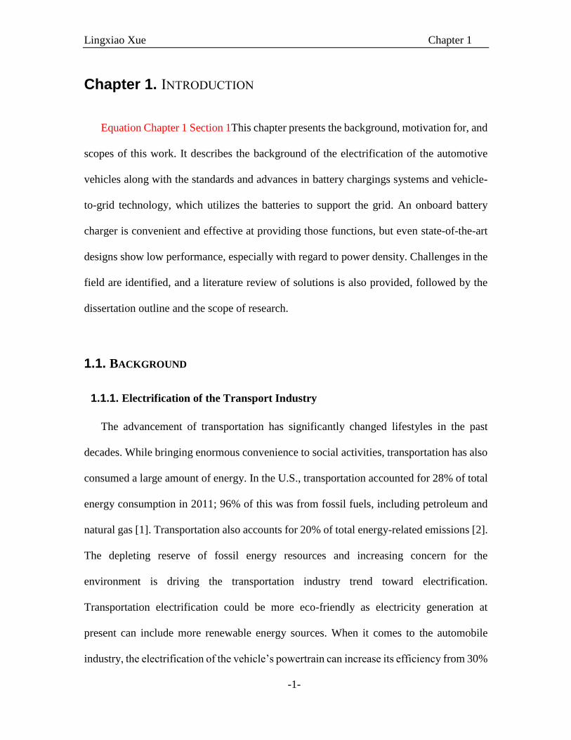
characteristic depends on the Si MOSFET, the overall device package shows a normally-
off feature, as shown in Figure 1.1.
Figure 1.1. Cascode structure combines a low voltage Si MOSFET and a depletion-mode GaN HEMT to
achieve a normally-off device
GaN devices can also be made in enhancement mode but this requires more
complicated gate structure. Four different structures for enhancement mode GaN are shown
in [43].
Most of the reported implementations of high voltage GaN devices are in cascode
structure. Transphorm, Inc., one leader in the cascode HV GaN devices arena, tested their
devices in a 760 W hard-switching boost converter with 99.2% efficiency at 100 kHz and
98.2% efficiency at 800 kHz [44]. Tranphorm also built a 1 kW, 50 kHz, 99% efficiency
totem-pole Power Factor Correction (PFC) converter [45]. Researchers at CPES, Virginia
Tech, built 1.2 kW buck converter using Transphorm devices, achieving 97.8% efficiency
at 500 kHz hard-switching and 99.1% efficiency at 500 kHz soft-switching [46]. LLC
resonant converters using same devices are also reported in [46-48] for DC/DC
applications. Implementation of Transphorm devices can also be found in switched
capacitor topologies, such as the switched capacitor three port inverter in [49], and isolated
switched capacitor DC/DC converter in [50], which claims 172 W/in3 power density.
Lingxiao Xue Chapter 1
-10-
Reference [51] also reported a Transphorm-device-based uninterruptible power supply
(UPS) with 93.8% efficiency switching at 200 kHz.
International Rectifier also announced their high voltage GaN devices in cascode
structure. They developed a 400 W, 100 kHz, 98.2% efficiency boost converter and a 200
W, 400 kHz, 93% efficiency LLC converter [52].
GaN Systems Inc. used their GaN devices, and in collaboration with APEI, built a 5
kW boost converter that showed 98.5% peak efficiency [53]. Their 600 W, 200 kHz two-
phase interleaved PFC demonstrated 97.5% efficiency [54].
Kikkawa reported a 1 MHz, 500 W PFC converter using Fujitsu cascode devices, but
the efficiency was only 86.5% [55]. Another Fujitsu GaN semi-bridge less PFC achieves
2500 W and 94.3% efficiency at 70 kHz switching frequency [56].
Very little research exists on the implementation of enhancement-mode high voltage
GaN devices. Furukawa and Sanken announced their high voltage enhancement-mode
GaN devices in 2009 [57-59] but no further power conversion application can be found.
Masahiro Ishida from Panasonic Corporation reported a 6 kHz, 1500 W, three-phase
inverter with 99.3% efficiency made using Panasonic gate injection transistors (GIT) GaN
devices [60, 61]. Another Panasonic GIT application is in PV systems. It is essentially a
2000 W boost converter that achieves a peak efficiency of 98.6% at 48 kHz [62].
To summarize, boost topology dominates the reported demonstration of high voltage
GaN devices mainly because of the simplicity of driving and feasibility of switching
waveform measurement on the hard-switching low-side device. Other emerging
applications cover the areas of motor drives, renewable energy, and computing and
consumer electronics applications. It has been widely predicted that HV GaN devices will
Lingxiao Xue Chapter 1
-11-
play important roles in the future of electric vehicle or hybrid electric vehicle power
electronics [28, 40, 43, 63-65], but so far there is hardly any research on HV GaN devices
implementation in automotive applications.
Furthermore, we can also see most literature dealing with high voltage GaN application
falls into the cascode category. The cascode structure has more intrinsic interconnection
inductance inside the device package [66]. Furthermore, the switching speed is more
difficult to control for the cascode structure [67, 68]. It is critical to figure out how to best
pair the Si and GaN devices in order to avoid the capacitance mismatch problem [69].
Therefore, enhancement-mode GaN devices are preferable. However, the research on the
implementation of enhancement-mode high voltage devices is quite limited.
1.2.3. DC Link Capacitor Reduction Technique
The Level 2 battery charger topology will be a single phase AC/DC converter since the
battery needs to be charged with a household electrical outlet. As power factor correction
(PFC) is usually required on the AC side, the AC input voltage and current will be
sinusoidal so that input power will pulsate at two times the line frequency. This pulsating
power is usually stored in capacitors that have high capacitance. Depending on the
capacitor technology, high capacitance leads to a difficult trade-off between the volume
and lifetime. For example, film capacitors have a long lifetime and low capacitance density
while electrolytic capacitors have a high capacitance but low lifetime. In automotive
applications where both volume and lifetime are critical, power density is usually sacrificed.
The size of the DC link capacitor is mainly determined by the current ripple at two times
the line frequency instead of the switching ripple [3]. The DC link capacitors therefore
Lingxiao Xue Chapter 1
-12-
become one of the battery charger’s major power density barriers, even though the
switching frequency is boosted by wide bandgap devices.
From the SiC research, we can see that the capacitor occupies 25% of the total volume
[13]. As the HRL GaN project shows, the DC link capacitor estimation will be 37.5% of
the total volume budget, even when less-reliable, high-density electrolytic capacitors are
used [70]. If film capacitors are adopted, the capacitor itself will be 1.3 times the total
volume budget, making it impossible to achieve 150W/in3 target.
The DC link capacitor is not a new issue in the single phase AC/DC converter.
Extensive research on capacitance reduction has been done for decades in applications
where long lifetime and/or high power density are required. Smaller DC link capacitance
can be reduced by allowing for higher voltage ripple [71], but the switches will suffer from
higher voltage stress. With the auxiliary circuit approach, the auxiliary energy storage can
take part of the ripple energy burden from the DC link capacitor without increasing voltage
ripple, but this solution increases the degree of complexity [72-76]. Recent research on
Lithium-Ion batteries shows that charging current with two times line frequency ripple
cause no harm to the battery at least in the short term [77-81]. Reference [79] and [80]
compares battery capacity under DC charging and pulse charging with similar current
waveform that this paper will use, and the difference is minor: 0.55% and -1.4%,
respectively. Reference [78] shows an around 2 oC temperature rise due to increased RMS
value. In all, although long-term tests on battery lifetime are certainly necessary,
preliminary results show two times line frequency ripple current causes minor impact to
battery capacity and temperature rise. Therefore, this work will adopt a charger design with
the charging current containing low-frequency ripples.

Lingxiao Xue Chapter 1
-13-
Allow the low-frequency ripples into the battery pack is not a new concept. Some single
stage converters without intermediate energy storage naturally allow low-frequency ripple
power into the batteries. However, the amount of ripple power cannot be controlled.
Furthermore, the nature of ripple power balance is not well understood especially
considering the circuit parasitics. Furthermore, there is a tradeoff between the DC link
capacitor size and the charging efficiency that needs to be quantified.
1.3. DISSERTATION MOTIVATIONS AND OBJECTIVE
This work targets at improving the power density of bidirectional PHEV battery
chargers by exploring two critical enabling technologies. One is the implementation of
GaN devices at high switching-frequency and high efficiency, which can shrink the
magnetic components and the heatsink. The other one covers the size reduction techniques
of the low frequency energy storage.
GaN devices from HRL Laboratories will be examined as they were the only available
enhancement-mode devices during the development of this work. To achieve high current
capability and reliable switching, the multi-chip module approach is adopted. Both static
and dynamic characterizations are conducted to verify the performance of the GaN module.
A boost converter is built with the module, and the converter loss is modeled. Those parts
will be covered in Chapter 2.
A topology comparison is then carried out in Chapter 3 to identify the suitable topology
candidates for the GaN bidirectional charging system. Topologies are compared with the
considerations of galvanic isolation, controllability, realization complexity, and switching
reliability. Some candidate topologies are evaluated quantitatively in terms of converter

Lingxiao Xue Chapter 1
-14-
loss and switching frequency range. This chapter ends with the selected converter topology
that will be used to build the prototypes.
Chapter 4 will address the issue of large DC link capacitors. A DC link volume
reduction technology, namely sinusoidal charging, is analyzed in great details and
implemented in a full bridge (FB) plus dual active bridge (DAB) topology. The control
strategy for the DAB stage to achieve sinusoidal charging is proposed. Loss impact on the
DC link voltage ripple is also analyzed, and closed-loop control on the DC link voltage
ripple is examined. Sinusoidal charging can significantly reduce the DC link capacitor size,
but comes with a sacrifice in charging efficiency. Different charging waveforms are then
evaluated to achieve a better tradeoff between DC link size and charging efficiency.
In the implementation of the experimental prototypes incorporating the GaN modules
and the DC link reduction techniques, several practical design challenges emerged. Those
challenges are associated with GaN devices, the DC link reduction scheme, or the
combination of the two. The challenges include the reliable driving and sensing with the
fast GaN switching, the zero-crossing current spike for GaN totem-pole PFC, and the DAB
operation modeling with the DC-link-reduction charging scheme. Chapter 5 describes and
addresses those challenges.
Chapter 6 summarizes the main contributions of this work and proposes the future work.
1.4. LIST OF REFERENCES
[1] Energy Information Administration, US Department of Energy, "Annual energy
review 2011,", 2011.
[2] S. Aso, M. Kizaki, and Y. Nonobe, "Development of Fuel Cell Hybrid Vehicles in
TOYOTA," in Power Convers. Conf., 2007, pp. 1606-1611.
Lingxiao Xue Chapter 1
-15-
[3] X. E. Yu, X. Yanbo, S. Sirouspour, and A. Emadi, "Microgrid and transportation
electrification: A review," in Proc. Transportation Electrification Conf. and Expo. ,
2012, pp. 1-6.
[4] M. Yilmaz and P. T. Krein, "Review of Battery Charger Topologies, Charging
Power Levels, and Infrastructure for Plug-In Electric and Hybrid Vehicles," IEEE
Trans. Power Electron., vol. 28, no. 5, pp. 2151-2169, 2013.
[5] C. Guille and G. Gross, "A conceptual framework for the vehicle-to-grid (V2G)
implementation," Energy Policy, vol. 37, no. 11, pp. 4379-4390, 2009.
[6] H. Lund and W. Kempton, "Integration of renewable energy into the transport and
electricity sectors through V2G," Energy policy, vol. 36, no. 9, pp. 3578-3587, 2008.
[7] B. K. Sovacool and R. F. Hirsh, "Beyond batteries: An examination of the benefits
and barriers to plug-in hybrid electric vehicles (PHEVs) and a vehicle-to-grid (V2G)
transition," Energy Policy, vol. 37, no. 3, pp. 1095-1103, 2009.
[8] M. C. Kisacikoglu, B. Ozpineci, and L. M. Tolbert, "Examination of a PHEV
bidirectional charger system for V2G reactive power compensation," in Proc. IEEE
Appl. Power Electron. Conf. Expo., 2010, pp. 458-465.
[9] I. Cvetkovic, T. Thacker, D. Dong, G. Francis, V. Podosinov, D. Boroyevich, F.
Wang, R. Burgos, G. Skutt, and J. Lesko, "Future home uninterruptible renewable
energy system with vehicle-to-grid technology," in Proc. IEEE Energy Convers.
Congr. Expo., 2009, pp. 2675-2681.
[10] W. Kempton and J. Tomić, "Vehicle-to-grid power implementation: From
stabilizing the grid to supporting large-scale renewable energy," J. of Power
Sources, vol. 144, no. 1, pp. 280-294, 2005.
[11] ARPA-E, "Financial Assistance Funding Opportunity Announcement," 2010.
[12] B. Hughes. Normally-Off GaN-on-Si Bi-Directional Automobile Battery-to -Grid
6.6kW Charger Switching at 500kHz. presented at 2014 Appl. Power Electron.
Conf. Expo. [Online]. Available: http://www.apec-conf.org/wp-
content/uploads/IS2-4-5.pdf
[13] B. Whitaker, A. Barkley, Z. Cole, B. Passmore, D. Martin, T. McNutt, et al., "A
High-Density, High-Efficiency, Isolated On-Board Vehicle Battery Charger
Utilizing Silicon Carbide Power Devices," IEEE Trans. Power Electron., vol. PP,
no. 99, pp. 1-1, 2013.
[14] C. Gyu-Yeong, K. Jong-Soo, L. Byoung-kuk, W. Chung-Yuen, and L. Tea-Won,
"A Bi-directional battery charger for electric vehicles using photovoltaic PCS
systems," in Proc. Veh. Power Propulsion Conf., 2010, pp. 1-6.
[15] M. C. Kisacikoglu, B. Ozpineci, and L. M. Tolbert, "Reactive power operation
analysis of a single-phase EV/PHEV bidirectional battery charger," in Proc. Int.
Conf. on Power Electron., 2011, pp. 585-592.
[16] Z. Xiaohu, W. Gangyao, S. Lukic, S. Bhattacharya, and A. Huang, "Multi-function
bi-directional battery charger for plug-in hybrid electric vehicle application," in
Proc. IEEE Energy Convers. Congr. Expo., 2009, pp. 3930-3936.
[17] Z. Xiaohu, S. Lukic, S. Bhattacharya, and A. Huang, "Design and control of grid-
connected converter in bi-directional battery charger for Plug-in hybrid electric
vehicle application," in Proc. Veh. Power Propulsion Conf., 2009, pp. 1716-1721.
Lingxiao Xue Chapter 1
-16-
[18] D. Gautam, F. Musavi, M. Edington, W. Eberle, and W. G. Dunford, "An
automotive on-board 3.3 kW battery charger for PHEV application," in Proc. Veh.
Power Propulsion Conf., 2011, pp. 1-6.
[19] H. J. Chae, W. Y. Kim, S. Y. Yun, Y. S. Jeong, J. Y. Lee, and H. T. Moon, "3.3kW
on board charger for electric vehicle," in Proc. Int. Conf. on Power Electron., 2011,
pp. 2717-2719.
[20] K. Jong-Soo, C. Gyu-Yeong, J. Hye-Man, L. Byoung-kuk, C. Young-Jin, and H.
Kyu-Bum, "Design and implementation of a high-efficiency on- board battery
charger for electric vehicles with frequency control strategy," in Proc. Veh. Power
Propulsion Conf., 2010, pp. 1-6.
[21] P. Junsung, K. Minjae, and C. Sewan, "Fixed frequency series loaded resonant
converter based battery charger which is insensitive to resonant component
tolerances," in Proc. Int. Power Electron. and Motion Control Conf., 2012, pp. 918-
922.
[22] L. Jun-Young and C. Hyung-Jun, "6.6-kW Onboard Charger Design Using DCM
PFC Converter With Harmonic Modulation Technique and Two-Stage DC/DC
Converter," IEEE Trans. Ind. Electron., vol. 61, no. 3, pp. 1243-1252, 2014.
[23] A. G. Cocconi, "Combined motor drive and battery recharge system," ed: Google
Patents, 1994.
[24] S. Haghbin, S. Lundmark, M. Alakula, and O. Carlson, "Grid-Connected Integrated
Battery Chargers in Vehicle Applications: Review and New Solution," IEEE Trans.
Ind. Electron., vol. 60, no. 2, pp. 459-473, 2013.
[25] T. Lixin and S. Gui-Jia, "A low-cost, digitally-controlled charger for plug-in hybrid
electric vehicles," in Proc. IEEE Energy Convers. Congr. Expo., 2009, pp. 3923-
3929.
[26] D.-G. Woo, G.-Y. Choe, J.-S. Kim, B.-K. Lee, J. Hur, and G.-B. Kang,
"Comparison of integrated battery chargers for plug-in hybrid electric vehicles:
Topology and control," in IEEE Int. Electric Mach. & Drives Conf., 2011, pp. 1294-
1299.
[27] J. W. Kolar, U. Drofenik, J. Biela, M. L. Heldwein, H. Ertl, T. Friedli, et al., "PWM
Converter Power Density Barriers," in Power Convers. Conf., 2007, pp. P-9-P-29.
[28] A. Avron, "Overview of wide band gap semiconductors in power electronics," 2013.
[29] Z. Hui, L. M. Tolbert, B. Ozpineci, and M. S. Chinthavali, "A SiC-Based Converter
as a Utility Interface for a Battery System," in Proc. Ind. Appl. Conf., 2006, pp.
346-350.
[30] S. K. Mazumder, K. Acharya, and P. Jedraszczak, "High-temperature all-SiC
bidirectional DC/DC converter for plug-in-hybrid vehicle (PHEV)," in Proc. Ann.
Conf. IEEE Ind. Electron., 2008, pp. 2873-2878.
[31] K. Acharya, S. K. Mazumder, and P. Jedraszczak, "Efficient, High-Temperature
Bidirectional Dc/Dc Converter for Plug-in-Hybrid Electric Vehicle (PHEV) using
SiC Devices," in Proc. IEEE Appl. Power Electron. Conf. Expo., 2009, pp. 642-
648.
[32] S. K. Mazumder and P. Jedraszczak, "Evaluation of a SiC dc/dc converter for plug-
in hybrid-electric-vehicle at high inlet-coolant temperature," IET Power Electron.,
vol. 4, no. 6, pp. 708-714, 2011.
Lingxiao Xue Chapter 1
-17-
[33] R. Eden, "Market Forecasts for Silicon Carbide & Gallium Nitride Power
Semiconductors," 2013.
[34] Y. Cui and L. M. Tolbert, "High step down ratio (400 V to 1 V) phase shift full
bridge DC/DC converter for data center power supplies with GaN FETs," in Proc.
IEEE Workshop on Wide Bandgap Power Devices and Appl., 2013, pp. 23-27.
[35] M. Danilovic, L. Fang, X. Lingxiao, R. Wang, P. Mattavelli, and D. Boroyevich,
"Size and weight dependence of the single stage input EMI filter on switching
frequency for low voltage bus aircraft applications," in Proc. Int. Power Electro.
and Motion Control Conf., 2012, pp. LS4a.4-1-LS4a.4-7.
[36] M. Danilovic, C. Zheng, W. Ruxi, L. Fang, D. Boroyevich, and P. Mattavelli,
"Evaluation of the switching characteristics of a gallium-nitride transistor," in Proc.
IEEE Energy Convers. Congr. Expo.,, 2011, pp. 2681-2688.
[37] F. C. Lee and L. Qiang, "High-Frequency Integrated Point-of-Load Converters:
Overview," IEEE Trans. Power Electron., vol. 28, no. 9, pp. 4127-4136, 2013.
[38] D. Reusch and F. C. Lee, "High frequency isolated bus converter with gallium
nitride transistors and integrated transformer," in Proc. IEEE Energy Convers.
Congr. Expo., 2012, pp. 3895-3902.
[39] M. Vasic, D. Diaz, O. Garcia, P. Alou, J. A. Oliver, and J. A. Cobos, "Optimal
design of envelope amplifier based on linear-assisted buck converter," in Proc.
IEEE Appl. Power Electron. Conf. Expo.,, 2012, pp. 836-843.
[40] P. Shamsi, M. McDonough, and B. Fahimi, "Performance evaluation of wide
bandgap semiconductor technologies in automotive applications," in Proc. IEEE
Workshop on Wide Bandgap Power Devices and Appl., 2013, pp. 115-118.
[41] Z. Weimin, L. Yu, Z. Zheyu, F. Wang, L. M. Tolbert, B. J. Blalock, et al.,
"Evaluation and comparison of silicon and gallium nitride power transistors in LLC
resonant converter," in Proc. IEEE Energy Convers. Congr. Expo., 2012, pp. 1362-
1366.
[42] S. Levin, "Vendor positions in the high voltage GaN commercialization race," 2013.
[43] T. Kachi, D. Kikuta, and T. Uesugi, "GaN power device and reliability for
automotive applications," in Proc. IEEE Int. Rel. Physics Symp., 2012, pp. 3D.1.1-
3D.1.4.
[44] Y. Wu, x, F, R. Coffie, N. Fichtenbaum, Y. Dora, et al., "Total GaN solution to
electrical power conversion," in Proc. Ann. Device Res. Conf., 2011, pp. 217-218.
[45] Y. F. Wu, J. Gritters, L. Shen, R. P. Smith, J. McKay, R. Barr, et al., "Performance
and robustness of first generation 600-V GaN-on-Si power transistors," in Proc.
IEEE Workshop on Wide Bandgap Power Devices and Appl., 2013, pp. 6-10.
[46] X. Huang, Z. Liu, Q. Li, and F. C. Lee, "Evaluation and application of 600V GaN
HEMT in cascode structure," IEEE Trans. Power Electron., vol. PP, no. 99, pp. 1-
1, 2013.
[47] D. Huang, S. Ji, and F. C. Lee, "Matrix transformer for LLC resonant converters,"
in Proc. IEEE Appl. Power Electron. Conf. Expo., 2013, pp. 2078-2083.
[48] Z. Weimin, X. Zhuxian, Z. Zheyu, F. Wang, L. M. Tolbert, and B. J. Blalock,
"Evaluation of 600 V cascode GaN HEMT in device characterization and all-GaN-
based LLC resonant converter," in Proc. IEEE Energy Convers. Congr. Expo.,
2013, pp. 3571-3578.
Lingxiao Xue Chapter 1
-18-
[49] C. Li, D. Jiao, M. J. Scott, C. Yao, L. Fu, X. Lu, et al., "A 2 kW Gallium Nitride
based switched capacitor three-port inverter," in Proc. IEEE Workshop on Wide
Bandgap Power Devices and Appl., 2013, pp. 119-124.
[50] X. Zhang, C. Yao, M. J. Scott, E. Davidson, J. Li, P. Xu, et al., "A GaN transistor
based 90 W isolated Quasi-Switched-Capacitor DC/DC converter for AC/DC
adapters," in Proc. IEEE Workshop on Wide Bandgap Power Devices and Appl.,
2013, pp. 15-22.
[51] R. Mitova, R. Ghosh, U. Mhaskar, D. Klikic, M.-X. Wang, and A. Dentella,
"Investigations of 600V GaN HEMT & GaN diode for the power converter
applications," IEEE Trans. Power Electron., vol. PP, no. 99, pp. 1-1, 2013.
[52] M. A. Briere, "The Status of GaN-on-Si based Power Device Development at
International Rectifier," APEC Exhibitor Presentation, March 19 2013.
[53] GaN Systems. Inc., "High efficiency 2kw-5kw boost converter," Application Brief,
2013.
[54] GaN Systems. Inc., "Power factor correction stage," Application Brief, 2013.
[55] T. Kikkawa, T. Hosoda, S. Akiyama, Y. Kotani, T. Wakabayashi, T. Ogino, et al.,
"600 V GaN HEMT on 6-inch Si substrate using Au-free Si-LSI process for power
applications," in Proc. IEEE Workshop on Wide Bandgap Power Devices and Appl.,
2013, pp. 11-14.
[56] H. Nakao, Y. Yonezawa, T. Sugawara, Y. Nakashima, T. Horie, T. Kikkawa, et al.,
"2.5-kW power supply unit with semi-bridgeless PFC designed for GaN-HEMT,"
in Proc. IEEE Appl. Power Electron. Conf. Expo., 2013, pp. 3232-3235.
[57] H. Kambayashi, Y. Satoh, Y. Niiyama, T. Kokawa, M. Iwami, T. Nomura, et al.,
"Enhancement-mode GaN hybrid MOS-HFETs on Si substrates with Over 70 A
operation," in Proc. Int. Symp. Power Semiconductor Devcies & IC's, 2009, pp. 21-
24.
[58] N. Kaneko, O. Machida, M. Yanagihara, S. Iwakami, R. Baba, H. Goto, et al.,
"Normally-off AlGaN/GaN HFETs using NiOx gate with recess," in Proc. Int.
Symp. Power Semiconductor Devcies & IC's, 2009, pp. 25-28.
[59] Y. Niiyama, S. Ootomo, H. Kambayashi, N. Ikeda, T. Nomura, and S. Kato,
"Normally-Off Operation GaN Based MOSFETs for Power Electronics," in Proc.
Ann. IEEE Compound Semiconductor Integrated Circuit Symp., 2009, pp. 1-4.
[60] M. Ishida, T. Ueda, T. Tanaka, and D. Ueda, "GaN on Si Technologies for Power
Switching Devices," IEEE Trans. Electron. Devices, vol. 60, no. 10, pp. 3053-3059,
2013.
[61] D. Ueda, "Status Quo and trends of GaN power devices," in Proc. IEEE Int. Rel.
Physics Symp., 2013, pp. 3C.2.1-3C.2.4.
[62] A. Hensel, C. Wilhelm, and D. Kranzer, "Application of a new 600 V GaN
transistor in power electronics for PV systems," in Proc. Int. Power Electro. and
Motion Control Conf., 2012, pp. DS3d.4-1-DS3d.4-5.
[63] K. S. Boutros, C. Rongming, and B. Hughes, "GaN power electronics for
automotive application," in Proc. IEEE Energytech, 2012, pp. 1-4.
[64] E. Sönmez, "Efficient high-voltage GaN devices and ICs for next generation power
management solutions."
Lingxiao Xue Chapter 1
-19-
[65] Y. Wu, J. Gritters, L. Shen, R. Smith, and B. Swenson, "kV-class GaN-on-Si
HEMTs Enabling 99% Efficiency Converter at 800 V & 100 kHz," IEEE
Trans. Power Electron., vol. PP, no. 99, pp. 1-1, 2013.
[66] L. Zhengyang, H. Xiucheng, F. C. Lee, and L. Qiang, "Package Parasitic
Inductance Extraction and Simulation Model Development for the High-Voltage
Cascode GaN HEMT," IEEE Trans. Power Electron., vol. 29, no. 4, pp. 1977-1985,
2014.
[67] D. Aggeler, J. Biela, and J. W. Kolar, "Controllable du/dt behaviour of the SiC
MOSFET/JFET cascode an alternative hard commutated switch for telecom
applications," in Proc. IEEE Appl. Power Electron. Conf. Expo., 2010, pp. 1584-
1590.
[68] W. Saito, Y. Saito, H. Fujimoto, A. Yoshioka, T. Ohno, T. Naka, et al., "Switching
controllability of high voltage GaN-HEMTs and the cascode connection," in Proc.
Int. Symp. Power Semiconductor Devcies & IC's, 2012, pp. 229-232.
[69] X. Huang, Z. Liu, F. C. Lee, and Q. Li, "Characterization and Enhancement of
High-Voltage Cascode GaN Devices," IEEE Trans. Electron. Devices, vol. PP, no.
99, pp. 1-1, 2014.
[70] X. Lingxiao, D. Diaz, S. Zhiyu, L. Fang, P. Mattavelli, and D. Boroyevich, "Dual
active bridge based battery charger for plug-in hybrid electric vehicle with charging
current containing low frequency ripple," in Proc. IEEE Appl. Power Electron.
Conf. Expo., 2013, pp. 1920-1925.
[71] D. Dong, D. Boroyevich, W. Ruxi, and I. Cvetkovic, "A two-stage high power
density single-phase ac-dc bi-directional PWM converter for renewable energy
systems," in Proc. IEEE Energy Convers. Congr. Expo., 2010, pp. 3862-3869.
[72] T. Shimizu, T. Fujita, G. Kimura, and J. Hirose, "A unity power factor PWM
rectifier with DC ripple compensation," IEEE Trans. Ind. Electron., vol. 44, no. 4,
pp. 447-455, 1997.
[73] T. Shimizu, Y. Jin, and G. Kimura, "DC ripple current reduction on a single-phase
PWM voltage-source rectifier," IEEE Trans. Ind. Appl., vol. 36, no. 5, pp. 1419-
1429, 2000.
[74] Y. X. Qin, H. S. H. Chung, D. Y. Lin, and S. Y. R. Hui, "Current source ballast for
high power lighting emitting diodes without electrolytic capacitor," in Proc. Ann.
Conf. IEEE Ind. Electron. 2008, pp. 1968-1973.
[75] W. Ruxi, F. Wang, L. Rixin, N. Puqi, R. Burgos, and D. Boroyevich, "Study of
Energy Storage Capacitor Reduction for Single Phase PWM Rectifier," in Proc.
IEEE Appl. Power Electron. Conf. Expo., 2009, pp. 1177-1183.
[76] A. K. Verma, B. Singh, and D. T. Shahani, "Vehicle to grid and grid to vehicle
bidirectional power flow at unity power factor with DC ripple compensation," in
Proc. IEEE Int. Conf. Ind. and Inform. Syst., 2012, pp. 1-6.
[77] M. Uno and K. Tanaka, "Influence of High-Frequency Charge/Discharge Cycling
Induced by Cell Voltage Equalizers on the Life Performance of Lithium-Ion Cells,"
IEEE Trans. Veh. Technol., vol. 60, no. 4, pp. 1505-1515, 2011.
[78] S. Bala, T. Tengner, P. Rosenfeld, and F. Delince, "The effect of low frequency
current ripple on the performance of a Lithium Iron Phosphate (LFP) battery energy
storage system," in Proc. IEEE Energy Convers. Congr. Expo., 2012, pp. 3485-
3492.

Lingxiao Xue Chapter 1
-20-
[79] K. Tae-Hoon, J. Jin-Beom, L. Baek-Haeng, S. Dong-Hyun, S. Hyun-Sik, K.
Byoung-Hoon, et al., "Analytical study on low-frequency ripple effect of battery
charging," in Proc. IEEE Veh. Power Propulsion Conf.,, 2012, pp. 809-811.
[80] H. Z. Beh, G. A. Covic, and J. T. Boys, "Effects of pulse and DC charging on
lithium iron phosphate (LiFePO4) batteries," in Proc. IEEE Energy Convers. Congr.
Expo., 2013, pp. 315-320.
[81] L.-R. Chen, S.-L. Wu, D.-T. Shieh, and T.-R. Chen, "Sinusoidal ripple current
charging strategy and optimal charging frequency for Li-ion batteries," IEEE Trans.
Ind. Electron., vol. 60, no. 1, pp. 88-97, 1997.
Lingxiao Xue Chapter 2
-21-
Chapter 2. HRL GAN DEVICES AND MULTI-CHIP MODULE
CHARACTERIZATION
Equation Chapter (Next) Section 1Power semiconductors are one of the main
fundamental elements of the system. As the main driving force for high switching
frequency, the characteristics of those switches need to be understood correctly. In this
chapter, the HRL GaN technology will be briefly reviewed and the multi-chip module will
be characterized. This characterization will facilitate the analysis and design in the
following chapters.
2.1. HRL GAN TRANSISTOR TECHNOLOGY
In 2011, Rongming Chu of HRL Laboratories, LLC, reported a 1200V normally off
GaN-on-Si transistor [1]. In order to realize normally-off, a halide-based plasma treatment
plus insulated gate solution was used. The F- and Cl- based plasma treatment was
performed in the gate region to shift the threshold voltage from negative to positive. The
gate insulator was formed by Al2O3 to achieve low gate-leakage current. The device has
one gate and two source field plates. The field plates reduce the electric field in the gate-
drain region, which benefits the breakdown voltage and dynamic on-resistance. The
threshold voltage of this device is around 0.6V. The maximum positive voltage is 3 V.
Packaged in a low inductance SMD, the GaN transistor can switch 350V and 20A in 15 ns
[2]. This generation of devices is designated as GEN 3.
In a later design, no F-plasma treatment was used, and an AlN-based dielectric instead
of Al2O3 was used as the gate insulator. This new design brought the threshold voltage to

Lingxiao Xue Chapter 2
-22-
1.3 V, reduced the on-resistance, and increased both the maximum drain current and the
maximum positive gate bias voltage [3, 4]. With ultra-low resistance and inductance gate
drive, this generation of devices switched 400 V within 1.4 ns, achieving an unprecedented
high dv/dt of 325 V/ns. The corresponding boost converter switching at 200 kHz, 400 V
and 50% duty cycle demonstrated 98% efficiency at 1.7 kW power [5]. This generation of
devices is designated as GEN 4.
Those two generations of devices—GEN 3 and GEN 4—will be used in this work to
build the battery chargers.
2.2. CONCEPT OF GAN MULTI-CHIP MODULE
From the characterization results in the previous section, we know that the maximum
current of the HRL discrete device is below 10 A at the suggested driving voltage. Usually,
the rated device current is much lower than this maximum current due to thermal
considerations. In fact, the GEN 3 device is rated at 3 A, and the GEN 4 device is rated at
5A. The current rating of a single GaN device is too low for the battery charger of the plug-
in hybrid electric vehicle, which requires kW power in this work. Therefore, devices must
be paralleled to achieve the high current capability. The device paralleling can be either
realized at SMD package level or at die level.
The SMD package of the HRL discrete device in has lower leads inductance than that
of traditional through-hole TO-220 or TO-247 packages. However, inductances created by
the internal wire bonds are inevitable. A finite element analysis by Ansoft Q3D shows that
the drain connection creates 1.7 nH inductance, and the gate connection creates 5.5 nH
inductance. Those inductances do not cause severe problems for traditional silicon devices
because of relatively large parasitic capacitance and the low current slew rate at switching
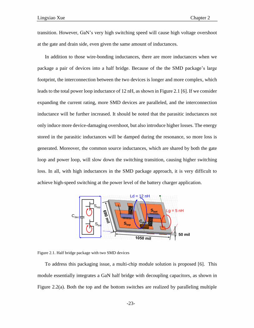
Lingxiao Xue Chapter 2
-23-
transition. However, GaN’s very high switching speed will cause high voltage overshoot
at the gate and drain side, even given the same amount of inductances.
In addition to those wire-bonding inductances, there are more inductances when we
package a pair of devices into a half bridge. Because of the the SMD package’s large
footprint, the interconnection between the two devices is longer and more complex, which
leads to the total power loop inductance of 12 nH, as shown in Figure 2.1 [6]. If we consider
expanding the current rating, more SMD devices are paralleled, and the interconnection
inductance will be further increased. It should be noted that the parasitic inductances not
only induce more device-damaging overshoot, but also introduce higher losses. The energy
stored in the parasitic inductances will be damped during the resonance, so more loss is
generated. Moreover, the common source inductances, which are shared by both the gate
loop and power loop, will slow down the switching transition, causing higher switching
loss. In all, with high inductances in the SMD package approach, it is very difficult to
achieve high-speed switching at the power level of the battery charger application.
Figure 2.1. Half bridge package with two SMD devices
To address this packaging issue, a multi-chip module solution is proposed [6]. This
module essentially integrates a GaN half bridge with decoupling capacitors, as shown in
Figure 2.2(a). Both the top and the bottom switches are realized by paralleling multiple
Ld = 12 nH
Lg = 5 nH
Stop
Sbot
Cdec
Cdec
Sbot
Stop
50 mil
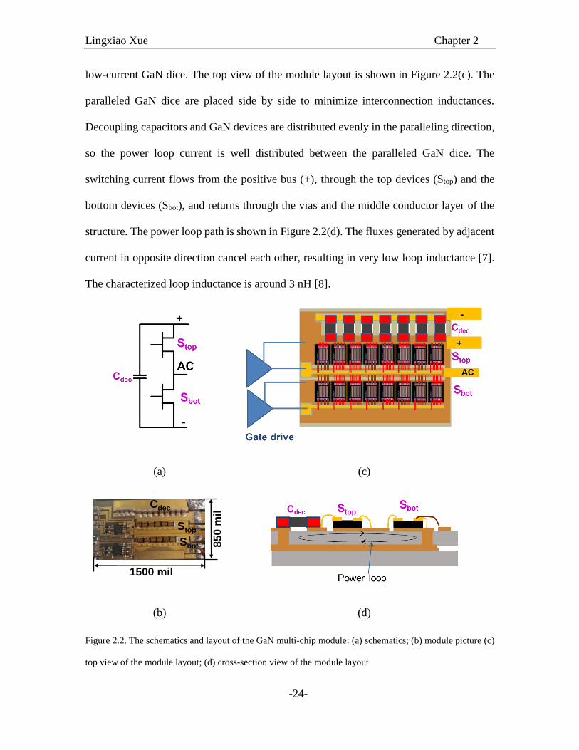
Lingxiao Xue Chapter 2
-24-
low-current GaN dice. The top view of the module layout is shown in Figure 2.2(c). The
paralleled GaN dice are placed side by side to minimize interconnection inductances.
Decoupling capacitors and GaN devices are distributed evenly in the paralleling direction,
so the power loop current is well distributed between the paralleled GaN dice. The
switching current flows from the positive bus (+), through the top devices (Stop) and the
bottom devices (Sbot), and returns through the vias and the middle conductor layer of the
structure. The power loop path is shown in Figure 2.2(d). The fluxes generated by adjacent
current in opposite direction cancel each other, resulting in very low loop inductance [7].
The characterized loop inductance is around 3 nH [8].
(a) (c)
(b) (d)
Figure 2.2. The schematics and layout of the GaN multi-chip module: (a) schematics; (b) module picture (c)
top view of the module layout; (d) cross-section view of the module layout
Stop
Sbot
Cdec
1500 mil
850
mil
Lingxiao Xue Chapter 2
-25-
The paralleled GaN switches are connected to the gate driver by a 0.5 mil thick flexible
PCB, which acts as a vertical loop to reduce the gate inductance [8]. Therefore, even though
the gate driver feeds the GaN switches from the side of the module, the mismatch of gate-
current distribution is minimized. The gate driver is implemented by two 50 mΩ Si bare
MOSFETs to minimize both inductance and resistance in the gate loop. This design reduces
the ringing and increases the switching speed, so the switching loss can be further reduced.
Without external gate resistance, the module can switch 400 V with 1.4 ns, and also
demonstrate an instantaneous switching speed of 325 V/ns [4, 8].
The module also shows superior thermal performance. The GaN switches are soldered
on a thin, high thermal conductivity, silicon nitride substrate, which is further soldered to
a micro-impingement cooler [8]. The characterized thermal resistance is 0.6 oC/W to the
coolant.
2.3. CHARACTERIZATION OF GAN MCM
This section will focus on the characterization of the GaN multi-chip module. Because
decoupling capacitors are integrated within the module, the characterization approach with
a curve tracer becomes inaccurate. To avoid generating heat to the device under test (DUT),
the curve tracer only supplies pulsed energy with very low duty cycle. The pulse current
will not only flow through the DUT, but also an alternative path completed by the
complementary switch and the decoupling capacitors. Therefore, the current measurement
is inaccurate, meaning that the characterization results would be questionable.
The influence of the alternative path can be minimized by removing either the
decoupling capacitors or the complementary switches. However, as it is very difficult to

Lingxiao Xue Chapter 2
-26-
solder them back reliably after the tests. This method is considered destructive and is
therefore rejected.
In this section, we will use a non-destructive method to characterize the conduction and
switching performance of this GaN MCM. The results will used in the topology selection
and system design in later chapters.
2.3.1. Conduction Performance Characterization
The schematics for measuring the on-state conduction characteristics are shown in
Figure 2.3. Figure 2.3 (a) and Figure 2.3 (b) describe the measurement setup in the forward
and reverse conduction conditions, respectively. In the case of forward conduction, the
switch is operating in the first quadrant, so a positive voltage Vgp is applied at the gate,
turning on the switch. The complementary switch, not drawn in the schematics, is kept off
by controlling the gate voltage to be lower than the threshold value. To avoid the current
distribution to the alternative path, a DC current source is used instead of a pulsed current
source to excite the switch. Both the excitation current and the voltage drop are measured
by precision multimeters. The on-resistance is then calculated by implementing Ohm’s law.
Particular attention needs to be paid to completing the measurement quickly without
generating any apparent temperature rise in the device. In practice, we completed the
measurement within 10 seconds with a liquid flow. The temperature rise was negligible.
A similar concept can be used for the reverse conduction measurement. The only
difference is that the switch gate is biased at the off-state negative voltage Vgn. The current
direction is changed to flow through the switch in the reverse direction.

Lingxiao Xue Chapter 2
-27-
G
D
SVgp
Vds
Ids
+
-
G
D
SIsd
+
-
Vsd
Vgd
Vgn
(a) (b)
Figure 2.3. Measurement circuit for on-state conduction characteristics: (a) on-resistance with forward
current; (b) voltage drop with reverse current
The on-resistance measurement results of a GEN 3 MCM are shown in Figure 2.4. Tis
MCM has six GEN 3 devices in parallel for both the high side and the low side switches.
The driving voltages of the GEN 3 MCM at on and off states are +2.5 V and -1.3 V,
respectively. The device’s junction temperature is measured as 32 oC; the heat is generated
by the gate driver chip inside the MCM. The on-resistance of forward direction at different
junction temperatures is plotted in Figure 2.5. The voltage drop at different currents is
shown in Figure 2.6. At low current, the voltage drop is dominated by the joint effect of
the negative drive voltage (-1.3V) and the threshold voltage (0.65V). At high current, the
gate-to-drain voltage Vgd increases to accommodate the increased current, so the voltage
drop Vsd will also increase according to (2.1).
gssd gdV V V (2.1)
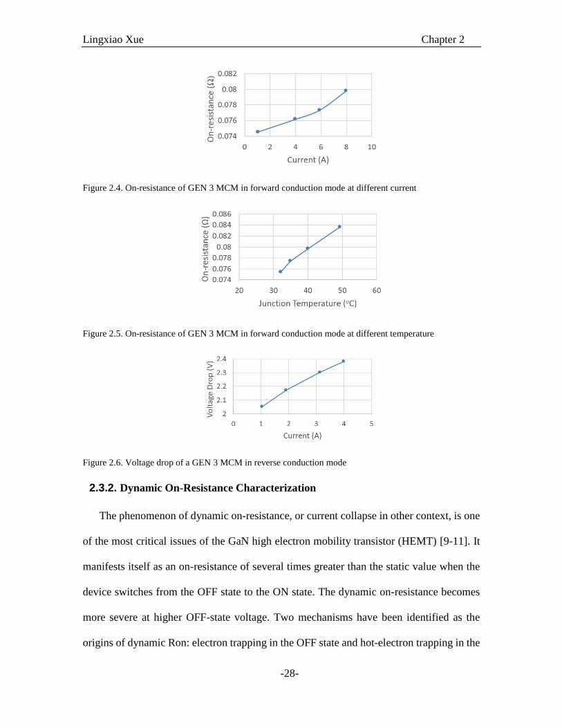
Lingxiao Xue Chapter 2
-28-
Figure 2.4. On-resistance of GEN 3 MCM in forward conduction mode at different current
Figure 2.5. On-resistance of GEN 3 MCM in forward conduction mode at different temperature
Figure 2.6. Voltage drop of a GEN 3 MCM in reverse conduction mode
2.3.2. Dynamic On-Resistance Characterization
The phenomenon of dynamic on-resistance, or current collapse in other context, is one
of the most critical issues of the GaN high electron mobility transistor (HEMT) [9-11]. It
manifests itself as an on-resistance of several times greater than the static value when the
device switches from the OFF state to the ON state. The dynamic on-resistance becomes
more severe at higher OFF-state voltage. Two mechanisms have been identified as the
origins of dynamic Ron: electron trapping in the OFF state and hot-electron trapping in the
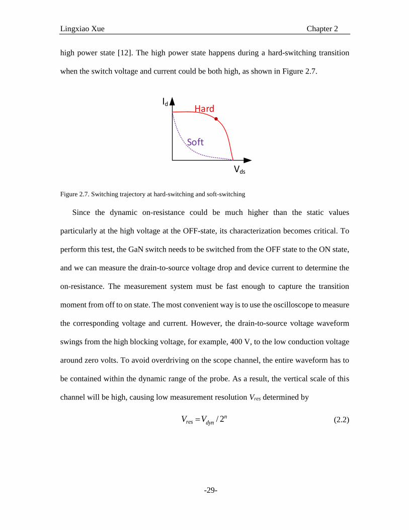
Lingxiao Xue Chapter 2
-29-
high power state [12]. The high power state happens during a hard-switching transition
when the switch voltage and current could be both high, as shown in Figure 2.7.
Vds
Soft
HardId
Figure 2.7. Switching trajectory at hard-switching and soft-switching
Since the dynamic on-resistance could be much higher than the static values
particularly at the high voltage at the OFF-state, its characterization becomes critical. To
perform this test, the GaN switch needs to be switched from the OFF state to the ON state,
and we can measure the drain-to-source voltage drop and device current to determine the
on-resistance. The measurement system must be fast enough to capture the transition
moment from off to on state. The most convenient way is to use the oscilloscope to measure
the corresponding voltage and current. However, the drain-to-source voltage waveform
swings from the high blocking voltage, for example, 400 V, to the low conduction voltage
around zero volts. To avoid overdriving on the scope channel, the entire waveform has to
be contained within the dynamic range of the probe. As a result, the vertical scale of this
channel will be high, causing low measurement resolution Vres determined by
/ 2nres dyn
V V (2.2)

Lingxiao Xue Chapter 2
-30-
where n is the bit of the analog-to-digital converter of the scope, and Vdyn is the dynamic
range of the oscilloscope channel. It is preferable to measure a waveform with low vertical
range.
A clamp circuit is used to achieve fast and accurate dynamic on-resistance
measurement [13]. Figure 2.8 illustrates the measurement setup for the on-resistance of the
bottom switch in the half-bridge.
Vdc
Vaux
Vclamp
Vds
Clamp circuit
Rclamp
Rg
Q
D
DUT
Iclamp
Figure 2.8. Clamp circuit for dynamic on-resistance measurement
The clamp circuit consists of a high voltage, low current silicon MOSFET Q, a low
voltage, fast diode, and two resistors Rg and Rclamp. An external DC voltage Vaux is needed
to drive the clamping MOSFET, and its value has to be high enough to fully turn on the
MOSFET. The operating principle of the clamping circuit is explained as follows.
When the device under test (DUT) is in the conduction mode, the drain-to-source
voltage Vds,DUT is low. Since Vaux keeps the MOSFET on, Vds,DUT is divided by the
MOSFET channel resistor Rds(on),Q and the clamping resistor Rclamp:
( ),
( ),
, clamp ds on Q
clamp
clamp ds dsclamp ds on Q
if R RR
V V VR R
(2.3)
We can see the clamping resistor needs to be high enough for accurate measurement.

Lingxiao Xue Chapter 2
-31-
When the DUT is in the blocking mode, the drain-to-source voltage Vds,DUT becomes
the bus voltage Vdc. If the clamping MOSFET is still on, the clamping resistor will have
large voltage drop, reducing the gate voltage of the clamping MOSFET, because of
, auxgs Q clampV V V (2.4).
In the blocking state, the clamping circuit should satisfy
, auxgs Q clamp clampV V I R (2.5)
, ,,( )th Q fs Qgs QclampV gI V (2.6)
where Vth,Q and gfs,Q are the threshold voltage and the transfer conductance of the clamping
MOSFET, respectively. Since the clamped voltage should always be lower than the
auxiliary power supply voltage, and the clamping resistance is in the range of kilo ohms
(the reason will be given later), the channel current Iclamp is very small. Therefore, the
steady state voltage of the clamping MOSFET is almost equal to its threshold voltage, so
it further yields
,aux th QclampVV V (2.7)
To achieve low clamping voltage in the block state, it is preferred to select a MOSFET
which requires a low Vaux to fully turn on the switch and a high Vth,Q. As a result, the
clamping circuit output maintains the information of the low DUT voltage in the
conduction mode according to (2.3) and converts the high DUT voltage in blocking mode
into a low voltage(2.7). The clamp circuit voltage has much narrower dynamic range than
the original DUT voltage such that more accurate measurement can be accomplished by an
oscilloscope.

Lingxiao Xue Chapter 2
-32-
Figure 2.9 shows the waveforms of the clamping circuit measuring the drain-to-source
voltage of the bottom switch in a double pulse test. We can see the 250 V OFF-state voltage
is clamped to around 4 - 6 V, leading to much higher resolution of the voltage measurement
at the ON state.
Figure 2.9. Double pulse test of a GEN 4 MCM at 250V/9A
Special attention must be paid to the dynamic performance of the clamp circuit when
selecting the component values. We can see that from the OFF to ON state, the Vclamp has
a slow slope transient before it reaches the designated clamp voltage. This slope is due to
the charging process of the Cgs and Cds of the MOSFET through the clamp resistor Rclamp.
Therefore, to reduce the time constant, a MOSFET with small parasitic capacitances and a
small Rclamp are preferred. The reduction of Rclamp is limited by the measurement accuracy
of the on-time voltage drop, which requires a high Rclamp value. A design tradeoff results a
value around several kilo ohms.
Meanwhile, at both the turn-on and turn-off transitions of the Si MOSFET, the parasitic
capacitors of the Si MOSFET will resonate with the parasitic inductance in the
measurement loop. In particular, the resonance at the transitions between the ON-state and
OFF-state must be skipped until the waveforms stabilize to make a trustworthy voltage
Vds (100 V/div)
Vclamp (0.9 V/div)
400 ns/divOFF ON
Lingxiao Xue Chapter 2
-33-
drop measurement. Therefore, the measurement loop inductance needs to be minimized.
The gate resistor Rg can effectively damp the resonance. However, too big Rg
compromises the clamping effect because (2.4) is not valid anymore. The selection of Rg
therefore requires a tradeoff between damping effect and clamping effect. A good
compromise leads to a value of several ohms.
Furthermore, the clamp diode D is used to prevent the gate-to-source voltage of the
clamping MOSFET from being too negative during the transient, so the measured clamped
voltage can be kept low and not exceed Vaux.
With the clamping circuit, the dynamic on-resistance of a GEN 4 GaN MCM which
has five GaN devices in parallel is characterized. The device under test (DUT) has five
GEN 4 GaN devices in parallel. Three tests of dynamic on-resistance measurement were
conducted on the low side switch of the MCM.
Test 1: double pulse test (DPT). The dynamic on-resistance measurement was recorded
after the device under test (DUT) was turned on at the designed voltage and current. The
blocking voltage was swept from 10 V to 250 V. The device current was kept around 3.5
A.
Test 2: Boost converter test. The low side switch (DUT) is in the hard-switching (HS)
condition. The switching voltage was swept from 10 V to 250 V while the switching current
was kept around 2 A. This means the input current of the Boost converter is around 2 A.
Test 3: Buck converter test. The low side switch (DUT) is in zero-voltage switching
(ZVS) condition. The switching voltage was swept from 10 V to 250 V while the switching
current was kept around 2 A, meaning that the output current of the buck converter is
around 2 A.
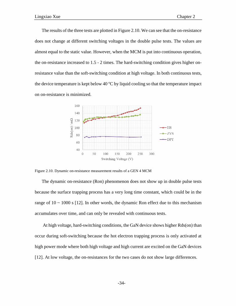
Lingxiao Xue Chapter 2
-34-
The results of the three tests are plotted in Figure 2.10. We can see that the on-resistance
does not change at different switching voltages in the double pulse tests. The values are
almost equal to the static value. However, when the MCM is put into continuous operation,
the on-resistance increased to 1.5 - 2 times. The hard-switching condition gives higher on-
resistance value than the soft-switching condition at high voltage. In both continuous tests,
the device temperature is kept below 40 oC by liquid cooling so that the temperature impact
on on-resistance is minimized.
Figure 2.10. Dynamic on-resistance measurement results of a GEN 4 MCM
The dynamic on-resistance (Ron) phenomenon does not show up in double pulse tests
because the surface trapping process has a very long time constant, which could be in the
range of 10 ~ 1000 s [12]. In other words, the dynamic Ron effect due to this mechanism
accumulates over time, and can only be revealed with continuous tests.
At high voltage, hard-switching conditions, the GaN device shows higher Rds(on) than
occur during soft-switching because the hot electron trapping process is only activated at
high power mode where both high voltage and high current are excited on the GaN devices
[12]. At low voltage, the on-resistances for the two cases do not show large differences.
Lingxiao Xue Chapter 2
-35-
The dynamic on-resistance needs to be considered in order to model converter loss and
predict converter performance. Using only the static values will lead to underestimated
conduction loss.
2.3.3. Output Charge and Capacitance Characterization
The parasitic capacitances of a GaN switch determine the switching speed and the
switching losses. For a high voltage device (over 600V), the output capacitance and the
corresponding charge are critical. In a converter with zero-voltage switching (ZVS)
capability, the capacitances not only determine the energy and timing required to achieve
ZVS but also can predict the switching losses at conditions of ZVS, partial-ZVS, or hard-
switching. However, the manufacturer datasheet usually only provides the nonlinear
capacitance curves with respect to the bias voltage. It leaves the end users to integrate the
curves to determine the charge and energy values. For the multi-chip module approach that
we are using, the package itself may introduce parasitic capacitances. Therefore, it is
necessary to characterize the charge and capacitance values for the module.
Because of the decoupling capacitors in the module, the traditional method of using a
curve tracer becomes inapplicable. We have employed two methods to measure the charge
and capacitance of the module with integrated decoupling capacitors.
The first method uses the half-bridge open-circuit measurement, as shown in Figure
2.11. Biased by a DC source, the two devices in the half-bridge module switch
complementarily with 50% duty cycle at the switching frequency of fs. In each switching
period, both switches are turned on and off once. Therefore, the charge provided by the DC
voltage source equals to the total charge of the two switches, which are biased at the voltage
of the DC source. The module decoupling capacitors and additional external capacitors in
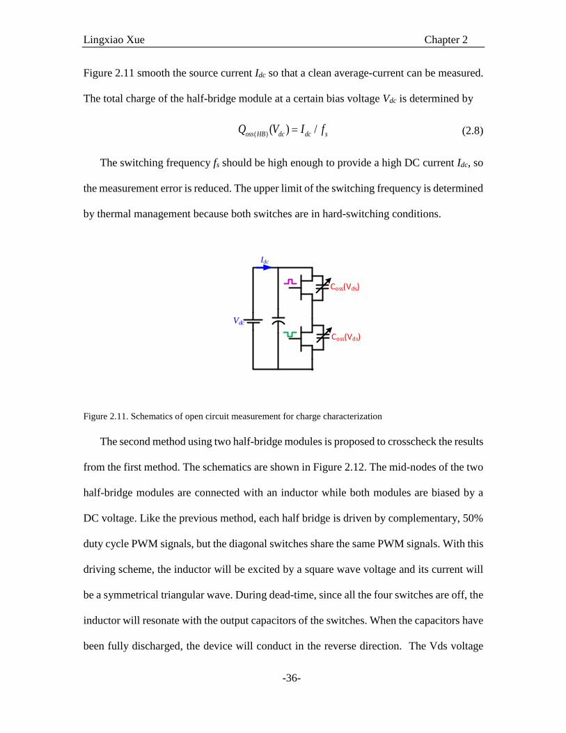
Lingxiao Xue Chapter 2
-36-
Figure 2.11 smooth the source current Idc so that a clean average-current can be measured.
The total charge of the half-bridge module at a certain bias voltage Vdc is determined by
( ) ( ) /oss HB dc dc sQ V I f (2.8)
The switching frequency fs should be high enough to provide a high DC current Idc, so
the measurement error is reduced. The upper limit of the switching frequency is determined
by thermal management because both switches are in hard-switching conditions.
Idc
Coss(Vds)
Coss(Vds)
Vdc
Figure 2.11. Schematics of open circuit measurement for charge characterization
The second method using two half-bridge modules is proposed to crosscheck the results
from the first method. The schematics are shown in Figure 2.12. The mid-nodes of the two
half-bridge modules are connected with an inductor while both modules are biased by a
DC voltage. Like the previous method, each half bridge is driven by complementary, 50%
duty cycle PWM signals, but the diagonal switches share the same PWM signals. With this
driving scheme, the inductor will be excited by a square wave voltage and its current will
be a symmetrical triangular wave. During dead-time, since all the four switches are off, the
inductor will resonate with the output capacitors of the switches. When the capacitors have
been fully discharged, the device will conduct in the reverse direction. The Vds voltage

Lingxiao Xue Chapter 2
-37-
transition waveform is also shown in Figure 2.12. The total charge for the half bridge can
be derived as
( )0
( )dt
oss HB dc L L dQ V i dt I t (2.9)
given that inductor current is almost constant during the transition. The switching
frequency and inductance should be selected to ensure relatively high inductor current and
transition time for the sake of measurement accuracy.
Coss(Vds)
Coss(Vds)
Vdc
Coss(Vds)
Coss(Vds)
iL
vds+
-
td
IL
Vds
Figure 2.12. Schematics of full bridge ZVS measurement for charge characterization
The charge measurement results of the GEN 3 and GEN 4 modules acquired by the two
methods are shown in Figure 2.13. Both GEN 3 and GEN 4 modules have six devices in
parallel to build the top or bottom switch. We can see that the charge curves do not increase
linearly with respect to the bias voltage, which can be explained by the nonlinearity of the
device capacitances. Both measurement methods, the open circuit (OC) and the full bridge
ZVS (FB_ZVS) show similar measurement results. It is also noticeable that GEN 4 MCM
has higher overall charge than the GEN 3 MCM.
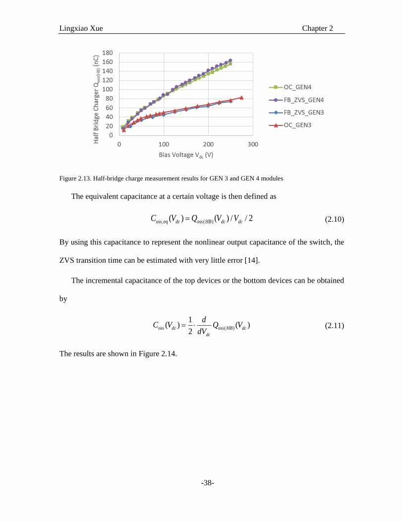
Lingxiao Xue Chapter 2
-38-
Figure 2.13. Half-bridge charge measurement results for GEN 3 and GEN 4 modules
The equivalent capacitance at a certain voltage is then defined as
,eq ( )( ) ( ) / / 2oss dc oss HB dc dcC V Q V V (2.10)
By using this capacitance to represent the nonlinear output capacitance of the switch, the
ZVS transition time can be estimated with very little error [14].
The incremental capacitance of the top devices or the bottom devices can be obtained
by
( )
1( ) ( )
2oss dc oss HB dc
dc
dC V Q V
dV (2.11)
The results are shown in Figure 2.14.

Lingxiao Xue Chapter 2
-39-
Figure 2.14. Incremental (or small signal) output capacitance of the half bridge MCM.
The energy stored in the output capacitance of the MCM for one half-bridge Eoss(HB) is
determined by
( ) ( )( )oss HB dc dc oss HBE V V dQ (2.12).
The stored energy of the half bridge is plotted against the bias voltage in Figure 2.15. Note
that the stored energy for one single device, either the top or bottom device, will be one-
half of the measured value.
Figure 2.15. Eoss of the GEN 4 GaN MCM
0
0.2
0.4
0.6
0.8
1
1.2
0 50 100 150 200 250 300
Incre
men
tal C
ap
acita
nce C
oss
(nF
)
Bias Voltage (V)
0
2
4
6
8
10
12
14
16
18
0 50 100 150 200 250 300
Eo
ss (
µJ)
Bias Voltage (V)

Lingxiao Xue Chapter 2
-40-
The performance of the GaN MCM (5 devices in parallel) is compared with other GaN
devices and state-of-the-art silicon MOSFETs, in terms of on-resistance, output charge,
output capacitance, and reverse recovery charge. Devices with very similar on-resistance
are chosen for a more fair comparison. For the HRL GaN MCM, the dynamic on-resistance
at 250 V is used. Si super junction MOSFETs from Infineon are selected. The Infineon C7
family devices are most suitable for Boost PFC applications while the CFD family devices
are designed for soft-switching converters. GEN 3 MCM (6 devices in parallel to match
the on-resistance of GEN 4) and a cascode GaN device from Transhporm are also compared.
Since the dynamic on-resistance of TPS2006PS has not been characterized, the static
resistance value is used. After this process, all the characteristics are normalized towards
HRL GEN 4 MCM, so they can be compared in one chart, as shown in Figure 2.16. The
chart also shows the reverse recovery charge for different devices. It is worth mentioning
that the GaN transistor is a majority-carrier device such that there is no reverse recovery
charge for the minority carrier. The only required charge to build up its blocking voltage
is the device output-charge. Therefore for GaN devices, the Qrr value can be approximated
by its Qoss value at the bias voltage. The Qrr values of different devices have been scaled
to 250 V, 20 A, and 100 A/µs.
As shown in Figure 2.16, the GEN 3 MCM has almost half the charge of the GEN 4
MCM, given the same on-resistances. The Transphorm TPH3006PS transistor has charge
numbers between that of GEN 4 and GEN 3 MCMs. All the GaN devices exhibit much
lower reverse recovery charge than the Si devices, which means the GaN switches
outperforms the Si counterparts in the applications where fast body diodes are required.
Also, GaN devices also show lower output charge, which reduces the transition time in
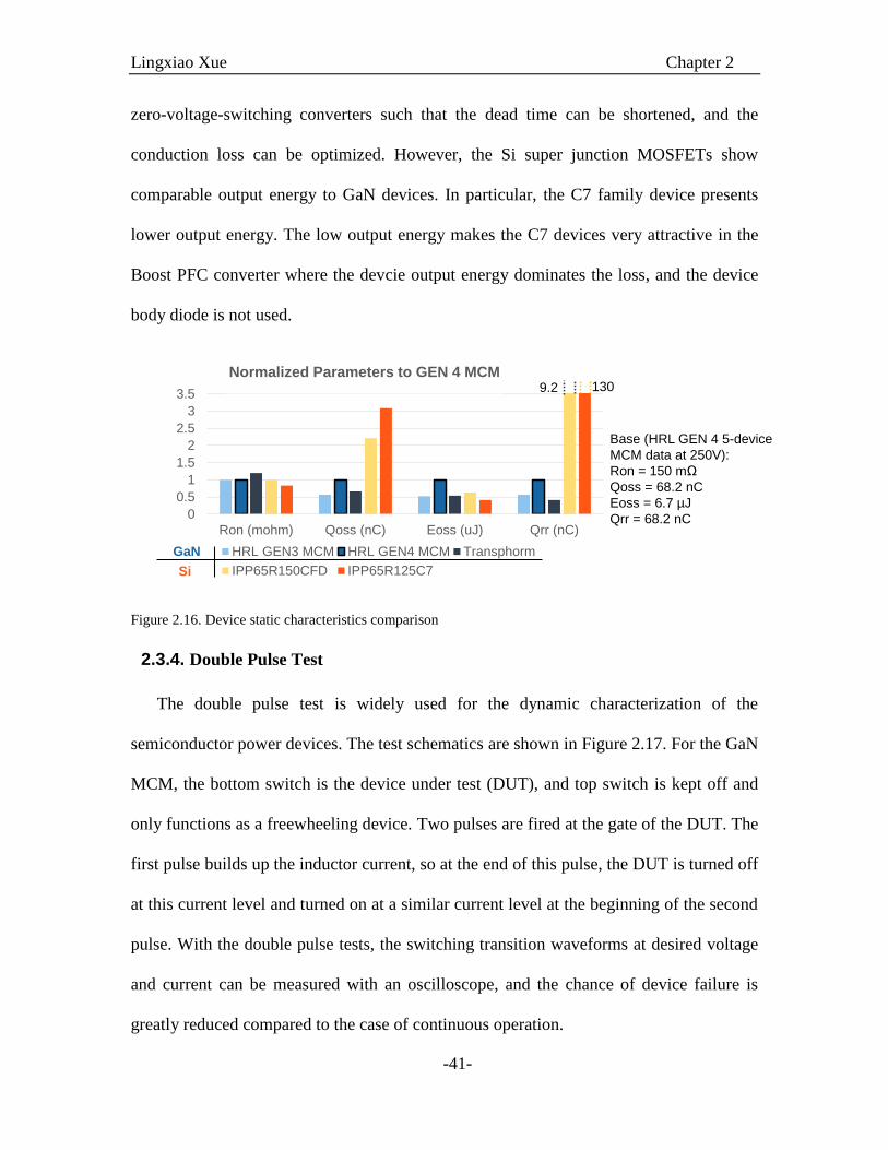
Lingxiao Xue Chapter 2
-41-
zero-voltage-switching converters such that the dead time can be shortened, and the
conduction loss can be optimized. However, the Si super junction MOSFETs show
comparable output energy to GaN devices. In particular, the C7 family device presents
lower output energy. The low output energy makes the C7 devices very attractive in the
Boost PFC converter where the devcie output energy dominates the loss, and the device
body diode is not used.
Figure 2.16. Device static characteristics comparison
2.3.4. Double Pulse Test
The double pulse test is widely used for the dynamic characterization of the
semiconductor power devices. The test schematics are shown in Figure 2.17. For the GaN
MCM, the bottom switch is the device under test (DUT), and top switch is kept off and
only functions as a freewheeling device. Two pulses are fired at the gate of the DUT. The
first pulse builds up the inductor current, so at the end of this pulse, the DUT is turned off
at this current level and turned on at a similar current level at the beginning of the second
pulse. With the double pulse tests, the switching transition waveforms at desired voltage
and current can be measured with an oscilloscope, and the chance of device failure is
greatly reduced compared to the case of continuous operation.
0
0.5
1
1.5
2
2.5
3
3.5
Ron (mohm) Qoss (nC) Eoss (uJ) Qrr (nC)
HRL GEN3 MCM HRL GEN4 MCM Transphorm
IPP65R150CFD IPP65R125C7
9.2 130Normalized Parameters to GEN 4 MCM
GaN
Si
Base (HRL GEN 4 5-device
MCM data at 250V):
Ron = 150 mΩ
Qoss = 68.2 nC
Eoss = 6.7 µJ
Qrr = 68.2 nC
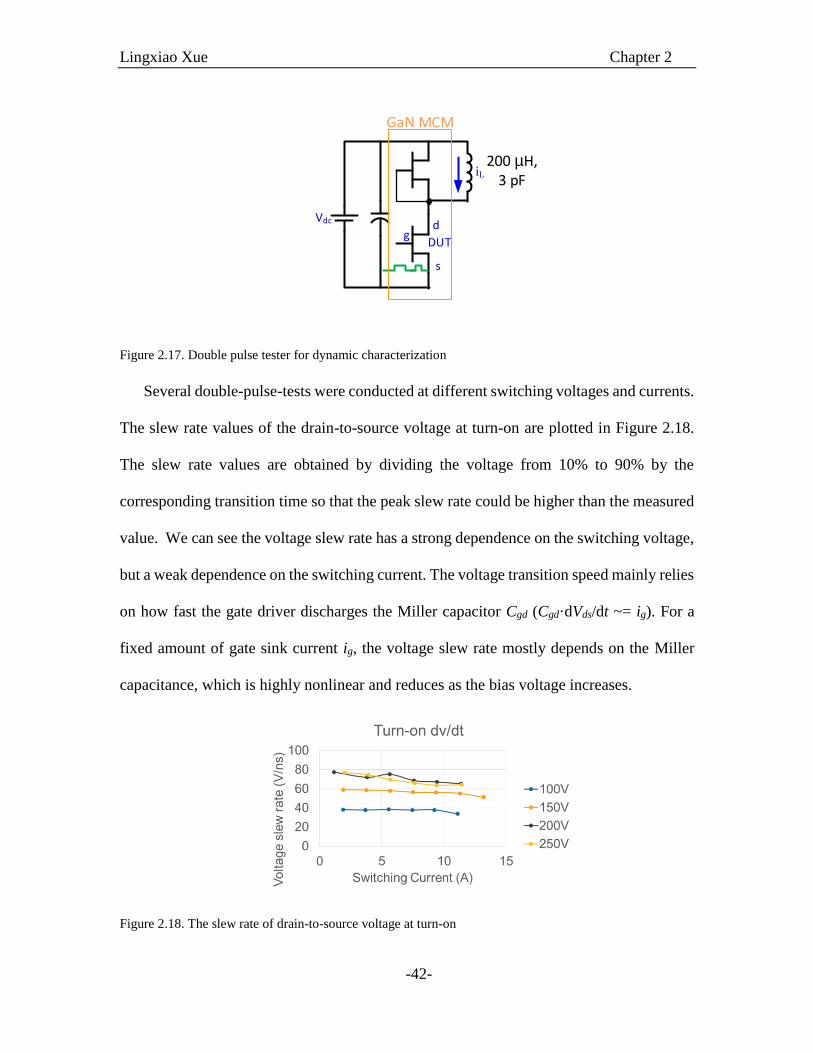
Lingxiao Xue Chapter 2
-42-
Vdc
iL
DUTg
d
s
GaN MCM
200 µH, 3 pF
Figure 2.17. Double pulse tester for dynamic characterization
Several double-pulse-tests were conducted at different switching voltages and currents.
The slew rate values of the drain-to-source voltage at turn-on are plotted in Figure 2.18.
The slew rate values are obtained by dividing the voltage from 10% to 90% by the
corresponding transition time so that the peak slew rate could be higher than the measured
value. We can see the voltage slew rate has a strong dependence on the switching voltage,
but a weak dependence on the switching current. The voltage transition speed mainly relies
on how fast the gate driver discharges the Miller capacitor Cgd (Cgd·dVds/dt ~= ig). For a
fixed amount of gate sink current ig, the voltage slew rate mostly depends on the Miller
capacitance, which is highly nonlinear and reduces as the bias voltage increases.
Figure 2.18. The slew rate of drain-to-source voltage at turn-on
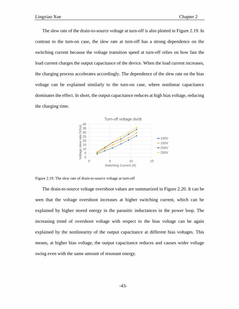
Lingxiao Xue Chapter 2
-43-
The slew rate of the drain-to-source voltage at turn-off is also plotted in Figure 2.19. In
contrast to the turn-on case, the slew rate at turn-off has a strong dependence on the
switching current because the voltage transition speed at turn-off relies on how fast the
load current charges the output capacitance of the device. When the load current increases,
the charging process accelerates accordingly. The dependence of the slew rate on the bias
voltage can be explained similarly to the turn-on case, where nonlinear capacitance
dominates the effect. In short, the output capacitance reduces at high bias voltage, reducing
the charging time.
Figure 2.19. The slew rate of drain-to-source voltage at turn-off
The drain-to-source voltage overshoot values are summarized in Figure 2.20. It can be
seen that the voltage overshoot increases at higher switching current, which can be
explained by higher stored energy in the parasitic inductances in the power loop. The
increasing trend of overshoot voltage with respect to the bias voltage can be again
explained by the nonlinearity of the output capacitance at different bias voltages. This
means, at higher bias voltage, the output capacitance reduces and causes wider voltage
swing even with the same amount of resonant energy.
0
5
10
15
20
25
30
35
40
0 5 10 15
Voltage s
lew
rate
(V
/ns)
Switching Current (A)
Turn-off voltage dv/dt
100V
150V
200V
250V
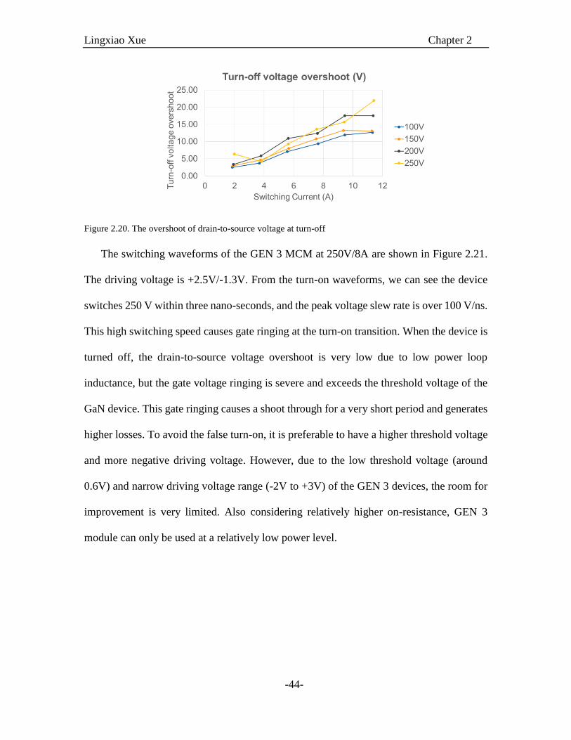
Lingxiao Xue Chapter 2
-44-
Figure 2.20. The overshoot of drain-to-source voltage at turn-off
The switching waveforms of the GEN 3 MCM at 250V/8A are shown in Figure 2.21.
The driving voltage is +2.5V/-1.3V. From the turn-on waveforms, we can see the device
switches 250 V within three nano-seconds, and the peak voltage slew rate is over 100 V/ns.
This high switching speed causes gate ringing at the turn-on transition. When the device is
turned off, the drain-to-source voltage overshoot is very low due to low power loop
inductance, but the gate voltage ringing is severe and exceeds the threshold voltage of the
GaN device. This gate ringing causes a shoot through for a very short period and generates
higher losses. To avoid the false turn-on, it is preferable to have a higher threshold voltage
and more negative driving voltage. However, due to the low threshold voltage (around
0.6V) and narrow driving voltage range (-2V to +3V) of the GEN 3 devices, the room for
improvement is very limited. Also considering relatively higher on-resistance, GEN 3
module can only be used at a relatively low power level.
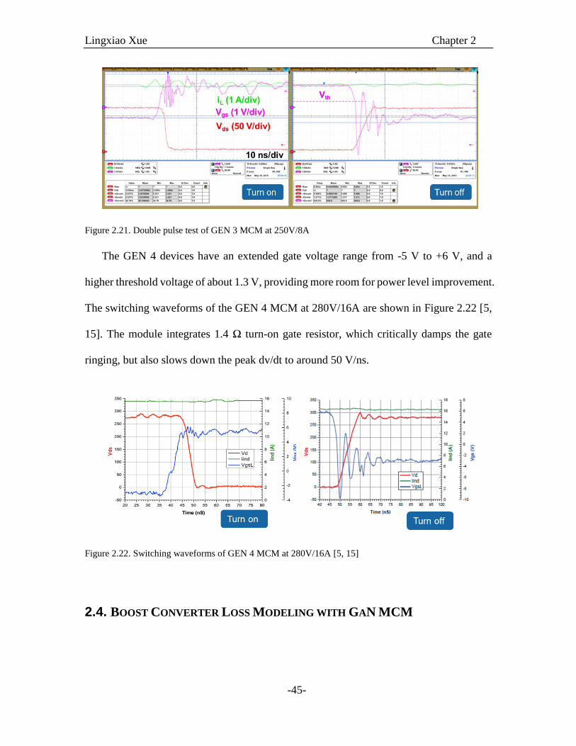
Lingxiao Xue Chapter 2
-45-
Figure 2.21. Double pulse test of GEN 3 MCM at 250V/8A
The GEN 4 devices have an extended gate voltage range from -5 V to +6 V, and a
higher threshold voltage of about 1.3 V, providing more room for power level improvement.
The switching waveforms of the GEN 4 MCM at 280V/16A are shown in Figure 2.22 [5,
15]. The module integrates 1.4 Ω turn-on gate resistor, which critically damps the gate
ringing, but also slows down the peak dv/dt to around 50 V/ns.
Figure 2.22. Switching waveforms of GEN 4 MCM at 280V/16A [5, 15]
2.4. BOOST CONVERTER LOSS MODELING WITH GAN MCM

Lingxiao Xue Chapter 2
-46-
A boost converter continuous test was conducted to exploit the potential of the GaN
MCM. The switching frequency was 500 kHz and the duty cycle was 50%. The output
voltage changed from 150 V to 250 V, and the output current was measured up to 3.5 A.
The converter waveforms at 250V and 3.5 A are shown in Figure 2.23. We can see a
very clean drain-to-source waveform due to low power loop inductance of the GaN MCM.
Figure 2.23. Boost converter test waveforms
The measured efficiency is plotted in Figure 2.24. We can see that the boost converter
achieves > 96% efficiency in the wide load range. At peak load of 250 V and 3.5 A, the
efficiency is 97.4%.
Vds (50 V/div)
iL (1 A/div)
800 ns/div
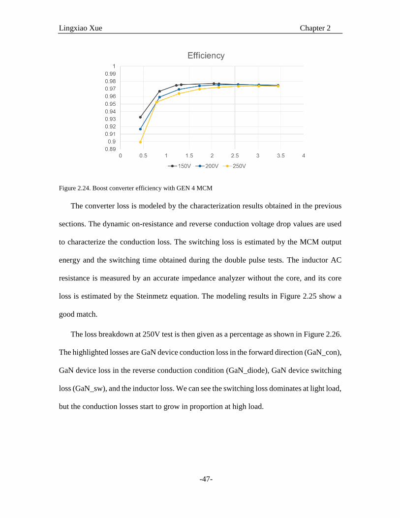
Lingxiao Xue Chapter 2
-47-
Figure 2.24. Boost converter efficiency with GEN 4 MCM
The converter loss is modeled by the characterization results obtained in the previous
sections. The dynamic on-resistance and reverse conduction voltage drop values are used
to characterize the conduction loss. The switching loss is estimated by the MCM output
energy and the switching time obtained during the double pulse tests. The inductor AC
resistance is measured by an accurate impedance analyzer without the core, and its core
loss is estimated by the Steinmetz equation. The modeling results in Figure 2.25 show a
good match.
The loss breakdown at 250V test is then given as a percentage as shown in Figure 2.26.
The highlighted losses are GaN device conduction loss in the forward direction (GaN_con),
GaN device loss in the reverse conduction condition (GaN_diode), GaN device switching
loss (GaN_sw), and the inductor loss. We can see the switching loss dominates at light load,
but the conduction losses start to grow in proportion at high load.
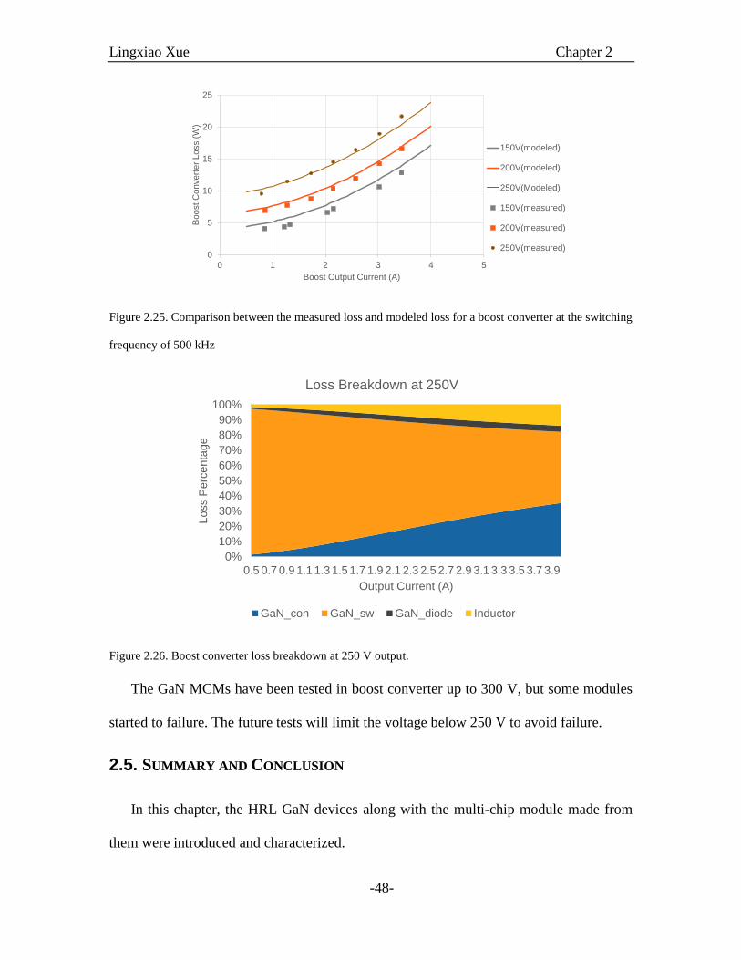
Lingxiao Xue Chapter 2
-48-
Figure 2.25. Comparison between the measured loss and modeled loss for a boost converter at the switching
frequency of 500 kHz
Figure 2.26. Boost converter loss breakdown at 250 V output.
The GaN MCMs have been tested in boost converter up to 300 V, but some modules
started to failure. The future tests will limit the voltage below 250 V to avoid failure.
2.5. SUMMARY AND CONCLUSION
In this chapter, the HRL GaN devices along with the multi-chip module made from
them were introduced and characterized.
0
5
10
15
20
25
0 1 2 3 4 5
Boo
st C
onvert
er
Loss (
W)
Boost Output Current (A)
150V(modeled)
200V(modeled)
250V(Modeled)
150V(measured)
200V(measured)
250V(measured)
0%
10%
20%
30%
40%
50%
60%
70%
80%
90%
100%
0.5 0.7 0.9 1.1 1.3 1.5 1.7 1.9 2.1 2.3 2.5 2.7 2.9 3.1 3.3 3.5 3.7 3.9
Lo
ss P
erc
en
tage
Output Current (A)
Loss Breakdown at 250V
GaN_con GaN_sw GaN_diode Inductor

Lingxiao Xue Chapter 2
-49-
The HRL GaN device technology was briefly reviewed including the key
characteristics of the GEN 3 and GEN 4 devices. GEN 4 devices have lower on-resistance,
higher threshold voltage, wider gate voltage range and higher maximum current, thereby
enable the possibility for higher power applications.
However, none of those discrete devices is sufficient for the PHEV battery charger
application, which requires multiple kilowatts of power. Furthermore, the internal and
interconnection inductances of the discrete device make high speed switching difficult.
Therefore, a multi-chip module approach is proposed to parallel multiple GaN dice for
higher current capability and at the same time, low inductances. Alternative methods were
used instead of the curve tracer method to measure the conduction characteristics of the
GaN module due to the integrated decoupling capacitors.
The dynamic on-resistance was also measured in double pulse tests as well as
continuous tests where GaN devices have been put in hard-switching and zero-voltage-
switching conditions. Results showed that double pulse tests do not present the dynamic
on-resistance phenomenon, but that continuous tests do. The devices under hard-switching
conditions shows almost doubled on-resistance at high bias voltage compared to the static
value. The zero-voltage switching case is less severe, but still an on-resistance increase can
be observed.
Output charge of the MCM was also measured in two ways, showing consistent results.
GEN 4 MCM has an almost doubled charge value of GEN 3 MCM. The output charge
measurement results can be easily manipulated to obtain the incremental capacitance (or
small signal capacitance) and the output energy. The characterizations results of the GaN
MCMs are compared with Si CoolMOS and other GaN devices. Provided the same on-
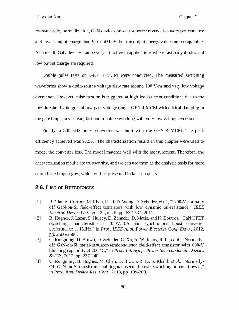
Lingxiao Xue Chapter 2
-50-
resistances by normalization, GaN devices present superior reverse recovery performance
and lower output charge than Si CoolMOS, but the output energy values are comparable.
As a result, GaN devices can be very attractive in applications where fast body diodes and
low output charge are required.
Double pulse tests on GEN 3 MCM were conducted. The measured switching
waveforms show a drain-source voltage slew rate around 100 V/ns and very low voltage
overshoot. However, false turn-on is triggered at high load current conditions due to the
low threshold voltage and low gate voltage range. GEN 4 MCM with critical damping in
the gate loop shows clean, fast and reliable switching with very low voltage overshoot.
Finally, a 500 kHz boost converter was built with the GEN 4 MCM. The peak
efficiency achieved was 97.5%. The characterization results in this chapter were used to
model the converter loss. The model matches well with the measurement. Therefore, the
characterization results are trustworthy, and we can use them as the analysis basis for more
complicated topologies, which will be presented in later chapters.
2.6. LIST OF REFERENCES
[1] R. Chu, A. Corrion, M. Chen, R. Li, D. Wong, D. Zehnder, et al., "1200-V normally
off GaN-on-Si field-effect transistors with low dynamic on-resistance," IEEE
Electron Device Lett., vol. 32, no. 5, pp. 632-634, 2011.
[2] B. Hughes, J. Lazar, S. Hulsey, D. Zehnder, D. Matic, and K. Boutros, "GaN HFET
switching characteristics at 350V/20A and synchronous boost converter
performance at 1MHz," in Proc. IEEE Appl. Power Electron. Conf. Expo., 2012,
pp. 2506-2508.
[3] C. Rongming, D. Brown, D. Zehnder, C. Xu, A. Williams, R. Li, et al., "Normally-
off GaN-on-Si metal-insulator-semiconductor field-effect transistor with 600-V
blocking capability at 200 oC," in Proc. Int. Symp. Power Semiconductor Devcies
& IC's, 2012, pp. 237-240.
[4] C. Rongming, B. Hughes, M. Chen, D. Brown, R. Li, S. Khalil, et al., "Normally-
Off GaN-on-Si transistors enabling nanosecond power switching at one kilowatt,"
in Proc. Ann. Device Res. Conf., 2013, pp. 199-200.
Lingxiao Xue Chapter 2
-51-
[5] B. Hughes, C. Rongming, J. Lazar, S. Hulsey, A. Garrido, D. Zehnder, et al.,
"Normally-off GaN switching 400V in 1.4ns using an ultra-low resistance and
inductance gate drive," in Proc. IEEE Workshop on Wide Bandgap Power Devices
and Appl., 2013, pp. 76-79.
[6] L. Fang, C. Zheng, X. Lingxiao, P. Mattavelli, D. Boroyevich, and B. Hughes,
"Design considerations for GaN HEMT multichip halfbridge module for high-
frequency power converters," in Proc. IEEE Appl. Power Electron. Conf. Expo.,
2014, pp. 537-544.
[7] D. Reusch, F. C. Lee, D. Gilham, and S. Yipeng, "Optimization of a high density
gallium nitride based non-isolated point of load module," in Proc. IEEE Energy
Convers. Congr. Expo., 2012, pp. 2914-2920.
[8] B. Hughes, J. Lazar, S. Hulsey, M. Musni, D. Zehnder, A. Garrido, et al.,
"Normally-off GaN-on-Si multi-chip module boost converter with 96% efficiency
and low gate and drain overshoot," in Proc. IEEE Appl. Power Electron. Conf.
Expo., 2014, pp. 484-487.
[9] M. T. Hasan, "Mechanism and Suppression of Current Collapse in AlGaN/GaN
High Electron Mobility Transistors," Ph.D. dissertation, University of Fukui, 2013.
[10] W. Saito, T. Noda, M. Kuraguchi, Y. Takada, K. Tsuda, Y. Saito, et al., "Effect of
Buffer Layer Structure on Drain Leakage Current and Current Collapse Phenomena
in High-Voltage GaN-HEMTs," IEEE Trans. Electron. Devices, vol. 56, no. 7, pp.
1371-1376, 2009.
[11] W. Saito, T. Nitta, Y. Kakiuchi, Y. Saito, T. Noda, H. Fujimoto, et al., "Influence
of electric field upon current collapse phenomena and reliability in high voltage
GaN-HEMTs," in Proc. IEEE Int. Rel. Physics Symp., 2010, pp. 339-342.
[12] J. Donghyun and J. A. del Alamo, "Methodology for the Study of Dynamic ON-
Resistance in High-Voltage GaN Field-Effect Transistors," IEEE Trans. Electron.
Devices, vol. 60, no. 10, pp. 3190-3196, 2013.
[13] Y. Nozaki, H. Kawamura, J. K. Twynam, and M. Hasegawa, "Voltage clamp circuit
and semiconductor device, overcurrent protection circuit, voltage measurement
probe, voltage measurement device and semiconductor evaluation device
respectively using the same," ed: Google Patents, 2008.
[14] R. Elferich, "General ZVS half bridge model regarding nonlinear capacitances and
application to LLC design," in Proc. IEEE Energy Convers. Congr. Expo., 2012,
pp. 4404-4410.
[15] B. Hughes. Normally-Off GaN-on-Si Bi-Directional Automobile Battery-to -Grid
6.6kW Charger Switching at 500kHz. presented at 2014 Appl. Power Electron.
Conf. Expo. [Online]. Available: http://www.apec-conf.org/wp-
content/uploads/IS2-4-5.pdf

Lingxiao Xue Chapter 3
-52-
Chapter 3. BATTERY CHARGER TOPOLOGY EVALUATION
Equation Chapter (Next) Section 1The bi-directional battery charger is used to process
power between the AC utility grid side and the DC PHEV battery side. A typical Level 2
battery charger can deliver 6.6 kW maximum power to the battery pack whose voltage
ranges from 270 V to 430 V. Furthermore, the battery charger should be able to achieve
high power factor at the AC side and enforce a predetermined charging profile at the battery
side with different charging modes including constant current, constant power, and
constant voltage. Topologies that can complete those tasks should be considered. We will
not consider the integrated charger and inductive/wireless charging schemes due to the
reason explained in Chapter 1. The topology selection also take account the implementation
of GaN devices.
3.1. TOPOLOGY ARCHITECTURE
3.1.1. Isolated or Non-isolated Topologies
The charger could either be non-isolated or isolated. Compared to isolated chargers that
require transformers, non-isolated chargers have the advantages of simple structure, low
cost, low size and weight, and also high efficiency. Some early research on bi-directional
chargers adopted the non-isolated solutions [1-4]. A non-isolated topology mainly consists
of an AC/DC stage and a non-isolated DC/DC stage. The non-isolated stage can be a half-
bridge converter, Cuk converter, or SEPIC/Luo Converter, but the half-bridge converter
turns out to be the best candidate [5]. Some half-bridge-based topologies, such as cascade
half-bridge converter, interleaved half-bridge converter, and three-level converters, have
been proposed to reduce loss and device stress [3, 5, 6].

Lingxiao Xue Chapter 3
-53-
However, galvanic isolation is strongly preferable. The vehicle body must be grounded
to the earth while charging for safety considerations. Therefore, if the charger provides no
isolation between the grid and the battery, shielding and safety issues should be thoroughly
considered to keep the battery isolated from the EV body and prevent an unwanted earth
fault protection trip [7]. As an alternative, a line frequency transformer can be used to
achieve the isolation between the grid and the battery, but it will be very bulky and
expensive. Therefore, it is more convenient to integrate the galvanic isolation into the
battery charger. Furthermore, isolation transformers can facilitate voltage step-down or
step-up to maintain optimized duty cycle of the semiconductor switches. As a result, most
of the recently reported battery chargers adopt isolated topologies.
3.1.2. Single-Stage, Quasi-Single-Stage, and Two-Stage Topologies
The topology of an isolated bi-directional battery charger is illustrated by the diagram
in Figure 3.1. To save volume, weight and cost, a high frequency (HF) transformer is used.
In the charging mode, the AC side conversion block before the transformer needs to chop
the line frequency (LF) AC voltage into a high frequency (HF) AC voltage, which is then
rectified by the DC side block into a DC battery voltage. By controlling the two conversion
blocks, the power factor correction and charging profile can be enforced.
When each conversion block in Figure 3.1 is realized by one directly conversion stage,
the corresponding topologies are classified as single-stage topology. Bi-directional, single-
stage, isolated converters can be found in [8-15]. The topology diagrams of those
converters are listed in Figure 3.2. In contrast, a two-stage solution typically has two
cascaded stages to realize the AC/AC conversion.

Lingxiao Xue Chapter 3
-54-
AC GridBatteryLF
AC
HF
AC
HF
AC
DC
VacVbatt
Iac
Figure 3.1. Topology block diagram of an isolated bi-directional charging system
(a) Dual full bridge (b) Push-pull
(c) Current-fed dual full bridge (d) Dual full bridge with LC network
(e) Dual full bridge with LCL network (f) Half bridge plus full bridge
Figure 3.2. Topologies of single-stage, bi-directional, isolated AC/DC converter
The direct AC/AC converter requires four-quadrant switches that can block voltage and
conduct current in both directions. That is why in Figure 3.2, two two-quadrant switches
in anti-series are used to build one four-quadrant switch. As shown, the AC/DC conversion
stage between the transformer and the battery are all simple full bridges for all six
topologies. The main differences are at the AC side. In [13, 15, 16], a full bridge with four-

Lingxiao Xue Chapter 3
-55-
quadrant switches is used, as shown in Figure 3.2(a). The AC side switches are driven with
fixed 50% duty cycle. The AC side current is proportional to the duty cycle of the DC side
switches; therefore, power factor correction can be naturally achieved without a control
loop. The average delivered power depends on the applied phase shift between the AC side
and DC side. ZVS and ZCS are achieved at the DC side and AC side, respectively.
However, the peak efficiency is slightly lower than 90% from 1.2 kW to 1.4 kW. A four-
step current commutation is implemented to prevent device failure due to lack of current
freewheeling path. A similar topology with a push-pull AC side is proposed by the same
group, as shown in Figure 3.2(b) [10]. The topology has the same benefits, but no
experimental results were reported.
To target high efficiency and high frequency, ZVS for the AC side is preferable.
However, the nature of ZVS requires the current to freewheel in the reverse direction of
the AC side switch, which conflicts with the configuration of the four-quadrant switches
that inherently block the reverse current if not gated. Reference [8] (topology shown in
Figure 3.2(c)) claimed either zero-voltage or zero-current switching conditions can be
achieved for all the switches, but the commutation sequence control requires complicated
finite state machine and auxiliary circuitry for switch voltage feedback. Zero-voltage
switching at the AC side switches can also be achieved by inserting a resonant tank between
the bridge and the transformer [9, 12], as shown in Figure 3.2(d) and Figure 3.2(e). The
converters still use constant frequency, and the power transfer depends on the duty cycle
of the two bridges and phase shift between the two bridges. However, the AC side ZVS
conditions still require the two switches in the four-quadrant switch being controlled
individually. Reference [11] used the half-bridge version of Figure 3.2(a), as shown in
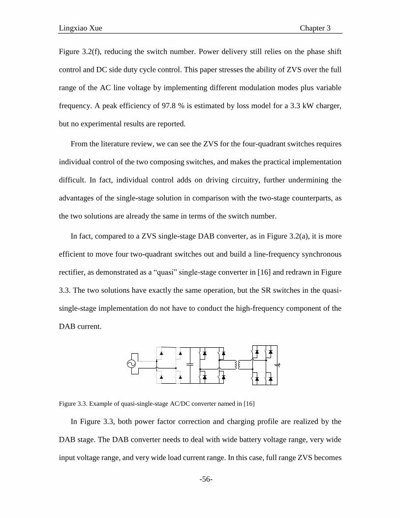
Lingxiao Xue Chapter 3
-56-
Figure 3.2(f), reducing the switch number. Power delivery still relies on the phase shift
control and DC side duty cycle control. This paper stresses the ability of ZVS over the full
range of the AC line voltage by implementing different modulation modes plus variable
frequency. A peak efficiency of 97.8 % is estimated by loss model for a 3.3 kW charger,
but no experimental results are reported.
From the literature review, we can see the ZVS for the four-quadrant switches requires
individual control of the two composing switches, and makes the practical implementation
difficult. In fact, individual control adds on driving circuitry, further undermining the
advantages of the single-stage solution in comparison with the two-stage counterparts, as
the two solutions are already the same in terms of the switch number.
In fact, compared to a ZVS single-stage DAB converter, as in Figure 3.2(a), it is more
efficient to move four two-quadrant switches out and build a line-frequency synchronous
rectifier, as demonstrated as a “quasi” single-stage converter in [16] and redrawn in Figure
3.3. The two solutions have exactly the same operation, but the SR switches in the quasi-
single-stage implementation do not have to conduct the high-frequency component of the
DAB current.
Figure 3.3. Example of quasi-single-stage AC/DC converter named in [16]
In Figure 3.3, both power factor correction and charging profile are realized by the
DAB stage. The DAB converter needs to deal with wide battery voltage range, very wide
input voltage range, and very wide load current range. In this case, full range ZVS becomes

Lingxiao Xue Chapter 3
-57-
very challenging to achieve. The parameters of the DAB modulation modes are difficult to
be computed online, so they are obtained from a lookup table that is only good for one
converter. Considering a high-frequency GaN converter where DSP calculation time must
be minimized, this solution should be avoided.
To summarize, the single-stage solutions, although they might be the most intuitive,
have the following drawbacks:
1. It is difficult to achieve ZVS for the AC side switches. A complicated commutation
sequence with ZVS consideration requires individual control of the switches that comprise
the four-quadrant switch. Without sharing drives, the driving circuit number, in this case,
is the same as that of the two-stage solution, as both solutions have the same number of
switches. Furthermore, the commutation sequence in a single-stage solution is more
complex.
2. It is difficult to optimize the converter under wide operating conditions. The single-
stage converter has to take into account the wide voltage and current range at both input
and output, so the converter is very difficult to optimize within this wide range. This
argument also applies to the quasi-single-stage converter.
3. It is difficult to control the ripple current to the battery pack. For both single-stage
and quasi-single-stage converters, there are no intermediate energy storages for double line
frequency power, so the power is directly passed to the DC side without control. The ripple
current to the battery can only be suppressed by passively paralleling capacitors to the
battery pack. The filtering effect of this paralleled capacitor strongly depends on the
impedance of the battery pack. In contrast, the same capacitors placed at the DC link of a
two-stage converter are more effective at absorbing the ripple, because the following

Lingxiao Xue Chapter 3
-58-
DC/DC stage can be controlled to show high impedance at the double line frequency. As
we will see in Chapter 4, the two-stage solution facilitates the control of ripple power to
the battery in terms of amplitude and shape.
4. The single-stage solution does not necessarily improve power density. First, single-
stage converters do not save on switch number because four-quadrant switches are not
available and must be built from two two-quadrant switches. If the switches are
individually controlled, the driving circuitry saving is also lost. Second, single-stage is not
the only solution to save in terms of DC link volume. As we will show in Chapter 4,
theoretically, a two-stage solution can also eliminate the DC link capacitors.
Therefore, in this work, two-stage topology will be selected due to high flexibility and
easier optimization with respect to conversion efficiency. For this solution, the AC/AC
conversion is realized by cascading an AC/DC stage and DC/AC stage that are decoupled
by a DC link, as shown in Figure 3.4. The DC/AC conversion block is closely linked by
the transformer to the right-side AC/DC stage, and therefore is usually regarded as one
isolated DC/DC converter. As a result, a typical two-stage topology consists of a non-
isolated AC/DC front-end converter and an isolated DC/DC converter. In most cases, the
two stages are decoupled by the DC link, and the AC/DC converter regulates the DC link
voltage and correct the power factor while the DC/DC converter enforces the charging
profile. Thus, the topology selection of a two-stage solution can be split into two problems:
the AC/DC front end converter selection and the isolated DC/DC converter selection,
which will be covered in section 3.2.1 and section 3.2.2, respectively.

Lingxiao Xue Chapter 3
-59-
AC GridBattery
DC
HF
AC
HF
AC
DC
VacVbatt
Iac
LF
AC
DC
AC/DC
Front End
Isolated
DC/DC
Figure 3.4. Topology diagram of an isolated two-stage solution with a non-isolated AC/DC converter plus
an isolated DC/DC converter
3.2. TWO-STAGE ISOLATED TOPOLOGY SURVEY
3.2.1. AC/DC Stage
The non-isolated AC/DC topologies with power factor correction capability have been
intensively reviewed in [17, 18]. AC/DC topologies suitable to the electric vehicle charger
are reviewed in [19-21]. The most promising and widely adopted topologies of AC/DC
front end that allow for bi-directional power flow are listed in Figure 3.5.
Full bridge, as shown in Figure 3.5 (a) is the most popular topology widely reported in
literature [1, 3, 22-24]. This topology can be derived from a bridgeless PFC converter by
replacing the diodes with active switches, so bi-directional power flow can be achieved.
Therefore, the converter is inherently a boost converter in rectifier mode, and the switching
patterns follow the basic cycles of inductor-charging and energy-transfer. Accordingly, the
output DC voltage should be higher than the AC voltage peak in normal operation due to
the boost converter nature. Various modulation methods can be used to optimize different
performance indices, such as converter loss, EMI noise and filter size [25]. For example,
unipolar modulation can double the equivalent ripple current frequency with the same
switching frequency so that the boost inductance could be halved. With discontinuous
PWM modulation, each switch could stay off for half of the line cycle so that the overall
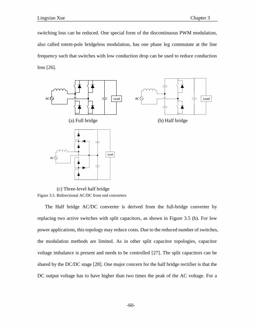
Lingxiao Xue Chapter 3
-60-
switching loss can be reduced. One special form of the discontinuous PWM modulation,
also called totem-pole bridgeless modulation, has one phase leg commutate at the line
frequency such that switches with low conduction drop can be used to reduce conduction
loss [26].
AC Load
AC Load
(a) Full bridge (b) Half bridge
ACLoad
(c) Three-level half bridge
Figure 3.5. Bidirectional AC/DC front end converters
The Half bridge AC/DC converter is derived from the full-bridge converter by
replacing two active switches with split capacitors, as shown in Figure 3.5 (b). For low
power applications, this topology may reduce costs. Due to the reduced number of switches,
the modulation methods are limited. As in other split capacitor topologies, capacitor
voltage imbalance is present and needs to be controlled [27]. The split capacitors can be
shared by the DC/DC stage [28]. One major concern for the half bridge rectifier is that the
DC output voltage has to have higher than two times the peak of the AC voltage. For a

Lingxiao Xue Chapter 3
-61-
universal AC input application, this usually means around 800 V DC bus. High
performance 650 V MOSFETs cannot be used.
The three level AC/DC converter, as shown in Figure 3.5 (c), can reduce the switch
voltage stress to half of the DC bus voltage [29]. More variations of the three level
converter can be found in [30]. Although the active switch number is the same as the full
bridge solution, those auxiliary components, such as clamping diodes and capacitors mean
additional cost.
In summary, the half bridge (HB) solution has too much voltage stress, so the 600 V
GaN module cannot be used. The 3-level half bridge converter requires two large
capacitors and balancing control that may hurt the power density. Finally, as a result, the
full bridge topology is chosen for the front end AC/DC converter.
3.2.2. Isolated DC/DC Stage
The isolated bi-directional DC/DC converters have been reviewed in [31], [32]and [33].
The architecture of an isolated DC/DC converter is depicted in Figure 3.6.
DC linkBattery
FilterLC
Network
DC
HF
AC
LC
Network
HF
AC
DC
Filter
Figure 3.6. Topology architecture of an isolated bi-directional DC/DC converter
The filters at both sides smooth terminal voltages and currents. In the simplest case, the
filter can be a capacitor or an inductor, which leads to a voltage-fed or a current-fed
topology. The filters are directly connected to the switch network, which accomplishes DC
to AC conversion or AC to DC conversion. The LC networks are comprised of inductors
and capacitors that handle energy transfer or provide circulating energy to optimize

Lingxiao Xue Chapter 3
-62-
switching transition. The LC network could contain a simple inductor for some topologies
or complicated resonant components for other topologies.
In a voltage-fed topology, the switch voltages in a phase-leg are always clamped to the
DC bus voltage by the paralleled capacitor, but in a current-fed topology, voltage ringing
is much more serve due to lack of clamping. For PHEV battery charger applications, both
the DC link voltage and the battery voltage are in the range of hundreds of volts. Therefore,
a very high voltage spike could occur if current-fed filters are used. The high switching
di/dt of the GaN transistors will make the voltage spike worse. As GaN transistors do not
have avalanche breakdown capability, the occurrence of over-voltage is destructive.
Therefore, only voltage-fed topologies will be considered in this work.
The DC to HF AC conversion stage can be realized by the full bridge, half bridge, push-
pull or L-type HB, as reviewed in [31]. Switches in the push-pull and L-type HB converters
are not in a phase-leg configuration, so the switch voltages are not clamped to the DC bus.
Therefore, a high voltage spike may occur due to the transformer leakage inductance, and
worsen when GaN devices are used. In general, push-pull and L-type HB topologies are
more suitable for low voltage, high current applications.
Full bridge and half bridge converters are beneficial in this sense. The switch voltages
are all clamped to the DC rails. The power loop can be optimized by placing decoupling
capacitors very close to the phase leg, resulting in a very small parasitic inductance, and
enabling reliable switching. The half bridge converter can only output half the DC bus
voltage, so if the same power is delivered, the output current and switch current will be
doubled. Accordingly, this increases the conduction loss for both the magnetic components
and the semiconductor switches. Therefore, the full bridge converter is preferred.
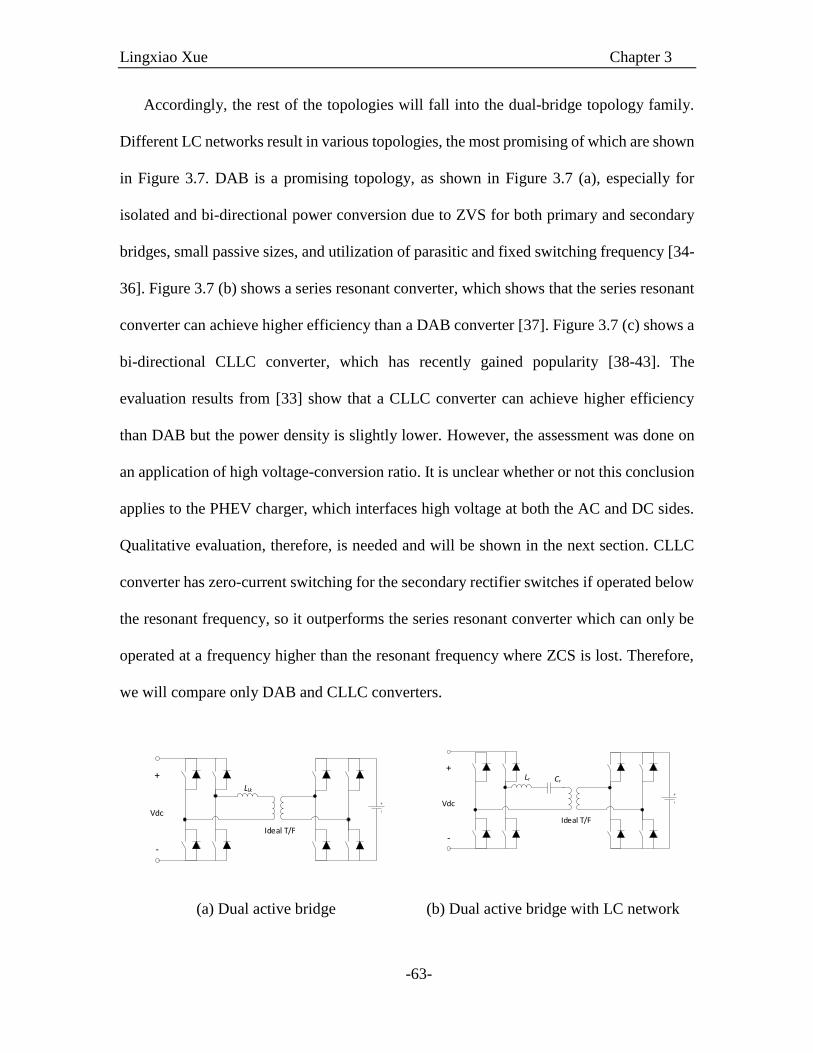
Lingxiao Xue Chapter 3
-63-
Accordingly, the rest of the topologies will fall into the dual-bridge topology family.
Different LC networks result in various topologies, the most promising of which are shown
in Figure 3.7. DAB is a promising topology, as shown in Figure 3.7 (a), especially for
isolated and bi-directional power conversion due to ZVS for both primary and secondary
bridges, small passive sizes, and utilization of parasitic and fixed switching frequency [34-
36]. Figure 3.7 (b) shows a series resonant converter, which shows that the series resonant
converter can achieve higher efficiency than a DAB converter [37]. Figure 3.7 (c) shows a
bi-directional CLLC converter, which has recently gained popularity [38-43]. The
evaluation results from [33] show that a CLLC converter can achieve higher efficiency
than DAB but the power density is slightly lower. However, the assessment was done on
an application of high voltage-conversion ratio. It is unclear whether or not this conclusion
applies to the PHEV charger, which interfaces high voltage at both the AC and DC sides.
Qualitative evaluation, therefore, is needed and will be shown in the next section. CLLC
converter has zero-current switching for the secondary rectifier switches if operated below
the resonant frequency, so it outperforms the series resonant converter which can only be
operated at a frequency higher than the resonant frequency where ZCS is lost. Therefore,
we will compare only DAB and CLLC converters.
+
-
Vdc
Ideal T/F
Llk
+
-
Vdc
Ideal T/F
Lr Cr
(a) Dual active bridge (b) Dual active bridge with LC network

Lingxiao Xue Chapter 3
-64-
+
-
Vdc
CrIdeal T/F
Lr
Lm
Crs
Lrs
(c) CLLC resonant converter
Figure 3.7. Full-bridge-based bi-directional isolated DC/DC converters
In some paper, the isolated DC/DC stage is again realized by cascading two stages
including an unregulated isolated DC/DC plus a regulated buck boost stage [37, 44]. In this
case, the unregulated isolated stage is optimized as a DC transformer (DCX) so high
efficiency can be achieved. The cascaded buck/boost converter is used to regulate the
output.
3.3. EVALUATION OF THE CANDIDATE TOPOLOGIES
In this section, candidate topologies will be evaluated and compared. For the AC/DC
stage, the full bridge topology will be evaluated by using different modulation schemes.
For the DC/DC stage, dual active bridge and CLLC resonant converters will be compared.
3.3.1. AC/DC Stage: CCM modulation and TCM modulation
As mentioned, the totem-pole modulation for the full bridge can reduce switching loss
and the conduction loss. Conventionally, continuous conduction mode (CCM) is used for
high power converters due to low current stress, but the switching frequency is low due to
hard-switching loss. Critical conduction mode (CRM) reduces the switching loss by
turning off the switch at the zero crossing of the inductor current and turning on the
complementary switch at the resonant valley of the drain-source voltage [45]. Therefore,
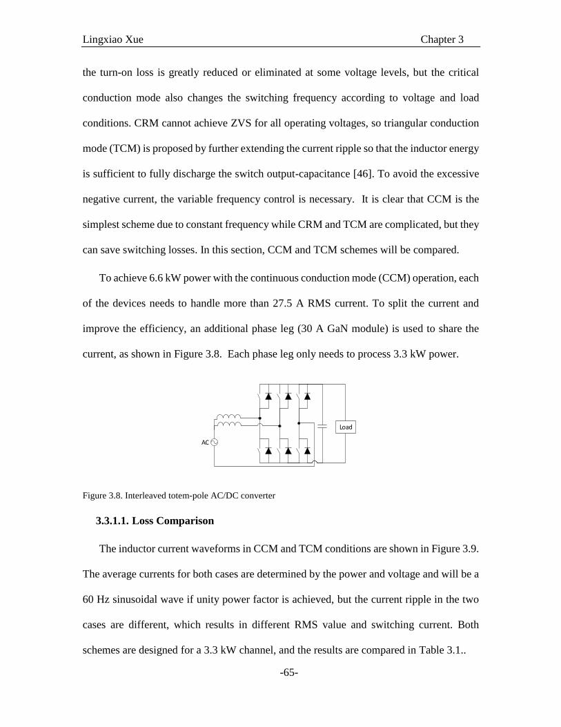
Lingxiao Xue Chapter 3
-65-
the turn-on loss is greatly reduced or eliminated at some voltage levels, but the critical
conduction mode also changes the switching frequency according to voltage and load
conditions. CRM cannot achieve ZVS for all operating voltages, so triangular conduction
mode (TCM) is proposed by further extending the current ripple so that the inductor energy
is sufficient to fully discharge the switch output-capacitance [46]. To avoid the excessive
negative current, the variable frequency control is necessary. It is clear that CCM is the
simplest scheme due to constant frequency while CRM and TCM are complicated, but they
can save switching losses. In this section, CCM and TCM schemes will be compared.
To achieve 6.6 kW power with the continuous conduction mode (CCM) operation, each
of the devices needs to handle more than 27.5 A RMS current. To split the current and
improve the efficiency, an additional phase leg (30 A GaN module) is used to share the
current, as shown in Figure 3.8. Each phase leg only needs to process 3.3 kW power.
AC
Load
Figure 3.8. Interleaved totem-pole AC/DC converter
3.3.1.1. Loss Comparison
The inductor current waveforms in CCM and TCM conditions are shown in Figure 3.9.
The average currents for both cases are determined by the power and voltage and will be a
60 Hz sinusoidal wave if unity power factor is achieved, but the current ripple in the two
cases are different, which results in different RMS value and switching current. Both
schemes are designed for a 3.3 kW channel, and the results are compared in Table 3.1..

Lingxiao Xue Chapter 3
-66-
Iavg Iavg
iLiLTCMCCM
Figure 3.9. Inductor current waveforms in CCM and TCM conditions
Table 3.1. Electric characteristics of one 3.3 kW phase with CCM and TCM modulations
CCM TCM
AC Side Voltage (V) 240 240
Output DC Voltage (V) 400 400
Inductance (µH) 30 2.65
Switching Frequency (MHz) 0.5 0.5 - 3.3
RMS Current (A) 13.8 15.9
Peak Switching Current (A) 21.2 38.9
GaN Conduction Loss (W) 30.2 40.0
GaN Switching Loss (W) 35.1 ~ 0
Both cases are designed with 240 V AC and 400 V DC. The switching frequency of
the CCM case is selected as 500 kHz, and the AC inductance is selected as a 30 µH
inductance brings the current ripple around 15% of its average value after interleaving. For
the TCM, the selected AC inductance is 2.65 µH so that the lowest switching frequency is
also 500 kHz. In this case, both CCM and TCM have the similar dominant frequency for
EMI filter design.
The TCM modulation has higher RMS current level compared to the CCM modulation
due to the increased current ripple. Accordingly, the GaN conduction loss increased by
around 30%. Meanwhile, CCM suffers from the high switching loss at the switch turn-on
while TCM eliminates the turn-on loss by ZVS. For the HRL GaN module, since the turn-
off loss is almost negligible compared to the turn-on loss, the TCM modulation results in
Lingxiao Xue Chapter 3
-67-
very low switching loss. However, it is worth mentioning that with nearly doubled turn-off
current in case of TCM (38.9 A versus 21.2 A in CCM), the chance of false turn-on
increases due to common-source inductance and Miller capacitance increases.
The inductor design considerations for the two modulation methods are very different.
For the CCM case, the peak flux density is constrained by the peak current because the
core loss is low due to small current ripple. In contrast, for the TCM case, the peak flux
density is limited by the core loss. For winding loss, from Table 3.1., we can see that the
RMS current is higher for the TCM modulation. More importantly, the switching-
frequency components are much higher, which usually leads to higher winding loss
because the high-frequency resistance can be several times of the DC value. However, we
cannot conclude which modulation is more advantageous in loss before going through the
physical design and optimization. In [47], a 1.2 kW, 1 MHz, CRM inductor shows 2.8 W
total loss. In [48], a pair of 3.3 kW, 500 kHz, CCM inductors show 4.5 W total loss. By
scaling up the 1.2 kW inductor to 3.3 kW and scaling down the switching frequency, we
can see the two modulation methods have comparable total losses. Compared to the GaN-
related loss, the inductor loss is not dominant.
3.3.1.2. Modulation Realization
The TCM modulation is derived from the critical conduction mode (CRM) modulation.
CRM provides no negative current while TCM modulation increases the current ripple to
generate a negative current that provides just sufficient energy for ZVS purpose. Further
increasing the negative current causes more circulating energy and increases the
conduction loss. The amount of negative current can be modified by controlling the on-
time of the synchronous-rectifier switch. However, it is difficult to decide this on-time with
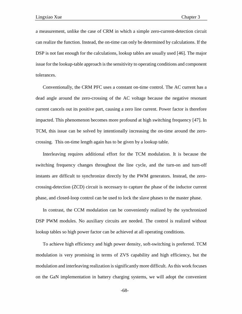
Lingxiao Xue Chapter 3
-68-
a measurement, unlike the case of CRM in which a simple zero-current-detection circuit
can realize the function. Instead, the on-time can only be determined by calculations. If the
DSP is not fast enough for the calculations, lookup tables are usually used [46]. The major
issue for the lookup-table approach is the sensitivity to operating conditions and component
tolerances.
Conventionally, the CRM PFC uses a constant on-time control. The AC current has a
dead angle around the zero-crossing of the AC voltage because the negative resonant
current cancels out its positive part, causing a zero line current. Power factor is therefore
impacted. This phenomenon becomes more profound at high switching frequency [47]. In
TCM, this issue can be solved by intentionally increasing the on-time around the zero-
crossing. This on-time length again has to be given by a lookup table.
Interleaving requires additional effort for the TCM modulation. It is because the
switching frequency changes throughout the line cycle, and the turn-on and turn-off
instants are difficult to synchronize directly by the PWM generators. Instead, the zero-
crossing-detection (ZCD) circuit is necessary to capture the phase of the inductor current
phase, and closed-loop control can be used to lock the slave phases to the master phase.
In contrast, the CCM modulation can be conveniently realized by the synchronized
DSP PWM modules. No auxiliary circuits are needed. The control is realized without
lookup tables so high power factor can be achieved at all operating conditions.
To achieve high efficiency and high power density, soft-switching is preferred. TCM
modulation is very promising in terms of ZVS capability and high efficiency, but the
modulation and interleaving realization is significantly more difficult. As this work focuses
on the GaN implementation in battery charging systems, we will adopt the convenient

Lingxiao Xue Chapter 3
-69-
CCM modulation. Some interesting phenomena obtained from the converter also apply to
the TCM case, as will be introduced in the later chapters. Efficiency and power density
improvement by using TCM modulation should be explored in future work.
3.3.2. DC/DC Stage: DAB and CLLC Resonant Converter
To limit the peak power of each GaN module and achieve high efficiency, two channels
are again used for the full 6.6 kW power. In this case, either DAB or the CLLC resonant
converter will be designed for 3.3 kW power. In both designs, we assume the input voltage
from the DC link is 350 V, and a simple charging profile is defined to deliver 3.3 kW
constant power from 270 V to 430 V battery voltages. Also, DC current charging is
assumed.
The DAB switching frequency is 500 kHz. The DAB transformer turns ratio is selected
to be 1:1. The DAB inductance is designed based on the converter loss. The DAB
semiconductor loss at different battery voltages is plotted in Figure 3.10. The loss is derived
by the analytical model derived in Section 5.3.3. The DAB loss shows a “U”-shape because
at too high or too low battery voltages, DAB falls into the hard-switching region, as will
be described in Section 5.3.2.2. We can also see that bigger commutation inductance leads
to lower loss both at the low and high battery voltages, mainly due to extended ZVS range,
but increases the loss at the middle range of the battery voltages because of increased
circulating energy. Based on the overall charging profile, an optimal commutation
inductance value can be determined [49].

Lingxiao Xue Chapter 3
-70-
Figure 3.10. DAB total semiconductor loss at different battery voltages and commutation inductance.
The CLLC resonant converter needs to be designed to accommodate the wide battery
voltage range following the procedure in [40]. There are five resonant components in this
topology. To ensure symmetrical gain in the bi-directional power flow, the LC resonant
tank at the secondary side, after referred to the primary side, should be the same to the
resonant tank of the primary side. Therefore, there are only three independent resonant
components to design, namely, the magnetizing inductance Lm, the resonant inductor Lr,
and the resonant capacitor Cr.
The magnetizing inductance is selected to provide sufficient but not excessive
circulating energy for ZVS purpose. Too small magnetizing inductance increases the
conduction loss, and too high value leads to longer dead time. Considering the output
capacitance of HRL GaN MCM, an inductance value of 33 µH is selected and the
corresponding dead time is 40 ns. The other two components are designed according to the
gain curve of the CLLC converters as shown in Figure 3.11. The curves are obtained from
simulations for better accuracy instead of analytical expressions based on the fundamental
harmonic assumption (FHA). Each curve corresponds to one equivalent load resistance
determined by the battery voltage and the power (Ro=Po/Vb). This curve shows the possible
0
20
40
60
80
100
120
140
160
180
270 290 310 330 350 370 390 410 430D
AB
Lo
ss (
W)
Battery Voltage (V)
3uH 4uH 5uH 6.5uH

Lingxiao Xue Chapter 3
-71-
output voltage values when the switching frequency changes. Equating the curve with the
desired output voltage yields the operating switching frequency under this load condition.
The operation trajectory is then derived for the entire charging profile by interpolating
those dots, which is shown as the purple curve.
Figure 3.11. Possible output voltage of the CLLC resonant converter vs. switching frequency at different
Lm/Lr value
The operation trajectory gives the switching frequency range of the battery charger.
Note that the charger should always work below the resonant frequency (500 kHz) so that
ZCS is guaranteed at the rectifier side. Figure 3.11 also compares two cases with different
Lm/Lr values. It is clear that smaller Lm/Lr gives narrower switching frequency range, but
the achievable voltages are reduced. However, as a monotonic gain is desired for linear
control, so it should be avoided to operate too close to the gain peak. Therefore, a tradeoff
needs to be made for the selection of Lm/Lr. The switching frequency range of CLLC is
plotted in Figure 3.12.
100
150
200
250
300
350
400
450
500
550
200 300 400 500 600 700
CL
LC
ou
pu
t v
olt
age
(V)
Switching Freuqency (kHz)
270V
310V
350V
390V
430V
100
150
200
250
300
350
400
450
500
550
200 300 400 500 600 700
CL
LC
Ou
tpu
t V
olt
age
(V)
Switching Frequency (kHz)
270V
310V
350V
390V
430V
Lm/Lr = 4 Lm/Lr = 6
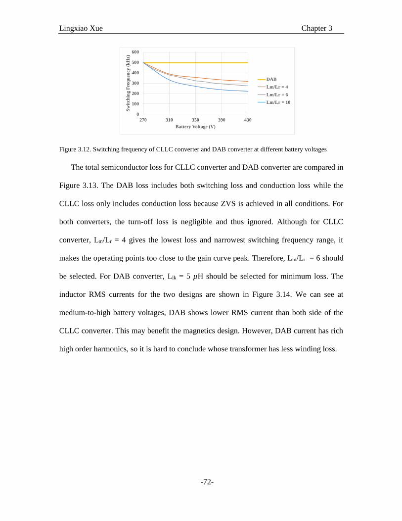
Lingxiao Xue Chapter 3
-72-
Figure 3.12. Switching frequency of CLLC converter and DAB converter at different battery voltages
The total semiconductor loss for CLLC converter and DAB converter are compared in
Figure 3.13. The DAB loss includes both switching loss and conduction loss while the
CLLC loss only includes conduction loss because ZVS is achieved in all conditions. For
both converters, the turn-off loss is negligible and thus ignored. Although for CLLC
converter, Lm/Lr = 4 gives the lowest loss and narrowest switching frequency range, it
makes the operating points too close to the gain curve peak. Therefore, Lm/Lr = 6 should
be selected. For DAB converter, Llk = 5 µH should be selected for minimum loss. The
inductor RMS currents for the two designs are shown in Figure 3.14. We can see at
medium-to-high battery voltages, DAB shows lower RMS current than both side of the
CLLC converter. This may benefit the magnetics design. However, DAB current has rich
high order harmonics, so it is hard to conclude whose transformer has less winding loss.
0
100
200
300
400
500
600
270 310 350 390 430
Sw
itch
ing F
req
uen
cy (
kH
z)Battery Voltage (V)
DAB
Lm/Lr = 4
Lm/Lr = 6
Lm/Lr = 10
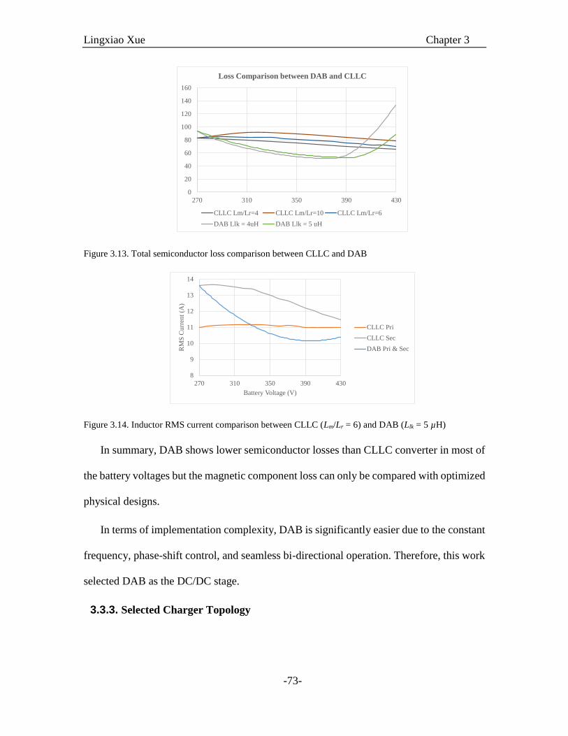
Lingxiao Xue Chapter 3
-73-
Figure 3.13. Total semiconductor loss comparison between CLLC and DAB
Figure 3.14. Inductor RMS current comparison between CLLC (Lm/Lr = 6) and DAB (Llk = 5 µH)
In summary, DAB shows lower semiconductor losses than CLLC converter in most of
the battery voltages but the magnetic component loss can only be compared with optimized
physical designs.
In terms of implementation complexity, DAB is significantly easier due to the constant
frequency, phase-shift control, and seamless bi-directional operation. Therefore, this work
selected DAB as the DC/DC stage.
3.3.3. Selected Charger Topology
0
20
40
60
80
100
120
140
160
270 310 350 390 430
Loss Comparison between DAB and CLLC
CLLC Lm/Lr=4 CLLC Lm/Lr=10 CLLC Lm/Lr=6
DAB Llk = 4uH DAB Llk = 5 uH
8
9
10
11
12
13
14
270 310 350 390 430
RM
S C
urr
ent
(A)
Battery Voltage (V)
CLLC Pri
CLLC Sec
DAB Pri & Sec
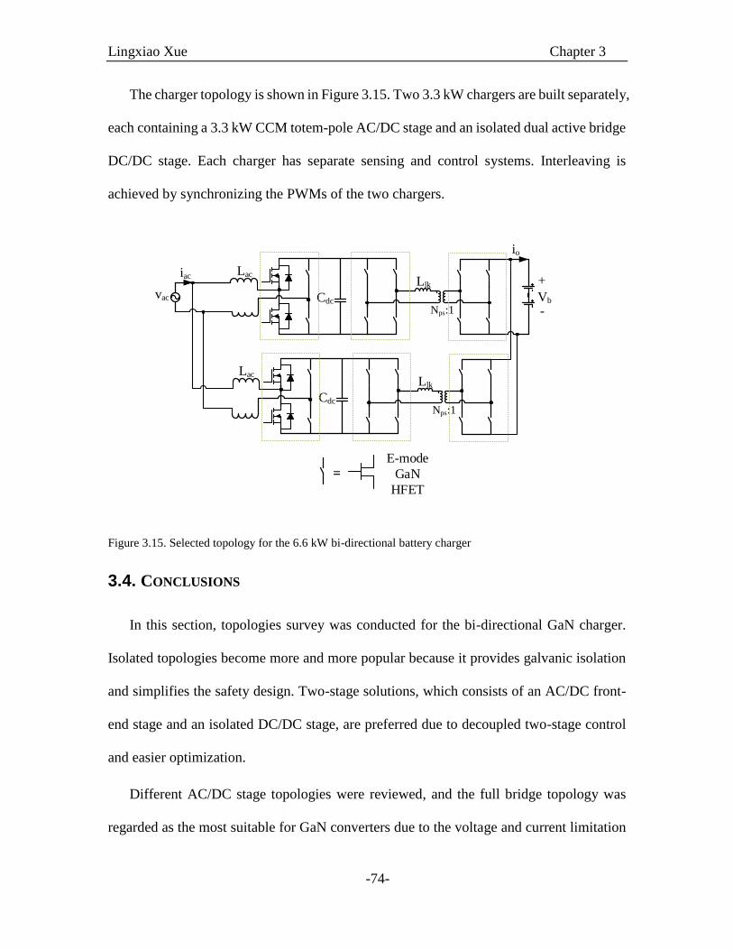
Lingxiao Xue Chapter 3
-74-
The charger topology is shown in Figure 3.15. Two 3.3 kW chargers are built separately,
each containing a 3.3 kW CCM totem-pole AC/DC stage and an isolated dual active bridge
DC/DC stage. Each charger has separate sensing and control systems. Interleaving is
achieved by synchronizing the PWMs of the two chargers.
Lac
Cdcvac
Nps:1
Llk +
-Vb
iac
io
Lac
Cdc
Nps:1
Llk
=
E-mode
GaN
HFET
Figure 3.15. Selected topology for the 6.6 kW bi-directional battery charger
3.4. CONCLUSIONS
In this section, topologies survey was conducted for the bi-directional GaN charger.
Isolated topologies become more and more popular because it provides galvanic isolation
and simplifies the safety design. Two-stage solutions, which consists of an AC/DC front-
end stage and an isolated DC/DC stage, are preferred due to decoupled two-stage control
and easier optimization.
Different AC/DC stage topologies were reviewed, and the full bridge topology was
regarded as the most suitable for GaN converters due to the voltage and current limitation
Lingxiao Xue Chapter 3
-75-
of GaN devices. Two modulation methods were compared, namely, the continuous
conduction mode and the triangular conduction mode. The TCM modulation offers lower
loss because of zero-voltage switching, but the modulation and interleaving realization are
significantly more complicated. Therefore, CCM modulation is adopted.
Bi-directional DC/DC converters were reviewed as well. Fast switching transitions of
GaN rule out those topologies that have long commutation loops and offer no voltage
clamping across the switches. Two candidate topologies, DAB and CLLC converter, were
then compared. It turned out that DAB gives lower semiconductor loss than the CLLC
converter does in most of the battery voltages. The magnetic loss comparison is not obvious
without going through detailed physical designs. As the battery charger already needs to
deal with wide voltage and current range, the DAB topology with a constant frequency is
selected for easier converter design and optimization.
3.5. LIST OF REFERENCES
[1] Z. Xiaohu, W. Gangyao, S. Lukic, S. Bhattacharya, and A. Huang, "Multi-function
bi-directional battery charger for plug-in hybrid electric vehicle application," in
Proc. IEEE Energy Convers. Congr. Expo., 2009, pp. 3930-3936.
[2] X. Zhou, "Design and Control of Bi-Directional Grid-Interactive Converter for
Plug-in Hybrid Electric Vehicle Applications," Ph.D. Dissertation, North Carolina
State University, Ann Arbor, 2011.
[3] C. Gyu-Yeong, K. Jong-Soo, L. Byoung-kuk, W. Chung-Yuen, and L. Tea-Won,
"A Bi-directional battery charger for electric vehicles using photovoltaic PCS
systems," in Proc. IEEE Veh. Power Propulsion Conf., 2010, pp. 1-6.
[4] M. C. Kisacikoglu, B. Ozpineci, and L. M. Tolbert, "Examination of a PHEV
bidirectional charger system for V2G reactive power compensation," in Proc. IEEE
Appl. Power Electron. Conf. Expo., 2010, pp. 458-465.
[5] D. Yu, Z. Xiaohu, B. Sanzhong, S. Lukic, and A. Huang, "Review of non-isolated
bi-directional DC-DC converters for plug-in hybrid electric vehicle charge station
application at municipal parking decks," in Proc. IEEE Appl. Power Electron. Conf.
Expo., 2010, pp. 1145-1151.
[6] K. Acharya, S. K. Mazumder, and P. Jedraszczak, "Efficient, High-Temperature
Bidirectional Dc/Dc Converter for Plug-in-Hybrid Electric Vehicle (PHEV) using
Lingxiao Xue Chapter 3
-76-
SiC Devices," in Proc. IEEE Appl. Power Electron. Conf. Expo., 2009, pp. 642-
648.
[7] S. Haghbin, S. Lundmark, M. Alakula, and O. Carlson, "Grid-Connected Integrated
Battery Chargers in Vehicle Applications: Review and New Solution," IEEE Trans.
Ind. Electron., vol. 60, no. 2, pp. 459-473, 2013.
[8] S. Norrga, "Experimental Study of a Soft-Switched Isolated Bidirectional
AC–DC Converter Without Auxiliary Circuit," IEEE Trans. Power
Electron., vol. 21, no. 6, pp. 1580-1587, 2006.
[9] S. N. Vaishnav and H. Krishnaswami, "Single-stage isolated bi-directional
converter topology using high frequency AC link for charging and V2G
applications of PHEV," in Proc. IEEE Veh. Power Propulsion Conf., 2011, pp. 1-
4.
[10] G. Castelino, K. Basu, N. Weise, and N. Mohan, "A bi-directional, isolated, single-
stage, DAB-based AC-DC converter with open-loop power factor correction and
other advanced features," in Proc. IEEE Int. Conf. Ind. Technol., 2012, pp. 938-
943.
[11] F. Jauch and J. Biela, "Single-phase single-stage bidirectional isolated ZVS AC-
DC converter with PFC," in Power Electronics and Motion Control Conference
Proc. Int. Power Electro. and Motion Control Conf., 2012, pp. LS5d.1-1-LS5d.1-
8.
[12] D. J. Thrimawithana, U. K. Madawala, R. Twiname, and D. M. Vilathgamuwa, "A
novel matrix converter based resonant dual active bridge for V2G applications," in
Proc. Conf. Power & Energy, 2012, pp. 503-508.
[13] N. Reimensnyder and N. Weise, "Voltage control of a single phase, single-stage,
isolated AC-DC converter," in Proc. Transportation Electrification Conf. and
Expo., 2013, pp. 1-5.
[14] N. Weise and L. Doiron, "DQ current control of a bidirectional, isolated single-
stage AC-DC converter," in Proc. IEEE Appl. Power Electron. Conf. Expo., 2014,
pp. 1888-1893.
[15] N. D. Weise, G. Castelino, K. Basu, and N. Mohan, "A Single-Stage Dual-Active-
Bridge-Based Soft Switched AC/DC Converter With Open-Loop Power Factor
Correction and Other Advanced Features," IEEE Trans. Power Electron., vol. 29,
no. 8, pp. 4007-4016, 2014.
[16] J. Everts, F. Krismer, J. Van den Keybus, J. Driesen, and J. W. Kolar, "Optimal
ZVS Modulation of Single-Phase Single-Stage Bidirectional DAB AC/DC
Converters," IEEE Trans. Power Electron., vol. 29, no. 8, pp. 3954-3970, 2014.
[17] B. Singh, B. N. Singh, A. Chandra, K. Al-Haddad, A. Pandey, and D. P. Kothari,
"A review of single-phase improved power quality AC-DC converters," IEEE
Trans. Ind. Electron., vol. 50, no. 5, pp. 962-981, 2003.
[18] J. P. M. Figueiredo, F. L. Tofoli, and B. L. A. Silva, "A review of single-phase PFC
topologies based on the boost converter," in Proc. IEEE/IAS Int. Conf. Ind. Appl.,
2010, pp. 1-6.
[19] K. Keun-Wan, K. Dong-Hee, W. Dong-Gyun, and L. Byoung-Kuk, "Topology
comparison for 6.6kW On board charger: Performance, efficiency, and selection
guideline," in Proc. IEEE Veh. Power Propulsion Conf., 2012, pp. 1520-1524.

Lingxiao Xue Chapter 3
-77-
[20] F. Musavi, M. Edington, W. Eberle, and W. G. Dunford, "Evaluation and
Efficiency Comparison of Front End AC-DC Plug-in Hybrid Charger Topologies,"
IEEE Trans. Smart Grid, vol. 3, no. 1, pp. 413-421, 2012.
[21] D. C. Erb, O. C. Onar, and A. Khaligh, "Bi-directional charging topologies for plug-
in hybrid electric vehicles," in Proc. IEEE Appl. Power Electron. Conf. Expo., 2010,
pp. 2066-2072.
[22] D. Dong, I. Cvetkovic, D. Boroyevich, W. Zhang, R. Wang, and P. Mattavelli,
"Grid-Interface Bidirectional Converter for Residential DC Distribution Systems
Part One: High-Density Two-Stage Topology," IEEE Trans. Power Electron., vol.
28, no. 4, pp. 1655-1666, 2013.
[23] D. Segaran, D. G. Holmes, and B. P. McGrath, "High-performance bi-directional
AC-DC converters for PHEV with minimised DC bus capacitance," in Proc. Ann.
Conf. IEEE Ind. Electron., 2011, pp. 3620-3625.
[24] M. C. Kisacikoglu, B. Ozpineci, and L. M. Tolbert, "Reactive power operation
analysis of a single-phase EV/PHEV bidirectional battery charger," in Proc. IEEE
Int. Conf. Power Electron., 2011, pp. 585-592.
[25] H. Kim and K.-H. Kim, "Filter design for grid connected PV inverters," in Proc.
IEEE Int. Conf. Sustainable Energy Technol., 2008, pp. 1070-1075.
[26] X. Lingxiao, S. Zhiyu, D. Boroyevich, and P. Mattavelli, "GaN-based high
frequency totem-pole bridgeless PFC design with digital implementation," in Proc.
IEEE Appl. Power Electron. Conf. Expo., 2015, pp. 759-766.
[27] R. Srinivasan and R. Oruganti, "A unity power factor converter using half-bridge
boost topology," IEEE Trans. Power Electron., vol. 13, no. 3, pp. 487-500, 1998.
[28] N. Tuan, W. Jehyuk, and N. Kwanghee, "A single-phase bidirectional dual active
half-bridge converter," in Proc. IEEE Appl. Power Electron. Conf. Expo., 2012, pp.
1127-1133.
[29] L. Bor-Ren, C. Der-Jan, and H. Tsung-Liang, "Half-bridge neutral point diode
clamped rectifier for power factor correction," IEEE Trans. Aerosp. Electron. Syst.,
vol. 38, no. 4, pp. 1287-1294, 2002.
[30] N. Wong and M. Kazerani, "A review of bidirectional on-board charger topologies
for plugin vehicles," in Proc. IEEE Can. Conf. Elect. Comput. Eng., 2012, pp. 1-6.
[31] D. Yu, S. Lukic, B. Jacobson, and A. Huang, "Review of high power isolated bi-
directional DC-DC converters for PHEV/EV DC charging infrastructure," in Proc.
IEEE Energy Convers. Congr. Expo., 2011, pp. 553-560.
[32] A. Khaligh and S. Dusmez, "Comprehensive Topological Analysis of Conductive
and Inductive Charging Solutions for Plug-In Electric Vehicles," IEEE Trans. Veh.
Technol., vol. 61, no. 8, pp. 3475-3489, 2012.
[33] F. Krismer, "Modeling and optimization of bidirectional dual active bridge DC-DC
converter topologies," Ph.D. Disstation., Eidgenössische Technische Hochschule
ETH Zürich, 2010.
[34] R. W. A. A. De Doncker, D. M. Divan, and M. H. Kheraluwala, "A three-phase
soft-switched high-power-density DC/DC converter for high-power applications,"
IEEE Trans. Ind. Appl., vol. 27, no. 1, pp. 63-73, 1991.
[35] G. G. Oggier, G. O. Garcia, and A. R. Oliva, "Switching Control Strategy to
Minimize Dual Active Bridge Converter Losses," IEEE Trans. Power Electron.,
vol. 24, no. 7, pp. 1826-1838, 2009.
Lingxiao Xue Chapter 3
-78-
[36] S. Zhiyu, R. Burgos, D. Boroyevich, and F. Wang, "Soft-switching capability
analysis of a dual active bridge dc-dc converter," in Proc. IEEE Elect. Ship Technol.
Symp., 2009, pp. 334-339.
[37] F. Krismer, J. Biela, and J. W. Kolar, "A comparative evaluation of isolated bi-
directional DC/DC converters with wide input and output voltage range," in Proc.
Ind. Appl. Conf., 2005, pp. 599-606 Vol. 1.
[38] A. Hillers, D. Christen, and J. Biela, "Design of a Highly efficient bidirectional
isolated LLC resonant converter," in Proc. Int. Power Electro. and Motion Control
Conf.,, 2012, pp. DS2b.13-1-DS2b.13-8.
[39] J. Jee-Hoon, K. Ho-Sung, K. Jong-Hyun, R. Myoung-Hyo, and B. Ju-Won, "High
efficiency bidirectional LLC resonant converter for 380V DC power distribution
system using digital control scheme," in Proc. IEEE Appl. Power Electron. Conf.
Expo., 2012, pp. 532-538.
[40] J. H. Jung, H. S. Kim, M. H. Ryu, and J. W. Baek, "Design Methodology of
Bidirectional CLLC Resonant Converter for High-Frequency Isolation of DC
Distribution Systems," IEEE Trans. Power Electron., vol. 28, no. 4, pp. 1741-1755,
2013.
[41] K. Eun-Soo, P. Jun-Hyoung, J. Jong-Sung, L. Seung-Min, K. Kwangseob, and K.
Young-Su, "Bidirectional DC-DC converter using secondary LLC resonant tank,"
in Proc. IEEE Appl. Power Electron. Conf. Expo., 2015, pp. 2104-2108.
[42] T. Jiang, j. zhang, x. wu, K. Sheng, and Y. Wang, "A Bidirectional Three-level LLC
Resonant Converter with PWAM Control," IEEE Trans. Power Electron., vol. PP,
no. 99, pp. 1-1, 2015.
[43] J. Tianyang, Z. Junming, W. Xinke, S. Kuang, and W. Yousheng, "A Bidirectional
LLC Resonant Converter With Automatic Forward and Backward Mode
Transition," IEEE Trans. Power Electron., vol. 30, no. 2, pp. 757-770, 2015.
[44] H.-J. Chae, H.-T. Moon, and J.-Y. Lee, "On-board battery charger for PHEV
without high-voltage electrolytic capacitor," Electron. Lett., vol. 46, no. 25, pp.
1691-1692, 2010.
[45] L. Jih-Sheng and D. Chen, "Design consideration for power factor correction boost
converter operating at the boundary of continuous conduction mode and
discontinuous conduction mode," in A Proc. IEEE Appl. Power Electron. Conf.
Expo., 1993, pp. 267-273.
[46] C. Marxgut, J. Biela, and J. W. Kolar, "Interleaved Triangular Current Mode (TCM)
resonant transition, single phase PFC rectifier with high efficiency and high power
density," in Proc. Int. Power Electron. Conf., 2010, pp. 1725-1732.
[47] L. Zhengyang, H. Xiucheng, M. Mingkai, Y. Yuchen, F. C. Lee, and L. Qiang,
"Design and evaluation of GaN-based dual-phase interleaved MHz critical mode
PFC converter," in Proc. IEEE Energy Convers. Congr. Expo., 2014, pp. 611-616.
[48] "Gallium-Nitride Switch Technology for Bi-directional Battery-to-Grid Charger
Applications," Arpa-E ADEPT Project Report. Awards number: DE-AR-0000117,
2014.
[49] X. Lingxiao, M. Mingkai, D. Boroyevich, and P. Mattavelli, "The optimal design
of GaN-based Dual Active Bridge for bi-directional Plug-IN Hybrid Electric
Vehicle (PHEV) charger," in Proc. IEEE Appl. Power Electron. Conf. Expo., 2015,
pp. 602-608.

Lingxiao Xue Chapter 4
-79-
Chapter 4. CHARGING WAVEFORM OPTIMIZATION TO REDUCE DC
LINK CAPACITANCE
4.1. SINUSOIDAL CHARGING CONCEPT AND REALIZATION
4.1.1. Introduction
Equation Chapter (Next) Section 1As discussed in Chapter 1, the on-board Level 2
battery charger topology usually adopts a single-phase AC-to-DC converter that interfaces
with a household electrical outlet [1]. As Power Factor Correction (PFC) is required, the
AC input voltage and current will be sinusoidal so that input power pulsates at two times
the line frequency. This pulsating power is usually stored in a capacitor bank, which has
high capacitance, high volume, and low lifetime if electrolytic capacitors are used. The
size of the DC link capacitor is determined by the ripple power at two times the line
frequency instead of the switching ripple; therefore, the DC link capacitors become the
major power density barrier of the battery charger when wide band gap devices are used
[2].
Researchers have made large efforts to reduce the DC link capacitance in order to avoid
using an electrolytic capacitor for a longer lifetime, while meanwhile keeping a high power
density in different single-phase AC-DC energy conversion applications. In LED driver
applications, the overall ripple energy at double line frequency can be reduced by
moderately distorting the AC input current, while the resultant power factor can still fulfill
the standard requirement [3, 4]. Inductive storage can be used to replace the low-lifetime
capacitors [5, 6], but this will also reduce the overall power density due to its lower energy

Lingxiao Xue Chapter 4
-80-
density as compared to capacitive storage (i.e. capacitors) [7]. Given the same ripple
energy, the capacitance is reduced by enlarging the capacitor voltage ripple. This concept
can be implemented directly to the DC link capacitor, as shown in a grid-interface bi-
directional converter [8], which increases device voltage stress. Alternatively, it can be
implemented in the auxiliary capacitors [7, 9-11], with increased realization complexity.
Specifically for battery chargers, if the battery pack can take the low frequency
charging current ripple, the DC link capacitance will be significantly reduced because the
capacitors only need to filter the current ripple at the switching frequency. Reference [12]
and [13] compare battery capacity under DC charging and pulse charging with similar
current waveforms, which this paper will employs, and the difference is minor: 0.55% and
-1.4%, respectively. Reference [14] shows an approximate 2 oC temperature rise due to
increased RMS value. In all, although long-term tests on battery lifetime are certainly
necessary, short term results show that two times line frequency ripple current causes minor
impact to battery capacity and temperature rise.
Therefore, it is possible to propose charger designs with the charging current
containing low-frequency ripples. This concept can be employed in various charger
topologies and realized by different control schemes. Most single-stage topologies only
have energy storage at the output; therefore, the times two line frequency ripple will
naturally flow into the battery [15-17]. Multiple-stage designs in [18-21] directly feed the
rectified AC voltage to the DC/DC stages to realize both galvanic isolation and charging
power conditioning; therefore, no regulated DC link is present. In [22], the DC link voltage
is closed-loop controlled to have designated DC and ripple amplitude, but the steady state
error of the ripple exists due to insufficient gain of PI controller at the ripple frequency.
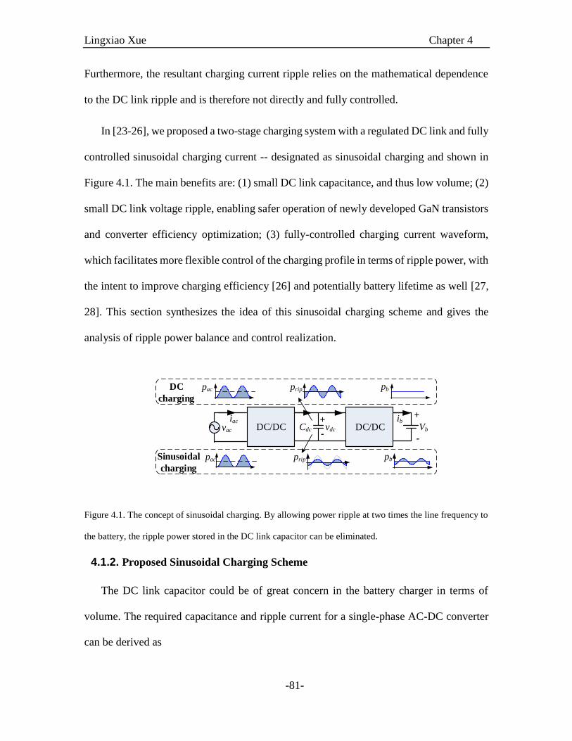
Lingxiao Xue Chapter 4
-81-
Furthermore, the resultant charging current ripple relies on the mathematical dependence
to the DC link ripple and is therefore not directly and fully controlled.
In [23-26], we proposed a two-stage charging system with a regulated DC link and fully
controlled sinusoidal charging current -- designated as sinusoidal charging and shown in
Figure 4.1. The main benefits are: (1) small DC link capacitance, and thus low volume; (2)
small DC link voltage ripple, enabling safer operation of newly developed GaN transistors
and converter efficiency optimization; (3) fully-controlled charging current waveform,
which facilitates more flexible control of the charging profile in terms of ripple power, with
the intent to improve charging efficiency [26] and potentially battery lifetime as well [27,
28]. This section synthesizes the idea of this sinusoidal charging scheme and gives the
analysis of ripple power balance and control realization.
DC/DCDC/DC
DC
charging
Sinusoidal
charging
pac prip pb
pac prip pb
vac
iac
Cdc vdc
ibVb
-
+
-
+
Figure 4.1. The concept of sinusoidal charging. By allowing power ripple at two times the line frequency to
the battery, the ripple power stored in the DC link capacitor can be eliminated.
4.1.2. Proposed Sinusoidal Charging Scheme
The DC link capacitor could be of great concern in the battery charger in terms of
volume. The required capacitance and ripple current for a single-phase AC-DC converter
can be derived as
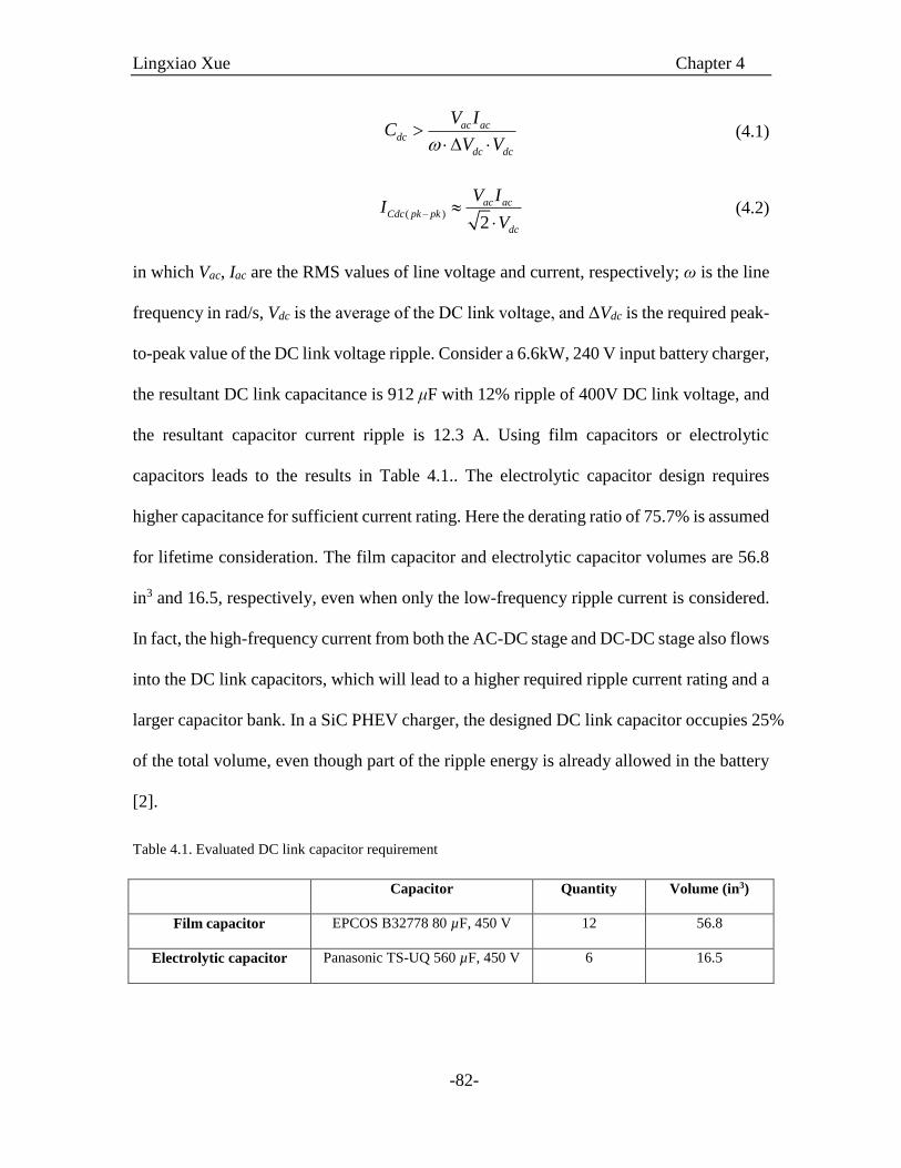
Lingxiao Xue Chapter 4
-82-
ac ac
dc
dc dc
V IC
V V
(4.1)
( )2
ac acCdc pk pk
dc
V II
V
(4.2)
in which Vac, Iac are the RMS values of line voltage and current, respectively; ω is the line
frequency in rad/s, Vdc is the average of the DC link voltage, and ΔVdc is the required peak-
to-peak value of the DC link voltage ripple. Consider a 6.6kW, 240 V input battery charger,
the resultant DC link capacitance is 912 μF with 12% ripple of 400V DC link voltage, and
the resultant capacitor current ripple is 12.3 A. Using film capacitors or electrolytic
capacitors leads to the results in Table 4.1.. The electrolytic capacitor design requires
higher capacitance for sufficient current rating. Here the derating ratio of 75.7% is assumed
for lifetime consideration. The film capacitor and electrolytic capacitor volumes are 56.8
in3 and 16.5, respectively, even when only the low-frequency ripple current is considered.
In fact, the high-frequency current from both the AC-DC stage and DC-DC stage also flows
into the DC link capacitors, which will lead to a higher required ripple current rating and a
larger capacitor bank. In a SiC PHEV charger, the designed DC link capacitor occupies 25%
of the total volume, even though part of the ripple energy is already allowed in the battery
[2].
Table 4.1. Evaluated DC link capacitor requirement
Capacitor Quantity Volume (in3)
Film capacitor EPCOS B32778 80 µF, 450 V 12 56.8
Electrolytic capacitor Panasonic TS-UQ 560 µF, 450 V 6 16.5

Lingxiao Xue Chapter 4
-83-
If all ripple power flows into the batteries, also taking into account a constant battery
voltage in the double line frequency period, the charging current in a lossless condition will
have a sinusoidal waveform with a DC bias as
( ) 2 sin( ) 2 sin( ) / (1 cos2 )b ac ac b bi t V t I t V I t (4.3)
where Ib is the average charging current, which comes from the required charging profile.
The ripple power at two times the line frequency in (4.3) is equal to the ripple power at the
input side. Thus, no ripple power need to be stored in the charger, and the DC link
capacitors can be eliminated. In this paper, charging with current in the form of (4.3) is
called as sinusoidal (current) charging. Note that the amplitude of the current ripple in (4.3)
equals the DC component.
The battery charger under investigation contains one full bridge (FB) AC-DC stage and
one dual active bridge (DAB) DC-DC stage, as shown in Figure 4.2. In this configuration,
the FB AC-DC stage is controlled to realize power factor correction and DC link voltage
regulation, and the DAB DC-DC stage is used to achieve sinusoidal charging. Since
charging current waveform mainly influences the DC-DC stage, the next section will focus
on the analysis and control design of the DAB DC-DC stage with sinusoidal charging.
LacCdc
+
-
vdcvac
Nps:1
Llk+
-
Vb
iac ib
+-
vp +-
vsilk Co
Figure 4.2. Battery charger topology with a Full Bridge (FB) AC-DC stage plus a Dual Active Bridge (DAB)
DC-DC stage
4.1.3. Dual Active Bridge Operation with Sinusoidal Charging Current
Lingxiao Xue Chapter 4
-84-
In this work, phase shift modulation (PSM) of DAB is used to demonstrate the concept
of sinusoidal charging for simplicity. With phase shift modulation, each device is driven
with a 50% duty cycle and the two-phase legs at the same side have a 180-degree phase
shift, so that both of the full bridge output voltages (vp and vs) are 50% of the duty cycle
square wave. These two output square waves have, and have only, Vdc and – Vdc values,
which show the characteristics of two level modulations. When applied to a phase shift by
an angle φ to these two square waves, the average output current can be derived as [29]
2
( )( )
2
ps dc
o
s lk
N Vi
f L
(4.4)
in which Nps is the transformer and turns ratio from the primary to secondary sides, Vdc is
the DC link voltage, φ is the phase shift angle, fs is the switching frequency, Vb is the battery
voltage, and Llk is the leakage inductance of the DAB transformer. We can see that the
DAB with a phase shift modulation is a current source in nature. Considering (4.3) and
(4.4), the steady state value of phase shift within the line period can be solved as
8 (1 cos 2 )
( ) (1 1 )2
s lk b
ps dc
f L I tt
N V
(4.5)
The phase shift shown in (4.5) is the steady state phase shift when sinusoidal charging is
achieved.
Soft-switching is important to reduce switching loss, especially for a converter with
both high switching frequency and high power density. For the power MOSFET, zero
voltage switching (ZVS) is usually preferable. ZVS always means the device turning on
transition is initiated by the conduction of a body diode or anti-parallel diode. In the ideal
case, the influence of a device output capacitor and transformer magnetizing inductance

Lingxiao Xue Chapter 4
-85-
are ignored. Hence, ZVS condition is only determined by the current direction before the
switch is turned on. Therefore, the inductor current at the device transition instants t0 and
t1, as shown in Figure 4.3, should satisfy the following inequalities to achieve ZVS for
primary bridge and secondary bridge, respectively.
0( ) 0pi t (4.6)
1( ) 0pi t (4.7)
when (4.6) and (4.7) are satisfied, the other half-cycle of the ZVS conditions automatically
hold because of the half-cycle symmetry of the inductor current waveform.
π
ip
t
vp
vs
φ1 φ2
π
ip
t
vp
vs
φ2 φ1
(a) (b)
t1t0 t0 t1
Figure 4.3. DAB waveforms with phase-shift modulation at different phase shift values. (a) Vdc>NpsVb, (b)
Vdc<NpsVb
Making the two current items in (4.6) and (4.7) equal to zero yields the PSM DAB ZVS
boundary, which divides the entire operating range into three regions, as shown in Figure
4.4. The ZVS boundary is usually plotted on a normalized voltage/current map [29]. The
horizontal axis is the normalized voltage, which is defined as
/nom ps b dcV N V V (4.8)
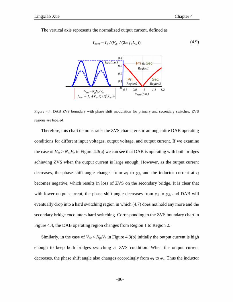
Lingxiao Xue Chapter 4
-86-
The vertical axis represents the normalized output current, defined as
/ ( / (2 ))nom o sdc lkI I V f L (4.9)
Figure 4.4. DAB ZVS boundary with phase shift modulation for primary and secondary switches; ZVS
regions are labeled
Therefore, this chart demonstrates the ZVS characteristic among entire DAB operating
conditions for different input voltages, output voltage, and output current. If we examine
the case of Vdc > NpsVb in Figure 4.3(a) we can see that DAB is operating with both bridges
achieving ZVS when the output current is large enough. However, as the output current
decreases, the phase shift angle changes from φ1 to φ2, and the inductor current at t1
becomes negative, which results in loss of ZVS on the secondary bridge. It is clear that
with lower output current, the phase shift angle decreases from φ1 to φ2, and DAB will
eventually drop into a hard switching region in which (4.7) does not hold any more and the
secondary bridge encounters hard switching. Corresponding to the ZVS boundary chart in
Figure 4.4, the DAB operating region changes from Region 1 to Region 2.
Similarly, in the case of Vdc < NpsVb in Figure 4.3(b) initially the output current is high
enough to keep both bridges switching at ZVS condition. When the output current
decreases, the phase shift angle also changes accordingly from φ1 to φ2. Thus the inductor
Vnom (p.u.)
Inom (p.u.)
0.8 0.9 1 1.10
0.1
0.2
0.3
0.4
1.2
Region 1
Region 2 Region 3
))2/(/( lksdconom LfVII dcbpsnom VVNV /
Pri & Sec
Pri Sec

Lingxiao Xue Chapter 4
-87-
current at t0 becomes positive which violates (4.6), leading to hard switching on the
primary bridge. In this case, the operating region changes from Region 1 to Region 3.
From the above analysis, we can see that if sinusoidal charging is adopted, hard
switching of the devices always occurs, due to the severe variation of the sinusoidal output
current. In fact, the DAB switching condition with under sinusoidal charging is more
complicated when the switch parasitic capacitances and the deadtime are considered. This
will be detailed in Section 5.3.2.
4.1.4. Control Design and Implementation of Sinusoidal Charging on a Dual Active
Bridge Converter
In this section, we will focus on the influence of the sinusoidal charging in the control
of the output current of the DAB. The target of the control strategy is to obtain the
regulation of DAB output current in the form of (4.3). In state-of-art implementations, a
low bandwidth PI controller is usually used to control the DC charging current of the
battery [30-32] and in [33], a 20 Hz current regulator is used. The main advantages of this
implementation are good performance and simplicity. However, for this particular
application, the sinusoidal charging of the batteries requires a control strategy with a
bandwidth as high as possible in order to obtain a high instantaneous power balance
between the mains and the batteries, as explained in Section 4.1.2. A digital control has
been chosen to control the two-stage (PFC and DAB) converter due to its high flexibility
and reliability, the possibility to synchronize the control of both stages, and the ease of
monitoring the control and converter parameters. The block diagram of the DAB’s control
scheme can be seen in Figure 4.5. The phase shift to output current transfer function Giφ
can be obtained as (4.10) by perturbation and linearization on (4.4)
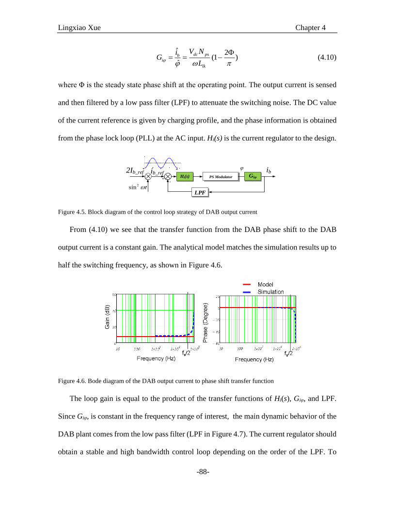
Lingxiao Xue Chapter 4
-88-
ˆ 2
(1 )ˆ
dc psbi
lk
V NiG
L
(4.10)
where Φ is the steady state phase shift at the operating point. The output current is sensed
and then filtered by a low pass filter (LPF) to attenuate the switching noise. The DC value
of the current reference is given by charging profile, and the phase information is obtained
from the phase lock loop (PLL) at the AC input. Hi(s) is the current regulator to the design.
LPF
+-
2Ib_refPS ModulatorHi(s)
ibGiφ
φ ib_ref
Figure 4.5. Block diagram of the control loop strategy of DAB output current
From (4.10) we see that the transfer function from the DAB phase shift to the DAB
output current is a constant gain. The analytical model matches the simulation results up to
half the switching frequency, as shown in Figure 4.6.
Figure 4.6. Bode diagram of the DAB output current to phase shift transfer function
The loop gain is equal to the product of the transfer functions of Hi(s), Giφ, and LPF.
Since Giφ, is constant in the frequency range of interest, the main dynamic behavior of the
DAB plant comes from the low pass filter (LPF in Figure 4.7). The current regulator should
obtain a stable and high bandwidth control loop depending on the order of the LPF. To

Lingxiao Xue Chapter 4
-89-
avoid interferences in the sinusoidal current of twice the line frequency of 120 Hz, 1.2 kHz
is also considered as the minimum cutoff frequency of the filter. With a first order filter, a
PI regulator to can achieve 20 dB/dec attentuation for the loop gain, as shown in Figure
4.7.
Magnitude
Phase
RC - LPF
PI Regulator
Filter cutoff frequency
-20dB/dec
Loop Gain
Figure 4.7. PI regulator design with a first order RC filter
4.1.5. Experimental Results
The closed-loop control strategy in section 4.1.4 is applied to a DAB converter with
the input voltage at 100V and output voltage at 90V. The DAB inductor is 53.4 µH, and
the transformer turns ratio is 40:36. A first order filter and a PI controller have been chosen
for the experimental validation of the closed loop operation as a compromise between a
high bandwidth and low computation time. Experimental waveforms for DC output current
steps are shown in Figure 4.8 for Vdc = 100 V and Vb = 90 V.
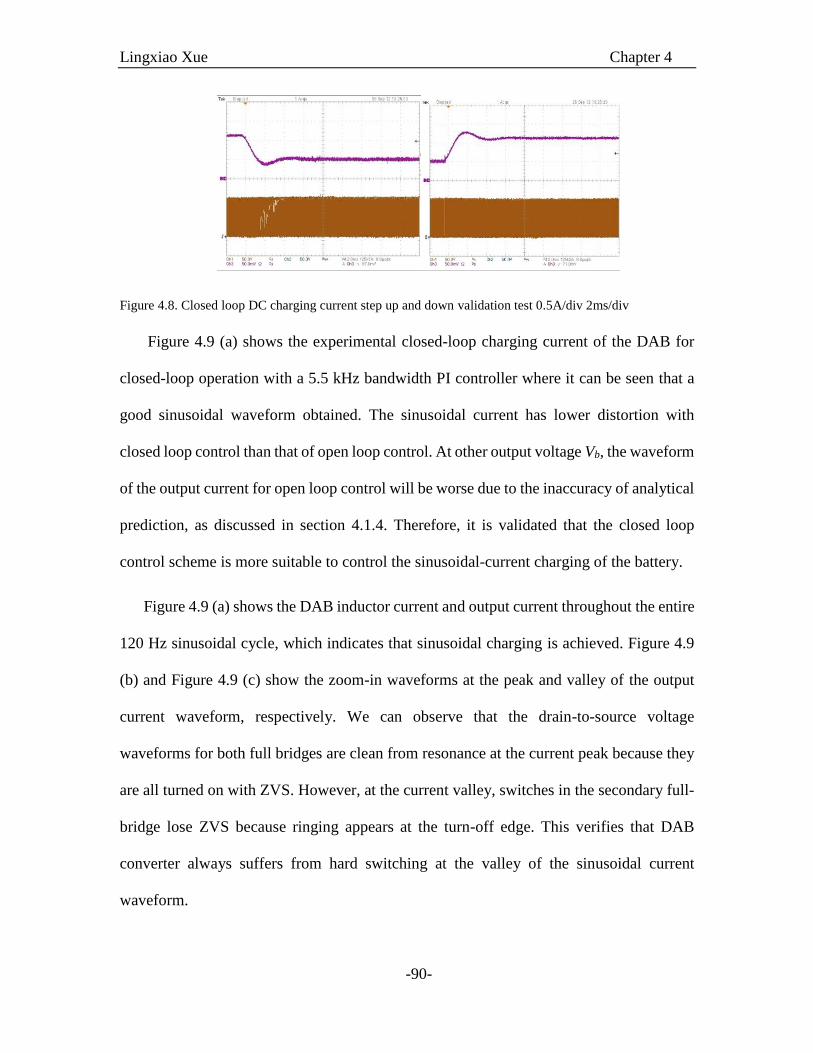
Lingxiao Xue Chapter 4
-90-
Figure 4.8. Closed loop DC charging current step up and down validation test 0.5A/div 2ms/div
Figure 4.9 (a) shows the experimental closed-loop charging current of the DAB for
closed-loop operation with a 5.5 kHz bandwidth PI controller where it can be seen that a
good sinusoidal waveform obtained. The sinusoidal current has lower distortion with
closed loop control than that of open loop control. At other output voltage Vb, the waveform
of the output current for open loop control will be worse due to the inaccuracy of analytical
prediction, as discussed in section 4.1.4. Therefore, it is validated that the closed loop
control scheme is more suitable to control the sinusoidal-current charging of the battery.
Figure 4.9 (a) shows the DAB inductor current and output current throughout the entire
120 Hz sinusoidal cycle, which indicates that sinusoidal charging is achieved. Figure 4.9
(b) and Figure 4.9 (c) show the zoom-in waveforms at the peak and valley of the output
current waveform, respectively. We can observe that the drain-to-source voltage
waveforms for both full bridges are clean from resonance at the current peak because they
are all turned on with ZVS. However, at the current valley, switches in the secondary full-
bridge lose ZVS because ringing appears at the turn-off edge. This verifies that DAB
converter always suffers from hard switching at the valley of the sinusoidal current
waveform.
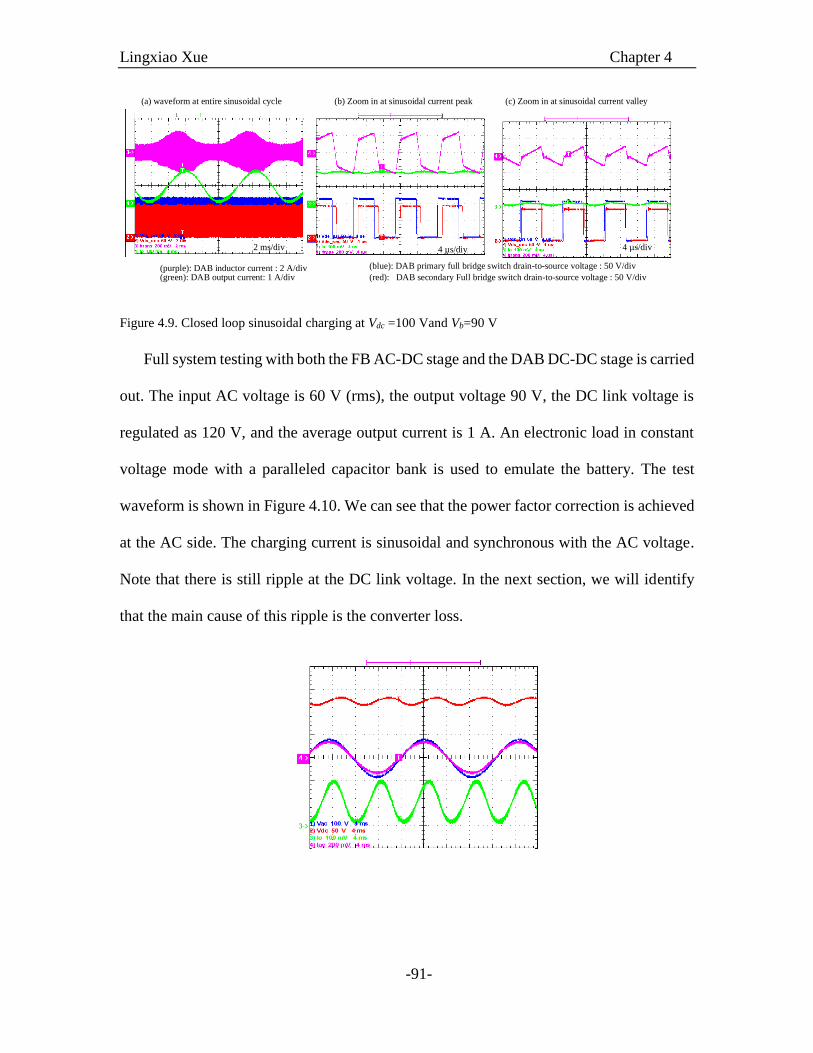
Lingxiao Xue Chapter 4
-91-
(red): DAB secondary Full bridge switch drain-to-source voltage : 50 V/div
(a) waveform at entire sinusoidal cycle (b) Zoom in at sinusoidal current peak (c) Zoom in at sinusoidal current valley
(blue): DAB primary full bridge switch drain-to-source voltage : 50 V/div
4 µs/div 4 µs/div2 ms/div
(purple): DAB inductor current : 2 A/div(green): DAB output current: 1 A/div
Figure 4.9. Closed loop sinusoidal charging at Vdc =100 Vand Vb=90 V
Full system testing with both the FB AC-DC stage and the DAB DC-DC stage is carried
out. The input AC voltage is 60 V (rms), the output voltage 90 V, the DC link voltage is
regulated as 120 V, and the average output current is 1 A. An electronic load in constant
voltage mode with a paralleled capacitor bank is used to emulate the battery. The test
waveform is shown in Figure 4.10. We can see that the power factor correction is achieved
at the AC side. The charging current is sinusoidal and synchronous with the AC voltage.
Note that there is still ripple at the DC link voltage. In the next section, we will identify
that the main cause of this ripple is the converter loss.
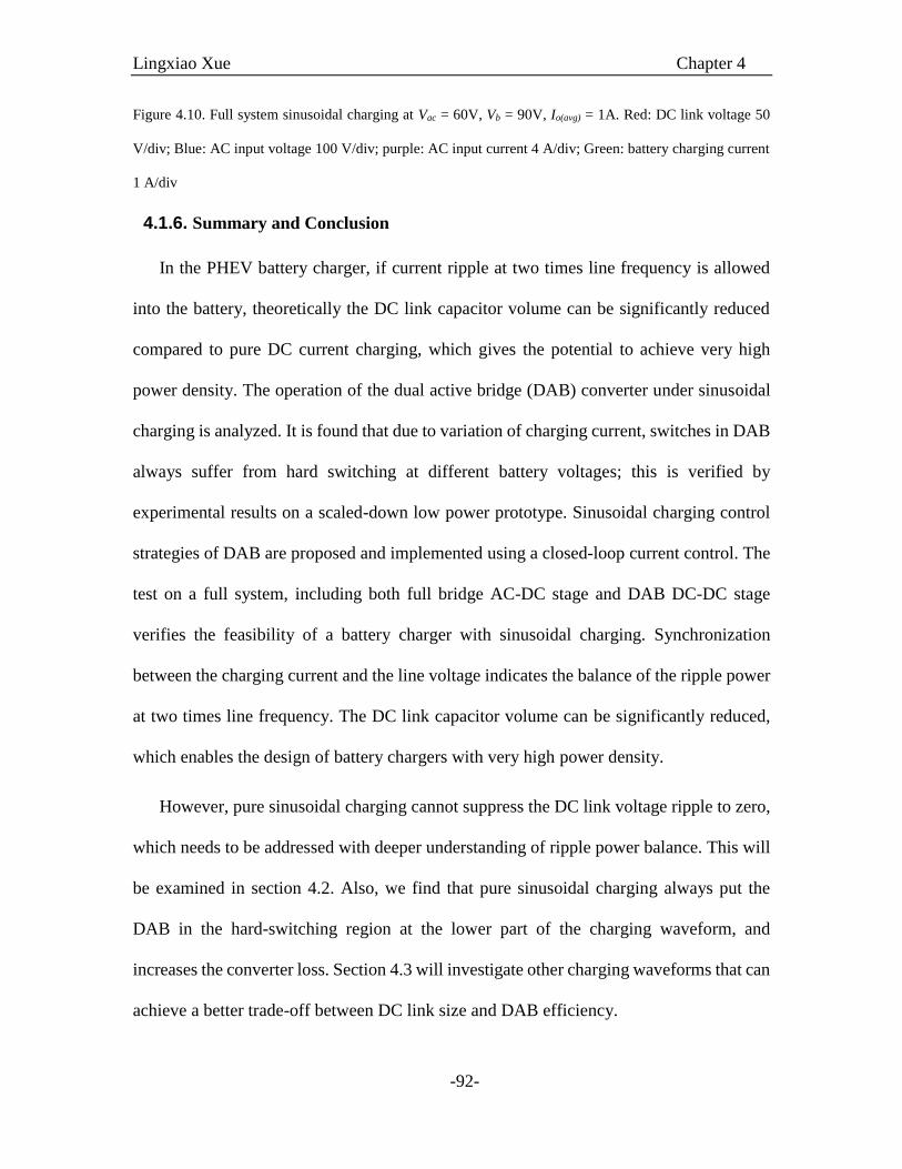
Lingxiao Xue Chapter 4
-92-
Figure 4.10. Full system sinusoidal charging at Vac = 60V, Vb = 90V, Io(avg) = 1A. Red: DC link voltage 50
V/div; Blue: AC input voltage 100 V/div; purple: AC input current 4 A/div; Green: battery charging current
1 A/div
4.1.6. Summary and Conclusion
In the PHEV battery charger, if current ripple at two times line frequency is allowed
into the battery, theoretically the DC link capacitor volume can be significantly reduced
compared to pure DC current charging, which gives the potential to achieve very high
power density. The operation of the dual active bridge (DAB) converter under sinusoidal
charging is analyzed. It is found that due to variation of charging current, switches in DAB
always suffer from hard switching at different battery voltages; this is verified by
experimental results on a scaled-down low power prototype. Sinusoidal charging control
strategies of DAB are proposed and implemented using a closed-loop current control. The
test on a full system, including both full bridge AC-DC stage and DAB DC-DC stage
verifies the feasibility of a battery charger with sinusoidal charging. Synchronization
between the charging current and the line voltage indicates the balance of the ripple power
at two times line frequency. The DC link capacitor volume can be significantly reduced,
which enables the design of battery chargers with very high power density.
However, pure sinusoidal charging cannot suppress the DC link voltage ripple to zero,
which needs to be addressed with deeper understanding of ripple power balance. This will
be examined in section 4.2. Also, we find that pure sinusoidal charging always put the
DAB in the hard-switching region at the lower part of the charging waveform, and
increases the converter loss. Section 4.3 will investigate other charging waveforms that can
achieve a better trade-off between DC link size and DAB efficiency.

Lingxiao Xue Chapter 4
-93-
4.2. SINUSOIDAL CHARGING WITH DIRECT DC LINK CONTROL
4.2.1. Introduction
In previous section, we find pure sinusoidal charging cannot balance the ripple power
at two times the line frequency, and the DC link voltage thus shows corresponding voltage
ripples. Increased DC link capacitance is required to suppress this voltage ripple.
This section will analyze the converter loss impact on the rise of DC link voltage ripple
under ideal sinusoidal charging. This DC link voltage ripple can be suppressed by a direct
control path on the voltage ripple. Compared to the scheme of the PI controller in [22], this
work examines both resonant-controller-based and synchronous-frame-based control
solutions that have a much higher control gain.
4.2.2. Converter Loss Model
In this section, the converter loss model is derived to serve as the base of ripple balance
analysis in the next section, but not for precise converter efficiency prediction. Dominant
converter losses come from semiconductor switches and magnetic components (inductor
and transformer), so other losses such as driving loss and capacitor loss are ignored.
Furthermore, to account for the power loss influence on the DC link voltage ripple at two
times the line frequency, the loss model will keep the 120 Hz component information.
4.2.2.1. AC-DC Stage Semiconductor Losses
The conduction losses pcon_PFC can be obtained given that the AC-DC stage is in
continuous conduction mode (CCM). Thus:
2
( )2
_ ( )
( )( ) ( ( ) ) 2
12
ac pp
con PFC ac ds on
i tp t i t R
(4.11)
Lingxiao Xue Chapter 4
-94-
where iac (t) is the average inductor current over the switching period, and ( ) ( )ac ppi t is the
peak-to-peak value of the inductor current ripple. If unipolar modulation is used [34],
during each switching period, two of the four switches will be switched on and off under
hard switching conditions. The other two switches will be under soft-switching, but subject
to the reverse recovery loss of their body diodes. For the hard-switching devices, the turn-
on transition is at the inductor current valley and the turn-off transition is at the inductor
current peak. Therefore, the switching loss psw_PFC _sw PFCp in the AC-DC is given by
( )
_
( )
( )
( )( ) 2 ( ( ) , )
2
( )2 ( ( ) , )
2
( )2 ( ( ) , )
2
ac pp
sw PFC on ac dc s
ac pp
off ac dc s
ac pp
rr ac dc dc s
i tp t E i t V f
i tE i t V f
i tQ i t V V f
(4.12)
where Eon and Eoff are the turn-on and turn-off energy of the selected semiconductor devices;
Vdc is the DC link voltage; fs is the switching frequency; and Qrr is the reverse recovery
charge of the body diode. The reverse recovery loss expression is detailed in [35].
4.2.2.2. AC-DC Stage Inductor Losses
The inductor loss can be divided into conduction loss and core loss. The AC side
inductor loss includes winding loss and core loss. The winding loss pcu_Lac is obtained by
2
( )2
_ _
( )( ) ( ( ) )
12
ac pp
cu Lac ac cu Lac
i tp t i t R
(4.13)
where Rcu_Lac is the resistance of the inductor winding. The inductor core loss pcore_Lac is
estimated using the Steinmetz equation as

Lingxiao Xue Chapter 4
-95-
( )
_
( )( ) ( )
2
ac ac ppx y
core Lac c s e
Lac e
L i tp t K f V
N A
(4.14)
where Kc, x, and y are the coefficients of the selected magnetic material; Lac is the boost
inductance of the AC-DC stage; Ae and Ve are the effective cross section area and the
volume of the selected magnetic core; and NLac is the number of turns of the inductor.
4.2.2.3. DC-DC Stage Semiconductor Losses
The RMS value of the leakage inductor current, while keeping the line frequency
component, can be derived as [36]
2 3 2 3
( )
1 12 ( ) 8 ( )( )
22 3
dclk rms
s lk
r r t r t Vi t
f L
(4.15)
where
dc
ps b
Vr
N V (4.16)
and the phase shift (t) is from (4.5). Since all the devices under phase-shift modulation
operate with 50% of the duty cycle and there are always two devices conducting for each
full-bridge, at any instant, the current through the leakage inductor current goes through
two devices in the primary side and two devices in the secondary side. Then the total
conduction losses in the DAB are given by
2
(_ ( )2
)( ) 2( ) (1 )c pslkon DAB ds orms n
p t i Rt N (4.17)
At r = 1 in (4.16), the DAB can achieve a maximum ZVS range with respect to the
output current level [23]. At very low switching current, partial ZVS is realized, resulting
in a switching loss that is higher compared to full ZVS but that is still negligible compared

Lingxiao Xue Chapter 4
-96-
to other losses. When r ≠ 1, the derivation of switching loss requires ZVS range judgment,
and the resultant analytical expression becomes too complicated. In section 0, we will
show the qualitative analysis of this case.
4.2.2.4. DC-DC Stage Transformer Losses
The transformer losses are comprised of winding and core losses. The winding loss
calculation is similar to that of the DAB semiconductor conduction loss. The result is
2
_tra ( )ns
2( ) N( ) ( )lk rmscu tp ps tsp t i Rt R (4.18)
where Rtp and Rts are the transformer winding resistance from the primary and secondary
sides, respectively. The core loss is estimated using the Steinmetz equation because the
flux swing does not change during the sinusoidal charging cycle. It can be determined by
_tran ( )4
x ybcore c s e
s e s
VP K f V
N A f (4.19)
where Kc, x, and y are the coefficients of the selected magnetic material; Ae and Ve are the
effective cross section area and the volume of the selected magnetic core; and Ns is the
number of turns of the secondary winding.
4.2.3. Loss Influence on Ripple Power and Ripple Power Compensation
4.2.3.1. Loss Influence on the Ripple Power of the DC Link Capacitor
Some assumptions can be made to simplify the loss model for clean and clear analytical
expressions. Firstly, the high-frequency effects are ignored due to low current ripple under
continuous conduction mode, so all the conduction losses and inductor core losses are only
considered up to 120 Hz. Secondly, both the switching energy and the reverse recovery
charge are assumed to be linear with respect to the switching current, as illustrated in [25]

Lingxiao Xue Chapter 4
-97-
for GaN devices and [35] for Si MOSFETs. Therefore, the total switching loss contains a
constant term plus a linear changing term with respect to AC current. The loss of the PFC
stage is then derived as
_ _ _
2 2
( ) _
(t) 2 sin( t)
( cos(2 t)) (2 )
loss PFC sw ac sw PFC const
ac ac ds on cu Lac
p V I P
I I R R
(4.20)
in which Psw_PFC_const is the constant term of the switching loss, and Vsw (in Volt) is the slew
rate of the linear term. The first two terms in (4.20) represent the total switching loss of the
PFC stage. The third term is the instantaneous conduction loss. Representing the resistive
terms in (4.20) via a lumped resistor RPFC and expanding (4.20) using a Fourier series
yields
2
_ _ _
2
2 2(t) ( )
4 2 4 2( )cos(2 ) cos(4 )
3 15
loss PFC sw ac ac PFC sw PFC const
sw ac ac PFC sw ac
p V I I R P
V I I R t V I t
(4.21)
Furthermore, the total losses, by neglecting the switching loss in DAB, can be described
as
2
( )_DAB _tran(t )( )loss DABlk r o ems c rp i R Pt (4.22)
where RDAB is a lumped resistor synthesizing all the different resistors in the conduction
path of ilk in (4.17) and (4.18). Assuming r = 1, Fourier series expansion on (4.22) yields
_DAB _
2
2
2
tran0.121 ( )2
0.168 ( )2
(
(t)
cos(2 )
0.05 cos(4 ))2
loss DAB core
DA
dc
s lk
dc
s lk
d
B
D Bc
s lk
A
V
f L
V
f L
V
f L
p R P
R t
R t
(4.23)

Lingxiao Xue Chapter 4
-98-
Both (4.21) and (4.23) have dominant components at DC and two times the line
frequency. Higher even-order frequencies are low in magnitude. Then the total converter
loss can be expressed as
0 2(t) cos(2 )lossp P P t (4.24)
where
2
2
2
0 _ _
_tran
2
2
2
2
0.121(2 )
0.168(
4
3 2
2 2
2
)
dc
s l
sw ac ac PFC sw PFC const
DABcore
DABsw ac ac P
dF
lk
C
k
c
s
P V I I R
V
f L
V
P
RP
RP V I R
f LI
(4.25)
The ripple power in the DC link capacitor under sinusoidal charging can be derived as
0 2
( )
( ) ( ) ( )
( ) ( ) cos(2 )
rip
ac loss b
ac ac b b ac ac b b
p t
p t p t p t
V I V I P V I V I P t
(4.26)
Under steady state conditions, the DC component above will be zero, which (4.26)
simplifies to
0 2( ) ( ) cos(2 )ripp t P P t (4.27)
0 2 _ _ _tran
20.047 (2
)3 2
2 dc
s l
sw PFC const sw ac core D
k
ABP P P V I Pf
RV
L (4.28)
Since Po is not equal to P2, ripple power at two times line frequency always exists in the
DC link capacitor. The amount of ripple power depends on the difference between the
constant loss Po and the amplitude of double-line-frequency loss P2. From (4.28) we can
determine that the contributors for ripple power imbalance include the switching loss terms

Lingxiao Xue Chapter 4
-99-
of the AC-DC stage, and also the DAB transformer core loss Pcore_tran. It is interesting to
see from (4.25) and (4.28) that the conduction loss in the PFC stage does not contribute to
ripple power imbalance. If r ≠ 1 in the DAB stage, additional switching loss due to hard
switching will be added to ploss_DAB in (4.23), thereby (4.27) will be updated but remains
non-zero.
4.2.3.2. Capacitor Ripple Power Compensation
To compensate the capacitor ripple power in (4.28), the output current is controlled as:
( ) cos(2 ), ( ) cos(2 )b b bm b b bmi t I I t p t P P t (4.29)
where the amplitude of the current ripple Ibm is increased to be higher than average current
value Ib , compared to the case of sinusoidal charging in (4.3). Substituting (4.29) into (4.26)
yields the capacitor ripple power prip
2
0 2
( ) ( ) cos(2 )
[( ) ( )] cos(2 )
rip ac ac b bm
b bm b
p t V I V I P t
P P V I I t
(4.30)
By adjusting the amplitude of the current ripple Ibm, the ripple power at two times the
line frequency can be effectively canceled out. The full compensation condition is given
by
0 2 ( )b bm bP P V I I (4.31)
The condition in (4.31) can be fulfilled by a closed-loop control, as shown in Figure
4.11. The DC link voltage ripple, obtained from the measured DC link voltage error, is
compared with a zero reference, indicating the control target is to suppress the voltage
ripple into zero.

Lingxiao Xue Chapter 4
-100-
Hi1(s)+-
LPF
ib_ref+-
PLL
+
-
Vdc_ref
Hi2(s) PWM
+
0
Ibm
Ib
R(s)HV2(s)
PS Modulator
Ib
ib_ref(rip)
io(PFC) ii(DAB)
ic
+
+
-vrip
0
Figure 4.11. Proposed closed loop control on DC link voltage ripple
As the most dominant ripple component is at two times the line frequency, the loop
regulator R(s) should has sufficiently high gain at this frequency. The output of the
controller is added to the reference of a pure sinusoidal charging waveform. Authors in [22]
used a PI controller for the DC link voltage, which can eliminate the DC steady state error,
but not the steady state error at two times the line frequency. One way to realize high-gain
R(s) is via a resonant controller [37] in the form of (4.32) or (4.33)
2 2( )
(2 )
is KR s
s
(4.32)
2 2
(2 )( )
(2 )
iKR s
s
(4.33)
Both controllers show an infinite gain at two times the line frequency 2ω, and thus will
outperform a simple PI controller in terms of steady state error at this frequency. In our
implementation, we adopted (4.33) instead of (4.32) because the controller in (4.33) can
delay the phase of the error signal at a tuned frequency of 2ω by 90 degrees, while (4.32)
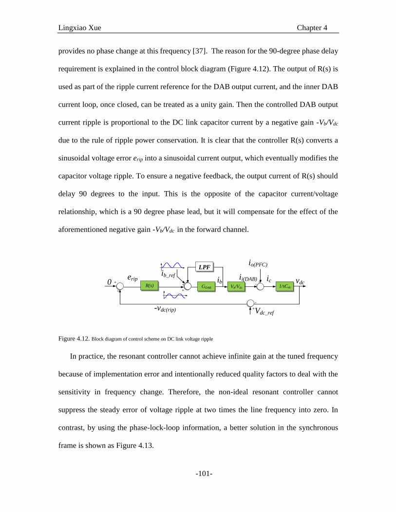
Lingxiao Xue Chapter 4
-101-
provides no phase change at this frequency [37]. The reason for the 90-degree phase delay
requirement is explained in the control block diagram (Figure 4.12). The output of R(s) is
used as part of the ripple current reference for the DAB output current, and the inner DAB
current loop, once closed, can be treated as a unity gain. Then the controlled DAB output
current ripple is proportional to the DC link capacitor current by a negative gain -Vb/Vdc
due to the rule of ripple power conservation. It is clear that the controller R(s) converts a
sinusoidal voltage error erip into a sinusoidal current output, which eventually modifies the
capacitor voltage ripple. To ensure a negative feedback, the output current of R(s) should
delay 90 degrees to the input. This is the opposite of the capacitor current/voltage
relationship, which is a 90 degree phase lead, but it will compensate for the effect of the
aforementioned negative gain -Vb/Vdc in the forward channel.
0
-vdc(rip)
Vb/Vdc
ii(DAB) vdc
ib_ref
-+ GDAB
ib- - +
io(PFC)
ic1/sCdcR(s)
-
+
+
Vdc_ref
+
+
LPF
erip
Figure 4.12. Block diagram of control scheme on DC link voltage ripple
In practice, the resonant controller cannot achieve infinite gain at the tuned frequency
because of implementation error and intentionally reduced quality factors to deal with the
sensitivity in frequency change. Therefore, the non-ideal resonant controller cannot
suppress the steady error of voltage ripple at two times the line frequency into zero. In
contrast, by using the phase-lock-loop information, a better solution in the synchronous
frame is shown as Figure 4.13.
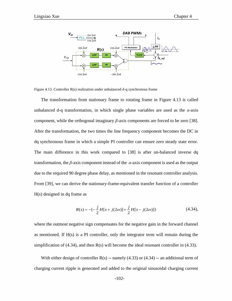
Lingxiao Xue Chapter 4
-102-
PILPF
Hi1(s) +-
LPF
ib_ref
PS Modulator
PLL
sin 2 t
+
Io0
Io
mIo
Vac
PILPF
-
-
DAB PWMsib
erip
cos 2 t sin 2 t
cos 2 t
cos 2 t
sin 2 t
R(s)
Figure 4.13. Controller R(s) realization under unbalanced d-q synchronous frame
The transformation from stationary frame to rotating frame in Figure 4.13 is called
unbalanced d-q transformation, in which single phase variables are used as the α-axis
component, while the orthogonal imaginary β-axis components are forced to be zero [38].
After the transformation, the two times the line frequency component becomes the DC in
dq synchronous frame in which a simple PI controller can ensure zero steady state error.
The main difference in this work compared to [38] is after un-balanced inverse dq
transformation, the β-axis component instead of the α-axis component is used as the output
due to the required 90 degree phase delay, as mentioned in the resonant controller analysis.
From [39], we can derive the stationary-frame-equivalent transfer function of a controller
H(s) designed in dq frame as
( ) [ (2 )] [ (2 )]2 2
j jR s H s j H s j (4.34),
where the outmost negative sign compensates for the negative gain in the forward channel
as mentioned. If H(s) is a PI controller, only the integrator term will remain during the
simplification of (4.34), and then R(s) will become the ideal resonant controller in (4.33).
With either design of controller R(s) -- namely (4.33) or (4.34) -- an additional term of
charging current ripple is generated and added to the original sinusoidal charging current

Lingxiao Xue Chapter 4
-103-
reference. This extra charging current ripple will cancel the effect of converter loss, and
further reduce the DC link voltage ripple, whose spectrum is dominant at two times the line
frequency.
4.2.4. Experimental Results
Two proof-of-concept battery charger prototypes were built with Si super junction
MOSFETs and enhancement-mode Gallium Nitride multi-chip modules [40]. The circuit
parameters are listed in Table 4.2.. A Delfino C28343 DSP control card from Texas
Instruments is used to realize the digital control system. The testing condition of the GaN
charger is different from the Si charger because of the GaN device maximum voltage
limitation [41].
Table 4.2. Prototype Parameters
Si charger GaN charger
AC voltage (V) 240 150
DC link voltage (V) 400 250
Battery voltage (V) 366 250
Output power (W) 1000 1000
Switching frequency (kHz) 50 500
Transformer turns ratio 1.1:1 1:1
DC link capacitance (µF) 40 85
Closed-loop control strategies with and without direct DC link control were both
applied. The AC-DC stage used a slow voltage loop to control the average of the DC link
voltage and employed a fast current loop to correct the power factor, as shown in Figure
4.11. The DAB current loop control used a first order filter and a PI controller. A full
system test with FB AC-DC stage and DAB DC-DC stage was carried out. Figure 4.14 and
Figure 4.15 show the experimental results of DC charging and pure sinusoidal charging on
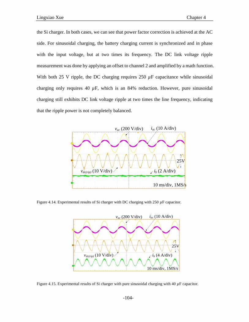
Lingxiao Xue Chapter 4
-104-
the Si charger. In both cases, we can see that power factor correction is achieved at the AC
side. For sinusoidal charging, the battery charging current is synchronized and in phase
with the input voltage, but at two times its frequency. The DC link voltage ripple
measurement was done by applying an offset to channel 2 and amplified by a math function.
With both 25 V ripple, the DC charging requires 250 µF capacitance while sinusoidal
charging only requires 40 µF, which is an 84% reduction. However, pure sinusoidal
charging still exhibits DC link voltage ripple at two times the line frequency, indicating
that the ripple power is not completely balanced.
vac (200 V/div) iac (10 A/div)
ib (2 A/div)vdc(rip) (10 V/div)
10 ms/div, 1MS/s
25V
Figure 4.14. Experimental results of Si charger with DC charging with 250 µF capacitor.
vac (200 V/div) iac (10 A/div)
ib (4 A/div)vdc(rip) (10 V/div)
25V
10 ms/div, 1MS/s
Figure 4.15. Experimental results of Si charger with pure sinusoidal charging with 40 µF capacitor.
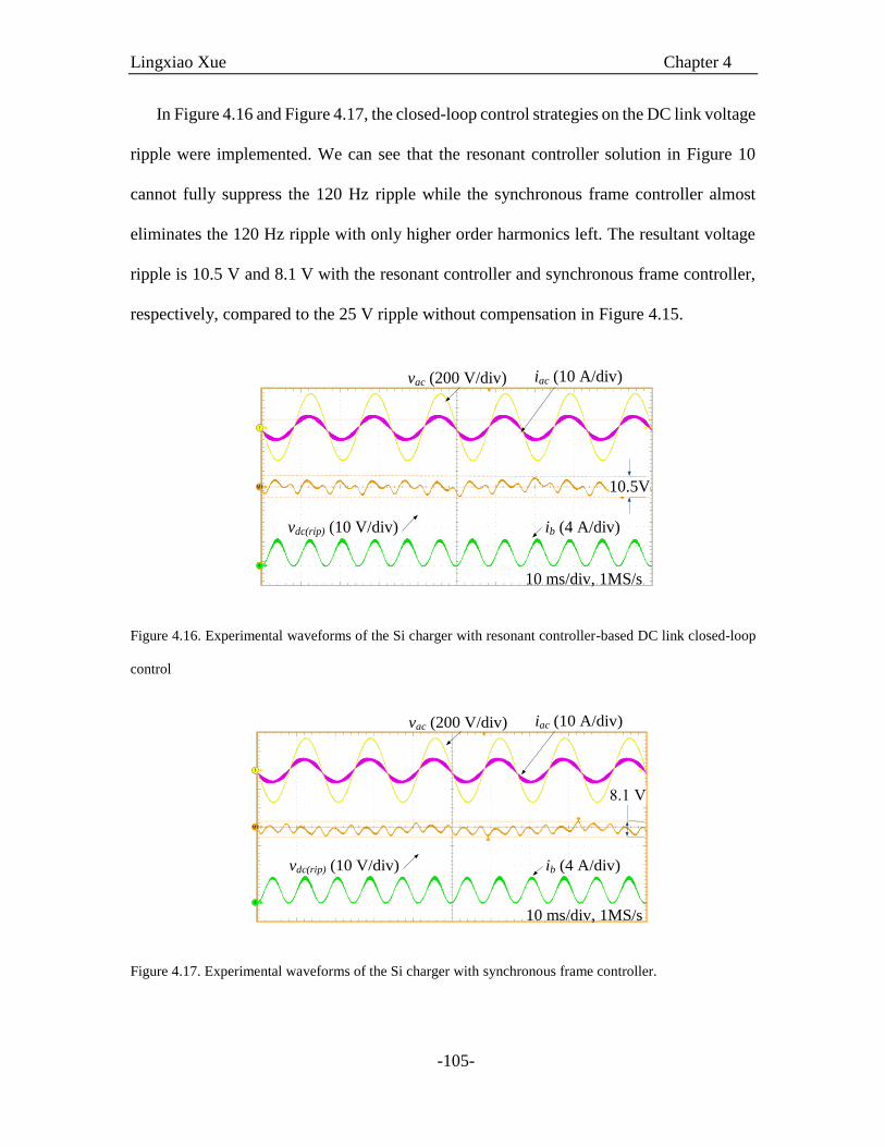
Lingxiao Xue Chapter 4
-105-
In Figure 4.16 and Figure 4.17, the closed-loop control strategies on the DC link voltage
ripple were implemented. We can see that the resonant controller solution in Figure 10
cannot fully suppress the 120 Hz ripple while the synchronous frame controller almost
eliminates the 120 Hz ripple with only higher order harmonics left. The resultant voltage
ripple is 10.5 V and 8.1 V with the resonant controller and synchronous frame controller,
respectively, compared to the 25 V ripple without compensation in Figure 4.15.
vac (200 V/div) iac (10 A/div)
ib (4 A/div)vdc(rip) (10 V/div)
10.5V
10 ms/div, 1MS/s
Figure 4.16. Experimental waveforms of the Si charger with resonant controller-based DC link closed-loop
control
vac (200 V/div) iac (10 A/div)
ib (4 A/div)vdc(rip) (10 V/div)
10 ms/div, 1MS/s
Figure 4.17. Experimental waveforms of the Si charger with synchronous frame controller.
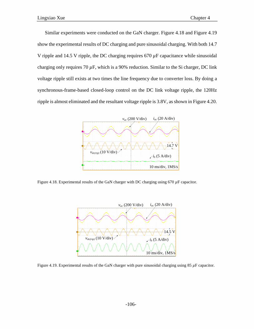
Lingxiao Xue Chapter 4
-106-
Similar experiments were conducted on the GaN charger. Figure 4.18 and Figure 4.19
show the experimental results of DC charging and pure sinusoidal charging. With both 14.7
V ripple and 14.5 V ripple, the DC charging requires 670 µF capacitance while sinusoidal
charging only requires 70 µF, which is a 90% reduction. Similar to the Si charger, DC link
voltage ripple still exists at two times the line frequency due to converter loss. By doing a
synchronous-frame-based closed-loop control on the DC link voltage ripple, the 120Hz
ripple is almost eliminated and the resultant voltage ripple is 3.8V, as shown in Figure 4.20.
vac (200 V/div) iac (20 A/div)
ib (5 A/div)vdc(rip) (10 V/div)
10 ms/div, 1MS/s
14.7 V
Figure 4.18. Experimental results of the GaN charger with DC charging using 670 µF capacitor.
vac (200 V/div) iac (20 A/div)
ib (5 A/div)vdc(rip) (10 V/div)
10 ms/div, 1MS/s
14.5 V
Figure 4.19. Experimental results of the GaN charger with pure sinusoidal charging using 85 µF capacitor.

Lingxiao Xue Chapter 4
-107-
vac (200 V/div) iac (20 A/div)
ib (5 A/div)vdc(rip) (10 V/div)
10 ms/div, 1MS/s
3.8 V
Figure 4.20. Experimental waveforms of the GaN charger using a rotating frame controller.
4.2.5. Summary and Conclusion
In a PHEV battery charger, the DC link capacitor occupies a large portion of the total
volume, even if other passive components can be significantly shrunk by using wide band
gap semiconductor devices at high frequency, mainly because the required capacitance is
largely determined by ripple power at two times the line frequency. In this section, a
sinusoidal charging scheme was proposed to reduce the DC link capacitance by balancing
the ripple power from input and output. The current controller design of a Dual Active
Bridge DC-DC converter is given to realize the sinusoidal charging. Experimental results
on both Si and GaN chargers verified the effectiveness of the controller design to
significantly suppress the DC link voltage ripple, but also revealed that pure sinusoidal
charging control cannot eliminate the DC link voltage ripple. In addressing this
shortcoming, the converter loss model was derived. It was found that the converter loss
with sinusoidal charging has a DC component and also a second-order harmonic
component, whose difference results in ripple energy in the DC link capacitors.

Lingxiao Xue Chapter 4
-108-
To fully compensate for the imbalance, and as an improvement over the sinusoidal
charging case, a closed-loop control is proposed to directly control the DC link voltage
ripple. To achieve zero steady-state error at two times the line frequency, both resonant-
controller-based and rotating-frame-based control schemes are analyzed. Different from
the traditional resonant controller and rotating frame control, the implemented controller
has to be phase-shifted by 90 degrees for the best steady state and transient performance.
Furthermore, rotating frame control can provide higher gain than the resonant controller,
due to the implementation error of the latter.
Two experimental prototypes, one with Si MOSFETS and one with a GaN multi-chip
module, both comprising a single-phase PFC and a DC-DC DAB converter, were built to
verify the analysis. Compared to DC charging, a sinusoidal charging scheme can reduce
the DC capacitance by 84% and 90% for the Si charger and the GaN charger, respectively.
The rotating frame controller can eliminate the DC link voltage ripple at the tuned
frequency, leaving only the higher order harmonics in the DC link voltage. In contrast, the
resonant controller cannot fully suppress the 120 Hz ripple because of the limited gain
caused by implementation error.
Sinusoidal charging can reduce the DC link capacitor but brings with it the drawback
of increased converter loss due to increased conduction loss and switching loss. However,
the controllability of the demonstrated method on the output current affords the chance to
optimize the charging current waveform shape for a better trade-off between DC
capacitance and charger efficiency. This will be examined in the next section.
4.3. ADVANCED CHARGING WAVEFORM EVALUATION
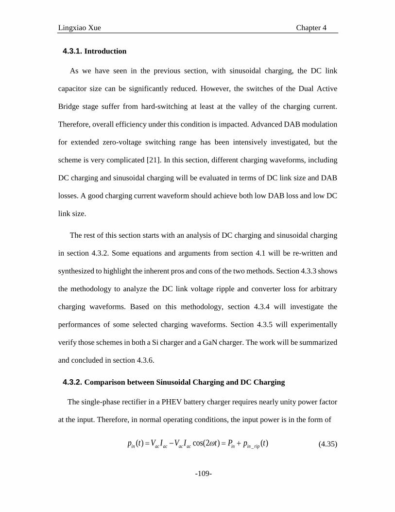
Lingxiao Xue Chapter 4
-109-
4.3.1. Introduction
As we have seen in the previous section, with sinusoidal charging, the DC link
capacitor size can be significantly reduced. However, the switches of the Dual Active
Bridge stage suffer from hard-switching at least at the valley of the charging current.
Therefore, overall efficiency under this condition is impacted. Advanced DAB modulation
for extended zero-voltage switching range has been intensively investigated, but the
scheme is very complicated [21]. In this section, different charging waveforms, including
DC charging and sinusoidal charging will be evaluated in terms of DC link size and DAB
losses. A good charging current waveform should achieve both low DAB loss and low DC
link size.
The rest of this section starts with an analysis of DC charging and sinusoidal charging
in section 4.3.2. Some equations and arguments from section 4.1 will be re-written and
synthesized to highlight the inherent pros and cons of the two methods. Section 4.3.3 shows
the methodology to analyze the DC link voltage ripple and converter loss for arbitrary
charging waveforms. Based on this methodology, section 4.3.4 will investigate the
performances of some selected charging waveforms. Section 4.3.5 will experimentally
verify those schemes in both a Si charger and a GaN charger. The work will be summarized
and concluded in section 4.3.6.
4.3.2. Comparison between Sinusoidal Charging and DC Charging
The single-phase rectifier in a PHEV battery charger requires nearly unity power factor
at the input. Therefore, in normal operating conditions, the input power is in the form of
_( ) cos(2 ) ( )in ac ac ac ac in in ripp t V I V I t P p t (4.35)

Lingxiao Xue Chapter 4
-110-
where pin(t) is the instantaneous input power at the AC input. Vac and Iac are the RMS
values of the AC side voltage and current, respectively, and ω is the line frequency in rad/s.
It is clear that the input power has both DC and double line frequency components. In
conventional charging methods, the output of the battery charger provides only DC power
as (4.36) in a lossless condition:
( ) ( )o dc inp t P (4.36)
In this section, unlike the previous section, the ripple power balance is analyzed under
a lossless assumption because in all other charging waveforms under examination except
the sinusoidal charging, the ripple power imbalance caused by the converter loss is
negligible compared to that caused by the charging waveform.
The DC component of the input power balances with the output power, but the ripple
power oscillating at two times the line frequency, designated as in (4.35), should be stored
in passive components between the AC source and the DC output. In most cases, an
intermediate bulk capacitor is used. Then the voltage ripple across the DC link capacitor
will be
ac ac
dc
dc dc
V IV
C V
(4.37)
In contrast, the output power of a sinusoidal charging in lossless conditions is described
as
(sin) ( ) ( )( ) cos(2 ) ( )o o avg bat o avg bat inp t I V I V t p t (4.38)
Lingxiao Xue Chapter 4
-111-
where Vb is the battery voltage and Io(avg) is the average value of the battery charging current.
With perfect balance between input power and output power, there’s no remaining ripple
power that needs to be stored. Therefore, the DC link voltage ripple will be zero.
0dcV (4.39)
Sinusoidal charging provides the ultimate extent to which the DC link voltage ripple
can be suppressed. DC charging waveform, together with all the other charging waveforms
that we will examine in later parts of this paper, always produce imbalanced ripple power.
Therefore, for those methods, the DC link voltage ripple at the double line frequency
cannot be eliminated.
Compared to DC charging, sinusoidal charging achieves a significant reduction of DC
link capacitance, but at the price of reduced converter efficiency. The main impact appears
in the efficiency of the DC/DC stage, since the AC/DC stage always deals with the same
format of power, regardless of charging current waveforms, as long as power factor
correction and DC voltage regulation are guaranteed. There are two factors that make the
DC/DC stage more lossy with sinusoidal charging: conduction loss and switching loss.
From (4.38) we can see that the DC/DC stage, with sinusoidal charging, needs to process
not only the DC power but also the ripple power at the double line frequency, increasing
the RMS value of the current through both semiconductor switches and transformer
windings. Therefore, it can be expected that the conduction loss of the DC/DC stage will
be higher.
What’s more, since the charging current will change from zero to two times the average
value in every double line cycle, it is harder to optimize the converter to achieve zero
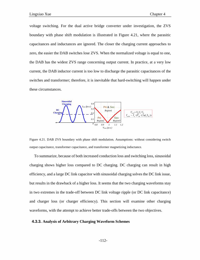
Lingxiao Xue Chapter 4
-112-
voltage switching. For the dual active bridge converter under investigation, the ZVS
boundary with phase shift modulation is illustrated in Figure 4.21, where the parasitic
capacitances and inductances are ignored. The closer the charging current approaches to
zero, the easier the DAB switches lose ZVS. When the normalized voltage is equal to one,
the DAB has the widest ZVS range concerning output current. In practice, at a very low
current, the DAB inductor current is too low to discharge the parasitic capacitances of the
switches and transformer; therefore, it is inevitable that hard-switching will happen under
these circumstances.
Vnom (p.u.)
Inom (p.u.)
0.8 0.9 1 1.10
0.1
0.2
0.3
0.4
1.2
Region 1
Region 2 Region 3
Pri & Sec
Pri Sec
Sinusoidal
Charging
DC
Charging
Figure 4.21. DAB ZVS boundary with phase shift modulation. Assumptions: without considering switch
output capacitance, transformer capacitance, and transformer magnetizing inductance.
To summarize, because of both increased conduction loss and switching loss, sinusoidal
charging shows higher loss compared to DC charging. DC charging can result in high
efficiency, and a large DC link capacitor with sinusoidal charging solves the DC link issue,
but results in the drawback of a higher loss. It seems that the two charging waveforms stay
in two extremes in the trade-off between DC link voltage ripple (or DC link capacitance)
and charger loss (or charger efficiency). This section will examine other charging
waveforms, with the attempt to achieve better trade-offs between the two objectives.
4.3.3. Analysis of Arbitrary Charging Waveform Schemes

Lingxiao Xue Chapter 4
-113-
The following analysis in this paper will assume lossless conditions. In fact, converter
losses contribute to ripple power imbalance and lead to DC link voltage ripple, as analyzed
in [24]. This is more obvious in ideal sinusoidal charging, in which most of the input ripple
power has been canceled out by the output ripple power. However, for all other charging
waveforms, including DC charging, due to the imbalance of ripple power between input
and output, the DC link voltage ripple is much higher than that of sinusoidal charging, so
the converter loss only contributes to a small portion of the overall voltage ripple. Therefore,
in this paper, all the ripple power analysis will assume lossless conditions, which greatly
simplifies the analytical derivation.
The charging current could be in any arbitrary waveform if it fulfills the following two
principles:
The average current equals to the value that the charging profile requires.
The double line frequency component of the waveform is in phase with the
input ripple power.
The first principle enforces the charging profile. Thus, different charging waveforms
will only mean different AC components, including the double line frequency component.
The second principle ensures that the output ripple power can cancel the input ripple power
so as to reduce the DC link energy storage requirement.
4.3.3.1. Methodology of DC Link Voltage Ripple Evaluation
The following derivation shows how to use ripple power balance to evaluate the DC
link voltage ripple given a charging current waveform. Given an arbitrary charging current
io(t), the output power po(t) will show a similar form because the battery voltage is a DC
value. Following principle 1 and 2, the output power can be written in the form of
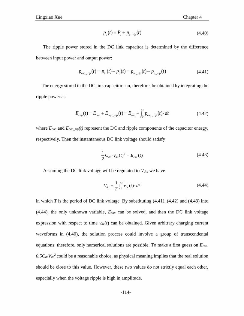
Lingxiao Xue Chapter 4
-114-
_( ) ( )o o o ripp t P p t (4.40)
The ripple power stored in the DC link capacitor is determined by the difference
between input power and output power:
_ _ _( ) ( ) ( ) ( ) ( )cap rip in o in rip o ripp t p t p t p t p t (4.41)
The energy stored in the DC link capacitor can, therefore, be obtained by integrating the
ripple power as
_ _0
( ) ( ) ( )t
cap con cap rip con cap ripE t E E t E p t dt (4.42)
where Econ and Ecap_rip(t) represent the DC and ripple components of the capacitor energy,
respectively. Then the instantaneous DC link voltage should satisfy
21( ) ( )
2dc dc capC v t E t (4.43)
Assuming the DC link voltage will be regulated to Vdc, we have
0
1( )
T
dc dcV v t dtT
(4.44)
in which T is the period of DC link voltage. By substituting (4.41), (4.42) and (4.43) into
(4.44), the only unknown variable, Econ can be solved, and then the DC link voltage
expression with respect to time vdc(t) can be obtained. Given arbitrary charging current
waveforms in (4.40), the solution process could involve a group of transcendental
equations; therefore, only numerical solutions are possible. To make a first guess on Econ,
0.5CdcVdc2 could be a reasonable choice, as physical meaning implies that the real solution
should be close to this value. However, these two values do not strictly equal each other,
especially when the voltage ripple is high in amplitude.
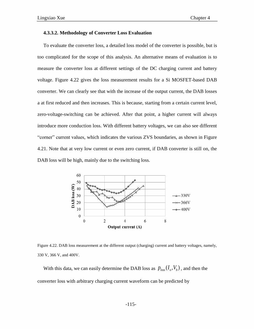
Lingxiao Xue Chapter 4
-115-
4.3.3.2. Methodology of Converter Loss Evaluation
To evaluate the converter loss, a detailed loss model of the converter is possible, but is
too complicated for the scope of this analysis. An alternative means of evaluation is to
measure the converter loss at different settings of the DC charging current and battery
voltage. Figure 4.22 gives the loss measurement results for a Si MOSFET-based DAB
converter. We can clearly see that with the increase of the output current, the DAB losses
a at first reduced and then increases. This is because, starting from a certain current level,
zero-voltage-switching can be achieved. After that point, a higher current will always
introduce more conduction loss. With different battery voltages, we can also see different
“corner” current values, which indicates the various ZVS boundaries, as shown in Figure
4.21. Note that at very low current or even zero current, if DAB converter is still on, the
DAB loss will be high, mainly due to the switching loss.
Figure 4.22. DAB loss measurement at the different output (charging) current and battery voltages, namely,
330 V, 366 V, and 400V.
With this data, we can easily determine the DAB loss as ( , )loss o bp I V , and then the
converter loss with arbitrary charging current waveform can be predicted by

Lingxiao Xue Chapter 4
-116-
0
1( ) [ (t), ]
T
loss b loss o bP V p i V dtT
(4.45)
Although, theoretically, the charging current waveform could be in any shape, patterns
that could potentially achieve a better trade-off between voltage ripple and converter loss
are preferred. In the following section, we will give some examples of charging current
waveforms.
4.3.4. Performance Prediction of Selected Charging Schemes
In this section, we will propose five different types of charging schemes with different
charging current waveforms. Those schemes will be evaluated in terms of DAB converter
loss and resultant DC link voltage ripple. The best scheme should have both low loss and
low DC link voltage ripple, so both high efficiency and low DC link capacitor size can be
achieved.
From the analysis of sinusoidal charging, we learned that increased loss is caused by
large ripple, leading to both high RMS current and higher switching loss. Therefore, it is
natural to think about reducing the ripple amplitude of the sinusoidal charging waveform
for better efficiency while keeping in mind the drawback of increased ripple power at
double line frequency in the DC link capacitor. The most straightforward scheme is the
reduced-ripple sinusoidal charging scheme, as shown in Figure 4.23(a). Compared to
conventional sinusoidal charging, it reduces only the ripple amplitude. This charging
current pattern is defined as
( ) ( ) ( )( ) cos(2 )o red rip o avg o avgi t I h I t (4.46)
in which h is the ripple index, defined as the ratio of ripple amplitude to the average value:
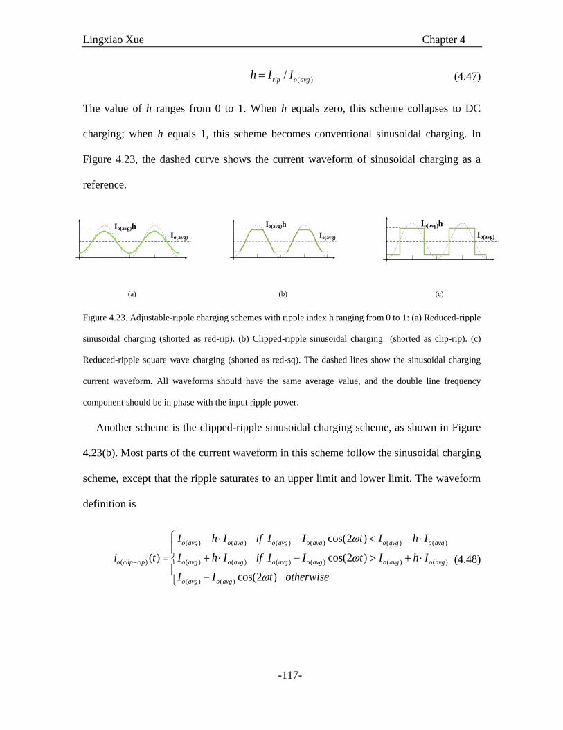
Lingxiao Xue Chapter 4
-117-
( )/rip o avgh I I (4.47)
The value of h ranges from 0 to 1. When h equals zero, this scheme collapses to DC
charging; when h equals 1, this scheme becomes conventional sinusoidal charging. In
Figure 4.23, the dashed curve shows the current waveform of sinusoidal charging as a
reference.
Io(avg)
Io(avg)h
Io(avg)
Io(avg)h
Io(avg)
Io(avg)h
(a) (b) (c)
Figure 4.23. Adjustable-ripple charging schemes with ripple index h ranging from 0 to 1: (a) Reduced-ripple
sinusoidal charging (shorted as red-rip). (b) Clipped-ripple sinusoidal charging (shorted as clip-rip). (c)
Reduced-ripple square wave charging (shorted as red-sq). The dashed lines show the sinusoidal charging
current waveform. All waveforms should have the same average value, and the double line frequency
component should be in phase with the input ripple power.
Another scheme is the clipped-ripple sinusoidal charging scheme, as shown in Figure
4.23(b). Most parts of the current waveform in this scheme follow the sinusoidal charging
scheme, except that the ripple saturates to an upper limit and lower limit. The waveform
definition is
( ) ( ) ( ) ( ) ( ) ( )
( ) ( ) ( ) ( ) ( ) ( ) ( )
( ) ( )
cos(2 )
( ) cos(2 )
cos(2 )
o avg o avg o avg o avg o avg o avg
o clip rip o avg o avg o avg o avg o avg o avg
o avg o avg
I h I if I I t I h I
i t I h I if I I t I h I
I I t otherwise
(4.48)

Lingxiao Xue Chapter 4
-118-
Compared to the reduced-ripple sinusoidal charging, for the same h, this scheme will
cause less imbalance between input and output power because of the smaller area
difference from sinusoidal charging, as shown in Figure 4.23(b).
Another interesting scheme is reduced-ripple square wave charging, as shown in Figure
4.23(c). The definition is
( ) ( )
( )
( ) ( )
1 32
( ) 2 2o avg o avg
o red sq
o avg o avg
I h I if ti t
I h I otherwise
(4.49)
The current waveform of this method has two current levels and the duty cycle is 50%.
Note that all three schemes in Figure 4.23 collapse to DC charging when the ripple index
h drops to zero.
The reduced-ripple square wave charging becomes full square wave charging if h = 1.
In this case, the lower part of the charging current waveform will be zero. At this point, we
propose a scheme called square-zero-off charging, as shown in Figure 4.24 (a) where the
DAB stage is shut down at the zero part of the current. In this scheme, the square wave has
a 50% duty cycle, so the average current can only be adjusted by changing the high level
of the waveform. The square-zero-off charging current can be described mathematically as
( )
( )
1 32 2
( ) 2 2
0
o avg
o sq off
I if ti t
otherwise
(4.50)
By shutting down the DAB stage at the zero current interval, the converter can avoid a
great deal of energy loss. Otherwise, the DAB converter will only be circulating the energy,
causing loss without delivering any power to the load. An extended scheme of square-zero-
off charging is called PWM-zero-off charging and is shown in Figure 4.24(b). This scheme
Lingxiao Xue Chapter 4
-119-
keeps the high level of the current constant but adjusts the pulse width (or duty cycle) of
the wave to achieve a different average value. This waveform is defined as
( ) ( )
_
_ _( )
(1 ) 2 (1 )( )
0
o avg o avg
pwm pk
pwm pk pwm pko pwm off
I II if t
I Ii t
otherwise
(4.51)
OFF OFF OFF
Io(avg)
Io(avg)
Ipwm_pk
OFF OFFOFF
(a) (b)
Figure 4.24. Charging schemes with DAB turned-off when charging current is zero. (a) Square-zero-off
charging (shorted as sq-off). (b) PWM-zero-off charging (shorted as pwm-off). The dashed lines show the
sinusoidal charging current waveform. All waveforms should have the same average value, and the double
line frequency component should be in phase with the input ripple power.
With the methodology explained in section 4.3.3, the DAB loss can be predicted for
different charging schemes, different ripple indices, and different battery voltages. The
results are shown in Figure 4.25. First, it is clear that with the increase of the ripple index,
all reduced-ripple charging schemes result in higher converter loss, mainly because of
increased RMS current value and switching loss at the zero current part of the waveform.
Furthermore, reduced-ripple and cut-ripple charging collapse to DC charging when h = 0
and to sinusoidal charging when h = 1. This is also the reason that their curves merge at
both ends in all three figures. Reduced-square wave charging also becomes DC charging
when h = 0; therefore, its curve also merges with the other two reduced-ripple charging
schemes.

Lingxiao Xue Chapter 4
-120-
By shutting down the DAB stage at the zero current point, the losses of the square-zero-
off scheme (designated as the sq-off dot) and pwm-zero-off scheme both drop to be lower
than those of the reduced-ripple counterparts. The PWM-zero-off scheme results in the
lowest loss among all the charging schemes.
0 0.2 0.4 0.6 0.8 120
40
60
80
Ripple index: h
DA
B l
oss
(W
)
Red-sq
Clip-rip
Red-rip
Sq-offPWM-
off
0 0.2 0.4 0.6 0.8 120
40
60
80
Ripple index: h
Red-sq
Clip-rip
Red-rip
Sq-offPWM-
off
DA
B l
oss
(W
)
0 0.2 0.4 0.6 0.8 120
40
60
80
Ripple index: h
DA
B l
oss
(W
)
Red-sq
Clip-rip
Red-ripSq-offPWM-
off
(a) Vb = 330V (b) Vb = 366V (c) Vb = 400V
Figure 4.25. DAB loss evaluation results in different charging waveforms and different battery voltages. Test
condition: 400 V input, 1.26 kW output power, 50 kHz switching frequency. (a) Battery voltage is 330 V. (b)
Battery voltage is 366 V. (c) Battery voltage is 400 V. Losses in all reduced-ripple charging schemes are
plotted with respect to ripple index. Zero-off charging schemes are plotted only at h = 1 because they are
only possible with full ripple.
In the next step, we will evaluate the DC link voltage ripple using the methodology
established in section 4.3.3. Figure 4.26 plots the DC link voltage waveforms vdc(t) for
different charging schemes based on the solution of (4.44) . In the three reduced-ripple
charging schemes, the cases of ripple index h = 0.6 are shown as an example. In Figure
4.26(a), we can see that the voltage ripple in reduced-ripple sinusoidal charging is a
sinusoidal wave because the charging current only contains DC and double line frequency
components. In contrast, the voltage ripple in clipped-ripple sinusoidal charging has both
a flat top and a flat bottom, reflecting the output current shape. The voltage ripple of the
reduced-ripple square-wave charging shows multiple peaks and valleys at h = 0.6.
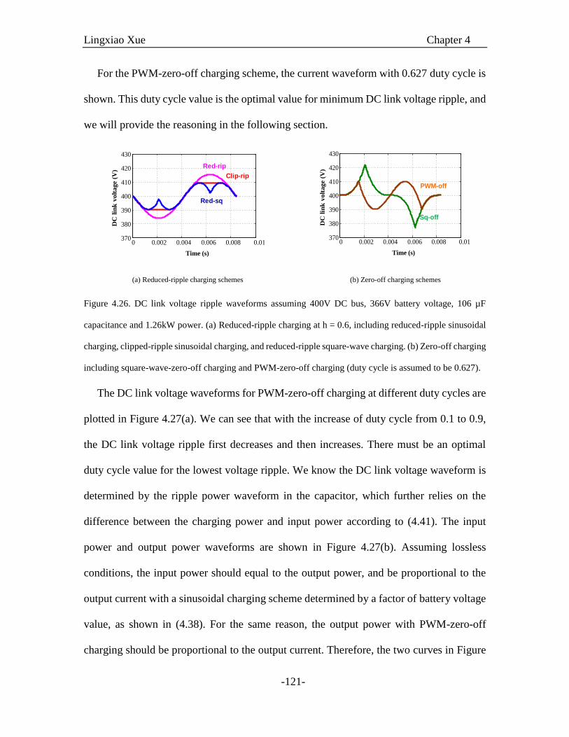
Lingxiao Xue Chapter 4
-121-
For the PWM-zero-off charging scheme, the current waveform with 0.627 duty cycle is
shown. This duty cycle value is the optimal value for minimum DC link voltage ripple, and
we will provide the reasoning in the following section.
0 0.002 0.004 0.006 0.008 0.01370
380
390
400
410
420
430
Time (s)
DC
lin
k v
olt
age (
V)
Red-sq
Clip-rip
Red-rip
0 0.002 0.004 0.006 0.008 0.01370
380
390
400
410
420
430
Time (s)
DC
lin
k v
olt
ag
e (
V)
Sq-off
PWM-off
(a) Reduced-ripple charging schemes (b) Zero-off charging schemes
Figure 4.26. DC link voltage ripple waveforms assuming 400V DC bus, 366V battery voltage, 106 µF
capacitance and 1.26kW power. (a) Reduced-ripple charging at h = 0.6, including reduced-ripple sinusoidal
charging, clipped-ripple sinusoidal charging, and reduced-ripple square-wave charging. (b) Zero-off charging
including square-wave-zero-off charging and PWM-zero-off charging (duty cycle is assumed to be 0.627).
The DC link voltage waveforms for PWM-zero-off charging at different duty cycles are
plotted in Figure 4.27(a). We can see that with the increase of duty cycle from 0.1 to 0.9,
the DC link voltage ripple first decreases and then increases. There must be an optimal
duty cycle value for the lowest voltage ripple. We know the DC link voltage waveform is
determined by the ripple power waveform in the capacitor, which further relies on the
difference between the charging power and input power according to (4.41). The input
power and output power waveforms are shown in Figure 4.27(b). Assuming lossless
conditions, the input power should equal to the output power, and be proportional to the
output current with a sinusoidal charging scheme determined by a factor of battery voltage
value, as shown in (4.38). For the same reason, the output power with PWM-zero-off
charging should be proportional to the output current. Therefore, the two curves in Figure
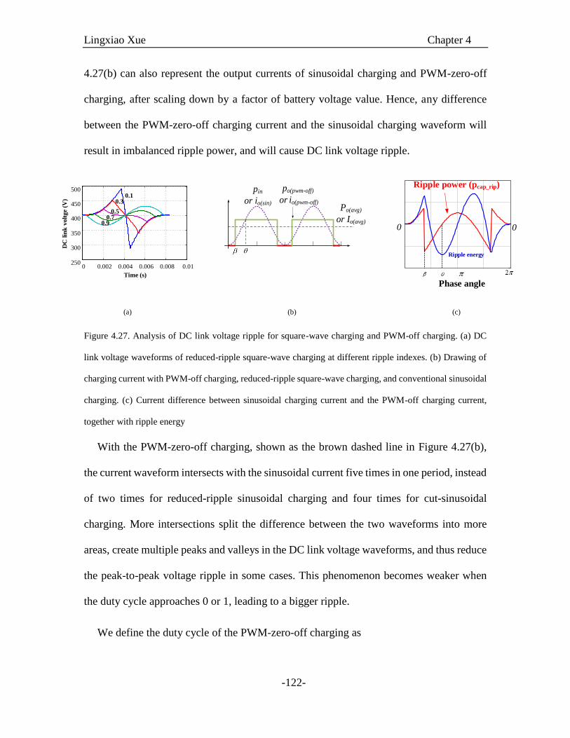
Lingxiao Xue Chapter 4
-122-
4.27(b) can also represent the output currents of sinusoidal charging and PWM-zero-off
charging, after scaling down by a factor of battery voltage value. Hence, any difference
between the PWM-zero-off charging current and the sinusoidal charging waveform will
result in imbalanced ripple power, and will cause DC link voltage ripple.
0 0.002 0.004 0.006 0.008 0.01250
300
350
400
450
500
0.1
0.3
0.50.7
0.9
DC
lin
k v
olt
ge (
V)
Time (s)
Po(avg)
or Io(avg)
po(pwm-off)
or io(pwm-off)
pin
or io(sin)
0
Phase angle
0
Ripple energy
Ripple power (pcap_rip)
(a) (b) (c)
Figure 4.27. Analysis of DC link voltage ripple for square-wave charging and PWM-off charging. (a) DC
link voltage waveforms of reduced-ripple square-wave charging at different ripple indexes. (b) Drawing of
charging current with PWM-off charging, reduced-ripple square-wave charging, and conventional sinusoidal
charging. (c) Current difference between sinusoidal charging current and the PWM-off charging current,
together with ripple energy
With the PWM-zero-off charging, shown as the brown dashed line in Figure 4.27(b),
the current waveform intersects with the sinusoidal current five times in one period, instead
of two times for reduced-ripple sinusoidal charging and four times for cut-sinusoidal
charging. More intersections split the difference between the two waveforms into more
areas, create multiple peaks and valleys in the DC link voltage waveforms, and thus reduce
the peak-to-peak voltage ripple in some cases. This phenomenon becomes weaker when
the duty cycle approaches 0 or 1, leading to a bigger ripple.
We define the duty cycle of the PWM-zero-off charging as

Lingxiao Xue Chapter 4
-123-
( ) _/o avg pwm pkD I I (4.52)
Then the phase angle β is determined by
(1 )D (4.53)
The phase angle θ at which the two waveforms intersect should satisfy
_ ( ) ( ) cos( )pwm pk o avg o avgI I I (4.54)
which is not related to battery voltage. In Figure 4.27(b) and Figure 4.27(c), from instant 0
to β, the sinusoidal wave is larger than the PWM wave, and, therefore, the ripple energy
will keep integrating until instant β when an energy valley is reached. From β to θ, since
the sinusoidal wave is lower than the PWM wave, the ripple energy, because of the integral,
will increase to a peak at instant θ. To minimize the DC link voltage ripple, we have to
make
(sin) ( ) (sin) ( )
0 0
( ) ( )o o pwm off o o pwm offi i d i i d
(4.55)
so that the ripple energy has the same amplitude but opposite signs at instant β and θ. A
numerical solution can be found for equation groups (4.52) to (4.55), which yields
0.627optD (4.56)
Note that both (4.54) and (4.55) can be normalized to the average output current Io(avg),
and the result in (4.56) will not change. This means that by selecting the duty cycle at 0.627
for the PWM-off charging, the DC link voltage ripple is at its minimum, regardless of
output power and battery voltage. The peak-to-peak DC link voltage ripple with different
charging schemes is then estimated using the method established in section 4.3.3. The

Lingxiao Xue Chapter 4
-124-
results at 1.26 kW output power are plotted in Figure 4.28. It is expected that with a larger
ripple index, both reduced-ripple and cut-ripple sinusoidal charging will result in a lower
ripple. When h = 1, theoretically, the voltage ripple will be zero because the ripple power
is fully balanced. Reduced-ripple square-wave charging exhibits a “U” shape curve with
an increase of the ripple index, because its current waveform intersects with the sinusoidal
charging current waveform six times, splitting the difference between the two waveforms
into more areas (Figure 4.23(c)). The achievable minimum DC link voltage ripple at around
h=0.7 is lower than the PWM-zero-off charging, as shown in Figure 4.28. Square-zero-off
charging shows the same voltage ripple as the reduced-ripple square wave charging when
h = 1, as expected. The PWM-off charging scheme in this figure uses the optimal duty
cycle of 0.627 and shows much lower voltage ripple than that of square-zero-off charging.
0
20
40
60
80
100
0 0.2 0.4 0.6 0.8 1
Red-sq
Clip-rip
Red-rip Sq-off
PWM-
off
Ripple index: h
DC
lin
k v
olt
ag
e
rip
ple
(V
)
Figure 4.28. Peak-to-peak ripple of the DC link voltage at different ripple index and charging schemes.
Conditions: 400 V DC bus, 106 µF capacitance and 1.26 kW power.
4.3.5. Experimental Results
To verify the proposed concept, two battery chargers were tested: one Si charger and
one GaN charger. In the experiments, the entire charger was tested, including both the
AC/DC stage and the DAB DC/DC stage, to verify both overall converter losses and DC
link voltage ripple. The test conditions of the Si charger and GaN charger are summarized
in Table I. Detailed information about the GaN charger can be found in [25].
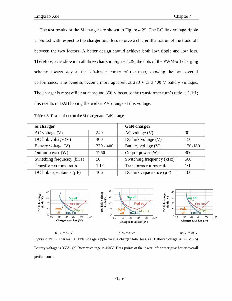
Lingxiao Xue Chapter 4
-125-
The test results of the Si charger are shown in Figure 4.29. The DC link voltage ripple
is plotted with respect to the charger total loss to give a clearer illustration of the trade-off
between the two factors. A better design should achieve both low ripple and low loss.
Therefore, as is shown in all three charts in Figure 4.29, the dots of the PWM-off charging
scheme always stay at the left-lower corner of the map, showing the best overall
performance. The benefits become more apparent at 330 V and 400 V battery voltages.
The charger is most efficient at around 366 V because the transformer turn’s ratio is 1.1:1;
this results in DAB having the widest ZVS range at this voltage.
Table 4.3. Test condition of the Si charger and GaN charger
Si charger GaN charger
AC voltage (V) 240 AC voltage (V) 90
DC link voltage (V) 400 DC link voltage (V) 150
Battery voltage (V) 330 - 400 Battery voltage (V) 120-180
Output power (W) 1260 Output power (W) 300
Switching frequency (kHz) 50 Switching frequency (kHz) 500
Transformer turns ratio 1.1:1 Transformer turns ratio 1:1
DC link capacitance (µF) 106 DC link capacitance (µF) 100
0
20
40
60
80
50 60 70 80 90 100
Charger total loss (W)
Red-rip
Sq-off
PWM-
off
DC
lin
k v
olt
ag
e
rip
ple
(V
)
Red-sq
Clip-rip
0
20
40
60
80
50 60 70 80 90 100
Charger total loss (W)
Red-rip
DC
lin
k v
olt
ag
e
rip
ple
(V
)
Red-sq
Clip-rip
Sq-off
PWM-
off
0
20
40
60
80
50 60 70 80 90 100
Charger total loss (W)
Red-rip
DC
lin
k v
olt
ag
e
rip
ple
(V
)
Red-sq
Clip-rip
Sq-off
PWM-
off
(a) Vb = 330V (b) Vb = 366V (c) Vb = 400V
Figure 4.29. Si charger DC link voltage ripple versus charger total loss. (a) Battery voltage is 330V. (b)
Battery voltage is 366V. (c) Battery voltage is 400V. Data points at the lower-left corner give better overall
performance.

Lingxiao Xue Chapter 4
-126-
Figure 4.29 also shows that the best two charging schemes are PWM-off and reduced-
ripple charging; therefore, these two methods were tested on the GaN charger. In the two
tests, the DC link voltage ripple was kept the same (around 13 V), and the converter losses
were measured. It can be seen from Figure 4.30 that PWM-off charging saved almost 39%
loss, boosting the converter efficiency by 2.3%.
(a) Reduced-ripple sinusoidal charging (b) PWM-off charging
Figure 4.30. GaN charger testing results at 150 V battery voltage and 300 W output power. (a) Reduced-
ripple charging. (b) PWM-off charging. The ripple voltage was kept the same (around 13 V) in two cases.
Efficiency is measured by Yokogawa power analyzer.
Figure 4.31 shows the testing waveforms of the drain-to-source voltages of GaN
switches: one from the primary side of the transformer, the other from the secondary side.
The zoomed-in waveform shows that ZVS is achieved at the top of the PWM-off charging
current. Additional tests were carried out at other battery voltages. Measurement results
show that, given the same DC link voltage ripple, PWM-off charging can reduce charger
loss by 21% at 120V battery voltage, and by 37% at 180V battery voltage, compared to
reduced-ripple sinusoidal charging.
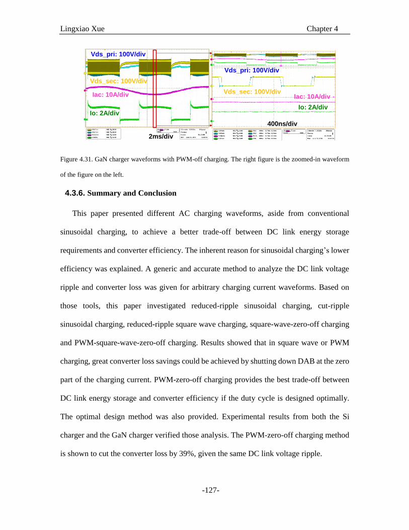
Lingxiao Xue Chapter 4
-127-
Figure 4.31. GaN charger waveforms with PWM-off charging. The right figure is the zoomed-in waveform
of the figure on the left.
4.3.6. Summary and Conclusion
This paper presented different AC charging waveforms, aside from conventional
sinusoidal charging, to achieve a better trade-off between DC link energy storage
requirements and converter efficiency. The inherent reason for sinusoidal charging’s lower
efficiency was explained. A generic and accurate method to analyze the DC link voltage
ripple and converter loss was given for arbitrary charging current waveforms. Based on
those tools, this paper investigated reduced-ripple sinusoidal charging, cut-ripple
sinusoidal charging, reduced-ripple square wave charging, square-wave-zero-off charging
and PWM-square-wave-zero-off charging. Results showed that in square wave or PWM
charging, great converter loss savings could be achieved by shutting down DAB at the zero
part of the charging current. PWM-zero-off charging provides the best trade-off between
DC link energy storage and converter efficiency if the duty cycle is designed optimally.
The optimal design method was also provided. Experimental results from both the Si
charger and the GaN charger verified those analysis. The PWM-zero-off charging method
is shown to cut the converter loss by 39%, given the same DC link voltage ripple.
Vds_pri: 100V/div
Vds_sec: 100V/div
Iac: 10A/div
Io: 2A/div
2ms/div
400ns/div
Vds_pri: 100V/div
Vds_sec: 100V/divIac: 10A/div
Io: 2A/div

Lingxiao Xue Chapter 4
-128-
4.4. SUMMARY AND CONCLUSION
In a PHEV battery charger, the DC link capacitor occupies a large portion of the total
volume, even if other passive components can be significantly shrunk by using wide band
gap semiconductor devices at high frequency, mainly because the required capacitance is
largely determined by ripple power at two times the line frequency. In this paper, sinusoidal
charging scheme was proposed to reduce the DC link capacitance by balancing the ripple
power from input and output.
Sinusoidal charging control strategies of DAB are proposed and implemented by a
closed-loop current control. Experimental results on both Si and GaN chargers verified the
effectiveness of the DAB current controller design to significantly suppress the DC link
voltage ripple, but also revealed that pure sinusoidal charging control cannot eliminate the
DC link voltage ripple. In addressing this shortcoming, the converter loss model was
derived. It was found that the converter loss with sinusoidal charging has a DC component
and also a second-order harmonic component, whose difference results in ripple energy in
the DC link capacitors.
To fully compensate for the imbalance, and as an improvement over the sinusoidal
charging case, a closed-loop control is proposed to directly control the DC link voltage
ripple. To achieve zero steady-state error at two times the line frequency, both resonant-
controller-based and rotating-frame-based control schemes are analyzed. Different from
the traditional resonant controller and rotating frame control, the implemented controller
has to be phase-shifted by 90 degrees for the best steady state and transient performance.
Furthermore, rotating frame control can provide higher gain than the resonant controller,
due to the implementation error of the latter.
Lingxiao Xue Chapter 4
-129-
Compared to DC charging, a sinusoidal charging scheme can reduce the DC
capacitance by 84% and 90% for the Si charger and the GaN charger, respectively. The
rotating frame controller can eliminate the DC link voltage ripple at the tuned frequency,
leaving only the higher order harmonics in the DC link voltage. In contrast, the resonant
controller cannot fully suppress the 120 Hz ripple because of the limited gain caused by
implementation error.
Sinusoidal charging can reduce the DC link capacitor but brings with it the drawback
of increased converter loss due to increased conduction loss and switching loss. However,
the controllability of the demonstrated method on the output current affords the chance to
optimize the charging current waveform shape for a better trade-off between DC
capacitance and charger efficiency. Different AC charging waveforms, aside from
conventional sinusoidal charging, were presented to achieve a better trade-off between DC
link energy storage requirements and converter efficiency. The inherent reason for
sinusoidal charging’s lower efficiency was explained. A generic and accurate method to
analyze the DC link voltage ripple and converter loss was given for arbitrary charging
current waveforms. Based on those tools, this paper investigated reduced-ripple sinusoidal
charging, cut-ripple sinusoidal charging, reduced-ripple square wave charging, square-
wave-zero-off charging, and PWM-square-wave-zero-off charging. Results showed that
great converter loss savings could be achieved by shutting down DAB at the zero part of
the charging current. PWM-zero-off charging provides the best trade-off between DC link
energy storage and converter efficiency if the duty cycle is designed optimally. The optimal
design method was also provided. Experimental results from both the Si charger and the
Lingxiao Xue Chapter 4
-130-
GaN charger verified those analyses. The PWM-zero-off charging method is shown to cut
the converter loss by 39%, given the same DC link voltage ripple.
4.5. LIST OF REFERENCES
[1] M. Yilmaz and P. T. Krein, "Review of Battery Charger Topologies, Charging
Power Levels, and Infrastructure for Plug-In Electric and Hybrid Vehicles," IEEE
Trans. Power Electron., vol. 28, no. 5, pp. 2151-2169, 2013.
[2] B. Whitaker, A. Barkley, Z. Cole, B. Passmore, D. Martin, T. McNutt, et al., "A
High-Density, High-Efficiency, Isolated On-Board Vehicle Battery Charger
Utilizing Silicon Carbide Power Devices," IEEE Trans. Power Electron., vol. PP,
no. 99, pp. 1-1, 2013.
[3] G. Linlin, R. Xinbo, X. Ming, and Y. Kai, "Means of Eliminating Electrolytic
Capacitor in AC/DC Power Supplies for LED Lightings," IEEE Trans. Power
Electron., vol. 24, no. 5, pp. 1399-1408, 2009.
[4] W. Beibei, R. Xinbo, Y. Kai, and X. Ming, "A Method of Reducing the Peak-to-
Average Ratio of LED Current for Electrolytic Capacitor-Less AC–DC
Drivers," IEEE Trans. Power Electron., vol. 25, no. 3, pp. 592-601, 2010.
[5] T. Shimizu, Y. Jin, and G. Kimura, "DC ripple current reduction on a single-phase
PWM voltage-source rectifier," IEEE Trans. Ind. Appl., vol. 36, no. 5, pp. 1419-
1429, 2000.
[6] Y. X. Qin, H. S. H. Chung, D. Y. Lin, and S. Y. R. Hui, "Current source ballast for
high power lighting emitting diodes without electrolytic capacitor," in Proc. Ann.
Conf. IEEE Ind. Electron., 2008, pp. 1968-1973.
[7] W. Ruxi, F. Wang, D. Boroyevich, R. Burgos, L. Rixin, N. Puqi, et al., "A High
Power Density Single-Phase PWM Rectifier With Active Ripple Energy Storage,"
IEEE Trans. Power Electron., vol. 26, no. 5, pp. 1430-1443, 2011.
[8] D. Dong, I. Cvetkovic, D. Boroyevich, W. Zhang, R. Wang, and P. Mattavelli,
"Grid-Interface Bidirectional Converter for Residential DC Distribution Systems
Part One: High-Density Two-Stage Topology," IEEE Trans. Power Electron., vol.
28, no. 4, pp. 1655-1666, 2013.
[9] H. Haibing, S. Harb, N. H. Kutkut, Z. J. Shen, and I. Batarseh, "A Single-Stage
Microinverter Without Using Eletrolytic Capacitors," IEEE Trans. Power Electron.,
vol. 28, no. 6, pp. 2677-2687, 2013.
[10] T. Shimizu, T. Fujita, G. Kimura, and J. Hirose, "A unity power factor PWM
rectifier with DC ripple compensation," IEEE Trans. Ind. Electron., vol. 44, no. 4,
pp. 447-455, 1997.
[11] S. Yuxiang, L. Liming, L. Hui, and X. Yaosuo, "A single-phase grid-connected PV
converter with minimal DC-link capacitor and low-frequency ripple-free maximum
power point tracking," in Proc. IEEE Energy Convers. Congr. Expo., 2013, pp.
2385-2390.
Lingxiao Xue Chapter 4
-131-
[12] K. Tae-Hoon, J. Jin-Beom, L. Baek-Haeng, S. Dong-Hyun, S. Hyun-Sik, K.
Byoung-Hoon, et al., "Analytical study on low-frequency ripple effect of battery
charging," in Proc. IEEE Veh. Power Propulsion Conf.,, 2012, pp. 809-811.
[13] H. Z. Beh, G. A. Covic, and J. T. Boys, "Effects of pulse and DC charging on
lithium iron phosphate (LiFePO<inf>4</inf>) batteries," in Proc. IEEE Energy
Convers. Congr. Expo., 2013, pp. 315-320.
[14] S. Bala, T. Tengner, P. Rosenfeld, and F. Delince, "The effect of low frequency
current ripple on the performance of a Lithium Iron Phosphate (LFP) battery energy
storage system," in Proc. IEEE Energy Convers. Congr. Expo., 2012, pp. 3485-
3492.
[15] G. Venkataramanan, "A direct AC-DC converter for battery chargers," in Proc.
IEEE Power Electron. Spec. Conf., 1997, pp. 126-130 vol.1.
[16] M. G. Egan, D. L. O'Sullivan, J. G. Hayes, M. J. Willers, and C. P. Henze, "Power-
Factor-Corrected Single-Stage Inductive Charger for Electric Vehicle Batteries,"
IEEE Trans. Ind. Appl., vol. 54, no. 2, pp. 1217-1226, 2007.
[17] L. Siqi, D. Junjun, and C. C. Mi, "Single-Stage Resonant Battery Charger With
Inherent Power Factor Correction for Electric Vehicles," IEEE Trans. Veh.
Technol., vol. 62, no. 9, pp. 4336-4344, 2013.
[18] H.-J. Chae, H.-T. Moon, and J.-Y. Lee, "On-board battery charger for PHEV
without high-voltage electrolytic capacitor," Electron. Lett., vol. 46, no. 25, pp.
1691-1692, 2010.
[19] S. Y. Youn and J. Y. Lee, "Electrolytic-capacitor-less AC/DC electric vehicle on-
board battery charger for universal line applications," Electron. Lett., vol. 47, no.
13, pp. 768-770, 2011.
[20] C.-J. Shin and J.-Y. Lee, "An Electrolytic Capacitor-less Bi-directional EV On-
Board Charger using Harmonic Modulation Technique," IEEE Trans. Power
Electron., vol. PP, no. 99, pp. 1-1, 2013.
[21] J. Everts, F. Krismer, J. Van den Keybus, J. Driesen, and J. W. Kolar, "Optimal
ZVS Modulation of Single-Phase Single-Stage Bidirectional DAB
AC–DC Converters," IEEE Trans. Power Electron., vol. 29, no. 8, pp.
3954-3970, 2014.
[22] M. Rosekeit and R. W. De Doncker, "Smoothing power ripple in single phase
chargers at minimized dc-link capacitance," in Proc. IEEE 8th Int. Conf. Power
Electron. Energy Convers. Congr. Expo., 2011, pp. 2699-2703.
[23] X. Lingxiao, D. Diaz, S. Zhiyu, L. Fang, P. Mattavelli, and D. Boroyevich, "Dual
active bridge based battery charger for plug-in hybrid electric vehicle with charging
current containing low frequency ripple," in Proc. IEEE Appl. Power Electron.
Conf. Expo., 2013, pp. 1920-1925.
[24] X. Lingxiao, P. Mattavelli, D. Boroyevich, S. Zhiyu, and R. Burgos, "Closed-loop
control on DC link voltage ripple of plug-in hybrid electric vehicle charger with
sinusoidal charging," in Proc. IEEE Energy Convers. Congr. Expo., 2013, pp.
3607-3614.
[25] X. Lingxiao, S. Zhiyu, M. Mingkai, D. Boroyevich, R. Burgos, B. Hughes, et al.,
"Bi-directional PHEV battery charger based on normally-off GaN-on-Si multi-chip
module," in Proc. IEEE Appl. Power Electron. Conf. Expo., 2014, pp. 1662-1668.

Lingxiao Xue Chapter 4
-132-
[26] X. Lingxiao, P. Mattavelli, D. Boroyevich, B. Hughes, and R. Burgos, "Efficiency
optimized AC charging waveform for GaN bidirectional PHEV Battery Charger,"
in Proc. 16th Eur. Conf. Power Electron. Appl., 2014, pp. 1-10.
[27] L.-R. Chen, S.-L. Wu, D.-T. Shieh, and T.-R. Chen, "Sinusoidal ripple current
charging strategy and optimal charging frequency for Li-ion batteries," IEEE Trans.
Ind. Electron., vol. 60, no. 1, pp. 88-97, Jan 2013.
[28] Y. D. Lee and S. Y. Park, "Electrochemical State Based Sinusoidal Ripple Current
Charging Control," IEEE Trans. Power Electron., vol. PP, no. 99, pp. 1-1, 2014.
[29] R. W. A. A. De Doncker, D. M. Divan, and M. H. Kheraluwala, "A three-phase
soft-switched high-power-density DC/DC converter for high-power applications,"
IEEE Trans. Ind. Appl., vol. 27, no. 1, pp. 63-73, 1991.
[30] N. Tuan, L. KilHo, W. Jehyuk, and N. Kwanghee, "Study of single-phase
bidirectional battery charger for high power application," in Proc. Int. Power
Electron. and Motion Control Conf., 2012, pp. 958-962.
[31] F. Krismer and J. W. Kolar, "Accurate Small-Signal Model for the Digital Control
of an Automotive Bidirectional Dual Active Bridge," IEEE Trans. Power Electron.,
vol. 24, no. 12, pp. 2756-2768, 2009.
[32] N. Tuan, W. Jehyuk, and N. Kwanghee, "A single-phase bidirectional dual active
half-bridge converter," in Proc. IEEE Appl. Power Electron. Conf. Expo., 2012, pp.
1127-1133.
[33] T. Duong, Z. Haihua, and A. M. Khambadkone, "Energy management and dynamic
control in Composite Energy Storage System for micro-grid applications," in Proc.
Ann. Conf. IEEE Ind. Electron., 2010, pp. 1818-1824.
[34] H. Kim and K.-H. Kim, "Filter design for grid connected PV inverters," in IEEE
Int. Conf. Sustainable Energy Technol., 2008, pp. 1070-1075.
[35] P. Haaf and J. Harper, "Understanding diode reverse recovery and its effect on
switching losses," 2007.
[36] F. Krismer, "Modeling and optimization of bidirectional dual active bridge DC-DC
converter topologies," Ph.D. Dissertation, Eidgenössische Technische Hochschule
ETH Zürich, 2010.
[37] S. Fukuda and T. Yoda, "A novel current-tracking method for active filters based
on a sinusoidal internal model [for PWM invertors]," IEEE Trans. Ind. Appl., vol.
37, no. 3, pp. 888-895, 2001.
[38] D. Dong, T. Thacker, R. Burgos, W. Fei, and D. Boroyevich, "On Zero Steady-
State Error Voltage Control of Single-Phase PWM Inverters With Different Load
Types," IEEE Trans. Power Electron., vol. 26, no. 11, pp. 3285-3297, 2011.
[39] D. N. Zmood, D. G. Holmes, and G. H. Bode, "Frequency-domain analysis of three-
phase linear current regulators," IEEE Trans. Ind. Appl., vol. 37, no. 2, pp. 601-610,
2001.
[40] L. Fang, C. Zheng, X. Lingxiao, P. Mattavelli, D. Boroyevich, and B. Hughes,
"Design considerations for GaN HEMT multichip halfbridge module for high-
frequency power converters," in Proc. IEEE Appl. Power Electron. Conf. Expo.,
2014, pp. 537-544.
[41] B. Hughes, J. Lazar, S. Hulsey, M. Musni, D. Zehnder, A. Garrido, et al.,
"Normally-off GaN-on-Si multi-chip module boost converter with 96% efficiency

Lingxiao Xue Chapter 4
-133-
and low gate and drain overshoot," in Proc. IEEE Appl. Power Electron. Conf.
Expo., 2014, pp. 484-487.
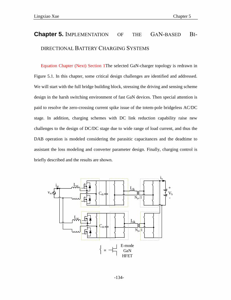
Lingxiao Xue Chapter 5
-134-
Chapter 5. IMPLEMENTATION OF THE GAN-BASED BI-
DIRECTIONAL BATTERY CHARGING SYSTEMS
Equation Chapter (Next) Section 1The selected GaN-charger topology is redrawn in
Figure 5.1. In this chapter, some critical design challenges are identified and addressed.
We will start with the full bridge building block, stressing the driving and sensing scheme
design in the harsh switching environment of fast GaN devices. Then special attention is
paid to resolve the zero-crossing current spike issue of the totem-pole bridgeless AC/DC
stage. In addition, charging schemes with DC link reduction capability raise new
challenges to the design of DC/DC stage due to wide range of load current, and thus the
DAB operation is modeled considering the parasitic capacitances and the deadtime to
assistant the loss modeling and converter parameter design. Finally, charging control is
briefly described and the results are shown.
Lac
Cdcvac
Nps:1
Llk +
-Vb
iac
io
Lac
Cdc
Nps:1
Llk
=
E-mode
GaN
HFET

Lingxiao Xue Chapter 5
-135-
Figure 5.1. Topology of GaN-based battery charger for plug-in hybrid electric vehicle
5.1. FULL BRIDGE BUILDING BLOCK DESIGN
As the charger topology shows, the full bridge is the basic function block of the power
stage. It can be configured as part of the AC/DC stage, or one side of the DAB DC/DC
stage. To achieve high power density and system-level integration, we proposed designing
the GaN full bridge as a “Power Electronics Building Block (PEBB)” to modularize the
final design of the charger. Each full bridge contains independent power supplies, GaN
drivers, EMI self-containment filters, and sensing circuits. This section will detail those
function blocks.
5.1.1. Driving Channel Design for the GaN MCM
5.1.1.1. The Requirement and Challenge of Driving Channel Design
Due to the integrated gate drivers, the driving loop is contained in the module so that
an external PWM signal source with relatively high output impedance can be directly used
to drive the gate driver in the module. However, to drive the half-bridge module, the
floating drive is still a necessity at least for the top switch. The floating drive for the high
dv/dt (100 V/ns) is challenging. In this work, the floating driving is realized by a
combination of an isolated DC/DC converter and a digital isolator to provide fast and
robust driving to the module, as shown in Figure 5.2. This solution can provide better
common-mode transient immunity (CMTI) than the pure bootstrap solution and the
optocoupler solution [1, 2]. Also, this solution provides a much wider duty cycle range,
which the bootstrap solution cannot achieve due to the bootstrap capacitor’s required
charging time.

Lingxiao Xue Chapter 5
-136-
The key to designing the driving channel with high CMTI is to provide a high
impedance between the high voltage/power side of the GaN MCM to the low power side
that comes from the control circuit. When the isolator and the power supply in Figure 5.2
are used to drive the top side switch in a half bridge, the potential of the output side will
swing with respect to the negative rail of the half bridge, due to the switching operation of
the bottom switch. This jumping potential becomes a noise source Vnoise applied between
the output side of the isolator and the negative rail of the half bridge. This noise current
will propagate through the isolation capacitance of the digital isolator and the power supply
(Cd and Cps), and the return path impedance Zg, whose value depends on how the negative
rail and the control ground are connected. As a result, a noise current is induced in this loop
and causes noise voltage across the impedances at the PWM signal side, which may corrupt
the signal. Note that the victim of this could be any logic circuits before the isolation barrier,
from the primary side of the isolator back to the PWM source (a DSP control platform, for
example). Very often we observed the PWM signals corrupted into a wrong logic level or
the control circuit begins to malfunction.
Digital
isolator
PWM To MCM
Isolated
Power supplyVcc Vdd
GND Vee
Cd
Cps
Zg
Vnoise
ISO
Vn
Figure 5.2. Driving scheme for the MCM: digital isolator plus isolated DC/DC converter
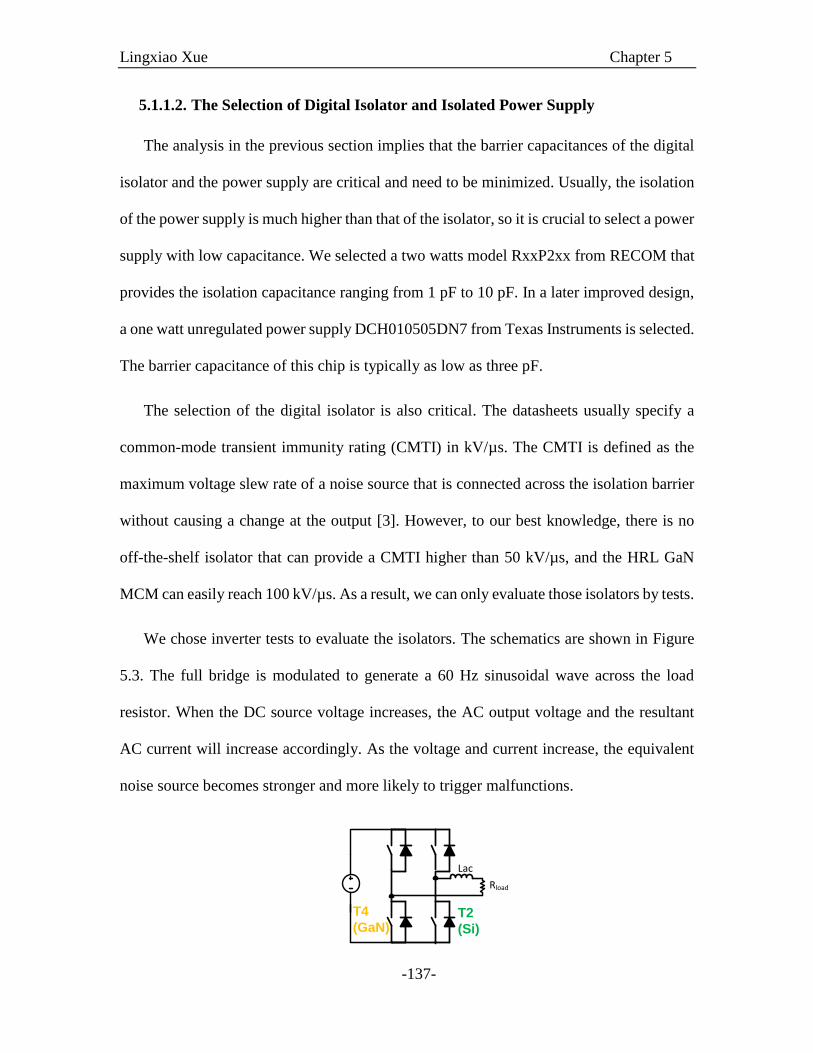
Lingxiao Xue Chapter 5
-137-
5.1.1.2. The Selection of Digital Isolator and Isolated Power Supply
The analysis in the previous section implies that the barrier capacitances of the digital
isolator and the power supply are critical and need to be minimized. Usually, the isolation
of the power supply is much higher than that of the isolator, so it is crucial to select a power
supply with low capacitance. We selected a two watts model RxxP2xx from RECOM that
provides the isolation capacitance ranging from 1 pF to 10 pF. In a later improved design,
a one watt unregulated power supply DCH010505DN7 from Texas Instruments is selected.
The barrier capacitance of this chip is typically as low as three pF.
The selection of the digital isolator is also critical. The datasheets usually specify a
common-mode transient immunity rating (CMTI) in kV/µs. The CMTI is defined as the
maximum voltage slew rate of a noise source that is connected across the isolation barrier
without causing a change at the output [3]. However, to our best knowledge, there is no
off-the-shelf isolator that can provide a CMTI higher than 50 kV/µs, and the HRL GaN
MCM can easily reach 100 kV/µs. As a result, we can only evaluate those isolators by tests.
We chose inverter tests to evaluate the isolators. The schematics are shown in Figure
5.3. The full bridge is modulated to generate a 60 Hz sinusoidal wave across the load
resistor. When the DC source voltage increases, the AC output voltage and the resultant
AC current will increase accordingly. As the voltage and current increase, the equivalent
noise source becomes stronger and more likely to trigger malfunctions.
Lac
Rload
T2
(Si)
T4
(GaN)
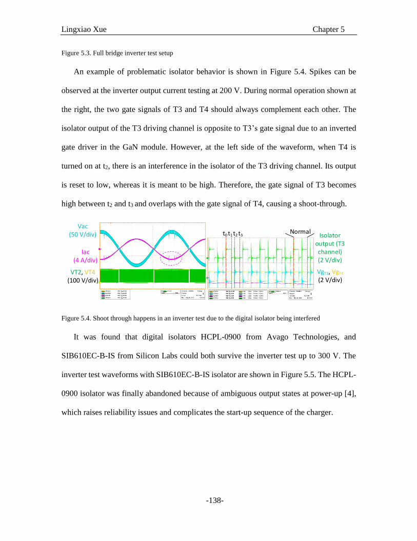
Lingxiao Xue Chapter 5
-138-
Figure 5.3. Full bridge inverter test setup
An example of problematic isolator behavior is shown in Figure 5.4. Spikes can be
observed at the inverter output current testing at 200 V. During normal operation shown at
the right, the two gate signals of T3 and T4 should always complement each other. The
isolator output of the T3 driving channel is opposite to T3’s gate signal due to an inverted
gate driver in the GaN module. However, at the left side of the waveform, when T4 is
turned on at t2, there is an interference in the isolator of the T3 driving channel. Its output
is reset to low, whereas it is meant to be high. Therefore, the gate signal of T3 becomes
high between t2 and t3 and overlaps with the gate signal of T4, causing a shoot-through.
Iac (4 A/div)
VT2, VT4(100 V/div)
VgT3, VgT4
(2 V/div)
Isolator output (T3 channel)(2 V/div)
t0 t1 t2 t3
Vac (50 V/div) Normal
Figure 5.4. Shoot through happens in an inverter test due to the digital isolator being interfered
It was found that digital isolators HCPL-0900 from Avago Technologies, and
SIB610EC-B-IS from Silicon Labs could both survive the inverter test up to 300 V. The
inverter test waveforms with SIB610EC-B-IS isolator are shown in Figure 5.5. The HCPL-
0900 isolator was finally abandoned because of ambiguous output states at power-up [4],
which raises reliability issues and complicates the start-up sequence of the charger.

Lingxiao Xue Chapter 5
-139-
Iac (4 A/div)
VT2, VT4(50 V/div)
Vac (50 V/div)
Figure 5.5. Inverter test at 300 V and 1 kW with SIB610EC-B-IS digital isolator
5.1.1.3. Bottom Switch Driving
It is reasonable to use the same driving schemes for both the top and bottom switches
in a half bridge, so the signal propagation delay for both channels will match with each
other. This will simplify the timing sequence design, especially considering the high
switching frequency design of GaN devices.
Furthermore, using the same driving schemes for both switches also helps the isolator
accommodate high voltage slew rate across the isolation barrier. In this way, the return
path impedance Zg in Figure 5.2 will be composed of the total barrier capacitance of the
isolator and the power supply, as shown in Figure 5.6. In contrast, if the PWM signal is
directly driving the bottom switch of the GaN module, that is to say, there is no isolation
between the control ground to the negative rail of the GaN module, then the return path
impedance Zg will be zero. In this case, the isolator is much easier to be interfered with by
the high dv/dt noise. By using two separate isolators to both top and bottom switches, the
dv/dt slew rate will be cut in half for each of the isolators, which helps the isolator survive
the high common mode noise generated by fast GaN switching.

Lingxiao Xue Chapter 5
-140-
Digital
isolator
PWM
Top
To MCM
Top Switch
Isolated
Power supply
Cd
Cps
Vnoise
ISO
PWM
Bottom
Cd
Cps
ISO
To MCM
Bottom Switch
Zg
Figure 5.6. Increasing return path impedance Zg by using the same driving scheme for both the top switch
and the bottom switch of the half bridge
5.1.1.4. Adding Filters for Noise Containment
When a digital isolator is used in the driving channel of the bottom switch, as described
in the previous section, the return path impedance through the driving circuit of the lower
switch becomes very high. This high impedance may make the noise current flow through
an alternative low impedance path if not designed properly. Figure 5.7 describes a situation
in which the DSP board and its associated grounding provide this low impedance path for
the noise to return (red dashed lines). The wired connection between the DSP board and
the full bridge board includes PWM signals, common ground, and power supply if the DSP
board supplies the full bridge.
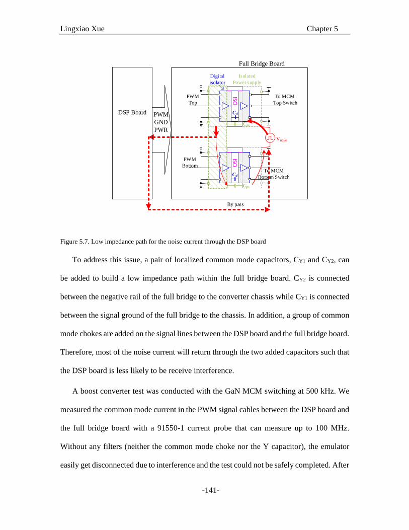
Lingxiao Xue Chapter 5
-141-
Digital
isolator
PWM
Top
To MCM
Top Switch
Isolated
Power supply
Cd
Cps
Vnoise
ISO
PWM
Bottom
Cd
Cps
ISOTo MCM
Bottom Switch
Full Bridge Board
DSP Board
By pass
PWM
GND
PWR
Figure 5.7. Low impedance path for the noise current through the DSP board
To address this issue, a pair of localized common mode capacitors, CY1 and CY2, can
be added to build a low impedance path within the full bridge board. CY2 is connected
between the negative rail of the full bridge to the converter chassis while CY1 is connected
between the signal ground of the full bridge to the chassis. In addition, a group of common
mode chokes are added on the signal lines between the DSP board and the full bridge board.
Therefore, most of the noise current will return through the two added capacitors such that
the DSP board is less likely to be receive interference.
A boost converter test was conducted with the GaN MCM switching at 500 kHz. We
measured the common mode current in the PWM signal cables between the DSP board and
the full bridge board with a 91550-1 current probe that can measure up to 100 MHz.
Without any filters (neither the common mode choke nor the Y capacitor), the emulator
easily get disconnected due to interference and the test could not be safely completed. After
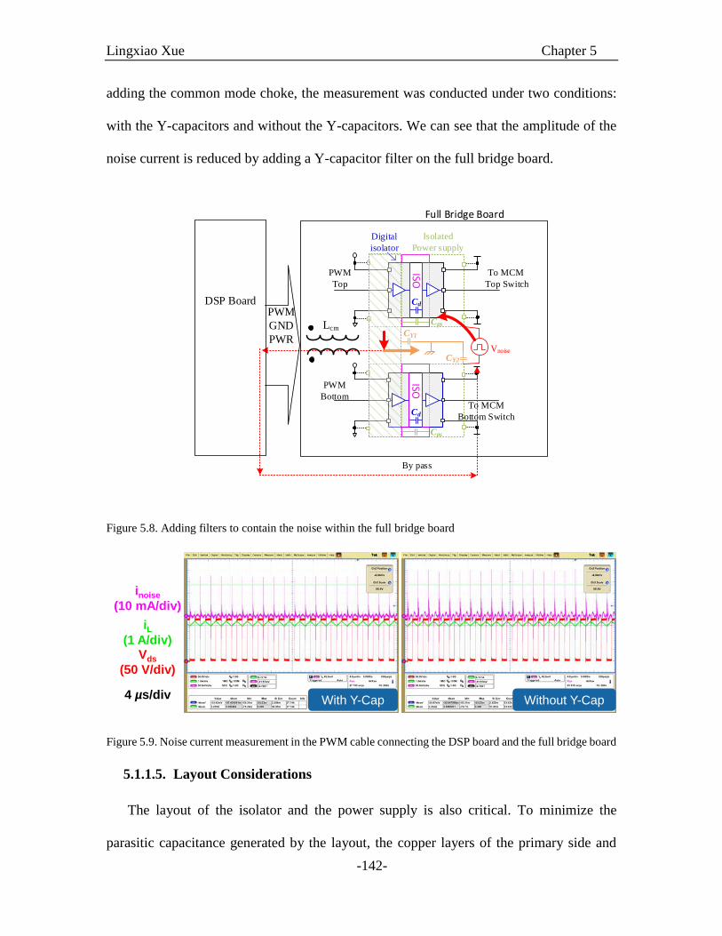
Lingxiao Xue Chapter 5
-142-
adding the common mode choke, the measurement was conducted under two conditions:
with the Y-capacitors and without the Y-capacitors. We can see that the amplitude of the
noise current is reduced by adding a Y-capacitor filter on the full bridge board.
Digital
isolator
PWM
Top
To MCM
Top Switch
Isolated
Power supply
Cd
Cps
Vnoise
ISO
PWM
Bottom
Cd
Cps
ISO
To MCM
Bottom Switch
Full Bridge Board
DSP Board
By pass
CY1
CY2
PWM
GND
PWR
Lcm
Figure 5.8. Adding filters to contain the noise within the full bridge board
Figure 5.9. Noise current measurement in the PWM cable connecting the DSP board and the full bridge board
5.1.1.5. Layout Considerations
The layout of the isolator and the power supply is also critical. To minimize the
parasitic capacitance generated by the layout, the copper layers of the primary side and
Vds
(50 V/div)
iL(1 A/div)
inoise
(10 mA/div)
4 µs/div With Y-Cap Without Y-Cap

Lingxiao Xue Chapter 5
-143-
secondary side should be without overlap. Otherwise, the extra parasitic capacitance will
be in parallel with the barrier capacitances of the isolator and the power supply, reducing
the impedance. To avoid overlap, the isolation barriers of the isolated power supply and
the digital isolator are center-aligned, as shown in Figure 5.2 and Figure 5.10. With this
configuration, copper traces and planes at each side of the isolation barrier can be laid out
completely separate from those at the other side, preventing any overlap between the
primary copper layer and the secondary copper layer.
The topology under investigation will be built with full bridge boards as the building
blocks. Each full bridge needs four gate signals. To ensure fast switching and reliable
driving, the aforementioned floating-driving scheme in Figure 5.2 is quadrupled for all four
switches (in two modules). The finalized layout of the full bridge board is shown in Figure
5.10. The left side of the module is connected to all the driving inputs and supplies. We
can see the control circuits share the same ground before the isolation barrier while the four
switches have separate ground planes after the barrier. Separate ground planes with no
overlap and a clear isolation barrier minimize the coupling between the high dv/dt noise
sources to the control circuitry.
At the right side of the full bridge are the power connections, including the positive and
negative rails, and the half-bridge mid-point. More decoupling capacitors are mounted
between the DC rails. The full bridge board also contains protection and sensing circuitry
to facilitate the charging system’s control functions, which will be introduced in the next
section.

Lingxiao Xue Chapter 5
-144-
MCM1
MCM2
Isolation barrier
DC voltage
sensing
DC current
sensing
Figure 5.10. Layout of the battery charger building block – full bridge board
5.1.2. Sensing Circuit Design
The battery charger system requires multiple current and voltage measurements for
closed-loop control purposes. Those analog signals need to be sensed, processed, converted
into digital signals, and recorded by the DSP. To implement the concept of the power
electronics building block (PEBB), three sensors have been integrated into the full bridge,
including an AC current sensor, a DC current sensor and a DC voltage sensor, as shown in
Figure 5.11. They are all placed on the right side of the full bridge board, as shown in
Figure 5.10.
Figure 5.11. Integrated sensors in a full bridge PEBB
5.1.2.1. DC Voltage Sensing
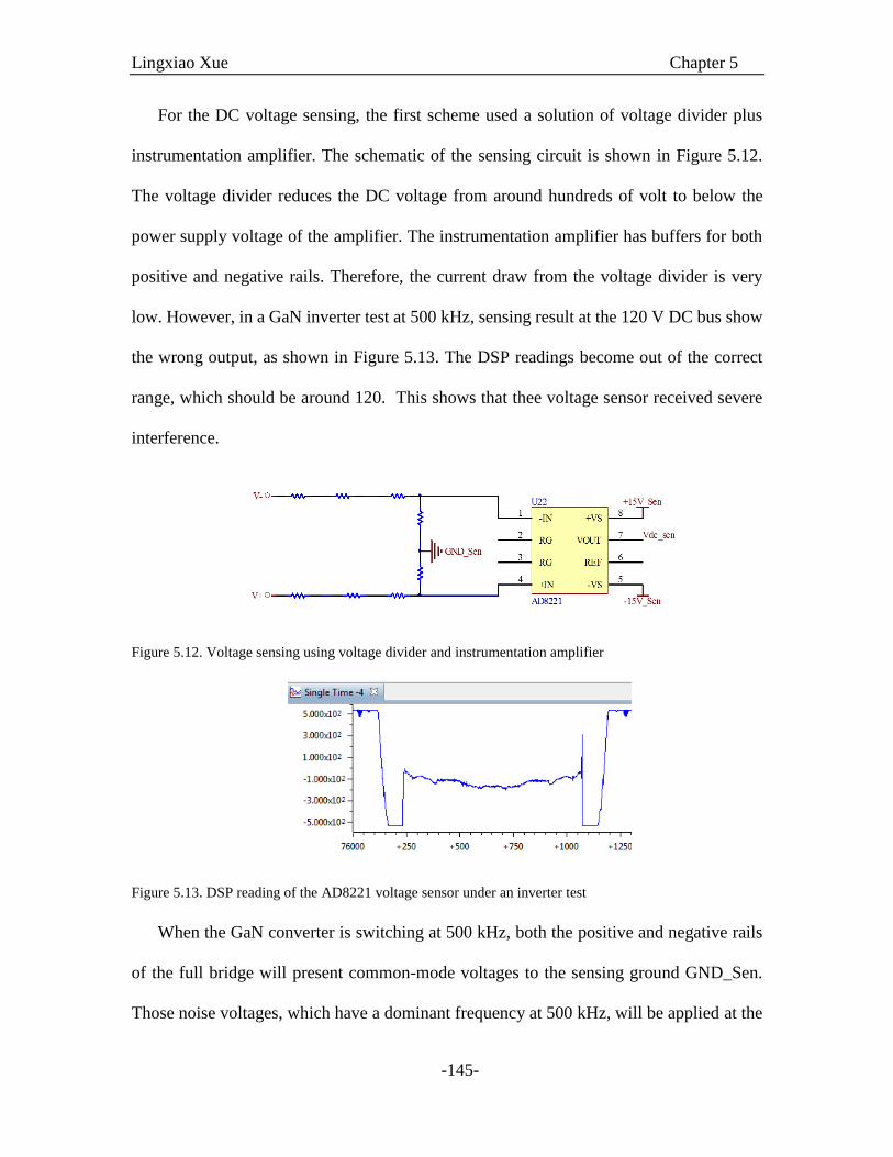
Lingxiao Xue Chapter 5
-145-
For the DC voltage sensing, the first scheme used a solution of voltage divider plus
instrumentation amplifier. The schematic of the sensing circuit is shown in Figure 5.12.
The voltage divider reduces the DC voltage from around hundreds of volt to below the
power supply voltage of the amplifier. The instrumentation amplifier has buffers for both
positive and negative rails. Therefore, the current draw from the voltage divider is very
low. However, in a GaN inverter test at 500 kHz, sensing result at the 120 V DC bus show
the wrong output, as shown in Figure 5.13. The DSP readings become out of the correct
range, which should be around 120. This shows that thee voltage sensor received severe
interference.
Figure 5.12. Voltage sensing using voltage divider and instrumentation amplifier
Figure 5.13. DSP reading of the AD8221 voltage sensor under an inverter test
When the GaN converter is switching at 500 kHz, both the positive and negative rails
of the full bridge will present common-mode voltages to the sensing ground GND_Sen.
Those noise voltages, which have a dominant frequency at 500 kHz, will be applied at the
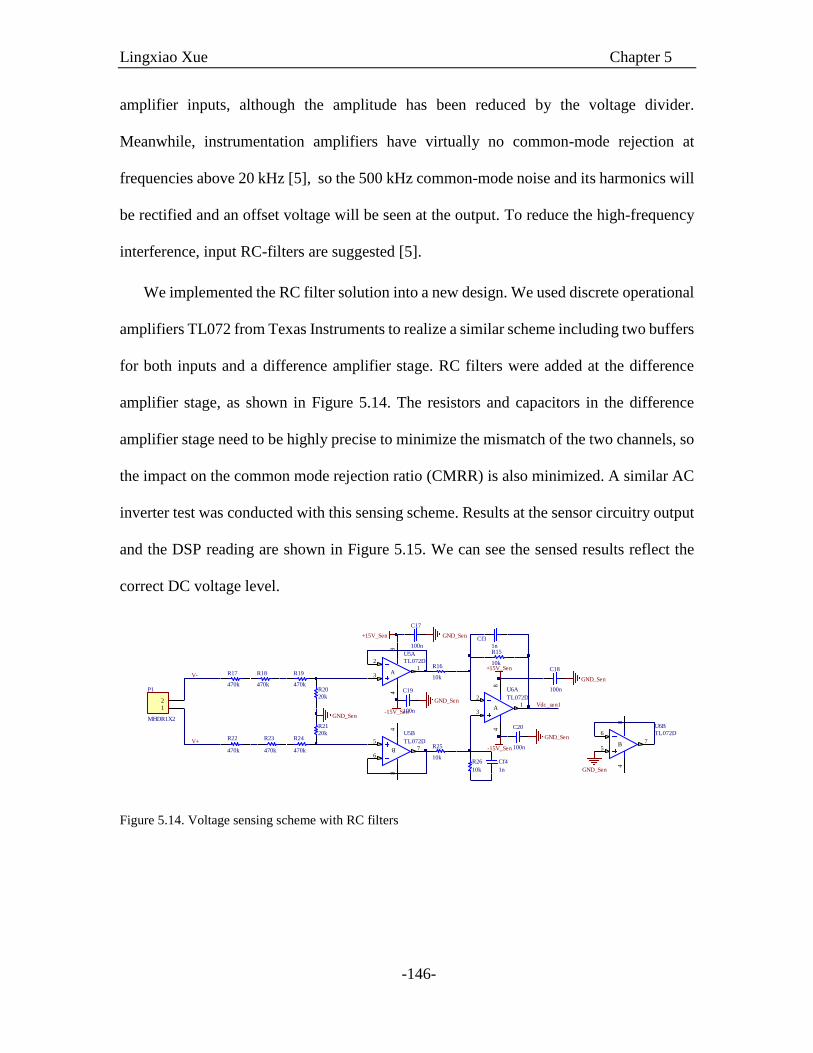
Lingxiao Xue Chapter 5
-146-
amplifier inputs, although the amplitude has been reduced by the voltage divider.
Meanwhile, instrumentation amplifiers have virtually no common-mode rejection at
frequencies above 20 kHz [5], so the 500 kHz common-mode noise and its harmonics will
be rectified and an offset voltage will be seen at the output. To reduce the high-frequency
interference, input RC-filters are suggested [5].
We implemented the RC filter solution into a new design. We used discrete operational
amplifiers TL072 from Texas Instruments to realize a similar scheme including two buffers
for both inputs and a difference amplifier stage. RC filters were added at the difference
amplifier stage, as shown in Figure 5.14. The resistors and capacitors in the difference
amplifier stage need to be highly precise to minimize the mismatch of the two channels, so
the impact on the common mode rejection ratio (CMRR) is also minimized. A similar AC
inverter test was conducted with this sensing scheme. Results at the sensor circuitry output
and the DSP reading are shown in Figure 5.15. We can see the sensed results reflect the
correct DC voltage level.
Figure 5.14. Voltage sensing scheme with RC filters
470k
R23
470k
R24
20k
R20470k
R18
470k
R19
20k
R21
GND_Sen-15V_Sen
470k
R17
470k
R22
Vdc_sen1
10k
R25
2
3
1A
84
U5A
TL072D
5
6
7B
84
U5B
TL072D
2
3
1A
84
U6A
TL072D
10k
R1610k
R15
10k
R26
+15V_Sen
-15V_Sen 5
6
7B
84
U6B
TL072D
GND_Sen
1n
Cf3
1n
Cf4
100n
C17
GND_Sen
100n
C19
GND_Sen
100n
C18
GND_Sen
100n
C20
GND_SenV+
V-
+15V_Sen
1
2
P1
MHDR1X2
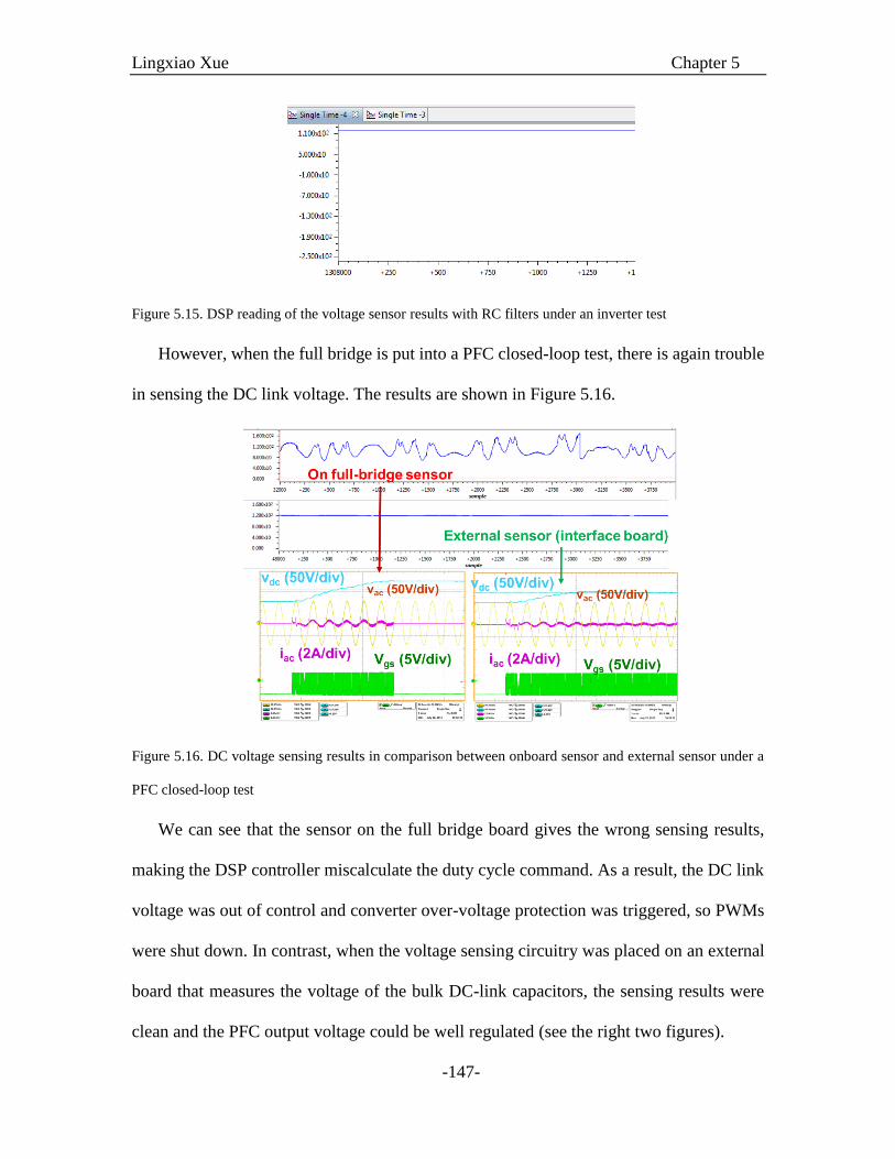
Lingxiao Xue Chapter 5
-147-
Figure 5.15. DSP reading of the voltage sensor results with RC filters under an inverter test
However, when the full bridge is put into a PFC closed-loop test, there is again trouble
in sensing the DC link voltage. The results are shown in Figure 5.16.
Figure 5.16. DC voltage sensing results in comparison between onboard sensor and external sensor under a
PFC closed-loop test
We can see that the sensor on the full bridge board gives the wrong sensing results,
making the DSP controller miscalculate the duty cycle command. As a result, the DC link
voltage was out of control and converter over-voltage protection was triggered, so PWMs
were shut down. In contrast, when the voltage sensing circuitry was placed on an external
board that measures the voltage of the bulk DC-link capacitors, the sensing results were
clean and the PFC output voltage could be well regulated (see the right two figures).
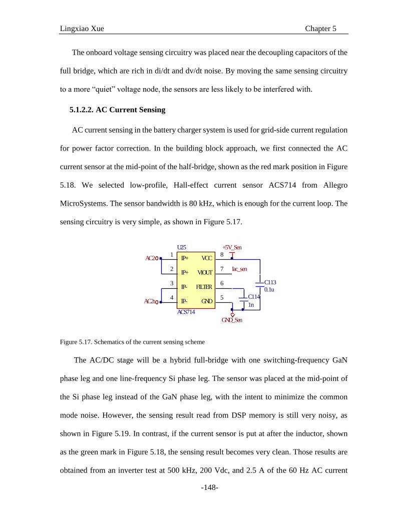
Lingxiao Xue Chapter 5
-148-
The onboard voltage sensing circuitry was placed near the decoupling capacitors of the
full bridge, which are rich in di/dt and dv/dt noise. By moving the same sensing circuitry
to a more “quiet” voltage node, the sensors are less likely to be interfered with.
5.1.2.2. AC Current Sensing
AC current sensing in the battery charger system is used for grid-side current regulation
for power factor correction. In the building block approach, we first connected the AC
current sensor at the mid-point of the half-bridge, shown as the red mark position in Figure
5.18. We selected low-profile, Hall-effect current sensor ACS714 from Allegro
MicroSystems. The sensor bandwidth is 80 kHz, which is enough for the current loop. The
sensing circuitry is very simple, as shown in Figure 5.17.
Figure 5.17. Schematics of the current sensing scheme
The AC/DC stage will be a hybrid full-bridge with one switching-frequency GaN
phase leg and one line-frequency Si phase leg. The sensor was placed at the mid-point of
the Si phase leg instead of the GaN phase leg, with the intent to minimize the common
mode noise. However, the sensing result read from DSP memory is still very noisy, as
shown in Figure 5.19. In contrast, if the current sensor is put at after the inductor, shown
as the green mark in Figure 5.18, the sensing result becomes very clean. Those results are
obtained from an inverter test at 500 kHz, 200 Vdc, and 2.5 A of the 60 Hz AC current
IP+1
IP+2
IP-3
IP-4
GND5
FILTER6
VIOUT7
VCC8
U24
ACS714
+5V_Sen
V-
V-t
GND_Sen
1n
C109
0.1u
C108
IP+1
IP+2
IP-3
IP-4
GND5
FILTER6
VIOUT7
VCC8
U25
ACS714
+5V_Sen
AC2
AC2t
GND_Sen
1n
C114
0.1u
C113
Idc_sen
Iac_sen
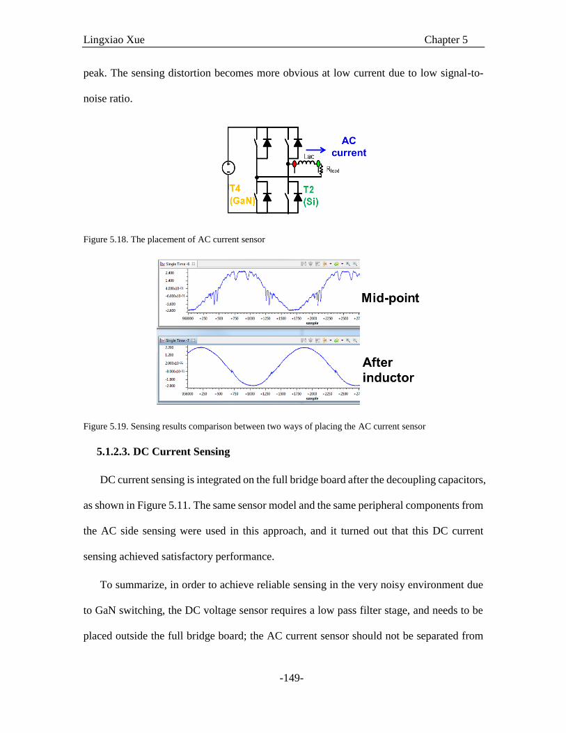
Lingxiao Xue Chapter 5
-149-
peak. The sensing distortion becomes more obvious at low current due to low signal-to-
noise ratio.
Figure 5.18. The placement of AC current sensor
Figure 5.19. Sensing results comparison between two ways of placing the AC current sensor
5.1.2.3. DC Current Sensing
DC current sensing is integrated on the full bridge board after the decoupling capacitors,
as shown in Figure 5.11. The same sensor model and the same peripheral components from
the AC side sensing were used in this approach, and it turned out that this DC current
sensing achieved satisfactory performance.
To summarize, in order to achieve reliable sensing in the very noisy environment due
to GaN switching, the DC voltage sensor requires a low pass filter stage, and needs to be
placed outside the full bridge board; the AC current sensor should not be separated from
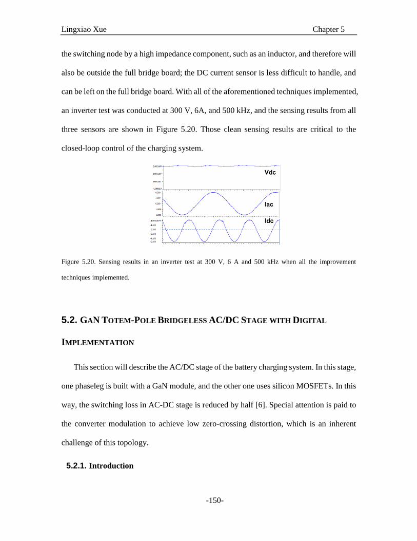
Lingxiao Xue Chapter 5
-150-
the switching node by a high impedance component, such as an inductor, and therefore will
also be outside the full bridge board; the DC current sensor is less difficult to handle, and
can be left on the full bridge board. With all of the aforementioned techniques implemented,
an inverter test was conducted at 300 V, 6A, and 500 kHz, and the sensing results from all
three sensors are shown in Figure 5.20. Those clean sensing results are critical to the
closed-loop control of the charging system.
Figure 5.20. Sensing results in an inverter test at 300 V, 6 A and 500 kHz when all the improvement
techniques implemented.
5.2. GAN TOTEM-POLE BRIDGELESS AC/DC STAGE WITH DIGITAL
IMPLEMENTATION
This section will describe the AC/DC stage of the battery charging system. In this stage,
one phaseleg is built with a GaN module, and the other one uses silicon MOSFETs. In this
way, the switching loss in AC-DC stage is reduced by half [6]. Special attention is paid to
the converter modulation to achieve low zero-crossing distortion, which is an inherent
challenge of this topology.
5.2.1. Introduction

Lingxiao Xue Chapter 5
-151-
The totem-pole PFC, belonging to the bridgeless PFC family, is able not only to reduce
conduction loss, especially at the low line, but also features low emission of common mode
EMI noise [7-9]. However, the traditional totem-pole PFC converter uses a silicon super
junction MOSFET and thus suffers from severe reverse recovery of the MOSFET body
diode when operating in continuous conduction mode (CCM). Therefore, critical-
conduction mode (CRM) is usually used to achieve zero-voltage switching or valley
switching to overcome the impact of the diode reverse-recovery and high switching loss at
turn-on [10, 11]. In addition, by replacing the two rectifier diodes with two big MOSFETs,
the resultant active H-bridge enables the converter to achieve more flexible controllability,
and in turn offers advantages such as extended ZVS range for fast switches, bi-directional
capability, and low condition loss compared to the pure diode solution [12]. Recently, GaN
HEMT has shown to be promising when implemented into this topology, even in
continuous conduction mode, due to very low reverse recovery and switching loss [6, 13].
If CRM and interleaving are used, the converter frequency can be further increased due to
less loss, and thus the passive size can be further reduced [14].
The totem-pole PFC topology has a slow commutation leg at the line frequency and a
fast commutation leg at the switching frequency. This characteristic, as will be detailed
later, actually makes the controller, modulator, and gate driver design tricky. One widely
reported issue is the current spike at the zero-crossing of AC voltage [10, 13, 15]. Contrary
to the well documented zero-crossing current distortion phenomena in [16-19], which is
mainly associated with the current controller design and discontinuous conduction mode
operation, this zero-crossing current spike relies more on the modulator, as will be detailed
in this paper. In fact, at the zero-crossing, the modulation could be so sensitive that the

Lingxiao Xue Chapter 5
-152-
modulator has to adopt soft-transition [10, 13] or be deactivated around the zero-crossing
[12]. Those methods all sacrifice the AC current controllability around the zero-crossing;
therefore, the current will be distorted to some extent, although only slightly in the
designated specifications. However, with the continued increase of the switching frequency
of the switches of the fast leg, and the desire to increase the chip area of those of the slow
leg for lower conduction loss, it can be expected that the enlarged switching speed
difference between the two legs will make the zero-crossing problem more severe. In
addition, at high switching frequency, the reduced PFC inductance will cause this situation
to deteriorate because of the larger current slew rate. Therefore, a deeper understanding
and better solution for the totem-pole bridgeless PFC at the AC voltage zero-crossing is
needed.
This section will analyze the operation of the totem-pole bridgeless PFC converter,
especially around the zero-crossing point, in detail and summarize different solutions. The
CCM control is highlighted here for simplicity, but the analysis principle can be applied to
CRM control as well. The only difference is that in CRM control, the on-time is constant,
and a different duty cycle is achieved by varying switching frequency. Different digital
implementations of modulators are tested to solve the issue of the zero-crossing spike. The
most robust modulator can be both zero-crossing spike free and current offset free.
5.2.2. Operation of Totem-Pole Bridgeless PFC
The totem-pole bridgeless PFC schematics are shown in Figure 5.21. In this
investigation, all four switches in the H-bridge are active switches. The low frequency (LF)
phase leg only commutates at line frequency, while the high frequency (HF) phase leg will

Lingxiao Xue Chapter 5
-153-
chop the DC voltage at high frequency. In this case, the low-frequency phase leg can use a
very large MOSFET, and thus the on-resistance can be very low.
Lac
vac
iac
Slf(T)
Slf(B)
Shf(T)
Shf(B)
vl
vh
Vdcvhl
+
-
Figure 5.21. Totem-pole bridgeless PFC schematic
The basic functionality of any PFC circuit is to regulate the output voltage so it is
constant and control the input current so it is sinusoidal and in phase with the input voltage,
which means they should fulfill
2 sin( )ac acv V t (5.1)
2 sin( )ac aci I t (5.2)
Then the PFC converter with a unity power factor should have the waveforms at a
fundamental frequency as shown in Figure 5.22 (a), which considers the voltage drop
across the AC inductor vL. The phasor diagram of those key voltage and current quantities
is derived in Figure 5.22 (b).

Lingxiao Xue Chapter 5
-154-
vhl
vac
iac
θ t1
(a) (b)
Figure 5.22. Fundamental frequency analysis of PFC converter under unity power factor: (a) current and
voltage waveforms at fundamental frequency; (b) phasor diagram of the current and voltage quantities
From the phasor diagram, we can determine that the required full bridge output voltage
vhl should be
2
sin( t ), tancos
ac ac achl
ac
V L Iv
V
(5.3)
Equation (5.3) shows the current control law of a single-phase PFC circuit with an AC
inductor whose current has both positive and negative polarities. If the full bridge voltage
vhl is provided exactly as shown in (5.3), the AC current becomes perfectly sinusoidal and
in phase with the AC voltage. Then the required duty cycle dhl, which is proportional to the
fundamental value of the full-bridge output voltage between the two AC nodes, vhl, should
satisfy
/hl hl dcd v V (5.4)
In the totem-pole bridgeless configuration, the slow leg commutates at line frequency;
therefore, the only possible duty cycle pattern for the two-phase legs of the full bridge in
Figure 5.21 to meet (5.3) and (5.4) should be

Lingxiao Xue Chapter 5
-155-
2sin( t ), 0
cos
21 sin( ), 0
cos
0, 0
1, 0
achl
dchh
dc achl
dc
hlll
hldc
Vif d
Vvd
V Vt if d
V
if dvd
if dV
(5.5)
2
sin( t )cos
achl h l
Vd d d
(5.6)
in which dh and dl are the duty cycles for the high-frequency phase leg and low-frequency
phase leg, respectively. Note that in (5.5) the modulator mode changes every line cycle;
this is selected with the dhl condition statement. Implementation of (5.5) enables line
frequency switching of Slf(T) and Slf(B) by commutating them only at the zero transition of
dhl in (5.6). To be clear, at the positive line cycle of dhl, Slf(B) should be on, and the circuit
will operate as a boost converter in which Shf(B) is the PWM switch and Shf(T) is the
synchronous rectifier. For the negative line cycle of dhl, Slf(T) will be on, but differing from
the positive line cycle, Shf(T) will be the Boost PWM switch, and Shf(B) becomes the
synchronous rectifier.
We should note that the modulator behavior has to change according to the polarity of
the duty cycle command dhl instead of the AC voltage as the PFC control law (5.3), which
is what most published research on totem-pole bridgeless PFC converters has suggested
using. The main difference between the two signals is a certain phase delay, which depends
on the line frequency, inductance, AC current, and AC voltage, as quantified in (5.3) . In
practice, this phase delay is usually very small in the steady state, due to high switching
frequency, low line frequency, and small AC inductance. Therefore, it is reasonable to
assume

Lingxiao Xue Chapter 5
-156-
2 sin( t)
2sin( t)
hl ac
achl
dc
v V
Vd
V
(5.7)
and then (5.4), (5.5) and (5.6) can be simplified accordingly. It is also valid that in the
condition statement of (5.5), the AC voltage can replace the duty cycle command. This
makes no obvious difference in the steady state, but will impact the converter startup
dynamics significantly, as will be discussed in the experimental section. Therefore,
generally speaking, it is still better to use the duty cycle command instead of the AC voltage
to determine the polarity of the modulator.
It is worth mentioning that during this very short phase delay, taking the θ period in
Figure 5.22(a) as an example, the top switch Slf(T) should be on, according to (5.5) while
the AC current is positive, which means the current needs to flow through the channel of
this current-bidirectional switch. In contrast, a current-unidirectional switch -- say a diode
– does not allow for conduction in the same case, and current distortion, although it might
be tiny, will occur. This is another reason that a slow leg with MOSFETs instead of a diode
is preferred.
Actually, in diode-based PFC circuits, the unidirectional conduction property
essentially prohibits current in another direction, which is theoretically required to deliver
the correct voltage in (5.3). This not only applies to the single phase PFC circuit with an
AC inductor, which is the focus of this paper, but also has validity in its DC inductor
counterparts, in which the inductor can only conduct positive current due to the diode
blocking effect [16]. The traditional boost PFC falls into this category. Some research

Lingxiao Xue Chapter 5
-157-
yielded current distortion around the zero-crossing, essentially because of unidirectional
current flow caused by using diodes in the PFC converter [19-21] [17].
In all, by using a pure active H-bridge, we can eliminate the items above caused by
unidirectional conduction, thereby theoretically achieving no current distortion around the
zero-crossing. However, the totem-pole bridgeless PFC has some inherent challenges that
need to be addressed to achieve distortion-free current at the zero-crossing. We will
examine those factors in the next section.
5.2.3. Current Spike around Zero-Crossing of AC Voltage
Figure 5.23 depicts the key waveforms at the negative-to-positive transition of AC
voltage in a unity power factor condition. Compared to Figure 5.22, the vhl waveform in
Figure 5.23(a) also contains the switching frequency component. The phase delay due to
AC inductor voltage drop is ignored in Figure 5.23(a), so the zero-crossing points of the
duty cycle command vhl and the AC voltage vac almost overlap with each other. We can
also see how the low-frequency phase leg flips polarity at the zero-crossing point in Figure
5.23(c). From (5.7), we know the full bridge should output very narrow pulses to make vhl
almost zero. Accordingly, the pulse duty cycle of the AC node voltage of the high-
frequency phase leg vh has to change abruptly from nearly 100% to 0% in Figure 5.23(d).
As long as the required pulse array is generated as Figure 5.23(a), then the inductor current
will follow the triangular wave in Figure 5.23(b) without any distortion.
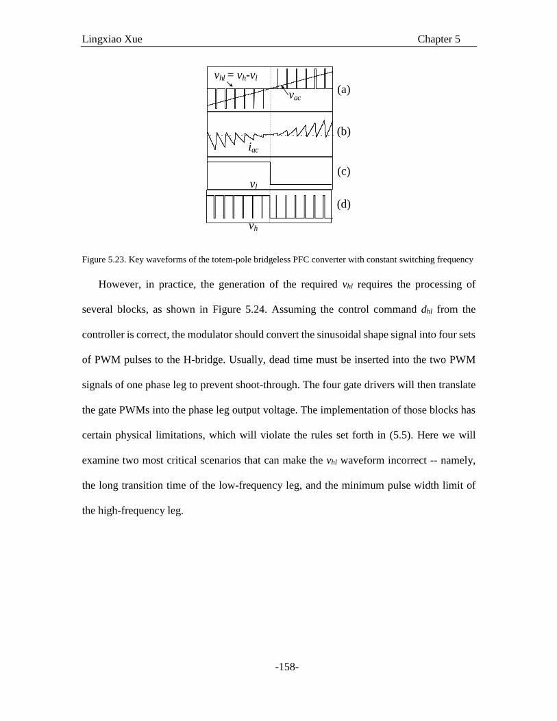
Lingxiao Xue Chapter 5
-158-
vhl = vh-vl
iac
vl
vh
vac(a)
(b)
(c)
(d)
Figure 5.23. Key waveforms of the totem-pole bridgeless PFC converter with constant switching frequency
However, in practice, the generation of the required vhl requires the processing of
several blocks, as shown in Figure 5.24. Assuming the control command dhl from the
controller is correct, the modulator should convert the sinusoidal shape signal into four sets
of PWM pulses to the H-bridge. Usually, dead time must be inserted into the two PWM
signals of one phase leg to prevent shoot-through. The four gate drivers will then translate
the gate PWMs into the phase leg output voltage. The implementation of those blocks has
certain physical limitations, which will violate the rules set forth in (5.5). Here we will
examine two most critical scenarios that can make the vhl waveform incorrect -- namely,
the long transition time of the low-frequency leg, and the minimum pulse width limit of
the high-frequency leg.
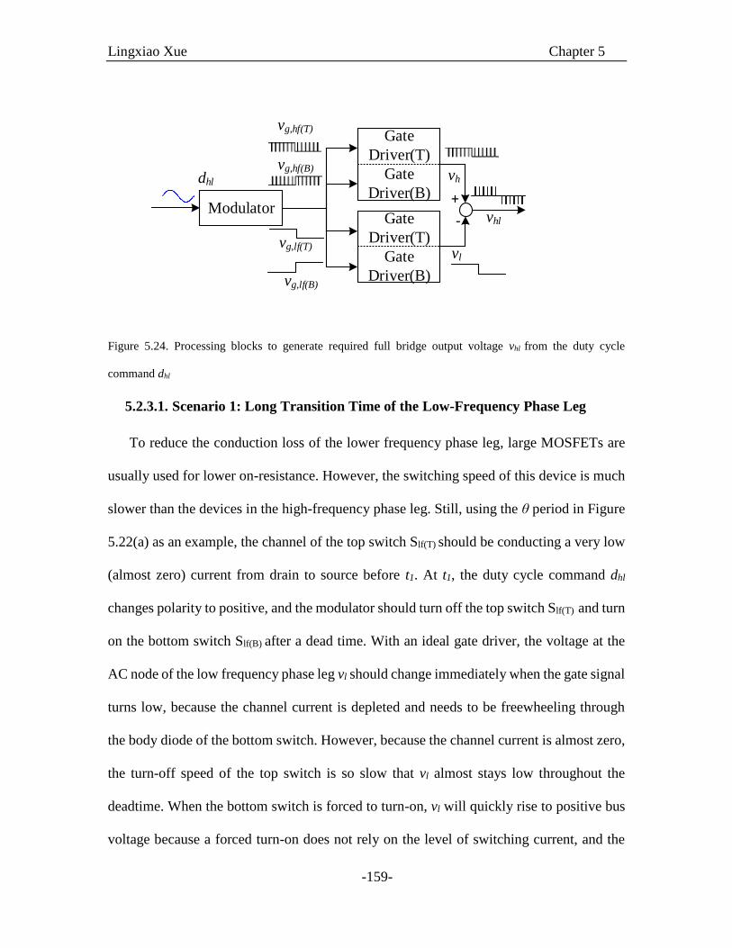
Lingxiao Xue Chapter 5
-159-
vh
Modulator+
- vhl
vl
Gate
Driver(T)
Gate
Driver(B)
Gate
Driver(T)
Gate
Driver(B)
vg,hf(T)
vg,hf(B)
vg,lf(T)
vg,lf(B)
dhl
Figure 5.24. Processing blocks to generate required full bridge output voltage vhl from the duty cycle
command dhl
5.2.3.1. Scenario 1: Long Transition Time of the Low-Frequency Phase Leg
To reduce the conduction loss of the lower frequency phase leg, large MOSFETs are
usually used for lower on-resistance. However, the switching speed of this device is much
slower than the devices in the high-frequency phase leg. Still, using the θ period in Figure
5.22(a) as an example, the channel of the top switch Slf(T) should be conducting a very low
(almost zero) current from drain to source before t1. At t1, the duty cycle command dhl
changes polarity to positive, and the modulator should turn off the top switch Slf(T) and turn
on the bottom switch Slf(B) after a dead time. With an ideal gate driver, the voltage at the
AC node of the low frequency phase leg vl should change immediately when the gate signal
turns low, because the channel current is depleted and needs to be freewheeling through
the body diode of the bottom switch. However, because the channel current is almost zero,
the turn-off speed of the top switch is so slow that vl almost stays low throughout the
deadtime. When the bottom switch is forced to turn-on, vl will quickly rise to positive bus
voltage because a forced turn-on does not rely on the level of switching current, and the
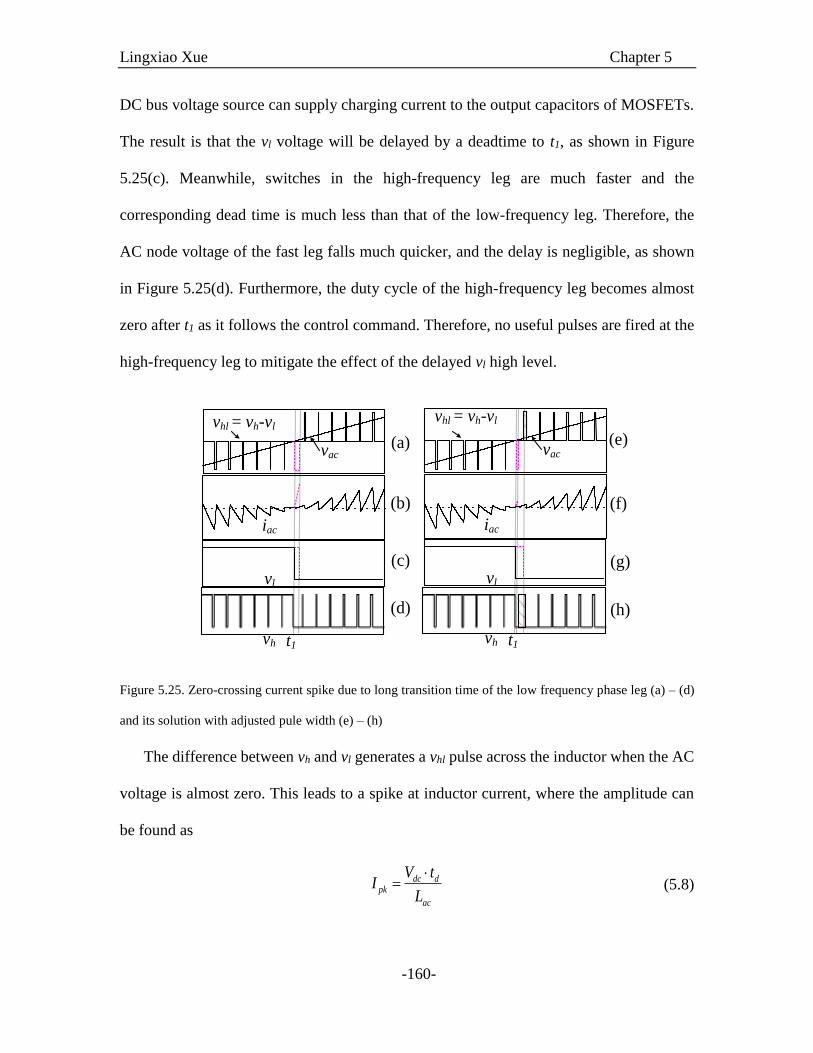
Lingxiao Xue Chapter 5
-160-
DC bus voltage source can supply charging current to the output capacitors of MOSFETs.
The result is that the vl voltage will be delayed by a deadtime to t1, as shown in Figure
5.25(c). Meanwhile, switches in the high-frequency leg are much faster and the
corresponding dead time is much less than that of the low-frequency leg. Therefore, the
AC node voltage of the fast leg falls much quicker, and the delay is negligible, as shown
in Figure 5.25(d). Furthermore, the duty cycle of the high-frequency leg becomes almost
zero after t1 as it follows the control command. Therefore, no useful pulses are fired at the
high-frequency leg to mitigate the effect of the delayed vl high level.
vhl = vh-vl
iac
vl
vh
vac
(e)
(f)
(g)
(h)
t1
vhl = vh-vl
iac
vl
vh
vac(a)
(b)
(c)
(d)
t1
Figure 5.25. Zero-crossing current spike due to long transition time of the low frequency phase leg (a) – (d)
and its solution with adjusted pule width (e) – (h)
The difference between vh and vl generates a vhl pulse across the inductor when the AC
voltage is almost zero. This leads to a spike at inductor current, where the amplitude can
be found as
dc d
pk
ac
V tI
L
(5.8)

Lingxiao Xue Chapter 5
-161-
For a 400 V bus system and 500 ns deadtime with a 100 µH inductor, the resultant
current spike is 2 A. If a much smaller inductance is used — for example, that in an
interleaved critical conduction mode PFC — the current spike will scale up proportionally.
This scenario can be summarized as misalignment of the voltage transition edges
between the low-frequency leg and the high-frequency leg. This phenomenon is also shown
in [10, 13], in which a similar transition delay was also observed. In [10], the low-frequency
leg consists of two large diodes, so the transition delay is rooted in diode reverse recovery.
In [13], the modulator turns off the two MOSFETs for a short blanking or “soft-start”
period, so the totem-pole bridgeless collapses to the diode version around zero crossing.
As a result, natural diode reverse recovery will occur and cause voltage transition delay at
the zero-crossing. Both papers addressed this zero-crossing issue by adjusting the pulse
width of the high-frequency leg node voltage. As shown in Figure 5.25 (h), instead of an
almost 0% duty cycle, a wider pulse width will help to cancel the effect of the transition
delay from the low frequency leg, reducing the current spike (c.f. Figure 5.25 (f)). In the
implementations, reference [10] limited the on-time of the PWM switch in constant-on
time control, and reference [13] made a soft transition of duty cycle from 100% to 0%
around the zero-crossing. Since diode leg commutation might be very slow and last several
switching cycles, the scheme in Figure 5.25 (h) needs to be implemented throughout those
switching cycles accordingly.
5.2.3.2. Scenario 2: Minimum Pulse Width of the High-Frequency Phase Leg
In scenario 1, we see how the transition delay of the AC node voltage of the low
frequency leg can generate a high current spike, with the joint contribution of the almost
zero duty cycle of the AC node voltage of the high frequency leg. However, the high-

Lingxiao Xue Chapter 5
-162-
frequency leg, with such an extreme pulse duty cycle, has additional problems. Around the
zero-crossing, the required duty cycle for the switches in the high-frequency leg lies in the
vicinity of 100% and 0%. When the duty cycle is too small, any pulses shorter than the
deadtime will be blanked, resulting in a low driving level. Similarly, an almost full duty
cycle will output a high driving level under the impact of deadtime. Even when some
narrow (or over long) pulses can survive the deadtime generating circuit, the resultant
drain-to-source voltage cannot follow the PWM gate signals because of the finite transition
slew rate. In other words, with narrow pulses, the device cannot be fully turned-on, while
with pulses that are too long, the device cannot be fully turned off. As a result, at the zero-
crossing, some very narrow (or long) pulses of the AC node voltage at the high frequency
leg vh will be blanked and show low (or high) levels, as illustrated in Figure 5.26(d).
vhl = vh-vl
iac
vl
vac
(a)
(b)
(c)
(d)
t1 =0t2 t3
vh
Figure 5.26. Zero-crossing current spike due to minimum pulse width of the high-frequency leg
During the blanking interval (t0 - t2), only the AC voltage will be applied across the AC
inductor Lac. Assuming the minimum duty cycle dhl that can be sent without blanking effect
is Dm, the instant t2 where blanking starts to appear in a line cycle should fulfill (5.9) when
considering (5.7)

Lingxiao Xue Chapter 5
-163-
2
2sin( )ac
m
dc
VD t
V (5.9)
in which we define the zero time at t1, so t2 is negative. Then from t2 to t3, the inductor
current depends on the applied AC voltage and its initial condition at t2. By ignoring the
switching ripple, the inductor current can be derived as
2
2 2 3
2 (cos( ) cos( ))( )
2 sin( )
acac
ac
ac
V t ti t
L
I t t t t
(5.10)
The peak current appears at t = t1 = 0, where the AC voltage crosses zero. Substituting
this in (5.10) yields
22
2 (1 cos( ))2 sin( )ac
pk ac
ac
V tI I t
L
(5.11)
(5.9) and (5.11) can determine the peak current. Considering the following
specifications: Vac = 150 V, Vdc = 250 V, Iac = 6.7 A, Lac = 100 µH, and switching frequency
at 500 kHz, and a minimum duty cycle 0.025, the calculated current spike will be -2.72 A.
In fact, since the interval between t2 to t3 can last many switching cycles – 38 switching
cycles in the previous example – the controller will take over and interfere with this passive
excitation process. Figure 5.27 shows the simulation results of a totem-pole PFC converter
with a minimum duty cycle of ±0.025. In the simulation, we use ideal switches, so the gate
drive signals directly swing the drain-to-source voltages. When the duty cycle command
drops into the minimum duty cycle band (-0.025, 0.025), the modulator will give either low
or high driving levels, depending on the duty cycle command polarity, as shown in Figure

Lingxiao Xue Chapter 5
-164-
5.27(b) and Figure 5.27(c). This also means the current controller cannot force the inductor
current to track the current reference any longer within this band.
-2
0
2
-0.05
0.00
0.05
× 1e-11.165 1.166 1.167 1.168 1.169
0.0
250
vh
dhl0.025
-0.025
vac(a)
(b)
(c)
t1 t2 t3t'1
iac
Figure 5.27. Simulation results of zero-crossing current spike due to long transition time of the low frequency
phase leg
We can see that the current dropping, which starts from t2, does not follow the predicted
dashed line indicated by (5.10) in Figure 5.27(a). Instead, it reverses direction before it
reaches the AC voltage zero-crossing point at t1. The reason is that the control command
dhl leaves the minimum duty cycle band so that the gate drives fire several pulses to correct
the inductor current to the nearly-zero current reference, until the control command enters
the band again. Within the band, the inductor current responds to the AC voltage excitation
in a sinusoidal shape. At t3, the duty cycle command becomes higher than the positive limit
of the band, and thus the controller resumes regulating the current.
It is worth mentioning that due to the influence of the current controller, the
inductor current does not drop to the negative minimum Ipk as predicted in (5.11) , but rises
to another positive peak at t3. This peak still has a smaller magnitude compared to Ipk

Lingxiao Xue Chapter 5
-165-
because from t1 to t3 in Figure 5.27 (a), both current curves (solid and dashed) are changing
with the same slew rate due to the same voltage excitation. However, the solid curve
obviously starts with a lower negative value than Ipk., The controller suffers from dynamics
with the minimum-duty-cycle band, as shown in Figure 5.27 (b), which makes the control
command (solid line) deviate from the steady state value in (5.7) (dashed line). The
dynamic adjustment of the current controller causes additional current overshoot after t3,
as can be seen in Figure 5.27 (a).
5.2.4. Digital Implementation of Modulator
In the previous section, we summarized two mechanisms that can cause a zero-crossing
current spike. Both mechanisms result from using a modulator and gate drivers. As gate
driver designs are mainly determined by the power semiconductor devices, and can never
be ideal, a reasonable solution should focus on the improvement of the modulator. As we
will see in this section, a good modulator design can alleviate the effects of transition delay
of the low-frequency leg and the minimum pulse limit of the high-frequency leg. We will
first introduce the basic realization of a digital modulator, and then show the methods of
improvement used to solve the two zero-crossing issues.
5.2.4.1. Basic DSP-based Digital Modulator Implementation for Totem-Pole
Bridgeless PFC
In this work, the modulator is realized using the ePWM module of the Texas Instrument
TMS320C28343 DSP processor [22]. The ePWM module is a counter-based module. The
most critical block diagram of the implementation is shown in Figure 5.28.
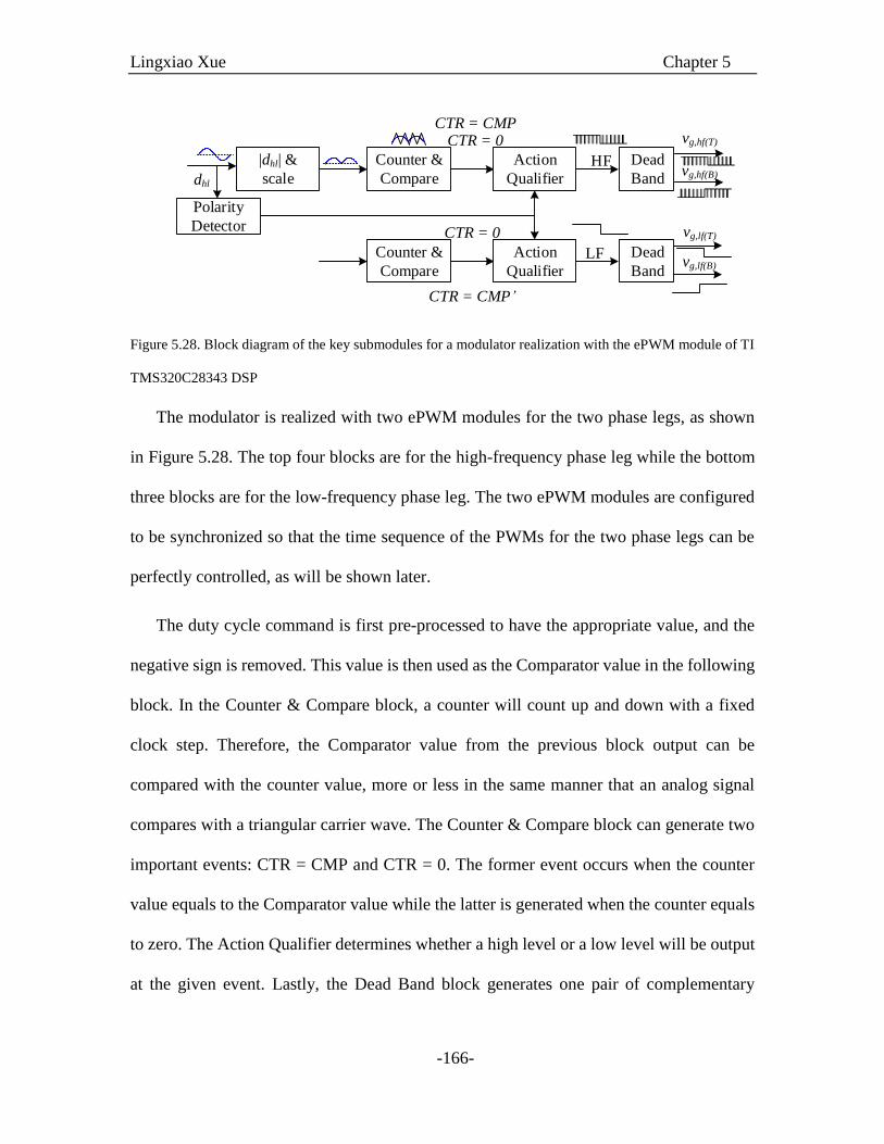
Lingxiao Xue Chapter 5
-166-
vg,hf(T)
vg,hf(B)
vg,lf(T)
vg,lf(B)
dhl
Counter &
Compare
Polarity
Detector
Action
Qualifier
Dead
Band
Counter &
Compare
Action
Qualifier
Dead
Band
|dhl| &
scale
CTR = 0CTR = CMP
CTR = 0
CTR = CMP
HF
LF
Figure 5.28. Block diagram of the key submodules for a modulator realization with the ePWM module of TI
TMS320C28343 DSP
The modulator is realized with two ePWM modules for the two phase legs, as shown
in Figure 5.28. The top four blocks are for the high-frequency phase leg while the bottom
three blocks are for the low-frequency phase leg. The two ePWM modules are configured
to be synchronized so that the time sequence of the PWMs for the two phase legs can be
perfectly controlled, as will be shown later.
The duty cycle command is first pre-processed to have the appropriate value, and the
negative sign is removed. This value is then used as the Comparator value in the following
block. In the Counter & Compare block, a counter will count up and down with a fixed
clock step. Therefore, the Comparator value from the previous block output can be
compared with the counter value, more or less in the same manner that an analog signal
compares with a triangular carrier wave. The Counter & Compare block can generate two
important events: CTR = CMP and CTR = 0. The former event occurs when the counter
value equals to the Comparator value while the latter is generated when the counter equals
to zero. The Action Qualifier determines whether a high level or a low level will be output
at the given event. Lastly, the Dead Band block generates one pair of complementary

Lingxiao Xue Chapter 5
-167-
PWMs with a programmable dead time. The polarity detector will help to switch between
the two types of Action Qualifier configurations so that (5.5) can be realized.
Fig. 9 shows the operation of the modulator around the zero-crossing. It can be seen
that with the same comparator value (CMP), the output PWM signals differ depending on
the command-signal polarity. This is achieved by modifying the action qualifier.
CTRCMP
HF
LF
dhl < 0 dhl > 0
Zero-
CrossingPRD
iac
Figure 5.29. Modulator waveforms around the zero-crossing including counter waveform (CTR) and action
qualifier outputs for both high-frequency leg (HF) and low-frequency leg (LF)
In both cases, the comparator value is designed as
(1 )hlCMP d PRD (5.12)
To fulfill the duty cycle requirement in (5.5) , the action qualifier has to be set up in
this way that
1 , 00, 0
,1, 0
, 0
hlhl
HF LF
hlhl
CMPif d
if dPRDd d
CMP if dif d
PRD
(5.13)
Note that dHF = dh and dLF = dl if deadtime is ignored. Then the resultant action qualifier
operation is summarized in Table 5.1.
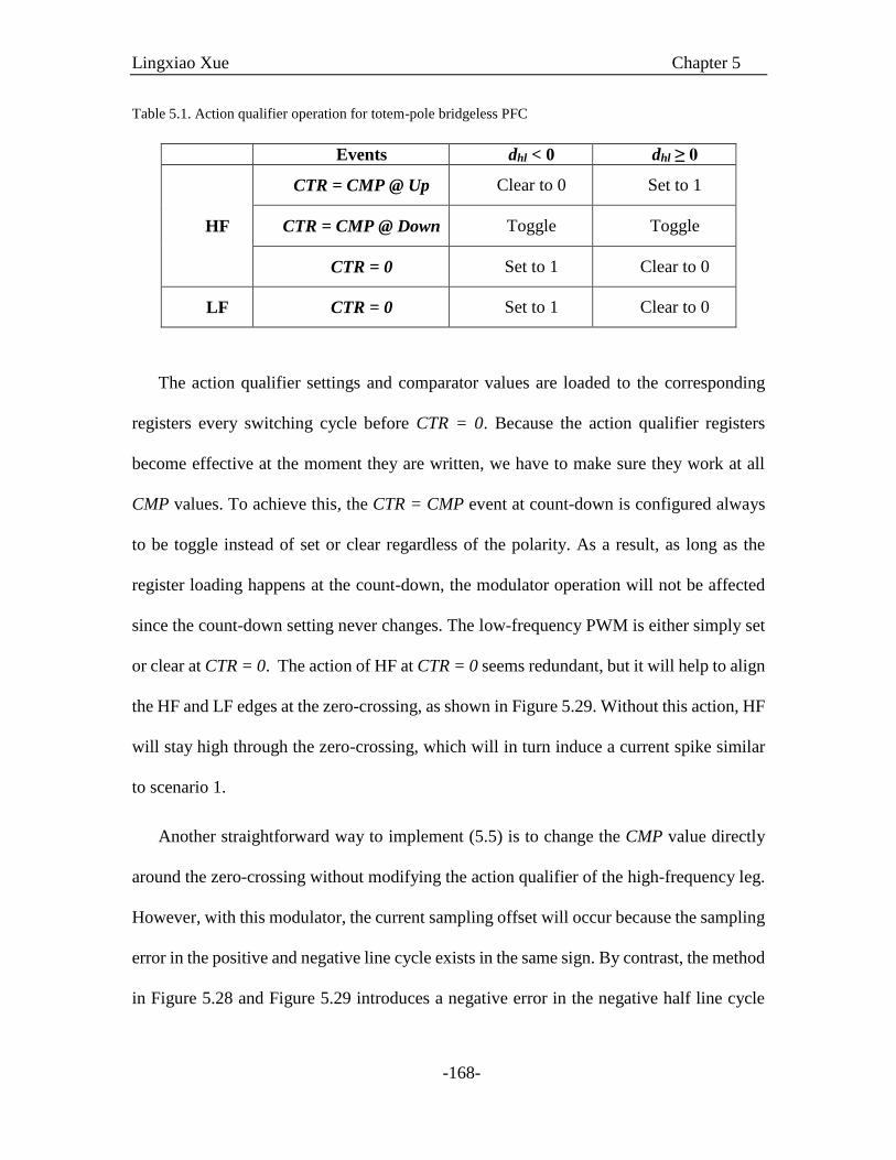
Lingxiao Xue Chapter 5
-168-
Table 5.1. Action qualifier operation for totem-pole bridgeless PFC
Events dhl < 0 dhl ≥ 0
HF
CTR = CMP @ Up Clear to 0 Set to 1
CTR = CMP @ Down Toggle Toggle
CTR = 0 Set to 1 Clear to 0
LF CTR = 0 Set to 1 Clear to 0
The action qualifier settings and comparator values are loaded to the corresponding
registers every switching cycle before CTR = 0. Because the action qualifier registers
become effective at the moment they are written, we have to make sure they work at all
CMP values. To achieve this, the CTR = CMP event at count-down is configured always
to be toggle instead of set or clear regardless of the polarity. As a result, as long as the
register loading happens at the count-down, the modulator operation will not be affected
since the count-down setting never changes. The low-frequency PWM is either simply set
or clear at CTR = 0. The action of HF at CTR = 0 seems redundant, but it will help to align
the HF and LF edges at the zero-crossing, as shown in Figure 5.29. Without this action, HF
will stay high through the zero-crossing, which will in turn induce a current spike similar
to scenario 1.
Another straightforward way to implement (5.5) is to change the CMP value directly
around the zero-crossing without modifying the action qualifier of the high-frequency leg.
However, with this modulator, the current sampling offset will occur because the sampling
error in the positive and negative line cycle exists in the same sign. By contrast, the method
in Figure 5.28 and Figure 5.29 introduces a negative error in the negative half line cycle

Lingxiao Xue Chapter 5
-169-
and a positive error in the positive line cycle. As a result, through the entire line cycle, the
errors tend to cancel each other, as shown in the iac waveform in Figure 5.29.
5.2.4.2. Lead Time of Low-Frequency Leg to Address Zero-Crossing Spike of
Scenario 1
With the modulator scheme mentioned above, the compensation on the transition delay
of the slow phase leg is very convenient. In Figure 5.28, instead of using CTR = 0, we use
CTR = CMP’, down as the event to trigger the action qualifier. By assigning a different
value to this comparator, the lead time can be controlled. For a pure active H-bridge totem-
pole bridgeless PFC, the transition delay is mostly contributed to by the deadtime between
the complementary PWM signals. This deadtime is generated by the dead band block of
the modulator. We can therefore easily assign the applied dead band value DB to the
comparator. Please note that this comparator value is unrelated to the comparator of the
high-frequency leg. The updated action qualifier operation is summarized in Table 5.2..
Table 5.2. Action qualifier operation for totem-pole bridgeless PFC with lead time of low-frequency leg
Events dhl < 0 dhl ≥ 0
HF
CTR = CMP @ Up Clear to 0 Set to 1
CTR = CMP @ Down Toggle Toggle
CTR = 0 Set to 1 Clear to 0
LF CTR = CMP’ Set to 1 Clear to 0
5.2.4.3. DIGITAL Dithering of High-Frequency Leg Duty Cycle to Address Zero-
Crossing Spike OF SCENARIO 2
The minimum pulse width limit is limited by deadtime and gate drivers and, therefore,
is difficult to further reduce. The concept of digital dithering on the duty cycle is shown in
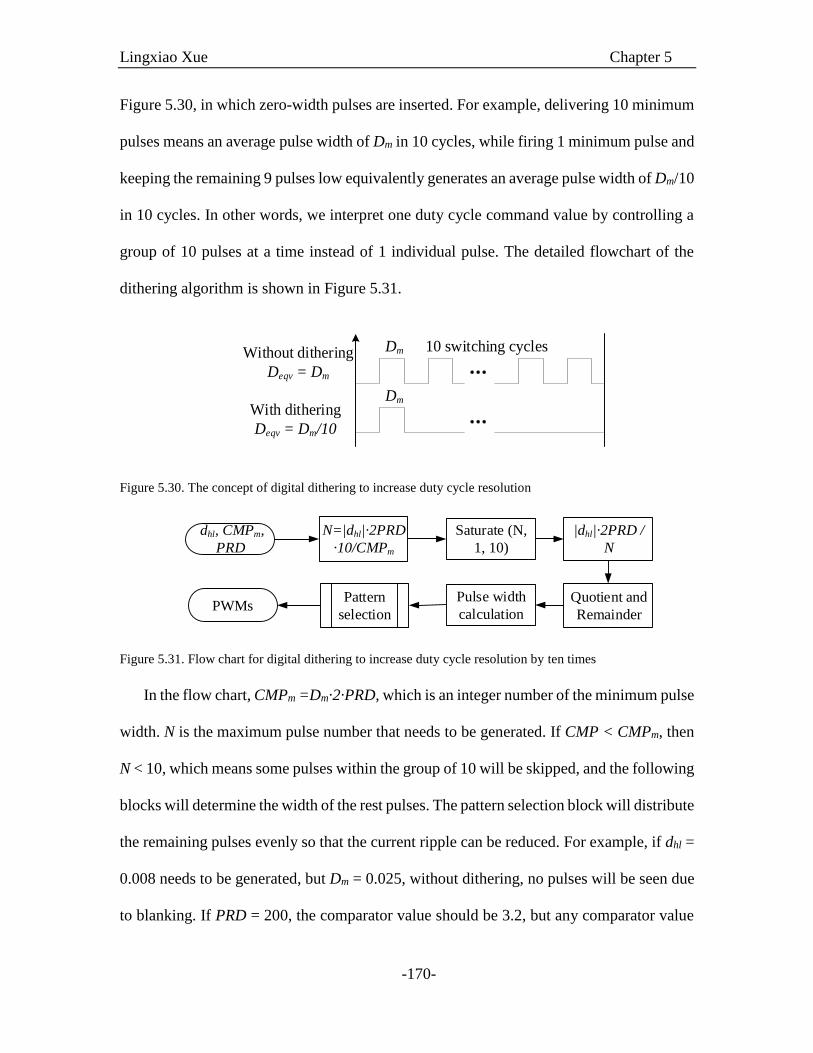
Lingxiao Xue Chapter 5
-170-
Figure 5.30, in which zero-width pulses are inserted. For example, delivering 10 minimum
pulses means an average pulse width of Dm in 10 cycles, while firing 1 minimum pulse and
keeping the remaining 9 pulses low equivalently generates an average pulse width of Dm/10
in 10 cycles. In other words, we interpret one duty cycle command value by controlling a
group of 10 pulses at a time instead of 1 individual pulse. The detailed flowchart of the
dithering algorithm is shown in Figure 5.31.
DmWithout dithering
Deqv = Dm
With dithering
Deqv = Dm/10
Dm
10 switching cycles
Figure 5.30. The concept of digital dithering to increase duty cycle resolution
dhl, CMPm,
PRD
N=|dhl|·2PRD
·10/CMPm
Saturate (N,
1, 10)
|dhl|·2PRD /
N
Quotient and
Remainder
Pattern
selectionPWMs
Pulse width
calculation
Figure 5.31. Flow chart for digital dithering to increase duty cycle resolution by ten times
In the flow chart, CMPm =Dm·2·PRD, which is an integer number of the minimum pulse
width. N is the maximum pulse number that needs to be generated. If CMP < CMPm, then
N < 10, which means some pulses within the group of 10 will be skipped, and the following
blocks will determine the width of the rest pulses. The pattern selection block will distribute
the remaining pulses evenly so that the current ripple can be reduced. For example, if dhl =
0.008 needs to be generated, but Dm = 0.025, without dithering, no pulses will be seen due
to blanking. If PRD = 200, the comparator value should be 3.2, but any comparator value

Lingxiao Xue Chapter 5
-171-
lower than ten will be blanked due to Dm = 0.025. With the dithering scheme, there will be
N = 3 pulses to generate a total width of 32 (in counter scale) within 10 switching cycles.
The pulse width calculator will generate two 11-width pulses and one 10-width pulse, and
the pattern selection block will distribute those three pulses evenly in the ten cycle group,
such as 2nd, 5th and 8th.
5.2.5. Experimental Results
A totem-pole bridgeless PFC converter is built with one GaN multi-chip half-bridge
module from HRL Laboratories and two STY139N65M514 mΩ Si MOSFETs. The
switching frequency of the GaN phase leg is at 500 kHz, and the control/sampling
frequency is 50 kHz. Therefore, the duty cycle command will be calculated every 20 µs,
and will generate ten sets of configurations for the comparator and action qualifier to
achieve dithering. Those configuration values will be loaded into the corresponding
registers every switching cycle by an interrupt with the highest priority. The control
platform is based on a Delfino C28343 DSP control card from Texas Instruments.
Figure 5.32 shows the measurement results of a converter start-up with different
modulator selection criteria. Figure 5.32 (a) uses the polarity of the duty cycle command
to change the action qualifier of the modulator, while, in Figure 5.32 (b), AC voltage
polarity is used. The PFC converter is started at around the zero crossing of the AC voltage
to avoid current reference step. We can see from Figure 5.32 (a) that the low-frequency leg
voltage has two pulses as a sign of control command polarity change to overcome the
controller dynamics. However, in Figure 5.32 (b), since the AC voltage is positive, the slow
leg voltage is always low, and so the H-bridge cannot generate the required negative vhl
pulses. As a result, the inductor current continues to drop until over-current protection is

Lingxiao Xue Chapter 5
-172-
triggered at tp. Therefore, using the polarity of the duty cycle command to select the
modulator mode gives a better dynamic performance.
Figure 5.32. Measurement start-up waveforms with different modulator selection criteria: (a) duty cycle
command dhl; (b) AC voltage vac
Figure 5.33(a) shows the measurement waveforms of the current spike at the zero-
crossing due to slow voltage transition of the low-frequency leg. From the zoom-in view
of Figure 5.33 (b), we can see that the low-frequency leg voltage vl lags the high-frequency
leg voltage vh by a 500 ns deadtime, leading to an inductor current spike. The vl voltage
edge aligns with the turn-on edge of the bottom Si switch gate voltage instead of the turn-
off edge of the top Si switch gate voltage (500 ns ahead aligned with the vh but not shown
due to lack of sufficient channels). This verifies the impact of deadtime on the low-
frequency leg. Therefore, a 500 ns lead time is programmed in the comparator of the ePWM
module of the low-frequency leg to make its PWM signals flip 500 ns earlier than the high-
frequency leg. The experimental results are shown in Figure 5.34. We can see the transition
delay is successfully compensated for (Figure 5.34 (b)) so no current spike is observed in

Lingxiao Xue Chapter 5
-173-
Figure 5.34 (a). In both Figure 5.33 and Figure 5.34, digital dithering has already been
implemented to isolate the phenomena.
Figure 5.33. Measurement waveforms of zero-crossing current spike caused by transition delay of the low-
frequency leg (scenario 1); (b) is the zoom-in waveform of (a) at zero-crossing.
Figure 5.34. Measurement waveforms after implement lead time to compensate the slow voltage transition
of the low-frequency leg (scenario 1); (b) is the zoom-in waveform of (a) at zero-crossing.
Figure 5.35 shows the measurement waveforms of the current spike at the zero-crossing
due to minimum pulse width limits. We can see around the zero-crossing that the high-
frequency leg voltage vh cannot fully swing to zero or DC rail voltages will lead to current
spike. In contrast, with digital dithering as shown in Figure 5.36, all the planned pulses are

Lingxiao Xue Chapter 5
-174-
generated, resulting in a much lower current spike. Note that at the zero-crossing, some
pulses are skipped to achieve a smaller average pulse width every ten cycles. The closer to
the zero-crossing, the more pulses are ignored.
Figure 5.35. Measurement waveforms of zero-crossing current spike caused by minimum pulse width limits
of high-frequency leg (scenario 2); (b) is the zoom-in waveform of (a) at zero-crossing
Figure 5.36. Measurement waveforms after implementing digital dithering to improve the equivalent PWM
resolution; (b) is the zoom-in waveform of (a) at zero-crossing.
Lingxiao Xue Chapter 5
-175-
5.2.6. Conclusion
The totem-pole bridgeless PFC converter is promising for the application of GaN
devices. However, inherent challenges exist for this topology at the zero-crossing point of
AC voltage. Significantly different switching speeds of power devices exist from the high-
frequency phase leg and the low-frequency leg -- almost 100% and 0% duty cycle, which
abruptly changes around the zero-crossing. As a result, a current spike is usually observed
at the zero-crossing. This phenomenon becomes more severe with wide bandgap devices
at higher switching frequencies with enlarged switching speed differences between two
legs and reduced AC inductance values. This paper provided a detailed analysis of the zero-
crossing issue in two scenarios: transition delay of the low-frequency leg and minimum
pulse width limit of the high-frequency leg. A DSP-based digital modulator was designed
to address these two issues by applying lead time to the low-frequency leg and digital
dithering to increase equivalent resolution at the high-frequency leg. Some other rules were
also summarized to enable a robust modulator design, which is the main challenge of this
topology. Experimental results, based on a 500 kHz GaN converter operating in continuous
conduction mode, verified those methods. It was also noted that using the duty cycle
command instead of AC voltage to select the modulator mode resulted in better dynamic
performance. All these findings will aid in the implementation of wide band gap devices
in very high-frequency PFC circuits.
5.3. GAN DUAL ACTIVE BRIDGE CONVERTER ANALYSIS
In Chapter 4, we introduced the control scheme of sinusoidal charging based on the
dual active bridge topology. This chapter will describe the operation of this topology at
wide load and voltage conditions, as a battery charger requires. Since the load current could

Lingxiao Xue Chapter 5
-176-
be as low as zero in the adopted sinusoidal-charging scheme, special emphasis will be
placed on the case of low load current, in which zero-voltage-switching is lost, and hard-
switching and partial zero-voltage-switching will generally happen. How to accurately
identify those different regions is important to the converter design and optimization. This
process turns out to be challenging because the phase shift value becomes comparable to
the deadtime of the two switches in a phase leg so that the classical governing equations of
DAB in [23] become inaccurate. Also, with such low phase shift, the impact of the resonant
transition between the DAB commutation inductor and the switch output capacitance is not
negligible.
Therefore, a derivation of DAB operating principle will be conducted to account for
the wide load voltage range and the extremely wide current range, including the
considerations of deadtime, resonant transition, and soft-switching and hard-switching
boundaries.
5.3.1. Dual Active Bridge Operating Principle
The DAB topology is redrawn in Figure 5.37 with the device parasitic capacitors. The
enhancement-mode GaN transistors have no body diodes, so they are not drawn in the
figure. The AC/DC stage is ignored and the input and output voltages of the DAB converter
are Vdc and Vb, respectively.
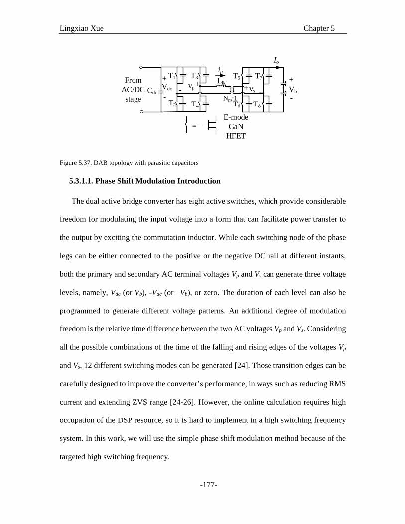
Lingxiao Xue Chapter 5
-177-
Cdc
+
-
Vdc
Nps:1
Llk +
-Vb
=
T1
T2
T3
T4
T5
T6
T7
T8
+-
vp + -vs
Io
E-mode
GaN
HFET
From
AC/DC
stage
ip
Figure 5.37. DAB topology with parasitic capacitors
5.3.1.1. Phase Shift Modulation Introduction
The dual active bridge converter has eight active switches, which provide considerable
freedom for modulating the input voltage into a form that can facilitate power transfer to
the output by exciting the commutation inductor. While each switching node of the phase
legs can be either connected to the positive or the negative DC rail at different instants,
both the primary and secondary AC terminal voltages Vp and Vs can generate three voltage
levels, namely, Vdc (or Vb), -Vdc (or –Vb), or zero. The duration of each level can also be
programmed to generate different voltage patterns. An additional degree of modulation
freedom is the relative time difference between the two AC voltages Vp and Vs. Considering
all the possible combinations of the time of the falling and rising edges of the voltages Vp
and Vs, 12 different switching modes can be generated [24]. Those transition edges can be
carefully designed to improve the converter’s performance, in ways such as reducing RMS
current and extending ZVS range [24-26]. However, the online calculation requires high
occupation of the DSP resource, so it is hard to implement in a high switching frequency
system. In this work, we will use the simple phase shift modulation method because of the
targeted high switching frequency.

Lingxiao Xue Chapter 5
-178-
With phase shift modulation, each device is driven with a 50% duty cycle and the two-
phase legs at the same side have a 180-degree phase shift, so that both of the full bridge
output voltages (Vp and Vs) are 50% of the duty cycle square wave, as shown in Figure 5.38.
When there is a phase shift φ1 between Vp and Vs, the inductor current ip will rise and fall
according to the sum of the input and output DC voltages during this phase shift interval.
In this figure, the special case in which input and output voltages satisfy Vdc = NpsVb is
taken for a conceptual demonstration. Therefore, the inductor current will stay flat when
Vp and Vs, have the same signs. Accordingly, the DAB output current will be a rectified
waveform whose transition edges align with the secondary AC terminal voltage Vs, and its
mean value is determined by the shaded area. The transition parts of the current essentially
average zero, so they do not contribute to power delivery but create the circulating energy
that is critical to realize zero-voltage switching. When the phase shift values increase from
φ1 to φ2, the shaded region also increases its area, thereby delivering more output current.
However, when further increasing the phase shift, the shaded area reduces, which means
that the average output current drops. In the next step, we will derive the exact analytical
expression for the power transfer.

Lingxiao Xue Chapter 5
-179-
0
φ1
π
ip
t
vp
vs
io
t0
io
t1
Figure 5.38. The concept of DAB power transfer
5.3.1.2. Power Delivery under Phase Shift Modulation
The power delivery equations can be found in various papers [23, 27], and will be only
briefly repeated here. A more generic DAB example is shown in Figure 5.39.
π
ip
t
vp
vs
φ
t1t0
Ip(sw)
Is(sw)
vdc
vb
Ts/2
φ
-Is(sw)
-Ip(sw)
Figure 5.39. Ideal DAB waveforms ignoring deadtime and parasitic capacitances
From t0 to t1, the inductor current is

Lingxiao Xue Chapter 5
-180-
( ) ( )
1
2s sw p sw
psdc b
slk
IV N V
IL f
(5.14)
in which Nps is the transformer turns ratio from the primary to secondary sides, Vdc is the
DC link voltage, φ is the phase shift angle, fs is the switching frequency, Vb is the battery
voltage, and Llk is the leakage inductance of the DAB transformer.
Due to the half-cycle symmetry, from t1 to half the switching cycle, the inductor current
should satisfy
( ) ( )
1( )
2p sw s sw
psdc b
slk
IV N V
IL f
(5.15)
The output current is derived by averaging the inductor current from the t1 to t1+Ts/2:
1
1
/22(t) ps
st T
o pt
s
I i N dtT
(5.16)
Solving the equations from (5.14) to (5.16) yields the output current equation:
2
( )( )
2
ps dc
o
s lk
N VI
f L
(5.17)
The other two instantaneous currents can also be obtained as
( ) ( ) ( ),2 2 2
ps bdcp sw
s lk dc
N VVd d d
f L VI
(5.18)
( ) ( ) ( ),2 2 2
ps bdcs sw
s lk dc
N VVI d d
f L V
(5.19)
In fact, the current equations in (5.17) to (5.19) still show high accuracy even when the
effects of deadtime and resonant transition are considered. Note that the phase shift φ is
between the AC voltages of the two full bridges, not the corresponding gate signals. As
long as φ is fixed, the AC voltages (Vp and Vs) that excite the inductor are determined,

Lingxiao Xue Chapter 5
-181-
which directly decides the output current. The effect of deadtime is demonstrated as the
timing difference between the gate signal edge and its corresponding phaseleg mid-point
voltage. For example, in a hard-switching case, the mid-point voltage of a phaseleg aligns
with the turn-on edge of the gate signal, while, in a soft-switching case, it aligns with the
turn-off edge. However, what directly decides the power transfer is the mid-point voltage
of the phaseleg, not the gate signals. Therefore, in order to deliver a certain output current,
the gate timing needs to be adjusted to generate the right AC voltage across the inductor(Vp
and Vs), depending on the status of the switching transition. With a closed-loop control,
this is accomplished by a negative feedback, while, in the open-loop case, it needs fine-
tuning.
Resonant transition will slow down the slew rate of the AC voltages (Vp and Vs), but
the waveform currents Is(sw) and Ip(sw) in (5.18) and (5.19) are still good to use. This is
because the resonant transition is much shorter in time than the main power transfer interval
(π-φ), so it has very little influence on the power transfer. However, the resonant time is
comparable to the phase shift time, especially at low load condition, which requires a low
phase shift. The resonant time, in this case, makes the gate timing more sensitive and needs
to be considered and modeled.
In all, for a certain output current, the main quantities related to power transfer are fixed,
including the phase shift between the two AC voltages and the two current values in (5.18)
and (5.19), regardless of the deadtime and resonant transition. However, to model the
converter loss, the soft-switching boundary needs to be identified, which strongly relies on
the gate signal timing with deadtime and resonant transition considered. The analysis will
be conducted as follows.
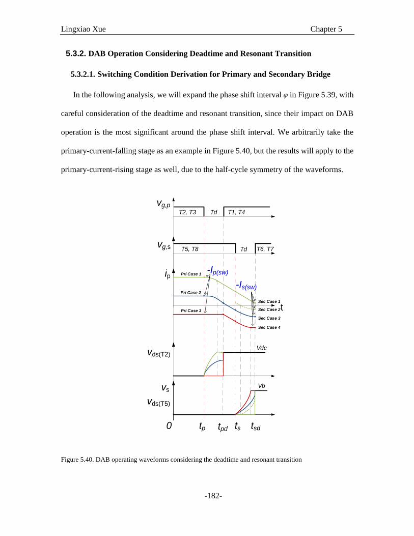
Lingxiao Xue Chapter 5
-182-
5.3.2. DAB Operation Considering Deadtime and Resonant Transition
5.3.2.1. Switching Condition Derivation for Primary and Secondary Bridge
In the following analysis, we will expand the phase shift interval φ in Figure 5.39, with
careful consideration of the deadtime and resonant transition, since their impact on DAB
operation is the most significant around the phase shift interval. We arbitrarily take the
primary-current-falling stage as an example in Figure 5.40, but the results will apply to the
primary-current-rising stage as well, due to the half-cycle symmetry of the waveforms.
ip
t
vg,p
vg,s
tp
-Ip(sw)
T2, T3
vds(T2)
T1, T4
Vdc
vsVb
T5, T8 T6, T7
vds(T5)
ts
Td
Td
Pri Case 1
Pri Case 2
Pri Case 3
Sec Case 1
Sec Case 2
Sec Case 3
Sec Case 4
-Is(sw)
0 tpd tsd
Figure 5.40. DAB operating waveforms considering the deadtime and resonant transition

Lingxiao Xue Chapter 5
-183-
The analysis is based on positive power flow where the secondary bridge lags the
primary bridge, but this idea can be easily extended to the reversed power flow. In the
figure, the gate signals Vg,p and Vg,s and the drain-to-source voltages of the representing
switches Vds(T2) and Vds(T5) are shown. Inductor current ip is also plotted to better explain
the operation. The switches are numbered according to Figure 5.37. The waveforms in this
figure are associated with the second phase shift interval φ in Figure 5.39.
The analysis starts with the state where T2 and T3 are on at the primary bridge, and T5
and T8 are on at the secondary side. The initial inductor current equals to -Ip(sw) in Figure
5.39 before T2 and T3 are turned off at tp. The captured interval between 0 and tp is merely
for demonstration purposes and its duration is extremely short, so the current level is
depicted as constant. From the instant that the primary conducting switches T2 and T3 are
turned off at tp, to the instant that the secondary conducting switches T5 and T8 are turned
off, there are three operational cases, depending on the initial current level and the circuit
component parameters at the primary side. During this interval, no switching action
happens at the secondary side, so the secondary side only exhibits as a constant voltage
source to the primary side.
Primary-Side Case 1: Primary Side Zero-Voltage-Switching (ZVS).
In this case, the initial inductor current is positive, so when T2 and T3 are turned off,
the inductor will resonate with the output capacitances of all four switches at the primary
side. The equivalent circuit is shown in Figure 5.41.

Lingxiao Xue Chapter 5
-184-
Cdc
+
-
Vdc NpsVb
Llk
T1
T2
T3
T4
+- vp
From
AC/DC
stage
ip
C2C4
C3
C1
Figure 5.41. Equivalent circuit of the resonant transition for the primary side
It is assumed that all the switches are the same, so the output capacitances are also the
same. To deal with the nonlinearity of the output capacitance, the equivalent capacitance
obtained from the output charge characterization in (2.10) is used. The differential
equations to describe this transition are obtained by KCL and KVL laws as
2 2( )C dc Coss oss p
dv d V vC C i
dt dt
(5.20)
2 2
p
lk ps b C dc C
diL N V v V v
dt (5.21)
The initial condition of the inductor current and the capacitor voltage are -Ip(sw) and 0,
respectively. Then the solutions are
2,pri_ ( )
1 cos[ ( )] sin[ ( )]( ) ( ) ( )
2 2
pri p pri p
C res dc ps b pri p sw
t t t tv t V N V Z I
(5.22)
,pri_ ( )
0
( ) sin[ ( )] ( ) cos[ ( )]dc ps b
p res pri p p sw pri p
V N Vi t t t I t t
Z
(5.23)
where
1
, lkpri pri
osslk oss
LZ
CL C (5.24)

Lingxiao Xue Chapter 5
-185-
The subscripts “pri_res” designate that the quantities are correspondent to the resonant
transition at the primary side. Also, note that both ωpri and Zpri are the functions of the Vdc
voltage, due to the nonlinearity of the output capacitance of Coss. In case 1, the capacitor
voltage vc2 can resonate from 0 volts to the DC bus voltage Vdc by the end of the dead time
Td, and then the switches T1 and T4 will conduct current in the reverse direction with a low
voltage drop. Therefore, zero-voltage-switching can be achieved when T1 and T4 are
turned on later. The condition for Case 1 is
( ) 2, _0, ( )p sw C pri res p d dcI v t T V (5.25)
The time required for the resonance process to reach the bus voltage can be obtained by
equating (5.22) to Vdc, and its solution is
1 1
_ 12 2
0 ( ) 0( ) 0
1[sin ( ) tan ( )]
( ) ( )
dc ps b dc ps b
pri res
p swdc ps b p sw
V N V V N Vt
I ZV N V I Z
(5.26)
At the rest of the deadtime, T1 and T4 will conduct in the reverse direction and generate
conduction loss. Until ts, when the secondary switches T5 and T8 are turned off, the
inductor current will decrease linearly by the excitation of Vdc+NpsVdc, which yields
, _ 1 , _ _ 1 _ 1( ) ( ) ( )dc ps b
p pri lin p pri res pri res pri res
lk
V N Vi t i t t t
L
(5.27)
Primary-Side Case 2: Primary Side Partial Zero-Voltage Switching
In this case, similar resonance happens between the DAB inductor and the output
capacitances of the switches. The governing equations will still be (5.22) to (5.24).
However, the inductor energy is not enough to bring the capacitor voltage of T2 and T3 to
the DC bus voltage. The condition for Case 2 is

Lingxiao Xue Chapter 5
-186-
( ) 2, _0, ( )p sw C pri res p d dcI v t T V (5.28)
Accordingly, the residual charge of T1 and T4 will be dissipated during the turn-on at
tpd, and partial-ZVS happens as a result. At the end of the deadtime (or the instant of tpd),
the voltage across the switch T2, and the inductor current can be easily obtained as
vc2,pri_res(tpd) and ip,pri_res(tpd) by (5.22) to (5.24). Between tpd and ts, the inductor current
changes linearly by following
, _ 2 , _( ) ( ) ( )dc ps b
p pri lin p pri res pd pd
lk
V N Vi t i t t t
L
(5.29).
Note that we have ignored the case in which the inductor current has resonated below
zero before the deadtime ends. The deadtime is selected to be slightly lower than one-
quarter of the resonant period
2
4
lk oss
d
L CT
(5.30)
so that the voltage in (5.22) will always be at the rising edge and no voltage bumping as
described in [28] occurs to cause higher loss.
Primary-Side Case 3: Primary Side Hard-Switching
In this case, the initial inductor current at tp is negative. This means at turn-off of the
switches T2 and T3, the current is flowing from to source to drain in synchronous rectifier
mode. Therefore, the turn-off of the gate will not directly cause the drain-to-source voltage
swing, and thus the inductor will be excited by the same voltage. The current change during
the deadtime is negligible due to low voltage slew rate (Vdc - NpsVb) / Llk. so it is assumed
to be constant. At tpd, when T1 and T4 will be turned on in hard-switching conditions, the
Vds(T2) rises with a much higher slew rate than that of the turn-off transition. As a result,

Lingxiao Xue Chapter 5
-187-
the inductor current remains almost unchanged until the end of the deadtime tpd. After tpd,
the inductor current will decrease in the form of
, _ 3 ( )( ) ( )dc ps b
p pri lin p sw pd
lk
V N Vi t I t t
L
(5.31)
Moreover, the condition for Case 3 is
( ) 0p swI (5.32)
Summarizing the three cases, at ts when the secondary switches T5 and T8 are turned
off, the inductor current ip should be
, _ 1 ( ) 2, _
, _ 2 ( ) 2, _
, _ 3 ( )
( ) 0, ( ) ( 1)
( ) ( ) 0, ( ) ( 2)
( ) 0 ( 3)
p pri lin s p sw C pri res pd dc
p s p pri lin s p sw C pri res pd dc
p pri lin s p sw
i t if I v t V Case
i t i t if I v t V Case
i t if I Case
(5.33).
This current will be used to determine the operational cases of the secondary side.
Meanwhile, the capacitor voltage vc2 can also be summarized as
( ) 2, _
2 2, _ ( ) 2, _
( )
0, ( ) ( 1)
( ) ( ) 0, ( ) ( 2)
0 0 ( 3)
dc p sw C pri res pd dc
C pd C pri res pd p sw C pri res pd dc
p sw
V if I v t V Case
v t v t if I v t V Case
if I Case
(5.34)
This voltage will be used to estimate the switching loss of primary-side switches.
At ts, the switches T6 and T7 from the secondary full-bridge are turned on. There are
four operational cases, depending on the initial value of the inductor current at ts and the
circuit parameters. It is worth mentioning that the primary-side cases do not directly
correspond to the secondary-side cases, but their effects on the inductor current at ts do
determine which secondary-side case the converter will be operated in. For example, a
DAB converter whose primary switches operate in primary-side case 1 can either have its

Lingxiao Xue Chapter 5
-188-
secondary switches fall into the secondary-side case 3 or secondary-side case 4, depending
on the inductor current at ts.
Secondary-Side Case 1: Secondary Switches Hard-Switching
In this case, the initial inductor at the turn-off of T5 and T8 will remain positive even
by the end of the deadtime of the secondary side switches (instant tsd). The inductor current
will decrease following
,sec_lin1( ) ( ) ( )dc ps b
p p s s
lk
V N Vi t i t t t
L
(5.35)
The subscript “sec” designates that the quantities are related to secondary side transition.
So the condition of case 1 is
,sec_lin1( ) 0, ( ) 0p s p sdi t i t (5.36)
The switch voltage change is negligible because the current will continue flowing through
T5 and T8 in the reverse direction with a slight increase in the voltage drop.
Secondary-Side Case 2: Secondary Switches Partial Zero-Voltage-Switching with
Positive Initial Current
In this case, the initial current at the turn-off of T5 and T8 is positive, but the current is
reduced to negative thanks to the high voltage excitation that equals to (Vdc + NpsVb) / Llk.
This is different from the Primary-side case 3 where the voltage excitation is much lower,
and the current change is negligible. The time required for the inductor current to fall to
zero is calculated as
sec_ 2 ( ) lklin p s
dc ps b
Lt i t
V N V
(5.37)

Lingxiao Xue Chapter 5
-189-
When the current falls to zero, the resonance process starts. The equivalent circuit for the
secondary side resonance is shown in Figure 5.42. Note that the primary quantities have
been referred to the secondary side.
+
Vdc/Nps
+
-Vb
T5
T6
T7
T8
-+ -vs
IbipNps
2/lk psL N
Figure 5.42. Equivalent circuit of the resonant transition for the secondary side
Similar equations to the primary-side resonant transition can be obtained, they are
5 5( )b C Coss oss p ps
d V v dvC C i N
dt dt
(5.38)
5 52
( )0
p pslk dcb C C
ps ps
d i NL VV v v
N dt N (5.39)
The initial capacitor voltage is zero, and if assuming the initial inductor current is ip,sec_ini,
the solution of the above differential equations is
sec sec5,sec_ p,sec_ini sec ,sec_
1 cos[ ( )] sin[ ( )]( , , ) ( ) ( )
2 2
dc start startC res start b p ini
ps
V t t t tv t t i V Z i
N
(5.40)
,sec_ p,sec_ini sec ,sec_ sec
sec
1( , , ) ( ) sin[ ( )] ( ) cos[ ( )]dc
p res start b start p ini start
ps
Vi t t i V t t i t t
Z N
(5.41)
where

Lingxiao Xue Chapter 5
-190-
sec sec
1,
ps lk
ps osslk oss
N LZ
N CL C (5.42)
and tstart is the start time of the resonant process. For secondary side case 2, we know tstart
= ts + tsec_lin2, and the initial inductor current Ip,sec_ini = 0. Therefore, at the end of the
deadtime or the instant of tsd, the inductor current will be ip,sec_res(tsd, ts + tsec_lin2, 0), and the
capacitor voltage will be vc5,sec_res(tsd, ts + tsec_lin2, 0). The condition for this secondary side
case 2 is given by
,sec_lin1( ) 0, ( ) 0p s p sdi t i t (5.43)
In this case 2, if the deadtime is long enough, the capacitor voltage should finally reach
the battery voltage, even if the initial inductor energy is zero. However, this fixed deadtime
will be too long for other conditions where the inductor does have enough energy. This
will lead to high reverse conduction losses. Adaptive deadtime could be implemented, but
will not be used in this work due to increased complexity. Instead, we selected the deadtime
whose value equals to the primary side switches. The length of the deadtime is not enough
to swing the switch capacitance voltage up to the full battery voltage given zero initial
current of the inductor. What is more, even when the inductor has some low initial energy
at the beginning of the resonant transition, it might not be sufficient to fully charge and
discharge the switch capacitances, as will be quantified in the following section: Secondary
Side Case 3.
Secondary-Side Case 3: Secondary Switches Partial Zero-Voltage-Switching with
Negative Initial Current
In this case, the initial current at ts is negative. This will directly initiate the resonant
transition governed by the same equations of (5.40) to (5.42) only with the initial current

Lingxiao Xue Chapter 5
-191-
ip,sec_ini = ip(ts). Within the deadtime, the initial inductor energy is not enough to fully charge
the capacitor so that the final capacitor voltage will be vc5,sec_res(tsd, ts , ip(ts)). Accordingly,
the inductor current at the end of the deadtime will be ip,sec_res(tsd, ts , ip(ts)). The condition
to make this case happen is
5,sec_res( ) 0, ( )p s C sd bi t v t V (5.44)
Secondary-Side Case 4: Secondary Switches Zero-Voltage-Switching
The last case happens when the inductor has enough initial energy at ts, which can bring
the capacitor voltage to the battery voltage Vb by the end of the deadtime. The key equations
are still (5.40) to (5.42). The time required to fully charge the capacitor can be obtained by
equating (5.40) to Vb, and the solution is
1 1
sec_ 42 2
sec secsec
/ /1[sin ( ) tan ( )]
( )( / ) ( ( ) )
b dc ps dc ps b
res
p sdc ps b p s
V V N V N Vt
i t ZV N V i t Z
(5.45)
At the rest of the deadtime, T6 and T7 will conduct in the reverse direction and generate
conduction loss. The inductor current will change linearly as a result of the excitation of
Vdc-NpsVdc, but this change is very small, and so it is neglected. The condition of this case
is summarized as
5,sec_res( ) 0, ( )p s C sd bi t v t V (5.46)
Summarizing the four cases of the secondary side, at tsd when the secondary switches
T6 and T7 are turned on, the inductor current ip should be

Lingxiao Xue Chapter 5
-192-
,sec_lin1 ,sec_lin1
,sec_lin1
5,sec_re
,
s
_ _ 2
, _
, e_ s
( ) ( ) 0, ( ) 0 ( 1)
( ) 0, ( ) 0 ( 2)( )
( ) 0, ( ) ( 3
, , 0
, , )
p sec res sd s sec lin
p sec re
p sd p s p sd
p s
s sd s p s
p sec res sd
p sd
p sd
p s C sd b
i t if i t i t Case
if i t i t Casei t
if i t v t V Case
i t t t
i t t i t
t ti
c_ 4 5,sec_res( ) 0, ( ) ( 4, , )res p s C ss p s d bif i t v t V Ct i t ase
(5.47)
Meanwhile, the capacitor voltage vc2 can also be summarized as
5,
,sec_lin1
_ _ 2
5, _
,sec_lin1
5
5,sec_res
5,sec_res
0 ( ) 0, ( ) 0 ( 1)
( ) 0, ( ) 0 ( 2)( )
( ) 0, ( ) ( 3)
( ) 0, ( )
, , 0
, ,
p s p sd
p s p sc sec res sd s sec lin
c sec res s
d
C sd
p s C sd b
b p s
s s
C s
d p
d
v t
if i t i t Case
if i t i t Casev t
if i t v t V Case
V if
t t
v t t i
i t v
t
t
( 4)bV Case
(5.48)
This voltage will be used to estimate the switching loss of the secondary side switches.
5.3.2.2. Switching Condition Boundaries
In a battery charger application, the DAB converter operates in the wide range of
battery voltage and charging current. This wide load range introduces the DAB converter
into different switching conditions as derived in the previous section. It will be beneficial
to show the different conditions on the load profile map of the battery current and battery
voltage, so it is clear which condition the charger is operated under. In this section, the
boundary lines between different operating conditions are plotted, and the load profile map
is divided into several regions accordingly.
For the primary side, the boundary between the hard switching and the partial ZVS is
determined by making (5.32) zero:
( ) 0p swI (5.49)

Lingxiao Xue Chapter 5
-193-
The boundary between the partial ZVS and the ZVS can be obtained by (5.25) in which
the output capacitance is just fully charged at the end of the deadtime:
2, _ ( )C pri res p d dcv t T V (5.50)
For the secondary side, the calculations are more difficult because, as will be described
in the next section, the phase shift of gate signals (or the instant ts in Figure 5.40) requires
correction to account for the switching delays. The delays will impact the derivation of the
secondary side currents. A simplification is made by ignoring the Secondary side case 2,
and directly using
s( ) 0swI (5.51)
which gives a good estimation. The boundary between partial ZVS and ZVS is obtained
by
5,sec_ ( , , ( ))C res sd s p s bv t t i t V (5.52)
At the boundary, since the output capacitance is charged to the full DC voltage using the
entire deadtime, one-half of the deadtime is assumed as the switching delay, which yields
the initial current of (5.52)
( )( ) ( )2
dc ps b dp s p sw s pd
lk
V N V Ti t I t t
L
(5.53)
Here ts is the real phase shift between the two excitation voltages Vp and Vs across the
DAB inductor, not the gate signals. The impact of the timing difference between the gate
signals and the excitation voltages due to switching delay will be detailed in the following
section. Solving the battery current ib with respect to the battery voltage Vb from the
boundary equations from (5.49) to (5.53) will lead to the boundary solutions. An example

Lingxiao Xue Chapter 5
-194-
plot of the boundary solutions is shown in Figure 5.43. The DAB parameters used in this
chart are summarized in Table 5.3. The output capacitance of the GaN switch is obtained
from the curve fitting of the characterization results from Section 2.3.3. Those parameters
are used to match with the measurement conditions in Section 5.3.3.4.
190 200 220 240 250
0
2
4
6
8
Battery Voltage Vb (V)
Bat
tery
Curr
ent
I b (
A)
P: ZVS
S: HS
P: ZVS
S: PZVS
P: ZVS
S: ZVS
P: PZVS
S: ZVS
P:HS
S:ZVS
P: HS
S: PZVS
P:PZVS
S:HS
P: PZVS
S: PZVS
Figure 5.43. DAB operation regions in term of switching conditions.
Table 5.3. DAB parameters used to plot the switching condition chart
Input voltage Vdc (V) 220
Battery voltage Vb (V) 190 - 250
DAB inductance Llk (uH) 3.25
DAB transformer turns ratio 1:1
Switching frequency (kHz) 500
The blue regions are related to the primary side, while the red regions are related to
the secondary side. We can see that the primary switches experience hard-switching (HS),
Lingxiao Xue Chapter 5
-195-
partial-zero-voltage-switching (PZVS), and finally zero-voltage-switching (ZVS) from the
left-lower corner to the right-upper corner. Similarly, the secondary switches experience
HS, PZVS and ZVS from the right-lower corner to the left-upper corner. The different
operating conditions of primary and secondary switches combine with each other and form
eight distinct regions. It is clear that at higher battery currents, it is easier to achieve soft-
switching.
The switching conditions are very important to predict the DAB losses. Furthermore,
at different switching conditions, the switching delay between the gate signals and the
excitation voltage of the inductor also changes, which is very critical for modeling the DAB
current and voltage waveforms. We will explain this in the following section.
5.3.2.3. Correction on the Gate Signals Timing
If all the derivations and assumptions in section 5.3.2.1 are valid, at tsd, the inductor
current should equal to the current value of ip(tsd) = –Is(sw) in Figure 5.40. The results of
Is(sw) in (5.19) and ip(tsd) in (5.47) are compared in Figure 5.44. The DAB parameters are
the same as those listed in Table 5.3. The -Is(sw) value is not impacted by the deadtime and
only weakly impacted by the resonant transition, so it can be treated as the “real” current
and is plotted as the solid line. The modeled ip(tsd) from the previous section is shown as
the dashed line. We can see high discrepancy at low battery current, especially when the
battery VbNps/Vdc value is not around 1. As the battery current gets high, the two curves
finally merge with each other, so that the model is correct at high current. However, an
accurate model at low current for a DAB with sinusoidal charging is very important for
predicting DAB loss, so the model needs to be improved.
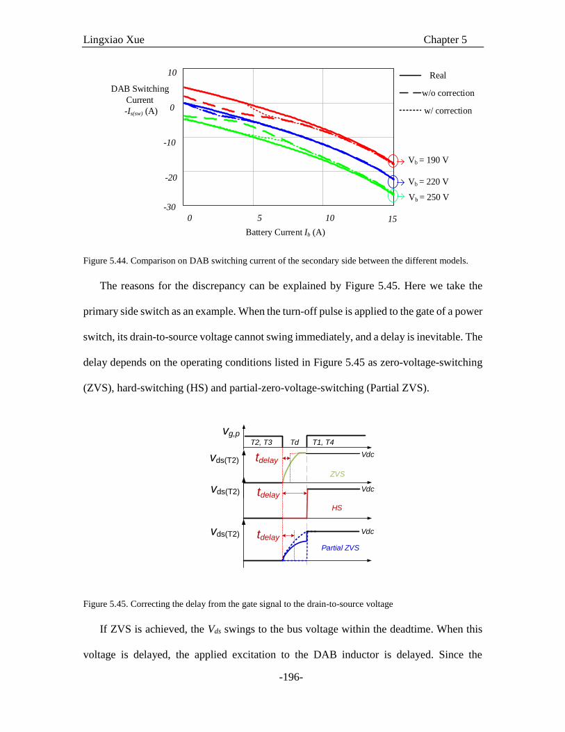
Lingxiao Xue Chapter 5
-196-
Real
w/o correction
0 5 10 15
Battery Current Ib (A)
Vb = 190 V
Vb = 220 V
Vb = 250 V-30
-20
-10
0
10
DAB Switching
Current
-Is(sw) (A) w/ correction
Figure 5.44. Comparison on DAB switching current of the secondary side between the different models.
The reasons for the discrepancy can be explained by Figure 5.45. Here we take the
primary side switch as an example. When the turn-off pulse is applied to the gate of a power
switch, its drain-to-source voltage cannot swing immediately, and a delay is inevitable. The
delay depends on the operating conditions listed in Figure 5.45 as zero-voltage-switching
(ZVS), hard-switching (HS) and partial-zero-voltage-switching (Partial ZVS).
vg,pT2, T3
vds(T2)
T1, T4
Vdc
Td
Vdc
vds(T2)
HS
ZVS
tdelay
tdelay
vds(T2) Vdc
Partial ZVS
tdelay
Figure 5.45. Correcting the delay from the gate signal to the drain-to-source voltage
If ZVS is achieved, the Vds swings to the bus voltage within the deadtime. When this
voltage is delayed, the applied excitation to the DAB inductor is delayed. Since the

Lingxiao Xue Chapter 5
-197-
excitation voltage changes within the ZVS transition, we use half of the resonant transition
time in (5.26) as the delay time. In this way, equivalently a step voltage is used to represent
the original resonant waveform by providing a similar amount of charge. In the case of HS,
the full deadtime is accounted as the delay.
Special attention is paid to the partial ZVS case, where two extreme points are
identified: the capacitor fully charged or not charged at all within the deadtime. For the
first point where the capacitor is fully charged within the deadtime, the delay is
approximated by half of the deadtime. For the second point where the capacitor is not
charged, the delay time equals to the entire deadtime, the same as that of the hard-switching
case. The battery current of the two points can be solved by the equations of (5.50) and
(5.49), respectively. A linear extrapolation anchored by the two extreme points is used to
fit the partial ZVS cases in between. In all, the delay for those three cases is summarized
as
_ 1
,
, _ _
, _ _ , _ _
/ 2
/ 2( ( ))
( ) ( ) 2
pri res
delay p d
d d d
b b pri bdr PZVS b
b pri bdr HS b b pri bdr PZVS b
t if ZVS
t T if HS
T T Ti I V if Partial ZVS
I V I V
(5.54)
in which Ib,pri_bdr_HS(Vb) is the battery current at the boundary of HS and partial-ZVS regions,
and Ib,pri_bdr_PZVS(Vb) is the battery current at the boundary of partial-ZVS and ZVS regions.
This mechanism of time delay also applies to the secondary side, because the existence
of the two boundary lines between HS and partial-ZVS, and between partial-ZVS and ZVS.
For the ZVS case, we cannot directly use half the resonant transition time in (5.45) as the

Lingxiao Xue Chapter 5
-198-
delay time, because ip(ts) in the equation is no longer accurate if the switching transition
delay is considered. The instant ts reflects the phase shift between the gate signals of two
sides of DAB, but not the excitation voltages due to delays. In order to solve the correct
transition time, the following two equations are used:
5,sec_ ( , , ( ))C res x s p s bv t t i t V (5.55)
( )( ) ( )2
dc ps b xp s p sw pd
lk
V N V ti t I t t
L
(5.56)
where tx is the transition time of the secondary side. Note that here we assumed the primary
side is doing hard switching. This assumption can simplify the equation solving process by
avoiding the conditional decision. Similarly to that of the primary side, the HS case has a
delay time of one deadtime Td. For the partial ZVS case, two extreme points are identified
from the two boundary lines among HS, partial-ZVS and ZVS cases. The equations used
are from (5.49) to (5.53). The resultant delay time is summarized in the following for
different cases
sec_ 4
,
,sec_ _
,sec_ _ ,sec_ _
/ 2
/ 2( ( ))
( ) ( ) 2
res
delay p d
d d d
b b bdr PZVS b
b bdr HS b b bdr PZVS b
t if ZVS
t T if HS
T T Ti I V if Partial ZVS
I V I V
(5.57)
With this delay time considered, the current at the turn-on instant of the secondary
switch at ts in (5.33) is updated. Accordingly, the switching current of the secondary side
in (5.47) is also changed. The results with the gate signal correction are shown as the dotted
line in Figure 5.44. It can be seen that the discrepancy with the correction is significantly

Lingxiao Xue Chapter 5
-199-
reduced compared to the dashed line without correction, especially at low battery current.
Certain error still exists at the mid-current range due to the assumption of (5.56). However,
the accuracy is enough for loss estimation purposes, as we can see in the next section.
5.3.3. GaN DAB Converter Loss Modeling
5.3.3.1. Conduction Loss of the GaN Module
The switching conditions derived in the previous section are very important to model
DAB losses. The RMS value of the DAB inductor current has been shown as (4.15) in
section 4.2.2.3. The conduction loss is therefore re-written as
2 2
( )_ ( )(1 )2 pcon DAB slk rms ds on
p i R N (5.58)
But with
( ),ZVS
( ),( )
( )
( )
ds on sw
ds on HS swds on
R V if ZVS
R V if HS and PZVSR
(5.59)
This means that the dynamic on-resistance of the GaN module changes needs to be
considered according to different switching conditions, as has been characterized in section
2.3.2 of chapter 2. Vsw is the switching voltage applied across the device before it is turned
on. For partial ZVS (PZVS) cases, the switching voltage is not the full DC bus voltage but
the remaining voltage after the discharging process.
5.3.3.2. Switching Loss of the GaN Module
The switching loss can be determined by switching current, switching voltage and the
output charge of the GaN module. For the GEN 4 GaN module, the turn-off loss is
negligible due to the very short overlap between channel current and drain-source voltage,
so only turn-on energy is taken into account. The energy loss models for HS, ZVS, and

Lingxiao Xue Chapter 5
-200-
partial-ZVS cases are different. The turn-on energy is summarized as the following
equation.
,eq
,eq
( ) 0.5
( , ) ( ) 0.5
( ) ( )
oss sw sw sw sw sw sw
sw sw sw oss sw sw sw sw sw sw
f sw sw d res
C V V V t V I if HS
E V I C V V V t V I if PZVS
V I I T t if ZVS
(5.60)
in which Vsw and Isw are the switching voltage and current; tsw is the switching time; and
Coss,eq(Vsw) is the equivalent output capacitance at Vsw of either the top or the bottom
switches array in the GaN module as characterized and defined in (2.10) of section 2.3.3.
In the case of ZVS, there is no turn-on loss. However, as the output capacitance is fully
discharged before the deadtime ends, this switch will conduct in “diode” mode with a high
voltage drop. We put this deadtime-conduction loss in the switching energy equation for
more concise and clear formulation.
In the case of HS, the consumed energy consists of two parts, the capacitance-related
energy loss and the voltage-current overlapping loss. From off state to on state, the turn-on
switch will dissipate the energy of its output capacitance. Also, the output capacitance of
the complementary switch will be charged to the full voltage by the DC source through the
channel of the turn-on switch, generating energy loss. Considering a two phase leg with
two identical (top and bottom) switches, those two parts of energy loss will add up to
Qoss,eq(Vsw)·Vsw = Coss,eq(Vsw) ·Vsw. Note that this energy is also valid even if the capacitance
nonlinearity is considered [29]. The second part of the energy loss is associated with the
overlapping between the switching voltage and current. The switching time can be obtained
by measurements.
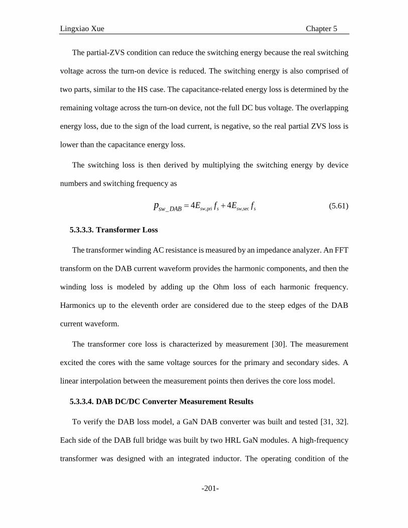
Lingxiao Xue Chapter 5
-201-
The partial-ZVS condition can reduce the switching energy because the real switching
voltage across the turn-on device is reduced. The switching energy is also comprised of
two parts, similar to the HS case. The capacitance-related energy loss is determined by the
remaining voltage across the turn-on device, not the full DC bus voltage. The overlapping
energy loss, due to the sign of the load current, is negative, so the real partial ZVS loss is
lower than the capacitance energy loss.
The switching loss is then derived by multiplying the switching energy by device
numbers and switching frequency as
,pri ,sec_ 4 4sw s sw ssw DAB E f E fp (5.61)
5.3.3.3. Transformer Loss
The transformer winding AC resistance is measured by an impedance analyzer. An FFT
transform on the DAB current waveform provides the harmonic components, and then the
winding loss is modeled by adding up the Ohm loss of each harmonic frequency.
Harmonics up to the eleventh order are considered due to the steep edges of the DAB
current waveform.
The transformer core loss is characterized by measurement [30]. The measurement
excited the cores with the same voltage sources for the primary and secondary sides. A
linear interpolation between the measurement points then derives the core loss model.
5.3.3.4. DAB DC/DC Converter Measurement Results
To verify the DAB loss model, a GaN DAB converter was built and tested [31, 32].
Each side of the DAB full bridge was built by two HRL GaN modules. A high-frequency
transformer was designed with an integrated inductor. The operating condition of the

Lingxiao Xue Chapter 5
-202-
converter is the same as those summarized in Table 5.3.. The DAB converter was not tested
to the full voltage and full power of 3.3 kW because of the GaN device limitations.
The modeled conduction loss of the GaN switches is shown in Figure 5.46. We can see
that at low current, Vb = 220V provides the lowest conduction loss. This is because the
current waveform under this condition is the closest to a square wave. At the high current
side, the conduction loss of the high battery voltage case becomes higher, due to increased
output power.
Vb = 190 V
Vb = 220 V
Vb = 250 V
GaN
Co
nd
uct
ion
Lo
ss
(W)
0 2 4 6 8
0
20
40
60
80
10
Battery Current Ib (A)
Figure 5.46. Modeled GaN device conduction loss of the DAB converter
The modeled DAB switching loss of the GaN switches is shown in Figure 5.47. All
three curves show turning points at certain current levels due to the boundaries of HS/PZVS
and PZVS/ZVS. At very low current, Vb=220V shows the highest loss because both sides
of the DAB are PZVS switching, while for Vb=250V and Vb=190V, one side of the DAB
can achieve ZVS. At very high current, all three cases can achieve ZVS. Therefore, the
switching loss becomes low and only depends on the conduction loss during the deadtime.
In the medium current levels, the loss curves transit from the high level to the low level
gradually with the increase of battery current, reflecting the effect of partial ZVS.
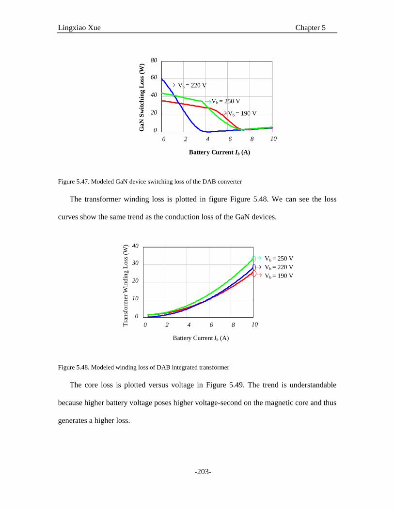
Lingxiao Xue Chapter 5
-203-
Vb = 190 V
Vb = 220 V
Vb = 250 V
Ga
N S
wit
chin
g L
oss
(W
)0 2 4 6 8
0
20
40
60
80
10
Battery Current Ib (A)
Figure 5.47. Modeled GaN device switching loss of the DAB converter
The transformer winding loss is plotted in figure Figure 5.48. We can see the loss
curves show the same trend as the conduction loss of the GaN devices.
Vb = 190 V
Vb = 220 V
Vb = 250 V
Tra
nsf
orm
er W
indin
g L
oss
(W
)
0 2 4 6 8
0
10
20
30
40
10
Battery Current Ib (A)
Figure 5.48. Modeled winding loss of DAB integrated transformer
The core loss is plotted versus voltage in Figure 5.49. The trend is understandable
because higher battery voltage poses higher voltage-second on the magnetic core and thus
generates a higher loss.
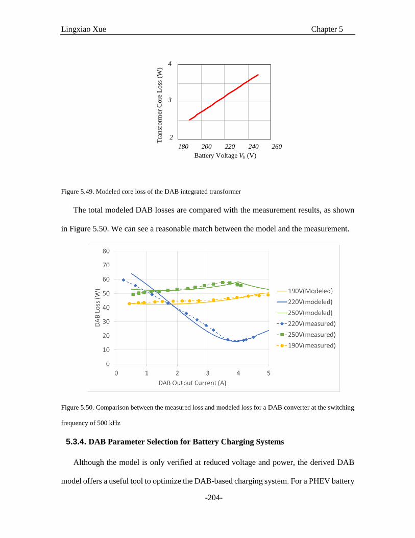
Lingxiao Xue Chapter 5
-204-
Tra
nsf
orm
er C
ore
Loss
(W
)
180 200 220 240 260
2
3
4
Battery Voltage Vb (V)
Figure 5.49. Modeled core loss of the DAB integrated transformer
The total modeled DAB losses are compared with the measurement results, as shown
in Figure 5.50. We can see a reasonable match between the model and the measurement.
Figure 5.50. Comparison between the measured loss and modeled loss for a DAB converter at the switching
frequency of 500 kHz
5.3.4. DAB Parameter Selection for Battery Charging Systems
Although the model is only verified at reduced voltage and power, the derived DAB
model offers a useful tool to optimize the DAB-based charging system. For a PHEV battery
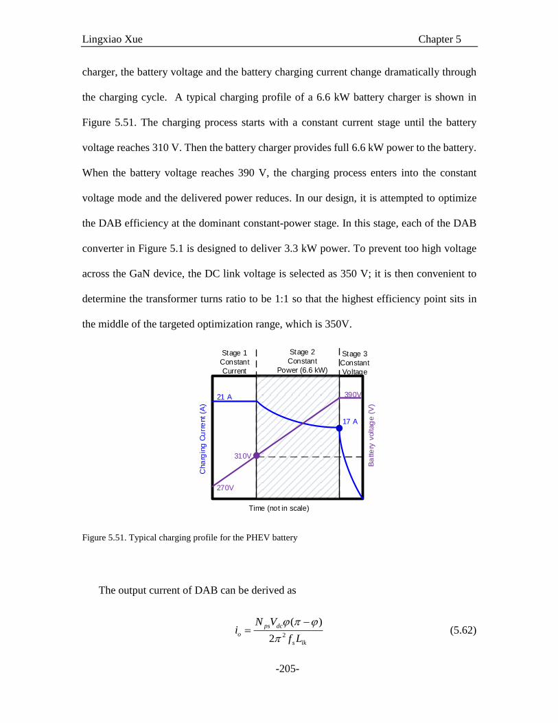
Lingxiao Xue Chapter 5
-205-
charger, the battery voltage and the battery charging current change dramatically through
the charging cycle. A typical charging profile of a 6.6 kW battery charger is shown in
Figure 5.51. The charging process starts with a constant current stage until the battery
voltage reaches 310 V. Then the battery charger provides full 6.6 kW power to the battery.
When the battery voltage reaches 390 V, the charging process enters into the constant
voltage mode and the delivered power reduces. In our design, it is attempted to optimize
the DAB efficiency at the dominant constant-power stage. In this stage, each of the DAB
converter in Figure 5.1 is designed to deliver 3.3 kW power. To prevent too high voltage
across the GaN device, the DC link voltage is selected as 350 V; it is then convenient to
determine the transformer turns ratio to be 1:1 so that the highest efficiency point sits in
the middle of the targeted optimization range, which is 350V.
Cha
rgin
g C
urr
ent
(A)
Ba
tte
ry v
oltag
e (
V)
Stage 1
Constant
Current
Stage 2
Constant
Power (6.6 kW)
Stage 3
Constant
Voltage
21 A
310V
390V
270V
Time (not in scale)
17 A
Figure 5.51. Typical charging profile for the PHEV battery
The output current of DAB can be derived as
2
( )
2
ps dc
o
s lk
N Vi
f L
(5.62)

Lingxiao Xue Chapter 5
-206-
in which Nps is transformer turns ratio from primary to secondary sides, Vdc is the DC link
voltage, φ is the phase shift angle, fs is the switching frequency, Vb is the battery voltage,
and Llk is the commutation inductance. Meanwhile, the battery charger output current can
be in the form of
( ) (1 cos 2 )o oi t I t (5.63)
which is designated as sinusoidal charging in [33, 34] with the intent to reduce the DC link
capacitance. In this case, the output current will be regulated by controlling the phase shift
φ through the line cycle. The peak value of (5.62) occurs when the phase angle equals to
π/2. Then the peak current the DAB can deliver is plotted as the solid line in Figure 5.52
with different commutation inductance value. By doing sinusoidal charging in (5.63), the
peak output current will be twice the average value. Therefore to deliver full 3.3 kW power
at 310 V, the DAB commutation inductance should be lower than 4 µH, as shown in Figure
5.52. In practice, the current gain of DAB becomes too low when phase shift gets close to
π/2, which will make sinusoidal charging control difficult. Therefore, the inductance
should be much lower than 4 µH.
One of the main benefits of the DAB converter is the capability of soft-switching turn-
on for all eight switches. With the phase shift modulation, the DAB switching condition
boundaries at the map of battery voltage and charging current are shown in Figure 5.53
with two commutation inductance values (2 µH and 4 µH). For each inductance value, four
boundary lines can be identified to divide the map into eight regions, as has been illustrated
in Figure 5.43. We can also clearly see that the boundaries lines with a high inductance (4
µH) are lower than those with low inductance, which means less load current requirement
and a wider soft-switching range.
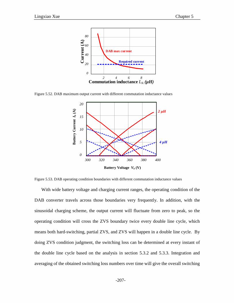
Lingxiao Xue Chapter 5
-207-
0
20
40
60
80
2 4 6 8
Commutation inductance Llk (µH)C
urren
t (A
)
DAB max current
Required current
Figure 5.52. DAB maximum output current with different commutation inductance values
300 320 340 360 380 400
0
5
10
15
20
2 µH
4 µH
Battery Voltage Vb (V)
Ba
tter
y C
urr
ent
Ib (
A)
Figure 5.53. DAB operating condition boundaries with different commutation inductance values
With wide battery voltage and charging current ranges, the operating condition of the
DAB converter travels across those boundaries very frequently. In addition, with the
sinusoidal charging scheme, the output current will fluctuate from zero to peak, so the
operating condition will cross the ZVS boundary twice every double line cycle, which
means both hard-switching, partial ZVS, and ZVS will happen in a double line cycle. By
doing ZVS condition judgment, the switching loss can be determined at every instant of
the double line cycle based on the analysis in section 5.3.2 and 5.3.3. Integration and
averaging of the obtained switching loss numbers over time will give the overall switching

Lingxiao Xue Chapter 5
-208-
loss. Figure 5.54 plots the switching loss at three different battery voltage by sweeping the
commutation inductance value up to 4 µH. We can see that the switching loss decreases
with higher commutation inductance, thanks to extended ZVS range. Inductance has little
influence on the switching loss in the case of Vb = 350 V because the ZVS range extension
at this point is very limited, which can be seen in Figure 5.53.
Vb = 310 V
Vb = 350 V
Vb = 390 V
GaN
Sw
itch
ing
Lo
ss (
W)
2 2.5 3 3.5
60
80
100
120
140
4
DAB Commutation Inductance Llk (µH)
Figure 5.54. Calculated switching loss at three different battery voltages by sweeping the commutation
inductance value up to 4 µH.
Similarly, we can plot the conduction loss curve with different commutation
inductances, as shown in Figure 5.55. Again, commutation inductance has more significant
impact on the conduction loss of the case of Vb = 310 V and 390 V than that of Vb = 350
V. With higher inductance, the RMS value of the inductor current increases, causing higher
condition losses. It is understandable that the lower battery voltage shows higher
conduction loss because the average output current is higher in a constant power charging
mode.

Lingxiao Xue Chapter 5
-209-
Vb = 310 V
Vb = 350 V
Vb = 390 V
GaN
Co
nd
uct
ion
Lo
ss (
W)
2 2.5 3 3.5
60
80
100
120
140
4
DAB Commutation Inductance Llk (µH)
Figure 5.55. Calculated conduction loss at three different battery voltages by sweeping the commutation
inductance value up to 4 µH.
By adding up the results in Figure 5.54 and Figure 5.55, the total GaN loss can be
obtained in Figure 5.56. However, the total loss curves show different (even opposite)
trends at different battery voltages, so it is not clear how to select the commutation
inductance value.
Vb = 310 V
Vb = 350 V
Vb = 390 V
GaN
Tota
l L
oss
(W
)
2 2.5 3 3.5
60
80
100
120
140
4
DAB Commutation Inductance Llk (µH)
Figure 5.56. Calculated GaN total loss at three different battery voltages by sweeping the commutation
inductance value up to 4 µH.
To address the issue, the total energy loss, defined as the integration of loss over the
charging time, is calculated according to the charging profile. At different charging instants,
the battery voltages and charging currents are different, so the battery charger loss will also
be different. The total energy loss during the charging cycle from 310 V to 390 V with

Lingxiao Xue Chapter 5
-210-
different commutation inductance is plotted in Figure 5.57. This result slightly differs from
the results in [31] due to improved GaN device characterization and loss modeling. We can
see the minimum loss is at Llk = 2.5 µH. A transformer with three µH integrated inductance
is finally built for the DAB stage [31].
_0
( )T
loss cyc lossE p t dt (5.64)
Figure 5.57. Total energy loss through the charging cycle with different commutation inductance
5.3.5. Summary and Conclusion
The dual active bridge converter is examined as the DC/DC stage of a battery charger
for the plug-in hybrid electric vehicle. The DAB design is challenging considering the wide
battery voltage range. If sinusoidal charging is implemented, the output current will
fluctuate at double line frequency, which further makes the parameter selection difficult.
This section investigates the DAB operating and switching conditions with great detail to
account for the cases of hard-switching, partial zero-voltage-switching, and zero-voltage-
switching, based on which the DAB loss model is derived. The loss model was verified by
experimental measurement of a 500 kHz GaN DAB converter at reduced voltage and power.
With this DAB operating and loss model, the DAB commutation inductance value is

Lingxiao Xue Chapter 5
-211-
determined to achieve minimum energy loss through the entire charging cycle. The decided
inductance value is finally integrated to a high frequency transformer.
5.4. CONSTRUCTED GAN BATTERY CHARGER PROTOTYPES
5.4.1. 1 kW GaN Battery Charger
The 1 kW breadboard charger is shown in Figure 5.58. This prototype only contains
one channel of a PFC plus DAB. Switching at 500 kHz, this charger was able to achieve
all the functions of battery charging with the bi-directional power flow. However, with
early HRL modules, low rating magnetics, and immature noise containment designs, this
charger only achieves 1 kW power as a full charging system. The measured waveforms at
1 kW output power are shown in Figure 5.59. With sinusoidal charging, the charging
system achieves 92% efficiency. With DC charging, the overall efficiency increases to 94%.
The test conditions are 165 V AC voltage, 250 V DC link voltage, 250 V battery voltage,
and 500 kHz switching frequency. Some of the old generation GaN modules suffered from
false turn-on after turn-off transition due to gate ringing, causing higher switching losses.
The discrete magnetic design was also not optimized.
Figure 5.58. Photograph of the 1 kW GaN charger
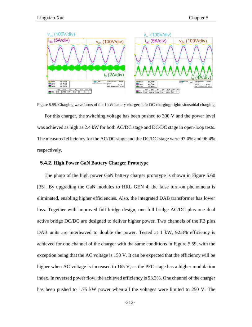
Lingxiao Xue Chapter 5
-212-
Figure 5.59. Charging waveforms of the 1 kW battery charger; left: DC charging; right: sinusoidal charging
For this charger, the switching voltage has been pushed to 300 V and the power level
was achieved as high as 2.4 kW for both AC/DC stage and DC/DC stage in open-loop tests.
The measured efficiency for the AC/DC stage and the DC/DC stage were 97.0% and 96.4%,
respectively.
5.4.2. High Power GaN Battery Charger Prototype
The photo of the high power GaN battery charger prototype is shown in Figure 5.60
[35]. By upgrading the GaN modules to HRL GEN 4, the false turn-on phenomena is
eliminated, enabling higher efficiencies. Also, the integrated DAB transformer has lower
loss. Together with improved full bridge design, one full bridge AC/DC plus one dual
active bridge DC/DC are designed to deliver higher power. Two channels of the FB plus
DAB units are interleaved to double the power. Tested at 1 kW, 92.8% efficiency is
achieved for one channel of the charger with the same conditions in Figure 5.59, with the
exception being that the AC voltage is 150 V. It can be expected that the efficiency will be
higher when AC voltage is increased to 165 V, as the PFC stage has a higher modulation
index. In reversed power flow, the achieved efficiency is 93.3%. One channel of the charger
has been pushed to 1.75 kW power when all the voltages were limited to 250 V. The
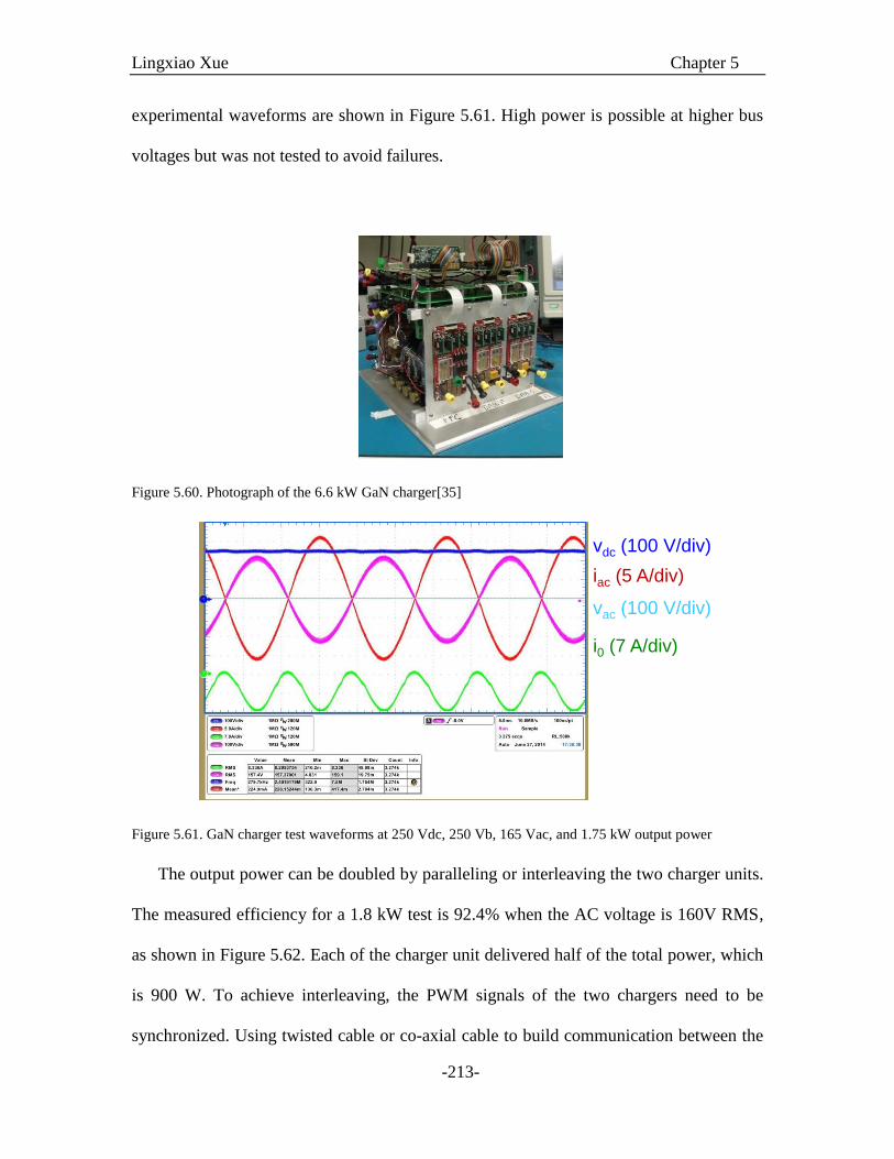
Lingxiao Xue Chapter 5
-213-
experimental waveforms are shown in Figure 5.61. High power is possible at higher bus
voltages but was not tested to avoid failures.
Figure 5.60. Photograph of the 6.6 kW GaN charger[35]
Figure 5.61. GaN charger test waveforms at 250 Vdc, 250 Vb, 165 Vac, and 1.75 kW output power
The output power can be doubled by paralleling or interleaving the two charger units.
The measured efficiency for a 1.8 kW test is 92.4% when the AC voltage is 160V RMS,
as shown in Figure 5.62. Each of the charger unit delivered half of the total power, which
is 900 W. To achieve interleaving, the PWM signals of the two chargers need to be
synchronized. Using twisted cable or co-axial cable to build communication between the
iac (5 A/div)
i0 (7 A/div)
vac (100 V/div)
vdc (100 V/div)

Lingxiao Xue Chapter 5
-214-
two chargers has been proved infeasible because it creates a common mode path between
the two chargers. Fiber optics are finally used to synchronize the PWMs.
Figure 5.62. Measurement results of the paralleled chargers testing at 1.8 kW with 92.39% efficiency.
The bi-directional power flow test results are shown in Figure 5.63.
Figure 5.63. GaN charger bi-directional power flow tests
The battery charger can be controlled to enforce a charging profile. The typical
charging profile requires constant voltage charging when the battery voltage is high enough.
A battery emulator was built to test the battery charger performance. The battery emulator
uses a 380 mΩ resistor and a 3.7 µH inductor to represent the battery’s impedance. The
measured waveforms of mode transition for the GaN charger are shown in Figure 5.64. It
can be seen that in constant current (CP) mode, with the increase of battery voltage, the
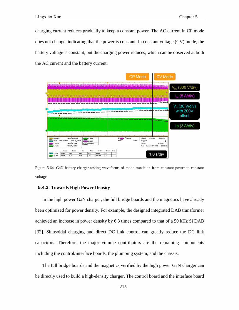
Lingxiao Xue Chapter 5
-215-
charging current reduces gradually to keep a constant power. The AC current in CP mode
does not change, indicating that the power is constant. In constant voltage (CV) mode, the
battery voltage is constant, but the charging power reduces, which can be observed at both
the AC current and the battery current.
Figure 5.64. GaN battery charger testing waveforms of mode transition from constant power to constant
voltage
5.4.3. Towards High Power Density
In the high power GaN charger, the full bridge boards and the magnetics have already
been optimized for power density. For example, the designed integrated DAB transformer
achieved an increase in power density by 6.3 times compared to that of a 50 kHz Si DAB
[32]. Sinusoidal charging and direct DC link control can greatly reduce the DC link
capacitors. Therefore, the major volume contributors are the remaining components
including the control/interface boards, the plumbing system, and the chassis.
The full bridge boards and the magnetics verified by the high power GaN charger can
be directly used to build a high-density charger. The control board and the interface board

Lingxiao Xue Chapter 5
-216-
can be shrunk with a customized design. A new cold plate and a new chassis were designed
by General Motor Company [35]. With careful mechanical designs, the power density is
projected to be 125 W/in3 [36]. The drawing of the high density charger is shown in Figure
5.65. This layout design gives a projection of how much GaN devices and sinusoidal
charging technique can improve the power density, but this prototype requires significant
effort on the design of customized DSP platform. Also, the construction and debugging of
the prototype are much more challenging in term of noise containment than the low density
ones, since its components are placed very close to each other. In this work, this prototype
is not built and tested, but it would be interesting to be explored in the future.
Figure 5.65. Drawing of the high-density GaN charger [35, 36]
5.5. SUMMARY AND CONCLUSION
This chapter demonstrated several design challenges of the GaN-based bi-directional
battery charger. The first section describes the driving channel and sensing circuit design
for the full bridge building block. An isolated DC/DC converter plus digital isolator scheme
was used to drive reliably the fast GaN modules. Adding filters into the full bridge can
improve the noise containment and reduce the interference to the control circuit. Special
1.8”PFC
DAB
Lingxiao Xue Chapter 5
-217-
attention should be paid to reduce the capacitive coupling between the isolation barriers.
Sensing circuits were designed to sense DC voltage, AC current and DC current of the full
bridge building block.
The totem-pole bridgeless PFC converter is promising for the application of GaN
devices. However, inherent challenges exist for this topology at the zero-crossing point of
AC voltage. Significantly different switching speeds of power devices exist from the high-
frequency phase leg and the low-frequency leg -- almost 100% and 0% duty cycle, which
abruptly changes around the zero-crossing. As a result, a current spike is usually observed
at the zero-crossing. This phenomenon becomes more severe with wide bandgap devices
at higher switching frequencies, with enlarged switching speed differences between two
legs, and reduced AC inductance values. This paper provided a detailed analysis for the
zero-crossing issue in two scenarios: transition delay of the low-frequency leg and
minimum pulse width limit of the high-frequency leg. A DSP-based digital modulator was
designed to address these two issues by applying lead time to the low-frequency leg and
digital dithering to increase equivalent resolution at the high-frequency leg. Some other
rules were also summarized to enable a robust modulator design, which is the main
challenge of this topology. Experimental results, based on a 500 kHz GaN converter
operating in continuous conduction mode, verified those methods. It was also noted that
using the duty cycle command instead of AC voltage to select the modulator mode resulted
in better dynamic performance. All these findings will aid in the implementation of wide
band gap devices in very high-frequency PFC circuits.
The dual active bridge converter is examined as the DC/DC stage of a battery charger
for the plug-in hybrid electric vehicle. The DAB design is challenging considering the wide

Lingxiao Xue Chapter 5
-218-
battery voltage range. If sinusoidal charging is implemented, the output current will
fluctuate at double line frequency, which furthers the difficulty of parameter selection. This
section investigates the DAB operating and switching conditions in great detail to account
for the cases of hard-switching, partial zero-voltage-switching and zero-voltage-switching,
based on which the DAB loss model is derived. The loss model was verified by
experimental measurement of a 500 kHz GaN DAB converter. With this DAB operating
and loss model, the DAB commutation inductance value is determined to achieve minimum
energy loss through the entire charging cycle. The decided inductance value is finally
integrated to a high-frequency transformer.
The overall charging system operation including bi-directional power flow and
charging profile control was verified on a GaN charger. Seamless bi-directional power flow
transition was demonstrated, and the charging mode transition from the constant power to
the constant voltage modes are also shown. To project the power density improvement, the
bulky cooling system, control/interface boards, and the chassis were re-designed. Together
with the proved building blocks including full bridges, magnetics and capacitors, a high-
density mock-up prototype with 125 W/in3 power density was assembled. It is shown that
with the implementation of GaN devices and DC link reduction techniques, and the
appropriate engineering effort on system packaging, a high power-density charger is very
possible.
5.6. LIST OF REFERENCES
[1] Z. Wei, H. Xiucheng, F. C. Lee, and L. Qiang, "Gate drive design considerations
for high voltage cascode GaN HEMT," in Proc. IEEE Appl. Power Electron. Conf.
Expo., 2014, pp. 1484-1489.
Lingxiao Xue Chapter 5
-219-
[2] Silicon Labs, "Isolator vs. Optocoupler Technology," [Online]. Available:
https://www.silabs.com/products/power/isolators/Pages/isolator-vs-optocoupler-
technology.aspx
[3] Texas Instruments, "ISO72x Single Channel High-Speed Digital Isolators," Rep.
no. ISO72x, Datasheet., 2015. Accessed on Aug. 30, 2015.
[4] Avago Technologies, "HCPL-9000 High Speed Digital Isolators," Rep. no. HCPL-
9000, Datasheet., 2013. Accessed on Aug. 30, 2015.
[5] C. Kitchin and L. Counts, "A designer's guide to instrumentation amplifiers," 2006.
[Online]. Available: http://www.analog.com/media/en/training-seminars/design-
handbooks/5812756674312778737Complete_In_Amp.pdf
[6] X. Lingxiao, S. Zhiyu, M. Mingkai, D. Boroyevich, R. Burgos, B. Hughes, et al.,
"Bi-directional PHEV battery charger based on normally-off GaN-on-Si multi-chip
module," in Proc. IEEE Appl. Power Electron. Conf. Expo., 2014, pp. 1662-1668.
[7] L. Huber, J. Yungtaek, and M. M. Jovanovic, "Performance Evaluation of
Bridgeless PFC Boost Rectifiers," IEEE Trans. Power Electron., vol. 23, no. 3, pp.
1381-1390, 2008.
[8] K. Pengju, W. Shuo, and F. C. Lee, "Common Mode EMI Noise Suppression for
Bridgeless PFC Converters," IEEE Trans. Power Electron., vol. 23, no. 1, pp. 291-
297, 2008.
[9] Y. Jang and M. M. Jovanovic, "A bridgeless PFC boost rectifier with optimized
magnetic utilization," IEEE Trans. Power Electron., vol. 24, no. 1, pp. 85-93, 2009.
[10] S. Bin, Z. Junming, and L. Zhengyu, "Totem-Pole Boost Bridgeless PFC Rectifier
With Simple Zero-Current Detection and Full-Range ZVS Operating at the
Boundary of DCM/CCM," IEEE Trans. Power Electron., vol. 26, no. 2, pp. 427-
435, 2011.
[11] E. Firmansyah, S. Tomioka, S. Abe, M. Shoyama, and T. Ninomiya, "Totem-Pole
Power-Factor-Correction Converter under Critical-Conduction-Mode Interleaved
Operation," IEICE Trans. Commun., vol. E93-B, no. 9, pp. 2250-2256, 2010.
[12] C. Marxgut, F. Krismer, D. Bortis, and J. W. Kolar, "Ultraflat Interleaved
Triangular Current Mode (TCM) Single-Phase PFC Rectifier," IEEE Trans. Power
Electron., vol. 29, no. 2, pp. 873-882, 2014.
[13] Z. Liang, W. Yi-Feng, and M. Umesh, "True Bridgeless Totem-pole PFC based on
GaN HEMTs," in Proc. PCIM Eur., 2013, pp. 1017-1022.
[14] Z. Liu, X. Huang, M. Mu, Y. Yang, F. C. Lee, and Q. Li, "Design and evaluation
of GaN-based dual-phase interleaved MHz critical mode PFC converter," in Proc.
IEEE Energy Convers. Congr. Expo., 2014, pp. 611-616.
[15] E. Firmansyah, S. Tomioka, A. Seiya, M. Shoyama, and T. Ninomiya, "Totem-Pole
Power-Factor-Correction Converter under Critical-Conduction-Mode Interleaved
Operation," IEICE Trans. Commun., vol. 93, no. 9, pp. 2250-2256, 2010.
[16] J. C. Salmon, "Techniques for minimizing the input current distortion of current-
controlled single-phase boost rectifiers," IEEE Trans. Power Electron., vol. 8, no.
4, pp. 509-520, 1993.
[17] J. Sun, "On the zero-crossing distortion in single-phase PFC converters," IEEE
Trans. Power Electron., vol. 19, no. 3, pp. 685-692, 2004.
Lingxiao Xue Chapter 5
-220-
[18] K. De Gusseme, D. M. Van de Sype, W. R. Ryckaert, V. A. De Vleeschauwer, and
J. A. Melkebeek, "Zero-crossing distortion in grid-coupled AC-DC converters," in
Proc. Eur. Conf. Power Electron. Appl., 2005, pp. 10 pp.-P.10.
[19] D. Paschedag and M. Ferdowsi, "Elimination of zero-crossing distortion in a power
factor correction circuit," in Proc. IEEE Energy Convers. Congr. Expo., 2012, pp.
4049-4052.
[20] L. Yu-Kang, O. Sheng-Yuan, and C. Huang-Jen, "On evaluating the current
distortion of the single-phase switch-mode rectifiers with current slope maps,"
IEEE Trans. Ind. Electron., vol. 49, no. 5, pp. 1128-1137, 2002.
[21] Q. Xiaohui and R. Xinbo, "A Scheme for Improving Input Current Zero-Crossing
Distortion of Single-Phase Power-Factor-Correction Converters," in Proc. IEEE
Power Electron. Specialists Conf., 2006, pp. 1-6.
[22] T. Instrument, "TMS320x2834x Delfino Enhanced Pulse Width Modulator (ePWM)
Module," 2009.
[23] R. W. A. A. De Doncker, D. M. Divan, and M. H. Kheraluwala, "A three-phase
soft-switched high-power-density DC/DC converter for high-power applications,"
IEEE Trans. Ind. Appl. vol. 27, no. 1, pp. 63-73, 1991.
[24] F. Krismer and J. W. Kolar, "Closed Form Solution for Minimum Conduction Loss
Modulation of DAB Converters," IEEE Trans. Power Electron., vol. 27, no. 1, pp.
174-188, 2012.
[25] G. G. Oggier, R. Ledhold, G. O. Garcia, A. R. Oliva, J. C. Balda, and F. Barlow,
"Extending the ZVS Operating Range of Dual Active Bridge High-Power DC-DC
Converters," in Proc. IEEE Power Electron. Specialists Conf., 2006, pp. 1-7.
[26] J. Everts, F. Krismer, J. Van den Keybus, J. Driesen, and J. W. Kolar, "Optimal
ZVS Modulation of Single-Phase Single-Stage Bidirectional DAB
AC–DC Converters," IEEE Trans. Power Electron., vol. 29, no. 8, pp.
3954-3970, 2014.
[27] M. N. Kheraluwala, R. W. Gascoigne, D. M. Divan, and E. D. Baumann,
"Performance characterization of a high-power dual active bridge," IEEE Trans.
Ind. Appl., vol. 28, no. 6, pp. 1294-1301, 1992.
[28] L. Jin, C. Zheng, S. Zhiyu, P. Mattavelli, L. Jinjun, and D. Boroyevich, "An
adaptive dead-time control scheme for high-switching-frequency dual-active-
bridge converter," in Proc. IEEE Appl. Power Electron. Conf. Expo., 2012, pp.
1355-1361.
[29] R. Elferich, "General ZVS half bridge model regarding nonlinear capacitances and
application to LLC design," in Proc. IEEE Energy Convers. Congr. Expo., 2012,
pp. 4404-4410.
[30] M. Mingkai, L. Qiang, D. J. Gilham, F. C. Lee, and K. D. T. Ngo, "New Core Loss
Measurement Method for High-Frequency Magnetic Materials," Power Electronics,
IEEE Transactions on, vol. 29, no. 8, pp. 4374-4381, 2014.
[31] X. Lingxiao, M. Mingkai, D. Boroyevich, and P. Mattavelli, "The optimal design
of GaN-based Dual Active Bridge for bi-directional Plug-IN Hybrid Electric
Vehicle (PHEV) charger," in Proc. IEEE Appl. Power Electron. Conf. Expo., 2015,
pp. 602-608.
Lingxiao Xue Chapter 5
-221-
[32] M. Mu, L. Xue, D. Boroyevich, and P. Mattavelli, "Design of Integrated
Transformer and Inductor for High Frequency Dual Active Bridge GaN Charger
for PHEV," Proc. IEEE Appl. Power Electron. Conf. Expo., 2015. pp. 579-585
[33] X. Lingxiao, P. Mattavelli, D. Boroyevich, S. Zhiyu, and R. Burgos, "Closed-loop
control on DC link voltage ripple of plug-in hybrid electric vehicle charger with
sinusoidal charging," in Proc. IEEE Energy Convers. Congr. Expo., 2013 IEEE,
2013, pp. 3607-3614.
[34] X. Lingxiao, D. Diaz, S. Zhiyu, L. Fang, P. Mattavelli, and D. Boroyevich, "Dual
active bridge based battery charger for plug-in hybrid electric vehicle with charging
current containing low frequency ripple," in Proc. IEEE Appl. Power Electron.
Conf. Expo., 2013, pp. 1920-1925.
[35] "Gallium-Nitride Switch Technology for Bi-directional Battery-to-Grid Charger
Applications," Arpa-E ADEPT Project Report. Awards number: DE-AR-0000117,
2014.
[36] B. Hughes. Normally-Off GaN-on-Si Bi-Directional Automobile Battery-to -Grid
6.6kW Charger Switching at 500kHz. presented at 2014 Appl. Power Electron.
Conf. Expo. [Online]. Available: http://www.apec-conf.org/wp-
content/uploads/IS2-4-5.pdf

Lingxiao Xue Chapter 6
-222-
Chapter 6. CONCLUSION AND FUTURE WORK
6.1. SUMMARY AND CONCLUSIONS
This work explores how GaN devices, advanced control can improve the power density
of battery chargers for the plug-in hybrid electric vehicle. A literature review revealed that
the current design solutions are all low in power density due to the limitation of silicon
devices and big DC link capacitors. Two factors were then identified that could improve
the power density of the charger while maintaining a high efficiency, namely, the
implementation of wide band-gap devices, and the development of DC link reduction
techniques.
This dissertation started with the characterization of one of the most promising wide
band-gap devices for this application, the gallium nitride high electronic mobility transistor
(GaN HEMT). A multi-chip-module (MCM) approach was used to integrate multiple GaN
transistors into a package that enables fast, reliable, and efficient switching. The static
characterization results show that the 600 V, 30 A GaN module is superior to its silicon
counterparts in terms of on-resistance, output charge, and reverse recovery charge. The
switching characterization shows that the GaN MCM can switch very fast with over 100
V/s slew rate. This high switching speed enables low switching loss that has been verified
in a 500 kHz hard-switching boost converter. The peak efficiency achieved was 97.5%. A
loss model is derived based on the characterization results and shows a good match with
the measurement results.
To find the best topology suitable to the charger application and the high-speed GaN
devices, a topology selection of AC/DC converters was conducted. The two-stage solution

Lingxiao Xue Chapter 6
-223-
that cascades a non-isolated AC/DC converter and an isolated DC/DC converter turns out
to be most promising. For both stages, converter topologies built with phase-legs whose
terminal voltages can be clamped are strongly preferred. Other topologies may not
effectively reduce the parasitic inductances of the switching loop, causing high ringing
voltages due to fast switching speed, which may damage the GaN devices. The selection
of topologies must consider efficiency, power density, and realization complexity. To
achieve best balance of those criteria, the full bridge AC/DC plus dual active bridge DC/DC
topology was selected for this application with the investigated GaN modules.
The DC link capacitor occupies a large portion of the total volume, even if other passive
components can be significantly shrunk by using the GaN switching technology, mainly
because its size is determined by the double-line frequency instead of the switching
frequency. This work proposed different charging schemes to reduce the DC link
capacitance by balancing the ripple power from input and output. An in-depth analysis on
ripple power balance, with converter loss considered, provided the conditions to eliminate
the low-frequency DC link capacitors. However, the resultant sinusoidal charging scheme
caused high converter loss due to hard-switching. The charging current is thereby changed
to a PWM waveform at the double-line frequency, and by periodically turning off the
DC/DC stage, 39% of the converter loss can be saved.
When the GaN-based bi-directional charger was built, some practical design issues at
different levels of implementation were outlined and solved. For the full bridge building
block, special effort was spent on the reliable driving and sensing circuitry design. It was
found that the driving scheme, part selection, layout, and placement position of sensors are
all critical for a successful realization of functions. The design of the AC/DC stage stressed

Lingxiao Xue Chapter 6
-224-
modulator improvement to solve the issues of current spike at the zero-crossing of the line
voltage for high frequency totem-pole bridgeless converters. One of the major challenges
of the DAB DC/DC converter design is understanding converter loss, especially when
hard-switching and partial zero-voltage-switching are present. This work provided
analytical expressions to model the converter loss at various operating conditions, which
gave good match with the measurement results.
The overall charging system operation including the seamless transition of bi-
directional power flow and the charging profile control was verified on a GaN charger
prototype. To project the power density improvement, some bulky components were re-
designed. Together with the proved building blocks including full bridges, magnetics and
capacitors, a high-density mock-up prototype with 125 W/in3 power density was assembled.
6.2. FUTURE WORK
GaN transistors enable unprecedented high switching speed. On one hand, this enables
low switching loss, high switching frequency, and high power density. On the other hand,
there are two important issues that must be considered along with the benefits. First, how
to achieve reliable driving to fully unleash the switching speed of the GaN transistors. In
this work, the localized driving and switching loop has very low parasitic inductances. A
zero-ohm gate resistor still leads to too high voltage overshoot. Therefore, the GaN
transistors are slow down for safe operation by adding external gate resistors in a similar
fashion as in some other reported work. In the future, a monolithic solution reached by
integrating the GaN and its driving circuits at the semiconductor level can almost eliminate
the inductances, so the switching speed of the GaN devices can be fully used.

Lingxiao Xue Chapter 6
-225-
Secondly, the high switching speed causes severe electromagnetic interference (EMI)
due to very steep voltage transition edges and rich harmonics. This work provided some
practical solutions to suppress and locally confine those noises from interfering with the
sensitive circuit. However, future work should consider how to model and quantify the
noise source (GaN hard-switching and soft-switching), the new noise propagation path
(discrete or module packages), and identify other noise victims. This could be extremely
important for the future adoption of GaN.
This paper proposed pulse charging for the traction lithium-ion batteries. Although
some papers have already show that the lithium-ion battery can be charged with high-
frequency current, which poses negligible adverse or even some beneficial impact on the
battery in the short term, a more focused and in-depth investigation on the long term effect
is necessary.
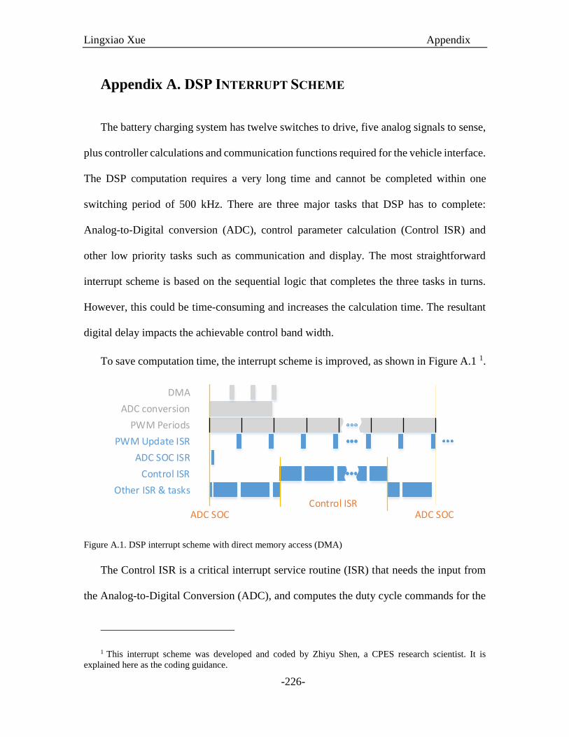
Lingxiao Xue Appendix
-226-
Appendix A. DSP INTERRUPT SCHEME
The battery charging system has twelve switches to drive, five analog signals to sense,
plus controller calculations and communication functions required for the vehicle interface.
The DSP computation requires a very long time and cannot be completed within one
switching period of 500 kHz. There are three major tasks that DSP has to complete:
Analog-to-Digital conversion (ADC), control parameter calculation (Control ISR) and
other low priority tasks such as communication and display. The most straightforward
interrupt scheme is based on the sequential logic that completes the three tasks in turns.
However, this could be time-consuming and increases the calculation time. The resultant
digital delay impacts the achievable control band width.
To save computation time, the interrupt scheme is improved, as shown in Figure A.1 1.
ADC conversion
PWM Periods
PWM Update ISR
Control ISR
Other ISR & tasks
ADC SOC
DMA
ADC SOC
ADC SOC ISR
Control ISR
Figure A.1. DSP interrupt scheme with direct memory access (DMA)
The Control ISR is a critical interrupt service routine (ISR) that needs the input from
the Analog-to-Digital Conversion (ADC), and computes the duty cycle commands for the
1 This interrupt scheme was developed and coded by Zhiyu Shen, a CPES research scientist. It is
explained here as the coding guidance.

Lingxiao Xue Appendix
-227-
next cycle. Other ISR & tasks include communication and display, which have low update
frequency; therefore, it is less sensitive to timing and can be conducted in parallel with the
ADC conversion. Therefore, the improved interrupt scheme lets ADC conversion start and
uses direct memory access (DMA) module to monitor the conversion and read the data.
The DMA module will generate an interrupt once the ADC data are ready to use for the
calculation, so this interrupt is used to start the control ISR. During the ADC conversion,
those less important tasks can be conducted in parallel.
With the improved interrupt scheme, the DSP calculation can be finished within 20 µs.
Therefore the sampling frequency is selected as 50 kHz. Note that the switching frequency
is 500 kHz and the switching period is two µs. This means that in every control cycle, we
need to calculate duty cycle commands for the next ten switching cycle. This offers the
possibility of digital dithering to improve PWM resolution, as explained in Section 5.2.4.3.
However, the control delay related to the 50 kHz sampling frequency reduces the
achievable bandwidth, even though the switching frequency is ten times.
To assign different duty cycle numbers for the ten switching cycles, as required by the
digital dithering scheme, a separate interrupt (PWM update ISR in Figure A.1) is used to
update the PWM registers every switching period. This ISR program needs to be very
efficient in CPU cycles, as it will be multiplied by ten and occupy many CPU resources in
one sample period.

Lingxiao Xue Appendix
-228-
Appendix B. VEHICLE INTERFACE AND CHARGING CONTROL
The onboard battery charger should accept commands from the vehicle and send the
key battery and charger information back to the vehicle. The vehicle side command will
set the current limit of the AC input to the battery charger. This is important also because,
during the discharging mode, the same command can control the amount of energy drained
from the battery pack. However, the battery charger should also protect the battery from
being charged or discharged with excessive currents. The DSP platform should
accommodate those needs.
The charging control is shown in Figure B.1. Because the AC voltage is fixed by the
grid, the AC current that is sunk or sourced by the charger determines the power delivered
to or from the battery. This AC current command is given by the vehicle computer, but can
be overridden by the battery side if the resultant charging or discharging current is too high.
If the AC current command (Iac_cmd) is not causing battery over-current, this command
will be taken as the reference of the AC current (Iac_ref). This case is illustrated in Figure B.
1(a). The real AC current will finally follow this reference because of the regulation effect
of the AC current controller. The “extra” battery power is reflected by the difference
between the AC current reference and the output of the DC voltage controller. This
difference is scaled and subtracted from the battery current limit, so the battery current is
consequently reduced. This process will continue and is finally stabilized at a point where
the power balance is satisfied. The DC bus voltage controller plays the important role of
keeping power balance.
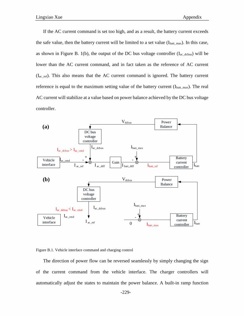
Lingxiao Xue Appendix
-229-
If the AC current command is set too high, and as a result, the battery current exceeds
the safe value, then the battery current will be limited to a set value (Ibatt_max). In this case,
as shown in Figure B. 1(b), the output of the DC bus voltage controller (Iac_dcbus) will be
lower than the AC current command, and in fact taken as the reference of AC current
(Iac_ref). This also means that the AC current command is ignored. The battery current
reference is equal to the maximum setting value of the battery current (Ibatt_max). The real
AC current will stabilize at a value based on power balance achieved by the DC bus voltage
controller.
DC bus
voltage
controller
Vehicle
interface
Iac_cmd -+
Iac_dcbus
Power
Balance
Gain
Battery
current
controllerIbattI ac_ref
Vdcbus
Iac_dcbus > Iac_cmd
DC bus
voltage
controller
Vehicle
interface
Iac_cmd
Power
Balance
Battery
current
controllerIbatt
I ac_ref
Vdcbus
Iac_dcbusIac_dcbus < Iac_cmd
(a)
(b)
Ibatt_ref
Ibatt_max
I ac_diff I batt_diff
Ibatt_max
0
Ibatt_max
-+
-+
Figure B.1. Vehicle interface command and charging control
The direction of power flow can be reversed seamlessly by simply changing the sign
of the current command from the vehicle interface. The charger controllers will
automatically adjust the states to maintain the power balance. A built-in ramp function
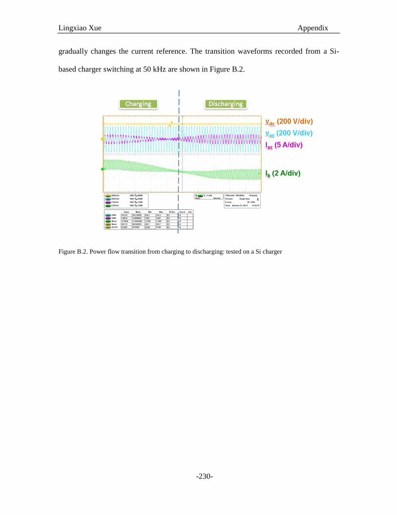
Lingxiao Xue Appendix
-230-
gradually changes the current reference. The transition waveforms recorded from a Si-
based charger switching at 50 kHz are shown in Figure B.2.
Figure B.2. Power flow transition from charging to discharging: tested on a Si charger