a hexagonal array machine for concurrent …web.eecs.umich.edu/~mazum/papers-mazum/ham.pdfa...
TRANSCRIPT

A Hexagonal Array Machine for Concurrent Multilayer Maze Routing
by R. Venkateswaran and P. Mazumder
In the late 80’s, the network of workstations (having a clock rate of about 30 MHz) became the de facto CAD design environment and replaced the mid-frame Vax machines. Our research vision was to develop distributed layout synthesis tools where coarse-grained tasks such as cell placement, floorplanning, compaction and chip testing problems were solved by using Genetic Algorithms by running concurrently over multiple desktop computers. See our book on Genetic Algorithms for details. However, chip routing algorithms require fine-grained parallelism. That is why, we designed two co-processor chips: HAM and CHiRPS. They were designed and fabricated by us at that time to solve the emerging crisis of layout turnaround time due to aggressive scaling of VLSI chips.. However, in 1992 DEC alpha chips leapfrogged the clocking rate in the regime of 300 MHz by taking adavntages of several breakthroughs in CMOS process technology and subsequently Intel, which acquired DEC foundry in mid 90’s, made further advancements in process technology and ramped the clock speed to 3 GHz. This technological breakthrough had mitigated the needs for parallel CAD and the routing coprocessors we built at that time. Hexagonal Array Machine was designed and tested by R. Venketswaran and P. Mazumder in 1990. HAM coprocessor was later replaced by them by designing a general purpose multilayer routing chip that was named: Configurable Highly Routable Parallel System (CHiRPS). Please find the description of CHiRPS coprocessor in an accompanying paper that demonstrates how fast parallel routing can be achieved by polymorphic switch setting in the massively parallel ensemble of rudimentary processing elements in CHiRPS. The programmable coprocessor provided fast and efficient results for different styles of routing such as maze, line probe, channel, switchbox, general area, and so on
.
IEEE TRANSACTIONS ON VERY LARGE SCALE INTEGRATION (VLSI) SYSTEMS, VOL. 1, NO. I , MARCH 1993 31
Coprocessor Design for Multilayer Surface-Mounted PCB Routing
Ramachandran Venkateswaran, Student Member, IEEE, and Pinaki Mazumder, Member, IEEE
Absfract-The printed circuit boards (PCB’s) for the 1990’s can be characterized by higher circuit densities, multiple routing layers, newer packaging technologies, and demand for lower manufacturing costs. The task of connecting all the traces on such a complex board will become more and more time con- suming. This paper presents the issues involved in the design of a special-purpose processing array system, called HAM, which will accelerate such compute-intensive wire routing tasks. It is especially suited for double-sided surface-mounted boards which require complex three-dimensional search operations over multiple wiring planes. The novel features of the design include a hexagonal interconnection scheme to improve workload dis- tributions during multilayer concurrent search operations and the VLSI custom design of the processors. Particular emphasis has been placed on the demands of maze routing such as in the allocation of the routing database on the multiple processors, design of buffer stores for maintaining the frontier-lists, etc. A novel scheme of cell-address propagation, which is quite differ- ent from the traditional grid-coordinate approach is discussed. This provides for rapid lookup of pertinent routing information and can be extended to any distributed memory multiprocessor system. A global pipelining scheme of cell updates and expands is discussed. Experimental results are presented relating the speedup to Merent criteria such as number of processors and size of the local memory for two different modes of parallel wave propagation.
I. INTRODUCTION HE NEW generation printed circuit boards (PCB’s) can T be characterized by higher circuit densities, finer trace
widths, multiple routing layers, stringent performance con- straints, complex packaging and manufacturing technology, and demand for lower manufacturing costs. Designers must get their products to the market fast or risk losing their competitive edge. This requires an integrated design solution uniting the power and convenience of automated tools with the interactive expertise of the designer. Several cost measures are often used in the routing process. For instance, nets pertaining to analog components such as op-amps need to be routed within a certain pre-specified length. Board manufacturability and ease of update are important routing requirements. Vias have to be intelligently used to provide compact multilayer routes for all the nets. Wirelength minimization is also important for min-
Manuscript received May 4, 1992; revised August 25, 1992 and October 27, 1992. This work was supported in part by an IBM graduate fellowship, by the U. S. Army Research Office under the URI program Grant DAAL 03- 87-K-0007, by the Office of Naval Research under Grant 00 014-85-K-0122, and by the National Science Foundation under Grant 9013092.
The authors are with the Department of Electrical Engineering and Com- puter Science, The University of Michigan, Ann Arbor, MI 48109-2122.
IEEE Log Number 9206233.
Blind Signal layer 1
layer 2
layer 3
layer4
layer 5
I Y layer 6
Spin1
”vgb bo*
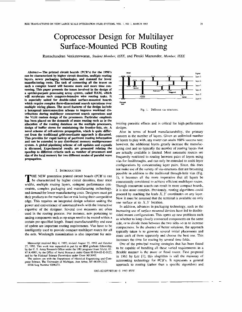
Fig. I . Different via structures.
imizing parasitic effects and is critical for high-performance designs.
Also in terms of board manufacturability, the primary concem is the number of layers. Given an unlimited number of layers to play with, any router can attain 100% success rate; however, the additional layers greatly increase the manufac- turing cost and so typically the number of routing layers that are actually available is limited. Most automatic routers are frequently restricted to routing between pairs of layers using vias for feedthroughs, and can only be extended to multi-layer configurations by concatenating layer pairs. Since, this does not make use of the variety of via-structures that are becoming possible in addition to the traditional through-hole vias (Fig. l), it becomes all the more imperative that all layers be concurrently considered to achieve efficient multilayer routes. Though concurrent search can result in more compact boards, it is also more complex. Previously, routing algorithms could proceed by reaching the leads X , Y coordinates on any layer. Now it must be assumed that the terminal is available on only one surface at its X , Y location.
In addition, advances in packaging technology, such as the increasing use of sur$ace mounted devices have led to double- sided mount configurations. This opens up new problems such as whether to keep closely connected components on the same side, or to divide them between the two sides so as to increase compactness. In the absence of better solutions, the approach typically taken is to generate several initial placements and route each of them separately and choose the best one. This increases the time for routing by several time folds.
One of the principal routing strategies that has been found to be capable of handling all these varied requirements in a flexible manner is the maze or flood router. First proposed in 1961 by Lee [l] , this alogrithm is still the mainstay of autorouting technology for PCB’s. It represents a general approach to routing (rather than a specific algorithm) and
1063-8210/93$03.00 0 1993 IEEE
1

32 IEEE TRANSACTIONS ON VERY LARGE SCALE INTEGRATION (VLSI) SYSTEMS, VOL. 1 , NO. I , MARCH 1993
further guarantees to find a path if one exists. The maze router can be extended for multilayer cases as well. However, it is computationally extremely expensive. One simplification is to first use faster approaches such as pattern routing to complete most of the easy connections which account for about 85% of all the nets. Unfortunately, though, the last 10-15% of all traces require the most time and computing resources since they are often the most complex to route. It may also become necessary to rip-up and reroute existing connections to make way for these traces. This process typically requires three or four invocations of the Lee algorithm. Since the Lee algorithm is at its slowest when connections are not found, the speed problem becomes significant. Furthermore, it gets only more worse as this phase is often done interactively with expert designer interface and hence rapid response times are desirable.
A custom-hardware implementation for maze routing can run as much as a thousand times faster than a general purpose computer if the routing processor architecture is ingeniously designed to exploit all the intrinsic data parallelism in the search operations. Hardware costs are rapidly decreasing and with the aid of VLSI it is now possible to construct a single- board hardware accelerator that can interface to a personal computer or workstation running routing software. Further- more, it is unlikely that the maze routing paradigm can be supplemented in the near future by any other because of its extreme flexibility, and because of the nonplanar nature of grids in complex multilayer PCB’s. Thus a routing processor supporting the general maze router with flexible cost capability does not suffer the risk of obsolescence as could be the case with other algorithm-specific solutions. This paper focuses on the practical issues in the actual construction of one such system, called Hexagonal Array Machine and acronymed as (HAM). Since multidimensional arrays are very difficult to implement, and since the sizes of the grids are not known a priori. HAM maps the grid onto a smaller number of pro- cessors connected in a hexagonal wraparound topology. The hexagonal interconnection scheme has been previously shown [2], to possess the best characteristics amongst other two- dimensional topologies for multilayer concurrent searching operations.
The rest of the paper is organized as follows. In Section 11, we present a motivation for our work and summarize some of the previous work done. Section 111 describes the overall architecture and some issues pertaining to maze routing. A new and more practical scheme for address computation during wavefront propagation is presented. Section IV describes the VLSI design issues for the construction of the individual HAM processors. Issues such as memory and buffer storage organization, datapath and microprogrammed control are dis- cussed. The timing and instruction flow is described along with a critical path analysis. In Section V, we summarize the results of system level simulations which evaluate the effect of internal storage size, number of processors and mode of wavefront expansion (one wavefront or multiple wavefronts at a time) on overall performance. It may be noted that the distributed nature of computation proposed here is also applicable to other implementations as well.
(a) (b)
routing solution. Fig. 2. (a) A small double-sided SMT routing problem (b) The three-layer
11. MULTILAYER CONCURRENT MAZE-ROUTING
A. Maze Routing
Maze routing is usually the only practical solution to do multilayer routing with double-sided surface mounted module placement. Maze routing consists of three main operations: the first prepares the board for routing by partitioning it into hundreds or thousands of cells. The size of the grid cells is determined by the pad spacing and other design rules being employed. All the structures on the board such as pads, copper areas, traces, tooling holes, etc. are marked in the cells to which they belong. After creating the grid, the maze router begins an “expansion” stage. The router examines all the grid points in larger and larger concentric rings around the source pad till the destination is reached. Simultaneously, the router assigns cost values to each cell in accordance to some metric. These metrics are based on a variety of routing variables such as heading toward the target, adding a via, making a comer, or using preferred routing layers. In fact, the popularity of the maze router stems from the capability to tailer the cost functions to meet almost any routing requirements. Once the target pad is reached a “backtrace” is performed to the origin pad from the target point along one of the lowest cost paths.
B. Need for Concurrent Multilayer Search One reason for multilayer search as was mentioned earlier
is to minimize the total number of layers, thereby reducing the manufacturing costs of the board. The problem is more severe in double-sided surface-mounted PCB’s with multiple signal layers. For example, consider a three-layer SMT board with three modules Cl,C2, and C3 as shown in Fig. 2(a). Nets A and B represent interconnections between terminals on one side of the board while net C interconnects two terminals on the other side of the board. Net D, on the other hand, connects two pins on opposite sides. An optimal shortest path routing solution is shown in Fig. 2(b). Note the buried vias for net B, which allows net C to be routed beneath its terminals, could be readily found only by using concurrent search on all layers.

VENKATESWARAN AND MAZUMDER: DESIGN FOR SURFACE-MOUNTED PCB ROUTING 33
TABLE I SOME EXISTING ROUTING ACCELERATORS
Accelerator Architecture Routing Model Comments
Wire Routing Machine [7] 32 x 32 array with General purpose 280 pproc Maze routing for 1-2 layer grids with
Interconnection Network PE design
endaround rowlcolumn + 15Kh mednode detailedglobal wiring variable grid weighting wraparounds
Distributed Array 64 x 64 array with global Bit-serial proc with Maze routing for 2-layers unit cost grids; Processor [8] rowkol buses for global memory detailedglobal wiring DAP is a commercial
Toroidal Machine [9] movement machine Prototype 8 x 8 array with twisted torus wraparounds ROM and RAM detailedglobal wiring support for interactive
MANURE2 [4] SISD microcode machine Custom designed bitmap + Maze routing for detailed Multilayer support by
NEC ~ P D 7 8 0 0 PE + 8Kb Maze routing for 1-2 layers weighted grids;
rip-up and reroute
address + markkost wiring reconfiguring via-bits in processors bitmap; support for diagonal
routing; staged expansions
C. Previous Accelerators
Routing accelerators can be broadly categorized as either SISD (single instruction single data) or SIMD (single in- struction multiple data) machines. The first category [4]-[6] consists of a conventional processor aided by special-purpose support hardware to speed up some of the computations in- volved such as address computations, frontier-list managment, etc. However, they do not capture the parallelism inherent within the algorithm. Instead, speedup is obtained by the elimination of operating system overheads and by efficiently performing some of the common operations in hardware.
The SIMD systems account for the intrinsic data parallelism in maze routing. The primary idea is to use an N x N array of identical processing elements that have a one-to-one correspondence with the N x N grid plane and so achieve a linear runtime for finding a path. A major disadvantage with such “full-grid” machines is that they need O ( N 2 ) PE’s despite the fact that almost all of them are not utilized at the same time. Moreover, they cannot handle problem sizes which are bigger than the physical size of the processing array. This is solved by allowing for wraparound connections and making each PE in the array to be responsible for maintaining the status of several grid cells. Some of the designs which fall in this category are the Wire Routing Machine [7], the Distributed Array Processor [8], and the Toroidal Machine [9]. A brief comparison of these routers is provided in Table I.
The HAM approach is also SIMD based. It improves on existing approaches in three main aspects. a) The individual compute elements have been custom designed keeping in mind the nature of data retrieval and manipulation operations re- quired for maze routing. Careful consideration has been given to the interprocessor communication demands which is often the bottleneck for previous routers. b) The second reason has to do with the mapping used to assign grid cells to processors so that the workload gets uniformly distributed. The mapping provides the maximum interprocessor cycle period, i.e., the minimum distance between two occurrences of the same processing element along any straight line (including diagonal lines) [ 2 ] . c) The hexagonal interconnection which supports concurrent search in multiple layers needed in complex board routing.
(plug-in accelerator board)
pTf 0 0
Fig. 3. Overview of the HAM routing system.
111. HAM SYSTEM ARCHITECTURE
A. General Organization
In this section, we present the overall system organization. There are three levels of interfaces involved. The first deals with the external interface between the workstation and the accelerator. The second deals with the interface between the accelerator controller and the processors in the array and the third level is the one between the processors themselves.
External Interface: Fig. 3 shows the HAM system organi- zation in a distributed CAD system running on a network of workstations. It is conceived of as a single board system that can be plugged into an expansion slot of any conventional workstation running CAD software. The layout software can therefore address the accelerator as a device whenever it needs to perform a maze routing operaton. Processors are organized in a two-dimensional lattice. The processor array operates under the supervision of a global control unit (GCU) which is responsible for interfacing with the host workstation, for performing the sequential parts of the algorithm and for issuing the commands which are performed by all processors in a lock-step fashion.

34
STATUS OMASK
IEEE TRANSACTIONS ON VERY LARGE SCALE INTEGRATION (VLSI) SYSTEMS, VOL. 1. NO. 1, MARCH 1993
COST E W N S U D
to wkhborlng PES
Fig. 4. Interprocessor communication interface.
GCU/Array Interface: The HAM system is based on an SIMD model, wherein each processor basically executes the same instruction in the same clock cycle on its local data set. In each cycle, the GCU broadcasts an address to all processors which corresponds to a particular instruction stored in the processor’s control memory. The processors themselves lack any decision making capability. Sample instructions in- clude expand i n direction d , backtrace, start a new wave- f ront and so on. In addition, the GCU has access to the input and output ports of the processors so as to be able to perform initialization and obtain results in the end.
Interprocessor Interface: Maze routing is highly commu- nication intensive, but the communications follow a near- neighbor pattern. Consequently, each processor is directly connected to six other nodes in the array. Communication is allowed only on these links. In particular, there is no message- passing mechanism between any two arbitrary processors in the array. This model therefore eliminates the need for any hardware message router. Also, the proposed system is based on a distributed memory model. Any changes to the memory contents is to be accomplished by message passing alone. This eliminates the need for complex data consistency and data coherency control present in a shared- memory system. In an ideal system, each processor will have six parallel ports to communicate with the six neighbors; but in our implementation we have opted for a single-port time-multiplexed scheme, wherein, in any one clock cycle, all processors in the array talk to their neighbor in one of the six directions. A multiplexer is placed at the input pins to select one of the 6 neighbor data, as shown in Fig. 4. This selection is based on the dir control bits generated by the processor.
B. Maze Routing Requirements
In the HAM system, as presented above, each processor has access only to its local memory, called grid memory, which stores the information pertaining to all the cells that are mapped onto that processor. In this paper, the per-cell storage format used is shown in Fig. 5. The cost field stores the least cost path discovered to that cell from the source cell. The directional mask field is used for backtracing the net from the target cell to the source. The content of the status field is as shown in the figure and is used to control the wave propagation and backtrace phases.
18 15 9 0
Fig. 5. Information stored in grid-memory for each grid cell.
During the maze algorithm, the processors constantly have to access their local stores and exchange information be- tween themselves through message-passing. This raises several interesting questions that become critical in determining per- formance.
1) How does one processor inform the other as to the
2) What is the message overhead during wave-propagation? 3) How do wavefronts proceed? 4) How do the processors keep track of the frontier list (i.e.,
cells that have been reached during wave propagation but which have not yet been expanded out)?
1) Next-Cell Address Computation: Suppose two neighbor- ing grid cells c1 and cz are mapped to processors pl and p:! and their information is stored at addresses ml and mz in the respective local memories. Then, in the traditional grid- coordinate transfer scheme, pl communicates the ( x , y, z) grid coordinates of cz to pz; which lacking other information has to search, possibly its entire memory, trying to determine the location (mz) where data for cz is to be stored. In [2] we had alluded to this problem and had suggested that it would be much faster to have pl communicate m2 directly to pz. This is the basis of our address-transfer scheme. The message size for the address-transfer scheme is only [log[(kG,G,)/N]1 bits for a k-layer G, x G, grid mapped onto an N-processor system. As opposed to this, transferring coordinates needs [(log k + log G, + log G,)]. Thus there is also a saving in the message traffic.
The problem, therefore, is reduced to one of each processor determining the address to transmit to their neighbors in all six directions. An index-based mapping scheme was given an earlier paper [2] and is briefly summarized below. “Let c 1 . CZ, . . . , ck be the ordered list of cells to which processor p is assigned. The ordering is by a row-major traversal of cells one layer at a time. Then, we define INDEX[c;] = i . Once, all the INDEX values are known, each processing element can calculate the difference Ad, between its INDEX value and the INDEX values of its neighbor in direction d . Grid boundaries can be handled using a dummy value X.” Furthermore, it was shown that for the hexagonal mapping on N processors, the maximum absolute value of Ad is [max(G,G,)/Nl, independent of the number of layers k.
Thus in this scheme, the entry for cell (2, y, z) is stored in the local memory of the mapped processing element at address (zk . . . zo, b, . . . bo) where Zk . . . zo is the binary representation of z and b, . . . bo is the binary representation of INDEX
identity of the cell being expanded?

VENKATESWARAN AND MAZUMDER DESIGN FOR SURFACE-MOUNTED PCB ROUTING 35
Boundary Frame Pad
LAYER 0 LAYER 1
Fig. 6. Padding scheme for a 2-layer 4 x 4 grid.
[ z , g , z ] . Then if ma is the address of the cell currently being expanded, the information passed to the neighboring processing element in direction d is the value (ma + Ad), where Ad is the difference stored at ma for direction d and so can be trivially computed.
Padding Approach: The main problem with the above ap- proach is the additional amount of memory needed to store the A values. In fact for a grid of size 100 x 100 x 4 and N = 61, JAdJ 5 2 and thus 3 * 6 = 18 bits are needed for every cell. This is almost equal to the size of the information stored for the cell and is therefore not acceptable.
Instead, we use a simpler modification which we call the padding approach. First a 1-cell rectangular frame is padded to the original grid and all these cells are marked blocked. These serve to delineate the boundaries of the grid and play the role of the dummy X INDEX values. Subsequently, the grid is padded in the X-dimension with as few dummy cells as are needed to make G, a multiple, say r of N . Note that addition of dummy cells do not affect the routing as they are simply treated as blocked cells. This is shown in Fig. 6 for a small 4 x 4 2-layer grid using a 7-node system. After the addition of the boundary frame, an additional column is needed to make G, = r * 7, r = 1.
For the hexagonal mapping, each row has exactly T occur- rences of each PE. Visit the processors proceeding from layer 0 to the last layer and going row-by-row within each layer. Then, if a cell c corresponds to the ith occurrence of the PE, information pertaining to it will be stored at address i in the grid-memory. From this, it can be concluded that the north, south, up and down neighbors of c will & stored at address i - T , i + T , i - rG,, and i + rG,, respectively, in the grid- memory of the respective PE’s. Moreover, the east and west cells will be stored at the same address z of the east/west neighbor. The exception is for the processor assigned to the leftmost boundary of each row when T > 1. This processor needs to send address i - 1 to and add1 to address received from its west neighbor. However, this requires only 1 bit of additional information to be stored with each cell. Also, since the grid size is known at the outset, the offsets can be precomputed reducing the address calculation and memory retrieval to very simple operations.
2) BufSer Store Design: Each processor needs to maintain a list of frontier cells which have to be expanded in subsequent cycles. We refer to the unit maintaining the address of frontier cells as the buffer store. The simplest implementation of the
buffer store is as a hardware stack. Other implementations in- clude a queue structure. Stacks are preferable for synchronous expansion while queues are better for asynchronous expansion as explained below.
3) Expansion Style: A multiprocessor system running Lee’s algorithm can be built on two possible approaches for wave- front propagation.
Synchronous: Here, the entire current wavefront is ex- panded before the next one is considered for expansion. It is possible here, due to multi- ple cell assignments, that certain processors which have cells on the new wavefront are forcibly kept idle till the expansion of the previous wavefront is completed.
Asynchronous: In this mode of operation, at any cycle, any processor that has a cell that is yet to be expanded is allowed to do so. The concept of a wavefront has now to be interpreted as a collection of cells that have been reached from the source but have not yet been ex- panded.
From the implementation point of view, the asynchronous mode is simpler; for the processors can simply inspect their buffer stores and if they find a cell start expanding it. The GCU only has to be informed when the target cell is reached. On the other hand, in the synchronous mode, each processor has to inform the GCU if it has any cells left on the current wavefront that are still to be expanded. This effect can be realized by maintaining two stacks, one for the current wavefront cells and one for the new wavefront cells. A special instruction has also to be added to the instruction set of the GCU to initiate a new wavefront.
From the algorithmic point, when the wavefronts are al- lowed to proceed asynchronously, it is possible that one message may go racing out ahead of the others and cause one or more grid cells to be expanded incorrectly. This has the implication that when the target is first reached, the cost c (s , t ) , may not represent the shortest path from the source. This race effect can be minimized by adopting the policy of always expanding a frontier cell with the lowest cost or altemately adopting a queue data structure instead of a stack for the buffer store.
Note, both the queue and two-stack structures can be realized using a single RAM module and two sets of counters. In case of the latter, one stack proceeds from the top down while the other proceeds from the bottom up. The counters denote the top of the two stacks and their roles can be interchanged at the start of a new wavefront. For the queue, the two counters mark the head and tail, respectively.
IV. PROCESSOR ELEMENT DESIGN
There are several engineering issues such as chip and board area, power consumption, timing, control mechanism, wireability, memory organization and so on that are crucial in determinig the viability of the accelerator. Furthermore, the desire to meet all these criteria at reasonable expense mandates that the individual processors of the accelerator array and the

36 IEEE TRANSACTIONS ON VERY LARGE SCALE INTEGRATION (VLSI) SYSTEMS, VOL. I, NO. 1, MARCH 1993
M T R
C 0 " U STATUS
MRECTKM
CLOCK
POWER
t lo OUTPUT PlNs
Fig. 7. Block-level diagram of a processor.
array controller be custom designed and not just built with general-purpose or off-the-shelf components. Since, our goal is ultimately to accelerate maze routing, this customization will be largely influenced by the typical operations to be performed therein. Within this framework, we wish to incorporate as much flexibility as possible so as to allow for different cost functions and expansion criteria to match the fabrication technology requirements.
A. General Design Overview
We consider the following four issues here: designing the datapath to include hardware support for commonly used operations and data-structure handling such as conversion between cell coordinates and memory address, computation of next cell address, maintaining frontier-list, and so on; designing the grid memory configuration so as to optimize access to the grid-related information; designing an appropriate instruction set; the global strategy for control of the processors.
Fig. 7 shows a block-level diagram of the processor showing the major components.
Control: We use a microprogrammable control-based de- sign. Each PE has a 32-word deep microstore that generates 36 bits to control the datapath. A 5-bit address select one microinstruction each cycle. The control unit is pipelined so that while one instruction is being fetched, the previous one is being executed. It also allows for separate testing of the control and data sections of the PE by allowing the user to either read the contents of the microinstruction memory or to test the operation of the datapath under direct microcontrol. Since, the microstore can be downloaded at runtime, special instructions that make the full use of the parallelism afforded by the datapath can be designed and used for different algorithms. This approach makes it possible to run various versions of maze algorithms (and possibly other similar approaches) on the same hardware simply by reprogramming the control memory. This was considered important at least in the prototype version.
Datapath: The main datapath is 10-bit wide and includes the input and the output units, a register file, and two PLA blocks called the Update unit and the Expand unit. As the names suggest, the update unit helps to update the status of the grid cell which is being expanded into; while the expand unit does the appropriate cost and status processing needed to expand a cell on the wavefront to the neighbors. With a small modification, the same logic can handle backtracing as well. There is a separate &bit datapath for handling the directional mask information and a 3-bit datapath for cell status. The operation of the datapath is controlled by the microcode bits generated in the control section.
Memory: The grid-memory stores the data regarding each grid cell that has been assigned by the hexagonal map to the processor. It is organized into 4 equal banks to increase simultaneous access. This is useful for the grid-clearance phase for instance. During expansion the higher order two bits of the address are used to select the appropriate bank. A separate buffer-store, implemented using a 1K RAM and up-down counters is used to maintain the current frontier list at that processor, i.e., all grid-cells that have been mapped to that processor and which are in the current wavefront.
B. Communication with Other PE's
Each processor needs to communicate information to its 6 physical neighbors. This data (address and cost information) is assumed to be 10-bit wide. In the prototype version, each processor is implemented in a separate chip with only one 10-bit wide parallel input port and a separate 10-bit parallel output port. External switches are, therefore, needed to select the data from and to an appropriate neighbor during any clock cycle. The selection is based on the direction dir bits from the processor. In the current SIMD version, the dir bits are the same for all processors; consequently in one clock cycle all processors communicate to say their east neighbor (dir = 0) or north neighbor (dir = 2) and so on.
This design, though slightly more complex, is adopted for the following reasons: (1) It reduces the pin count problem from 120 pins to 20. (2) Even if a cell is expanded and the information propagated to all six neighbors in parallel, the receiving processor has to sequentially process the data and update its grid store. (3) Parallel expansion in all six directions require that the next address and cost computation circuitry be replicated.
The latter two problems are due to the fact that the expan- sion phase needs to access memory only once; whereas the receiving processor can receive messages from six neighbors in one cycle for six different cells; thus requiring six memory reads and writes. Serial communciation between processors could also solve the pin-count problem but not the algorithmic asymmetry in the update and expand operations. The typical scenario of computation and communication is shown in Fig. 9.
C. Timing
Timing is a critical issue especially in the design of a mul- tiprocessor SIMD system operating under a global clock(s). A

37 VENKATESWARAN AND MAZUMDER DESIGN FOR SURFACE-MOUNTED PCB ROUTING
CP1 ;
\ cP2
i
i STACK CV*
r
Fig. 8. Typical instruction modes.
m n n n J I I ,
UPDATE SECTLN for uld-
update cycle
Fig. 9. Flow of parallel expands and updates across processors.
highly complex multiphase scheme can be counterproductive because of possible skews and other overhead. For maze routing, we found that a simple two-phase nonoverlapping clock strategy, as shown in Fig. 8, is adequate. The instruction issue is as follows. The memory address (external instruction) is maintained stable from the end of CPI to the end of CP2. At this time, the data is read into the master. During CPl, this data gets transferred from the master to the slave register in the control memory. Simultaneously, the memory address circuitry is precharged during CPl . The control signals controlling the operation of the processor are decoded from the output of the slave and thus remain stable from the start of one CP1 cycle to the next.
The rest of the processor performs three main operations. SfarrExpand: This cycle is initiated at the start and it serves
to select a cell on the current wavefront for expansion. The information pertaining to the cell chosen is obtained from the grid memory. Each processor maintains a list of addresses pertaining to its set of current frontier cells in a buffer store. The StartExpand cycle takes two CPl-CP;! cycles. During the first CP1 cycle, the address at the top of the store is popped and is used to load the A2 latch. In the following CP2 cycle, the cost and expansion status is read from the grid memory and latched in the D2 register. The status of the grid memory is then updated (changed from wavefront to expanded) during the next CPl-CP2 cycle.
During expansion operations, sometimes a given processor has no current cells on the wavefront. In such a case, the processor sends an address of 0. By making memory address 0 a reserved word, the receiving processor es- sentially performs noops on this data. Address 0 is not to be pushed into the buffer store; hence preventing it from being used in future expansions. Expanding a cell c on the current wavefront consists of computing the cost and address information to propagate to the neighboring processors. As mentioned previously, the ad- dress information identifies the expanded cell to the receiving processor. In the HAM system address computation is done using the padding scheme described before. The expand cycle takes two CPl-CP2 cycles. The Expand PLA computes the next-cell address during CPl and latches it onto the output ports during CP2; in the next CPl-CP2 cycle, it does the same using the cost information instead. This address and cost information is received and processed by the update unit of the neighbor- ing processor as described below. This consists of receiving information (address and cost) of a cell, say c being expanded from the input ports, accessing the grid mem- ory for the current status of c and updating the information as dictated by the maze al- gorithm. The A/D latches serve the role of address and data registers for this purpose. The whole operation is designed to complete in two CPl-CP2 cycles and is referred to as one update cycle. During the first CP1 on-period, the A latch gets loaded with the address for cell c. This value is held constant for the rest of the update cycle. The contents of the grid memory for that address is read and is available during the following CP2 cycle at which time it is latched into the D latch. During the second CP1 cycle, the latched cost information for c is compared with the new
Expand:
Update:

38
cost information received from the input port by the Update PLA and a new value (cost and status) is determined and is latched in the Z1 register. Next, during CP2, the new updated information gets written into the grid memory. This completes the update cycle and the processor then proceeds to receiving a new set of (address, cost) information pertaining to other cells being added to the wavefront.
Fig. 9 summarizes the above activities for one expand and one update cycle. One way to view this is as a global pipelining of expand and update operations taking place across the processor array. In the steady state, each cell expand takes 14 clock cycles: 2 to get the next cell on the wavefront; 2 for expanding to one neighbor (for six neighbors). A read or write is performed on the memory whenever CP2 is on. The backtrace phase operates along the same lines as the propagation phase with the exception that there is no longer any need for the cost information. Backtrace proceeds by passing the address of the next cell, if it is to be included in the final net-route; 0, otherwise to the neighboring PE. The backtrace logic is considered as part of the Expand unit and is discussed later. Backtrace needs 8 clock cycles.
D. Input and Next-Cell Units
The input and next-cell units store cost information from the neighboring PE’s and from the memory. The Input unit is made up of two 10-bit latches A1 and D1. The two also serve as the address and data-registers for the grid memory. Their function is controlled by 3 microcode bits: aldl, dldl , sand albus. The last is used to determine which of the latches actually place data on the A1 bus. The Next-cell unit comprises of latches A2 and D2 which serve a similar role.
E. Update Unit
The main function of the Update unit is to determine the new contents of the grid-memory during the expansion phase. It has 4 modes of operation controlled by the microcode bits fur and fu2.
f u l fu2 function
IEEE TRANSACTIONS ON VERY LARGE SCALE INTEGRATION (VLSI) SYSTEMS, VOL. 1, NO. 1, MARCH 1993
-
0 0 SEL A 0 1 SEL B 1 0 INC A 1 1 MAZE
Maze Operation: This serves to perform the Update algo- rithm and is implemented as a PLA. The Update unit uses two sets of inputs. One set pertains to the grid-memory contents of the cell ao being updated. This has three components (CO,
mo, so) which denote the current lowest cost to reach the cell, the directions from which the cell has been reached so far and the status of the cell. The second set of inputs has two components (cn, mn) where cn is the current cost to reach the cell; mn represents the direction of the sending processor w.r.t. this PE (i.e., east, or west neighbor, etc).
The Update algorithm first checks if this cell is the target. If so a special end signal is activated which is caught by the GCU and used to terminate the wavefront expansion. Otherwise, if it is a new cell, then the new cost is used and the cell status is changed to wavefront. It is also possible for the same cell to be reached from more than one neighboring directions. If the new cost is less than the current lowest cost path, then it becomes the new lowest cost and the direction information is updated accordingly; if it is the same then only the direction part gets affected; otherwise the old memory contents remain unaffected.
Update Algorithm
Begin Update If old status (so)is FREE or TARGET)
/*this is the first time this cell
or (status is WAVEFRONT OR EXPANDED
/*the new path is the least cost path,
has been hit*/
and CO > cn)
so accept it*/ Then CostOut = cn
MaskOut = mn StatOut = WAVEFRONT
CostOut = CO
StatOut = so If (status is WAVEFRONT or EX-
Else
PANDED and CO = cn) /*alternate path of same cost*/ MaskOut = molmn /*bitwise or*/
MaskOut = mo Else
Endl f Endi f
End Update
The directional mask information serves two main purposes: (1) it can be used in a flexible manner during the backtrace phase to retrace a path to the source, (2) it can be used during expansion to prevent spurious messages being sent. For instance, say processor 1 expands cell c1 and propagates the information to processor 2. Then processor 2 marks in its memory that it has received this information from processor 1. Consequently, when processor 2 is expanding c2 (the cell adjacent to CI), it need not propagate the message back to c1.
The output of the Update logic is latched into Z1 based on microcode bit zldl. There is another bit exp which if set to 1 will force StatOut to EXPANDED during wave-propagate phase and to NET during Backtrace phase. The INC A mode of the Update logic is mainly used during the initialization process to step through the memory addresses in a sequential fashion; the SEL A and SEL B modes are used in the backtrace phase when the update algorithm is to be bypassed. Also, they allow flexibility in performing other computations if so needed.

VENKATESWARAN AND MAZUMDER: DESIGN FOR SURFACE-MOUNTED F‘CB ROUTING 39
I
A- ( 1 4 - c WdWh fa .O b a t h
I
(10 MEMORY FUNCTION CODE
00 Read 1owrne 1- OlWrne all- 11 cku *.brCanditiolvllJ
Fig. 10. Local-memory organization.
F. Expand Unit
The Expand unit does the appropriate cost and mask pro- cessing needed to expand a cell on the wavefront to the neighbors. It also has logic to account for backtracing and has 4 modes of operation controlled by the microcode bits fe l and fe2.
~ ~~
f e l fe2 function 0 0 SEL A 0 1 SEL B 1 0 A + B 1 1 A - B
Usually the B input consists of data from the register file. This could be the additive factors for the address calculation or the incremental cost to propagate in a certain direction. Note, the output is zerod out if the PeActive control signal is not True.
In addition there is a backtrace logic which is operative during the backtrace phase. If it is determined that the cell under consideration has been labeled from multiple directions, then the direction chosen for the backtrace to proceed is the one that causes the fewest number of bends and layers changes. This is done using a priority encoder circuit which compares the direction from which the cell had been expanded and the direction from which the backtrace operation has reached the cell.
G. Local-Memory Organization
This serves to maintain information pertaining to each grid- point that is mapped onto that PE. The memory is implemented using a static RAM of size 1024 x 19. The memory needs to be accessed in every instruction cycle of the propagation phase.
Also, during the initial set-up phase and during the cleargrid phase of the algorithm, the status fields have to be updated. To improve performance, it was decided to interleave the memory into 4 banks of 256 x 19 RAM’S. The two higher order bits of the address is used to select the appropriate bank. This permits the same location of all banks to be simultaneously written into in one memory cycle.
Fig, 10 shows the grid-memory organization in more de- tail. The 2-bit fncode determines the memory operation. All readwrites take place during CP2. Address and input data are available at the end of CP1 and are held constant during CP2. The StatusLogic block is used to selectively change all Expanded or Wavefront status fields to Free when the ClearStatus command is issued. This essentially clears the grid and is to be performed upon completion of routing the given net and prior to starting the maze search for the next net. Thus the “clearphase” can be performed by all PE’s simultaneously in 256 cycles. The Memory Control Logic is responsible for activating the appropriate read or write signals. If the processor is inactive, no write is performed and thejhcode is in essence disregarded.
H. Buffer Store Organization During the wavepropagation, while the PE is expanding one
cell of the old wavefront, it may receive up to 6 new addresses for other cells that map onto it and have been newly inducted into the wavefront. The PE has to keep track of these since all of them will have to be eventually expanded. The buffer store is needed as just updating the Status fields in the grid-memory is insufficient to identify wavefront-cells without undertaking a sequential search.
The buffer store can be organized as either a pair of LIFO stacks or as a FIFO queue. This has been implemented using a 1024 x 10 RAM and a pair of up-down counters. During
I

40 IEEE TRANSACTIONS ON VERY LARGE SCALE INTEGRATION (VLSI) SYSTEMS, VOL. I, NO. 1, MARCH 1993
the wave propagation phase, as each address is received it gets pushed onto the top of the store. An unexpanded wavefront- cell can then simply be recovered by popping the top of the appropriate stack or queue. The counter is assumed to point to the next free location. Thus for PUSH, the RAM is written into during CPl; the counter is incremented in CP2. On the other hand, for POP operation, we decrement the counter in CP1 and access the memory in CP2.
There is one additional complication, however. A particular grid cell can be reached from more than one direction. Con- sequently, if the address of such a cell is already in the store, then it should not be pushed in. The solution to this problem is to validate each PUSH. The control unit raises a pushvalid signal during CP2 if the address corresponds to a new cell. This information is determined by reading in a previous clock phase the corresponding Status field in the grid-memory. The counter is incremented only if pushvalid is true.
I. Control Unit The control unit generates 36 microcode bits that are used
to control the datapath and the memory units. Currently, the microinstruction memory is implemented as a 32 x 36 static RAM. This means that at any point in time 32 different instructions can be stored. This was felt to be sufficient for the maze-routing algorithms. An initial set consists of 6 wave-expand, 1 wave-receive instruction (needs 3 4 microin- structions), 4 microinstructions for backtrace, 1 for clearing the grid, 3 for resetting various elements, 4 for initializing the status fields of the memory, and 10 for miscellaneous operations. The use of a static memory provides the ability to interrupt clocks between instruction definition and execution.
A 5-bit address (instruction) selects one 36-bit microinstruc- tion every cycle. This gets loaded onto the master register in CP2 and then into the slave during CP1 from where it is decoded appropriately and connected to the different control points. Data can be shifted in and out of the mastedslave registers by setting SH. To load a new instruction into the memory, the data is serially shifted in (SI port) for 36 cycles and then WRT is activated to store the contents into the mem- ory. The Csel or chipsel input is used to disable a particular PE. This is useful for the initial setup of the grid-memory and final result gathering operations. When Csel is enabled the slave register is loaded with a microinstruction implementing the no-op operation. The control-block is combinational in nature and is used to activate the various control signals in the appropriate clock phase and also decode some fields of the microinstruction. (See Fig. 1 1 .)
J. Testing The chip has been designed keeping in mind the testing
requirements. Testing can be done in two parts. In the first part the control section can be tested out by shifting in data into the pipeline register and observing the output at the PSO port. Once the pipeline register is verified, it can be used to test the microinstruction memory by storing data at specific locations and then loading them back into the pipeline register and then shifting the data out. Subsequently simple instructions can be
1” FROM THE DATAPATB
COMBINATIONAL
-1 L S
PSI - Fig. 1 I . Control unit organization.
TABLE I1 AREA FOR THE MAJOR PE BLOCKS
Unit Name Area (100 sq. Unit Name Area (100 sq. mils) mils)
Input unit 1.79 (0.6%) Control unit 27.47 (9.1%) Next-cell unit 1.79 (0.6%) Datapath 53.30 (17.6%) Update unit 4.52 (1.5%) Buffer store 65.36 (21.6%) Exoand Unit 3.78 (1.25%) Grid Memorv 144.32 (47.7%)
loaded into the RAM to test the functionality of the data path. The contents of all the datapath elements are observable at the output port by activation of the appropriate control signals. For instance, the operation of the A1 latch can be tested by loading test data from the input pins and then enabling the connection between the two R buses, the same data can be observed and verified at the output. Once this operation is verified, the A1 latch can be made to store a grid memory address and test data can be written into and subsequently read out from the memory.
K. Statistics
A single processing element has been laid out in a 40- pin package with a die size of 200 by 220 mil (see Fig. 12) using the Chipcrafter’ package. This includes 10 kbit of buffer-store memory and 19 kbit of grid memory which is sufficient for routing grids with as many as 64K grid cells on a five-dimensional processor array comprising of 61 processors. A 1 -pm 2-metal 1-poly technology from National Semiconductors was employed. Table I1 shows the area in units of 100 sq. mils for the major components with-the percentage of total chip area shown in parentheses.
The processor runs at a clock frequency of 16 MHz. An expand cycle takes 0.84 ps while a backtrace cycle takes 0.48 ps. Thus the HAM system is capable of sustaining a little over 1 million expansions every second. These figures do not include the time for the initialization and communication costs with the host. However, such costs can be amortized over
’ Chipcrafter is a trademark of Seattle Silicon Corp

VENKATESWARAN AND MAZUMDER: DESIGN FOR SURFACE-MOUNTED FCB ROUTING
~
41
Fig. 12. Layout of a single HAM processor.
several nets and so HAM will continue to offer significant speedup over any uniprocessor solution.
Clock Frequency: This is determined by the following con- siderations.
The propagation delays of the Update and Expand units (denoted by t d u and t d e , respectively). The setup and hold times of the various RAM compo- nents (grid memory, buffer memory , control memory) which are denoted by t , , and t h d , respectively. The access time (time before valid data is available at the output for a read operation or the minimum time for which the write pulse has to be activated to write in new data) which is denoted by tac. The time for the incrementing and decrementing of the counters which are part of the buffer store address circuitry for implementing the push and pop operations which is denoted as tCt. Interprocessor ( tS l ) and intraprocessor ( t s 2 ) signal skews.
The inputs to the update unit (A1 and B 1 bus) change at the start of each CP1 and the output forms the new data which is to be written during the CP2 on-period in the grid memory. Similarly, for the expand unit the inputs (A2 and B2 bus) are available at the start of CP1 and the output is latched onto the output 2 register during CP2. These requirements give rise to the following set of constraints:
t 2 + t 3 2 t d u + t s u
t 2 + t 3 2 tde
t 4 L t a c
tl 2 t h d .
In case of the buffer store, a pop operation consists of decrementing the counter during CP1 and reading the cor- responding memory address during CP2. For the push the reverse is performed, i.e., a write is performed during CP1
and the counter is incremented during CP2. Thus the counter always points to the next free location. Note that the terms incremenddecrement are interchanged for the bottom stack in the two-stack synchronous mode of wavefront expansion. This leads to the following constraints:
t 2 + t 3 2 t c t + t , , (POP)
t 4 + t l L t c t + t s u
t 2 2 t a c ; t 3 2 thd (push) t 4 tat; tl 2 t h d .
The case of the control memory and grid memory which are only readwritten during CP2 is quite simple, viz., t 3 2 t s u ; t 4 2 t , ,;tl 2 t h d . The interprocessor communication delays are accounted for by tl since data are latched on to the output ports during CP2 and that data are received by the neighboring processor during the following CPl. Hence, it is sufficient that tl 2 t s l . The value of t s 2 is determined by the manner of satisfying the above inequalities.
The measured values for the above parameters were: t,, = 12.5 ns,tsu = 10 n s , t h d = 5 ns,tde = 23.8 ns, tdu = 15 ns, tCt = 10 ns. Our simulations was performed setting t; = 15 ns, i = 1, . . . ,4. These satisfy all the above criteria and can tolerate a signal skew of 8% of the total clock cycle in the datapath and 4% for the memory control. Fig. 13 shows a part of the actual Quicksim2 trace for the processor. The signals aldl to dld2 are control signals controlling the loading of the A/z) latches and signals busl, bus2 determine the A bus gets sourced by the A\ or D latch. The nets albus, blbus are the A and B inputs of the Update unit; while the signals mold, min, cumin, alulout, and mout correspond to mo, mn, so, CostOut and MaskOut of the Update algorithm respectively. Similarly the nets a2bus and b2bus are the A and B inputs of the Expand unit and its output is latched onto the output pins. For illustration purposes, at the start of the trace, all grid memory cells are initialized to zero except cell 2: ( cost = 20; dmask = 1 ) and cell 3:( cost = 16; dmask = 0 ). The buffer store has one cell address, viz. 3. The StartExpand cycle starts at time 1440. Thus in the expand cycles, subsequent to this, the processor outputs neighbor address of (3 + oflser) for that direction as per the padding scheme; and cost of 16 + 1 = 17. Concurrently the Update unit receives address and cost data from its neighbors and proceeds to modify the grid memory as per the Update algorithm.
v. PERFORMANCE ANALYSIS
In this section, we present simulation results pertaining to the performance of the overall HAM system using custom designed processors, working in both the synchronous (SYNC) and asynchronous (ASYNC) expansion modes. All figures are computed assuming that the shortest path to the target is desired and not just any path. This assumption could have a significant impact especially on the ASYNC mode results. We have used three main criteria for our evaluations: execution time (T), speed-up (s), and processor usage efficiency (7) and study how they change with N, the number of processors used.
*Quicksim is a trademark of Mentor Graphics. -

42 IEEE TRANSACTIONS ON VERY LARGE SCALE INTEGRATION (VLSI) SYSTEMS. VOL. 1. NO. 1. MARCH 1993
n + + + n + s l d l n + . Id2
+ n + n d l d l n + d l d 2
+ ~ b u s l 4 bu.2
1
Fig. 13. Simulation trace for the HAM processor.
All plots reflect the average obtained by running the system simulation on 25 randomly generated nets on a grid of size 100 x 100 x 4. We also consider the effects of framing, i.e., restricting the grid-space to be searched for a connection to a rectangular box formed by the source and target; and the effect of blockages caused by prior nets.
A. Execution Time
We have chosen to characterize the execution time in terms of the number of atomic cycles (expand or update cycle) required to complete expansion. This makes the results to be readily applicable to other possibly faster implementations. For our processor implementation, an atomic cycle corresponds to 14 x 60 ns = 0.84~s . These results are shown in Fig. 14. The asynchronous mode takes more time than the synchronous mode for empty grids. The reason for this is that in the current implementation, the processor merely picks out the first entry in its buffer store which could very well be a cell leading away from the target. This leads to the domino effect wherein a message pertaining to a higher cost message can propagate first to the target. Subsequently, when the correct update message with a lower cost is received by the processor, the expansion in a sense gets repeated. This process leads to many more messages being sent back and forth which increases the total time. The solution to get around this problem is to have the processors make an intelligent choice as to the next cell to expand but this would involve more complex hardware. Note that the two modes yield similar results when framing is used or in congested grids with lots of cell blocks. This is because the chances of first proceeding in the wrong direction are considerably reduced here. In fact, it is possible that the ASYNC mode may be the faster of the two in such cases. Also it is clear that if the length of a net is less than N then no advantage can be gained by increasing the number
of processors. This is reflected in the graphs where it can be seen that the curves tend to flatten out as N becomes larger.
B. Speedup
The speedup is measured with respect to the corresponding time taken by a uniprocessor which is directly proportional to the total number of cells expanded. Thus
total number of cells expanded on a uniprocessor
number of atomic cycles taken by *
the multiprocessor
Note that this speedup value is a lower bound as it does not include consideration for the smaller expand cycle time of the HAM processor. So, in absolute terms, the expected speedup will be much more. The results are shown in Fig. 15. Again the lower speedup for the ASYNC mode for empty grids without framing is a direct consequence of the increased time taken in this mode to find connections.
S =
C. Usage E#ciency
The efficiency is defined as the overall processor usage measured over the whole of the program's execution. It is calculated as follows:
) . ( N * T)- ' . total number of active processors
v=C ( per expand cycle
An active processor in this context is one which either receives at least one message from one of its neighbors or sends a message to its neighbors. The high efficiency figure for the asynchronous mode is a direct consequence of the routing policy of allowing the processor to expand any cell in its buffer store. The results are plotted in Fig. 16.

VENKATESWARAN AND MAZUMDER DESIGN FOR SUREACE-MOUNTED PCB ROUTING
CridSbc lodrlbdrl BmIRr S b 1024
43
- Enply grid, no kame *-------* BIL Prob. = 0.2, no h . . m ~ ----. F" ON
Fig. 14. Effect of number of processors on total time. (a) ASYNC mode. (b) SYNC mode.
Gridsize 1OOxlOOx4 Buffersize 1024
__ Emply grid, no kame ...... Bk Rob = a2, no frame - - - FhreON
90
110
70
60
SO
40
30
20
10
Fig. 15. Effect of number of processors on speedup. (a) SYNC. (b) ASYNC.
D. Size of the Buffer Stores
It is clear that the maximum size needed for a buffer store is equal to the maximum number of cells that are mapped to the processor. However, by considering the manner in which wavefronts propagate, it was felt to be highly unlikely that all cells could be simultaneously part of the current wavefront. In fact simulations have led us to believe that the maximum number of elements present in the buffer at any given time is less than 10% (25%) of the total number of cells mapped to the processor for the SYNC (ASYNC) modes. This can be seen in Fig. 17 where the maximum buffer sizes used while
routing on an empty 100 x 100 4-layer grid are shown. The theoretical maximum for a k-layer G, x G, grid is given by [ k * G, * G , / N ] . Generally, the asynchronous mode requires 3 4 times larger buffer stores since there are more messages being transmitted.
These results suggest that a significant area saving can be realized by simply using a smaller buffer store. Alternatively, the area can be used to build a larger grid memory that allows the mapping of even larger routing grids. Also, because there is some intrinsic redundancy in the expansion, such as each cell receiving information from more than one direction (pro-

44 IEEE TRANSACTIONS ON VERY LARGE SCALE INTEGRATION (VLSI) SYSTEMS. VOL. 1, NO. 1, MARCH 1993
ClidSLn 100.1oOr4 Buffer Slrc 1024
(a)
Fig. 16. Effect of number
N p b r d m . C .
(b) of processors on efficiency. (a) SYNC. (b) ASYNC.
Fig. 17. Determination of maximum buffer store size needed.
cessor), routing is not much affected even if a few messages are lost because the processor receiving it has no place to store it in its buffer.
E. Choice of Mode
From the above experiments it can be concluded that unless framing techniques are used or the grid is congested, the synchronous mode is better. The amount of buffer store needed for synchronous mode is also less since we only expand a wavefront at a time which leads to a more uniform distribution of grid cells to processors. Framing techniques are also used in software methods to restrict the amount of grid space that gets searched by the wave propagation, but seem to have a different implication in the multiprocessor mode. Though not currently implemented, framing could be realized in the HAM system by marking the cells lying on the frame boundary
to Block before starting routing the net and restoring their original state upon completion of the route. However, this is more complicated to compute in the distributed memory map since a transformation will have to be made between frame coordinates and memory addresses. Consequently, our solution (without framing) is to employ synchronous mode initially and then resort to asynchronous mode as the grid gets more congested. Both models can be supported using the two-counter model discussed earlier.
VI. CONCLUSION The HAM system derives its speedup over conventional
solutions in two ways: (1) Since the processing elements are custom-designed, the per cell computation time is significantly reduced for both wave-expansion and backtrace operations. This time includes the time to fetch the status of the cell from memory, perform cost calculations and add it to the new wavefront list (in our case propagate to the six adjacent neighbors). This paper has identified the hardware require- ments that are most cost-effective in building such custom processors. (2) The other speedup results from the manner in which the processing elements cooperate with one other during routing. Expand and update operations are pipelined across the processors which are connected in a hexagonal wraparound fashion. Such a topology has been previously shown to be optimal for concurrent multilayer search operations in three dimensions. This meets our goal of using the HAM system for double-sided surface-mounted board routing. However, the processor design is independent of the interconnection topology used; rather the processors can be interconnected in any manner desired and run with suitable microprograms.
A multiprocessor system solution for maze routing poses several problems not encountered with uniprocessors. One factor of significant import in a distributed memory model

45 VENKATESWARAN AND MAZUMDER DESIGN FOR SURFACE-MOUNTED FCB ROUTING
is that each processor has only limited information of the overall grid, in particular, it only stores the status of cells which are assigned to it. This has consequences for the mode of interprocessor information exchange, control mechanism, and synchronization scheme employed. In this paper, we have identified these issues and proposed some practical solutions. In particular, we have suggested the use of memory-address rather than the traditional grid-coordinate based message trans- fer between processors during expansion as a means to reduce both message traffic as well as speed up the memory search times. The design of the buffer store as either a stack or a queue to support either a synchronous or asynchronous mode of expansion has also been shown to be critical in achieving good performance.
REFERENCES
[ l ] C. Y. Lee, “An algorithm for path connections and its applications,” IRE Trans. Electron. Comput., vol. pp, 346-365, 1961.
[2] R. Venkateswaran and P. Mazumder, “A hexagonal array machine for multi-layer wire routing,” IEEE Trans. Computer-Aided Design, vol. 9,
[3] J. Soukup, “Fast maze router,” in Proc. ISth Design Automation Con$, pp. 100-102, June 1978.
141 D. A. Edwards, “MANURE2-A second generation accelerator for PCB routing,” in CAD Accelerators, pp. 219-233, 1989.
[5] S. Sahni and Y. Won, “A hardware accelerator for maze routing,” in Proc. Design Automation Con$, pp. 800-806, 1987.
[6] R. A. Rutenbar and D. E. Atkins, “Systolic routing hardware: Per- formance evaluation and optimization,” IEEE Trans. Computer-Aided Design, vol. 7, pp. 397-410, Mar. 1988.
[7] R. Nair, S. J. Hong, S. Liter, and R. Villani, “Global wiring on a wire routing machine,” in Proc. Design Automation Con$, pp. 224-231, June 1982.
[8] H. G. Adshead, “Employing a distributed array processor in a dedicated gate-array layout system.” in Proc. ICCC, pp. 411-414, Oct. 1982.
[9] K. Suzuki, Y. Matsunaga, M. Tachibana, and T. Ohtsuki, “A hardware maze router with application to interactive rip-up and reroute,’’ IEEE Trans. Computer-Aided Design, vol. 5, pp. 466476, Oct. 1986.
[lo] T. Blank, M. Stefik and W. van Cleemput, “A parallel bit map processor architecture for DA algorithms,’’ in Proc. Design Automation Conf., pp.
[ l l ] J. Cooper and D. Chyan, “Autorouting today’s high density PCB’s,” Printed circuit design, pp. 36-46, Oct. 1988.
[I21 A. Iosupovici, “A class of array architectures for hardware grid routers,” IEEE Trans. Computer-Aided Design, vol. CAD-5, pp. 245-255, Apr., 1986.
Read- ing, MA: Addison Wesley, 1986.
pp. 1096-1112, Oct. 1990.
837-845, 1981.
[I31 N. Weste and K. Eshraghian, Principles of CMOS V U 1 Design.
[14] R. Goering, “Design automation,” High Performance Syst., pp. 2 0 4 0 ,
[I51 P. Lund, PCB Precision Artwork Generation and Manufacturing Meth-
[I61 J. Soukup, “Circuit layout,” Proc. IEEE, vol. 69, pp. 1281-1304, Oct.
[17] H. Schutzman, “A behind-the-scenes look at autorouting,” Printed
[I81 T. Blank, “A survey of hardware accelerators used in CAD,” IEEE
[I91 D. Hicks and D. Roach, “Implementing a parallel router with RISC
Dec. 1989.
ods. Bishop Graphics, Inc., 1986.
1981.
circuit design, pp. 34-40. Dec. 1988.
Design and Test, pp. 21-39, Aug. 1984.
technology,” High Performance Syst., pp. 61-64, Mar. 1990.
Ramachandran Venkateswaran (S’89) received the B.Tech. degree in computer science from the Indian Institute of Technology, Bombay, in 1988, and the M.S. degree in computer science and en- gineering from the University of Michigan, Ann Arbor, in 1992. He is currently working toward the Ph.D. degree at the same university.
His areas of interest include design automation with particular emphasis on wire layout problems and VLSI system design. Other research interests include parallel architectures, fault tolerant comput-
ing and neural networks. In the summer of 1991, he worked at the Thomas J. Watson Center, IBM, Yorktown Heights, NY, on hierarchical compaction.
Mr. Venkateswaran has received the IBM Graduate Fellowship in Computer Science during 1991-1993. He is a member of ACM SIGDA.
Pinaki Mazumder (S’84-M’87) received the B.Sc. degree in physics from Gauhati University, India, the B.S.E.E. degree from the Indian Institute of Sci- ence, Bangalore, and the M.Sc. degree in computer science from the University of Alberta, Canada, in 1985, and the Ph.D. degree in electrical and computer engineering from the University of Illinois at Urbana-Champaign in 1987.
He has worked over six yeras as a Senior De- sign Engineer at Bharat Electronics Ltd., India (a collaborator of RCA-GE) in its integrated circuits
design-and-application laboratory. During the summers of 1985 and 1986 he was a Member of the Technical Staff at AT&T Bell Laboratories. Currently, he is an Associate Professor in the Department of Electrical Engineering and Computer Science, University of Michigan, Ann Arbor. His research interests include VLSI testing, computer-aided design, and parallel architecture. Dr. Mazumder has received Digital’s Incentives for Excellence Award, NSF
Research Initiation Award, and Bell Northem Research Laboratory Faculty Award. He is a member of Phi Kappa Phi and ACM SIGDA.
1

1096 I t k E TRANSACTIONS O N COMPUTFR AIDED DFSIGN VOL Y NO IO OCTOBER I Y 9 0
A Hexagonal Array Machine for Multilayer Wire Routing
R. VENKATESWARAN AND PINAKI MAZUMDER, MEMBER, IEEE
Abstract-Maze routing is widely used in both printed circuit board (PCB) and VLSI design. However, for the ever increasing design re- quirements, this can no longer he done economically without the help of special purpose hardware accelerators. A new hardware accelerator comprised of several fast processors interconnected in the form of a hexagonal mesh with wraparound connections is proposed.
The novelty of the proposed architecture stems from the fact that it is suitable not only for single-layer routing, but also for routing in par- allel on multiple layers. A hexagonal machine of dimension C G , with about 3kC processors, can handle a k-layer grid consisting of kC' grid points a t about the same speed as a full-grid machine with kG' proces- sors.
A technique for measuring the performance of a hardware acceler- ator, in terms of the average delay incurred over a full-grid machine, is suggested. This has been formalized in case of the hexagonal archi- tecture and is presented for various nets and mesh dimensions. The results have been accurately verified by extensive simulation done in C + + language. It is also demonstrated that the hexagonal mesh, by virtue of its additional links for expansion, is resilient to about 10% of failure in the links and processing elements. A detailed design for a chip implementation of the hexagonal machine is also discussed.
Keywords-Hexagonal array, multilayer routing, interprocessor cycle period, average delay factor, reconfigurability.
I. INTRODUCTION UTOMATIC LAYOUT of wiring patterns for printed A circuit boards (PCB's) and integrated circuits (IC's)
have been in vogue for the past several years. For a PCB, the components are IC packages and the electrical con- nections are made by a metal etching process. Connec- tions between layers are made by drilling holes through the fiberglass and plating them with metal. In an IC, wire lines of polysilicon are fabricated to carry electrical sig- nals between circuits. In addition, one or two layers of metal separated by insulating layers of oxide are depos- ited and etched above the silicon to form wire lines. Holes are left in the oxide to form interlayer contacts or vias. Thus the routing problem, which is to connect all the points of each net and to ensure that the wiring paths of the different nets do not intersect each other on any layer, is quite similar in both the environments. Furthermore,
Manuscript received July 2 I . 1989. This work was supported by the Army Research Office under the URI program under Grant DAAL 03-87- K-0007. by the Digital Equipment Corporation Faculty Award, and by the National Science Foundation Research Invitation Award under Grant MIP- 8808978. This paper was recommended by Associate Editor A. E. Dunlop.
The authors are with the Department of Electrical Engineering and Computer Science, University of Michigan. Ann Arbor, MI 48109-2122.
IEEE Log Number 9036682.
several constraints, such as the total wire length, number of vias used, critical nets, etc., are imposed on the solu- tion generated. In this paper, we propose a new hexagonal mesh architecture for a parallel multilayered routing al- gorithm that is applicable in both of these environments.
Several algorithms, such as the channel [4], [23], maze [ l I], river [15], a - /3 [9], etc., have been proposed in the literature for routing interconnects in IC's and PCB's. Among these, the maze router, originally proposed by Lee [ 1 I], uses breadth-first search, and thereby it is admissi- ble in the sense that it always finds a shortest-length path, if one exists. This attribute of the maze router is fre- quently exploited in practice to minimize the total inter- connect length and, presumably, the overall chip area. Section I11 deals with the Lee algorithm in greater depth. Many commercial routers use the Lee algorithm or its variant [7], [6] exclusively, or initially use some other algorithms to rapidly interconnect most of the nets and then utilize the Lee algorithm to interconnect the remain- ing nets. However, this is achieved by paying a high pre- mium of large storage space (in the worst case, an ex- ponential to the path length L ) and expensive runtime (in the worst case, 0 ( L 2 ) time to find a path of length L ) . Elegant coding schemes, such as the one suggested by Akers [I] , can be used to alleviate the storage space prob- lem. However, time continues to be a severe constraint in a uniprocessor implementation. Two schemes suggested were the pipeline-based approach of Sahni [IS] and the raster-based approach of Rutenbar [ 171. These ap- proaches, though economical in hardware, often reduce the 0 ( N 2 ) time complexity by only a small constant fac- tor, and hence, are inadequate for large problem sizes.
For multiple layers, the problem becomes even more acute. The accepted strategy is to route as many nets as possible on each layer independently. A global routing is attempted only for the unfinished nets. However, it is well established that these few remaining nets account for the majority of the time required in routing.
Specially designed multiprocessor-based routing en- gines or hardware accelerators thus become absolutely necessary [2] for doing the complex routing in the very- large-scale integrated (VLSI) circuits of today. The Lee maze algorithm, by its very nature, offers much potential for parallelization, and hence, is an excellent candidate.
The ideal architecture would be an interconnected N X N k-layer processor array, where each processor Pyk has
0278-0070/90/ 1000- 1096$01 .OO 0 1990 IEEE

VENKATESWARAN A N D MAZUMDER: A N A R R A Y MACHINE FOR MULTILAYER WIRE ROUTING
a one-to-one correspondence with a grid cell al,k in the layout. Such a fill-grid machine, however, requires kN2 processors and 2kN(N - 1 ) + N(k - 1 ) links for a k-layer N x N grid, which is clearly expensive. Breuer and Shamsa's L-Machine [3] is the first published design of this nature. However, it is inflexible in the sense that it is incapable of handling problem sizes larger than the physical size of the processing array. Thus the need for a better architecture, where the grid array can be efficiently mapped onto a much smaller subset of processors, has been widely recognized (the folding problem). One of the chief factors affecting the performance of any such archi- tecture implementing the Lee algorithm is the interpro- cessor cycle period (ICP). The ICP is defined as the smallest number of distinct processors that are encoun- tered before one gets repeated, while traveling along any straight line on the grid.
The wire routing machine (WRM) built by Nair et al. [8] is probably the precursor of the present trend of virtual machines. It consisted of processing elements connected in the form of a square mesh. The chief difference of the WRM was that it used general-purpose microprocessors rather than custom-made hardware for the node elements; thus trading compactness for versatility. Martin [ 121 has suggested the suitability of the torus-like mesh for folding operations. Suzuki and others 1211 have built a machine with 64 processors interconnected in the form of a twisted torus. Other similar implementations are described in [ 191 and 1221.
The intention of this paper is to propose a new archi- tecture for the physical implementation of the Lee algo- rithm, wherein the processors are interconnected in the form of a C-wrapped hexagonal mesh. Table I reflects the superiority of the hexagonal interconnection topology to existing ones. The larger ICP value implies fewer con- flicts in processor assignments during wavefront expan- sion, thereby improving the overall performance. Since each processor is connected to six others, the hexagonal machine can do multilayer expansion in parallel, unlike existing accelerators. This again results in shorter routing time requirements. Performance results, as obtained from extensive simulation runs and supplemented by analytical derivations, have been very promising.
The basic labeling scheme used in the hexagonal array machine is a very powerful one. It can be used for ma- chines where the number of nearest neighbors of each pro- cessor is other than 6. For example, reconfiguring the basic hexagonal machine by deleting all diagonals along any one of the three directions yields a cheaper machine that is still extremely efficient in handling two-dimen- sional maze routing on a single layer. This is because the ICP property is unaffected by the number of neighbors pres- ent. This property also makes the hexagonal array ma- chine resilient to link and processing element failure, so far as its routing capability goes.
The rest of the paper is organized as follows. Section I1 introduces the architecture, labeling scheme, and other salient properties of the hexagonal array machine. Section
~
1097
TABLE I EVALUATION OF INTERCONNECTION TOPOLOGIES FOR MALE ROUTING
Interconnection Interprocessor Cycle Multilayer Topology' Period Routing Recontigurability
Square mesh [8] A X X
Twisted torus 1211 - N X X
L Hexagonal mesh N J J
'Wraparound topologies with N processing elements. X indicates No and J indicates Yes.
I11 explains how concurrent multilayer wire routing is possible on the hexagonal array machine. In Section IV, an analytical model for estimating the delay is presented. Section V discusses both hardware and software issues for chip implementation of the hexagonal array machine. Per- formance is analyzed in Section VI. Reconfiguration and fault tolerance aspects are discussed in Section VII.
11. HEXAGONAL-ARRAY MACHINE Dejnition I : A C-wrapped hexagonal mesh of dimen-
sion e is comprised of 3e ( e - 1 ) + 1 ( = N, say ) proces- sors, labeled from 0 to 3e ( e - 1 ), such that each proces- sor s has six neighbors [ s + 1IN, [s + 3e - 1IN, [s + 3e - 2IN, [s + 3 e ( e - 1 ) I N . [s + 3e2 - 6e + 2]N, and [s + 3e2 - 6e + 3 I N , where [a],, denotes a (mod b) .
Property 1: An unwrapped hexagonal mesh of dimen- sion e can be partitioned into 2e - 1 rows in three pos- sible ways: along the horizontal direction, along the 60- deg counter-clockwise direction, or along the 120-deg counter-clockwise direction.
Observation I : Along any of the three directions, let Ro be the top row, R , the second row, and so on until R 2 r - 2 . Then a C-type wrapping is obtained by wrapping the last processor in RI to the first processor in
Fig. Ita) shows an H-mesh of dimension 3 with the wrappings indicated alongside the arrows. Note that in this case there are 19 nodes distributed over five rows, with the wraparounds in the three directions as noted in Observation 1. For example, in Fig. 1, the last processor in R, along the horizontal direction, viz., node 2 is wrapped to the first processor in R4, node 3. The chordal equivalent of the hexagonal mesh, showing all the wrap- arounds is shown in Fig. l(b). Such a topology and la- beling scheme have also been studied in relation to ex- perimental distributed real-time systems such as HARTS 1-51 and FAIM [20].
Property 2: A C-type wrapping is a homogeneous in- terconnecton. Any node can be labeled as node 0, that is, as the center of the mesh.
Lemma I : For a C-wrapped hexagonal mesh of dimen- sion e, the ICP, i.e., the number of distinct processors that one encounters before returning to the same processor
R,l + P - I I ? ? - I.

1098 IEEE TRANSACTIONS ON COMPUTER-AIDED DESIGN, VOL. 9. NO. IO. OCTOBER 1990
1 3 3 4 4 5
5 10
1s 3
9 14
0
14 15 15 IS 16 11
(a) Fig. 1 . (a) A wraparound hexagonal mesh of dimension 3. (b) Its chordal
equivalent.
while traveling along any of the three directions, is p = N = 3e2 - 3e + 1.
Proof: From Observation 1 , we know that the last node of row Ri is connected to the first node of row R,; + e - - , . This can be interpreted as being a linear con- gruent sequence of the form mod (a, + b ) m. In our case, wehavea = 1, b = e - 1 , x = i, andm = 2e - 1. From random number theory, this sequence has been shown to have the maximum possible period of m if and only if b is relatively prime to m [lo]. This implies, that in our case, the sequence will be of length 2e - 1 (the number of rows in the unwrapped hexagonal mesh of dimension e ) if ( e - 1 ) is relatively prime to ( 2 e - 1) .
Hence, our assertion that p = 3e2 - 3e + 1 is true, provided that the node numbering is unique. This is true in the horizontal direction, as we number the nodes with consecutive numbers. However, from Property 1 and Ob- servation 1 , it follows that it must also be true in the other two directions. Q.E.D.
111. ROUTING ON THE HEXAGONAL MESH
The hexagonal array machine is unique in the sense that it is the first to attempt concurrent multiple-layer routing. By cleverly assigning processors to grid points on the ac- tive wavefront, the hexagonal array machine considerably reduces the otherwise enormous time requirements. Con- current multilayer wire routing has several advantages.
Via Minimization: A via is a contact used to connect a wire that extends over two physical layers (metal and polysilicon). Vias not only take more area but also reduce the reliability of the circuit. Hence, minimizing the num- ber of vias is an important issue and is usually carried out by a post-processing step. This additional cost is often very high and sometimes unacceptable.
Most routers constrain the polylines to run in one di- rection (say horizontal) and the metal lines to run in the other (vertical) direction. Thus the two can be superposed and a common wavefront propagated. However, every bend in a wire route causes a switch in the layers, and
hence, must be realized using a via. Clearly, a high per- centage of these vias are unnecessary and could have been avoided by allowing poly and metal to run in both direc- tions. Relaxing the constraint is made possible in the hex- agonal array machine by allowing for multiple wavefronts at the same time. It also implicitly assigns an additional cost to each via during the wave-expansion step. In this way, paths with more vias become less attractive cost- wise.
Increased connectivity: Usually maze routers pro- ceed by routing one net at a time. The question of net ordering is, therefore, an important one. The hexagonal array machine does not eliminate this problem. However, by treating the metal and poly (and possibly other layers) separately, an obstacle on one layer does not preclude routing on the other. Now, consider a router that does multiple-layer routing by considering one layer at a time in a serial fashion. An important question for such routers is where to introduce the vias? This question is rendered irrelevant by routing on all layers simultaneously.
Technology: Current IC technology is capable of more than two layers: two-metal and two-silicon layer technology is already in production. In PCB’s, several layers have traditionally been used. So the need for mul- tiple-layer wire routing is an accepted one.
The rest of this section will explain how the hexagonal array machine can perform concurrent multiple-layer routing. Before proceeding any further, we digress a little to outline the basic Lee maze routing algorithm. The Lee algorithm consists of three distinct phases, namely a) wave expansion, b) backtracing, and c) label clearance. The wave-expansion step starts from the source cell/cells by labeling all unoccupied adjacent cells. These newly la- beled cells constitute the new wavefront for the next ex- pansion. The process is repeated until the target cell is reached. If we assume that all cells and all nodes have similar behavior, and that the propagation speeds are sim- ilar in all directions, even in the case of an asynchronous implementation, then for uniform labeling these wave- fronts appear as diamond-shaped fronts. This observation

VENKATESWARAN AND MAZUMDER: AN ARRAY MACHINE FOR MULTILAYER WIRE ROUTING 1099
suggests that any good mapping strategy must ensure min- imum repetition of processors along any 45- or 135-deg lines. In the backtracing step, the labels are traced back from the target to the source, and the shortest path found. In the final label-clearance step all extra labels are cleared and the cells on the new net are marked as being occupied for future expansions.
For multiple layers, each cell must now expand the wavefront not only to its four neighbors on the same layer, but also to its neighbors on the adjacent layers. Such an expansion is possible in a single step on the hexagonal array machine, since each node has six adjacent neighbors with which it communicates directly. In a square mesh or torus topology, the usual strategy is to assign the same processor to handle the cell au in all the layers. However, expansion can no longer take place in a single step, re- sulting in longer routing times.
Definition 2: (Operator) Let CP be the mapping opera- tor, such that
+:zr x r,. x rz -+ P
where Zi is { k IO I k I i , where i is the dimension of grid} a n d P is { m l O I m < e 2 - 3e + l } . Then
where a is the processor assigned to the grid cell (0, 0, 0) , wy = 3e - 1 and w, = 3e - 2 , and [ a I b refers to a mod b . 9 is derived based on the mapping scheme shown in
Fig. 2. For other assignments, the formula for 9 can be similarly derived. Fig. 3 shows the mapping for a two- layer 16 by 16 grid, using a four-dimensional C-wrapped hexagonal array. As can be seen, it consists of repeated folding of the tile, corresponding to the unwrapped four- dimensional hexagonal array.
Mapping: Of the six neighbors of each node of the hex- agonal mesh, four of them are assigned to cells on the same layer and the remaining two to the up-and-down neighbors on the adjacent layers. Since cells on different layers are reached in subsequent expansions, vias are im- plicitly given the cost of traveling along an arc. If a greater cost must be attached to them, then we can assume the different arcs to have different weights. For instance, a weight of 3 can be assigned to the z-links to represent the additional cost of the vias. To discourage bends in the wiring path, a cost of 1 or 2 can be assigned to an x / y link emerging from a node, depending on whether the link lies in the same direction or in a different one from that by which that node has been labeled. For an N-node hex- agonal mesh, it has been shown in Lemma 1 that all hor- izontal, vertical, 45- and 135-deg paths are mapped on a cycle containing all cells of the machine, i.e., on a cycle of periodicity N. This clearly leads to a processor assign- ment with the fewest conflicts. The revised Lee algorithm for multiple layers is given in the following.
(I-3eISOUTH (i-3elDOWN
Fig. 2. Processor labeling scheme
0 I 5
I
I 2 7 4 5 6 7 8 9 I O I
( 5 - 2 7 2 8 2 9 3 0 3 1 3 2 3 3 1 4 3 5 36 0 I 2 3 4 5
0 -
m
15 -
0 5
3 5 1 6 0 I 2 3 8 9 I O l l l 2 : 3
24 25 26 27 28 2 9 3 0 31 32 33 34 35 36 0 I 2
2 3 4 5 6 7 8 9 1 0
28 29 30 31 32 3 3 34 35 36
17 18 19 20 21 22 23 24 25
Fig. 3 . Mapping for the two-layer 16 by 16 grid using a four-dimensional H-mesh.
A . ModiJed Lee Algorithm for Multilayer Concurrent Routing
This algorithm is a variant of the Lee algorithm. It makes use of the six links of each processor in the hex- agonal array to propagate the wavefront simultaneously over all the layers and find the most optimal path, if one exists.
1 ) Wave Propogation Phase: 1) Initialization. Set obstruction flags, I source flags
(SC’s), and target flags (TC’s) in the appropriate proces- sors. Mark SC as the active processor to be expanded.
2) Expand from the active cells in all six directions
‘These represent the terminals and the obstructions posed by the nets that have been previously routed.

I100 IEEE TRANSACTIONS ON COMPUTER-AIDED DESIGN. VOL. 9. N O . 10. OCTOBER 1990
(a) (b)
Fig. 4. (a) Processor assignments for a three-layer 4 by 4 grid. (b) Initial netlist.
along the links of the hexagonal mesh. Transmit to each processor the following four-tuple:
(a) (b)
Fig. 5 . (a) Snapshots of wavefronts on three layers. (b) Final wiring
TABLE I1 PROCESSOR ASSIGNMENTS DURING W A V E PROPAGATION CYCLES
Clock Processor Assignments
Cycle Layer 1 Layer 2 Layer 3
where X is the layer, x and y are the x and y coordinates of the cell being reached in this expansion, and c repre- sents the cost for reaching the cell along this path and can be omitted if unequal weights are not assigned to the var- ious links.
3) If TC has been marked, go to the backtrace phase. Else repeat step ( 2 ) .*
2) Backtrace Phase: 1) Let l be the final label of the TC. Mark TC as the
cur-node. 2) Mark all the adjacent (at most six) nodes which have
the label l - 1. If there is only one such node, go to step 4.
3) Choose the node that is on the same layer as cur-node if possible. If there is more than one possible candidate, then pick the one that lies in the same direction as cur-node was with its predecessor.
4) Mark the new node chosen in steps 2 or 3 as the cur-node. If it corresponds to the source, then quit, as a path has been traced out. Else go to step 2 .
Example: We now illustrate the process by means of an example. We consider a 4 by 4 three-layer grid.3 Fig. 4(a) shows the processor assignment to the 64 grid points, obtained by applying the operator Cp. Fig. 4(b) shows two nets, A and B, that have been previously routed. Our as- signment is to route the third net, C , whose endpoints are also shown. At this stage, one may note that it is not pos- sible to complete this interconnection without using the third layer.
*It is assumed that all processors can simultaneously send and receive messages from their neighbors. This enables us to mark all the neighbors which need not be expanded in the next phase. To further speedup the process, we may mark the cells in all layers at the same ( x , y ) position as the TC as targets. This is true if we assume accessibility of terminals from all layers.
'The three layers could represent a two-metal and one-silicon layer technology.
1 9 2 IO. 17 2 3 1 1 , 18 3 14 4 0, 12 4 3 , 15 5 5 4, 1 1 , 16 6 0, 5 , 12. 17 7 0 1, 6, 13 8 1 , 8 2, 14 9 15 2, 9 3
I O 16 I O I I 17
Fig. 5(a) is the snapshot at the culmination of the wave propagation phase of the modified Lee algorithm. The shaded areas indicate the previous obstacles. The number in each square is the label associated with that grid point, i.e., all cells with a label i would lie on the ith wavefront. For this example, the wave propagation phase requires eleven clock cycles. There are also no processor conflicts. Table I1 shows the active processors in each clock cycle. The distinction between layers is made solely to aid un- derstanding. Thus during clock cycles 3 , 4 , and 9, a com- mon wavefront exists over all three layers. Fig. 5(b) shows the final route for all three nets.
IV. DELAY MODELING FOR THE HEXAGONAL ARRAY MACHINE
The performance of the hardware accelerator, using multiple interconnected processors folded to yield a larger grid size, is usually measured by how much the mapping minimizes the additional delay incurred over the corre- sponding full-grid implementation. For our machine, the maximum additional delay for any given wavefront is de- termined by the maximum number of cells assigned to a single processor on that wavefront. Thus if ci is the num- ber of cells assigned to processor Pi on a certain wave- front, then the additional delay involved is given by [ max ( c ; ) - 11, where 0 5 i I N - 1. Hence, ideally, we

VENKATESWARAN A N D MAZUMDER: A N A R R A Y MACHINE FOR MULTILAYER WIRE ROUTING 1101
0 14 9 4 18 13 8
8 9 10 11 12 13 14
would like the additional delay to be as close to zero as possible.
The extra delay is usually quite complex to calculate as its depends on a number of factors, such as i) location of source and destination cells on the grid, ii) obstacles on the grid, iii) size of the grid, iv) dimension of the hex- agonal mesh used, and v) physical implementation issues such as SIMD/MIMD mode of control. To date, most work in this area has been characterized by an attempt to estimate the delay by simulation alone, which ordinarily requires 8 ( k G 2 ) computations for a k-layer grid of size G X G. However, based on the nature of wavefront prop- agation on the hexagonal mesh, we can propose a simpler model that can yield us the same result using only 8 (kN2) computations, where N is the number of processors avail- able and G >> N. We believe that similar models can be developed for other topologies as well.
Notation 1: Let Dj be a permutation of the group
z, = { [OI, [ I ] , [21, * * > [ N - 13; @ } of congruence classes modulo N.
Theorem I : The four diagonals of the ith wavefront ex- pansion on the hexagonal mesh machine of dimension e, handling a single-layer obstacle-free grid of dimension G X G, are given by the first i + 1 columns of the diagonal matrix, 3, where
3 17 12 7 2 16 11 6 1 15 10 5
15 16 17 18 0 1 2 3 4 5 6 7
and the Di are as per Notation 1. Proof: We know that on an obstacle-free grid, the
wavefronts are diamond-shaped. Let us label the four di- agonals as D l , D2, D3, and D,. As can be seen from Fig.
Fig. 6 . Wavefront expansion on 6 on a three-dimensional mesh.
It is obvious that D3 will only be a shifted version of DI, where the shift factorj is given by
j = [N - (2e - 1 ) i l N
where N = 3e2 - 3e + 1.
by applying a mapping function P : D l + D2, where Furthermore, it can be verified that D2 can be obtained
q : ( x ) = [ N - (2e - l)x],.
Corollary 1 shows that P is an automorphism, which is to be expected as DI and D2 are cyclic groups of order N. Like D3, 0, will also be a shifted version of D2, where this time the shift factor k is given by
k = [ N - (3e2 - 9e + 4) i IN . Q.E.D.
Numerical Example: The D matrix for a hexagonal mesh of dimension 3 and for i = 6 is shown in the fol- lowing. Note that D, is D l shifted right, j = [ 19 - ( 2 * 3 - 1 ) 6 ] mod 19 = ( -11 ) mod 19 = 8, and D4 is D2 shifted right, k = [ 19 - ( 3 * 32 - 9 * 3 + 4 ) 6 ] mod 19 = ( - 5 ) mod 19 = 14:
6, processors along D, and D3 differ by [ 3e], , while those along D2 and D, differ by [ 3e - 2IN. From Lemma 1 , we know that both these result in cycles of length N. Hence, indeed the Dj are of the form Z,.
We claim that to estimate the delay, we need know only the ordinality of the set of cells assigned to each processor and not the identity of the cells or processors themselves. Hence, without loss of generality, we can map the pro- cessors appearing along D l by the vector { 0, 1, 2 - * * N - 1 }., The entries on the other rows of 3 will be based on this mapping.
‘Henceforth, it is assumed that the numbers 0. I , etc. refer to the cor- responding set of congruence classes modulo N .
The first seven columns of D represent the processor assignment on the sixth wavefront expansion. For in- stance, the fifth entry of D, is the same as the fourth entry of D2 (viz. 4). Referring to Fig. 6, we find that processor 17 is indeed assigned to both these cells. The elegance of this scheme is that, on the basis of the D matrix alone, we can now estimate the delay on any wavefront.
Corollary I : P = [ N - (2e - 1 ) i I N is an automorph- ism.
Proof: P is a bijection from D I to D2. This is true as elements of group D, differ by (2e - 1 ), which is seen to have a cycle of N.

1102 IEEE TRANSACTIONS ON COMPUTER-AIDED DESIGN. VOL. Y. NO. 10. OCTOBER 1990
\k(x o y ) = \k(x) o \k( y ) for any x and y E D , and Q.E.D. where o is the modulo N addition operator.
A . Delay Estimates When e Is 1 This is an interesting case as e = 1 corresponds to a
uniprocessor environment. The number of cells on the ith wavefront ni for a grid of size G x G is given by the following. For G odd
4i,
4 ( G - i ) ,
4i,
1 ni =
ni =
For G even
4i - 2 ,
4 ( G - i ) ,
1,
i <
i = G .
Hence, the maximum delay up t o j expansions is given by j
4 ,x [min (i, G - i ) - 11, r = l
G odd or j < G / 2
i 4 c [min (i, G - i ) - 11 - 2, otherwise.
i = 1
With j = G , we get MD = ( G + 1 ), which is as expected.
B. Delay Estimates When e > 1 Notation 2:
Let D (k), i : j ) be the submatrix of 33 ( k ) , the diagonal matrix for the kth layer, comprising of columns i to j , both inclusive.
Let EDfk(i) = [max t i ] , where ti is the number of times processor Pi appears on the active wavefronts of the ith expansion and k is the number of layers. More formally, EDfk(i) is the number of times Pi ap- pears in D ( l ) ( O : [ i + k - l ] N ) ' e * D ( j ) ( O : [ i + ( k - j ) ] ~ ) * e '
D(k)(o: [ i l , v ) . Let EDbk ( i ) = [ max ri 1, where rj is the number of
times processor Pi appears on the active wavefronts of the ith expansion, when i > G / 2 . Thus EDb differs from EDf in the sense that it characterizes wavefronts that are cut off by the grid boundaries. More formally, EDbk ( i ) is the number of times Pi appears in D ( 1 )( 1; + k - I l N , . ~ - I ) , . . . D ( j ) ( [ i + ( k - j ) ] N : N - l ) D ( k ) ( [ i ] N : N - l ) '
Let D{ represent row Dj of the diagonal matrix being repeated j times.
Observarion 2: Based on the periodicity of the proces- sor mappings on a diagonal, as given in Lemma 1 and
from Theorem 1 , it may be observed that the processor- to-cell mapping on the ith wavefront expansion is given by the extended diagonal matrix D ' , where
a n d i = 1N + m.
Theorem 2: For an N-processor hexagonal machine and a k-layer obstacle-free grid of dimension G X G , where G >> N , the upper bound on the delay facto? to route any net is k ( ( G / N ) + 1) .
Proof: It is obvious that the net that will result in the maximum time is the one spanning from the center of the grid to a comer. This is because this leads to maximum possible conflict in the processor assignment over the four edges of the wavefront expansion.6
In the following derivation, we assume that one unit of time corresponds to the time taken by a full-grid machine to perform a single wavefront expansion. Hence, for our machine, we estimate the time taken by counting the mul- tiple cell-to-processor assignments on a wavefront. From Observation 2 , the time for the jth wavefront expansion' for a single layer, MTI ( j ), is given by
Hence, the total time up to the Gth expansion is given by
'Delay factor (DF) = time taken by the hexagonal machine/time taken
6From Lemma 1, we know that this conflict is minimized over a single
'Note that after G / 2 expansions, the wavefronts are partly cut off by
by a full-grid machine.
edge.
the grid boundaries.

VENKATESWARAN A N D M A Z U M D E R : A N ARRAY MACHINE FOR MULTILAYER WIRE ROUTING I103
If we let L ( G / 2 ) J = aN + 6 , then ( 1 ) can be reduced to
+ ab + aM, 1 a ( a - 1)
j = b
+ J = .E I ( E D f d j ) + E D b d j ) ) ( 2 )
where Mk = fk + bk and fk = Er=-,' ED&( i ) and bk = cyzl' EDbk( i ).
Note that if b is not negligible with respect to ( a . N ), then we have to add a correction factor 6 = aN EDh,( b ) - 4ab to the total time required.
The expressions in the case of more than one layer are also very similar. The total time required to route a net originating from the center of the top layer to a comer at the bottom layer is given by
On simplification, we find that the total time needed is given by
( 3 )
At this point we note that ( 2 ) can be obtained from ( 3 ) by replacing k with 1 . From extensive simulation, Mk is found to be nearly equal to 6kN. If we also assume that ( G / 2 ) 2: aN, then ( 3 ) reduces to
a ( a - 1) 2
Tk(G) = 8k N + aM,
= 4k
= 2akN(2a + 1 )
[ a ( . - 1 ) ] N + a * 6kN
= kG($ + I ) .
Thus the DF is given by
DF = kG(: + l > / G
= k ( i + 1 ) . ( 4 )
Q.E.D.
Corollary 2: For an N-processor hexagonal machine and a grid of dimension G x G, where G >> N , the DF in routing a net which spans from the center to a comer of the grid is twice as much as that of a net connecting two diagonally opposite comers of the grid, even though the latter net is twice as long.*
For a net proceeding from comer to corner, we find that each wavefront consists of only a single segment. For simplicity, we are assuming a single-layer grid. The ex- tensions to the multilayer case is straightforward and is left to the reader. Note that there will be 2G wavefront expansions:
2: 2Na * (2a - 1 ) + (4b - 1)2a
where L(G/2) J = aN + b . Thus neglecting b , we get
DF = G(: - 2 ) / 2 G
Hence, from (4) and ( 5 ) , we have
G DF(net1) = ($ + 1 ) 2:
G DF(net2) = I(G - 2) 2: G.
2 N Q.E.D.
Corollary 3: A hexagonal machine of dimension 8 ( JkG ) can handle a k-layer grid consisting of 8 ( k G 2 ) cells, at about the same speed as a full-grid machine com- prised of 8 ( kG2) processors.
Proof: From Theorem 2, we know that the delay fac- tor in routing a net is e ( k G / N ) . Also, for a hexagonal mesh, N = 8 ( e 2 ) , where e is the dimension of the mesh. Q.E.D.
Also, a point worth observing is that the only major computations required are for the 2N element vectors EDf. and EDb,, which take 8 ( k N ' ) time at the most.
'These two nets represent extreme cases. In practice. we contend that the maximum delay will be less by a factor of 4-5 for most other nets.

1104
¶ ?
IEEE ‘ T R A N S A C T I O N S ON C O M P U T E R - A I D E D DESIGN. VOL. Y. N O . IO. O C T O B E R 1900
A m A 0
W O 0 - 3
( u c o -- % % Z
?/210g r m c .
--1 - - 2 _ _ 3 V “ V
PROCESSOR ARRAY
V . CHIP IMPLEMENTATION ISSUES
*xs:LL7
A . Architectural Issues
@
The hexagonal array machine, as we envision, will con- sist of a C-wrapped hexagonal mesh of processing ele- ments which are under the control of an array control unit (ACU). The machine operates under an SIMD computer organization wherein each processing element executes the same instruction globally broadcast by the ACU.
The hexagonal array machine will act as a coprocessor, or “routing accelerator,” to a workstation or serial main- frame computer. Our design philosophy is oriented to- wards a compact design suitable to packing in a VLSI chip. Some researchers [13], (211 have advocated gen- eral-purpose processing elements made up of commercial chips and microprocessors. Their rationale is that they of- fer flexibility in employing various variants of the maze algorithm. They further believe that such a machine can be used for design tasks other than routing. Agreeably, this can be quite attractive in an experimental setup. How- ever, the low speedup factors of around 3-4 achieved by the WRM can be attributed precisely to this lack of ded- icated hardware, interchip communication overhead, and lack of stress on performance, among others. Hence, we believe that a routing accelerator must be dedicated and hardwired to do its job as fast and efficiently as possible. It is also our feeling that any routing accelerator, at least any in the near future, must considerably outperform its serial version in order to be practically viable. In today’s ever-increasing design environment, the routing acceler- ator also must be capable of handlilig problem sizes much larger than the physical array size. More importantly, it must be able to address the issue of multilayer routing, not only for PCB’s, but also for future IC design. It has been amply demonstrated previously that the hexagonal mapping appropriately answers all of these problems. Hence, we employ this interconnection topology in our goal to come up with a design of a compact, fast machine that can handle problem sizes much larger than the phys- ical size of the processing array.
Simulation studies have indicated that speeclup versus mesh-dimension curve tends to level out with the mesh dimension around 8. Therefore, we believe that an eight- dimensional processing array, consisting of 169 process- ing elements, is ideal for the problem size that can typi- cally be expected.
Fig. 7 gives us an overview of the hexagonal machine while Fig. 8 shows the block diagram of a typical pro- cessing element. Thus the two important components of the hexagonal array machine are i) the ACU and ii) the array of interconnected processing elements. The ACU is responsible for the interface with the host computer. To begin with, the host computer would pass on to the ACU information regarding the size of the grid, position of ob- stacles on the routing surface, if any, and coordinates of the terminals of the various nets. The other functions of the ACU will become evident shortly.
i / 2 :
RECEZVE U N I T
SEND CNIT
~ a t a + S t r o b e _ i n e s 6x to eacn ne1ghbol.I
Fig. 8. Block diagram of a single processing element
The processing array is the actual workhorse of the hex- agonal array machine. Each processing element has spe- cial-purpose hardware for receiving and propagating la- beling information with its six neighbors.

VENKATESWARAN AND MAZUMDER: AN A R R A Y MACHINE FOR M U L T I L A Y E R WIRE ROUTING 1105
From Fig. 8, it is obvious that the major bottleneck, both in terms of space and performance criteria, is the local memory. The local memory must store pertinent in- formation regarding the various cells that have been mapped onto this processing element. Each entry can be assumed to consist of two parts, namely, the ( x , y , h ) coordinates of the cell (fixed data) and a variable part for maintaining the labeling information for the backtrace phase; status of the cell, i.e., whether it has been ex- panded already or whether it is a terminal (source or des- tination) or whether it is blocked, etc.
In a full-grid machine, such as the L-Machine, the in- formation that one processor must send to its neighbor during wavefront expansion can be as simple as a I-b to- ken. This is possible as each processor is mapped to only a single point on the grid. In any virtual machine, infor- mation must also be passed on to the neighbor identifying the cell instance that corresponds to that expansion. For our machine, each processor based on the knowledge of its position in the grid can calculate the ( x , y , h ) coor- dinates of its neighbors and send it. This scheme, though simple, is also very inefficient. Even for a four-layer grid of dimension 256 by 256, this would entail having to send 18 b each time to each neighbor. More importantly, a pro- cessing element upon receiving the token must extract in- formation regarding that cell from its local memory. So, unless the memory is organized as an associative mem- ory, there will be a tremendous overhead in processing.
The alternative would seem to be that each cell pass to its neighbor, during wavefront expansion, the memory address rather than the cell contents. We shall now dis- cuss one scheme which can do precisely that. After the initial mapping using the operator 9 (cf. Definition 1 ) has been calculated, the ACU generates a new array INDEX, defined as follows:
INDEX [ x , y , A ] = { i-this is the ith occurrence of n in layer h proceeding in a row-major fashion }
where n is the processing element to which cell ( x , y, h ) is mapped.
Each processing element then calculates the difference A between its INDEX value and the INDEX values of its neighbor in each direction. In case the grid boundaries are met along any direction, an illegal value, X, is entered, implying the expansion is not possible in that direction. From Lemma 1 , it is evident that the maximum absolute value of A is going to be r ( G / N ) 1 . For a 256 by 256 grid and N = 169, this works out to be 2. Note that this value is independent of the number of layers in the grid. Hence, the A value for each direction can be stored in a 3-b field. This in turns means that the fixed part of each entry would be 18 b wide. The entry for cell ( x , y, X ) is stored in the local memory of the mapped processing ele- ment at address ( Ak . . *
ho is the binary representation of X and b, . . . bo is the binary representation of INDEX[x, y A ] .
Xo, b,q * * . b o ) , where ha *
Now let m,, be the address of the cell currently being expanded. Then the information passed to the neighbor- ing processing element in direction d is the value (m,, + A,,), where A,, is the difference stored at mr, for direction d. For a 256 by 256 four-layer grid, this entails sending only eleven bits of information, as opposed to 18 in the previous case. However, the vital gain is in the fact that the cell information received is in the form of an address. Hence, it results in much speedier retrieval of data from the local memory.
The cost we pay for the new scheme is the additional time spent in generating INDEX, even though this will be more than compensated for by the faster processing. Also, as the information is static for a given mapping, it can be precomputed and loaded in the local memories once and for all. However, the indexes will no longer be consecu- tive for smaller grids.
The memory contents for the first three processing ele- ments for the mapping shown in Fig. 2 are shown in Table 111. The entries marked X indicate that no expansion is possible in those directions because of the grid dimen- sions.
The send and receive units in Fig. 8 could be as simple as shift registers with appropriate status flags to indicate if any new data have arrived. The presence of a bank of registers, one per neighbor, ensures complete parallelism in the expansion process. The update unit, as the name suggests, would update the pertinent cell status and la- beling information. It could store these cells in a stack- like structure for faster retrieval by the next-cell unit. Also, the update unit informs the local control unit of new data by raising a BSY (busy) line, upon new data arrival, or the DST line, if the cell corresponds to the target. The next-cell unit provides the expansion unit with one of the possibly several active cells mapped on this processing element. This unit also lowers the BSY line if it finds no more cells remaining to be expanded by the processing element in the given cycle. The expansion unit for direc- tion d adds the value Ad to the address of the cell to form the message for the neighbor along direction d. This is then sent by the send unit, provided the Boolean condition (A,, # X A cell-state = to be expanded) is satisfied.
The preceding operations are all carried out under the supervision of the local control unit. The ACU broadcasts the commands globally to all the local control units. Also, the ACU can individually access each processing ele- ment, using the X and Y select lines, and initialize the processing elements at the start, as to the locations of the initial obstacles and start and end of the nets. During backtrace the processing elements on the net can raise the same lines to indicate the route to the ACU. A point to note is that in this scheme, some processors may be forced to idle if others have multiple assignments on the current wavefront (Procedure expand-$-busy) . Additional speedup could be achieved if the processors were permit- ted to continue to expand. This would correspond to an MIMD mode of operation. The cells being expanded dur- ing any cycle now would no longer correspond to any par-

1106 IEEE TRANSACTIONS ON COMPUTER-AIDED DESIGN. VOL. 9. NO. I O . OCTOBER 1990
TABLE 111 CONTENTS OF THE LOCAL MEMORY FOR PROCESSORS 0 TO 3
Local Memory -0 Local Memory -1
-1 X
o o o x - 1 - 1 0 0 0 x 0 X - 1 - 1 0 0 0 x - l x 0 0 0 x 0 - 1 0 x 0 x - 1 0 0 x 0 x o o x o x o o o x o x o
1 0 - 1 0 x 0 1 0 - 1 0 x 0 1 0 - 1 0 x 0
-1 -1 -1 0 x 0 -1 -1 -1 0 x 0 -1 -1 -1 0 x 0 0 - 1 - 1 0 x 3
I I I
Local Memory - 2 Local Memory - 3
o o o o o x 0 0 0 0 o ' x o o o o o x o o o o o x o o o o o x 0 1 0 0 0 x O l O X O X
0 0 0 0 0 X -1 -1
o x o x o 1 - 1 0 x 0 1 - 1 0 x 0 1 - 1 0 x 0 1 - 1 0 x c 1 - 1 0 x (
x - 1 0 x c 0 - 1 0 x (
4" 1 0 0 0 0 : 0 0 0 X
0 0 - 1 0 x c 0 0 -1 0 X 0 0 - 1 0 x 0 0 - 1 0 x 0 0 1 - 1 0 x 0 0 1 - 1 0 x (
ticular wavefront. Procedures 1-5 describe the various software routines in pseudocode.
B. Procedures f o r an SIMD Model of Computation on the Hexagonal Machine
Procedure 1: PROC-ELEM main loop repeat
Process CU command Execute the appropriate routine, viz.,
EXPAND, EXPAND-IF-BSY, or BACKTRA CE until OVER.
Procedure 2: EXPAND for each Ri do
if new data received Check with cell bank if this is a new cell if new
Update the labels for the cell Set DST flag if target reached
cnt+ +
Expand one unexpanded cell by sending message to the applicable neighbors cnr- - if cnr > 0
set BSY flag ON
else
end. reset BSY flag
Procedure 3: EXPAND-IFBSY if BSY flag is ON
else
end.
if new data received or if DST flag set
Perform Algori thm EXPAND
skip
Procedure 4: BACKTRACE
if neighbor on cur-dir has correct label
else if neighbor in direction n on same layer has cor- rect label
else if neighbor in direction n on adjacent layer has
Next = cur-dir
Next = n
correct label Next = n
cur-dir = Next Send message to neighbor in direction Next
end.
Procedure 5: CONTROL-UNIT main loop Compute the mapping of cells to processors Load mapping information onto the cell banks of the processors repeat
Broadcast the source and target for this net EXPAND Read DST vector and go to next net if set or if route not possible while BSY vector # 0
EXPAND-IF-BSY until all nets over.
VI. PERFORMANCE ANALYSIS A simulation has been made based on the preceding ar-
chitecture and the multilayered routing algorithm pro- posed. The simulation program has been coded in C + +.
We ran several simulations, varying different parame- ters, such as the hexagonal mesh dimension, the grid size, and the number of layers to be routed. Thus we were able to investigate their impact on the routing time. We varied the mesh dimension from 2 to 32 ( i .e . , from seven pro- cessing elements to 2977 for the 32-dimensional mesh). We performed sample routing on grids of sizes ranging from 16 by 16 to 1024 by 1024 and comprised of 1-8 layers. All these routing problems were considered on an empty grid (i.e., with no previous blockages). A net orig- inating from the center of the grid and proceeding to a comer, along with another running between two diago- nally opposite comers, were always considered. Our mo- tivation here was simply to get a feel for the order of delays that we may expect from a hexagonally intercon- nected machine. The aforementioned two nets, as we have already shown, require the most time to route.

VENKATESWARAN A N D M A Z U M D E R : A N ARRAY MACHINE FOR MULTILAYER WIRE ROUTING I107
4: 1 :I G;\l, ,
l o G=128
3
2 3 4 5 6 1 8 9
30 - G=128x8
-
30 - G = l 2 8 x 8
oi > 4
I -1
o 7 . , . , . , . , . , . , -- I
0 55 31 i.
2 0 - >.a 4 - 1
0.. 3.2
G . 1 6 ~ 2
E ; 2 5 1 0 -
2 3 4 5 6 7 8
Hmesh Dimension Hmesh 31mens;on
(C) (d) Fig. 9. Simulation and analytical results of routing time on the hexagonal
array machine. (a) Simulation results (one layer). (b) Analytical results (one layer). (c) Simulation results (multilayers). (d) Analytical results (multilayers).
TABLE IV ANALYTICAL RESULTS OF DF FOR A K-LAYER 128 BY 128 GRID
128' x 1 128' x 2 128' X 4 128' x 8 Mesh No. of Dim PES MI DF, M2 DF' M , DFj M4 DF,
2 7 31 13.869 1 73 28.3 184 I63 57.5332 392 118.5470 4 37 211 3.3750 400 6.5213 74 1 12.2754 I537 24.621 I 8 169 1021 2.0039 I967 4.0137 3671 7.4297 6342 13.1484
16 72 1 4447 I .7578 8836 3.4395 I6967 6.662 I 30838 12.8145 24 1657 10273 1.6582 20697 3.2402 40452 6.3633 75167 12.4043 32 2977 I8499 1.5820 37549 3.1816 74085 6.3457 140376 12.3281
The graphs in Fig. 9 show the timing characteristics of the hexagonal array machine as obtained from simulation. Also shown are the upper bounds on the time as projected by the analytical model of Section IV. Both single-layer and multiple-layer routing results are plotted. Each plot is of the time needed to route versus the dimension of the mesh used. The unit for the y axis is taken as the time taken by a processor to perform one expansion. Table IV shows the analytical results for Mk and the DF, which are as expressed in Section IV.
It is seen that the graphs are all exponential in nature and of the form y = b * IO-", where b and c are positive numbers. As is intuitively evident, the graphs show that for a very small dimension, such as 2 or 3, there are many multiple assigments of cells to the processing elements per wave expansion. This does not mean a lack of parallel processing. It only implies that since the same work is to
be handled by fewer processors, the overall time required to complete the routing is more. As the number of pro- cessing elements available increases, we need lesser and lesser time to perform the same routine. Note that the quality of routing obtained is not dependent on the num- ber of processors used. It is determined by the routing algorithm, like the cost functions employed during wave expansion or the manner in which backtracing is per- formed. After a mesh dimension of around 8, all of these curves seem to flatten out, in the sense that increasing the number of processors available does not provide any sig- nificant reduction in routing time. Hence, we feel that a practical implementation which would be required to tackle problems of these specifications could ideally be built as an eight-dimensional mesh comprised of 169 pro- cessing elements. In this way, we will be able to do rout- ing nearly as fast as a full-grid implementation made up

1108 IEEE TRANSACTIONS ON COMPUI'EK-AIDED DESIGN. VOL. Y. N O IO. OCTOBER I Y Y O
- Layer 1 _ _ _ _ _ _ _ Layer 2 Fig. I O . Sample two-layer routing-example.
of thousands of processing elements. Another conclusion that we were able to draw was that the time required to route for most nets is about 0.65-0.85 times the upper bound on the delay, as predicted by Theorem 2 . Thus this measure of the delay can be very simply used for evalu- ating the suitability of a mesh of a certain dimension for solving a given class of problems.
The rest of the section shows the routing produced for two, more complex problems considered. Fig. 10 shows the layout obtained for a sample problem involving 14 nets on a two-layer grid of size 128 by 128. All the blocks and terminals of all nets lie on the top layer only. Fig. 11 shows the initial blockages and the wiring obtained for a four-layer PCB problem. In this case, 25 nets were suc- cessfully routed. Table V summarizes the performance re- sults for the two problems for meshes of dimensions 4 and 8, respectively.
The results are very promising indeed. For a problem similar to the two-layer case, Suzuki et al. [21] had ob- tained an average of 3.4 cells assigned per processor (to- tal of 64 processors) over each wavefront. This is nearly twice the value that we get with a five-dimensional mesh (61 processing elements). We contend that this is a direct reflection of the superiority of our mapping, viz., the same processor appears at every N processors along any direc- tion, instead of the smaller periodicity of N / 2 or less ob- tained by others. Also, our solution is not unnecessarily constrained by horizontal-vertical restrictions on wire di- rections. This offers scope for a greater number of wires being routed.
Table VI shows the netlist used for the two-layer sam- ple problem, whose solution is given in Fig. 10. Average MAF refers to the multiple assignment factor of cells to processing elements on a given wavefront average over
1 n
Layer 0 Layer 1
L I I I
Layer 2 Layer 3
Fig. 1 1 . Sample four-layer PCB routing example
all wavefront expansions. Total time gives an estimate of the amount by which our machine might be slowed down as compared to a full-grid implementation. It is based on an SIMD mode of computation wherein some processing elements may remain idle (similar to masking) during the period when others are handling multiple expansions for that particular wavefront. Avg PrUt refers to the average processor utilization percentage.
Table VI1 shows the netlist for the four-layer PCB ex- ample of Fig. 11. All columns have the same implications as before.
VII. RECONFIGURABILITY A N D FAULT-TOLERANCE ISSUES
A . Reconjiguration The ability of the hexagonal array machine to perform
multilayer routing stems from the fact that each process- ing element is directly connected to six other neighbors. Obviously, this implies an increase in the total number of links required. In fact, for an n node machine, a square mesh topology requires 2n links as compared to the 3n links required by the hexagonal machine. However, it is now possible to perform multilayer routing very effi- ciently. Currently, most routers tackle a multilayer prob- lem one layer at a time. This necessitates the onerous task of finding out the optimal point for the vias, to optimize the routing criteria as well as to maximize the connectiv- ity ratio. These routers, therefore, adopt heuristic mea- sures to simplify the problem, as a result of which, we may frequently obtain unacceptable results. However, for two-layer horizontal-and-vertical routing, a four-neighbor interconnection topology may suffice. For this purpose, it

VENKATESWARAN A N D M A Z U M D E R : A N ARRAY MACHINE FOR MULTILAYER WIRE ROUTING 1 IO9
TABLE V PERFORMANCE RESULTS O N T H E HEXAGOYAL A R R A Y MACHINE
No . of Mesh No . of Total Wire Avg. Total Avg. Completion Grid Size Layers Dim. Nets Length MAF Time Pr. Util. Ratio
128 x 128 2 4 14 877 2.9872 5.0735 50 100% 128 X 128 2 8 14 877 I .3063 2.8302 20 100% 64 x 64 4 4 25 1048 2.5573 4.7643 40 100% 64 x 64 4 8 25 1048 I .2539 2.641 1 15 100%
TABLE VI NETLIST A N D PFRFORMANCE DATA FOR SAMPLE TWO-LAYER ROU r l N G PROBLEM
Avg. Pr. Source Target Avg. MAF Total Time Ut.
Wire No . of No. of Net x Y X y Length Vias Bends 4D 8D 4D 8D 4D 8D
1 14 90 26 70 34 0 3 2.1930 1.2789 4.1471 2.6471 42 14 2 20 50 70 55 57 2 1 3.2904 1.3373 5.2456 2.8421 55 22 3 20 40 50 30 42 2 1 2.6543 1.3175 4.6191 3.0238 48 16 4 20 113 70 90 73 0 3 2.5556 1.1665 4.1644 2.2055 56 24 5 55 113 30 60 80 2 I 3.6429 1.4512 5.8000 3.5750 57 20 6 85 113 60 85 55 2 2 2.9429 1.3024 5.0546 2.6546 52 22 7 113 55 90 40 38 0 3 2.4581 1.2258 4.2368 2.3947 49 19 8 68 40 40 48 36 0 I 2.7963 1.2779 4.6667 2.6944 49 19 9 40 29 113 25 79 2 I 3.7639 1.4903 6.3544 3.6962 53 20
I O 70 85 70 14 I35 2 3 4.1843 1.4472 6.7704 3.5259 58 24 I I 30 14 80 50 110 2 3 2.9041 1.2473 5.0000 2.6636 52 21 12 20 25 50 25 46 2 4 2.1899 1.1811 4.3696 2.3261 42 17 13 35 60 70 65 40 0 1 2.6402 1.2038 4.8500 2.4500 45 19 14 85 85 80 40 52 2 1 3.6048 1.3611 5.7500 2.9231 54 23
TABLE VI1 NETLIST A N D PERFORMANCE DATA FOR SAMPLE FOUR-LAYER PCB ROUTING PROBLEM
Source Target Avg. MAF Total Time Avg. Pr. Ut Wire No . of No. of ~~
Net x y X y Length Vias Bends 4d 8d 4d 8d 4d 8d
I I O 50 I O 30 20 2 13 50 35 28 46 3 25 52 13 30 40 4 25 25 35 25 I O 5 12 20 12 I O I O 6 15 20 27 I O 22 7 18 19 40 I O 31 8 15 55 45 55' 42 9 15 52 38 30 47
I O 30 I O 50 20 32 I 1 35 57 41 30 47 12 44 50 44 30 42 13 46 50 46 30 48 14 45 7 15 I O 41 15 5 50 I O 8 49 16 5 53 I O 5 57 17 55 51 55 20 43 18 55 54 24 5 96 19 55 57 14 5 I l l 20 12 60 27 60 17 21 30 60 50 60 24 22 23 30 37 30 16 23 25 57 40 6 72 24 15 57 30 8 70 25 25 22 36 20 15
0 2 6 0 0 0 0 0 2 2 6 2 2 0 0 0 0 2 4 0 0 2 6 6 0
0 2 1 0 0 2 2 4 3 2 3 5 3 4 2 2 2 5 3 2 2 0 3 1 3
2.3827 3.2050 3.5517 I .4895 I .0427 1.3010 2.5292 2.8576 3.1545 3.4796 2.5776 3.0325 3. I453 3.0886 2.7349 2.7076 2.1820 2.9367 2.6883 1.8967 1.9835 1.8767 3.3784 3.0558 I .6553
1.2001 1.3398 1.4173 1.0886 1 .oooo 1.0433 1.2163 1.2596 1.3338 1.4337 I .2290 1 ,3446 1.3235 1.3088 1.2993 1.3271 I . 1427 1.2719 1.4638 1.2126 I . I372 I . I365 1.391 I 1.2962 I . I296
4.5500 6.2609 6.7750 2.7000 I . 3000 2.0909 4.0968 5.4524 5.9149 6.2813 4.5745 5.2381 5.1875 6.0732 5.6122 5.3684 4.2326 5.5417 5.0360 3.9412 3.7917 3.3750 6.5139 6.0000 3.2000
2.3000 3.0435 3.4250 1 ,7000 1 . 0000 1.3636 2.4516 2.7857 2.9787 3.4688 2.6170 2.9286 2.7083 3. I219 3.2449 3.0351 2.3256 2.8438 3.1441 2.647 I 2.2083 2.1875 3.4306 3.0000 2.0667
40 18 45 20 47 20 31 I I 19 5 26 8 37 13 47 20 47 20 49 19 45 17 38 14 36 15 43 18 44 16 46 17 36 14 45 19 46 15 34 I I 43 16 41 13 48 19 47 20 33 I I

11 10 IEEE TRANSACTIONS ON COMPUTER-AIDED DESIGN, VOL. 9. NO. IO, OCTOBER 1990
2 3 a
11
10
16 3
Lay.= 1 Layer 2
0 Fig. 13. Additional blockages caused by faulty processing elements.
2 TABLE VI11 EFFECTS OF FAULTY LINKS ON ROUTING
15 16 11
Fig 12 Four-dimensional hexagonal array with diagonals links removed. Average Average # of Faulty Average Total Via per Bends per Average
Time Wirelength Net Net Pr. Util. Links
is possible to simplify the basic hexagonal mesh topology by deleting the two additional links of each processing element. One way to achieve this is by removing all the links along one of the three main directions. Fig. 12 shows the modified architecture for a four-dimensional mesh, where all the links along the 60-deg direction have been removed. Since the interprocessor cycle period is still n for an n-node mesh, this mapping would result in fewer conflicts in processor assignment than a comparable square-mesh or toroidal interconnection.
B. Fault Tolerance Can routing machines tolerate some amount of failure
in the links or processing elements? This is a very impor- tant question, especially for WSI or VLSI technology, where such faults could arise due to imperfections in the manufacturing process. Unfortunately, this issue is often unaddressed. What then are the ramifications of faulty links and processors on routing on the hexagonal array machine? Clearly these faulty elements will hinder wave- front expansion and backtracing. In fact, a faulty pro- cessing element can be modeled as a case where all the six incoming links are treated as being faulty.
From the point of view of grid layout, these faults, however, can be conceptualized as creating additional ob- stacles on the grid surface. The darker squares in Fig. 13 show these additional blockages caused by ten out of the 37 processing elements (27 % ) becoming faulty. Conse- quently, 138 additional cells (26.75%) get blocked. In spite of this high failure rate, it is heartening to note that all wires could still be routed for a sample problem as described in Section VII-B-2).
I) Faulty Links: We took the routing problem of Table VI and randomly assigned faulty links. This information is easily handled by setting the appropriate A entries in the local memory of the two processing elements con- nected by the faulty link to the illegal X value. Table VI11 summarizes the results obtained.
We observe that the time needed to route, as well as that for the processor utilization, remains practically the
0 2 3 4 5 6 7 8 9
10
5.0735 5.1231 5.2181 5.1558 5.2059 5.1369 5.2001 5.3131 5.2753 5.4035
877 879 823 877 86 1 877 879 829 837 797'
1.2857 1.4286 1.4286 1.2857 1.7143 1.2857 1.2857 1.5714 1.5714 1.3846
2.0000 2.3571 2.2143 2.4286 3.4286 2.4286 2.5000 2.4286 2.9286 3.8462
50 49 49 50 49 49 49 48 49 49
' 1 net could not be routed in this case
same. The quality of routing in terms of the number of bends and number of vias used per net deteriorates slightly. An interesting observation is that in some in- stances with faulty links, there is a reduction in the total wire length needed (chiefly for nets 10 and 11). There are a couple of reasons for this. Firstly, we employ a very simple backtracer which favors a reduction in the number of bends and vias to an increase in the wire length. Sec- ondly, it is another indicator to the effect of net ordering on performance. Our conclusion, therefore, is that a small amount of link failure, say about 5% (in this instance, 9% ), will not be catastrophic to the hexagonal machine. Part of this assurance is based on the additional 2 deg of freedom available to each processing element for expan- sion.
2) Faulty Processors: To study the effect of processor failure on routing, we considered a grid corresponding to the mapping shown in Fig. 2. Our objective was to route four nets in the presence of 0-10 faulty processing ele- ments, out of a total of 37. Although the processing ele- ments were randomly set faulty, we ensured that none of the source or target cells were mapped onto them. A faulty processing element can be represented either by setting the appropriate six A entries in the local memories of the six neighbors to an illegal value or by considering all cells mapped to it as being blocked. The results are summa- rized in Table IX.
Our conclusion here, also is that the hexagonal machine can survive a large amount of processor failure, but at the

VENKATESWARAN A N D MAZUMDER: A N ARRAY MACHINE FOR MULTILAYER WIRE ROUTING 1111
1 I 1 I
(a) (b)
Fig. 14. Wiring results in the presence of faulty processors. __ Layer 1; ---- Layer 2.
TABLE IX EFFECTS OF FAULTY PROCESSING ELEMENTS ON ROUTING
Avg. of Avg. of # of Faulty Total Average Avg. Vias per Bends per Processors Wirelength Time Pr. Util. Net Net
0 1 2 3 4 5 6 7 8
10
62 64 64 62 66 66 90 74 66 94
2.131 2.0873 2.0976 2. I245 2.0461 1 ,9603 I . 8454 2.0227 2. I460 1.6962
26 21 24 23 22 24 19 20 18 16
~
0.50 0.50 0.50 0.50 1 .oo 0.50 1.50 I .oo 1 .oo 2.00
~
I .25 1.50 2.00 2.75 1.75 4.00 5.00 3.75 3.25 6.50
cost of additional vias and bends. Fig. 14(a) shows the wiring when no processor is faulty and Fig. 14(b) shows the wiring when ten of the 37 processing elements are faulty. All the blocks shown are on the top layer, as are the terminals of all nets. Also note that net 1 running on layer 2 is partly covered by net 4 running on layer 1. So is net 4 partially covered by net 2 . Although the routing in this case is of poor quality, it is worth noting that this is an instance where nearly 27% of the processing ele- ments are faulty.
VIII. CONCLUSION The popularity of hardware routers can be attributed to
their utmost importance in any automated design environ- ment. Powerful processors are required to achieve faster turnaround times even though design requirements are steadily increasing. Full-grid designs like the L-machine are no longer possible. The question of net ordering in achieving 100% connectivity with a minimum (or ab- sence) of overflow nets continues to be a vexing issue for automatic routers. Some amount of rip-up and rerouting will inevitably be required in the absence of a scheme for determining the optimal net order a priori. This rerouting phase often accounts for the bulk of the total time re- quired. Allowing for multiple layers is one approach to reduce the number of overflow nets and thereby the re- routing overheads. Concurrent multiple-layer routing also
minimizes the number of vias introduced, thereby im- proving reliability of the circuit. More nets can be con- nected because of the additional routing space available. However, existing accelerators based on square-mesh or torus topologies are not successful when it comes to mul- tiple layers. We believe that this is a restriction of any topology wherein each processing element has only four nearest neighbors.
In this paper, we have investigated the hexagonal mesh architecture for the physical implementation of the Lee algorithm. We have shown the high promise of such a machine in handling routing on single as well as on mul- tiple layers. The mapping, corresponding to a C-wrapped hexagonal interconnection of N processing elements, re- sults in an interprocessor cycle length of N . This is much superior to the N / 2 results obtained by other researchers [ 131, [ 2 11. Consequently, fewer conflicts arise during wavefront expansion and a good quality routing can be achieved in a much shorter period.
We have shown that a mesh of dimension JGk can do routing on k-layer grids with kG2 grid points at speeds comparable to the full grid machine. For example, we es- timate that a four-dimensional hex mesh, with 37 proces- sors, will take about ( (256/37) + 1 ) 0.6 - 5 times more than the full-grid implementation having 65 536 processors. We have discussed some of the major issues involved in physically implementing such a machine. An SIMD-type model, along with a unique labeling scheme to lower the local memory requirements, has been pro- posed. We have also shown the ability of the hexagonal mesh to withstand considerable link and processing ele- ment failure and still produce acceptable wiring.
ACKNOWLEDGMENT
The authors would like to sincerely thank Prof. Kang G. Shin, Director of the Real-Time Computing Labora- tory for his stimulating discussions about the hexagonal mesh with wraparound topology.
111
I21
131
141
151
f61
171
191
181
1 101
REFERENCES S . Akers, “A modification of Lee’s path connection algorithm.” IEEE Trans. Electron. Cornput., pp. 97-98, Feb. 1967. T. Blank, “A survey of hardware accelerators used i n CAD,” IEEE Design Test Cornput., pp. 21-39, Aug. 1984. M . A. Breuer and K. Shamsa, “A hardware router,” J . Digital Syst., vol. 4 , no. 4. pp. 393-408, 1980. M . Burstein and R. Pelavin. “Hierarchical channel router,” in Proc. Design Automation Con$, 1983, pp. 591-596. J . W . Dolter, P. Ramanathan. and K. G . Shin, “ A microprogram- mable VLSI routing controller for HARTS.” Tech. Rep. CSE-TR- 12-89, Univ. of Michigan, Dep. of EECS, 1989. 1. M . Geyer. “Connection routing algorithms for printed circuit boards,” IEEE Trum, Circuit Theon . vol. CT-18, pp. 95-100, 1971. F. 0. Hadlock, “A shortest path algorithm for grid graphs,” Nets- works, vol. 7, pp. 323-334, 1977. S . J. Hong, and R. Nair, “Wire-routing machines-New tools for VLSI physical design,” Proc. IEEE, vol. 71, pp. 57-65, Jan. 1983. Hu and Shing, “The alpha-beta routing.” in VLSI Circuit Layout: Theory and Design, T.C. Hu and E. S. Kuh, Eds. New York: IEEE Press, 1985, pp. 139-144. D. E. Knuth, The Art of Computer Programming. 2nd Ed. Reading, MA: Addison Wesley, 1973. vol. 2.

1112 IEEE TRANSACTIONS ON COMPUTER-AIDED DESIGN. VOL. 9. NO. IO. OCTOBER 1990
C. Y . Lee, “An algorithm for path connections and its applications,” IRE Trans. Elec. Comput, pp. 346-365, 1961. A. J. Martin, “The toms: An exercise in constructing a processing surface,” in Proc. Second CalTech Con$ on VLSI, Jan. 1981, pp. 527-537. R. Nair, S. J. Hong, S . Liter, and R. Villani, “Global wiring on a wire routing machine,” in Proc. Design Automation Con$, June 1982,
T. Ohtsuki, “Maze running and line-search algorithms,” in Layour Design and Verification. Amsterdam, The Netherlands North-Hol- land, 1986, chap. 3, pp. 99-132. R. Y. Pinter, “River routing: Methodology and analysis,” in Proc. Third CalTech Con$ VLSI, Mar. 1983, pp. 141-163. B. Preas and M. Lorenzetti, Physical Design Automation of VLSI Sys- rems. Menlo Park, CA: BenjaminlCumming, 1988. R. A. Rutenbar, “A class of cellular computer architectures to sup- port physical design automation,” Ph.D. dissertation, Univ. of Mich- igan, 1984. S . Sahni and Y. Won, “A hardware accelerator for maze routing,” in Proc. Design Automat. Con$, 1987, pp. 800-806. S. Sastry and R. Kumar, “Parallel placement on reduced array archi- tecture,” in Design Automat. Con$, 1988. K. S. Stevens, “The communication framework for a distributed en- semble architecture,” AI Tech. Rep. 47, Schlumberger Res. Lab., Feb. 1986.
pp. 224-231.
[21] K . Suzuki, Y. Matsunaga, M. Tachibana, and T. Ohtsuki, “A hard- ware maze router with application to interactive rip-up and reroute,” IEEE Trans. Computer-Aided Design, pp. 466-476, Oct. 1986.
[22] T. Watanabe, H. Kitazawa, and Y. Sugiyama, “A parallel adaptable routing algorithm, and its implementation on a two dimensional array processor, ” IEEE Trans. Computer-Aided Design, vol. CAD-6, pp. 241-250, Mar. 1987.
[23] T. Yoshimura and E. S . Kuh, “Efficient algorithms for channel rout- ing,” lEEE Trans. Computer-Aided Design, pp. 180-190, Jan. 1982.
* R. Venkateswaran received the B.Tech. degree in computer science from the Indian Institute of Technology, Bombay, in 1988. Currently, he is working towards the Ph.D. degree at the Univer- sity of Michigan.
His areas of interest include physical design, fault tolerance, neural networks, and high-level synthesis.
* Pinaki Mazumder (S’84-M’87) for a photograph and biography, please see page 511 of the May 1990 issue of this TRANSACTIONS.