924 ieee journal of solid-state circuits, …web.eecs.umich.edu/~mazum/papers-mazum/mos-ndr.pdf924...
TRANSCRIPT


924 IEEE JOURNAL OF SOLID-STATE CIRCUITS, VOL. 36, NO. 6, JUNE 2001
CMOS Implementation of a Multiple-ValuedLogic Signed-Digit Full Adder Based onNegative-Differential-Resistance Devices
Alejandro F. González, Student Member, IEEE, Mayukh Bhattacharya, Shriram Kulkarni, andPinaki Mazumder, Fellow, IEEE
Abstract—This paper presents a fully integrated implementa-tion of a multivalued-logic signed-digit full adder (SDFA) circuitusing a standard 0.6- m CMOS process. The radix-2 SDFA cir-cuit, based on two-peak negative-differential-resistance (NDR) de-vices, has been implemented using MOS-NDR, a new prototypingtechnique for circuits that combine MOS transistors and NDR de-vices. In MOS-NDR, the folded current–voltage characteristics ofNDR devices such as resonant-tunneling diodes (RTDs) are emu-lated using only nMOS transistors. The SDFA prototype has beenfabricated and correct function has been verified. With an area of123.75 by 38.7 m2 and a simulated propagation delay of 17 ns, theMOS-NDR prototype is more than 15 times smaller and slightlyfaster than the equivalent hybrid RTD–CMOS implementation.
Index Terms—CMOS, multiple-valued logic, negative differen-tial resistance, negative resistance, quantum electronics, resonant-tunneling diode, RTD.
I. INTRODUCTION
T HE signed-digit number system [1] can be used in addercircuits to eliminate carry propagation by removing the de-
pendency of the carry output function on the carry input signal.To restrict carry propagation, these number systems employ re-dundant representation, in which a number different from zerocan be expressed in more than one way. In signed-digit adders,it is possible to perform addition of two arbitrary size num-bers in constant time. Redundant algorithms can therefore helpto significantly improve arithmetic circuit performance in ap-plications with large operand sizes. In contrast, conventionalripple-carry adders have worst-case propagation delays whichare proportional to the numberof digits involved in the op-eration. Even though alternative approaches such as carry look-ahead can reduce the propagation delay to time, theimprovement is achieved at the expense of additional circuitsthat cause irregularity in chip layout and make the adder circuitless amenable to comprehensive testing. Signed-digit systemshave been adopted in the development of experimental high-per-formance arithmetic circuits [2]–[5], but signed-digit adders are
Manuscript received July 5, 2000; revised February 2, 2001. This work wassupported by the Defense Advanced Research Projects Agency (DARPA) andby the U.S. National Science Foundation under NSF-ECS-9618417.
The authors are with the Department of Electrical Engineering and Com-puter Science, University of Michigan, Ann Arbor, MI 48109, USA (e-mail:[email protected]).
Publisher Item Identifier S 0018-9200(01)04124-5.
Fig. 1. I–V characteristic of an RTD.
difficult to implement in compact circuits with conventional de-vice technologies due to the multivalued nature of signed digits.
Scaling provides diminishing returns in performance im-provement of field-effect devices as dimensions in integratedcircuits shrink to deep-submicron levels. At the same time,quantum effects such as resonant tunneling arise which resultin interesting new device characteristics that can be exploited inthe creation of extremely fast and compact circuits [6]. Amongthe host of quantum technologies, resonant-tunneling diodes(RTDs) [7] are the most promising and appear to be imminentlyviable for commercial introduction. A typical current–voltagecurve of an RTD is shown in Fig. 1. This curve is describedby its peak and valley voltages, and , by the peak andvalley currents, and , and by the second voltage. Twopositive-differential-resistance regions, PDR1 and PDR2, and anegative-differential-resistance region, NDR, are distinguishedin the RTD – curve. Two or more RTDs can be stackedin series to obtain a multipeak current–voltage characteristic.Since one stable operating point can be associated with eachPDR region, multipeak RTDs are extremely useful in theimplementation of multiple-valued logic circuits. Multivaluedlogic (MVL) can help alleviate critically limiting problems ofinterconnect complexity that are arising in VLSI and ULSIchips. This is possible because multivalued signals conveymore information than binary signals, thus requiring fewerinterconnects to transmit similar bandwidth of information [8],[9].
It is very attractive to envision circuits which combine theadvantages of resonant-tunneling diodes with the features ofa technology like CMOS, which offers low power dissipationand very large integration levels. Recently, it has been reported[10]–[12] that it may be possible to achieve resonant tunneling
0018–9200/01$10.00 ©2001 IEEE

GONZLEZ et al.: CMOS IMPLEMENTATION OF A MULTIPLE-VALUED LOGIC SIGNED-DIGIT FULL ADDER 925
TABLE ICOMPARISON OFADDITION TECHNIQUES
using, for example, a heterostructure. Thus far, how-ever, silicon-based RTD technology has not matured to the levelat which RTD–CMOS circuits can be reliably fabricated to val-idate these circuit ideas.
This paper presents a multiple-valued logic signed-digit fulladder (SDFA) circuit based on NDR devices such as resonant-tunneling diodes [13]. The operating principle of the proposedSDFA circuit has been presented in [14]. In Table I, the SDFAfull adder is compared to a conventional binary full adder interms of speed and circuit area. TheQMOScolumn gives thearea and simulated delay of a quantum-MOS implementationof the SDFA cell. In quantum-MOS, the efficient cointegrationof resonant-tunneling diodes and MOS transistors is assumedto be possible. The delay of the QMOS implementation was re-ported in [14], and it was obtained using parameters of a 2-mCMOS process. The column labeledBinary Full Adderincludesinformation for a generic full adder cell, also designed in thesame 2- m CMOS process used for the SDFA implementationof [14]. The figures included in Table I indicate that it will takean operand size of just two digits to produce similar worst-casepropagation delay values for a QMOS parallel adder based onSDFA cells and a CMOS ripple-carry adder built with binaryfull adder cells. This indicates that the SDFA can provide sig-nificant speedup of addition for multibit adders since additionof operands of any length can be accomplished in the time re-quired for a 2-bit binary addition.
The novelty of this work is in the application of a new proto-typing technique [15] that has been proposed recently. This newtechnique, which is based on the idea of reproducing the–characteristics of RTDs using only MOS devices, is simple andinexpensive, and can lead to the prototyping of RTD–CMOScircuits without the severe limitations of other methods such as:
1) large area overhead;2) inability to integrate large-scale NDR circuits;3) poor switching speeds;4) increased design turnaround time;5) increased process complexity;6) increased cost.
The advantages of this prototyping technique in implementingmultiple-valued logic circuits is demonstrated via the devel-opment of a fully integrated SDFA circuit prototype [13]. In[14], the CMOS portion of the RTD-based SDFA circuit wasfabricated using a standard process and discrete external reso-nant-tunneling diodes were electrically connected to the chip.This approach inserts parasitic circuit elements of such signif-icance that useful measurements of performance parameters,such as speed or power consumption, are completely impeded.A second, and perhaps more sophisticated, approach reported inthe literature [16], [17] involves fabricating the RTDs on a III–V
Fig. 2. Scheme for parallel addition using the signed-digit full adder (SDFA)cell.
substrate and then, by means of a thin-film transfer and bondingprocedure, grafting the RTDs onto a silicon substrate where theCMOS portion of the circuit has been prefabricated. However,as is justified in Section V, the hybrid RTD–CMOS integrationprocess is disadvantageous for prototyping NDR circuits.
The rest of this paper is organized as follows. Section II de-scribes the principle of operation of the proposed signed-digitadder circuit. In Section III, the nMOS-based NDR circuit isdescribed. The adder prototype implementation is discussed inSection IV. Finally, Sections V and VI present results and con-clusions, respectively.
II. SIGNED-DIGIT ADDER OPERATION
This section presents a brief description of the SDFA circuitoperating principle. For a detailed description, the reader is re-ferred to [14].
Fig. 2 shows the connection of the SDFA cell as a buildingblock in a parallel adder. Signals, , , , and are three-valued current signals. The addition is obtained bysimple wired summation of currents. The SDFA block generatesa two-digit representation of input signal such that
, where is the radix of the number system. Thefinal sum output is also generated through wiredcurrent summation. This scheme implements amodified signed-digit arithmetic [1]. It is observed in Fig. 2 that the SDFA blockhas an input that is connected to the wired summation result
of the adjacent less significant digit slice. The use of inputis explained below.
For correct operation, output functionsand must be de-fined so that they always represent the arithmetic value
as defined in the preceding paragraph. A definition of theSDFA output functions which meets this requirement is shownin Fig. 3. Notice that there are two pairs of output functions.The active pair is determined by the value of . Each SDFAcell in the parallel system must determine if the adjacent cell isgenerating a carry output or in order to know
926 IEEE JOURNAL OF SOLID-STATE CIRCUITS, VOL. 36, NO. 6, JUNE 2001
Fig. 3. SDFA block output functions and their description by means of threeliteral signalsl , l , andl .
the range of values it is allowed to generate for its interim sumoutput, . Since the sum result is generated by the wired cur-rent summation and , mustnot be equal to 1 or 1 when is equal to 1 or 1, respec-tively. This scheme is enabled by the redundancy of the numbersystem, and it eliminates carry propagation by makinginde-pendent of .
Consider the following example of an addition performed bythe system shown in Fig. 2. The allowed values for the digitsrepresented in the diagram are
Digits with negative values are identified with a bar above theinteger. Assume that the inputs applied to the system have thevalues , . The algebraic values ofthe applied inputs then are , . From Figs. 2 and3, the addition procedure is
augendaddend
wired sum
interim sumcarry
wired sum
The resulting sum is , which has the alge-braic value .
As seen in Fig. 3, literals , , and include all the multi-valued logic switching thresholds contained in functionsand. This set of literal signals can thus be used to control switched
current sources to synthesize the SDFA output functions, as isexplained in Section IV. Generating literalsand is relativelyeasy, since each of them contains only one threshold point. Lit-eral , on the other hand, contains four threshold points, whichmakes its implementation the task of greatest complexity in the
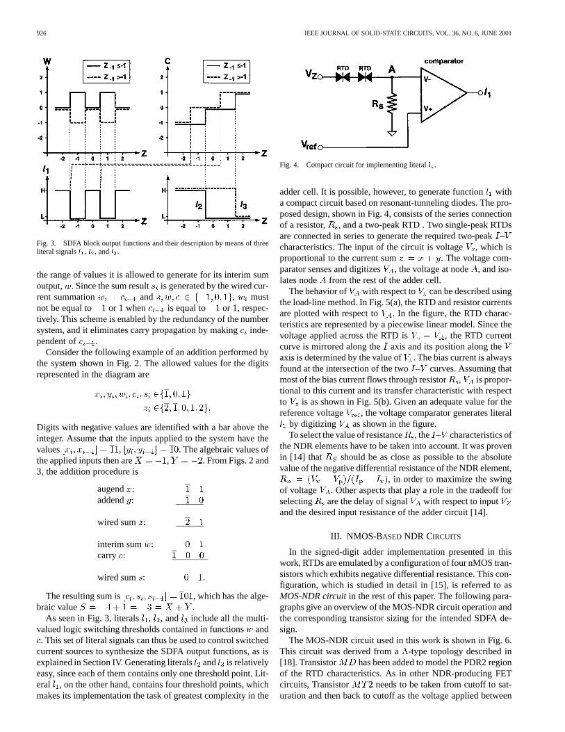
Fig. 4. Compact circuit for implementing literall .
adder cell. It is possible, however, to generate functionwitha compact circuit based on resonant-tunneling diodes. The pro-posed design, shown in Fig. 4, consists of the series connectionof a resistor, , and a two-peak RTD . Two single-peak RTDsare connected in series to generate the required two-peak–characteristics. The input of the circuit is voltage, which isproportional to the current sum . The voltage com-parator senses and digitizes, the voltage at node , and iso-lates node from the rest of the adder cell.
The behavior of with respect to can be described usingthe load-line method. In Fig. 5(a), the RTD and resistor currentsare plotted with respect to . In the figure, the RTD charac-teristics are represented by a piecewise linear model. Since thevoltage applied across the RTD is , the RTD currentcurve is mirrored along the axis and its position along theaxis is determined by the value of. The bias current is alwaysfound at the intersection of the two– curves. Assuming thatmost of the bias current flows through resistor, is propor-tional to this current and its transfer characteristic with respectto is as shown in Fig. 5(b). Given an adequate value for thereference voltage , the voltage comparator generates literal
by digitizing as shown in the figure.To select the value of resistance, the – characteristics of
the NDR elements have to be taken into account. It was provenin [14] that should be as close as possible to the absolutevalue of the negative differential resistance of the NDR element,
, in order to maximize the swingof voltage . Other aspects that play a role in the tradeoff forselecting are the delay of signal with respect to inputand the desired input resistance of the adder circuit [14].
III. NMOS-BASED NDR CIRCUITS
In the signed-digit adder implementation presented in thiswork, RTDs are emulated by a configuration of four nMOS tran-sistors which exhibits negative differential resistance. This con-figuration, which is studied in detail in [15], is referred to asMOS-NDR circuitin the rest of this paper. The following para-graphs give an overview of the MOS-NDR circuit operation andthe corresponding transistor sizing for the intended SDFA de-sign.
The MOS-NDR circuit used in this work is shown in Fig. 6.This circuit was derived from a -type topology described in[18]. Transistor has been added to model the PDR2 regionof the RTD characteristics. As in other NDR-producing FETcircuits, Transistor needs to be taken from cutoff to sat-uration and then back to cutoff as the voltage applied between

GONZLEZ et al.: CMOS IMPLEMENTATION OF A MULTIPLE-VALUED LOGIC SIGNED-DIGIT FULL ADDER 927
Fig. 5. (a) The load-line method is used to describe the behavior of the voltageat nodeA. (b) Generation of literall by comparison of voltageV to referencevoltageV .
Fig. 6. The four-transistor MOS-NDR circuit emulates the RTDI–Vcharacteristics. Two possible ways of applyingV are shown.
nodes and increases. To achieve this, the voltage at the gateof has to decrease as the applied voltage increases, whichis made possible by connecting the gate of to the outputof the inverter formed by and . It is to be noted thatthe bias voltage for the inverter can be applied at any one of thetwo positions shown in Fig. 6.
Fig. 7 shows the simulated variation in the current–voltagecharacteristics between terminalsand of the MOS-NDRcircuit as the sizes of Transistors and are changed.If the ratio of is increased, decreases faster asrises, and hence the NDR region occurs at a lower voltage re-ducing both and . This is shown in Fig. 7(a). When ismade wider, the drawn current increases, causingto increasewhile remains the same, as shown in Fig. 7(b).
Even though device and process engineers describe an RTDby means of its peak-to-valley current ratio (PVCR) and peakcurrent density (PCD), circuit designers are usually concernedwith the five parameters , , , , and when it comesto designing an RTD-based digital circuit. It is therefore impor-tant that the MOS-NDR circuit can be sized to generate an–curve which has the same, or approximately the same, five pa-rameter values.
To find the best transistor sizing in the MOS-NDR circuitsuch that a given RTD characteristic is emulated, the followingmethodology is used. First, hand calculations are performed toderive approximate transistor sizes for achieving the peak region
Fig. 7. Simulation results showing the effect of varyingW=L of (a)MT1 and(b)MT2 while holdingV constant.
specifications. Using SPICE simulation, it is then verified if theresulting circuit produces approximately an RTD-like charac-teristic with a significant NDR region. Next, starting from thehand-calculated sizes, a circuit optimization tool is used to findthe optimal values of the transistor sizes that would give thebest possible fit for the target current and voltage values. Thetool that has been used for this purpose is CUMIN [19], whichis a SPICE-based flexible direct-search optimization softwarein which any arbitrary cost-function can be defined very easily.The following cost function has been defined and used in sizingthe MOS-NDR circuit:
Cost
where variables with a caret represent the values correspondingto a particular circuit.
Using the method described above and the current–voltagecharacteristics required for the SDFA circuit, an optimal sizingfor the MOS-NDR circuit was obtained. The optimization wascarried out using the 0.6-m MOSIS CMOS process parame-ters, where the specified zero-bias threshold voltages for N and

928 IEEE JOURNAL OF SOLID-STATE CIRCUITS, VOL. 36, NO. 6, JUNE 2001
Fig. 8. (a) SimulatedI–V characteristics of the sized NDR circuit. (b)Two-peak current–voltage characteristics of two MOS-NDR circuits connectedin series with appliedV of 4 and 4.25 V.
P devices are, respectively, V and V.The resulting sizes are presented in Table II, and Fig. 8(a) showsthe simulated – characteristics of the optimized circuit with
V. Notice that the obtained current–voltage char-acteristics (solid line) and the intended characteristics (dottedline) are very similar. Since a two-peak– curve is required inthe SDFA cell, two instances of the MOS-NDR circuit are con-nected in series, as is done with actual RTDs when a multipeakcharacteristic is needed. The ability of the MOS-NDR circuitto produce multipeak characteristics was verified, as shown inFig. 8(b).
The fast switching speeds of the RTDs in conjunction withtheir bistable nature can be utilized to design several types oflogic styles [20]. Such logic styles could potentially lead tocompact high-performance digital circuits and systems. For in-stance, binary logic styles using RTD–CMOS combination havebeen explored and system application of such building blockshas been evaluated [21]. The MOS-NDR prototyping methodused in the research presented in this paper has recently beensuccessfully applied to the emulation of such binary QMOSlogic gates [15]. Other types of logic styles using RTDs couldsimilarly be redesigned using the method presented here. Inci-dentally, digital logic circuits are not the only beneficiaries of
TABLE IIMOS-NDR OPTIMIZATION RESULTS
Fig. 9. SDFA cell circuit schematic diagram.
the NDR characteristics of devices such as RTDs. It has beenshown that NDR circuits can be useful in low-loss inductor de-sign. Such techniques are common in CMOS RF circuit design(for example, [22]). The applicability of our current method tosuch cases is beyond the scope of this paper.
IV. CIRCUIT IMPLEMENTATION
If literals , , and , shown in Fig. 3, are available, it isrelatively easy to generate theand SDFA output functionsby means of switched current sources. This idea is used in thesigned-digit adder cell circuit shown in Fig. 9.
Three voltage comparators, one for each literal, are used inthe circuit. The generation of by means of two NDR circuits,a resistor, and a voltage comparator has been discussed in Sec-tion II. Literals and can be implemented by threshold de-tection circuits using voltage comparators. The threshold levelsof these circuits match the switching points of output function
when . The reference voltages for the comparatorsare primary inputs of the chip for greater prototype flexibility,but it will not be difficult to generate the threshold levels inter-nally once the technology is fully developed.
The voltage comparator used in this prototype consists of asimple source-coupled differential pair, a current-mirror pull-upconfiguration, and three static CMOS inverters in the outputstage. The purpose of the output inverters is to provide signalbuffering and to generate the complements of the literals as wellas their true values. Availability of the literal signals and theircomplements allows the use of a single type of transistors in thecircuitry which generates current output signalsand .

GONZLEZ et al.: CMOS IMPLEMENTATION OF A MULTIPLE-VALUED LOGIC SIGNED-DIGIT FULL ADDER 929
Fig. 10. SDFA cell layout for a 0.6-�m process. The expanded block corresponds to the MOS-NDR subcircuit. Dimensions are noted in micrometers.
Output currents and are generated by means of transis-tors through , seen in Fig. 9, as follows. Output function
requires only three MOS transistors. This part of the circuitis simple due to the similarity between functionand literal
. Transistor injects a current equivalent to one logic levelwhen is high. These states correspond to in thetransfer function shown in Fig. 3. States are han-dled by transistors and , which inject a current equiv-alent to two logic levels or no current at all, depending uponthe value of . In the portion of the circuit corresponding tooutput , transistors and produce the basic stairwayform of the carry function for . Transistors and
ensure that the correct output current levels for signalareproduced when . This is achieved by injecting a cur-rent equivalent to one logic level at the operating points whereoutput is affected by the value of , that is, at .In the circuit diagram of Fig. 9, is a binary signal whichindicates if . To our advantage, the behavior ofis identical to that of literal , as seen in Fig. 3. For this reason,output is taken directly from the second comparator ofthe SDFA circuit. In a parallel signed-digit adder, portsand of contiguous stages are connected together. Notice,however, that a carry propagation chain is not formed, since ateach stage is not a function of .
Layout for the circuit shown in Fig. 9 has been designed andfabricated using a standard 0.6-m CMOS process technology.The resulting layout is presented in Fig. 10, which also showsan expanded closeup view of the MOS-NDR subcircuit. Fig. 11shows a chip microphotograph of the fabricated circuit. TheSDFA layout occupies an area of 4789.125m . Of this area,only 531.36 m (11.1%) is used by the two MOS-NDR sub-circuits. The layout shown in Fig. 10 includes the resistorand two output load resistors implemented by MOS transistorsbiased as active load elements. The two output load resistors actas transducers which permit easy observation of output currents
and by means of simple voltage measurements.
Fig. 11. Chip microphotograph of fabricated signed-digit adder prototype.
V. RESULTS AND DISCUSSION
Functionality of the signed-digit adder prototype has beenverified through experimental measurements. Fig. 12 presentsoscilloscope traces which confirm correct operation of theSDFA cell. As seen in the figure, measurements were made forthe two possible values of the condition versus 1. Themeasured dc transfer characteristics are in good agreement withthe intended output functions, seen in Fig. 3. However, thereexists a noticeable difference in the logic levels of the measuredoutput signals and the desired functions. For example, whilethe difference between levels1 and 0 of voltage is around300 mV, the swing between levels 0 and1 is 450 mV. Thispeculiarity arises because the output signal is measured inthe prototype by converting the output currents into voltagesby means of on-chip active loads. It is necessary to point outthat the axis of the signal traces shown in Fig. 12 describesinput voltage , but in oscilloscope traces theaxis usuallycorresponds to time. To carry out this measurement, the inputsignal had to be ramped with an extremely low slow rate. Itwas possible, in this way, to confidently arrange the traces as

930 IEEE JOURNAL OF SOLID-STATE CIRCUITS, VOL. 36, NO. 6, JUNE 2001
(a) (b)
Fig. 12. Measured results at low speed showing the transfer characteristics of the SDFA cell. (a)InZ = L. (b) InZ = H .
dc transfer curves. This measurement is useful in determiningthe voltage levels, 1.3, 2.0, 2.7, 3.4, and 4.1 V, of input signal
which correspond to logic levels “2” through “ 2,”respectively.
A good estimate of speed performance for the adder circuitcan be obtained from computer-aided circuit simulation.In order to make this estimate as accurate as possible, thesimulation model includes parasitic elements introduced bythe interconnecting wires. The estimated worst-case delay forthe circuit is 17 ns, and it is for the transition of input fromlogic level “ 1” to level “ 2”, that is, from 3.4 to 4.1 V. Notethat this delay corresponds to the intrinsic circuit performance,since in the experiment the circuit drives no additional outputload besides the layout parasitic capacitances and the capac-itances of the circuit transistors. Fig. 13 shows oscilloscopetraces corresponding to an experiment which was carried out tomeasure the propagation delay of the SDFA prototype circuit.The experimentally measured delay—1.4s—is much higherthan the delay estimated by simulation. This large delay iscaused by the fact that the SDFA circuits produce weak multi-valued voltage signals since the output currents are convertedto voltages by means of active loads working as transducers.These weak signals, in turn, have to drive the large chip outputpads and the load presented by the inputs of the measurementinstrument (oscilloscope). Moreover, the experimental setupwas not designed for precise measurements of high-speedparameters and, hence, additional parasitics and delays thatcannot be included in the simulation model may be present.
Table III presents a comparison of three implementations ofidentical SDFA circuits. The first column includes the layout,circuit area, and worst-case delay of a hybrid RTD–CMOSprototype, the second column contains similar informationfor the MOS-NDR implementation, and the third columnpresents a QMOS SDFA that assumes viable RTD-MOScointegration. The worst-case delay in all columns was ob-
Fig. 13. Measurement of worst case gate delay, including delay of the chippads.
tained by computer-aided simulation of circuits extractedfrom the layout geometries, including parasitic capacitances.In the table, the circuit layout images are drawn to scale andall implementations are based on the same 0.6-m processtechnology. As was explained earlier in the paper, the hybridRTD–CMOS technique consists of fabricating the RTDs on aIII–V substrate and then grafting the RTDs onto the Siliconsubstrate containing the prefabricated CMOS portion of thecircuit. As shown in Table III, the circuit area of the hybridRTD–CMOS prototype is more than 15 times that of theMOS-NDR implementation due to the enormous size of theRTD landing area and its bonding pads as compared to the areaof the CMOS circuitry. Also shown in Table III is the fact thatthe worst-case propagation delay of the MOS-NDR SDFA iscomparable to that of the hybrid RTD–CMOS prototype whileit uses a significantly smaller area.
The MOS-NDR approach is a prototyping technique thatallows efficient verification of circuit concepts based on NDR

GONZLEZ et al.: CMOS IMPLEMENTATION OF A MULTIPLE-VALUED LOGIC SIGNED-DIGIT FULL ADDER 931
TABLE IIISDFA PROTOTYPECOMPARISON
devices. MOS-NDR is not intended as the final realizationof a given design. Instead, projected figures for the intendedRTD-MOS circuit more accurately reflect the potential ofNDR circuits assuming a viable process technology. It shouldbe noted that as compared to the result presented in Table I,the delay value of the QMOS SDFA reported in Table IIIis larger since the circuits compared in Table III utilizevoltage comparators for literal generation instead of the fasterthreshold-modified inverters used in [14]. Comparators areused in this design to allow for variations in the post-fabrication– characteristics of the MOS-NDR circuits. These variations
may occur because of nonavailability, at the time of design, ofbinned SPICE device models that can very accurately modeltransistors with widely varying -ratios such as those usedin the MOS-NDR circuits.
VI. CONCLUSION
The implementation of a signed-digit full adder circuit basedon NDR devices has been presented. The SDFA circuit proto-type takes advantage of MOS-NDR, a new prototyping tech-nique proposed in [15]. The MOS-NDR technique enabled thedesign and fabrication of a fully integrated version of the addercircuit using a standard 0.6-m CMOS process technology. Thenew SDFA implementation provides a 15:1 reduction in circuitarea, as compared to the area of a hybrid RTD–CMOS versionof the same circuit. At the same time, the worst-case propaga-tion delay of the MOS-NDR prototype is similar to that of thehybrid RTD–CMOS SDFA implementation. A disadvantage ofthe MOS-NDR implementation technique is that the RTD-emu-lating circuit requires a bias voltage. In our design, since twoRTDs are connected in series, two separate bias voltages arenecessary.
REFERENCES
[1] A. Avizienis, “Signed-digit number representations for fast parallelarithmetic,”IRE Trans. Electron. Comput., pp. 389–400, Sept. 1961.
[2] S. Kawahito, M. Kameyama, T. Higuchi, and H. Yamada, “A32�32-bitmultiplier using multiple-valued MOS current-mode circuits,”IEEE J.Solid-State Circuits, vol. 23, pp. 124–132, Feb. 1988.
[3] H. Makino, Y. Nakase, H. Susuki, H. Morinaka, H. Shinohara, and K.Mashiko, “An 8.8-ns54� 54-bit multiplier with high speed redundantbinary architecture,”IEEE J. Solid-State Circuits, vol. 31, pp. 773–783,June 1996.
[4] M. Kameyama, T. Sekibe, and T. Higuchi, “Highly parallel residue arith-metic chip based on multiple-valued bidirectional current-mode logic,”IEEE J. Solid-State Circuits, vol. 24, pp. 1404–1411, Oct. 1989.
[5] M. Kameyama, M. Nomura, and T. Higuchi, “Modular design of mul-tiple-valued arithmetic VLSI system using signed-digit number system,”in Proc. Int. Symp. Multiple-Valued Logic, 1990, pp. 355–362.
[6] F. Capasso, S. Sen, F. Beltram, L. M. Lunardi, A. S. Vengurlekar, P. R.Smith, N. J. Shah, R. J. Malik, and A. Y. Cho, “Quantum functional de-vices: Resonant-tunneling transistors, circuits with reduced complexity,and multiple-valued logic,”IEEE Trans. Electron Devices, vol. 36, pp.2065–2082, Oct. 1989.
[7] R. Tsu and L. Esaki, “Tunneling in a finite superlattice,”Appl. Phys.Lett., vol. 22, pp. 562–564, 1973.
[8] T. Hanyu, M. Kameyama, and T. Higuchi, “Prospects of multiple-valuedVLSI processors,”IEICE Trans. Electron., vol. E76-C, pp. 383–391,Mar. 1993.
[9] K. C. Smith, “The prospects for multivalued logic: A technology andapplication view,”IEEE Trans. Comput., vol. C-30, pp. 619–634, Sept.1981.
[10] S. L. Rommel, T. E. Dillon, P. R. Berger, R. Lake, P. E. Thompson,K. D. Hobart, A. C. Seabaugh, and D. S. Simons, “Si-based interbandtunneling devices for high-speed logic and low power memory ap-plications,” in Proc. IEEE Int. Electron Devices Meeting, 1998, pp.1035–1037.
[11] A. Seabaugh, R. Lake, B. Brar, R. Wallace, and G. Wilk, “Be-yond-the-roadmap technology: Silicon heterojunctions, optoelectronics,and quantum devices,” inProc. 1997 MRS Symp., vol. 486, 1997, pp.67–77.
[12] J. Randall, G. Frazier, A. Seabaugh, and T. Broekaert, “Potential nano-electronic integrated circuit technologies,”Microelectron. Eng., vol. 32,pp. 15–30, Sept. 1996.
[13] A. F. González, M. Bhattacharya, S. Kulkarni, and P. Mazumder, “Stan-dard CMOS implementation of a multiple-valued logic signed-digitadder based on negative differential-resistance devices,” inProc. Int.Symp. Multiple-Valued Logic, 2000, pp. 323–328.
[14] A. F. González and P. Mazumder, “Multiple-valued signed-digit adderusing negative differential-resistance devices,”IEEE Trans. Comput.,vol. 47, pp. 947–959, Sept. 1998.
[15] M. Bhattacharya, S. Kulkarni, A. Gonzalez, and P. Mazumder, “A Pro-totyping technique for large-scale RTD–CMOS circuits,” inProc. IEEEInt. Symp. Circuits and Systems, May 2000, pp. I-635–I-638.
[16] J. I. Bergman, J. Chang, Y. Joo, B. Matinpour, J. Laskar, N. M. Jok-erst, M. A. Brooke, B. Brar, and E. Beam, “RTD/CMOS nanoelectroniccircuits: Thin-film InP-based resonant tunneling diodes integrated withCMOS circuits,”IEEE Electron Device Lett., vol. 20, pp. 119–122, Mar.1999.

932 IEEE JOURNAL OF SOLID-STATE CIRCUITS, VOL. 36, NO. 6, JUNE 2001
[17] N. Evers, O. Vendier, C. Chun, M. R. Murti, J. Laskar, N. M. Jokerst, T.S. Moise, and Y.-C. Kao, “Thin film pseudomorphic AlAs/InGaAs/InAsresonant tunneling diodes integrated onto Si substrates,”IEEE ElectronDevice Lett., vol. 17, pp. 443–445, Sept. 1996.
[18] C.-Y. Wu and C.-Y. Wu, “The new general realization theory of FET-likeintegrated voltage-controlled negative differential resistance devices,”IEEE Trans. Circuits Syst., vol. 28, pp. 382–390, May 1981.
[19] M. Bhattacharya. (1998) CUMIN: A circuit optimiza-tion framework using SPICE. [Online]. Available:http://www.eecs.umich.edu/~mayukh/cumin
[20] P. Mazumder, S. Kulkarni, M. Bhattacharya, J. P. Sun, and G. I. Haddad,“Digital circuit applications of resonant tunneling devices,”Proc. IEEE,vol. 86, pp. 664–686, Apr. 1998.
[21] S. Kulkarni and P. Mazumder, “Circuit applications of quantum MOSlogic,” in Proc. Eur. Conf. Circuit Theory and Design, 1999, pp.667–670.
[22] E. Abou-Allam, E. I. El-Masry, and T. Manku, “CMOS front-end RFamplifier with on-chip tuning,” inProc. IEEE Int. Symp. Circuits andSystems, vol. 1, 1996, pp. 148–151.
Alejandro F. González(S’96) received the B.E. de-gree in electrical engineering (Licenciado en Inge-niería Electrónica) from the Instituto Tecnológico yde Estudios Superiores de Occidente, Guadalajara,Mexico, in 1993 and the M.S.E. degree in electricalengineering from the University of Michigan, AnnArbor, in 1995. He is currently working toward thePh.D. degree in electrical engineering at the Univer-sity of Michigan. His research interests include ultra-fast digital circuit design, multiple-valued logic, andVLSI design automation.
Mayukh Bhattacharya received the B.Tech.degree in electronics and electrical communicationengineering from the Indian Institute of Technology,Kharagpur, in 1992, the M.S. degree in electricalengineering from the Virginia Polytechnic Instituteand State University, Blacksburg, in 1994, and thePh.D. degree in computer science and engineeringfrom the University of Michigan, Ann Arbor, in1999.
He is currently a Research Fellow at the Univer-sity of Michigan. His research interests include very-
large-scale-integration (VLSI) circuit simulation, CAD for VLSI, deep-submi-cron defect and fault modeling, and emerging technologies.
Shriram Kulkarni received the B.E. degree inelectronics and communication engineering from theKarnataka Regional Engineering College, India, andthe M.S. and Ph.D. degrees in electrical engineeringfrom the University of Michigan, Ann Arbor.
Since 1999, he has been a Research Fellow withthe Department of Electrical Engineering and Com-puter Science, University of Michigan. His researchinterests include design and optimization of ultrafastcircuits, and VLSI physical design automation.
Pinaki Mazumder (S’84-M’87-SM’95-F’99) re-ceived the B.S.E.E. degree from the Indian Instituteof Science in 1976, the M.Sc. degree in computerscience from the University of Alberta, Alberta,Canada, in 1985, and the Ph.D. degree in electricaland computer engineering from the University ofIllinois, Urbana-Champaign, in 1987.
For two years, he was a Research Assistant with theCoordinated Science Laboratory, University of Illi-nois at Urbana-Champaign. For more than six years,he was with Bharat Electronics Ltd. (a collaborator of
RCA), Bangalore, India, where he developed analog and digital integrated cir-cuits for consumer electronics products. During the summers of 1985 and 1986,he was a Member of Technical Staff in the Naperville, IL, branch of AT&T BellLaboratories. He spent his sabbatical year as Visiting Faculty at Stanford Uni-versity, Stanford, CA, University of California, Berkeley, and at Nippon Tele-graph and Telephone (NTT), Japan. He is presently with the Department of Elec-trical Engineering and Computer Science, University of Michigan, Ann Arbor.His research interests include VLSI testing, physical design automation, and ul-trafast digital circuit design. He has written over 100 papers on archival journaland international conference proceedings on these topics. He has co-authoredtwo books entitledTesting and Testable Design of Random Access Memories(Norwell, MA: Kluwer, 1996) andGenetic Algorithms for VLSI Layout and TestAutomation(Englewood Cliffs, NJ: Prentice Hall, 1998).
Dr. Mazumder was a recipient of Digital’s Incentives for Excellence Award,National Science Foundation Research Initiation Award, and Bell NorthernResearch Laboratory Faculty Award. He is an Associate Editor of IEEETRANSACTIONS ON VERY LARGE SCALE INTEGRATION (VLSI) SYSTEMS. Hewas a Guest Editor of theIEEE Design and Test Magazinespecial issue onmultimegabit memory testing, March 1993, a Guest Editor of theJournalof Electronic Testing: Theory and Applicationsspecial issue on advancedtechniques for memory testing, April 1994, and a Guest Editor of the IEEETRANSACTIONS ON VLSI SYSTEMS special issue on the impact of emergingtechnologies in VLSI systems, March 1998. He is a member of Sigma Xi, PhiKappa Phi, and the Association for Computing Machinery Special InterestGroup on Design Automation.

Title: Redundant Arithmetic, Algorithms andImplementations
Authors: Alejandro F. Gonzalez and Pinaki Mazumder
Affiliation: The University of Michigan,Department of Electrical Engineering and Computer Science
Abstract: Performance in many very-large-scale integrated (VLSI) systems such as digitalsignal processing (DSP) chips, is predominantly determined by the speed of arith-metic modules like adders and multipliers. Even though redundant arithmetic algo-rithms produce significant improvements in performance through the elimination ofcarry propagation, efficient circuit implementations of these algorithms have beentraditionally difficult to obtain. This work presents a survey of circuit implemen-tations of redundant arithmetic algorithms. The described implementations are di-vided in three main groups: 1) conventional binary logic circuits, which encode themultivalued digits of redundant arithmetic into two or more binary digital signals;2) current-mode multiple-valued logic circuits, which directly represent multival-ued redundant digits using non-binary digital current signals; and 3) heterostructureand quantum electronic circuits, intended for very compact designs capable of op-erating at extremely high speeds. For each of the circuits, the operating principle isdescribed and the main advantages and disadvantages of the approach are discussedand compared.
Keywords: Redundant number systems; redundant binary logic; current-mode logic; multiple-valued logic; quantum electronic circuits
SubmissionRecord:
This is a survey paper which contains information on work published by several au-thors. This paper has not been previously published, and it is not being consideredfor publication by any other journal.
Contact Author: Prof. Pinaki Mazumder
Address: The University of MichiganEECS Building, Room 22151301 Beal AvenueAnn Arbor, MI 48109-2122
Phone: (734) 763-2107
Fax: (734) 763-1503
E-Mail: [email protected]

A. F. Gonzalez and P. Mazumder 2
Alejandro F. Gonzalez received the B.E. degree in electrical engineering (Licenciado en Ingenierıa Electro-nica) from the Instituto Tecnologico y de Estudios Superiores de Occidente, Guadalajara, Mexico, in 1993and the M.S.E. degree in electrical engineering from the University of Michigan, Ann Arbor, in 1995. Heis currently pursuing the Ph.D. degree in electrical engineering at the University of Michigan. His researchinterests include ultrafast digital circuit design, multiple-valued logic, and VLSI design automation.
Pinaki Mazumder received the B.S.E.E. degree from the Indian Institute of Science in 1976, the M.Sc. de-gree in computer science from the University of Alberta, Canada, in 1985, and the Ph.D. degree in electricaland computer engineering from the University of Illinois at Urbana-Champaign in 1987.
For two years, he was a Research Assistant with the Coordinated Science Laboratory, University ofIllinois at Urbana-Champaign. For more than six years, he was with Bharat Electronics Ltd. (a collaboratorof RCA), India, where he developed analog and digital integrated circuits for consumer electronics products.During the summers of 1985 and 1986, he was a Member of Technical Staff in the Naperville branch ofAT&T Bell Laboratories. He spent his sabbatical year as a visiting faculty at Stanford University, Universityof California, Berkeley, and also at Nippon Telegraph and Telephone (NTT), Japan. He is presently with theDepartment of Electrical Engineering and Computer Science of the University of Michigan, Ann Arbor. Hisresearch interests include VLSI testing, physical design automation, and ultrafast digital circuit design. Hehas written over 100 papers on archival journal and international conference proceedings on these topics.He has coauthored two books entitled, Testing and Testable Design of Random Access Memories (Kluwer1996) and Genetic Algorithms for VLSI Layout and Test Automation (Prentice Hall, 1998).
Dr. Mazumder was a recipient of Digital’s Incentives for Excellence Award, National Science Founda-tion Research Initiation Award, and Bell Northern Research Laboratory Faculty Award. He is an AssociateEditor of IEEE Transactions on Very Large Scale Integration (VLSI) Systems. He was a Guest Editor in IEEEDesign and Test Magazine’s special issue on multimegabit memory testing, March 1993, a Guest Editor inJournal of Electronic Testing: Theory and Applications’ special issue on advanced techniques for memorytesting, April 1994, and a Guest Editor of IEEE Transactions on VLSI Systems’ special issue on the impactof emerging technologies in VLSI systems, March 1998. He is a member of Sigma Xi, Phi Kappa Phi, andthe Association for Computing Machinery Special Interest Group on Design Automation.

Redundant Arithmetic, Algorithms andImplementations1
Alejandro F. Gonzalez and Pinaki Mazumder
The University of MichiganElectrical Engineering and Computer Science Department
1301 Beal Ave., Room 2215Ann Arbor, MI 48109-2122
Phone: (734) 763-2107E-Mail: falgonz,[email protected]
Abstract
Performance in many very-large-scale integrated (VLSI) systems such as digital signal pro-cessing (DSP) chips, is predominantly determined by the speed of arithmetic modules like addersand multipliers. Even though redundant arithmetic algorithms produce significant improvementsin performance through the elimination of carry propagation, efficient circuit implementations ofthese algorithms have been traditionally difficult to obtain. This work presents a survey of circuitimplementations of redundant arithmetic algorithms. The described implementations are dividedin three main groups: 1) conventional binary logic circuits, which encode the multivalued digits ofredundant arithmetic into two or more binary digital signals; 2) current-mode multiple-valued logiccircuits, which directly represent multivalued redundant digits using non-binary digital current sig-nals; and 3) heterostructure and quantum electronic circuits, intended for very compact designscapable of operating at extremely high speeds. For each of the circuits, the operating principle isdescribed and the main advantages and disadvantages of the approach are discussed and compared.
Keywords: Redundant number systems; redundant binary logic; current-mode logic; multiple-valuedlogic; quantum electronic circuits
1This work was supported by the U.S. Army Research Office under the URI program, by the Defense Advanced ResearchProjects Agency, and by the National Science Foundation

A. F. Gonzalez and P. Mazumder 1
1 Introduction
Increasing the speed of arithmetic logic circuits has been, and still is, of extreme importance in the field
of computing and signal processing circuits. On one hand, throughputs of the order of few gigaoper-
ations per second are now conventional in large scientific vector processors and supercomputers [1].
This kind of performance is usually achieved by means of fast, densely integrated circuit technologies
and highly parallel organizations. On the other hand, advanced signal processors with clock rates of the
order of gigahertz are required for future system applications such as digital microwave receivers [1].
Speed in these processors is usually limited by the latency of their arithmetic units, especially that of
multipliers.
Carry signals propagating through long chains of logic, as is the case in conventional ripple-carry
adders, significantly hurt performance in arithmetic systems. In conventional adders, the worst-case la-
tency is proportional to the number of digits involved in the operation, that is, the size of the operands.
Moreover, multiplier circuits cascade a number of adders to sum the partial products. The importance
of carry propagation effects is evident, considering that operand sizes tend to increase with the con-
stant strive for greater processor power and precision. A standard for floating point arithmetic [2], for
example, specifies 52-bit mantissas for the double-precision floating-point operands. Having addition
latency proportional to 52 times the delay of an adder cell is obviously unacceptable, considering that
the length of logic paths between latches is highly constrained in modern pipelined high-performance
microprocessors.
Redundant number systems reduce or eliminate carry propagation chains in digital arithmetic cir-
cuits. In these number systems, redundancy is owed to the fact that, contrary to the case of conventional
systems, redundant numbers can have more than one representation. For instance, in a radix-4 system
with the digit set f�2��1�0�1�2g, numbers 0020, 0100, 1020, and 1100 all have arithmetic value 8.
Redundancy allows addition algorithms in which carry propagation is completely eliminated. In these
algorithms, a proper intermediate representation of the operand digit summation, x i �yi, is selected so
that the final addition result can be generated using half-adders that do not require nor generate carry
signals. More details on redundant arithmetic systems are given in Section 2.
Even though redundant addition techniques offer great improvements in computing performance,
efficient circuit implementations of these algorithms have been traditionally difficult to achieve. A

A. F. Gonzalez and P. Mazumder 2
simple way to understand these difficulties is by noting the fact that digits in redundant systems are
often not binary. This forces a departure from traditional binary logic circuits and conventional circuit
techniques and technologies. In this work, we survey digital circuit implementations of redundant
arithmetic algorithms. Conventional binary logic circuit techniques, described in Section 3,have been
applied in redundant arithmetic systems by encoding redundant multivalued digits into two or more
binary signals. It is interesting to study the evolution of circuit implementations of redundant arithmetic
systems and appreciate the different circuit techniques that have been inspired. Such circuit techniques
often explore non-traditional areas of digital circuit design. Section 4 presents multiple-valued logic
and current-mode circuits. These circuits are intend as a better match of the need for operation with non-
binary digits. Heterostructure and quantum devices are used in alternative circuit techniques, described
in Section 5, intended for very compact designs capable of operating at extremely high speeds.
2 Redundant Number Systems
This section presents the basic concepts of redundant arithmetic. Signed-digit arithmetic [3], a special
case of redundant arithmetic, is described in more detail and is used to introduce the properties that
characterize redundant arithmetic systems. Such properties include, among others, the number format,
the addition algorithm, the valid digit set, and the proper radix values. Other redundant number systems
are addressed using Parhami’s unifying generalized signed-digit number representation [4].
2.1 Signed-digit number representations
Signed-digit systems were conceived with the purpose of implementing totally-parallel addition [3],
where carry propagation is eliminated. Carry propagation is eliminated by making each digit of the
resulting sum a function of only two input digits. This is made possible by the redundancy of the
number representation since a proper intermediate representation of the operand digit summation, x i �
yi, is selected so that the final addition result can be generated using half-adders that do not require nor
generate carry signals. The totally-parallel addition algorithm can also be used to perform subtraction
operations. The followingparagraphs present the most important characteristics of signed-digit systems
and the basic principles of the corresponding addition algorithm.

A. F. Gonzalez and P. Mazumder 3
x
Step 1
Step 2
x y
x
c w c w
y y
x y
w w c w
s s
c
i+1 i
i i-1 i-1ii+1
i i i-1 i-1
w c
s
w c
s
Figure 1: Totally-parallel addition approach in signed-digit number representation [3].
2.1.1 Properties of signed-digit number systems
The algebraic value of a signed-digit number is given by
Z �m
∑i��n
zir�i
where r is a positive integer called the radix. In a redundant representation with radix r, each digit can
assume more than r values, whereas in conventional number representations digits can assume exactly
r values. The values of the radix and the number digits, z i, should satisfy the condition of a unique
representation for the algebraic value Z � 0. It is then easy to prove that the algebraic value Z is zero if,
and only if, all digits of its signed-digit representation have the value z i � 0. It is also evident that the
sign of the algebraic value Z is determined by the sign of the most significant non-zero digit. Similarly,
the signed-digit representation of �Z, the additive inverse of Z, is obtained by changing the sign of
every non-zero zi digit of Z.
Fig. 1 depicts the totally-parallel addition approach in the signed-digit arithmetic system. The
addition of two digits x i and yi is totally-parallel if two conditions are satisfied. First, the sum digit s i is
function only of the operand digits, x i and yi, and the carry digit ci�1 from the adjacent digit position.
Second, the carry digit to the next position c i is function only of the operand digits, x i and yi. Totally-
parallel subtraction xi �yi is realized as the totally-parallel addition of x i and the additive inverse of yi,
that is, xi�yi � xi ���yi�.
Totally-parallel addition of two digits is performed in two steps, as depicted in Fig. 1. In the first
step, a transfer digit output ci and an interim sum output wi are generated such that
xi �yi � rci �wi� (1)

A. F. Gonzalez and P. Mazumder 4
In the second step, the final sum digit s i is obtained as
si � wi �ci�1� (2)
The required and allowed digit values for each of the variables involved in the two-step addition
process can be derived from the definition of totally-parallel addition and from the addition algorithm
described by (1) and (2). The most important results of such derivation are as follows (for a complete
analysis see [3]):
1. The smallest sufficient set of values for the carry digit is c i � f�1�0�1g.
2. The upper bound for the magnitude of the interim sum is jw ij � r�2.
3. The lower bound for the radix value is r � 2.
4. For an odd radix, ro � 3, the required (minimum) set of values for operand digits x i and yi consists
of the sequence of ro�2 integers
��
12�ro�1� � � � � ��1�0�1� � � � �
12�ro�1�
��
5. For an even radix, re � 4, the minimum set of values for operand digits xi and yi consists of the
sequence of re�3 integers
��
�12
re�1
�� � � � ��1�0�1� � � � �
12
re�1
��
Minimum sets are the only allowed for radix-3 and radix-4 systems. For r � 4, however, there is
more than one valid set of digit values. The sequence of integers
f�a���a�1�� � � � ��1�0�1� � � � �a�1�ag
meets the requirements for signed-digit number representations, where
12�ro�1�� a � ro�1 or
12
re�1 � a � re�1�
ro is an odd integer ro � 3, and re is an even integer re � 4. All signed-digit number representations can
be described in terms of the allowed radix values and the allowed z i digit values. The redundancy of a
signed-digit system is said to be minimal when a � 1�2�r o� 1� or a � 1�2re� 1, and the redundancy
is maximal when a � ro�1 or a � re�1.

A. F. Gonzalez and P. Mazumder 5
2.1.2 Signed-digit addition and subtraction
Two signed-digit numbers are added by means of the totally-parallel additionalgorithm described by (1)
and (2). The rules for obtaining wi, ci, and si can be determined given the set of allowed values of wi,
wmin and wmax, as follows. From (1),
wi � �xi �yi�� rci
where
ci �
�����������
0 if wmin � xi �yi � wmax
1 if xi�yi � wmax
�1 if xi�yi � wmin
and
si � wi �ci�1�
Example 2.1 — Signed-Digit Addition(Radix 10).
The allowed values for the digits are:
wi : 5�4�3�2�1�0�1�2�3�4�5;
ci : 1�0�1;
si�xi�yi : 6�5�4�3�2�1�0�1�2�3�4�5�6�
Digits with negative values are identified with a bar above the integer. The addition operands are
x � 4�25143 (algebraic value X � 3�75137), and y � 2�33021 (algebraic value Y � �2�32979). The
addition procedure is as follows:
augend x: 4 . 2 5 1 4 3
addend y: 2 . 3 3 0 2 1
Step 1): 0�2 0�5 10�2 0�1 10�4 0�2
Step 2): 0 1 0 1 0
Sum s: 2 . 6 2 2 4 2
The resulting sum is s� 2�62242, which has an algebraic value S� 1�42158� 3�75137�2�32979�

A. F. Gonzalez and P. Mazumder 6
2.2 Other redundant number systems
Stored-carry, stored-borrow, and the binary signed-digit (BSD) number systems are examples of other
useful redundant arithmetic systems. In [4], Parhami proposed a generalized signed-digit number rep-
resentation (GSD) where Avizienis’ signed-digit system is named the ordinary signed-digit number
system (OSD). In the generalized number system, the OSD and BSD systems are unified and other use-
ful redundant number representations such as stored-carry and stored-borrow are included as special
cases.
The generalized signed-digit number system is a positional system (a weight is associated with each
digit position) with the digit set f�α��α� 1� � � � �β� 1�βg, where α � 0, β � 0, α�β� 1 � r, and
r is the radix of the number representation. The excluded case α�β� 1 � r results in non-redundant
number representation systems which cover the conventional radix-r system with α � 0 β � r�1 as a
special case. GSD number systems cover the following special cases.
1. Binary stored-carry (BSC): r � 2, α � 0, β � 2
2. Radix-r stored-carry (SC): α � 0, β � r
3. Binary stored-borrow (BSB or BSD): r � 2, α� β � 1
4. Radix-r stored-borrow (SB): α � 1, β � r�1
5. Binary stored-carry-or-borrow (BSCB): r � 2, α � 1, β � 2
6. Radix-r stored-carry-or-borrow (SCB): α � 1, β � r
7. Minimally redundant symmetric signed-digit: 2α � 2β � r � 4
8. Ordinary signed-digit (OSD): r � 3, 12 r � α � β � r
Minimally redundant: α � β � b 12 rc�1
Maximally redundant: α � β � r�1
Radix-r stored-carry number representation systems use the digit set f0�1�2� � � � �rg. The special
case r � 2 leads to the binary stored-carry (BSC) number system. The main use of BSC numbers is in
multioperand addition (multiplication). A BSC number can be added to a conventional binary number,
producing a BSC result, using a set of full adders without carry propagation. The stored-carry number

A. F. Gonzalez and P. Mazumder 7
Table 1: Radix-2 Redundant Binary Encodings
Encoding Bit ValuesSign-mag Sign 0 0 1 1
Mag. 0 1 1 0Digit value 0 1 -1 X
Borrow-save Borrow 0 1 0 1Sum 0 1 1 0Digit value 0 0 1 -1
Carry-save Carry 0 0 1 1Sum 0 1 0 1Digit value 0 1 1 2
systems have been adopted in many implementations [5–8]. Radix-r stored-borrow number systems use
the digit set f1�0�1� � � � �r�1g. The special case r � 2 leads to the binary stored-borrow (BSB) number
system, also known as binary signed-digit (BSD) number system. BSD numbers have been used for
representing intermediate temporary values in high-speed multiplication and division algorithms such
as Booth’s recoding algorithm for multiplication [9]. Two BSD numbers can be added by a limited
carry circuit. Implementations using the BSD number system are described in [10–13].
3 The Redundant Binary Approach
In redundant binary logic, each redundant digit is encoded by two or more bits and computation is
performed by means of conventional binary logic families such as static or dynamic CMOS. A radix-2
redundant digit, for example, can be encoded by two binary digits as seen Table 1. The digit set
f1�0�1g has two well known encodings, namely, sign-mag and borrow-save [14]. In sign-mag the two
bits represent a magnitude and a sign, respectively, whereas in borrow-save one bit is positive (sum)
and the other is negative (borrow). This section describes implementations of redundant arithmetic
algorithms by means of conventional binary logic circuits.
The main use of redundant binary logic is in multipliers. In high-performance (parallel) multipliers,
most of the circuit area is dedicated to adder blocks which sum together partial products to generate the
final multiplication result. Consequently, the performance of this type of systems depends heavily on
the speed of the adder circuits. Multipliers are very suitable for redundant addition techniques because

A. F. Gonzalez and P. Mazumder 8
several stages of addition can be performed without conversion to the standard binary representation.
Most high-performance multipliers use a tree structure to increase parallelism in the addition of partial
products [15].
3.1 Early tree multipliers
In 1964, Wallace [15] proposed a fully combinational multiplier in which partial products are added
by a tree of pseudoadders. A pseudoadder sums together three binary numbers and produces two
output numbers whose sum equals that of the three inputs. The pseudoadder operates without carry
propagation and it can be implemented using full adders, with the third input number being fed to the
carry inputs of the full adders and the second output number being formed by the set of carry outputs
of the adder cells. By arranging a group of pseudoadders in a tree structure, several additions are
performed in parallel. This improves the speed of multiplication and makes the delay proportional to
the logarithm of the number of partial products. Fig. 2 depicts a 20-input Wallace tree made of 18
pseudoadders. The pseudoadder is also named a 3:2 compressor because it has three inputs and two
outputs. A lot of work has been done on the implementation of compressor-based multipliers, and the
4:2 compressor approach is one of the most popular at the present time [16–19].
The Wallace tree approach and other carry-save implementations [6] use redundant binary repre-
sentation. In these schemes, addition results are expressed as the sum of two numbers. A quantity
can therefore be represented in several different ways, thus making the system redundant. If the pair of
output numbers is considered as the addition result, it is easy to verify that the pseudoadder implements
totally-parallel addition by noting that each digit of the result is function only of the input digits of the
corresponding compressor.
To obtain the normal binary representation of the result, it is necessary to use a conventional adder
to sum the pair of resulting numbers. This step involves carry propagation, which implies a penalty
on performance. In multipliers this problem is compensated by accumulating the speed-up of several
compression steps before a single conventional addition takes place at the end of the process. The
process in which the two resulting numbers are added together can be regarded as a conversion from
redundant representation to normal binary representation [11].
In [6], a carry-save multiplication algorithm similar to the Wallace tree approach is described. The
basic difference between these schemes is that the carry-save adder produces the carry-save sum of two

A. F. Gonzalez and P. Mazumder 9
C SC SC S
C S C S C S C S
C S C S C S C S C S C S
C S
C SC S
C S
C S
Carry Propagating Adder
Final Sum
Level 1
Level 2
Level 3
Level 4
Level 5
Level 6
Level 7
120 16 14 13 12 11 10 8 7 6 5 4 3 2915171819 Partial products
Figure 2: Wallace tree for a 20-input adder.
carry-save inputs, while the Wallace tree pseudoadder produces the addition of three binary numbers
represented by the sum of two binary numbers. In a unifying way of describing the algorithms one
could say that Wallace uses 3:2 compressors and Vuillemin uses 4:2 compressors as the basic addition
elements.
Another type of redundant adder tree implementation is based on borrow-save or sing-mag rep-
resentations [11]. The main distinguishing characteristic of this approach is that digits can assume
negative values. While the digit set in the carry-save scheme is f0�1�2g, the set of digit values in the
borrow-save and sign-mag approaches is f1�0�1g. This digit set is characteristic of a radix-2 signed-
digit number system, which was named a modified signed-digit number system in [3]. Again, the
functional characteristics of this type of algorithms are not very different from those of the carry-save
methods. The signed-digit redundant binary adder can also be regarded as a 4:2 compressor.
Compressor-based multioperand addition schemes are very similar to each other. The main differ-
ence is in their theoretical basis and the way this drew the path to the corresponding addition algorithm
itself. The rest of this section presents practical VLSI implementations of redundant binary arithmetic
schemes. The designs described involve parallel multipliers that implement redundant arithmetic by
means of conventional binary logic. There are two main classes of multiplier implementations, taking

A. F. Gonzalez and P. Mazumder 10
the theoretical treatment of the arithmetic as the classification criterion, namely, carry-save multipliers
and redundant binary multipliers.
3.2 Carry-save multipliers
Most of the implementations under this category are based on Wallace’s approach [15]. Here, we
describe four of the most representative multiplier designs that have been reported. All of the imple-
mentations are based on some type of MOS process (NMOS and CMOS), and all of them use some
form of the carry-save adder basic cell.
3.2.1 Pipelined multiplier
The first multiplier circuit to be discussed was published in 1986 by Noll et al. [20]. The multiplier is
organized as an array of carry-save adders (3:2 compressors). As seen in Fig. 3, the tree architecture
is not followed in this implementation. Avoiding the tree architecture allows for a much more regular
layout, which helps reducing the design cycle time and increasing integration. However, using the
array architecture comes at the cost of increased latency. This implementation offers a high throughput
because the system is maximally pipelined, which means that there is a storage element after each adder
level in the array. In this way, the clock period has to be sufficiently large to allow the propagation of
the signal only through a single compressor cell. This multiplier can operate up to 330 MHz; a very
good performance, considering the technology being used. According to the authors, high performance
is achieved by making a more efficient use of the hardware. In the maximal pipelining approach, at any
given time, all the compressor levels are performing a computation. This contrasts with the non-piped
approach, where only one of the compressor levels is active at a time.
Noll’s approach was demonstrated by means of an 8�8-bit multiplier prototype. Fig. 3 depicts a
block diagram of the test chip. Note that the circuit only computes the most significant 8 bits of the
16-bit result. One of the contributions of this work is an improved carry-save cell design (shown in
Fig. 4). This cell design excludes the time for charging and discharging the multiplier lines (inputs x
and y) from the critical path. The test circuit was developed using a 1-micron NMOS technology. The
circuit consists of 5,480 MOSFET transistors, and the active area is 0.6 mm 2. The power dissipation
is 1.5 watts, with a supply voltage of 3 volts. An operating frequency of 330 megahertz at room
temperature was achieved, and a latency time of 55 nanoseconds is produced by the 18 pipeline stages.

A. F. Gonzalez and P. Mazumder 11
Register
152 2 2 2 22 2 2
891011121314
Full adder cellwith partial productgate and register
S = A DBC = AB + AD + BDP = XY
Multiplicand Multiplier
Register
Product
2 2 2 2 22234567
21
20
20
21
2 2 2 2 2 2765432
A BD X
Y
CP X S
S = A B
Half adder cellswith register
C = AB
A
A
C
C
S
S
B
B
Figure 3: Block diagram of an 8�8-bit multiplier in Noll’s implementation.

A. F. Gonzalez and P. Mazumder 12
M
S S
M
A B P X
Carry P X Sum
Y Y
φ
φ φ
φ
Figure 4: Novel carry-save cell with pipelined partial product bit.
3.2.2 Stanford pipelined iterative multiplier
Another interesting implementation of the carry-save approach is the Stanford Pipelined Iterative Mul-
tiplier (SPIM), presented by Santoro et al. in 1989 [16]. In this case, the main goal of the design effort
was to develop a multiplier architecture which was faster and more area efficient than a conventional
array. Santoro’s architecture combines the pipelined Wallace tree approach using 4:2 compressors and
an iterative accumulation approach to implement a 64�64-bit multiplier. By using iterative accumula-
tion, the size of the circuit is significantly reduced while performance specifications are still met. SPIM
was able to provide twice the performance of a comparable conventional full array at one-fourth the
silicon area [16].
Fig. 5(a) shows the block diagram of the SPIM datapath. Booth encoders reduce the number of
partial products by half [9]—in this implementation the circuit encodes 16 bits per cycle. The Booth-
encoded bits control the Booth MUXs in blocks A and B. The A and B MUX outputs drive an eight-
input Wallace-tree of 4:2 compressors. Each pipe stage uses one 4:2 compressor. The D block is a
carry-save accumulator which also contains a 16-bit hard-wired right shift to align the partial sum from
the previous cycle to the current partial sum to be added. The pipeline registers are indicated as black
bars in the block diagram of Fig. 5(a), and the multiplication process can be appreciated in Fig. 5(b).
The latency of the multiplier is 7 cycles, but the circuit can be clocked at high speed due to the short

A. F. Gonzalez and P. Mazumder 13
Bo
oth
En
cod
ers
(16
bit
s at
a t
ime)
C Block4:2
B Block
A BlockBooth Muxes Booth Muxes
B Block
4:2A Block
4:2
4:2C Block
To Carry Propagate Adder
Multiplicand (A input)
Shift right
16 bits
Mu
ltip
lier
(B in
pu
t)
(a)
CycleAction 0 1 2 3 4 5 6 7
Booth Encode 0–15 16–31 32–47 48–63startup
A and B block 0–15 16–31 32–47 48–63Booth MUXs
A block 0–7 16–23 32–39 48–55CSAs
B block 8–15 24–31 40–47 56–63CSAs
C block 0–15 16–31 32–47 48–63
D block 0–15 16–31 32–47 48–63clear
(b)
Figure 5: SPIM datapath. (a) Block diagram. (b) Pipe timing.

A. F. Gonzalez and P. Mazumder 14
In1 In2 In3 In4
CinCout
Carry Sum
4:2
(a)
CSA
In1 In2 In3 In4
Cin
C S
CSAC S
Carry Sum
Cout
(b)
Figure 6: The 4:2 compressor basic cell. (a) Block diagram. (b) A 4:2 compressor implemented withtwo carry-save adders.
length of each pipe stage. The combined result of the approach is a somewhat better multiplication
delay, as compared to other designs, using a very compact circuit. Needing only one-fourth of the
area used by its counterparts, this design achieves significant savings in hardware. This factor is very
important in VLSI systems like microprocessors, where as many complex systems as possible have to
be integrated in a single chip. For Santoro’s scheme to work, it is necessary to clock the multiplier at a
higher rate than the rest of the system. To solve this problem, the multiplier uses a controllable on-chip
clock generator.
SPIM was implemented using a 1.6-microns CMOS process. The core of the chip has 41,000 tran-
sistors and a size of 3.8�6.5 mm2. The on-chip clock generator runs at 85 megahertz, and the la-
tency for a 64�64-bit multiply is under 120 nanoseconds with a pipeline rate of one multiply every
47 nanoseconds. The latter rate is obtained considering that a multiply operation can be started every
four cycles. Fig. 6 shows the design of the basic 4:2 compressor cell. One possible implementation of
this cell is based on using two 3:2 carry-save adder cells. This design is used to ease the analysis of
performance and comparison with other multiplier designs.
3.2.3 CMOS multiplier with improved parallel structure
An important category of multiplier design is that in which the main objective is to achieve high-
performance, without having strong constraints in resources (circuit area) as is the case in SPIM. An
important instance of this type of multiplier is the work by Nagamatsu et al. [17, 18]. The main char-
acteristic of these implementations is that the complete Wallace tree of compressors is built and it is

A. F. Gonzalez and P. Mazumder 15
Booth’s Encoder
U.A. AU.A. BU.A. C
Multiplier (32 bits) Multiplicand (32 bits)
U.A. D
U.A. F U.A. E
U.A. G
Partial Products Generator
64-Bit Adder
Product (64 bits)
Booth Block
Array Block
Final Adder
Unit Adders
(a)
X1X2
X3X4
Cin
S
Cout
C
(b)
Figure 7: Tree multiplier architecture implemented by Nagamatsu. (a) Block diagram. (b) Logic circuitdiagram of the 4:2 compressor.
operated in a fully combinational fashion. In this way, the latency of the multiplication operation is re-
duced to the minimum because a single step is required, and because there is no extra delay introduced
by pipeline latches.
Nagamatsu et al. built a 32�32-bit multiplier [17] applying the modified Booth algorithm to reduce
the number of partial products by half, and using a Wallace tree of 4:2 compressors to sum the partial
products as seen Fig. 7(a). The 64-bit adder used to obtain the final result relies on the carry-select
technique which helps reducing carry propagation. Fig. 7(b) shows the logic circuit of the 4:2 com-
pressor. With this approach, the authors were able to obtain a multiply time of 15 nanoseconds, the
best reported performance up to that time. The test chip has a core of 27,704 transistors in an area of
2.68�2.71 mm2, and it was fabricated in a 0.8-micron, triple-level interconnect CMOS process. The
power dissipation reported by the authors was 277 milliwatts at an operating frequency of 10 megahertz
(clock for input and output registers).
Mori et al. presented an improved version of their previous work in [18]. In this case, the size of
the multiplier was increased to 54�54 bits, but the basic approach remained the same. The organiza-
tion of the multiplier also consisted of a tree of 4:2 compressors that sum the set of partial products.
Booth encoding of the multiplier operand was also adopted. The main architectural difference lies on

A. F. Gonzalez and P. Mazumder 16
the design of the 108-bit final adder. Instead of using only the carry-select approach for reducing carry
propagation, the new version of the multiplier implemented a combination of the carry-select and the
carry lookahead (CLA) addition methods. Three main innovations helped the new version of the mul-
tiplier achieving better performance. These innovations are (a) the use of a more advanced fabrication
process technology with reduced minimum feature size (0.5 micron), (b) an improved 4:2 basic com-
pressor cell circuit design based on pass transistor logic, and (c) a modified 108-bit final adder design.
Fig. 8 depicts the 4:2 compressor circuit. An improved circuit design for the XOR logic gate, shown in
Fig. 8, was used to reduce the propagation delay of the 4:2 compressor basic cell. Besides shortening
the simulated XOR gate delay to 87.5% of that in the conventional approach, the number of transistors
is reduced from ten to seven. Using the proposed approach, the new multiplier achieved a multiplica-
tion delay time of 10 nanoseconds. The test chip required 81,600 transistors, and its circuit area was
3.62�3.45 mm2. The test circuit dissipated 870 milliwatts when clocking the input and output registers
at 100 megahertz.
3.2.4 Regularly structured tree multiplier
Another multiplier implementation which uses the Wallace tree approach is the 54�54-bit regularly
structured tree multiplier [19], proposed by Goto et al. From the architectural point of view, this
multiplier is very similar to those that have been described here [17, 18]. Goto’s multiplier uses Booth
recoding and a Wallace tree of 4:2 compressors. An important distinction of this implementation, from
the architectural point of view, is the use of a Manchester adder scheme in the final adder (CPA). The
main contribution of this work stems from the proposed layout design methodology. To simplify the
design process, the authors divide the tree into subcircuit modules that are reused in the construction of
the complete tree. The key of the approach is that the wiring scheme is repeated in the modules. In this
way, the proposed design method solves one of the most serious problems of Wallace tree multipliers,
that is, complicated layout and wiring design. The Wallace tree used to have the drawback of being
difficult to layout, due to the irregularity of interconnection among the compressors of the tree. This
drawback is eliminated in Goto’s implementation, however, by the design of subcircuits that include
a wiring scheme that allows them to be replicated in the circuit layout. Two important improvements
are obtained by this approach. First, the design cycle is significantly reduced by using tightly coupled,
recurring blocks. Second, the resulting layout is better because it features shorter interconnect lengths,

A. F. Gonzalez and P. Mazumder 17
Vdd
Vdd Vdd
(a)
Vdd
Vdd
VddVdd
Vdd
Vdd
Vdd
Vdd Vdd
Vdd
Vdd Vdd
Vdd
Vdd Vdd
Vdd
Vdd Vdd
X1-X4 Carry-in
Carry-out1
Sum
Carry-out2
(b)
Figure 8: Circuit design of the basic compressor cell. (a) XOR circuit. (b) 4:2 compressor design.

A. F. Gonzalez and P. Mazumder 18
3W
P P P PPPP
4W
4W 7D
3W
P P P PPPP
4W
7D4W
4W 14D
3W
P P P PPPP
4W
4W 7D
3W
P P P PPPP
4W
7D4W
14D4W
CPA
Product
4W: 4-2 compressor
3W: 1-bit full adder
P : partial product bit generator
4W
Figure 9: Block diagram of the 54�54-bit tree multiplier. Division scheme of partial-product-bit gen-erators and adders.
reduced circuit area, and higher speed performance. Fig. 9 shows the division scheme of the multiplier
and depicts the building blocks devised by the authors. In the figure, block 7D is the basic block, and
two of them are used to construct block 14D. Similarly, two 14D blocks constitute the complete tree.
As in the previous examples, Goto’s multiplier was demonstrated using a test chip. In this case,
fabrication was done using a 0.8-micron, triple metal, CMOS process. The 3.36�3.85 mm2 circuit
included 82,500 transistors. A multiplication delay time of 13 nanoseconds was obtained in the exper-
iments. This result compares well to the fastest multiplication delay of a 0.5-micron implementation,
which is of 10 nanoseconds. Goto’s design is expected to perform even faster than 10 nanoseconds with
an implementation using the more advanced 0.5-micron CMOS process. In the experiments, power dis-
sipation was 875 milliwatts, with a clock frequency of 40 megahertz. An important difference in circuit
implementation, with respect to the multiplier in [18], is that Goto’s circuits [19] are designed using
fully static CMOS logic gates, while the other design uses pass transistor gates. Using fully static
CMOS allows Goto’s design to reduce power consumption.
Table 2 summarizes the most important characteristics of the carry-save multiplier implementations
presented.

A. F. Gonzalez and P. Mazumder 19
Table 2: Summary of Carry-Save Multiplier Characteristics
Approach Ref Size (bits) Speed Technology Power TransistorsPipelined Array [20] 8�8 330 MHz 1.0 µm NMOS 1.5 W 5,480 (core)SPIM [16] 64�64 47 ns 1.6 µm CMOS 360 mW @ 85 MHz 41,000 (core)Parallel Structure [17] 32�32 15 ns 0.8 µm CMOS 277 mW @ 10 MHz 27,704 (core)Parallel Structure [18] 54�54 10 ns 0.5 µm CMOS 870 mW @ 100 MHz 81,600Regular Structure [19] 54�54 13 ns 0.8 µm CMOS 875 mW @ 40 MHz 82,500
3.3 Redundant binary architectures
The redundant binary architecture is very similar to a Wallace tree approach. Takagi et al. pointed out
these similarities in [11], and referred to Vuillemin’s algorithm [6]. The main difference with respect to
Vuillemin’s work is that Vuillemin uses the carry-save number representation, with digit set f0�1�2g,
and Takagi uses the redundant binary representation, with digit set f�1�0�1g. The redundant binary
representation allows an easier implementation of two’s complement integer multiplication.
3.3.1 High-speed multiplier using a redundant binary adder tree
Harata et al. presented the first integrated circuit implementation of a multiplier using a redundant
binary architecture in 1987 [12]. Harata’s circuit uses the redundant binary multiplication algorithm
described in [11]. The basic idea of the algorithm is to speed-up multiplication by using a tree of
redundant binary adders to realize the addition of the partial products as seen in Fig. 10. This approach
makes the multiply delay proportional to the logarithm of the operand size, while in array multipliers
this proportion is linear. The proposed idea is very similar to the Wallace tree approach, and it can be
said that Harata’s multiplier actually is a Wallace tree. The distinctive characteristic, however, is the
realization of the compressor by a redundant binary adder. According to the authors, using a tree of
redundant binary adders allows a regular cell array layout implementation, which solves the drawback
of layout irregularity in Wallace tree implementations. There is no significant difference between the
two approaches in terms of speed performance.
Fig. 10(a) shows the basic architecture of the multiplier clearly depicting the tree structure of the or-
ganization. Using this architecture, n partial products are added together in a time proportional to log 2 n.
Note that even though the multiplier operands are 16-bits long, the partial product generator block gen-
erates only eight, instead of 16, partial products because it uses Booth’s recoding technique [9]. This

A. F. Gonzalez and P. Mazumder 20
X/Z
16
16
I/O Buffer
Partial Product Generator
X/Z
16
16
I/O Buffer
R B A R B A R B A R B A
20 20
R B A
20 20
R B A
24 24
R B A
C L A
16 16
1717 17 1717 171717
Redundant Binary Adder Tree32
(a)
Ys i
Augend Addend
State
Signal
Xd i Xs Ydi i
Signal
State
Intermediate CarryIntermediate Carry
Cd i-1
i-1Cs
Cd
Cs
i
i
iZs iZd
Second Step
First Step
(b)
Figure 10: Diagram of a 16�16-bit integer multiplier [12]. (a) Block diagram. (b) Redundant binaryadder cell.
multiplier internally uses a redundant binary representation as described in Section 2.2. Redundant
binary adders (RBA) perform addition of two n-digit redundant binary numbers in a constant delay
time, irrespective of n, due to the totally-parallel addition characteristic of the number representation.
The last block in the organization (CLA) is a carry lookahead adder which converts the resulting sum
represented by a redundant binary number into the two’s complement representation of the result. The
conversion adder has carry propagation and that is why a fast addition approach such as carry lookahead
(log2 n delay) is used.
The redundant binary adder cell, seen in Fig. 10(b), determines the performance and the size of the
multiplier because it constitutes the delay path of the multiplier and it is the most instantiated cell in
the design. The implementation of this adder cell makes Harata’s multiplier a redundant binary design
because it uses binary signals to represent signed digits of the set f�1�0�1g. Since the input redundant
signals (xi, yi, and ci�1) are encoded in binary format, standard binary gates perform the computations
and generate redundant output signals (z i and ci) encoded in the assumed binary format. The schematic
diagram in Fig. 10(b) shows how the carry output signal is generated without any involvement of
the carry input signal—this eliminates the carry signal propagation path usually present in arithmetic

A. F. Gonzalez and P. Mazumder 21
circuits.
The approach was demonstrated using a 16�16-bit multiplier test chip. The authors considered
and evaluated three options for realizing the layout of the circuit—they selected the layout topology
which allows simple signal flow, makes good use of repeatability, and has good extensibility. The
chip was fabricated using a standard enhancement/depletion NMOS process with a 2.7-micron design
rule. The transistor count of the multiplier is 10,600. The authors report a multiplication time of
120 nanoseconds.
3.3.2 High-speed MOS multiplier using redundant binary representation
Kuninobu et al. implemented a high-speed multiplier and divider using redundant binary represen-
tation [21]. This multiplier is actually an improved version of the work presented in [11, 12]. The
approach is basically the same: a multiplier using Booth recoding where the partial products are added
together by means of a binary tree of redundant binary adders. This multiplier is part of the floating
point unit for a microprocessor built by the authors. This work is interesting because it shows the im-
portance of the multiplication algorithm proposed by Takagi in [11]. There are three main innovations
that help this algorithm to keep up to date in the high-performance VLSI world. First, the new circuit
implementation uses a 0.8-micron, 2-layer metal CMOS technology which is far superior to the ini-
tial 2.7-microns E/D NMOS process technology. Second, the authors use an extended Booth recoding
which they call redundant binary Booth algorithm. And third, the redundant binary adder cell uses a
redesigned logic circuit which is smaller and faster. Fig. 11 presents the logic circuit schematic diagram
of the RBA cell in the new multiplier implementation. According to the authors, the fabricated micro-
processor performs single- and double-precision floating point multiplication in 100 nanoseconds.
3.3.3 An 8.8-nanosecond 54�54-bit multiplier using redundant binary architecture
Makino et al. presented important work on redundant binary arithmetic in [13,22]. Makino’s multiplier
became the fastest multiplier of the time with an 8.8-nanosecond multiply delay. The implementation
is very similar to other redundant binary designs that we have discussed here. The design uses a tree of
redundant binary adders to add partial products in a parallel fashion which allows a delay proportional
to the logarithm of the operand size. However, the authors identified three problems that affect the per-
formance of redundant binary multipliers. First, additional circuits are used to convert binary numbers

A. F. Gonzalez and P. Mazumder 22
P i-1P i
Xs i Ys i iXd iYd
i i-1V V
i iZs Zd
Figure 11: Logic circuit of the redundant binary adder cell used in [21].
to their redundant binary representation. Second, most of the redundant binary adder (RBA) designs are
not superior to the 4:2 compressor cells used in non-redundant implementations. And third, the carry
propagate adder that converts the redundant binary result into the final binary product is as slow as the
conversion adder used in non-redundant approaches. By attacking these problems, the authors obtained
a multiplier design of improved performance. The three problems were attacked in the following ways.
Using the borrow-save representation, seen in Table 1, helped solving the problem of normal-to-
redundant conversion. In borrow-save representation, the digit is represented by the sum of a positive
(sum) and a negative (borrow) bits. In this way, two partial products paired together form a redundant
binary number. The conversion process only requires a set of inverters to obtain the complement of
the borrow partial product. It is necessary to perform this inversion of bits because the inherent sign of
the borrow bits is negative. The bit-wise inversion of the borrow partial product only gives the one’s-
complement of the number, and the two’s-complement is necessary to invert the sign of the number.
The authors solve this problem by forming an additional partial product with all the sign bits of the
inverted partial products.
Makino proposed and improved design of the redundant binary adder cell in order to attack the
problem of inferior redundant binary adder circuits. Fig. 12 depicts the logic diagram of the proposed

A. F. Gonzalez and P. Mazumder 23
MU
X
i
ib
b-
+
ai
-
a+
i +
id
i
-d
hi-1
hi
βii
β
i-1β
i-1β
Figure 12: Schematic diagram of the redundant binary adder cell proposed in [22].
C i
C i C i-1 C i-1ia b i
= Multiplexer
C i-1
b i
ia
C C C C C C 123456
ba ba ba ba ba ba 1 1 0b
+=
C 0
2233445566
Figure 13: Block diagram of carry generation circuit in the final output conversion.
redundant binary adder cell. The adder cell design was improved by eliminating OR gates and multi-
input complex gates. The authors also took advantage of CMOS circuits by using pass-transistor logic.
Finally the problem of the final representation conversion was solved by designing a conversion
method specialized for the redundant-to-normal conversion. The new method uses a carry generation
circuit constructed only with simple selector circuits. The design is a kind of carry-select method.
Fig. 13 shows a block diagram of the carry generation circuit. Besides its reduced delay and transistor
count, the new conversion method has the advantage of being easy to layout because the circuit has a
regular structure with simple interconnection.
The authors built a 54�54-bit multiplier chip for demonstration of the multiplication scheme. The
circuit uses 78,800 transistors, which is the lowest transistor count reported for this application. The
measured multiplication delay was 8.8 nanoseconds. Power dissipation was 540 milliwatts with 100-

A. F. Gonzalez and P. Mazumder 24
Table 3: Summary of Redundant Binary Multiplier CharacteristicsApproach Ref Size (bits) Speed Technology Power TransistorsRBA Tree [12] 16�16 120 ns 2.7 µm NMOS N/A 10,600RB Representation [21] 54�60 100 ns a 0.8 µm CMOS 4 Wb 1,000,000c
RB Architecture [22] 54�54 8.8 ns 0.5 µm CMOS 540 mW @ 100 MHz 78,800
aFor a Floating Point multiplicationbMaximum for the whole processorcIn the whole processor
megahertz clock speed. The chip was fabricated with a 0.5-micron, triple metal CMOS process tech-
nology.
Table 3 presents the most important characteristics of the redundant binary multiplier circuits de-
scribed in this section.
4 Current-Mode Multiple-Valued Logic Designs
In current-mode circuits, signal values are represented by levels of current rather than voltage. Current-
mode circuits allow wired current summation, where the sum of two or more digits is obtained by the
simple connection of wires in a summing node. In this way, the addition of two multivalued current-
mode signals is realized without using active elements. Wired current summation is the main motivation
for the use of current-mode circuits in arithmetic applications.
4.1 Early current-mode implementations
In 1977, Dao et al. [23] presented one of the first current-mode circuits for multiple-valued logic. In
that work, Integrated Injection Logic (I2L) was used for implementing a functionally-complete set
of multiple-valued functions. Even though no mention is made of redundant arithmetic, the work
is a precursor of later current-mode implementations. The main advantages of multiple-valued logic
identified in [23] are: high logic density, reduced interconnection area, and high production yields.
Dao decided to implement a four-valued logic instead of the more popular three-valued logic due to
the better convertibility between four-valued and binary representations. The operating principle is
based on threshold logic. Several implementations were proposed, ranging from basic multivalued
functions (max, min, complement, successor, and literals) to arithmetic functions (quaternary adder
and full product generator) and storage circuits (latches and flip-flops).

A. F. Gonzalez and P. Mazumder 25
Other precursor current-mode implementations are [24,25]. In [24], Freitas et al. presented circuits
for conversion of four-valued current-mode signals to and from standard binary signals. In [25], Current
et al. described four-valued full adder circuits. Although the circuits proposed do not involve redundant
arithmetic, they are very significant because of two reasons. First, the authors identified the advantage
of wired summation of logical currents for compact implementation of addition operations [25]. Sec-
ond, Current and Freitas recognized the importance of making multivalued circuits more practical by
using standard fabrication technologies such as CMOS and by using simple operation principles.
Yamakawa developed current-mode circuits for multivalued logic [26] and fuzzy logic [27]. He
also recognized the advantage of an easy implementation of addition through current signal summing
in current-mode circuits. In [26], an approach for quaternary logic circuits based on MOS devices is
described. The approach was named a hybrid mode of operation because signals are represented as
currents but voltages are used internally in the threshold switches to control pass transistors. Among
the various circuits proposed in [26] are a quaternary multiplier and a quaternary divider but these
arithmetic circuits do not exploit redundant or signed-digit number systems. In [27], a comprehensive
set of fuzzy logic operators was developed using a MOS-based current-mode approach.
The first work on current-mode redundant arithmetic circuits was presented by Kawahito, Kameyama,
and Higuchi in [28]. Kawahito et al. described the design of a totally-parallel adder based on a radix-4,
signed-digit, redundant arithmetic system using standard MOS devices. The authors named this circuit
a signed-digit full adder (SDFA). An important characteristic of the circuits proposed in [28] is the use
of bidirectional currents, that is, currents flowing in two directions. Bidirectional currents are necessary
because the signed-digit number system has positive and negative digits, and the direction of current
flow efficiently represents the sign. The work developed by Kawahito, Kameyama, and Higuchi is the
most comprehensive on current-mode redundant arithmetic circuits [7, 8, 10, 29–39].
4.2 Current-mode redundant arithmetic in Japan
The following paragraphs summarize the work conducted by Shoji Kawahito, Tatsuo Higuchi, and
Michitaka Kameyama on current-mode circuit implementations of redundant arithmetic systems.
One of the most important building blocks in redundant arithmetic systems is what Avizienis called
a totally-parallel adder [3]. Kawahito et al. developed a current-mode, radix-4 adder which performs
totally-parallel addition (signed-digit full adder) [10, 28–30, 32]. Fig. 14(a) shows a block diagram of

A. F. Gonzalez and P. Mazumder 26
SDFA SDFA SDFA
X Y X Y ii X Yi+1 i+1 i-1 i-1
C i+1 W i+1 iC iW W i-1C i-1
(a)
1 3 4 5 62-1-2-3-4-5-6
2
1
-1
-2
1 3 4 5 62-1-2-3-4-5-6
2
1
-1
-2
W
Z
C
Z
i
i
i
i
(b)
Figure 14: (a) Block digram of the signed-digit addition approach developed by Kawahito et al. in [28].(b) Output functions of the radix-4 signed-digit full adder.
the addition approach proposed in [28]. The signed-digit full adder (SDFA) circuit implements the
functionality of the generic totally-parallel adder described in Section 2.1.1. Specifically, the authors
proposed current-mode circuits that realize output functions c i and wi according to (1) with r � 4. The
outputs of the circuit are bidirectional current-mode signals. Therefore, Step 2 of the addition process
seen in Fig. 1 and described by Equation (2) is achieved by simple wired current summation of signals
wi and ci�1. The output functions of the SDFA cell are depicted in Fig. 14(b), and they are obtained
using the expressions given in Section 2.1.2 (with w min � �2 and wmax � 2). Note that the input to the
SDFA cell is zi � xi �yi, and that this signal is also obtained by means of current summation.
Fig. 15(a) shows the block diagram of the current-mode signed-digit adder cell proposed by Kawahito.
Block BDI is a bidirectional current input circuit whose generic circuit implementation is shown in
Fig. 15(b). This block is used to decompose the bidirectional current-mode input signal into a couple
of unidirectional current-mode output signals. There is one output (x �) for positive input flow (I�) and
another output (x�) for negative input flow (I�). Block TD is a threshold detector circuit whose circuit
is shown in Fig. 15(c). This block provides a current output of m units when its input current is greater
than the threshold current, T . Finally, blocks n and p are NMOS and PMOS current mirrors whose
circuits are shown in Fig. 15(d). Besides inverting the direction of the input current signal, current
mirrors n and p can be used to scale the current level of the input signal or to replicate the input signal

A. F. Gonzalez and P. Mazumder 27
n
TD(5,4) pp
p
nTD(5,4)
BDI
W
C
Z
2
1/4
1/4
--Z
-Z+
-2Z+
(a)
-X -
X
M1
M2
V1-X +
I
I +
p
n
-
(b)
inI
Iout
T m
M1
(c)
inI I Io1 on
Vdd
inI I Io1 on
(d)
Figure 15: Current-mode signed-digit full adder design. (a) SDFA block diagram. (b) BDI circuit. (c)TD circuit. (d) n and p current mirrors.
so that it can be applied to different nodes. The latter use is required since fanout is restricted to one in
current-mode circuits.
The operation of the SDFA circuit is very simple. The TD blocks in Fig. 15(a) detect the conditions
for the generation of the carry signal. One threshold detector works when the input current is positive
and the other works when the input current is negative. The interim sum output, w, is obtained by
transferring the input current, z, to the output and conditionally adding or subtracting four current units
when the output carry is �1 or 1, respectively. In this way, the transfer function shown in Fig. 14(b) is
generated using three regions of operation in the circuit.
Other important circuits were necessary to have a complete solution to the signed-digit multivalued
implementation problem. The SDFA circuit has very low noise immunity because any variation of
input z is reflected at output w. To solve this problem, Kawahito et al. designed a signed-digit quan-

A. F. Gonzalez and P. Mazumder 28
1 3 4 5 62-1-2-3-4-5-6
2
1
-1
-2
W
Z
i
i
(a)
1 3 4 5 62-1-2-3-4-5-6
2
1
-1
-2
W
Z
i
i
(b)
Figure 16: Signed-digit quantizer (a) input and (b) output.
tizer (SDQ) [28]. The function of the quantizer is to recover current levels for signals that have been
transmitted through several arithmetic modules. With the signed-digit quantizer, output function w of
the adder cell is converted from what is shown in Fig. 16(a) to the function depicted in Fig. 16(b).
Another important circuit described in [28] is the current-to-binary voltage converter, which obtains
the binary sign-magnitude representation of a number in radix-4 current-mode multivalued representa-
tion. No separate binary voltage-to-current converter circuit was described in [28]. Instead, since the
proposed SDFA cell is intended for building a signed-digit multiplier, the binary-to-current conversion
is performed by the product generator circuit.
The circuits developed by Kawahito et al. [28] offer a simple, clean, and efficient approach. The
proposed SDFA cell is very compact, but it is not clear that the quantizer can be excluded from the
SDFA cell and regarded only as an occasional element in a system. An important problem of the
implementation, which is also present in other current-mode circuits, is power consumption. Since the
signals are represented as currents, current-mode implementations can consume significant amounts
of power. Another problem of the design is in the implementation of the threshold functions. The
method for threshold detection used by Kawahito does not provide the gain and noise immunity of
voltage-mode binary logic gates and it can be potentially very slow.
A subsequent SDFA design [29] included changes in the transfer functions which allowed for a
simplification of the circuit. Using the redundancy of the number system, it was possible to modify
the SDFA transfer functions, c and w, at operating points z � �2 and z � 2. For z � �2, the change
consisted of making w � 2 and c � �1 instead of the original w � �2, c � 0 (see Fig. 14(b)). Simi-
larly, for z � 2 the change consisted of making w ��2 and c � 1 instead of the original w � 2, c � 0.

A. F. Gonzalez and P. Mazumder 29
Note that Equation (1) still holds for the modified transfer functions. Notice also that, unlike its pre-
decessor, the modified transfer function is an odd function, which allowed the aforementioned circuit
simplification. For details on the modified circuit see [29,30]. In addition to refining the initial designs
and constructing prototypes to demonstrate their feasibility, the authors also achieved improvements
on the device technology aspect. While the first design [28] used a standard CMOS technology, later
versions employed a special CMOS process incorporating p-channel depletion MOSFETs [29]. The
p-channel depletion MOSFETs are used to implement very compact current sources (see [29]). The
authors fabricated a current-mode 32� 32-bit multiplier [32] using the ideas described in the previous
paragraphs.
4.2.1 Improvements and evolution of the approach
After presenting the first multivalued current-mode circuits for redundant arithmetic, Kameyama, Kawahito,
Higuchi, et al. further developed their initial circuits and ideas in order to improve the appeal of the ap-
proach. Their efforts were focused at improving characteristics such as speed, noise immunity, power
dissipation, and circuit complexity. This Section describes two of the approaches aimed at improving
multivalued current-mode circuits: source-coupled logic and positive-digit arithmetic.
Source-coupled logic
Multiple-valued logic current-mode circuits such as those described in the previous subsection have
some disadvantages which become more prominent in deep submicron MOS technologies. First, the
delay of a multivalued logic circuit is larger than that of a conventional binary digital circuit because
the current in MOS transistors is proportional to the square of the gate voltage. In deep submicron
technologies, this problem is aggravated by reduced operating voltages. A second important problem
is related to power dissipation, which designers always try to keep as low as possible. Hanyu et al.
recognized the necessity of developing new multivalued current-mode circuits with high switching
speeds and low operating voltages [37]. Since the largest portion of the delay in current-mode circuits is
due to current threshold gates such as the one shown in Fig. 15(c)), the authors proposed a new approach
named dual-rail source-coupled logic which was specifically developed to improve the operation of
threshold gate circuits.
Fig. 17(b) shows the new threshold detector presented in [37] while Fig. 17(a) shows the original

A. F. Gonzalez and P. Mazumder 30
X
Y
DDV
M1 M2
M3
T m
(a)
Y
DDV
X’
X
M4 M5 M6
M7
M8
T T’ m
Y’
(b)
Figure 17: Current-mode threshold detector circuits. (a) Conventional circuit. (b) Dual-rail source-coupled circuit.
design. These circuits use depletion p-type MOSFETs for implementing better current sources. The
new threshold detector is very similar to the original version of the circuit. The main difference is
that current logic signals are represented as differential pairs in the source-coupled threshold detector.
Unfortunately, the dual-rail source-coupled design requires routing two wires for each logic signal.
Also, in the current threshold detector circuit, it is necessary to have two current comparator transistors
(M4 and M5 in Fig. 17(b)) and two output current switches (M7 and M8).
The modified threshold detector circuit has a reduced switching delay due to the current source
transistor M6 always being on. In the conventional threshold detector circuit, the largest switching
delay is generated in the falling transition of the input current, x. In this transition, the capacitance at the
gate node of the output switch (M3 in Fig. 17(a)) is charged to a high voltage, which should eventually
turn off the PMOS current switch. In this operation, the voltage at the gate of M3 should be large enough
to turn off M2 and M3. That is, Va � VDD �VDS�M2 �VGS�M3, where VDS�M2 � 0 because the output
current y � 0 and VGS�M3 � �VT . Here, �VT represents the threshold voltage of the PMOS transistor
M3. Therefore, the capacitance at the gate of M3 should be charged to a voltage level Va � VDD�VT ,
and the switching delay is proportional to this voltage level. On the other hand, in the source-coupled
threshold detector circuit, the voltage at the gate of the output switch being turned off, M7 or M8,
is not required to turn off the current source device, M6, because the operation consists simply of
diverting its current to the alternative current switch, M8 or M7. Then, V a � VDD �VDS�M6 �VGS�M7,

A. F. Gonzalez and P. Mazumder 31
where VDS�M6 � �jVTU j, VTU is the threshold voltage of the PMOS transistor M6, and VGS�M7 � �VT .
Therefore, Va �VDD�VT �jVTU j, which is reduced by jVTU j as compared to the conventional threshold
detector design and. Note that the switching delay is directly proportional to V a.
As it was mentioned, the main advantage of the dual-rail source-coupled approach is on switch-
ing delay reduction. It is important to note, however, that this improvement is subject to conditions of
matching of the coupled devices and symmetry of the rising and falling input signals, x and x �. Also note
that the speed advantage of the new approach comes at the expense of increased circuit and interconnect
complexities. The authors evaluated the characteristics of their approach through the implementation
of a radix-2 signed-digit adder circuit. This adder was verified by means of simulation, and its perfor-
mance characteristics were compared to those of the conventional current-mode implementation and
binary implementations.
Positive-digit current-mode implementations
A further step in the evolution of current-mode implementations of redundant arithmetic systems con-
sisted of modifying the signed-digit arithmetic proposed in [3]. Kawahito et al. [7] proposed redundant
arithmetic circuits based on positive-digit number representations. This type of number representation
uses digit sets including only positive digits (e.g., f0�1�2�3g in radix 2) instead of the symmetric digit
sets used by signed-digit systems (e.g., f�1�0�1g in radix 2). In positive-digit number systems, the
redundancy needed for achieving totally-parallel addition is obtained by using more digits than the
required by conventional radix-r number systems. In other words, the radix-r positive-digit number
representations use digit sets of q� 1 values of the form f0�1� � � � �r� 1� � � � �qg, where q � r. The
main advantage of the positive-digit approach is that it eliminates the use of bidirectional current-mode
circuits, thus making the designs more simple. Fig. 18(a) shows a current-mode circuit which imple-
ments radix-2, q � 3, positive-digit addition. The positive-digit adder cell uses 28 transistors, and the
simulation experiments showed a reduction in delay time.
4.3 Multivalued current-mode circuits in France
Even though a significant portion of the research on current-mode redundant arithmetic circuits has
been developed in Japan by Kameyama, Higuchi, Kawahito, et al., researchers in other parts of the
world have made important contributions to the field. We have developed a current-mode, radix-2,

A. F. Gonzalez and P. Mazumder 32
Z i
W i
1 1 1
0.5
0.5 1 1.5 2 2.5 3
i
i
C
C(2)
(1)
(a)
Z i
iC
DDV
DDV
iW
3 4 1
143
(b)
Figure 18: Schematic circuit diagrams of a (a) radix-2 positive-digit adder cell and (b) its correspondingsigned-digit implementation.
signed-digit adder using MOS devices and resonant-tunneling diodes [40]. That work is discussed in
Section 5. The following paragraphs describe other current-mode circuits which have been developed
in France.
Etiemble, Navi, et al. developed current-mode circuits for redundant arithmetic applications [41,
42]. In [41], Etiemble et al. proposed the limited-carry addition. This approach is based on the bi-
nary stored-carry number system. The proposed implementation uses multiple-valued logic and signal
representation based on current levels, hence the use of current-mode logic circuits. The binary stored-
carry number system is a special case of redundant number representations with radix 2 and the digit
set f0�1�2g (see Section 2.2). The basic approach followed by Etiemble et al. for the implementation
of limited-carry adders consists of using a basic functional block, several copies of which can be com-
bined together to form a binary stored-carry adder cell. This approach makes the design task an easy
one because only one relatively simple circuit has to be developed and then instantiated several times.
The simplest example of a limited-carry adder is the two-input adder described in [41]. In the
binary stored-carry number system, the two inputs of the adder are three-valued current-mode signals.
Since the sum p of the two three-valued input signals produces a six-valued result, it is then necessary
to first decompose the three-valued operands into their binary components. This task is performed by
the three-valued current input to binary current output converter (3BC) block. This block is the basic

A. F. Gonzalez and P. Mazumder 33
functional unit used to build the two-input binary stored-carry adder. Fig. 19(a) shows the symbol of
the 3BC block and the corresponding functional operation. The function table for the 3BC block shows
that outputs x1 and x0 are, respectively, the carry and sum components of input x. The two-input binary
stored-carry adder is built using five 3BC cells, as shown in Fig. 19(b). This design is based on the
following expression for the sum of the input operands:
p � x�y � 2c2out �2c1
out �w� (3)
Where w is the interim sum and c2out and c1
out are carry output signals. Notice that p is a six-valued
signal, and that its binary decomposition works out as follows:
p � 2p1� p0 (4)
� 2�2p1� p0�1��2p1� p0�0 (5)
� 4p11�2p01�2p10� p00� (6)
From (3) and (6), the expressions for the carry output signals and the interim sum obtained as
c2out � p11 (7)
c1out � p11� p10� p01 (8)
w � p00� (9)
This is the functionality implemented by the top four 3BC cells of the adder shown in Fig. 19(b). The
fifth 3BC cell is used to sum w, c1in, c2
in, and tin, and to generate transfer output signal t out .
Circuits implementing the 3BC cell in CMOS and ECL technologies are shown in Figs. 19(a)
and 19(b), respectively. Please note that the CMOS 3BC cell circuit is very similar to the current-mode
threshold detector in [28]. Actually, two threshold detectors are used in the circuit, one for each of the
outputs of the 3BC cell, x1 and x0. The ECL implementation is shown in Fig. 19(d), and it has the
disadvantage of requiring voltage references VR0 and VR1.
One of the most important contributions of the work presented in [41] is the simplicity and modu-
larity of the design. Circuit complexity has traditionally been one of the drawbacks of multiple-valued
logic implementations. The two-input binary stored-carry adder proposed by Etiemble et al. fully ex-
ploits the concept of current-mode wired summation. Wired summation of current signals is the only
function used in the circuit besides the required multivalued current to binary current conversion per-
formed by the 3BC cells.

A. F. Gonzalez and P. Mazumder 34
3BC
x
x x1 0
x x1 x0
0 0 01 0 12 1 0
(a)
x 1
1p
3BC
3BC 3BC
3BC
3BC
yx
s
x 10 y y 0
p
wc 1
out
cout2
outt tincin
cin1
2
0
1p 1 1p 0 p0p0 1 0
(b)
0.5 1.5
1 1
x
x1 x0
(c)
Vcc
I I
x0
x1
xVR0
VR1
(d)
Figure 19: Current-mode limited-carry adder implementation by Etiemble et al. [41]. (a) 3BC cell, thebasic building block of a two-operand adder. (b) Block diagram of the two-input adder. (c) Current-mode CMOS implementation of the 3BC cell. (d) Current-mode ECL 3BC circuit.

A. F. Gonzalez and P. Mazumder 35
Table 4: Comparison of Current-Mode Redundant Adder Implementations
Approach Ref Delay Technology Power TransistorsConventional SD [28] 2.3 ns 0.8-micron CMOS 10.04 mW 34Positive-Digit [7] �1.3 ns 28Source-Coupled SD [37] 1.6 ns 0.8-micron CMOS 10.52 mW 50
Table 4 presents a comparison between current-mode redundant adder implementations. The infor-
mation contained in the table was obtained from [7] and [37]. Unfortunately there was no performance
information available for the implementations developed by Etiemble et al. [5]. Hanyu reported the
construction of layout prototypes for different types of radix-2 signed-digit adders in [37]. Using these
prototypes and circuit simulation, Hanyu was able to compare a conventional 34-transistor signed-digit
adder with a source-coupled 50-transistor adder built using the same process technology. Rows one
and three of Table 4 correspond to the results obtained by Hanyu in his comparison experiment. In [7],
the propagation delay of the redundant positive-digit adder is given in terms of equivalent gate delays.
Since that work presents a comparison with the delay of the conventional signed-digit current-mode
adder, it was possible to estimate the propagation delay of the positive-digit implementation in a 0.8-
micron CMOS process using the delay information for the conventional signed-digit adder presented
in [37]. The estimated delay value for the positive-digit adder using a 0.8-micron CMOS process is
included in the second row of Table 4. From the table it is clear that the positive-digit redundant adder
has clear advantages over its counterparts, in terms of propagation delay and device count.
5 Other Implementations
With MOS technology nearing the limits of device shrinking, the study of alternative fabrication tech-
nologies for integrated electronics becomes essential. It is very important to build ultrafast arithmetic
circuits. Advanced signal processors with clock rates of the order of gigahertz are required for future
system applications such as digital microwave receivers, digital signal processors, and digital RF mem-
ories [1]. Carry propagation chains are especially detrimental in ultrafast computation, and they can
be completely eliminated by means of redundant arithmetic techniques. However, the sole elimina-
tion of carry propagation chains is not sufficient in ultrafast applications like the ones mentioned. It
is thus necessary to resort to high-speed integrated circuit technologies and circuit techniques, such as

A. F. Gonzalez and P. Mazumder 36
emitter-coupled logic, compound semiconductor devices, and resonant-tunneling quantum electronic
devices. This section is divided in two parts. The first part describes emitter-coupled logic imple-
mentations of redundant arithmetic. The second part surveys redundant arithmetic circuits based on
resonant-tunneling quantum devices and heterostructure devices.
5.1 Implementations using emitter-coupled logic
The emitter-coupled logic (ECL) family was for a long time predominant in high-speed binary logic
applications. ECL circuits achieve high speed due to the use of non-saturating transistor operation
in differential (emitter-coupled) transistor pairs. Some researchers explored the application of ECL
techniques in the implementation of very fast redundant arithmetic circuits [1, 43].
In 1987, Luo et al. [43] proposed bipolar ECL circuits for implementing redundant carryless adders
using a three-valued logic with the digit set f�1�0�1g. The basic logic building block devised in that
work was called the J-operator, which takes one three-valued input and generates one binary output.
Depending on the type of J-operator, the output signal is high for one or two of the logic voltage
levels at the input of the gate. Consequently, in a three-valued system there can be six different types of
J-operators. The voltage levels of the binary output of the J-operator equal the maximum and minimum
voltage levels defined for the three-valued logic system. It is easy to observe that described functionality
of the J-operator matches that of the multivalued logic literal described by other authors [44]. Luo et al.
analyzed the redundant adder functions and found expressions for them in terms of logic combinations
of J-operations of the primary inputs (xi, yi, xi�1, yi�1). A redundant adder circuit was proposed which
uses five J-gates and four AND-OR combinational blocks. The authors report the final redundant adder
design using 20 ECL gates, including J-operators, AND, and OR gates. Considering that each of these
gates requires at least six transistors and a number of resistors, it is easy to find out that the cost of
implementation is rather high. The work by Luo et al., however, is a good example of the early search
for fast redundant adder implementations using alternative high-speed circuit techniques.
Another application of emitter-coupled circuits in redundant arithmetic was proposed by Lutz J.
Micheel in [1]. Searching for very fast arithmetic circuits, Micheel applied ultrafast integrated circuit
technologies to multiple-valued ECL circuits in positive-digit and signed-digit arithmetic. Micheel
studied the feasibility of pipelined, carry-propagation-free adders and multipliers operating at clock
frequencies of the order of two to ten gigahertz using heterojunction bipolar transistors (HBTs) imple-

A. F. Gonzalez and P. Mazumder 37
mented in III/V semiconductor compounds.
A block diagram of the positive-digit adder circuit proposed in [1] is shown in Fig. 20(a). Micheel’s
ECL circuit implements a P2,4 arithmetic, which was introduced by Kawahito et al. in [7]. The algo-
rithm P2,4 is a positive-digit arithmetic using the digit set f0�1�2�3gwith internal operations performed
in radix 2. The system shown in Fig. 20(a) accomplishes addition in three steps using two carry transfer
digits, C1i and C2
i . In order to implement addition correctly, the positive-digit full adder (PDFA) should
have the output functions depicted in Fig. 20(b). As seen in the block diagram, the final summation
digit Si is obtained by adding the interim sum output W 0i and one carry transfer digit from each of
the two contiguous lower-significance cells, C 1i�1 and C2
i�2. Micheel proposed the circuit depicted in
Fig. 21 to implement the three PDFA output functions. The circuit is based on the threshold operation of
emitter-coupled pairs. In the schematic diagram, the triangular symbol corresponds to a simple emitter-
coupled pair comparing the input voltage (left input) to the reference voltage (right input). The larger
symbols with two reference inputs represent multivalued logic literal generators made by combining
two emitter-coupled pairs. The output pulse (low or high) occurs when the input voltage level lies be-
tween the two input threshold voltages. The output pulse is low or high depending on which transistor
of the emitter-coupled pair (left or right) the output is taken from. The operating principle of the PDFA
circuit is now easy to explain. A ladder of resistors and transistors generates all the threshold voltages
which correspond to switching transitions in the output functions. The threshold emitter-coupled pairs
and the literal generators then draw current levels which are combined together by resistors to convert
the current summation from the related literals and threshold pairs to voltages.
Based on circuit simulation, Micheel estimated the PDFA operating clock rates of 1.4 to 1.6 gi-
gahertz using an AlGaAs/GaAs HBT system. GaAs HBT devices, however, have a large bandgap of
1.52 electron-volts, a base-emitter turn-on voltage above 1.2 volts, and large minimum emitter sizes.
As shown in the circuit diagram, it is necessary to connect several base-emitter junctions in series,
making high supply voltages necessary and, consequently, increasing power consumption. The authors
proposed indium phosphide (InP) technology to solve the problem. With the new technology, the base-
emitter turn-on voltage can be reduced by 780 millivolts with respect to the GaAs system. The expected
operating clock frequencies in the new technology are of the order of four to ten gigahertz. Another
important disadvantage of the the circuit proposed by Micheel is that it uses a large number of devices.

A. F. Gonzalez and P. Mazumder 38
iS
iC2
Σ
PDFA PDFA
Σ
PDFA
Σ
X Y X Y X Yi-1 i-1 i-2 i-2i i
Σ
Z Z Zi i-1 i-2
iC1
C
i C2
W0
i-1
i-2
1
(a)
1
00 1 2 3 4 5 6
i0
1
00 1 2 3 4 5 6
C i
1
00 1 2 3 4 5 6
C i2
1
W
(b)
Figure 20: P2,4 positive-digit adder arithmetic system. (a) Block diagram. (b) PDFA output functions.
iCi1
i
iCi
C1i
W0
2 W0
W0
GND
GND
iZ
V(w )
V(c )2
1V(c )
0
V
I
EE
0
VEE
5.5 5.5
4.5
3.5 3.5
2.5
3.5
1.5 1.5
0.5
Figure 21: Positive-digit adder circuit schematic.

A. F. Gonzalez and P. Mazumder 39
5.2 Redundant arithmetic using quantum electronic devices
Quantum devices with resonant-tunneling characteristics offer ultrahigh switching speed and dense
functionality that can lead to compact, ultrafast circuit implementations [45]. The high functional
density of devices such as resonant-tunneling diodes (RTDs) is due to their fold-back I-V characteris-
tics. The effect associated with every folded I-V characteristic is called negative differential-resistance
(NDR): a section of the curve where the device current decreases with increasing voltage across the
terminals. The presence of one NDR region originates two positive differential-resistance (PDR) re-
gions. Since each PDR region can support one stable circuit state, the RTD is inherently bistable. By
stacking several RTDs in an epitaxial process, the devices are connected in series and a multiple-peak
characteristic with several PDR regions [46] is obtained. This makes RTDs an important asset in the
design of multiple-valued logic circuits where digits assume more than simply two values, as is the
case in redundant arithmetic. Many multivalued logic circuits using resonant-tunneling devices have
been developed [46–50]. The rest of this section describes redundant arithmetic implementations using
resonant-tunneling quantum devices.
5.2.1 Multivalued redundant arithmetic using nanoelectronic devices
Lutz Micheel et al. described circuit applications of quantum and heterojunction devices in redun-
dant arithmetic logic [51]. Their work concentrates on three-terminal multiple-peak devices such
as resonant-tunneling bipolar transistors (RTBTs) and resonant-tunneling field effect transistors (RT-
FETs). These devices are fabricated by placing resonant-tunneling diodes in the emitter epitaxial stack
terminals of heterojunction bipolar or hot electron transistors, respectively. Micheel et al. described a
very compact circuit that implements the radix-2 positive-digit algorithm (PD2,4) using multiple-peak
RTDs and field effect transistors.
One of the circuits described in [51] implements positive-digit addition of type PD2,4. This algo-
rithm, illustrated in Fig. 20, is identical to the one used in [1]. Fig. 22 shows a simplified schematic
diagram of the PD2,4 adder circuit using multiple-peak resonant-tunneling field effect transistors (M-
RTFETs). The circuit consists of three identical multilevel folding amplifiers whose inputs are con-
nected by a binary-weighted resistor ladder. Output function W i is generated by the folding amplifier
which is closest to the input. As the input voltage Z i increases from VREF , the three output voltages
start low because VREF turns on the gate voltage of the input FETs in the three folding amplifiers. In the

A. F. Gonzalez and P. Mazumder 40
VREF2R R R
VDD
Wi Ci+1 Ci+2
iZ
Figure 22: Positive-digit adder circuit using multiple-peak resonant-tunneling FETs.
Wi amplifier, when the first valley voltage of the MRTD is reached, the resulting reduction in current
flow causes the input FET to switch off. The active load depletion FET then pulls W i high to VDD. As
the input voltage Zi further increases, this cycle is repeated for all the peak and valley voltages of the
MRTD. In this way, the proper interim sum transfer function is generated. Output signals C i�1 and Ci�2
are obtained in a similar fashion. The resistor ladder, however, divides Z i so that two and four times the
input voltage are required to generate the switching transitions of C i�1 and Ci�2, respectively.
Since the redundant arithmetic circuits proposed by Micheel et al. are at early stages of develop-
ment, there is no experimental information available on the performance of the proposed circuits yet.
The idea proposed by Micheel is to implement these powerful arithmetic circuits using ultrafast de-
vices with concentrated functionality such are resonant-tunneling diodes and hot electron transistors.
This concentrated functionality leads to very efficient circuit implementations requiring few devices.
The combination of all these factors is expected to yield very fast, power-efficient redundant arithmetic
circuit implementations.
5.2.2 Signed-digit adder using MOS transistors and quantum devices
A new multivalued signed-digit adder uses resonant-tunneling diodes and MOS transistors [40]. A
radix-2 arithmetic system was implemented using a three-valued logic with the digit set f�1�0�1g.
Even though it is not currently possible to cointegrate RTDs and MOS devices, various efforts towards
a technology which will integrate NDR and MOS elements are being conducted [52–54]. It is therefore
necessary to develop and study circuits combining the two types of technologies in order to learn how

A. F. Gonzalez and P. Mazumder 41
+ +
+
SummationWired Current
i-1
SDFA SDFAWC
+
C W
Z
X YYX
ZZZ Z i-1
i i i-1
i i-1
i-1 i-1
i-1i
C
Z
i-1
Cj WiC W i-2
SS
(a)
Z i-1≤-1W
Z
5
3
Z i-1>-1
2 3 4 5
1
2
4
C
Z
5
3
2 3 4 5
1
2
4
lit1
Z2 3 4 5
hi
1 1
1
lit2
Z2 3 4 5
hi
1
lit3
(b)
Figure 23: Totally-parallel addition algorithm implemented in [40]. (a) Block diagram. (b) SDFAoutput functions.
the leading technology can be enhanced by quantum devices.
Fig. 23(a) depicts a block diagram of the signed-digit addition approach used in [40]. Symbols x i,
yi, ci, wi, and si represent three-valued, current-mode signals. The addition of x i and yi is achieved by
wired summation of currents. The function of the SDFA block is to convert the summation input signal,
z, to a two-digit representation of the sum using digits c and w as follows: rc�w � z, where r � 2.
The final sum output, si, is obtained by wired current summation of the interim sum output, w i, and
the incoming carry signal, ci�1. Fig. 23(b) shows the transfer functions for the interim sum w and the
carry c outputs of the SDFA cell. All the digits in the diagram are positive because the circuit uses only
positive currents. In this case, the digit 0 is represented by a current level “3”, digit �2 is represented
by current “1”, and so on. There are two pairs of transfer functions, and the working pair is selected
by the value of zi�1. Signal zi�1 is used to determine if ci�1 ���1, so that the SDFA cell is allowed to
generate an output w ��1 without causing invalid s current levels to be produced by the output wired
current summation.
As seen in Fig. 23(b), literals lit1, lit2, and lit3 contain all the switching threshold points that
describe output functions w and c. The three required literal signals are generated in different blocks
of the circuit as seen in Fig. 24. These literal signals are then used to control switched current sources,

A. F. Gonzalez and P. Mazumder 42
W=6u
L=3u
W=12u
L=2u
W=12u
L=2u
W=12u
L=2u
W=12u
L=2u
W=6u W=6u
L=2u L=2u
Vzlit1
lit2
lit3
Rs2
Rs4
Rs1
Vdd
Vdd
Vdd
Vdd
Vdd
VddVdd
Vdd
Iw
Ic
αV
αVi-1
i
RTD RTD
Rs3
Rs5
Figure 24: Circuit diagram of the complete SDFA cell.
which in turn synthesize the SDFA output functions. Signal V α indicates if zi�1 � �1 and its behavior
is identical to literal lit2, which also reduces circuit complexity. Fig. 24 shows a circuit diagram of
the proposed signed-digit adder. Please note that the circuit includes three literal-generating blocks
and two output function synthesizing blocks. There is one current switching block for the interim sum
output and one for the carry output. It can be seen in the diagram that literal lit1 is generated using only
a two-peak RTD, a resistor, and a CMOS inverter. This is a very compact implementation considering
the sophisticated behavior defined for lit1 in Fig. 23(b).
The main advantage of the proposed design when compared to other redundant adder implementa-
tions is compactness, which is primarily due to the non-linear characteristics of RTDs. Also, current-
mode of circuit operation, in which digits are summed by merely connecting their wires together [55],
enabled us to reduce the transistor count. Using only 13 CMOS transistors, five resistors, and a two-
peak RTD, the total number of active and passive devices used in the proposed SDFA circuit is only 19.
From the simulation result, the estimated propagation delay for the circuit is 3.5 nanoseconds.
Table 5 presents the most important characteristics of the redundant adder circuits described in this
section.

A. F. Gonzalez and P. Mazumder 43
Table 5: Summary of Redundant Arithmetic Circuits Using Alternative TechnologiesApproach Ref Speed Technology Device CountRB2 [43] N/A Silicon Bipolar ECL 150a
PD2,4 [1] 1.6 GHz GaAs HBT 53b
PD2,4 [51] N/A M-RTFETs 21SDFA [40] 3.5 ns RTD+CMOS 19
aConservative estimate from available information in the paper.bEstimated from simplified circuit diagrams.
6 Discussion and Conclusions
The preceding sections survey implementations of redundant arithmetic algorithms. For each of the
implementations, the operating principle is presented and the main advantages and disadvantages of
the approach are discussed. The designs are classified in three main categories, namely, conventional
binary logic circuits, current-mode multivalued logic circuits, and circuits based on heterostructure
and quantum electronic devices. For each of the identified implementation categories, the designs are
evaluated and compared with each other in terms of their speed, power consumption, and the number
of devices they require. In this section, we present a general comparison of the implementations which
is independent of the design classification.
To compare the implementations of different design categories with each other, it is necessary to
adopt a subject of comparison which is common to all the identified design categories. This common
element is the single-digit adder cell because it contains similar functional power in all the implemen-
tations. In conventional binary logic designs, the single-digit cell corresponds to a 4:2 compressor or
a carry-save adder cell (both used in multiplier circuits). In current-mode multivalued logic designs
and in heterostructure and quantum electronic implementations, the single-digit cell finds the form of a
signed-digit or a positive-digit adder. Table 6 presents the attributes of the different single-digit adder
cells surveyed. The table indicates the type of implementation for each entry by separating groups of
designs with horizontal lines.
With the possible exception of the algorithm descriptors in the second column, the meaning of the
entries in Table 6 should be clear. In the first three rows of the table a specific acronym indicates the
type of implementation, where CSA stands for carry-save adder and WTC stands for Wallace-tree
compactor. The other rows use an algorithm descriptor consisting of a two-letter acronym followed
by a digit and, optionally, the letter “M”. The two-letter acronym describes the type of algorithm as

A. F. Gonzalez and P. Mazumder 44
Table 6: Comparative Summary of Redundant Adder CellsRef- Delay Power Device Year
Algorithm erence Technology (ns) (mW) Count PublishedCSA [20] 1.0-µ NMOS 3 *a 45 1986WTC [17] 0.8-µ CMOS 1�9 * 56 * 1990WTC [18] 0.5-µ CMOS 1�2 58 1991RB-2 [12] 2.7-µ E/D-NMOS 23 * 74 1987RB-2 [21] 0.8-µ CMOS 1�3 * 42 1993RB-2 [22] 0.5-µ CMOS 0�89 56 1996SD-2-M [28] 0.8-µ CMOS 2�3 2�51 34 1986PD-2-M [7] 0.8-µ CMOS 1�3 * 28 1991SD-2-M [37] 0.8-µ CMOS 1�6 2�63 50 1994RB-2 [43] Si Bipolar ECL 150 * 1987PD-4-M [1] GaAs HBT 0�62 53 * 1992PD-2-M [51] M-RTFETs 21 * 1993SD-2-M [40] 2-µ CMOS + RTD 3�5 2�3 19 1997
aAsterisks indicate values inferred from published information.
follows: RB stands for redundant binary, SD stands for signed-digit, and PD stands for positive digit.
The digit in the descriptor specifies the radix of the number system being used. Finally, the optional
letter “M”, when present, indicates that the implementation uses multiple-valued logic. For example,
the algorithm descriptor in the last row of the table specifies a signed-digit, radix-2, multivalued logic
implementation.
Some designs were excluded from the comparison in Table 6 because no details of the implemen-
tation of the adder cells are included in the original work. Similarly, there were performance charac-
teristics in some of the designs which were not specified, and it was necessary to infer their values
from information contained in the paper. Inferred parameter values are marked with an asterisk. It
was necessary to leave some blank entries in the table since, in some cases, it was not possible to infer
with confidence all the parameters for all the designs and, in other cases [43,51], the designs were only
described at the functional and operating principle levels and were not demonstrated experimentally.
Table 6 displays the three types of single-digit cell implementations. The top group in the table
corresponds to conventional binary logic designs, the second group includes current-mode MOS im-
plementations, and the bottom group clusters implementations based on heterostructure and quantum
devices. Please observe that, as one could expect, there have been many more implementations relying
on conventional binary logic than on each of the other two approaches. While six implementations be-
long to the conventional binary logic group, only three are in the current-mode multivalued logic group.
Another interesting observation is that a great majority of the designs surveyed involve MOS-related

A. F. Gonzalez and P. Mazumder 45
technologies. In the table, 10 out of 13 designs, 78%, use MOS devices. This is also an expected result
given the predominance enjoyed by MOS technology in the world of integrated electronics.
In general, alternative implementations based on current-mode multivalued logic, heterostructure
devices, or quantum electronic circuits can be helpful in reducing the number of circuit elements re-
quired to build an arithmetic circuit while, at the same time, increasing the speed performance. More-
over, in multivalued logic circuits, the number of interconnecting wires required to achieve certain
data bandwidth is reduced. This is of particular importance in VLSI and ULSI systems where there
is an ever-increasing predominance of interconnections on circuit area, speed, and power consump-
tion [47, 56]. While alternative techniques offer good prospects for improvement, their development is
still at early stages. Being more mature, MOS technology has the advantage of a greater integration
capacity and a constant ongoing improvement of its state-of-the-art. It is therefore not possible to con-
clude from the comparison made in Table 6 that conventional binary logic implementations in MOS
technology will be replaced by alternative circuit techniques in the immediate future.

A. F. Gonzalez and P. Mazumder 46
References
[1] L. J. Micheel, “Heterojunction bipolar technology for emitter-coupled multiple-valued logic ingigahertz adders and multipliers,” in Proceedings of the International Symposium on Multiple-Valued Logic, pp. 18–26, IEEE, 1992.
[2] IEEE, “IEEE Standard for binary floating-point arithmetic.” ANSI/IEEE Standard 754-1985,1985.
[3] A. Avizienis, “Signed-digit number representations for fast parallel arithmetic,” IRE Transactionson Electronic Computers, pp. 389–400, Sept. 1961.
[4] B. Parhami, “Generalized signed-digit number systems: A unifying framework for redundantnumber representations,” IEEE Transactions on Computers, vol. 39, pp. 89–98, Jan. 1990.
[5] D. Etiemble and K. Navi, “Algorithms and multi-valued circuits for the multioperand addition inthe binary stored-carry number system,” in Proceedings—Symposium on Computer Arithmetic,pp. 194–201, IEEE, 1993.
[6] J. Vuillemin, “A very fast multiplication algorithm for VLSI implementation,” INTEGRATION,the VLSI Journal, pp. 39–52, Apr. 1983.
[7] S. Kawahito, K. Mizuno, and T. Nakamura, “Multiple-valued current-mode arithmetic circuitsbased on redundant positive-digit number representations,” in Proceedings of the InternationalSymposium on Multiple-Valued Logic, pp. 330–339, IEEE, 1991.
[8] S. Kawahito, Y. Mitsui, M. Ishida, and T. Nakamura, “Parallel hardware algorithms with redun-dant number representations for multiple-valued arithmetic VLSI,” in Proceedings of the Interna-tional Symposium on Multiple-Valued Logic, pp. 337–345, IEEE, 1992.
[9] A. D. Booth, “A signed binary multiplication technique,” Quarterly Journal of Mechanics andApplied Mathematics, vol. 4, pp. 236–240, 1951.
[10] S. Kawahito, M. Kameyama, and T. Higuchi, “Multiple-valued radix-2 signed-digit arithmetic cir-cuits for high-performance VLSI systems,” IEEE Journal of Solid State Circuits, vol. 25, pp. 125–131, Feb. 1990.
[11] N. Takagi, H. Yasuura, and S. Yajima, “High-speed VLSI multiplication algorithm with a re-dundant binary addition tree,” IEEE Transactions on Computers, vol. C-34, pp. 789–796, Sept.1985.
[12] Y. Harata, Y. Nakamura, H. Nagase, M. Takigawa, and N. Takagi, “A high-speed multiplier usinga redundant binary adder tree,” IEEE Journal of Solid State Circuits, vol. SC-22, pp. 28–33, Feb.1987.
[13] H. Makino, Y. Nakase, and H. Shinohara, “A 8.8-ns 54�54-bit multiplier using new redundantbinary architecture,” in Proceedings—International Conference on Computer Design: VLSI inComputers and Processors, pp. 202–205, IEEE, 1993.
[14] C. N. Lyu and D. W. Matula, “Redundant binary booth recoding,” in Proceedings—Symposiumon Computer Arithmetic, pp. 50–57, IEEE, 1995.

A. F. Gonzalez and P. Mazumder 47
[15] C. S. Wallace, “A suggestion for a fast multiplier,” IEEE Transactions on Electronic Computers,vol. EC-13, pp. 14–17, Feb. 1964.
[16] M. R. Santoro and M. A. Horowitz, “SPIM: A pipelined 64�64-bit iterative multiplier,” IEEEJournal of Solid State Circuits, vol. 24, pp. 487–493, Apr. 1989.
[17] M. Nagamatsu, S. Tanaka, J. Mori, K. Hirano, T. Noguchi, and K. Hatanaka, “A 15-ns 32�32-b CMOS multiplier with an improved parallel structure,” IEEE Journal of Solid State Circuits,vol. 25, pp. 494–497, Apr. 1990.
[18] J. Mori, M. Nagamatsu, M. Hirano, S. Tanaka, M. Noda, Y. Toyoshima, K. Hashimoto,H. Hayashida, and K. Maeguchi, “A 10-ns 54 � 54-b parallel structured full array multiplierwith 0.5-µm CMOS technology,” IEEE Journal of Solid State Circuits, vol. 26, pp. 600–605, Apr.1991.
[19] G. Goto, T. Sato, M. Nakajima, and T. Sukemura, “A 54 � 54-b regularly structured tree multi-plier,” IEEE Journal of Solid State Circuits, vol. 27, pp. 1229–1236, Sept. 1992.
[20] T. G. Noll, D. Schmitt-Landsiedel, H. Klar, and G. Enders, “A pipelined 330-mhz multiplier,”IEEE Journal of Solid State Circuits, vol. SC-21, pp. 411–416, June 1996.
[21] S. Kuninobu, T. Nishiyama, and T. Taniguchi, “High speed MOS multiplier and divider using re-dundant binary representation and their implementation in a microprocessor,” IEICE Transactionson Electronics, vol. E76-C, pp. 436–444, Mar. 1993.
[22] H. Makino, Y. Nakase, H. Suzuki, H. Morinaka, H. Shinohara, and K. Mashiko, “An 8.8-ns 54� 54-bit multiplier with high speed redundant binary architecture,” IEEE Journal of Solid StateCircuits, vol. 31, pp. 773–783, June 1996.
[23] T. T. Dao, E. J. McCluskey, and L. K. Russell, “Multivalued integrated injection logic,” IEEETransactions on Computers, vol. C-26, pp. 1233–1241, Dec. 1977.
[24] D. A. Freitas and K. W. Current, “A quaternary logic encoder-decoder circuit design usingCMOS,” in Proceedings of the International Symposium on Multiple-Valued Logic, pp. 190–195,IEEE, 1983.
[25] K. W. Current, D. A. Freitas, and F. A. Edwards, “CMOS quaternary threshold logic full addercircuits,” in Proceedings of the International Symposium on Multiple-Valued Logic, pp. 318–322,IEEE, 1985.
[26] T. Yamakawa, “CMOS multivalued circuits in hybrid mode,” in Proceedings of the InternationalSymposium on Multiple-Valued Logic, pp. 144–151, IEEE, 1985.
[27] T. Yamakawa, T. Miki, and F. Ueno, “The design and fabrication of the current mode fuzzylogic semi-custom IC in the standard CMOS IC technology,” in Proceedings of the InternationalSymposium on Multiple-Valued Logic, pp. 76–82, IEEE, 1985.
[28] S. Kawahito, M. Kameyama, and T. Higuchi, “VLSI-oriented bi-directional current-mode arith-metic circuits based on the radix-4 signed-digit number system,” in Proceedings of the Interna-tional Symposium on Multiple-Valued Logic, pp. 70–77, IEEE, 1986.
[29] S. Kawahito, M. Kameyama, T. Higuchi, and H. Yamada, “A high-speed compact multiplier basedon multiple-valued bi-directional current-mode circuits,” in Proceedings of the International Sym-posium on Multiple-Valued Logic, pp. 172–180, IEEE, 1987.

A. F. Gonzalez and P. Mazumder 48
[30] M. Kameyama, S. Kawahito, and T. Higuchi, “A multiplier chip with multiple-valued bidirec-tional current-mode logic circuits,” Computer, vol. 21, pp. 43–56, Apr. 1988.
[31] M. Kameyama, T. Sekibe, and T. Higuchi, “Design of highly parallel residue arithmetic circuitsbased on multiple-valued bidirectional current-mode MOS technology,” in Proceedings of theInternational Symposium on Multiple-Valued Logic, pp. 6–13, IEEE, 1988.
[32] S. Kawahito, M. Kameyama, T. Higuchi, and H. Yamada, “A 32�32-bit multiplier using multiple-valued MOS current-mode circuits,” IEEE Journal of Solid State Circuits, vol. 23, pp. 124–132,Feb. 1988.
[33] M. Kameyama, T. Sekibe, and T. Higuchi, “Highly parallel residue arithmetic chip based onmultiple-valued bidirectional current-mode logic,” IEEE Journal of Solid State Circuits, vol. 24,pp. 1404–1411, Oct. 1989.
[34] M. Kameyama, M. Nomura, and T. Higuchi, “Modular design of multiple-valued arithmetic VLSIsystem using signed-digit number system,” in Proceedings of the International Symposium onMultiple-Valued Logic, pp. 355–362, IEEE, 1990.
[35] M. Honda, M. Kameyama, and T. Higuchi, “Residue arithmetic based multiple-valued vlsi imageprocessor,” in Proceedings of the International Symposium on Multiple-Valued Logic, pp. 330–336, IEEE, 1992.
[36] S. Kawahito, Y. Mitsui, and T. Nakamura, “VLSI-oriented multiple-valued current-mode arith-metic circuits using redundant number representations,” IEICE Transactions on Electronics,vol. E76-C, pp. 446–454, Mar. 1993.
[37] T. Hanyu, A. Mochizuki, and M. Kameyama, “Multiple-valued current-mode MOS integratedcircuits based on dual-rail source-coupled logic,” in Proceedings of the International Symposiumon Multiple-Valued Logic, pp. 19–26, IEEE, 1994.
[38] T. Hanyu, A. Mochizuki, and M. Kameyama, “A 1.5-v supply 200 mhz pipelined multiplier usingmultiple-valued current-mode MOS differential logic circuits,” in Proceedings of the Interna-tional Solid-State Circuits Conference, pp. 314–315, IEEE, 1995.
[39] T. Hanyu, A. Mochizuki, and M. Kameyama, “Multiple-valued arithmetic integrated circuitsbased on 1.5v-supply dual-rail source-coupled logic,” in Proceedings of the International Sym-posium on Multiple-Valued Logic, pp. 64–69, IEEE, 1995.
[40] A. F. Gonzalez and P. Mazumder, “Compact signed-digit adder using multiple-valued logic,” inProceedings of the 17th Conference on Advanced Research on VLSI, pp. 96–113, IEEE, 1997.
[41] D. Etiemble and K. Navi, “A basis for the comparison of binary and m-valued current modecircuits: the multioperand addition with redundant number systems,” in Proceedings of the Inter-national Symposium on Multiple-Valued Logic, pp. 216–221, IEEE, 1993.
[42] A. Kazeminejad, K. Navi, and D. Etiemble, “CML current mode full adders for 2.5-v powersupply,” in Proceedings of the International Symposium on Multiple-Valued Logic, pp. 10–14,IEEE, 1994.
[43] Y.-F. Luo and T.-Y. Chen, “Totally parallel algorithm for symmetric redundant binary numbersystem and its implementation,” in Proceedings of the International Symposium on Multiple-Valued Logic, pp. 318–324, IEEE, 1987.

A. F. Gonzalez and P. Mazumder 49
[44] A. K. Jain, R. J. Bolton, and M. J. Abd-El-Barr, “CMOS multiple-valued logic design—Part I:Circuit implementation,” IEEE Transactions on Circuits and Systems—I: Fundamental Theoryand Applications, vol. 40, pp. 503–514, Aug. 1993.
[45] F. Capasso, S. Sen, F. Beltram, L. M. Lunardi, A. S. Vengurlekar, P. R. Smith, N. J. Shah, R. J.Malik, and A. Y. Cho, “Quantum functional devices: Resonant-tunneling transistors, circuits withreduced complexity, and multiple-valued logic,” IEEE Transactions on Electron Devices, vol. 36,pp. 2065–2082, Oct. 1989.
[46] A. C. Seabaugh, Y.-C. Kao, and H.-T. Yuan, “Nine-state resonant tunneling diode memory,” IEEEJournal of Solid State Circuits, vol. 13, pp. 479–481, Sept. 1992.
[47] T. Hanyu, Y. Yabe, and M. Kameyama, “Multiple-valued programmable logic array based on aresonant tunneling diode model,” IEICE Transactions on Electronics, vol. E76-C, pp. 1126–1132,July 1993.
[48] H. C. Lin, “Resonant tunneling diodes for multi-valued digital applications,” in Proceedings ofthe International Symposium on Multiple-Valued Logic, pp. 188–195, IEEE, 1994.
[49] T. Waho, “Resonant tunneling transistor and its application to multiple-valued logic circuits,” inProceedings of the International Symposium on Multiple-Valued Logic, pp. 130–138, IEEE, 1995.
[50] L. J. Micheel and H. L. Hartnagel, “Interband RTDs with nanoelectronic HBT-LED structures formultiple-valued logic computation,” in Proceedings of the International Symposium on Multiple-Valued Logic, pp. 80–85, IEEE, 1996.
[51] L. J. Micheel, A. H. Taddiken, and A. C. Seabaugh, “Multiple-valued logic computation circuitsusing micro- and nanoelectronic devices,” in Proceedings of the International Symposium onMultiple-Valued Logic, pp. 164–169, IEEE, 1993.
[52] U. Konig, M. Kuisl, J.-F. Luy, and F. Schaffler, “Si/SiGe resonant tunneling devices separated bysurrounding polysilicon,” Electronics Letters, vol. 25, pp. 1169–1171, 1989.
[53] U. Konig, M. Kuisl, F. Schaffler, G. Fischer, and T. Kiss, “Operating CMOS after a Si-MBEprocess: A precondition for future three-dimensional circuits,” IEEE Electron Device Letters,vol. 11, pp. 218–220, May 1990.
[54] N. Evers, O. Vendier, C. Chun, M. R. Murti, J. Laskar, N. M. Jokerst, T. S. Moise, and Y.-C.Kao, “Thin film pseudomorphic AlAs/InGaAs/InAs resonant tunneling diodes integrated onto Sisubstrates,” IEEE Electron Device Letters, vol. 17, pp. 443–445, Sept. 1996.
[55] M. Kameyama and T. Higuchi, “Design of a radix-4 signed-digit arithmetic circuit for digitalfiltering,” in Proceedings of the International Symposium on Multiple-Valued Logic, pp. 272–277,IEEE, 1980.
[56] M. Shoji, High-Speed Digital Circuits, ch. 2, pp. 73–135. Addison-Wesley, 1996.