a fully integrated materials framework for enabling … fully integrated materials framework for...
TRANSCRIPT

A Fully Integrated Materials Framework for
Enabling the Wireless Detection of Micro-defects in Aging and Battle-worn Structures (Year 1)
by Ryan C. Toonen, Richard X. Fu, Mathew P. Ivill, S. Gary Hirsch,
Melanie W. Cole, and Tsvetanka S. Zheleva
ARL-MR-0775 April 2011
Approved for public release; distribution unlimited.

NOTICES
Disclaimers The findings in this report are not to be construed as an official Department of the Army position unless so designated by other authorized documents. Citation of manufacturer’s or trade names does not constitute an official endorsement or approval of the use thereof. Destroy this report when it is no longer needed. Do not return it to the originator.

Army Research Laboratory Aberdeen Proving Ground, MD 21005
ARL-MR-0775 April 2011
A Fully Integrated Materials Framework for Enabling the Wireless Detection of Micro-defects
in Aging and Battle-worn Structures (Year 1)
Ryan C. Toonen, Richard X. Fu, Mathew P. Ivill, S. Gary Hirsch,
Melanie W. Cole, and Tsvetanka S. Zheleva Weapons and Materials Research Directorate, ARL
Approved for public release; distribution unlimited.

ii
REPORT DOCUMENTATION PAGE Form Approved OMB No. 0704-0188
Public reporting burden for this collection of information is estimated to average 1 hour per response, including the time for reviewing instructions, searching existing data sources, gathering and maintaining the data needed, and completing and reviewing the collection information. Send comments regarding this burden estimate or any other aspect of this collection of information, including suggestions for reducing the burden, to Department of Defense, Washington Headquarters Services, Directorate for Information Operations and Reports (0704-0188), 1215 Jefferson Davis Highway, Suite 1204, Arlington, VA 22202-4302. Respondents should be aware that notwithstanding any other provision of law, no person shall be subject to any penalty for failing to comply with a collection of information if it does not display a currently valid OMB control number. PLEASE DO NOT RETURN YOUR FORM TO THE ABOVE ADDRESS.
1. REPORT DATE (DD-MM-YYYY)
April 2011 2. REPORT TYPE
DRI 3. DATES COVERED (From - To)
4. TITLE AND SUBTITLE
A Fully Integrated Materials Framework for Enabling the Wireless Detection of Micro-defects in Aging and Battle-worn Structures (Year 1)
5a. CONTRACT NUMBER
5b. GRANT NUMBER
5c. PROGRAM ELEMENT NUMBER
6. AUTHOR(S)
Ryan C. Toonen, Richard X. Fu, Mathew P. Ivill, S. Gary Hirsch, Melanie W. Cole, and Tsvetanka S. Zheleva
5d. PROJECT NUMBER
5e. TASK NUMBER
5f. WORK UNIT NUMBER
7. PERFORMING ORGANIZATION NAME(S) AND ADDRESS(ES)
U.S. Army Research Laboratory ATTN: RDRL-WMM-E Aberdeen Proving Ground MD 21005
8. PERFORMING ORGANIZATION REPORT NUMBER
ARL-MR-0775
9. SPONSORING/MONITORING AGENCY NAME(S) AND ADDRESS(ES)
10. SPONSOR/MONITOR’S ACRONYM(S)
11. SPONSOR/MONITOR'S REPORT NUMBER(S)
12. DISTRIBUTION/AVAILABILITY STATEMENT
Approved for public release; distribution unlimited.
13. SUPPLEMENTARY NOTES
14. ABSTRACT
We present first-year results from a two-year study on a novel, inexpensive, passive, wireless solution for performing nondestructive evaluation on the structural integrity of aging aircraft. Compact, frequency-selective, backscatter transponders have been designed for operation in the industrial, scientific, and medical (ISM) frequency bands. These circuits rely on a novel metal-insulator-metal (MIM) complimentary split ring resonator (CSRR) design incorporating a multilayered substrate. We have performed initial evaluations on the electrical and electro-acoustic properties of barium strontium titanate (BST) and lead zirconate titanate (PZT), respectively. Additionally, results from the development of a process-compatible integrated resistor and a novel through-wafer interconnect technology are presented.
15. SUBJECT TERMS
Transponder, phase shifter, resonator, ferric thin film, piezoelectric sensor
16. SECURITY CLASSIFICATION OF: 17. LIMITATION OF ABSTRACT
UU
18. NUMBER OF PAGES
42
19a. NAME OF RESPONSIBLE PERSON
Ryan C. Toonen a. REPORT
Unclassified b. ABSTRACT
Unclassified
c. THIS PAGE
Unclassified 19b. TELEPHONE NUMBER (Include area code)
(410) 306-4536 Standard Form 298 (Rev. 8/98)
Prescribed by ANSI Std. Z39.18

iii
Contents
List of Figures v
List of Tables vi
Acknowledgments vii
1. Objective 1
2. Approach 1
3. Results 3
3.1 Reflection Phase Shifter Design ......................................................................................3
3.1.1 Equivalent Circuit Topologies .............................................................................3
3.1.2 Reflection Phase-shifter Optimization ................................................................5
3.1.3 Resonator Design ................................................................................................8
3.2 BST Research and Development ...................................................................................11
4. PZT Research and Development 13
4.1 Material Growth ............................................................................................................13
4.2 X-Ray Diffraction Studies .............................................................................................14
4.3 TEM...............................................................................................................................14
4.4 Electrical Characterizations ...........................................................................................16
5. Resistor Fabrication Results 18
5.1 Initial Sputtering Rate Characterizations ......................................................................18
5.2 Sheet Resistance and Process Variation Characterizations ...........................................19
6. Metallized Through-wafer Microvia Results 21
7. Conclusions 23
8. References 25
9. Transitions 27

iv
List of Symbols, Abbreviations, and Acronyms 28
Distribution List 31

v
List of Figures
Figure 1. (a) Diagram depicting the role an integrated, backscatter transponder node in a wireless, telemetric, microfault detection system. The nodes modulate the phase component of the reflected MW with a received acoustic signal. (b) Cross-sectional view of a single node (IC:r) showing material layers of a BST-based transponder with a modulating piezoelectric XDCR based on lead zirconate titanate (PZT) thin-film technology. .................................................................................................................................2
Figure 2. (a) A lateral view of MIM-CSRR coupled to a CPW, (b) a vertical view across the segment . , and (c) a vertical view across the segment . ......................................3
Figure 3. (a) LF large-signal equivalent circuit and (b) MW small-signal equivalent circuit. .......4
Figure 4. (a) ,∞ and (b) ,∞ versus / 2 for different values of , 0. ................................7
Figure 5. EM field distributions across segment . (a) LF large-signal, electric field (ELF). (b) MW small-signal, electric (EMW) and magnetic (HMW) fields. .................................8
Figure 6. (a) Cross-sectional view BST-based MIM capacitor for MW characterizations. (b) Single-port MW reflection apparatus for characterizing electronic material properties (dielectric constant and loss tangent) at MW frequencies. ......................................................11
Figure 7. (a) Tunability and (b) dielectric loss tangent vs. DC voltage bias for different electrode diameters. .................................................................................................................12
Figure 8. MW ( 30 dBm) bias-voltage dependent (a) tunability and (b) dielectric loss tangent for 22.4 µm tested at different frequencies. (c) Real and (d) imaginary parts of the permittivity versus frequency (with DC bias fixed at 12.0 V) for different test-structure top-electrode diameters. .....................................................................................13
Figure 9. Powder diffraction results from PZT film patterns sputtered on (a) a sapphire substrate and (b) a Si substrate.................................................................................................14
Figure 10. TEM image of PZT displaying film cross section along with Si substrate and SAD pattern. .....................................................................................................................................15
Figure 11. TEM images of PVD deposited PZT displaying both low (a) and high (b) magnification of same sample on sapphire substrate. ..............................................................15
Figure 12. (a) Lateral-view of MIM PZT test structure. (b) Dielectric polarization density versus DC bias voltage. (c) Capacitance density versus DC voltage bias (sweep up and down). ......................................................................................................................................16
Figure 13. SEM composite micrograph of three blended images reveals an average NiCr thickness of (125 ± 10) nm. RBS characterization of the same sample measured the thickness as (115 ± 0.5) nm with an alloy composition of 75% Ni and 25% Cr. ....................19
Figure 14. Photograph of NiCr (75/25) thin-film test structures on sapphire substrate for resistivity characterizations. .....................................................................................................19
Figure 15. Apparatus for measuring sheet resistance using the van der Pauw method. ..............21
Figure 16. SEM micrographs showing through-wafer microvias in a 290-µm-thick c-plane sapphire substrate: (a) top and (b) cleaved cross-sectional views. .........................................22

vi
List of Tables
Table 1. FOMs for set values of , 0. ...........................................................................................7
Table 2. MIM-CSRR design parameters and FOMs. ...................................................................10
Table 3. Ferroelectric properties on Si and sapphire substrates. ...................................................17

vii
Acknowledgments
We thank E. H. Ngo, C. Hubbard, and D. Schreiber for their contributions related to the barium strontium titanate (BST) and through-wafer microvia results. We also thank J. D. Demaree for performing Rutherford Backscattering Spectrometry (RBS) analysis, and T. K. Anthony for validating our analytical complementary split ring resonator (CSRR) models by simulating our initial designs with a High Frequency Structure Simulator (HFSS). Additionally, we thank R. Mamazza, Jr., of Oerlikon, who provided Oerlikon Clusterline® sputtering system technical support and valuable discussions on lead zirconate titanate (PZT) experimental results. Finally, we thank S. Kirchoefer and D. King of the U.S. Naval Research Laboratory for their help with innovating a microvia fabrication process.

viii
INTENTIONALLY LEFT BLANK.

1
1. Objective
The objective of this body of work is to explore, develop, and demonstrate the feasibility of providing the U.S. Army with inexpensive, scalable, passive, and ultra-low power consuming fully integrated circuits that enable analog information from a piezoelectric sensor to be telemetrically monitored via a radio frequency infrared device (RFID)-like backscatter transponder. In this report, we present the technical progress resulting from the first year of a two-year U.S. Army Research Laboratory (ARL) Director’s Research Initiative (DRI) sponsored project entitled, “A Fully Integrated Materials Framework for Enabling the Wireless Detection of Micro-Defects in Aging and Battle-Worn Structures.”
2. Approach
Split ring resonators (SRRs) have recently gained much media attention for their applications as the basic components of metamaterials used in cloaking and electromagnetic tunneling experiments. However, as individual devices, they are much smaller than their resonant wavelengths and offer relatively high quality factors (Qs) at microwave (MW) frequencies. For these reasons, they have also been used to realize miniaturized filters, oscillators, and diplexers. We have engineered reflection phase shifters that rely on a novel, tunable, complementary SRR (CSRR) design. Researchers of previous works have added the feature of frequency tunability to SRR devices by loading them with a commercial off-the-shelf (COTS) diode (1) and ferroelectric varactors (2). Others have fabricated tunable ring resonators, loaded with discrete varactors based on ferroelectric films, using non-scalable, pulsed laser deposition processes (3). In this work, we have eliminated the need for soldering and/or wire-bonding discrete-component varactors, and we have reduced unwanted parasitic impedances, associated with resonator loading and feeding, by using fully integrated fabrication techniques (compatible with wafer-scale industry standards) to create high-Q, barium strontium titanate (BST) SRR devices for compact, frequency-selective, MW transponders. The design we have devised has similarity to a previously explored, non-tunable, bandstop filter (4).
There is a critical military need to develop the technology of fully integrated, passive telemetric readout systems. Remote sensors accessed via MW transponders could allow for a new and improved means of wirelessly characterizing system properties for the purpose of non-destructive evaluation (NDE). One of the many applications of this potential innovation is the remote detection of defects in the paneling of aging aircraft. Current structural health monitoring devices employ wire-dependent sensors that must be inconveniently routed and secured without influencing the performance of the system being monitored. We envision that our compact, cost-

2
effective technology could be fully integrated with onchip piezoelectric sensors and miniaturized antennas. Field implementation would be executed by simply adhering these single-chip devices to monitored structures. These passive components would require no maintenance; their convenient size would easily allow for redundant placement in order to ensure long-term reliability.
As shown in figure 1, microstructural defects could be detected with a bistatic-sonar-like scheme that would be controlled by a centralized, transmitting/receiving data acquisition unit (TxRx-DAQ). In response to the command signals of this unit, a voltage controlled oscillator (VCO) would drive an ultrasonic, piezoelectric transducer (XDCR), which would send acoustic waves throughout a monitored structure. The signals received from an array of integrated circuit (IC) detection nodes would be wirelessly transmitted back to the TxRx-DAQ station, where a multilateration technique would interpret the data and determine the location and severity of any microfaults in the monitored structure. The acoustic data, , would be encoded in the reflected MW signal by means of phase modulation (PM). By using high-Q resonators as the reactive components of the phase shifting circuits, a specific MW frequency channel (centered on for 1, 2, , 1, ) could be assigned to each of the nodes. This frequency-selective identification scheme would allow the TxRx-DAQ to address individual nodes and extract their data.
Figure 1. (a) Diagram depicting the role an integrated, backscatter transponder node in a wireless, telemetric, microfault detection system. The nodes modulate the phase component of the reflected MW with a received acoustic signal. (b) Cross-sectional view of a single node (IC:r) showing material layers of a BST-based transponder with a modulating piezoelectric XDCR based on lead zirconate titanate (PZT) thin-film technology.
An advantage of using PM to transmit analog data across a short range is that this communication scheme is robust against calibration drift due to atmospheric signal attenuation. Traditionally, the military has reserved the L-band (1 to 2 GHz) for telemetry. There is a strong interest within the wireless community to develop miniaturized, passive S-band transponders (specifically operating in the frequency range of 2.400 to 2.500 GHz) due to the industrial, scientific, and medical (ISM) bandwidth (BW) allocations. However, because our technology is frequency-scalable, the short-range data link needed for our application could reside in C-band
3
(near 5.800 GHz) or K-band (near 24.125 GHz) ISM BW allocations. Operating within the K-band could reduce long-range, electromagnetic (EM) interference with other communication systems—as this particular band is known to experience heavy signal absorption due to atmospheric humidity.
3. Results
3.1 Reflection Phase Shifter Design
3.1.1 Equivalent Circuit Topologies
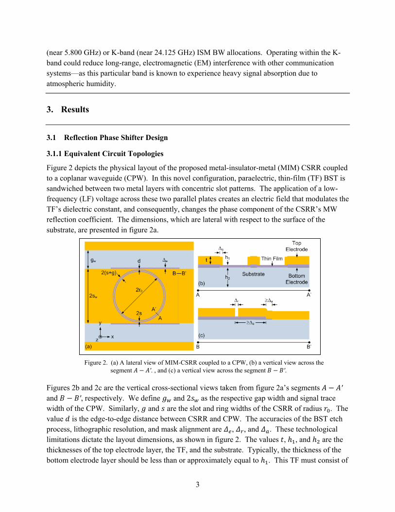
Figure 2 depicts the physical layout of the proposed metal-insulator-metal (MIM) CSRR coupled to a coplanar waveguide (CPW). In this novel configuration, paraelectric, thin-film (TF) BST is sandwiched between two metal layers with concentric slot patterns. The application of a low-frequency (LF) voltage across these two parallel plates creates an electric field that modulates the TF’s dielectric constant, and consequently, changes the phase component of the CSRR’s MW reflection coefficient. The dimensions, which are lateral with respect to the surface of the substrate, are presented in figure 2a.
Figure 2. (a) A lateral view of MIM-CSRR coupled to a CPW, (b) a vertical view across the segment ′. , and (c) a vertical view across the segment ′.
Figures 2b and 2c are the vertical cross-sectional views taken from figure 2a’s segments ′ and ′, respectively. We define and 2 as the respective gap width and signal trace width of the CPW. Similarly, and are the slot and ring widths of the CSRR of radius . The value is the edge-to-edge distance between CSRR and CPW. The accuracies of the BST etch process, lithographic resolution, and mask alignment are , , and . These technological limitations dictate the layout dimensions, as shown in figure 2. The values , , and are the thicknesses of the top electrode layer, the TF, and the substrate. Typically, the thickness of the bottom electrode layer should be less than or approximately equal to . This TF must consist of

4
titanium (Ti), platinum (Pt), or other very refractory metals, or conducting oxides, which will not diffuse into the BST TF during its furnace annealing process—which reaches temperatures near 700 °C. Conversely, the top electrode thick film should consist primarily of silver (Ag), gold (Au), copper (Cu), or another highly conductive metal, or alloy, in order to minimize MW power losses in the CPW and CSRR.
Figures 3a and 3b are the large- and small-signal equivalent circuits of a transponding detection node, respectively. In figure 3a, the MIM-CSRR is represented as an ideal varactor, denoted by
, connected in parallel with a resistor, , that models its leakage characteristics. The value is the real part of the terminating impedance, which is intentionally matched to the characteristic impedance, , of the CPW. A piezoelectric XDCR—which would be fabricated on the backside of the IC—converts its received acoustic signal into a LF voltage signal, which modulates the . The XDCR is MW-isolated from the resonator by high-impedance, radio frequency choke inductors (RFCs), physically realized with high-aspect-ratio through-wafer via holes. When the combined series resistance of the RFCs and MIM-CSRR is much greater than
, the voltage difference experienced by is approximately equal to that generated by the XDCR.
Figure 3. (a) LF large-signal equivalent circuit and (b) MW small-signal equivalent circuit.
In the small-signal model of figure 3b, an integrated antenna with an impedance matching network feeds a tunable, reflection phase-shifter consisting of a resonator-loaded CPW that is shunted to ground by the matched terminator. The phase-shifter relies on a novel MIM-CSRR as its reactive component. The MIM-CSRR is modeled by a simple inductor-resistor-capacitor (LRC) network whose EM coupling to the waveguide is represented by a transformer with an : 1 winding ratio. To use the MW small-signal model, we assume that the quiescent point of
is set in the LF large-signal model. Near the node’s unique on-resonant frequency, , (primarily determined by its value of ) most of the MW signal received from the antenna is perfectly reflected with a phase-shift controlled by . Outside the proximity of resonance, | |
, most of the incident MW power is absorbed by the termination impedance.

5
3.1.2 Reflection Phase-shifter Optimization
The expression | | · represents the reflection coefficient of the phase-shifter in terms of a magnitude, | |, and a phase, . By applying the principles of circuit theory, we have derived expressions for these quantities in terms of the circuit component values shown in the schematic of figure 3b. The expressions are as follows:
| | 1 · ; (1)
tan · . (2)
In these equations, we have used the coupling constant
, (3)
a previously defined, substituted variable (5) that is equivalent to the ratio of the isolated MIM-CSRR quality factor, , to that of the externally loaded device, . The resonant frequency of
the MIM-CSRR is defined as 2 √ . For the sake of mathematical convenience, it is
beneficial to keep in mind the relations: · and · , where ⁄ .
Ideally, the MIM-CSRR would yield negligible MW power loss; so, and consequently would both be infinite. Therefore, a first-order optimization of the reflection phase-shifter design involves determining an appropriate that maximizes the extreme values of both | | and . Because the -dependent trends of these quantities are inversely related to one another, a compromise is required.
For the optimization analysis, we define the ratio
/ (4)
and the averaged quantity 0 2⁄ . Here, is the maximum useable voltage magnitude allowed for the circuit design. If we design the circuit so that (and
1) for the on-resonant condition, , then the extremes of theta will be equal in magnitude, opposite in sign, and centered about 0. Additionally, we employ the previously defined (6) figure-of-merit (FOM) of paraelectric tunability:
· 100%. (5)
From equations 4 and 5, we find that the extremes of in terms of are
, 1%
, (6)

6
assuming that 0 . The variable is independent of m ( ), whereas and respectively, have direct and inverse proportionality to m ( √ · , and
, √⁄ ). Using these relations, equations 1 and 2 can be re-expressed in terms of
in the limit of ∞:
, lim , 1 1 · , ; (7)
, lim , tan 1 · , . (8)
A power series approximation of equation 8 can be found by calculating a third-order Taylor series expansion of with centered around 1:
, , 1 , 1 1 . (9)
From equations 7–9, we can define three additional FOMs that will aid our design. A reflection difference term
min , , ,
,· 100% (10)
expresses the maximum percentage deviation of the reflection magnitude from its on-resonant value. The quantity
, , · ° (11)
is the relative range of phase-shift values, and the quantity
, , (12)
is defined as the ratio of power series coefficients from equation 9, is an estimate of the linearity of ,∞ as a function of (or ). For our design, we wish to prioritize the constraint of .
The maximum allowable value of this FOM can be 10%. For an achievable value of 50%, we find 2 3⁄ and 4 3⁄ from equation 6. By asserting and solving for , ,
we can generate the corresponding values of and , as listed in table 1. Although, we wish to maximize , it is desirable to ensure linearity with respect to by keeping 1 if possible. We’ve determined , 0.7519 to be a suitable compromise for our application.

7
Table 1. FOMs for set values of , .
, % °
0.4275 1.000 16.22 0.0609
0.6092 2.000 22.96 0.1237
0.7519 3.000 28.14 0.1884
1.089 6.000 39.90 0.3952
1.453 10.00 51.68 0.7037
From equation 4, it is evident that is a function of . Its nonlinear dependence can derived from the paraelectric TF capacitance function (6) as
· 2 · cosh · sinh 2 1 , (13)
where 4 · 2 2 , which is the “2:1 voltage” corresponding to
the relation 0 2⁄ . For convenience, we set and 0 ⁄
1 100%⁄ . The extreme values of from equation 6 become and 0 . For the sake of reader visualization, we have used equation 13 to plot
equations 7 and 8 as functions of the normalized voltage / for 50%, as shown in figure 4.
From the plots of figure 4, we can infer that the reflection phase-shifter will modulate the incident MW signals with a response that is dependent on the rectified, LF, acoustic signal2 . This distortion arises from the even symmetry of the paraelectric TF capacitance
function (6). With a priori knowledge of the transponders’ responsive behaviors, it should be possible to compensate for these nonlinearities by intentionally introducing pre-distortion into the acoustic signal or by implementing a signal-processing-based linearization technique in the TxRx-DAQ. It would also be possible to eliminate the LF rectification, while optimizing sensitivity, by offsetting the quiescent point of the MIM-CSRR. Such a technique could be implemented by connecting a battery in series with the XDCR—although doing so would increase the unit cost of each node.
Figure 4. (a) ,∞ and (b) ,∞ versus / for different values of , .

8
3.1.3 Resonator Design
Figure 5 illustrates the EM field distributions across the segment of figure 2a. Figure 5a corresponds to the LF, large-signal electric field, which sets the quiescent point of the MIM-CSRR. The paraelectric TF situated in the gap, denoted by g, is biased entirely by fringe fields resulting from the LF voltage difference across the top and bottom electrode layers. However, the design of the MIM-CSRR entails calculating the resonant frequency based on the model of figure 3b. The component values ( and ) arise from the MW small-signal, electric, and magnetic field distributions depicted in figure 5b.
Figure 5. EM field distributions across segment . (a) LF large-signal, electric field (ELF). (b) MW small-signal, electric (EMW) and magnetic (HMW) fields.
We have calculated the effective values of and by modifying a previous analysis (7) for the case of a multilayered substrate. The magnetic field shown in figure 5b is symmetric with respect to the TF/air interface. It is uninfluenced by the inhomogeneity of permittivity, and exhibits the profile of a CPW’s alternating magnetic field. For this reason, the effective inductance of a CSRR can be calculated by computing 2 · 4⁄ , where is the per-unit-length inductance determined by conformal mapping analysis. The factor of is a characteristic of a CSRR configuration. The electric field of figure 5b is skewed away from the center of the MIM-CSRR. In the far-field, its profile is very similar to that due to a charged disk separated by an annular slot from a grounded, coplanar sheet with a multilayered substrate occupying the half-space below this conducting plane. So, the capacitance can be accurately estimated by applying the variational method to this similar scenario. In our calculations of and , we neglect to account for the presence of TF bottom electrode whose influence would only be perturbative. We justify this approximation by considering that most of the EM field distribution is concentrated in and around the coplanar gaps; the bottom electrode is recessed by a distance of at least from the lateral edges of the top electrode; the combined thickness of the

9
bottom electrode and paraelectric TF is typically less than one third the thickness of the top electrode; and the bottom electrode is a thin, high impedance parallel conductor whose influence is relatively small compared to that of the thick-film top electrode.
We used well-known formulae (8) to calculate the per-unit-length inductance,
3600 · · ⁄ , (14)
and the effective characteristic impedance,
,· , (15)
of the CSRR’s CPW-like slots. In these expressions, is the modulus of the complete elliptic integral of the first kind acting on the ratio . The effective dielectric constant, , accounts for the top electrode thickness, and is function of , the effective dielectric constant resulting
from a multilayered substrate (9). When designing the MIM-CSRR, we found it beneficial to compare the resulting radius to the guided wavelength,
, ·⁄ , (16)
where is the speed of light in free-space. Associated with this value is an attenuation constant
, which accounts for conductor and dielectric losses (8). Additionally, we have found that calculating the percentage of paraelectric TF’s contribution to yields an estimate of the
amount of MW EM energy occupying the TF. We’ve defined this FOM as
Υ · · 100%, (17)
where the quantity is the previously described filling factor (9). The value of Υ is important because it gives us an idea of how tunable the MIM-CSRR will be in comparison to its maximum possible limit, .
The design of the MIM-CSRR is constrained by technological limits. The utilization of standard TF processing techniques allows the thickness of the paraelectric layer, , to range from approximately 100 nm to about 1 µm. However, for a given biasing voltage range decreases with increasing . Our calculations have revealed that, as a rule of thumb, should be roughly equal to no greater than 10 times ; otherwise, Υ will be insignificant. Finally, the width of the bottom electrode strip, centered in figure 2b, must be and have an edge-to-edge tolerance of with respect to the top electrode strip. This condition limits minimization of the top electrode strip width, 2 2 . In our designs, we have assumed values that are conservative with respect to the tolerances of current state-of-art lithography systems ( 2.0 μm).

10
In table 2, we have listed calculated design parameters and corresponding FOMs for extracted physical quantities. The properties of the paraelectric BST TF are 90.0, tan 0.04, and 800 nm. Those of a sapphire substrate are 10.0, tan 1.00 10 , and
430 μm. The top electrode conductivity is 45.2 10 ·m and its thickness is 3.00 μm. We have selected an MIM-CSRR resonant frequency of 24.125 GHz, and a
typical number for the effective transformer winding 2. In section 2.2, we decided that
, 0.7519 is a suitable value for our application. We have equated a previous expression
and equation 15 to numerically solve for , for different values of :
, ·,
33.25 Ω. (18)
Table 2. MIM-CSRR design parameters and FOMs.
μm μm μm Np/μm %
6.000 2.913 4110. 6.929×10⁻⁶ 63.23
7.000 4.712 4210. 6.178×10⁻⁶ 57.73
7.555 6.000 4264. 5.795×10⁻⁶ 54.84
8.000 7.187 4306. 5.507×10⁻⁶ 52.61
9.000 10.35 4393. 4.930×10⁻⁶ 48.03
10.00 31.55 5780. 1.573×10⁻⁸ 0.000
Using the values of and , we have computed equations 16 and 17 to complete table 2.
From table 2, we see that minimizing the value of allows us to design a more compact and tunable device by virtue of the fact that and Υ, respectively, have direct and inverse proportionality to this variable. However, the effective attenuation constant also increases, which will result in a resonator with a lower Q. Therefore, a compromise is required. Since Υ rapidly diminishes to zero as is increased beyond ~9 µm, it is beneficial to keep the designed value of small enough (<8 µm), such that expected process variations would not cause the fabricated value of to cross this threshold. For this reason, we’ve chosen 7.6 μm and 2 6.0 μm for a more optimal configuration with respect to manufacturing considerations.
The final dimension is determined by finding a numerical solution for the equality:
2 · . We have used a previously defined integral
·· ·
(19)
for the capacitance function (7). We have also used a previously defined method (10) for determining a Green’s function specific to the multilayered substrate configuration:
1 . (20)

11
The calculated radius is 242.5 μm. The corresponding circumference is about one third of a guided wavelength; its diameter is less than one twenty-fifth the size of a free-space wavelength. A traditional ring resonator, composed of a single loop of transmission line, would have a circumference of multiple guided wavelengths. So, it is clear that the MIM-CSRR provides an ultra-compact solution. It has been previously pointed out that a complimentary spiral resonator (CSR) might allow for an additional factor of 2 in resonator size reduction. However, this configuration lacks the EM field cross-coupling of the CSRR; so, coupling the device to a CPW might be more challenging (7).
3.2 BST Research and Development
Figure 6a represents the configuration of the MIM varactors that were fabricated from 230-nm-thick BST thin films having compositions of Ba0.6Sr0.4TiO3. The unoptimized films were deposited on Si <100> substrates with blanket layers of Ti/Pt (approximately 200 nm in thickness) using a metal organic solution deposition (MOSD) technique. Immediately following this process, they were annealed in a conventional furnace at 700 °C and then UV-irradiated for 225 min, as described in references 11 and 12. Finally, 200-nm Au electrodes were placed over the sample using conventional optical lithography methods. This processing step defined both the top electrode and bottom electrode probe landing pads. The primary dimensions of concern of the varactors include diameter ( ), dielectric/metal overlap ( ), and signal-to-ground spacing ( ).
Figure 6. (a) Cross-sectional view BST-based MIM capacitor for MW characterizations. (b) Single-port MW reflection apparatus for characterizing electronic material properties (dielectric constant and loss tangent) at MW frequencies.
Figure 6b depicts the measurement scheme that was used for extracting material parameters from the test structures at microwave frequencies. The impedance values of the device under test (DUT) were extracted from the signal reflection data obtained from an Agilent E8364B PNA Series Network Analyzer. The reference plane (defined at 0) separates the apparatus from the DUT and was established using a short-open-load (SOL) calibration standard.
Figures 7a and b, respectively, represent tunability (τ) and dielectric loss tangent (tan ) as a function of externally applied DC bias voltage for different values of . Tunability is defined as 100% · / , where is the extracted capacitance and is the capacitance value

12
associated with zero voltage bias. For these characterizations, the and were fixed ( 15.0 μm and 50.0 μm) and was varied (22.4, 70.9, and 129. 5 µm). The values corresponding to the listed ’s were found to be 2.45, 20.1, and 62.0 pF, respectively. The impedance magnitudes of these values are respectively optimized (when
2 · · 50 Ω) for parameter extraction (with minimal error) at frequencies of 1.30 GHz, 158 MHz, and 51.3 MHz. For these measurements, an external voltage ranging from ‒12 to +12 V was applied to the sample through a biasing network. The samples were probed using 1-GHz test signals with power levels of ‒30 dBm. Interestingly, our data shows that increases and tan decreases as the device size is reduced. Further investigations are being conducted to draw solid conclusions regarding the physical mechanisms responsible for these phenomena.
Figure 7. (a) Tunability and (b) dielectric loss tangent vs. DC voltage bias for different electrode diameters.
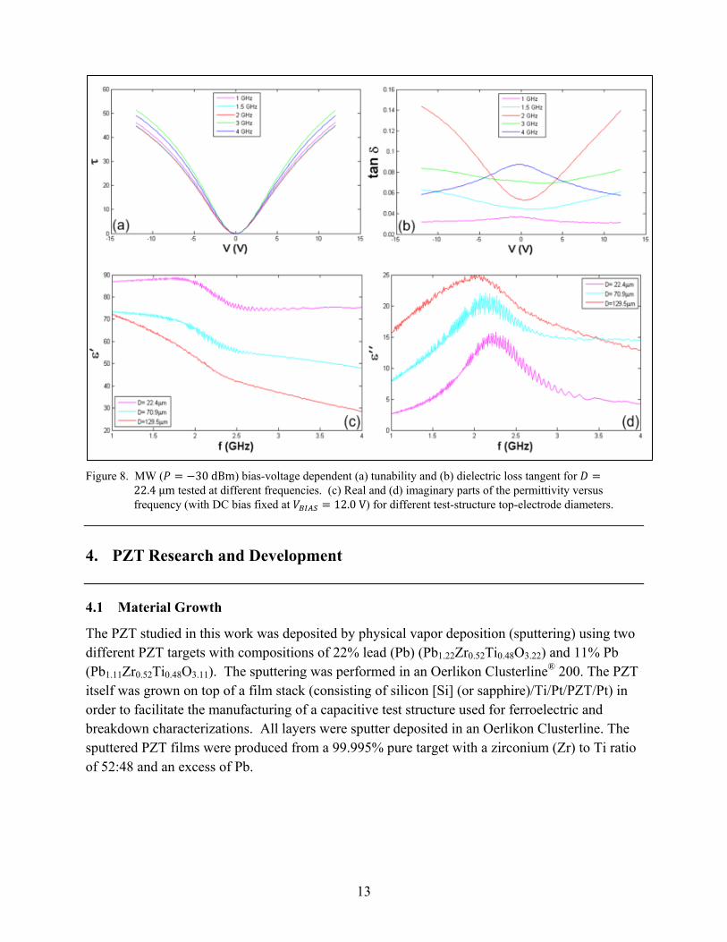
An unexpected phenomenon was observed in the high bias voltage regimes when using probing frequencies around 2 GHz. As shown in figures 8a and b, the tunability abruptly decreased while the dielectric loss tangent abruptly increased near a specific S-band frequency; these measurements were obtained from a test structure with a top electrode of 41.0 µm. From a wireless circuit designer’s point of view, this characteristic is undesirable. However, we decided to investigate this peculiarity for the sake of basic research. Figures 8c and 8d show frequency-dependent real and imaginary parts of the relative dielectric constant for MIM test structures with diameters of 22.4, 70.9, and 129.5 µm. These dispersion curves appear to obey a Kramers-Kronig relationship and are possibly indicative of a dipolar susceptibility mechanism (13) with a relaxation time inversely proportional to on-resonant frequency (~2.2 GHz). Investigators of recent works (14, 15) have attributed similar observations to electrostriction—an effect similar to piezoelectricity (16). Tappe et al. (15) has claimed that this resonances are only a function of the thin-film thickness; however, our observations suggest that enhancement of the resonance is a function of the device’s lateral dimensions. Further investigations will be required to draw solid conclusions regarding the physical mechanisms responsible for this loss characteristic.
13
Figure 8. MW ( 30 dBm) bias-voltage dependent (a) tunability and (b) dielectric loss tangent for 22.4 µm tested at different frequencies. (c) Real and (d) imaginary parts of the permittivity versus frequency (with DC bias fixed at 12.0 V) for different test-structure top-electrode diameters.
4. PZT Research and Development
4.1 Material Growth
The PZT studied in this work was deposited by physical vapor deposition (sputtering) using two different PZT targets with compositions of 22% lead (Pb) (Pb1.22Zr0.52Ti0.48O3.22) and 11% Pb (Pb1.11Zr0.52Ti0.48O3.11). The sputtering was performed in an Oerlikon Clusterline® 200. The PZT itself was grown on top of a film stack (consisting of silicon [Si] (or sapphire)/Ti/Pt/PZT/Pt) in order to facilitate the manufacturing of a capacitive test structure used for ferroelectric and breakdown characterizations. All layers were sputter deposited in an Oerlikon Clusterline. The sputtered PZT films were produced from a 99.995% pure target with a zirconium (Zr) to Ti ratio of 52:48 and an excess of Pb.

14
Ferroelectric data was acquired from the simple MIM capacitors, where the underlying Pt of described film stacks served as the bottom electrode. The top Pt electrode was patterned using a lift-off process. The mask used produced an array of 2.5 x 10‒3 cm2 squares (top electrodes). To expose the bottom electrode, a portion of the PZT was etched down to the underlying Pt film by use of a hydrochloric acid (HCl): hydrofluoric acid (HF): water (H2O) solution.
Remnant polarization was determined by use of a two point probe station. The probes were attached to a HP Agilent 4275A LCR Meter, which was controlled using a Radiant Technologies Charge 2.1 software package. X-ray diffraction (XRD) analysis was performed on Bruker General Area Detector Diffraction System (GADDS). Transmission electron microscopy (TEM) analysis was performed using a JEOL 2010F transmission electron microscope with an EDAX energy dispersive spectroscopy (EDS) attachment.
4.2 X-Ray Diffraction Studies
The XRD results, shown in figure 9, revealed that sputtered PZT films on both sapphire and Si substrates were textured along the [110] direction. The degree of preference for the [110] direction was greater in the sapphire substrate film, where the intensity of its corresponding peak was found to be larger compared to the intensity for the sputtered PZT on Si substrate. Overall, the PZT films on sapphire substrates were more oriented with all peaks present having higher intensities. Additionally, in the sputtered films, all reflections were comparatively low in intensity and were shifted with respect to the bulk PZT values as a result of film strain.
Figure 9. Powder diffraction results from PZT film patterns sputtered on (a) a sapphire substrate and (b) a Si
substrate.
4.3 TEM
High resolution transmission electron microscopy (HRTEM) analysis was performed on cross sections of sputtered PZT films on both Si and sapphire substrates. As both PZT samples displayed near identical TEM results, only one figure is presented. TEM selected area diffraction (SAD) data revealed the sputtered PZT films on both substrates were polycrystalline and had the perovskite structure, as shown in figures 10 and 11. Furthermore, the EDS data consistently showed that both films were Zr-rich with respect to Ti. A particularly noteworthy

15
aspect of these PZT samples was that they had a pronounced Pb concentration gradient near the surfaces of the films with maximum amounts of Pb at the air interface. It is suspected that during the annealing step of the PZT film fabrication, the crystallization process initiated at the Pt/PZT interfaces and propagated toward the surfaces. As the requisite amount of Pb was consumed, an excess may have been pushed upward which might have resulted in this residual Pb-rich region. An additional observation in support of this directional-crystallization hypothesis is the fact that the degree-of-crystallinity increased as a function of distance away from the surface of the material. A previous study on the same material system (17) has also identified the presence of an interfacial layer between the top electrodes of sputtered Pt/PZT/Ti/Pt type structures. Further investigation is required to better understand the formation of this layer. Nevertheless, the microstructural and crystalline quality of both films is comparable.
Figure 10. TEM image of PZT displaying film cross section along with Si substrate and SAD pattern.
Figure 11. TEM images of PVD deposited PZT displaying both low (a) and high (b) magnification of same sample on sapphire substrate.

16
4.4 Electrical Characterizations
Electrical test structures were prepared using PZT thin films with compositions of Pb1.22Zr0.52Ti0.48O3.22, and Pb1.11Zr0.52Ti0.48O3.11 that were deposited on c-plane sapphire wafers having metalized coatings consisting of 5 nm of Ti and 82 nm of Pt. Films with thicknesses of 300 and 600 nm were deposited using an Oerlikon CLC 200 Clusterline Sputter System. Following deposition, the films received a rapid thermal annealing (RTA) treatment at a temperature of 700 °C for a duration of 60 s. The device electrodes (as shown in figure 12a) were patterned using a combination of photolithography and ion milling techniques. Low-frequency characterizations were performed using a Radiant Technologies LCR meter and software package. Capacitors with zero bias values of approximately 14 and 7 nF were made from the 300- and 600-nm thick films, respectively—yielding an extracted permittivity in the neighborhood of 950. The DC leakage currents were found to be on the order of 150 nA. The dielectric polarization density versus DC bias voltage trace, shown as figure 12(b), revealed a remnant polarization of 39.7 μC · cm . Figure 12c shows a trace of capacitance density versus DC voltage bias for the cases of sweeping the bias from low-to-high and high-to-low values.
Figure 12. (a) Lateral-view of MIM PZT test structure. (b) Dielectric polarization density versus DC bias voltage. (c) Capacitance density versus DC voltage bias (sweep up and down).
The electric data are summarized in table 3, where the breakdown strength, leakage current, and resistivity are all displayed as a function of one another as well as the deposition conditions investigated. The breakdown voltages were determined from a collection of measurements taken from the same wafer to ensure accuracy of the value reported. As can be intuitively expected, a higher breakdown strength is correlated with a lower leakage current (and a correspondingly higher resistivity). The main point of interest, however, is the trend of increasing values of breakdown strength with reduction of excess Pb. A reduction of excess Pb in the sputter target by a factor of one-half (22% to 11%) resulted in an increase in the breakdown strength by more than a factor of two on Si substrates. The breakdown voltage of this PZT film was roughly 20% higher than that of the most optimized PVD-processed PZT (having 11% excess Pb and grown on sapphire substrates).

17
Table 3. Ferroelectric properties on Si and sapphire substrates.
Sample Pr,max
(µC/cm2) Leakage Current
(A) Resistivity
( m) Breakdown Voltage
(V) Target 22% Pb on Si 33.8 8.08×10⁻⁵ 2.5×10⁷ 10~20
Target 11% Pb on Si 31.8 7.69×10⁻⁹ 2.6×10¹¹ 30~50
Target 22% Pb on Sapphire 39.7 3.23×10⁻⁹ 5.4×10¹¹ 50~70
Target 11% Pb on Sapphire 37.3 1.62×10⁻⁹ 7.5×10¹¹ 60~80
When considering this material data in the context of integrated sensors, one must also consider the mechanisms of charge transport in PZT. In general terms, microstructure and the stoichiometry of both the crystalline and amorphous regions are the main contributors to said charge transport and therefore, by extension, the breakdown strength of PZT. Since these films are approximately 0.5 μm thick and breakdown occurs at relatively high fields, surface-related (ceramic metal contact band misalignment) phenomena will not be considered as a primary effect (18). Instead, we focus more on the bulk properties of the PZT itself. The bandgap of PZT is relatively low for a dielectric, with reported values of approximately 3.0 eV (19). It has been stated that PZT is intrinsically p-type due to the seemingly intrinsic presence of vacant Pb sites (20). Furthermore, it is commonly understood that oxygen vacancies in oxide-based ceramics created donor sites, which are n-type. From the crystallographic data, it is seen that the degree of crystallinity and PZT crystal quality improves when Pb is reduced from 22% to 11%. Since this reduction also correlates with higher breakdown strengths, it is possible that improved microstructure is a factor in improved breakdown strength. A point of interest is the possibility that the excess Pb may be assumed to limit the formation of Pb vacancies and therefore reduce the conductivity of the films. However, this mechanism was not directly observed. It is believed that the Pb played a crucial role in the PZT perovskite phase formation, where an excess decreased the quality of the crystal formation, paving the way for excessive oxygen vacancy and defect formation. The lower resistivity of the 22% excess Pb sample provided evidence for this supposition. Furthermore, though not quantified in this work, defect density in poorer quality crystals can become an issue at higher field strengths where trapped charges become elevated to the conduction band. These additional charges contribute to the total current through the device and ultimately the initiating mechanisms of material breakdown. Additional analysis of composition, defect density, and trap level are required to fully elucidate the mechanisms at work.
Variations in the ferroelectric properties of the conditions studied are displayed in table 3. There is a clear trend in increasing remnant polarization (37‒40 μC/cm2) and coercive field (50–80 kV/cm) on sapphire substrate, and 32–34 μC/cm2 and 10–50 kV/cm on Si substrate, respectively, as excess Pb is reduced in the PVD samples. What is not so evident is the mechanism by which the relative permittivity is affected by each of the deposition conditions. Within the PVD set though, the 11% excess Pb again produced the better result. The permittivity of a material results from polarization events. In ferroelectrics, this typically results from ionic

18
displacement. However, other mechanisms, such as internal barrier layers (IBLs) and charge collection at the contacts, can contribute as well. The culprit mechanism(s) in the case of this study were determined to be beyond the scope of this work but will be investigated in subsequent efforts. What can be asserted is that the PZT film on sapphire substrate yielded the highest remnant polarization and coercive field values, 39.7 μC/cm2 and 80 kV/cm, respectively, and the PVD condition with 11% excess Pb produced the highest relative permittivity, εr = 965.
5. Resistor Fabrication Results
5.1 Initial Sputtering Rate Characterizations
We have conducted a study involving the fabrication and characterization of thin-film nickel-chrome alloy (NiCr) resistors. Ultimately, these resistors will be used as the broadband impedance-matched terminators in the reflection phase-shifter circuits depicted in figure 3. In order to gauge a tolerance for our process variations, we have fabricated multiple structures with independent processing runs and measured their physical characteristics for repeatability. We have patterned the NiCr into the shape of van der Pauw cloverleaf-style test structures for the purpose of extracting sheet resistance using a standard four-point probe measurement technique. We have compared the estimated thickness extracted from these electrical measurements with the thicknesses measured using a scanning electron microscope (SEM) and Rutherford backscattering spectrometry (RBS). The RBS has also revealed a precise estimate of the Ni to chromium (Cr) ratio of NiCr alloy.
The metallization step was performed using a customized Denton Vacuum DV-502A sputtering system with a NiCr target reported by the manufacturer as having 99.9% purity (21). Our initial efforts to characterize the sputtering rates of our system involved depositing blanket layers of NiCr on two bare c-axis sapphire dies. The samples were sputtered independently of each other for durations of 4 min and 4 min, 20 s. A plasma power of 100 W was used in both cases with an argon (Ar) partial pressure of 2 mTorr. The NiCr thin-film thicknesses were determined using RBS and SEM measurements. Although the NiCr alloy composition was specified (by its manufacturer) as 80% Ni and 20% Cr (21), our RBS characterizations revealed the thin films to have a composition closer to 75% Ni and 25% Cr (22). The RBS characterization also revealed that the sample that received 4 min of sputtering had a thickness of 115 nm ± 0.5 nm, while the sample that received 4 min, 20 s of sputtering was 118 nm ± 0.5 nm. With the SEM imaging technique, the sample sputtered for 4 min was characterized as having a thickness of 125 nm ± 10 nm. Figure 13 shows an SEM micrograph of this NiCr thin film. The image is actually a composite of three blended images. The technique was applied for the purpose of gaining depth of field of the surface and finding an average thickness. These initial characterizations gave us a sputtering rate (~28.0 nm/min). This information would serve as a starting point for gauging the thin-film thickness as a function of sputtered deposition duration.

19
Figure 13. SEM composite micrograph of three blended images reveals an average NiCr thickness of (125 ± 10) nm. RBS characterization of the same sample measured the thickness as (115 ± 0.5) nm with an alloy composition of 75% Ni and 25% Cr.
Figure 14 shows a photograph of the NiCr test structures (van der Pauw cloverleafs and Hall Bars) fabricated using the method outlined previously. All electrical characterizations were performed using the largest van der Pauw cloverleaf. The area of this test structure’s square-shaped lamella is approximately 200 µm × 200 µm.
Figure 14. Photograph of NiCr (75/25) thin-film test structures on sapphire substrate for resistivity characterizations.
5.2 Sheet Resistance and Process Variation Characterizations
The accepted resistivity value of bulk NiCr (80/20)—commercially known as Nichrome—is 1.0 × 10⁻⁶ Ωm when measured at an ambient temperature of 20 °C (23). Other sources report that this value can vary from 1.0 × 10⁻⁶ Ωm to 1.5 × 10⁻⁶ Ωm (24). It is possible that this variation may be attributed to differences in the microstructural properties of the alloys. Perhaps, these differences arise in response to how the alloy is processed. Regardless, the goal of our electrical characterizations was not to simply measure the resistivity or sheet resistance, but to

20
gauge the tolerance of our process variations. From previous experience, we know that some microfabrication processing systems can be characterized with run-to-run deposition errors as high as 30%.
To accurately characterize resistivity and sheet resistance, we have used the van der Pauw method (25) in accordance with the standard ASTM F76-08 (26). This measurement method involves sourcing a current through two contacts of a prepared test sample and measuring the voltage drop across the remaining two. Because ideal voltage meters draw no current, four-point measurement techniques, in general, provide a means of measuring the sample resistivity without any influence from the test lead or sample contact resistances. In principle, the van der Pauw technique is topologically invariant—the technique will work on planar samples with arbitrary geometries. However, for proper execution, it requires a total of eight sourced-current-measured-voltage measurements. The calculated resistance for a current sourced through contacts labeled b and a and a voltage difference measured across contacts labeled c and d is denoted as: Rba,cd = Vcd / Iba. The eight measured resistances are then averaged according to equations 21 and 22:
, , , , /4 (21)
, , , , /4 (22)
The sheet resistance RS, expressed in units of Ω/, can be determined using equation 23:
⁄ ⁄ 1 (23)
To solve this expression, we processed the data using a customized script. We based our numerical code on an algorithm suggested by the National Institute of Standards and Technology (NIST) [27]. To find the material resistivity, one should simply multiply RS by the sample’s thickness d as shown in equation 24:
(24)
Figure 15 shows a depiction of our current measurement apparatus. Our characterization system uses an Agilent 4156C Precision Semiconductor Parameter Analyzer as the current source and voltage meter. An Agilent 34970A Data Acquisition Switch Unit with 34904A 4×8 Two-Wire Matrix Switch Module is used to switch the test leads for the eight required independent measurements of the van der Pauw method. The DUT is the van der Pauw cloverleaf configuration described in the previous section. Data acquisition and instrumentation automation is controlled using a custom Labview 8.5 Virtual Instrument (VI).

21
Figure 15. Apparatus for measuring sheet resistance using the van der Pauw method.
Three van der Pauw cloverleaves were prepared using three independent sputtering runs. Each NiCr (75/25) thin film was deposited for 2 min using the sputtering conditions described in the section 5.1 and 5.2.
All measurements were performed at the ambient room temperature, which was monitored to range between (19.7 and 19.8) °C ± 0.2 C. For a dissipated power per square of 10.0 µW/ , the sheet resistance of samples 1, 2, and 3 was measured as (16.56, 15.67 and 15.41) Ω/ , respectively. The mean and standard deviation of these three values are 15.88 Ω/ and 0.49 Ω/ , respectively. From this information, and without needing to know the actual NiCr thin-film thickness, we know that it should be possible to make a 50-Ω resistor with, at best, a 3.09% tolerance by using fabricating a rectangular thin film lamella that is approximately the length of 3.15 side-by-side squares (with a width equal to the length of one corresponding square). Additional data points are needed to find the point of convergence of the error tolerance. Assuming a sputtering rate of approximately 28 nm/min, we can estimate the thin-film thickness of the three samples as being close to 56 nm. Using equation 24, this estimate tells us that the resistivity of NiCr (75/25) thin films should be close to 0.9×10⁻⁶ Ωm when measured at a temperature of about 19.8 °C. This value is to 1.0 × 10⁻⁶ Ωm, the accepted resistivity value of bulk NiCr (80/20) when measured at a temperature of 20.0 °C (23).
Resistor tolerance can be reduced by increasing the manufacturing repeatability of the thin-film resistor thickness. Sputtering films of greater thickness will reduce the relative run-to-run variation of this value. For this reason, we plan to explore the possibility of sputtering thicker tantalum nitride (TaN) material, which has a lower value of resistivity than NiCr. Depositing TaN by a physical deposition method usually involves sputtering from a Ta source in an atmosphere of Ar and nitrogen gas (N2). However, the requirement of reproducing a specific gas ratio for each run might yield another significant source of processing error, which might also contribute in an adverse manner to resistor tolerance.
6. Metallized Through-wafer Microvia Results
A variety of through-wafer microvia holes have been drilled in c-plane sapphire substrates with thicknesses of 250 and 300 µm. The holes have been drilled so as to provide a substrate-
22
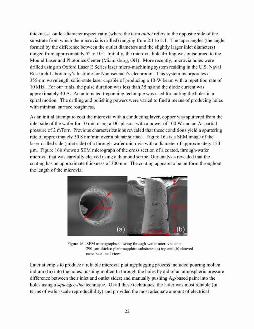
thickness: outlet-diameter aspect-ratio (where the term outlet refers to the opposite side of the substrate from which the microvia is drilled) ranging from 2:1 to 5:1. The taper angles (the angle formed by the difference between the outlet diameters and the slightly larger inlet diameters) ranged from approximately 5° to 10°. Initially, the microvia hole drilling was outsourced to the Mound Laser and Photonics Center (Miamisburg, OH). More recently, microvia holes were drilled using an Oxford Laser E Series laser micro-machining system residing in the U.S. Naval Research Laboratory’s Institute for Nanoscience’s cleanroom. This system incorporates a 355-nm wavelength solid-state laser capable of producing a 10-W beam with a repetition rate of 10 kHz. For our trials, the pulse duration was less than 35 ns and the diode current was approximately 40 A. An automated trepanning technique was used for cutting the holes in a spiral motion. The drilling and polishing powers were varied to find a means of producing holes with minimal surface roughness.
As an initial attempt to coat the microvia with a conducting layer, copper was sputtered from the inlet side of the wafer for 10 min using a DC plasma with a power of 100 W and an Ar partial pressure of 2 mTorr. Previous characterizations revealed that these conditions yield a sputtering rate of approximately 50.8 nm/min over a planar surface. Figure 16a is a SEM image of the laser-drilled side (inlet side) of a through-wafer microvia with a diameter of approximately 150 µm. Figure 16b shows a SEM micrograph of the cross section of a coated, through-wafer microvia that was carefully cleaved using a diamond scribe. Our analysis revealed that the coating has an approximate thickness of 300 nm. The coating appears to be uniform throughout the length of the microvia.
Figure 16. SEM micrographs showing through-wafer microvias in a 290-µm-thick c-plane sapphire substrate: (a) top and (b) cleaved cross-sectional views.
Later attempts to produce a reliable microvia plating/plugging process included pouring molten indium (In) into the holes; pushing molten In through the holes by aid of an atmospheric pressure difference between their inlet and outlet sides; and manually pushing Ag-based paint into the holes using a squeegee-like technique. Of all these techniques, the latter was most reliable (in terms of wafer-scale reproducibility) and provided the most adequate amount of electrical

23
conductance. However, current efforts are underway to modify other commercially available techniques used by the semiconductor industry.
7. Conclusions
We have presented a method of designing MIM-CSRR devices based on reliable formulae. The designed device is significantly smaller than traditional resonators operating at the same frequency. The reduced size is an enabling feature for producing inexpensive MW transponders fabricated in wafer-scale batches.
Initial characterizations of the BST TF provided us with a starting point for our first-order designs. K-band characterizations are currently in progress with the aid of smaller test structures. Our analytical method has provided significant insight regarding the fundamental performance limitations of our proposed topology. Further optimization of the design is being explored with the Mentor Graphics (Zeland) simulation tool IE3D.
BST has been characterized at MW frequencies. A bias-induced phenomenon possibly due to electrostriction has been observed at frequencies near 2.4 GHz. Since we are interested in using ISM BW allocations near this frequency, we will explore a means of mitigating this effect. Additionally, we plan to perform novel electrical characterization techniques that have relevance to our novel biasing scheme depicted in figure 5. We also plan to compare explore the use of sputtered BST as an alternative to the MOSD process.
It has been demonstrated that sputtered PZT film on a c-plane sapphire substrate has the great potential of taking advantage of PZT in a single chip to achieve inexpensive, fully integrated, passive, telemetric transponders. The data showed similar results in many aspects of the films investigated on both Si and sapphire substrates. In particular, for the 11% excess Pb target sputtered film, the breakdown voltage and ferroelectric data were significantly better than that of the 22% excess Pb target, which revealed a broad potential of the sputtered PZT film applications, especially on a sapphire substrate. PZT film depositions on both Si and sapphire substrates produced polycrystalline PZT with the perovskite structure and a [110] texture. PZT films on sapphire substrates possessed a greater degree of crystallinity than those on Si substrates. However, the higher Pb content proved beneficial for the reduction of remnant polarization. It is believed that further refinement of the production friendly sputtering process and subsequent device treatment will allow us to achieve better material performance.
Our research activities have included the implementation of fully integrated interconnect and resistor technologies. Initial successes have demonstrated the feasibility of devising a reliable technology to fabricate conductive fillings for microvia holes, as small as 50 µm in diameter, laser-drilled through a 250-µm-thick sapphire substrate. Our NiCr resistor efforts have produced suitable results for immediate implementation. However, in the second year of this project, we

24
will explore the possibility of using TaN as resistor material for the purpose of reducing resistance value tolerance.
Photolithography masks for CSRR and IDT structures have been designed. In the second year of this project, we plan to focus on fabricating and integrating these device technologies. Independent demonstrations of the functionalities of these devices will constitute complete academic studies. The full integration of these technologies will provide a solution that addresses a critical U.S. Army need.

25
8. References
1. Gil, I. et al. Varactor-loaded Split Rings Resonators for Tunable Notch Filters at Microwave Frequencies. Electron. Lett. 2004, 40, 1347.
2. Ozbay, E. et al. Ferroelectric Based Tuneable SRR Based Metamaterial for Microwave Applications. Proc. 37th Euro. Micro. Conf., 2007, 497–499.
3. Miranda, F.A. et al. Tunable Microwave Components for Ku- and K-band Satellite Communications. Integrated Ferroelect. 1998, 22, 789–797.
4. Kim, J. et al. CPW Bandstop Filter Using Slot-type SRRs. Electron. Lett. 2005, 41, 1333.
5. Pozar, D. M. Microwave Engineering; 2nd ed., John Wiley & Sons, Inc, 1998, pp. 648–652.
6. York, B. Tunable Dielectrics for RF Circuits. in Multifunctional Adaptive Microwave Circuits and Systems, M. Steer, Ed. Raleigh, NC:Scitech, 2009.
7. Baena, J. D. et al. Equivalent-Circuit Models for Split-Ring Resonators and Complementary Split-Ring Resonators Coupled to Planar Transmission Lines. IEEE Trans MTT 2005, 53, 1451–1461.
8. Wadell, B. C. Transmission Line Design Handbook; Artech House, Inc., Norwood, MA. 1991, 73–75.
9. Carlsson, E.; Gevorgian, S. S. IEEE Trans MTT 1999, 47, 1544–1552.
10. Chang, Y.; Chang, I. C. Electron. Lett. 1970, 6, 49–50.
11. Cole, M. W.; Ngo, E.; Tan, R.; Toonen, R. C.; Hirsch, S. G.; Ivill, M.; Hubbard, C.; Anthony, T. Low-cost Materials Processing Solution for Achieving Low Insertion Loss, Affordable Tunable Devices for Next Generation On-The-Move Communications Systems-Part II; ARL-TR-5227; U.S. Army Research Laboratory: Aberdeen Proving Ground, MD, June 2010.
12, Podpirka, A.; Cole, M. W.; Ramanathan, S. Appl. Phys. Lett. 2008, 92, 212906.
13. Balanis, C. A. Advanced Engineering Electromagnetics; Wiley, New York, 1989, pp. 73–84.
14. Morito, K.; Iwazkai, Y.; Suzuki, T.; Fujimoto, M. J. Appl. Phys. 2003, 94, 5199.
15. Tappe, S.; Bottger, U.; Wasser, R. Appl. Phys. Lett. 2004, 85, 624.
16. Mason, W. P. Phys. Rev.1948, 74, 1134.
26
17. Mamazza, Robert, Jr.; Mark, Nelson Y.; Polcawich, Ronald G.; Piekarski, Brett H.; Muralt, Paul; Reynolds, Glyn J. 15th IEEE International Symposium on the Applications of Ferroelectrics, Sunset Beach, NC, 314–317, 2006.
18. Cho, S. M.; Jeon, D. Y. Thin Solid Films 1999, 338, 149–154.
19. Sudhama, C.; Campbell, A. C.; Maniar, P. D.; Jones, R. E.; Moazzami, R.; Mogab, C. J.; Lee, J. C. J. Appl. Phy. 1993, 75 (2), 1014–1022.
20. Law, C. W.; Tong, K. Y.; Li, J. H.; Li, K. Solid-State Electronics 2000, 44, 1569–1571.
21. Item number EJTNICR304A2 from the Kurt J. Lesker Company.
22. Measurements (internally referenced as 120709) were reported by J.D. Demaree on December 7, 2009.
23. CRC Handbook of Chemistry and Physics, 65th ed., edited by R.C. Weast,CRC, Boca Raton, FL, 1985, p. E-78.
24. Conducting Materials - Microwave Encyclopedia - Microwaves101.com, http://www.microwaves101.com/encyclopedia/conducting.cfm . Nichrome - Wikipedia, the free encyclopedia, http://en.wikipedia.org/wiki/Nichrome . Resistivity of Nichrome, http://hypertextbook.com/facts/2007/HarveyKwan.shtml (accessed April 2011).
25. van der Pauw, L. J. Philips Res. Rep. 1958, 13, 1.
26. ASTM Standard F 76-08, Standard Test Methods for Measuring Resistivity and Hall Coefficient and Determining Hall Mobility in Single-Crystal Semiconductors, 2008 Annual Book of ASTM Standards (American Society for Testing Materials, West Conshohocken, PA, 2008).
27. IV. Algorithm Example. http://www.nist.gov/pml/semiconductor/hall.cfm (accessed April 2011).

27
9. Transitions
Knowledge presented in this report has resulted in a conference paper presented at the 27th Army Science Conference; a conference paper published in the Sensors and Transducers Journal; and a patent application (in development). We are currently exploring the possibility of a potential transition of the fully integrated system to the U. S. Army Aviation and Missile Research Development and Engineering Center.

28
List of Symbols, Abbreviations, and Acronyms
Ag silver
Ar argon
ARL U.S. Army Research Laboratory
Au gold
BST barium strontium titanate
BW bandwidth
COTS commercial off-the-shelf
CPW coplanar waveguide
Cr chromium
CSR complimentary spiral resonator
CSRR complementary SRR
Cu copper
DRI Director’s Research Initiative
DUT device under test
EDS energy dispersive spectroscopy
EM electromagnetic
FOM figure-of-merit
GADDS General Area Detector Diffraction System
H2O water
HCl hydrochloric acid
HF hydrofluoric acid
HFSS High Frequency Structure Simulator
HRTEM high resolution transmission electron microscopy
IBLs Internal Barrier Layers

29
IC Integrated Circuit
In indium
ISM Industrial, Scientific, and Medical
LF low-frequency
LRC inductor-resistor-capacitor
MIM metal-insulator-metal
MOSD metal organic solution deposition
MW microwave
N2 nitrogen gas
NDE non-destructive evaluation
NiCr nickel-chrome alloy
Pb lead
PM phase modulation
Pt platinum
PZT lead zirconate titanate
Qs quality factors
RBS Rutherford backscattering spectrometry
RFCs radio frequency choke inductors
RFID radio frequency infrared device
RTA rapid thermal annealing
SAD selected area diffraction
SEM Scanning Electron Microscope
Si silicon
SOL short-open-load
SRRs split ring resonators
TaN tantalum nitride
TEM transmission electron microscopy

30
Ti titanium
TF thin film
TxRx-DAQ transmitting/receiving data acquisition unit
VCO voltage controlled oscillator
VI Virtual Instrument
XDCR piezoelectric transducer
XRD x-ray diffraction
Zr zirconium

31
No. of Copies Organization 4 HCS US ARMY RSRCH LAB ATTN RDRL WMM E R TOONEN M P IVILL S GARY HIRSCH, M W COLE BLDG 4600 ABERDEEN PROVING GROUND MD 21005-5066 4 HCS US ARMY RSRCH LAB ATTN RDRL SEE-E R FU ATTN RDRL SEE G WOOD ATTN RDRL SEE E K ALIBERTI ATTN RDRL SED E T ZHELEVA 2800 POWDER MILL ROAD ADELPHI MD 20783-1197 TOTAL: 8 HCS

32
INTENTIONALLY LEFT BLANK.