a fully integrated materials framework for enabling the … diagram depicting the role an...
TRANSCRIPT
A Fully Integrated Materials Framework for Enabling the
Wireless Detection of Micro-defects in Aging and Battle-
worn Structures (Final Report)
by R. C. Toonen, S. G. Hirsch, R. X. Fu, M. P. Ivill, and M. W. Cole
ARL-MR-0822 May 2012
Approved for public release; distribution unlimited.

NOTICES
Disclaimers
The findings in this report are not to be construed as an official Department of the Army position
unless so designated by other authorized documents.
Citation of manufacturer’s or trade names does not constitute an official endorsement or
approval of the use thereof.
Destroy this report when it is no longer needed. Do not return it to the originator.
Army Research Laboratory Aberdeen Proving Ground, MD 21005
ARL-MR-0822 May 2012
A Fully Integrated Materials Framework for Enabling the
Wireless Detection of Micro-defects in Aging and Battle-
worn Structures (Final Report)
R. C. Toonen, S. G. Hirsch, R. X. Fu, M. P. Ivill, and M. W. Cole
Weapons and Materials Research Directorate, ARL
Approved for public release; distribution unlimited.

ii
REPORT DOCUMENTATION PAGE Form Approved OMB No. 0704-0188
Public reporting burden for this collection of information is estimated to average 1 hour per response, including the time for reviewing instructions, searching existing data sources, gathering and maintaining the
data needed, and completing and reviewing the collection information. Send comments regarding this burden estimate or any other aspect of this collection of information, including suggestions for reducing the
burden, to Department of Defense, Washington Headquarters Services, Directorate for Information Operations and Reports (0704-0188), 1215 Jefferson Davis Highway, Suite 1204, Arlington, VA 22202-4302.
Respondents should be aware that notwithstanding any other provision of law, no person shall be subject to any penalty for failing to comply with a collection of information if it does not display a currently valid
OMB control number.
PLEASE DO NOT RETURN YOUR FORM TO THE ABOVE ADDRESS.
1. REPORT DATE (DD-MM-YYYY)
May 2012
2. REPORT TYPE
DRI
3. DATES COVERED (From - To)
4. TITLE AND SUBTITLE
A Fully Integrated Materials Framework for Enabling the Wireless Detection of
Micro-defects in Aging and Battle-worn Structures (Final Report)
5a. CONTRACT NUMBER
5b. GRANT NUMBER
5c. PROGRAM ELEMENT NUMBER
6. AUTHOR(S)
R. C. Toonen, S. G. Hirsch, R. X. Fu, M. P. Ivill, and M. W. Cole
5d. PROJECT NUMBER
5e. TASK NUMBER
5f. WORK UNIT NUMBER
7. PERFORMING ORGANIZATION NAME(S) AND ADDRESS(ES)
U.S. Army Research Laboratory
ATTN: RDRL-WMM-E
Aberdeen Proving Ground, MD 21005
8. PERFORMING ORGANIZATION REPORT NUMBER
ARL-MR-0822
9. SPONSORING/MONITORING AGENCY NAME(S) AND ADDRESS(ES)
10. SPONSOR/MONITOR’S ACRONYM(S)
11. SPONSOR/MONITOR'S REPORT NUMBER(S)
12. DISTRIBUTION/AVAILABILITY STATEMENT
Approved for public release; distribution unlimited.
13. SUPPLEMENTARY NOTES
14. ABSTRACT
We present second-year results from a two-year study on a novel, inexpensive, passive, wireless solution for performing
nondestructive evaluation on the structural integrity of aging aircraft. Electro-mechanical resonant phenomena in barium
strontium titanate thin films have been thoroughly investigated using microwave reflectivity spectroscopy. Additionally,
piezoelectric lead zirconate titanate thin films have been electrically characterized in terms of capacitance and dielectric loss
tangent. Finally, we have explored the integration of such devices into a detection system involving piezoelectric wafer active
transducers.
15. SUBJECT TERMS
barium strontium titanate, lead zirconate titanate, microwave dielectric spectroscopy, third-order nonlinear susceptibility
16. SECURITY CLASSIFICATION OF: 17. LIMITATION OF ABSTRACT
UU
18. NUMBER OF PAGES
34
19a. NAME OF RESPONSIBLE PERSON
R. C. Toonen a. REPORT
Unclassified
b. ABSTRACT
Unclassified
c. THIS PAGE
Unclassified
19b. TELEPHONE NUMBER (Include area code)
(410) 306-4536
Standard Form 298 (Rev. 8/98)
Prescribed by ANSI Std. Z39.18
iii
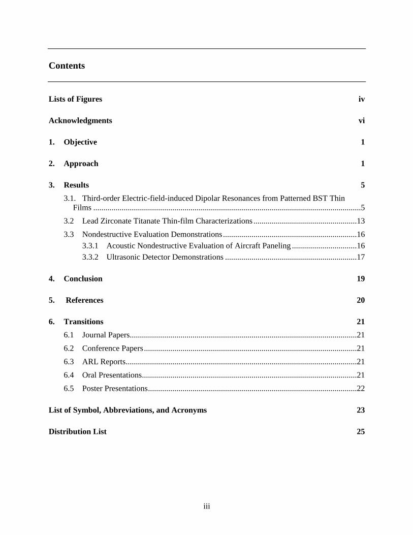
Contents
Lists of Figures iv
Acknowledgments vi
1. Objective 1
2. Approach 1
3. Results 5
3.1. Third-order Electric-field-induced Dipolar Resonances from Patterned BST Thin
Films ....................................................................................................................................5
3.2 Lead Zirconate Titanate Thin-film Characterizations ...................................................13
3.3 Nondestructive Evaluation Demonstrations ..................................................................16
3.3.1 Acoustic Nondestructive Evaluation of Aircraft Paneling ................................16
3.3.2 Ultrasonic Detector Demonstrations .................................................................17
4. Conclusion 19
5. References 20
6. Transitions 21
6.1 Journal Papers................................................................................................................21
6.2 Conference Papers .........................................................................................................21
6.3 ARL Reports..................................................................................................................21
6.4 Oral Presentations..........................................................................................................21
6.5 Poster Presentations .......................................................................................................22
List of Symbol, Abbreviations, and Acronyms 23
Distribution List 25
iv
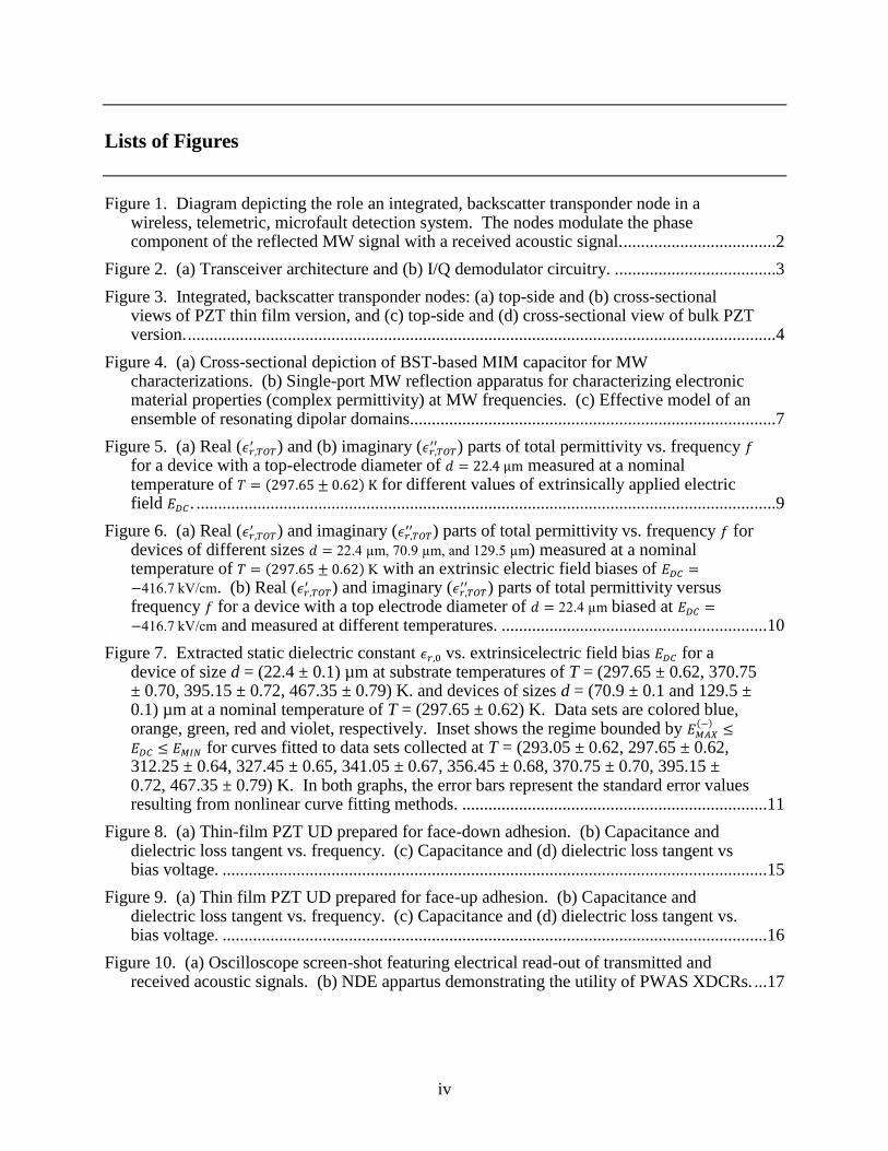
Lists of Figures
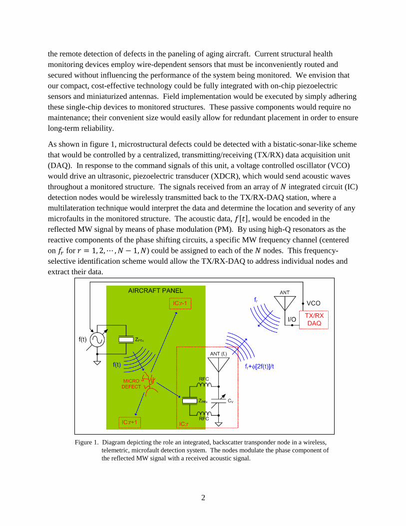
Figure 1. Diagram depicting the role an integrated, backscatter transponder node in a wireless, telemetric, microfault detection system. The nodes modulate the phase component of the reflected MW signal with a received acoustic signal. ...................................2
Figure 2. (a) Transceiver architecture and (b) I/Q demodulator circuitry. .....................................3
Figure 3. Integrated, backscatter transponder nodes: (a) top-side and (b) cross-sectional views of PZT thin film version, and (c) top-side and (d) cross-sectional view of bulk PZT version. .......................................................................................................................................4
Figure 4. (a) Cross-sectional depiction of BST-based MIM capacitor for MW characterizations. (b) Single-port MW reflection apparatus for characterizing electronic material properties (complex permittivity) at MW frequencies. (c) Effective model of an ensemble of resonating dipolar domains....................................................................................7
Figure 5. (a) Real ( ) and (b) imaginary (
) parts of total permittivity vs. frequency for a device with a top-electrode diameter of measured at a nominal temperature of for different values of extrinsically applied electric field . .....................................................................................................................................9
Figure 6. (a) Real ( ) and imaginary (
) parts of total permittivity vs. frequency for devices of different sizes m m and m) measured at a nominal temperature of with an extrinsic electric field biases of
cm. (b) Real ( ) and imaginary (
) parts of total permittivity versus frequency for a device with a top electrode diameter of m biased at
cm and measured at different temperatures. .............................................................10
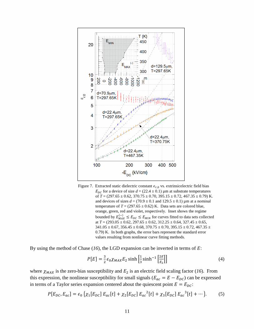
Figure 7. Extracted static dielectric constant vs. extrinsicelectric field bias for a device of size d = (22.4 ± 0.1) µm at substrate temperatures of T = (297.65 ± 0.62, 370.75 ± 0.70, 395.15 ± 0.72, 467.35 ± 0.79) K. and devices of sizes d = (70.9 ± 0.1 and 129.5 ± 0.1) µm at a nominal temperature of T = (297.65 ± 0.62) K. Data sets are colored blue, orange, green, red and violet, respectively. Inset shows the regime bounded by
for curves fitted to data sets collected at T = (293.05 ± 0.62, 297.65 ± 0.62, 312.25 ± 0.64, 327.45 ± 0.65, 341.05 ± 0.67, 356.45 ± 0.68, 370.75 ± 0.70, 395.15 ± 0.72, 467.35 ± 0.79) K. In both graphs, the error bars represent the standard error values resulting from nonlinear curve fitting methods. ......................................................................11
Figure 8. (a) Thin-film PZT UD prepared for face-down adhesion. (b) Capacitance and dielectric loss tangent vs. frequency. (c) Capacitance and (d) dielectric loss tangent vs bias voltage. .............................................................................................................................15
Figure 9. (a) Thin film PZT UD prepared for face-up adhesion. (b) Capacitance and dielectric loss tangent vs. frequency. (c) Capacitance and (d) dielectric loss tangent vs. bias voltage. .............................................................................................................................16
Figure 10. (a) Oscilloscope screen-shot featuring electrical read-out of transmitted and received acoustic signals. (b) NDE appartus demonstrating the utility of PWAS XDCRs. ...17
v
Figure 11. Face-down experiment: (a) test configuration and (b) transfer functions of PWAS and the thin-film PZT UD. .......................................................................................................18
Figure 12. Face-up experiment: (a) test configuration and (b) transfer function of the thin-film PZT UD. ...........................................................................................................................19
vi
Acknowledgments
We thank Eric H. Ngo and Clifford W. Hubbard for their general technical support. We also
thank Tsvetanka S. Zheleva for transmission electron microscopy (TEM) inspection and J. Derek
Demaree for Rutherford backscattering spectrometry (RBS) analysis. We thank Edmond T.
Elburn (North East High School/George Washington University (GWU)-Department of Defense
(DoD) Student and Engineering Apprentice Program) and Nagid Brown (University of the
Virgin Islands/National Science Foundation) for their technical assistance with lead zirconate
titanate (PZT) device implementation, and Victor Lee (University of Michigan-Ann Arbor) and
Theo Anthony for help with electromagnetic simulations.
1
1. Objective
The objective of this body of work is to explore, develop, and demonstrate the feasibility of
providing the U.S. Army with inexpensive, scalable, passive, and ultra-low power consuming
fully integrated circuits that enable analog information from a piezoelectric sensor to be
telemetrically monitored via a radio frequency identification (RFID)-like backscatter
transponder. First-year technical progress from a two-year U.S. Army Research Laboratory
(ARL) Director’s Research Initiative (DRI) sponsored project entitled “A Fully Integrated
Materials Framework for Enabling the Wireless Detection of Micro-Defects in Aging and Battle-
Worn Structures” was reported in ARL Memorandum Report, ARL-MR-0775 (1). The first-year
results presented in that report include reflection phase shifter design and optimization; initial
growth studies and characterizations of barium strontium titanate (BST) and lead zirconate
titanate (PZT) thin films; thin-film nickel chromium alloy (NiCr) resistor fabrication and testing;
and progress towards realizing plated, laser-drilled, through-wafer microvias in sapphire
substrates.
In this report, we present technical results from the second-year study, which primarily focused
on characterizing and understanding of the physical properties of the BST and PZT thin films.
Using microwave reflection spectroscopy, the complex permittivities of etch defined, 240-nm-
thick, (Ba0.6Sr0.4)TiO3 thin films were measured over the frequency range of (1 to 4) GHz.
Anomalous electric-field-induced electro-acoustic resonances were observed and characterized
as a function of extrinsic electric field magnitude, ambient temperature, and sample diameter.
The real and imaginary parts of the measured permittivities were fit to frequency-dependent
functions derived from the Lorentz oscillator model. From these functions, extracted static
dielectric constants were found to display excellent agreement with a closed-form expression
derived by calculating third-order nonlinear susceptibility from the Landau-Devonshire-Ginzberg
model. Finally, the electrical properties of sputtered Pb1+y[ZrxTi1–x]O3+y (PZT) thin films were
studied in terms of frequency- and voltage-dependent capacitance and dielectric loss tangent
measurements. Preliminary experiments related to defect detection in aircraft-grade aluminum
(Al) panels were demonstrated using both thin-film and bulk PZT.
2. Approach
There is a critical military need to develop the technology of fully integrated, passive telemetric
readout systems. Remote sensors accessed via microwave (MW) transponders could allow for a
new and improved means of wirelessly characterizing system properties for the purpose of
nondestructive evaluation (NDE). One of the many applications of this potential innovation is
2
the remote detection of defects in the paneling of aging aircraft. Current structural health
monitoring devices employ wire-dependent sensors that must be inconveniently routed and
secured without influencing the performance of the system being monitored. We envision that
our compact, cost-effective technology could be fully integrated with on-chip piezoelectric
sensors and miniaturized antennas. Field implementation would be executed by simply adhering
these single-chip devices to monitored structures. These passive components would require no
maintenance; their convenient size would easily allow for redundant placement in order to ensure
long-term reliability.
As shown in figure 1, microstructural defects could be detected with a bistatic-sonar-like scheme
that would be controlled by a centralized, transmitting/receiving (TX/RX) data acquisition unit
(DAQ). In response to the command signals of this unit, a voltage controlled oscillator (VCO)
would drive an ultrasonic, piezoelectric transducer (XDCR), which would send acoustic waves
throughout a monitored structure. The signals received from an array of integrated circuit (IC)
detection nodes would be wirelessly transmitted back to the TX/RX-DAQ station, where a
multilateration technique would interpret the data and determine the location and severity of any
microfaults in the monitored structure. The acoustic data, , would be encoded in the
reflected MW signal by means of phase modulation (PM). By using high-Q resonators as the
reactive components of the phase shifting circuits, a specific MW frequency channel (centered
on for ) could be assigned to each of the nodes. This frequency-
selective identification scheme would allow the TX/RX-DAQ to address individual nodes and
extract their data.
Figure 1. Diagram depicting the role an integrated, backscatter transponder node in a wireless,
telemetric, microfault detection system. The nodes modulate the phase component of
the reflected MW signal with a received acoustic signal.
3
An advantage of using PM to transmit analog data across a short range is that this
communication scheme is robust against calibration drift due to atmospheric signal attenuation.
Traditionally, the military has reserved the L-band, (1 to 2) GHz, for telemetry. There is a strong
interest within the wireless community to develop miniaturized, passive S-band transponders
(specifically operating in the frequency range of 2.400 to 2.500 GHz) due to the industrial,
scientific, and medical (ISM) bandwidth (BW) allocations. However, because our technology is
frequency-scalable, the short-range data link needed for our application could reside in C-band
(near 5.800 GHz) or K-band (near 24.125 GHz) ISM BW allocations. Operating within the K-
band could reduce long-range, electromagnetic (EM) interference with other communication
systems—as this particular band is known to experience heavy signal absorption due to
atmospheric humidity.
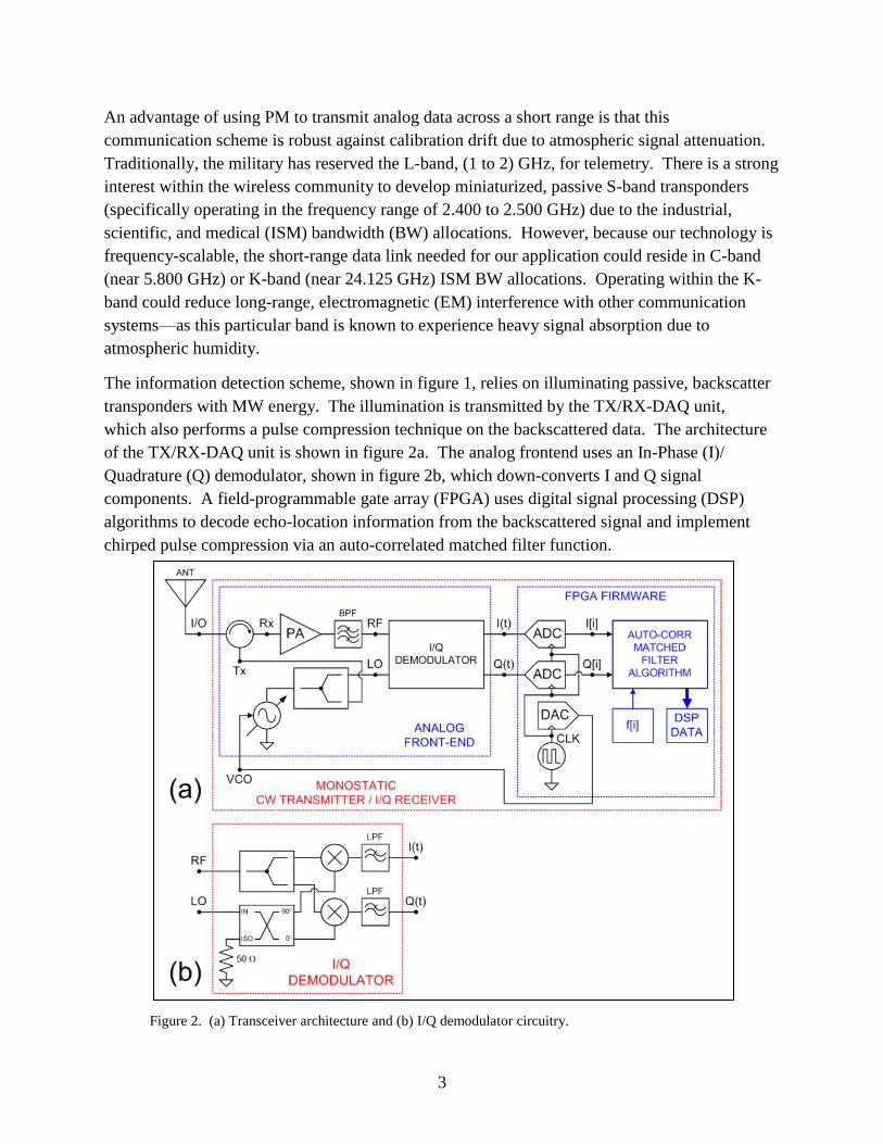
The information detection scheme, shown in figure 1, relies on illuminating passive, backscatter
transponders with MW energy. The illumination is transmitted by the TX/RX-DAQ unit,
which also performs a pulse compression technique on the backscattered data. The architecture
of the TX/RX-DAQ unit is shown in figure 2a. The analog frontend uses an In-Phase (I)/
Quadrature (Q) demodulator, shown in figure 2b, which down-converts I and Q signal
components. A field-programmable gate array (FPGA) uses digital signal processing (DSP)
algorithms to decode echo-location information from the backscattered signal and implement
chirped pulse compression via an auto-correlated matched filter function.
Figure 2. (a) Transceiver architecture and (b) I/Q demodulator circuitry.
4
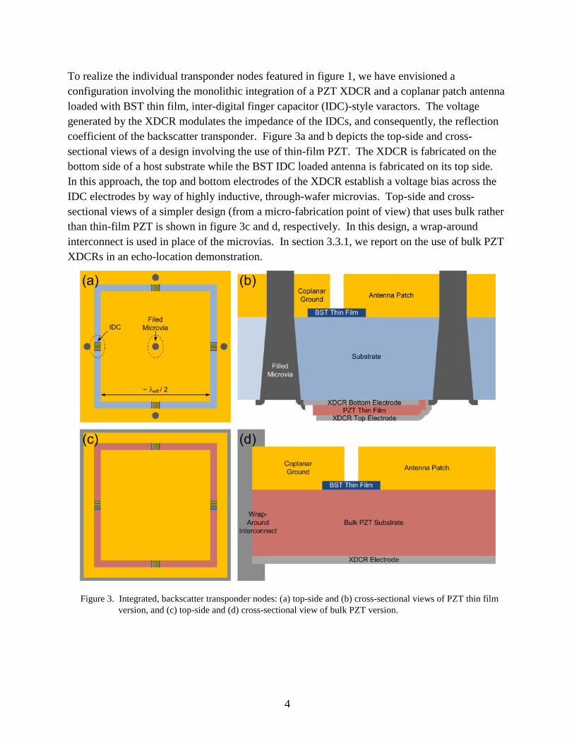
To realize the individual transponder nodes featured in figure 1, we have envisioned a
configuration involving the monolithic integration of a PZT XDCR and a coplanar patch antenna
loaded with BST thin film, inter-digital finger capacitor (IDC)-style varactors. The voltage
generated by the XDCR modulates the impedance of the IDCs, and consequently, the reflection
coefficient of the backscatter transponder. Figure 3a and b depicts the top-side and cross-
sectional views of a design involving the use of thin-film PZT. The XDCR is fabricated on the
bottom side of a host substrate while the BST IDC loaded antenna is fabricated on its top side.
In this approach, the top and bottom electrodes of the XDCR establish a voltage bias across the
IDC electrodes by way of highly inductive, through-wafer microvias. Top-side and cross-
sectional views of a simpler design (from a micro-fabrication point of view) that uses bulk rather
than thin-film PZT is shown in figure 3c and d, respectively. In this design, a wrap-around
interconnect is used in place of the microvias. In section 3.3.1, we report on the use of bulk PZT
XDCRs in an echo-location demonstration.
Figure 3. Integrated, backscatter transponder nodes: (a) top-side and (b) cross-sectional views of PZT thin film
version, and (c) top-side and (d) cross-sectional view of bulk PZT version.
5
3. Results
3.1 Third-order Electric-field-induced Dipolar Resonances from Patterned BST Thin
Films
There is currently a strong interest within the wireless community to develop low power-loss
varactor technologies that can be used for S-band operation—specifically, within the frequency
range of (2.400 to 2.500) GHz due to the ISM bandwidth allocations. Such tunable components
are sought for use in antenna, transponder, and front-end systems that require agile frequency
selectivity or impedance matching optimization. In order to improve the performance of these
systems, it is important to fully understand the nature of physical phenomena that give rise to
undesired power loss. This section describes the observed electric-field-induced loss
mechanisms of thin-film (Ba0.6Sr0.4)TiO3 (BST) varactors that reside within the aforementioned
frequency band. By investigating how such loss mechanisms behave in response to external
stimuli, we have gained insight with respect to how these effects can be reduced or even
eliminated. It is also possible that such loss mechanisms could be exploited for the purpose of
engineering super-compact, high quality factor, frequency-selective filters.
Previous studies have reported on similar resonant loss mechanisms in paraelectric phase
strontium titanate (SrTiO3) (2, 3) and (Ba0.7Sr0.3)TiO3 (3–5). Such anomalies have been
attributed to electric-field-induced piezoelectricity (2), electrostrictivity (4), and a combination of
these two mechanisms (3, 5). Some of these studies (3, 4) have shown that models based on
acoustic impedance calculations yield predictions that qualitatively agree with observed
behavior; however, no attempts have been made to accurately model the lineshape of the
anomalous resonances in order to extract physical information. We have shown that profiles of
such signatures can be precisely fit to simple expressions derived from the Lorentz oscillator
model. We have also shown that the extracted dielectric constant has third-order dependence on
extrinsic electric field and exhibits excellent agreement with a model derived from a Landau-
Devonshire-Ginzberg (LDG) power series expansion.
As depicted in figure 4a, metal-insulator-metal (MIM) varactors were fabricated from BST thin
films with measured thicknesses of and having compositions of
Ba0.6Sr0.4TiO3. The films were grown via the metal organic solution deposition (MOSD)
technique using carboxylate-alkoxide precursors. A detailed description of the MOSD precursor
solution preparation and film deposition technique has been previously reported (6). The BST
films were deposited on platinum (Pt) blanket layers (with nominal thicknesses of 200 nm)
adhered to 300-µm-thick c-plane sapphire (Al2O3) substrates with thin titanium adhesion layers
(of approximately 40 nm in thickness). In the presence of flowing oxygen, the BST films were
crystallized using conventional furnace annealing (CFA) at a temperature of 750 °C for a
duration of 60 min. Following the CFA process, these films were ultraviolet (UV)-irradiated for
6
225 min in an oxygen atmosphere held at a temperature of 700 °C, as described in previously
published literature (7). The BST thin films were then lithographically masked with Microposit
SC-1827 photoresist and etched with buffered oxide etchant (5:1:ammonium fluoride
[NH4F]:hydrofluoric acid [HF]). Finally, 200-nm-thick gold electrodes were sputtered over the
etch-defined patches of BST and patterned using conventional optical lithography and lift-off
methods. This processing step defined both the top electrode and bottom electrode probe landing
pads. The primary dimensions of concern of the varactors include diameter , dielectric/metal
overlap LOV, and signal-to-ground spacing LSP. For the characterizations presented in this study,
values of LOV = (15.0 ± 2.0) µm and LSP = (50.0 ± 0.05) µm were held fixed for each
measurement; the accuracies of these two values are due to mask alignment error and optical
lithography mask resolution, respectively. The parameter was used as a variable in our
experiments and took on values of (22.4, 70.9, and 128.95) µm ± 0.1 µm. These values were
chosen so as to minimize network analyzer error by satisfying the relationship:
where is the measured device under test (DUT) impedance magnitude,
is test signal frequency, and is the extracted DUT capacitance.
Figure 4b illustrates the measurement scheme that was used for extracting material parameters
from the test structures at MW frequencies. The DUT impedance values were measured using
MW reflection spectrometry obtained from an Agilent Technologies E8364C PNA Series
network analyzer, as illustrated in figure 4b. The DUT was contacted using a GGB Industries
model 50A-GS-150-P high performance MW probe. The fictitious reference plane (defined at
), which separates the apparatus from the DUT, was established using a set of short-open-
load (SOL) standards from a GGB Industries CS-8 calibration substrate. A DC voltage ( )
was established across the top and bottom electrodes, using an Agilent Technologies PNA
Option UNL bias-tee and a Yokogawa 7651 programmable DC source, for the purpose of
biasing the BST thin film with an extrinsic electric field ( ). In all reported
experiments, the MW small-signal power level was held fixed at a value of ‒3 dBm. When
extracting the real part of the relative permittivity, we have used the approximation
. This assumption, which neglects the influence of fringe field on the
measured value of , is appropriate (8) because, for each characterized DUT, .
Likewise, we have extracted the imaginary part of the relative permittivity using the
approximation
, where is the measured dielectric loss tangent. The
accuracy of the reported relative permittivity values can be readily calculated assuming the
capacitance, diameter, and film thickness measurements are entirely independent of one
another—allowing for all covariant terms to vanish (9). In our measurements, the error term
associated with the capacitance measurement is considerably smaller than those of the diameter
and film thickness measurements, yielding the approximation
.
7
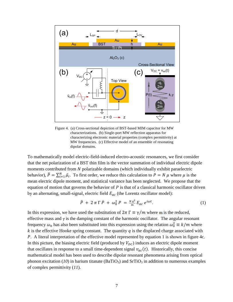
Figure 4. (a) Cross-sectional depiction of BST-based MIM capacitor for MW
characterizations. (b) Single-port MW reflection apparatus for
characterizing electronic material properties (complex permittivity) at
MW frequencies. (c) Effective model of an ensemble of resonating
dipolar domains.
To mathematically model electric-field-induced electro-acoustic resonances, we first consider
that the net polarization of a BST thin film is the vector summation of individual electric dipole
moments contributed from polarizable domains (which individually exhibit paraelectric
behavior), . To first order, we reduce this calculation to where is the
mean electric dipole moment, and statistical variance has been neglected. We propose that the
equation of motion that governs the behavior of is that of a classical harmonic oscillator driven
by an alternating, small-signal, electric field (the Lorentz oscillator model):
. (1)
In this expression, we have used the substitution of where is the reduced,
effective mass and is the damping constant of the harmonic oscillator. The angular resonant
frequency has also been substituted into this expression using the relation where
is the effective Hooke spring constant. The quantity is the displaced charge associated with
. A literal interpretation of the effective model represented by equation 1 is shown in figure 4c.
In this picture, the biasing electric field (produced by ) induces an electric dipole moment
that oscillates in response to a small time-dependent signal . Historically, this concise
mathematical model has been used to describe dipolar resonant phenomena arising from optical
phonon excitation (10) in barium titanate (BaTiO3) and SrTiO3 in addition to numerous examples
of complex permittivity (11).
8
By solving equation 1 and applying the relations for complex electric susceptibility and
permittivity— and , respectively—we derive
expressions for the real part of :
(2)
and its imaginary counterpart:
. (3)
These expressions are given in terms of the normalized frequency . For practical
purposes, we use cyclic frequency ( , expressed in units of GHz) rather than angular
frequency. The other substituted variables include the dimensionless quantities of the DC static
dielectric constant ( ) and the ratio which asymptotically approaches
a quantity commonly known as the quality factor— for where is the full
width at half maximum of the resonant lineshape. As expected from the Lorentz model,
where which is the square of the quantity historically
known as the plasma frequency for the case of a free ionized gas (i.e., and ).
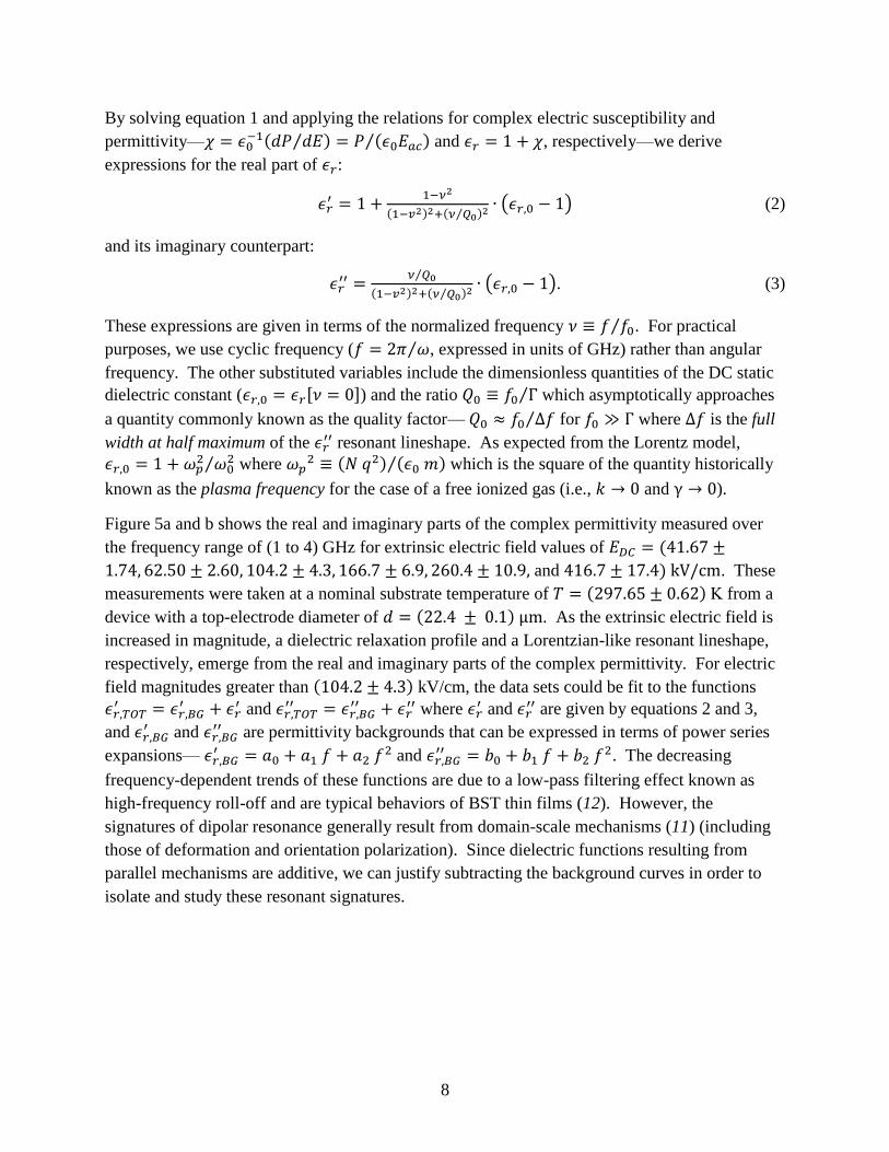
Figure 5a and b shows the real and imaginary parts of the complex permittivity measured over
the frequency range of (1 to 4) GHz for extrinsic electric field values of
and . These
measurements were taken at a nominal substrate temperature of from a
device with a top-electrode diameter of . As the extrinsic electric field is
increased in magnitude, a dielectric relaxation profile and a Lorentzian-like resonant lineshape,
respectively, emerge from the real and imaginary parts of the complex permittivity. For electric
field magnitudes greater than kV/cm, the data sets could be fit to the functions
and
where and
are given by equations 2 and 3,
and and
are permittivity backgrounds that can be expressed in terms of power series
expansions—
and
. The decreasing
frequency-dependent trends of these functions are due to a low-pass filtering effect known as
high-frequency roll-off and are typical behaviors of BST thin films (12). However, the
signatures of dipolar resonance generally result from domain-scale mechanisms (11) (including
those of deformation and orientation polarization). Since dielectric functions resulting from
parallel mechanisms are additive, we can justify subtracting the background curves in order to
isolate and study these resonant signatures.
9
Figure 5. (a) Real ( ) and (b) imaginary (
) parts of total permittivity vs. frequency for a device
with a top-electrode diameter of measured at a nominal temperature of for different values of extrinsically applied electric field .
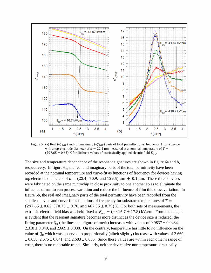
The size and temperature dependence of the resonant signatures are shown in figure 6a and b,
respectively. In figure 6a, the real and imaginary parts of the total permittivity have been
recorded at the nominal temperature and curve-fit as functions of frequency for devices having
top electrode diameters of and . These three devices
were fabricated on the same microchip in close proximity to one another so as to eliminate the
influence of run-to-run process variation and reduce the influence of film thickness variation. In
figure 6b, the real and imaginary parts of the total permittivity have been recorded from the
smallest device and curve-fit as functions of frequency for substrate temperatures of
. For both sets of measurements, the
extrinsic electric field bias was held fixed at cm. From the data, it
is evident that the resonant signature becomes more distinct as the device size is reduced; the
fitting parameter (the lineshape figure of merit) increases with values of 0.9837 ± 0.0434,
2.318 ± 0.049, and 2.669 ± 0.038. On the contrary, temperature has little to no influence on the
value of which was observed to proportionally (albeit slightly) increase with values of 2.669
± 0.038, 2.675 ± 0.041, and 2.683 ± 0.036 Since these values are within each other’s range of
error, there is no reportable trend. Similarly, neither device size nor temperature drastically
10
influenced the value of . For increasing device size, the values of were measured as (2.495
±0.002, 2.391 ± 0.004, and 2.409 ± 0.039) GHz. For increasing temperature, the values of
were found to be: (2.495 ± 0.002, 2.522 ± 0.002, and 2.510 ± 0.002) GHz. Previous studies
have shown that the value of is primarily governed by thin-film thickness (4).
Figure 6. (a) Real ( ) and imaginary (
) parts of total permittivity vs. frequency for devices
of different sizes m m and m) measured at a nominal temperature of
with an extrinsic electric field biases of cm. (b)
Real ( ) and imaginary (
) parts of total permittivity versus frequency for a device
with a top electrode diameter of m biased at cm and measured at
different temperatures.
In figure 7, the extracted fitting parameters have been plotted as a function of extrinsic
electric field magnitude for the size and temperature conditions of figure 6a and b. Data from
the two larger devices exhibit inverse proportionality with while we found that data from the
smallest device could be fit to an expression derived from the LGD model. For non-polar
centrosymmetric phases, a third-order power series expansion of odd terms (13) can be assumed
for the electric-field-polarization relationship, . It should be noted that the
coefficients and can be solely attributed to linear and nonlinear dielectric stiffness,
respectively. However, it has been theorized that two-dimensional mechanical clamping of the
thin film to the substrate results in renormalization of these constants with added terms involving
electrostriction and elastic compliance tensor elements (14, 15).
11
Figure 7. Extracted static dielectric constant vs. extrinsicelectric field bias
for a device of size d = (22.4 ± 0.1) µm at substrate temperatures
of T = (297.65 ± 0.62, 370.75 ± 0.70, 395.15 ± 0.72, 467.35 ± 0.79) K.
and devices of sizes d = (70.9 ± 0.1 and 129.5 ± 0.1) µm at a nominal
temperature of T = (297.65 ± 0.62) K. Data sets are colored blue,
orange, green, red and violet, respectively. Inset shows the regime
bounded by
for curves fitted to data sets collected
at T = (293.05 ± 0.62, 297.65 ± 0.62, 312.25 ± 0.64, 327.45 ± 0.65,
341.05 ± 0.67, 356.45 ± 0.68, 370.75 ± 0.70, 395.15 ± 0.72, 467.35 ±
0.79) K. In both graphs, the error bars represent the standard error
values resulting from nonlinear curve fitting methods.
By using the method of Chase (16), the LGD expansion can be inverted in terms of :
(4)
where is the zero-bias susceptibility and is an electric field scaling factor (16). From
this expression, the nonlinear susceptibility for small signals ( ) can be expressed
in terms of a Taylor series expansion centered about the quiescent point :
. (5)
12
The first- and third-order susceptibility terms, calculated with the equation
, are respectively
(6)
and
. (7)
Our observations from figure 5 suggest that the biased-induced resonance should be subject to
the boundary condition . For this reason, we have rationalized adding a constant term
to equation 7. Experimentally, we have collected reflectometry from the
DUT using a single-frequency small-signal whose electric field can be represented by
where is the signal’s magnitude The partial polarization resulting from
the third-order susceptibility, is therefore
. (8)
Since our apparatus only measures the first-order frequency reflection, and not that of the
third-order harmonic , the effective third-order susceptibility should be written as
. It follows that the extracted function of from the frequency-
dependent measurements of and
should have the form of
(9)
where . This function has extrema occurring at and
. The maxima
represent polarization saturation points. is an
experimentally observed electric field offset. Similar shifts from first-order capacitance-voltage
(C–V) measurements have been attributed to strain gradients (12) possibly resulting from
asymmetries of the electrode and probe configurations. It is also likely that signal rectification
resulting from even-order terms in the expansion of equation 5 contribute this offset. In the
regime of weak polarization, , equation 9 can be approximated by a simple
quadratic expression:
. (10)
As shown in figure 7, equation 9 accurately models the -dependent behavior of the data
collected from the device. The inset shows a gray region, bounded by
for the substrate temperatures ranging from to
. An anomalous feature of this plot is the fact that the and
do not appear to
be a linear functions of temperature; near there is an unexplained sign
13
reversal of . However, the general trend shows that the regime of weak polarization
broadens with increasing temperature. This observation suggests that thermal phonon interaction
causes individual resonating domains to desynchronize from the net resonance of the collective
ensemble. To illustrate this point, the dashed lines of figure 7 are the approximations of equation
10 for fitted curves corresponding to temperatures of T = (297.65 ± 0.62, 370.75 ± 0.70, 395.15 ±
0.72, 467.35 ± 0.79) K. At the highest temperature, the data approaches the quadratic
approximation for relatively low values of .
We have observed an anomalous resonance with third-order dependence on extrinsically applied
. We have characterized this signature using a model that assumes the net resonance arises
from an ensemble of resonating polarized domains. Our studies demonstrated that the extracted
parameter is inversely proportional to the device size—larger devices (which contained a
greater number of individual dipole moments) exhibited broader resonant profiles. This
observation suggests that statistical variation in grain size and orientation significantly influence
the collective coherence of the composite resonator. Additionally, it is possible that two-
dimensional mechanical clamping of the device to the nearly rigid sapphire substrate could also
reduce the value of . Although this figure of merit and were relatively temperature-
insensitive, the regime of weak polarization associated with broadened significantly as
the substrate temperature was increased. This trend is likely due to desynchronization of
individual resonating dipoles caused by thermal phonon interaction.
Previous investigators have observed similar resonant anomalies, which they attributed to -
induced piezoelectricity (2), electrostrictivity (4), and a combination of these two mechanisms
(3, 5). Our mathematical model, derived from a simple third-order LGD power series expansion,
implies that the resonant phenomena simply arise from the nonlinear relationship, which
can result from nonlinear dielectric stiffness alone—although it is likely that other mechanisms
including piezoelectricity and electrostrictivity contribute to this effect. Consequently, partial
polarization signatures of all integer orders of magnitude should be observable. For clarity,
piezoelectric and electrostrictive displacement (and therefore polarization) are mathematically
described (17) as having first- and second-order dependence on , respectively. We were able
to indirectly detect third-order resonant behavior using a linear measurement (a swept single-
frequency technique) only because of the fact that the third-order susceptibility produces a first-
order signature. We eliminated the influence of first-order susceptibility from this measurement
when we subtracted the background dielectric functions from the real and imaginary parts of the
measured complex permittivity. Direct measurements of harmonic distortion would be required
to truly characterize second-order susceptibility (commonly associated with electrostriction).
3.2 Lead Zirconate Titanate Thin-film Characterizations
A novel thin-film Pb1+y[ZrxTi1-x]O3+y (PZT) ultrasonic detector (UD) was realized using a MIM
configuration. This device was fabricated by sputtering 820 Å of Pt followed by 6146.8 Å of
PZT over a 3-in-diameter, <100> silicon (Si) wafer. Subsequent to this in situ processing step,
14
an additional 1050 Å Pt thin film was sputtered over a shadow mask placed in direct contact with
the Pt/PZT blanket layer to form an array of 1 mm × 1 mm top electrodes. The wafer was then
annealed using rapid thermal annealer (RTA) at a temperature of 700 C. A masked portion of
the exposed PZT thin film was etched away, using a buffered oxide etchant (BOE), to expose the
bottom electrode for electrical contact.
To prepare the MIM structures for ultrasonic detection in aircraft-grade Al beams, the samples
were cleaved by hand using a diamond scribe and straight edge. Using silver conductive paste
(Alfa Aesar 42469), 134-AWP solid copper wires (Vishay Precision Group F006484) were
connected to the bottom electrodes of the samples, which were intended for face-down adhesion
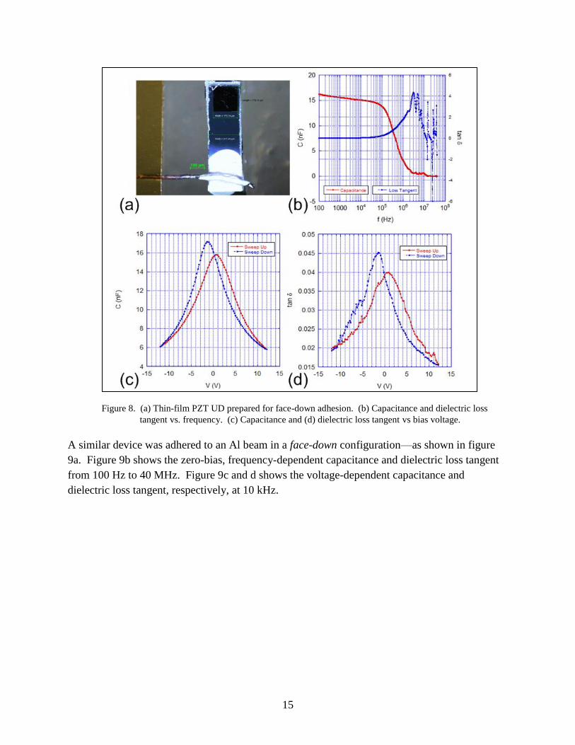
to the Al beams, as shown in figure 8a. Figure 8b displays this devices’s frequency-dependent
capacitance and dielectric loss tangent from 100 Hz to 40 MHz with zero voltage bias. The
increase in loss tangent in the neighborhood of (3 to 5) MHz suggests resonant behavior. As
shown in figure 8c and d, voltage-dependent capacitance and dielectric loss tangent
measurements were performed the thin-film PZT UDs using a Hewlett-Packard 4194A
impedance gain-phase analyzer. These measurements were obtained using a 10-kHz test signal
with an amplitude of 0.05 V root mean square (RMS). Both characterizations featured sweep-
direction-dependent hysteresis—possibly due to a combination of both piezoelectric and
ferroelectric polarization.
15
Figure 8. (a) Thin-film PZT UD prepared for face-down adhesion. (b) Capacitance and dielectric loss
tangent vs. frequency. (c) Capacitance and (d) dielectric loss tangent vs bias voltage.
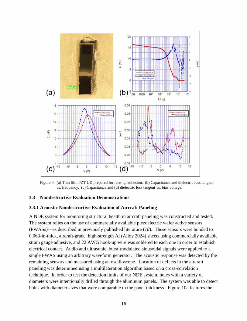
A similar device was adhered to an Al beam in a face-down configuration—as shown in figure
9a. Figure 9b shows the zero-bias, frequency-dependent capacitance and dielectric loss tangent
from 100 Hz to 40 MHz. Figure 9c and d shows the voltage-dependent capacitance and
dielectric loss tangent, respectively, at 10 kHz.
16
Figure 9. (a) Thin film PZT UD prepared for face-up adhesion. (b) Capacitance and dielectric loss tangent
vs. frequency. (c) Capacitance and (d) dielectric loss tangent vs. bias voltage.
3.3 Nondestructive Evaluation Demonstrations
3.3.1 Acoustic Nondestructive Evaluation of Aircraft Paneling
A NDE system for monitoring structural health in aircraft paneling was constructed and tested.
The system relies on the use of commercially available piezoelectric wafer active sensors
(PWASs)—as described in previously published literature (18). These sensors were bonded to
0.063-in-thick, aircraft-grade, high-strength Al (Alloy 2024) sheets using commercially available
strain gauge adhesive, and 22 AWG hook-up wire was soldered to each one in order to establish
electrical contact. Audio and ultrasonic, burst-modulated sinusoidal signals were applied to a
single PWAS using an arbitrary waveform generator. The acoustic response was detected by the
remaining sensors and measured using an oscilloscope. Location of defects in the aircraft
paneling was determined using a multilateration algorithm based on a cross-correlation
technique. In order to test the detection limits of our NDE system, holes with a variety of
diameters were intentionally drilled through the aluminum panels. The system was able to detect
holes with diameter sizes that were comparable to the panel thickness. Figure 10a features the
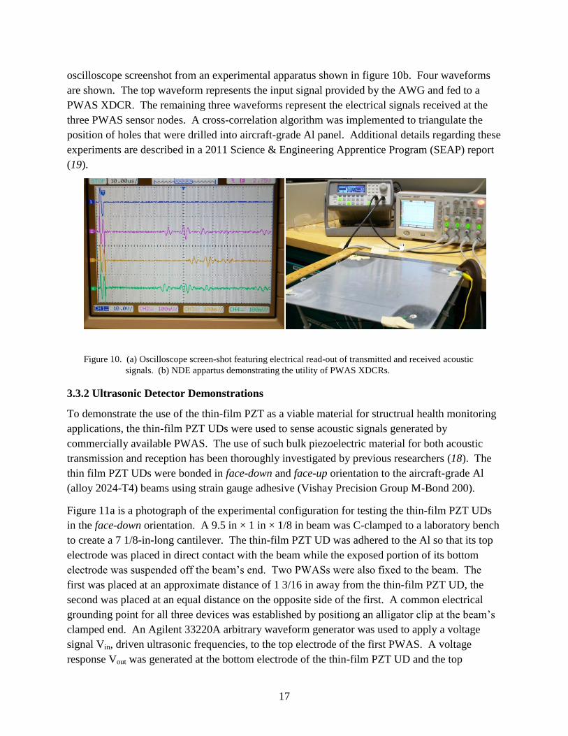
17
oscilloscope screenshot from an experimental apparatus shown in figure 10b. Four waveforms
are shown. The top waveform represents the input signal provided by the AWG and fed to a
PWAS XDCR. The remaining three waveforms represent the electrical signals received at the
three PWAS sensor nodes. A cross-correlation algorithm was implemented to triangulate the
position of holes that were drilled into aircraft-grade Al panel. Additional details regarding these
experiments are described in a 2011 Science & Engineering Apprentice Program (SEAP) report
(19).
Figure 10. (a) Oscilloscope screen-shot featuring electrical read-out of transmitted and received acoustic
signals. (b) NDE appartus demonstrating the utility of PWAS XDCRs.
3.3.2 Ultrasonic Detector Demonstrations
To demonstrate the use of the thin-film PZT as a viable material for structrual health monitoring
applications, the thin-film PZT UDs were used to sense acoustic signals generated by
commercially available PWAS. The use of such bulk piezoelectric material for both acoustic
transmission and reception has been thoroughly investigated by previous researchers (18). The
thin film PZT UDs were bonded in face-down and face-up orientation to the aircraft-grade Al
(alloy 2024-T4) beams using strain gauge adhesive (Vishay Precision Group M-Bond 200).
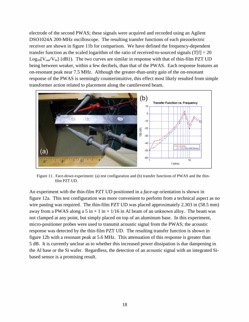
Figure 11a is a photograph of the experimental configuration for testing the thin-film PZT UDs
in the face-down orientation. A 9.5 in × 1 in × 1/8 in beam was C-clamped to a laboratory bench
to create a 7 1/8-in-long cantilever. The thin-film PZT UD was adhered to the Al so that its top
electrode was placed in direct contact with the beam while the exposed portion of its bottom
electrode was suspended off the beam’s end Two PWASs were also fixed to the beam The
first was placed at an approximate distance of 1 3/16 in away from the thin-film PZT UD, the
second was placed at an equal distance on the opposite side of the first. A common electrical
grounding point for all three devices was established by positiong an alligator clip at the beam’s
clamped end. An Agilent 33220A arbitrary waveform generator was used to apply a voltage
signal Vin, driven ultrasonic frequencies, to the top electrode of the first PWAS. A voltage
response Vout was generated at the bottom electrode of the thin-film PZT UD and the top
18
electrode of the second PWAS; these signals were acquired and recorded using an Agilent
DSO1024A 200-MHz oscilloscope. The resulting transfer functions of each piezoelectric
receiver are shown in figure 11b for comparison. We have defined the frequency-dependent
transfer function as the scaled logarithm of the ratio of received-to-sourced signals (T[f] = 20
Log10[Vout/Vin] {dB}). The two curves are similar in response with that of thin-film PZT UD
being between weaker, within a few decibels, than that of the PWAS. Each response features an
on-resonant peak near 7.5 MHz. Although the greater-than-unity gain of the on-resonant
response of the PWAS is seemingly counterintuitive, this effect most likely resulted from simple
transformer action related to placement along the cantilevered beam.
Figure 11. Face-down experiment: (a) test configuration and (b) transfer functions of PWAS and the thin-
film PZT UD.
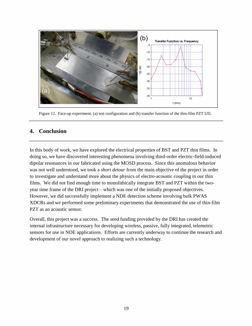
An experiment with the thin-film PZT UD positioned in a face-up orientation is shown in
figure 12a. This test configuration was more convenient to perform from a technical aspect as no
wire pasting was required. The thin-film PZT UD was placed approximately 2.303 in (58.5 mm)
away from a PWAS along a 5 in × 1 in × 1/16 in Al beam of an unknown alloy. The beam was
not clamped at any point, but simply placed on top of an aluminum base. In this experiment,
micro-positioner probes were used to transmit acoustic signal from the PWAS; the acoustic
response was detected by the thin-film PZT UD. The resulting transfer function is shown in
figure 12b with a resonant peak at 5.6 MHz. This attenuation of this response is greater than
5 dB. It is currently unclear as to whether this increased power dissipation is due dampening in
the Al base or the Si wafer. Regardless, the detection of an acoustic signal with an integrated Si-
based sensor is a promising result.
19
Figure 12. Face-up experiment: (a) test configuration and (b) transfer function of the thin-film PZT UD.
4. Conclusion
In this body of work, we have explored the electrical properties of BST and PZT thin films. In
doing so, we have discovered interesting phenomena involving third-order electric-field-induced
dipolar resonances in our fabricated using the MOSD process. Since this anomalous behavior
was not well understood, we took a short detour from the main objective of the project in order
to investigate and understand more about the physics of electro-acoustic coupling in our thin
films. We did not find enough time to monolithically integrate BST and PZT within the two-
year time frame of the DRI project—which was one of the initially proposed objectives.
However, we did successfully implement a NDE detection scheme involving bulk PWAS
XDCRs and we performed some preliminary experiments that demonstrated the use of thin-film
PZT as an acoustic sensor.
Overall, this project was a success. The seed funding provided by the DRI has created the
internal infrastructure necessary for developing wireless, passive, fully integrated, telemetric
sensors for use in NDE applications. Efforts are currently underway to continue the research and
development of our novel approach to realizing such a technology.
20
5. References
1. Toonen, R. C.; Fu, R. X.; Ivill, M. P.; Hirsch, S. G.; Cole, M. W.; Zheleva, T. S. A Fully
Integrated Materials Framework for Enabling the Wireless Detection of Micro-defects in
Aging and Battle-worn Structures; ARL-MR-0775; U.S. Army Research Laboratory:
Aberdeen Proving Ground, MD, April 2011.
2. Morito, K.; Iwazaki, Y.; Suzuki, T.; Fujimoto, M. J. Appl. Phys. 2003, 94, 5199.
3. Gevorgian, S.; Vorobiev, A.; Lewin, T. J. Appl. Phys. 2006, 99, 124112.
4. Tappe, S.; Böttger, U.; Waser, R. Appl. Phys. Lett. 2004, 85, 624.
5. Noeth, A.; Yamada, T.; Sherman, V. O.; Muralt, P.; Tagantsev, A. K.; Setter, N. J. Appl.
Phys. 2007, 102, 114110.
6. Cole, M. W.; Geyer, R. G. Mechanics of Materials 2004, 36, 1017.
7. Cole, M. W.; Toonen, R. C.; Ivill, M.; Hirsch, S. G.; Ngo, E.; Hubbard, C. J. Appl. Phys.
2011, 110, 124105.
8. Nishiyama, H.; Nakamura, M. IEEE Trans. Comp., Hybrids, Manuf. Technol. 1993, 16, 360.
9. Bevington, P. R.; Robinson, D. K. Data Reduction and Error Analysis for the Physical
Sciences, McGraw-Hill, New York, 43–48, 1992.
10. Barker, A. S.; Hopfield, J. J. Phys. Rev. 1964, 135, A1732.
11. von Hippel, A. R. Dielectrics and Waves; Wiley, New York, 1954, pp. 102, 161.
12. Yor B “Tunable dielectrics for RF circuits ” in Multifunctional Adaptive Microwave
Circuits and Systems, M. Steer, Ed. Raleigh, NC:Scitech, 2009.
13. Basceri, C.; Streiffer, S. K.; Kingon, A. I.; Waser, R. J. Appl. Phys. 1997, 82, 2497.
14. Pertsev, N. A;. Zembilgotov, A. G.; Tagantsev, A. K. Phys. Rev. Lett. 1998, 80, 1988.
15. Zhang, J.; Heitmann, A. A.; Alpay, S .P.; Rossetti, G. A., Jr. J. Mater. Sci. 2009, 44, 5263.
16. Chase, D.; Chen, L.-Y.; York, R. IEEE Trans. Microwave Theory Tech. 2005, 53, 3215.
17. Damjanovic, D. Rep. Prog. Phys. 61, 1267, 1998.
18. Giurgiutiu, V.; Zagrai, A. N.; Bao, J. J. Structural Health Monitoring 2002, 1, 41–61.
19. Elburn, E.; Toonen, R. Acoustic Nondestructive Evaluation of Aircraft Paneling Using
Piezoelectric Sensors, in preparation.
21
6. Transitions
This effort has resulted in journal paper, two conference papers, three ARL reports (including
this document), and multiple conference presentations. Fabrication developments and
measurement techniques have been successfully transitioned into the mission and customer
programs of the Integrated Electromagnetic Materials Team.
6.1 Journal Papers
Toonen, Ryan C.; Cole, M. W. Third-Order Electric-Field-Induced Dipolar Resonances from
Patterned Barium-Strontium-Titanate Thin-Films. Submitted to Applied Physics Letters on
February 27, 2012; accepted May 2012.
6.2 Conference Papers
Fu, R. X.; Toonen, R. C.; Ngo, E. H.; Cole, M. W.; Hirsch, S. G.; Ivill, M. P.; Hubbard, C.W.
Pb(Zr,Ti)O3 (PZT) Thin Film Sensors for Fully-Integrated, Passive Telemetric
Transponders. Sensors & Transducers J. 2011, 11, 34.
Toonen, R. C.; Ngo, E. H.; Cole, M. W.; Hirsch, S. G.; Ivill, M. P.; Hubbard, C. W.; Fu, R. X.
Tunable Split-Ring Resonator Devices for Compact, Frequency-Selective, Back-Scatter
Transponders, 27th Army Science Conf. Proc. NP-12, December 2010.
6.3 ARL Reports
Toonen, R. C.; Fu, R. X.; Ivill, M. P.; Hirsch, S. G.; Cole, M. W.; Zheleva, T. S. A Fully
Integrated Materials Framework for Enabling the Wireless Detection of Micro-defects in
Aging and Battle-worn Structures; ARL-MR-0775; U.S. Army Research Laboratory:
Aberdeen Proving Ground, MD, April 2011.
Elburn, E.; Toonen, R. Acoustic Nondestructive Evaluation of Aircraft Paneling Using
Piezoelectric Sensors; in preparation.
6.4 Oral Presentations
Fu, R. X.; Toonen, R. C.; Ivill, M. P.; Hirsch, S. G.; Brown, N.; Cole, M. W. Fully‐Integrated,
Thin‐Film Piezoelectric Sensors for Wireless, Non‐Destructive Evaluation of Aging
Structures, 20th IEEE International Symposium on Applications of Ferroelectrics /
International Symposium on Piezoresponse Force Microscopy & Nanoscale Phenomena in
Polar Materials (ISAF-2011-PFM) Joint Conference, Vancouver, Canada, July 24-27, 2011,.
Brown, N.; Toonen, R. C.; Archibald, W.; Cole, M. W. The Speed of Sound Through PZT.
Twelfth Annual Fall Research Symposium, College of Science & Mathematics, University
of the Virgin Islands, St. Thomas Campus, Fall Semester 2010.
22
6.5 Poster Presentations
Fu, R. X.; Toonen, R. C.; Ivill, M. P.; Ngo, E. H.; Cole, M. W.; Hirsch, S. G.; Hubbard, C. W
Integrated Piezoelectric and Ferroelectric Thin Films for Passive Telemetric Transponders,
20th IEEE International Symposium on Applications of Ferroelectrics / International
Symposium on Piezoresponse Force Microscopy & Nanoscale Phenomena in Polar Materials
(ISAF-2011-PFM) Joint Conference, Vancouver, Canada July 24–27, 2011.
Toonen, R. C.; Ngo, E. H.; Cole, M. W.; Hirsch, S. G.; ; Ivill, M. P.; Hubbard, C. W. A Fully-
Integrated Materials Framework for Enabling the Wireless Detection of Micro-Defects in
Aging and Battle-Worn Structures, 27th Army Science Conference; JW Marriott, November
29 – December 2, 2010, Orlando, FL.
Archibald, W.; Brown, N.; Toonen, R. C.; Cole, M. W. Structural Health Monitoring System for
Military Vehicles and Aircrafts, 2010 Materials Research Society Fall Meeting & Exhibit,
Boston, MA, November 29–December 3, 2010.
23
List of Symbol, Abbreviations, and Acronyms
Al aluminum
Al2O3 sapphire
ARL U.S. Army Research Laboratory
BOE buffered oxide etchant
BaTiO3 barium titanate
BST barium strontium titanate
BW bandwidth
CFA conventional furnace annealing
C-V capacitance-voltage
DAQ data acquisition unit
DoD Department of Defense
DRI Director’s Research Initiative
DSP digital signal processing
DUT device under test
EM electromagnetic
FPGA field-programmable gate array
GWU George Washington University
HF hydrofluoric acid
TEM transmission electron microscope
I In-Phase
IC integrated circuit
IDC inter-digital finger capacitor
ISM industrial, scientific, and medical
LDG Landau-Devonshire-Ginzberg
24
MIM metal-insulator-metal
MOSD metal organic solution deposition
MW microwave
NDE nondestructive evaluation
NH4F ammonium fluoride
NiCr nickel chromium alloy
PM phase modulation
Pt platinum
PWASs piezoelectric wafer active sensors
PZT lead zirconate titanate
Q Quadrature
RBS Rutherford backscattering spectrometry
RFID radio frequency identification
RMS root mean square
RTA rapid thermal annealer
SEAP Science & Engineering Apprentice Program
Si silicon
SOL short-open-load
SrTiO3 strontium titanate
TX/RX transmitting/receiving
UD ultrasonic detector
UV ultraviolet
VCO voltage controlled oscillator
XDCR piezoelectric transducer
25
No. of
Copies Organization
4 HCS US ARMY RSRCH LAB
ATTN RDRL WMM E
R C TOONEN
M P IVILL
S GARY HIRSCH,
M W COLE
BLDG 4600
ABERDEEN PROVING GROUND MD
21005-5066
4 HCS US ARMY RSRCH LAB
ATTN RDRL SEE E R FU
ATTN RDRL SEE G WOOD
ATTN RDRL SEE E K ALIBERTI
ATTN RDRL SED E T ZHELEVA
2800 POWDER MILL ROAD
ADELPHI MD 20783-1197
TOTAL: 8 HCS

26
INTENTIONALLY LEFT BLANK.