a design of swastika shaped wideband microstrip patch...
TRANSCRIPT
Journal of Electromagnetic Analysis and Applications, 2014, 6, 31-37 Published Online February 2014 (http://www.scirp.org/journal/jemaa) http://dx.doi.org/10.4236/jemaa.2014.63005
OPEN ACCESS JEMAA
A Design of Swastika Shaped Wideband Microstrip Patch Antenna for GSM/WLAN Application
Vivek Singh Rathor1, Jai Prakash Saini2
1Mewar University, Chittorgarh, India; 2Department of EC, Bundelkhand Institute of Engineering and Technology, Jhansi, India. Email: [email protected], [email protected] Received November 25th, 2013; revised December 28th, 2013; accepted January 25th, 2014 Copyright © 2014 Vivek Singh Rathor, Jai Prakash Saini. This is an open access article distributed under the Creative Commons At- tribution License, which permits unrestricted use, distribution, and reproduction in any medium, provided the original work is proper- ly cited. In accordance of the Creative Commons Attribution License all Copyrights © 2014 are reserved for SCIRP and the owner of the intellectual property Vivek Singh Rathor, Jai Prakash Saini. All Copyright © 2014 are guarded by law and by SCIRP as a guardian.
ABSTRACT This paper presents a compact microstrip patch antenna at operating frequency of 2.5 GHz. The radiating element of the proposed antenna consists of Swastika symbol patch using dielectric substrate 4.2, loss tangent 0.0012 and having the same substrate height 1.6 mm. The antenna size is very compact (28.8 mm × 37.2 mm × 1.6 mm) and covers 1.696 GHz to 2.646 GHz and can be used for GSM and WLAN applications. Using IE3D software package of Zealand, the designed antenna is simulated. The computer simulation results show that the antenna can realize wideband characteristics having good impedance bandwidth of 43.758% (VSWR ≤ 2) for all resonant frequencies. Our aim is to reduce the size of the antenna as well as increase the impedance band- width. KEYWORDS Microstrip Antenna; Wide Band; Swastika Shape; IE3D
1. Introduction In recent years demand for small antennas on wireless communication has increased the interest of research work on compact microstrip antenna design among mi- crowaves and wireless engineers. To support the high mobility necessity for a wireless telecommunication de- vice, a small and light weight antenna is likely to be pre- ferred. For this purpose compact microstrip antenna is one of the most suitable applications. The development of antenna for wireless communication also requires an antenna with more than one operating frequencies. This is due to many reasons, mainly because there are various wireless communication systems and many telecommu- nication operators using various frequencies [1]. How- ever, the general microstrip patch antennas have some disadvantages such as narrow bandwidth etc. Enhance-ment of the performance to cover the demanding band-width is necessary [2]. Among these standards, the fol-lowing frequency bands can be mentioned: 1) PCS-1900 requires a band of 1.85 - 1.99 GHz; 2) IEEE 802.11b/g requires a band of 2.4 - 2.484 GHz; 3) IEEE 802.11a
requires a band of 5.15 - 5.35 GHz and an additional band of 5.725 - 5.825 GHz; 4) HiperLAN2 requires a band of 5.47 - 5.725 GHz besides the band of 5.15 - 5.35 GHz. Microstrip antennas are very attractive because of their low profile, low weight, conformal to the surface of objects and easy production. A large number of micro- strip patches to be used in wireless applications have been developed; various shapes such as square, rectangle, ring, disc, triangle, elliptic, pentagonal [3]. There are numerous and well-known methods to increase the band- width of antennas, including increase of the substrate thickness, the use of a low dielectric substrate, the use of various impedance matching and feeding techniques, and the use of multiple resonators. So we want an antenna which offers a low profile, wide bandwidth, high gain and compact antenna element [2-22]. To overcome the above problem, a microstrip antenna structure with a typical Swastika symbol shaped slot is proposed which exhibits good impedance bandwidth of 43.758% which is suitable for GSM and WLAN (lower band application). Previously several papers have been published on the
A Design of Swastika Shaped Wideband Microstrip Patch Antenna for GSM/WLAN Application
OPEN ACCESS JEMAA
32
same shape but differ from this paper on design consid- eration, size, design parameters, operating frequency etc. Ram Singh [14] uses slotted patch, a compact triple band slot microstrip patch antenna for 1.7/2.92 GHz WLAN applications. IE3D software is used for simulation work and slotted patch is used, which gives triple band. The radiating element of the proposed antenna consists of Swastika symbol slot operating at 1.8 GHz, 2.09 GHz, and 2.92 GHz bands, while Metamaterial Left-Handed Transmission Line model proposed by Vishav Gaurav Bhartiya [15] was presented. Authors analyze a Swastik design of metamaterial structure with a Rectangular Mi- crostrip Patch Antenna and discussed and analyzed the performance of Patch Antenna with and without using the metamaterial structure. K. Jagadeesh Babu [16] pro- posed two element MIMO system resonates at a triband of 3.3 GHz, 5.8 GHz, and 7.1 GHz with an improved impedance bandwidth of 37%. Modani, Uma Shankar [17] used HFSS and gave the stress on return loss. The proposed antenna has simulated return loss of −29.5 dB at 5.8 GHz frequency. The peak gain of this antenna at resonance frequency is 1.6 dB. Vipul Jain [18] uses CST microwave studio and gives stress on characterization of “Swastik” shape and its effect on frequency domain pa- rameter. Avinish Kumar Tripathi [19] proposed antenna on 1.8 GHz (L-band) and 2.5 GHz (S-band) frequentcy, which gives bandwidth of 18.3% & 23.3% respectively.
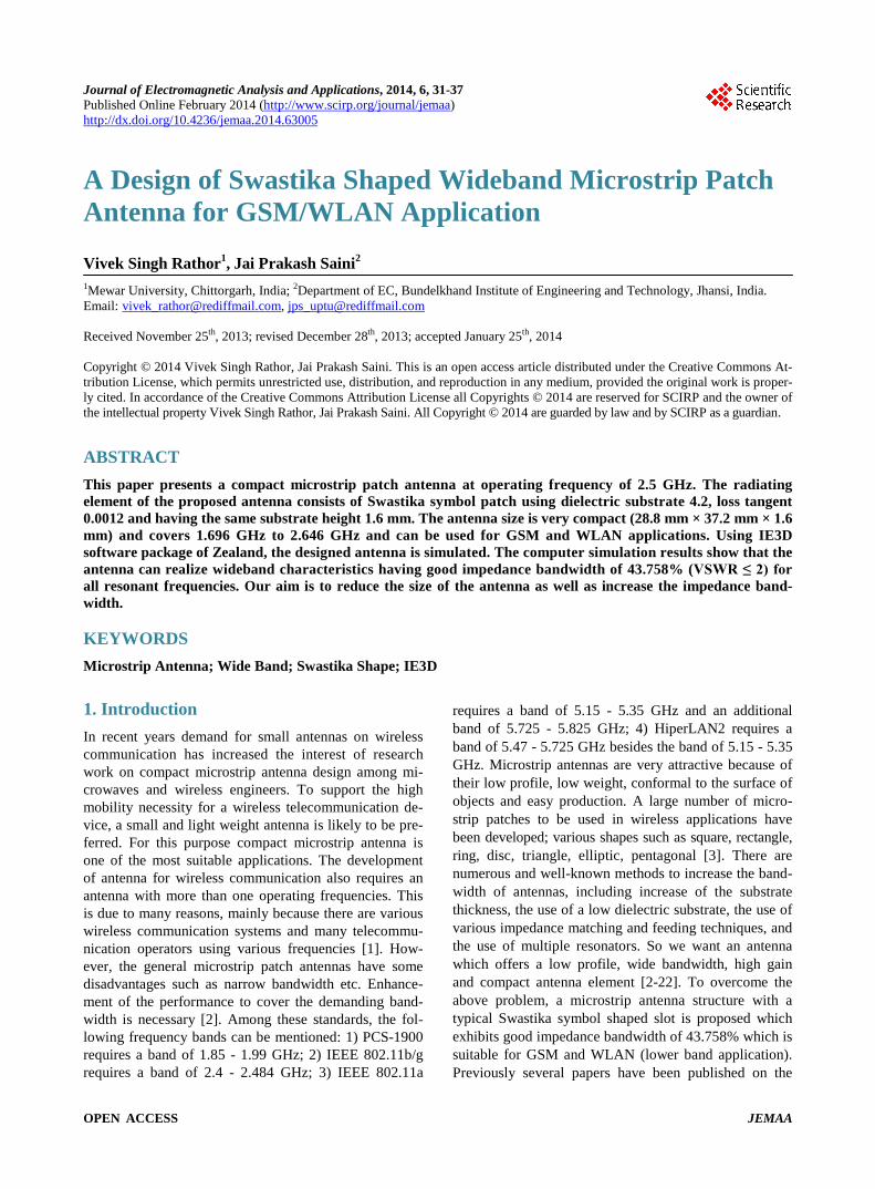
2. Antenna Design The dielectric constant of the substrate is closely related to the size and the bandwidth of the microstrip antenna. Low dielectric constant of the substrate produces larger bandwidth. The resonant frequency of microstrip antenna and the size of the radiation patch can be similar to the following formulas while the high dielectric constant of the substrate results in smaller size of antenna [1]. Fig- ure 1 shows the geometry of the design in which the Length of ground plane of Antenna is 38.4 mm and Width is 46.8 mm, L & W of the patch is 28.8 mm & 37.2 mm.
The patch width, effective dielectric constant, the length extension and also patch length are given by
2 r
cWf ε
= (1)
where c is the velocity of light, rε is the dielectric con- stant of substrate, f is the antenna working frequency, W is the patch non resonant width, and the effective dielec- tric constant is effε given as,
( ) ( )121 1
1 102 2
r reff
HW
ε εε
−+ − = + + (2)
Figure 1. Top view of the microstrip patch antenna.
The extension length ∆ is calculates as,
( )
( )
0.300 0.2620.412
0.258 0.813
eff
eff
WL H
WHH
ε
ε
+ + ∆ = − +
(3)
By using above equation we can find the value of ac- tual length of the patch as,
22 eff
cL Lf ε
= − ∆ (4)
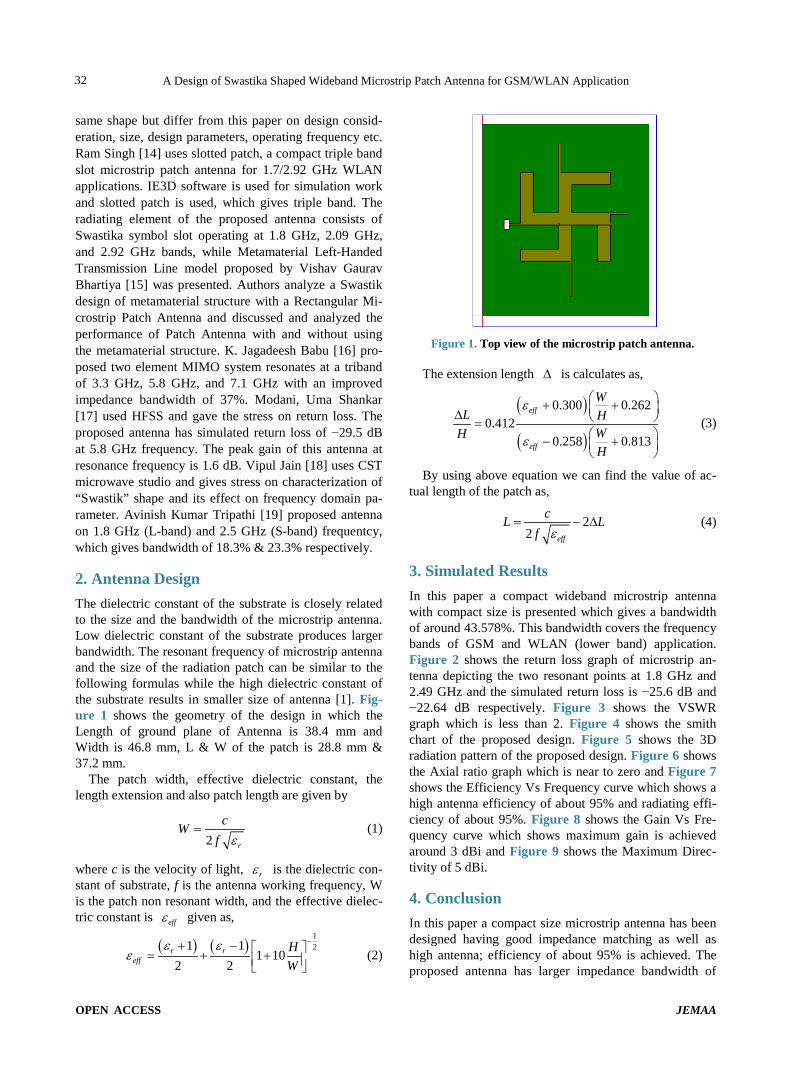
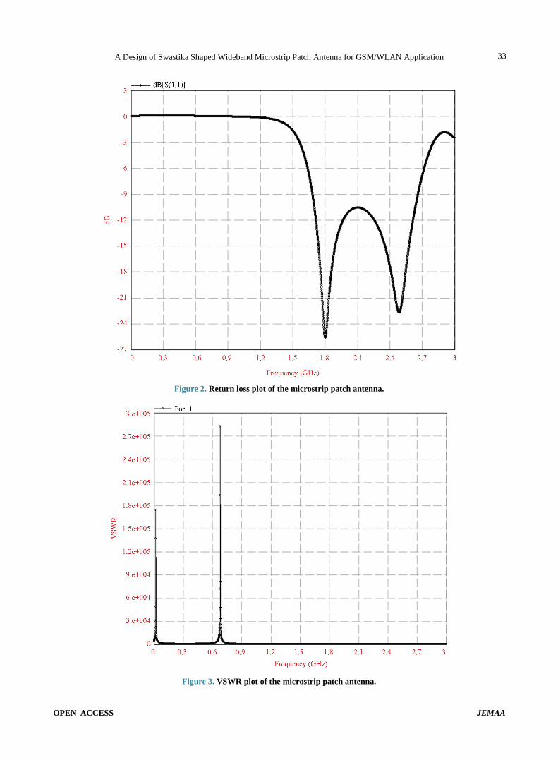
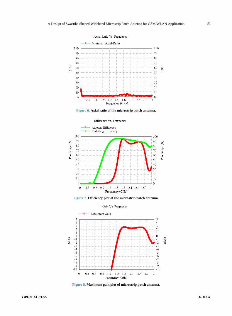
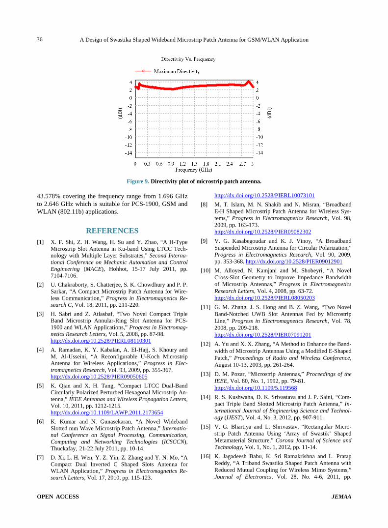
3. Simulated Results In this paper a compact wideband microstrip antenna with compact size is presented which gives a bandwidth of around 43.578%. This bandwidth covers the frequency bands of GSM and WLAN (lower band) application. Figure 2 shows the return loss graph of microstrip an- tenna depicting the two resonant points at 1.8 GHz and 2.49 GHz and the simulated return loss is −25.6 dB and −22.64 dB respectively. Figure 3 shows the VSWR graph which is less than 2. Figure 4 shows the smith chart of the proposed design. Figure 5 shows the 3D radiation pattern of the proposed design. Figure 6 shows the Axial ratio graph which is near to zero and Figure 7 shows the Efficiency Vs Frequency curve which shows a high antenna efficiency of about 95% and radiating effi- ciency of about 95%. Figure 8 shows the Gain Vs Fre- quency curve which shows maximum gain is achieved around 3 dBi and Figure 9 shows the Maximum Direc- tivity of 5 dBi.
4. Conclusion In this paper a compact size microstrip antenna has been designed having good impedance matching as well as high antenna; efficiency of about 95% is achieved. The proposed antenna has larger impedance bandwidth of
A Design of Swastika Shaped Wideband Microstrip Patch Antenna for GSM/WLAN Application
OPEN ACCESS JEMAA
33
Figure 2. Return loss plot of the microstrip patch antenna.
Figure 3. VSWR plot of the microstrip patch antenna.
A Design of Swastika Shaped Wideband Microstrip Patch Antenna for GSM/WLAN Application
OPEN ACCESS JEMAA
34
Figure 4. Smith chart of the microstrip patch antenna.
Figure 5. 3D Radiation pattern plot of the microstrip patch.
A Design of Swastika Shaped Wideband Microstrip Patch Antenna for GSM/WLAN Application
OPEN ACCESS JEMAA
35
Figure 6. Axial ratio of the microstrip patch antenna.
Figure 7. Efficiency plot of the microstrip patch antenna.
Figure 8. Maximum gain plot of microstrip patch antenna.
A Design of Swastika Shaped Wideband Microstrip Patch Antenna for GSM/WLAN Application
OPEN ACCESS JEMAA
36
Figure 9. Directivity plot of microstrip patch antenna.
43.578% covering the frequency range from 1.696 GHz to 2.646 GHz which is suitable for PCS-1900, GSM and WLAN (802.11b) applications.
REFERENCES [1] X. F. Shi, Z. H. Wang, H. Su and Y. Zhao, “A H-Type
Microstrip Slot Antenna in Ku-band Using LTCC Tech- nology with Multiple Layer Substrates,” Second Interna- tional Conference on Mechanic Automation and Control Engineering (MACE), Hohhot, 15-17 July 2011, pp. 7104-7106.
[2] U. Chakraborty, S. Chatterjee, S. K. Chowdhury and P. P. Sarkar, “A Compact Microstrip Patch Antenna for Wire-less Communication,” Progress in Electromagnetics Re-search C, Vol. 18, 2011, pp. 211-220.
[3] H. Sabri and Z. Atlasbaf, “Two Novel Compact Triple Band Microstrip Annular-Ring Slot Antenna for PCS- 1900 and WLAN Applications,” Progress in Electromag- netics Research Letters, Vol. 5, 2008, pp. 87-98. http://dx.doi.org/10.2528/PIERL08110301
[4] A. Ramadan, K. Y. Kabalan, A. El-Hajj, S. Khoury and M. Al-Usseini, “A Reconfigurable U-Koch Microstrip Antenna for Wireless Applications,” Progress in Elec-tromagnetics Research, Vol. 93, 2009, pp. 355-367. http://dx.doi.org/10.2528/PIER09050605
[5] K. Qian and X. H. Tang, “Compact LTCC Dual-Band Circularly Polarized Perturbed Hexagonal Microstrip An-tenna,” IEEE Antennas and Wireless Propagation Letters, Vol. 10, 2011, pp. 1212-1215. http://dx.doi.org/10.1109/LAWP.2011.2173654
[6] K. Kumar and N. Gunasekaran, “A Novel Wideband Slotted mm Wave Microstrip Patch Antenna,” Internatio- nal Conference on Signal Processing, Communication, Computing and Networking Technologies (ICSCCN), Thuckafay, 21-22 July 2011, pp. 10-14.
[7] D. Xi, L. H. Wen, Y. Z. Yin, Z. Zhang and Y. N. Mo, “A Compact Dual Inverted C Shaped Slots Antenna for WLAN Application,” Progress in Electromagnetics Re-search Letters, Vol. 17, 2010, pp. 115-123.
http://dx.doi.org/10.2528/PIERL10073101 [8] M. T. Islam, M. N. Shakib and N. Misran, “Broadband
E-H Shaped Microstrip Patch Antenna for Wireless Sys-tems,” Progress in Electromagnetics Research, Vol. 98, 2009, pp. 163-173. http://dx.doi.org/10.2528/PIER09082302
[9] V. G. Kasabegoudar and K. J. Vinoy, “A Broadband Suspended Microstrip Antenna for Circular Polarization,” Progress in Electromagnetics Research, Vol. 90, 2009, pp. 353-368. http://dx.doi.org/10.2528/PIER09012901
[10] M. Alloyed, N. Kamjani and M. Shobeyri, “A Novel Cross-Slot Geometry to Improve Impedance Bandwidth of Microstrip Antennas,” Progress in Electromagnetics Research Letters, Vol. 4, 2008, pp. 63-72. http://dx.doi.org/10.2528/PIERL08050203
[11] G. M. Zhang, J. S. Hong and B. Z. Wang, “Two Novel Band-Notched UWB Slot Antennas Fed by Microstrip Line,” Progress in Electromagnetics Research, Vol. 78, 2008, pp. 209-218. http://dx.doi.org/10.2528/PIER07091201
[12] A. Yu and X. X. Zhang, “A Method to Enhance the Band- width of Microstrip Antennas Using a Modified E-Shaped Patch,” Proceedings of Radio and Wireless Conference, August 10-13, 2003, pp. 261-264.
[13] D. M. Pozar, “Microstrip Antennas,” Proceedings of the IEEE, Vol. 80, No. 1, 1992, pp. 79-81. http://dx.doi.org/10.1109/5.119568
[14] R. S. Kushwaha, D. K. Srivastava and J. P. Saini, “Com-pact Triple Band Slotted Microstrip Patch Antenna,” In-ternational Journal of Engineering Science and Technol-ogy (IJEST), Vol. 4, No. 3, 2012, pp. 907-911.
[15] V. G. Bhartiya and L. Shrivastav, “Rectangular Micro- strip Patch Antenna Using ‘Array of Swastik’ Shaped Metamaterial Structure,” Corona Journal of Science and Technology, Vol. 1, No. 1, 2012, pp. 11-14.
[16] K. Jagadeesh Babu, K. Sri Ramakrishna and L. Pratap Reddy, “A Triband Swastika Shaped Patch Antenna with Reduced Mutual Coupling for Wireless Mimo Systems,” Journal of Electronics, Vol. 28, No. 4-6, 2011, pp.
A Design of Swastika Shaped Wideband Microstrip Patch Antenna for GSM/WLAN Application
OPEN ACCESS JEMAA
37
483-487. [17] U. S. Modani and S. G. Modani, “Design of a Single
Layer Swastik-Shaped Microstrip Patch Antenna,” Inter- national Journal of Operational Research & Optimiza- tion, Vol. 2, No. 2, 2011, p. 455.
[18] V. Jain and J. K. Singh, “Effect of Swastik Shape Modi- fied Ground Plane on Series Feed Micro Strip Patch An- tenna with 2.6 GHz,” International Journal of Research & Technology, Vol. 1, No. 1, 2011, pp. 11-14.
[19] A. K. Tripathi, S. Srivastava and H. P. Sinha, “Design
and Analysis of Swastik Shape Microstrip Patch Antenna at Glass Epoxy Substrate on L-Band and S-Band,” Inter-national Journal of Engineering and Innovative Tech-nology (IJEIT), Vol. 2, No. 7, 2013, pp. 37-41.
[20] C. A. Balanis, “Antenna Theory,” John Wiley, 1982, pp 727-734.
[21] I. J. Bahl and P. Bharatia, “Microstrip Antennas,” Artech House, 1980.
[22] G. Kumar and K. P. Ray, “Broad Band Microstrip An-tenna,” Artech House, 2003, pp. 1-21.