a current mirror for low voltage, high performance analog circuits
TRANSCRIPT
Analog Integrated Circuits and Signal Processing, 36, 221–233, 2003c© 2003 Kluwer Academic Publishers. Manufactured in The Netherlands.
A Current Mirror for Low Voltage, High Performance Analog Circuits∗
S.S. RAJPUT1 AND S.S. JAMUAR2
1Thin Film Technology Group, National Physical Laboratory, Dr. K.S. Krishnan Marg, New Delhi-110012, India2Department of Electrical and Electronic Engineering, Faculty of Engineering, University Putra Malaysia, Serdang, Malaysia
E-mail: [email protected]
Received November 6, 2001; Revised November 5, 2002; Accepted November 12, 2002
Abstract. A current mirror for low voltage analog and mixed mode circuits is proposed. The current mirror hashigh input and output voltage swing capability and can operate at ±1.0 V supply. P-Spice simulations confirm theinput current range of 1 µA to 500 µA with 2.5 GHz bandwidth for the proposed current mirror. Adaptive biasingincreases the input voltage swing capability and decreases the undesired offset current. Resistive and capacitivecompensation are used to increase its bandwidth.
Key Words: current mirrors, current mode analog signal processing, voltage to current converters
1. Introduction
Recently low power and low voltage analog and mixedmode circuits had gained importance, especially forportable electronics and mobile communication sys-tems. It is predicted that future analog and mixed modecircuits will require power supplies of 1 V or less. Lowpower and thereby low voltage is the ultimate goal so asto reduce the power consumption in peripheral equip-ments which are necessary for instruments cooling.
In all analog and mixed mode VLSI circuits, a cur-rent mirror (CM) is an integral part of a signal pro-cessing elements like op amps, current conveyors, cur-rent feedback amplifiers etc. All high impedance CMtopologies reported so far [1–5] though have high out-put voltage signal swings, but they require a minimuminput voltage (Vin) of at least one threshold voltage(VT ≈ 0.75 V). This voltage is due to the traditionaldiode connected configuration in which input MOS-FET is configured in all the CM structures. There arecertain applications where designer is interested to havelarge input voltage swings even when the CMs em-bedded in the structure are operating at low supplyvoltages. In such applications, CMs with minimum of0.75 V input voltage are unsuitable. This needs inves-tigation into new structures for low voltage (LV) CMs
∗A small part of this paper appeared in APCCAS 2000/IEEE Con-ference Tianjin, China.
having high signal swings both at the input and outputnodes. A few CM topologies with reduced Vin require-ments have already been reported [6, 7]. They use eitherlevel shifter approach or a bulk driven technique [1].But, these CM structures suffer either due to low inputcurrent range (Iin < 150 µA) or smaller bandwidth(<100 MHz) [6, 7].
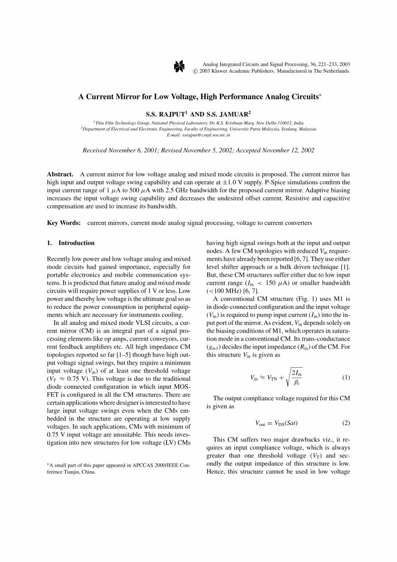
A conventional CM structure (Fig. 1) uses M1 isin diode-connected configuration and the input voltage(Vin) is required to pump input current (Iin) into the in-put port of the mirror. As evident, Vin depends solely onthe biasing conditions of M1, which operates in satura-tion mode in a conventional CM. Its trans-conductance(gm1) decides the input impedance (Rin) of the CM. Forthis structure Vin is given as
Vin ≈ VTN +√
2Iin
βi(1)
The output compliance voltage required for this CMis given as
Vout = VDS(Sat) (2)
This CM suffers two major drawbacks viz., it re-quires an input compliance voltage, which is alwaysgreater than one threshold voltage (VT) and sec-ondly the output impedance of this structure is low.Hence, this structure cannot be used in low voltage
222 Rajput and Jamuar
Fig. 1. Conventional CM structure.
Fig. 2. Conventional cascode mirror.
applications. Also, this structure cannot provide requi-site gains due to its low output impedance. The generalpractice to increase the output impedance of such astructure is to use cascode structure at the output port.Cascode CM of Fig. 2 [8–13] is the example of such anenhanced output impedance CM. However, the inputcompliance voltage of this structure is given as
Vin ≈ 2VTN + 2
√2Iin
βi(3)
which is the double of the input compliance voltageobtained with conventional CM of Fig. 1. Hence, for
Fig. 3. Commonly used low voltage current mirror structure.
Fig. 4. Conventional technique to bias M3 in low voltage currentmirrors.
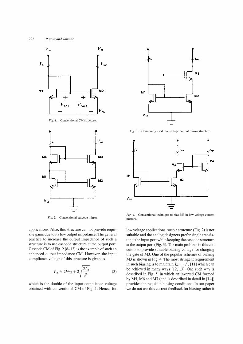
low voltage applications, such a structure (Fig. 2) is notsuitable and the analog designers prefer single transis-tor at the input port while keeping the cascode structureat the output port (Fig. 3). The main problem in this cir-cuit is to provide suitable biasing voltage for chargingthe gate of M3. One of the popular schemes of biasingM3 is shown in Fig. 4. The most stringent requirementin such biasing is to maintain Iref = Iin [11] which canbe achieved in many ways [12, 13]. One such way isdescribed in Fig. 5, in which an inverted CM formedby M5, M6 and M7 (and is described in detail in [14])provides the requisite biasing conditions. In our paperwe do not use this current feedback for biasing rather it
Current Mirror for Low Voltage, High Performance Analog Circuits 223
Fig. 5. A current mirror structure proposed in [14].
Fig. 6. Current mirror proposed in [15].
is used to decrease input compliance voltage and offsetcurrent discussed in detail in following sections.
A CMOS CM proposed by Itakura and Czarnul [15]is shown in Fig. 6. This circuit requires an input volt-age of 86 mV for an input/output current of 100 µA.As the input compliance voltage is quite low, this CMstructure seems to be the most appropriate for low volt-age applications. The voltage across the drain sourceterminals of the mirroring transistors have been main-tained equal and now this is immaterial whether thesetransistors operate in saturation, triode or sub-threshold
regions and the output current will follow the input cur-rent faithfully. However, the transistors, operating insaturation mode, require minimum drain to source volt-age (Veff = VGS − VT). The device parameters and thelevel of input current suggest the mirroring transistorsin the circuit operate in triode region. Any mismatchbetween Ibias1 and Ibias2 will appear as offset current inthe current mirror output. Similarly the mismatch be-tween W5/L5 and W4/L4 will result in different drainto source voltages for mirroring transistors which areoperating in triode region and cause an error in cur-rent gain of the circuit. The frequency response of thisamplifier has not been evaluated in the reference.
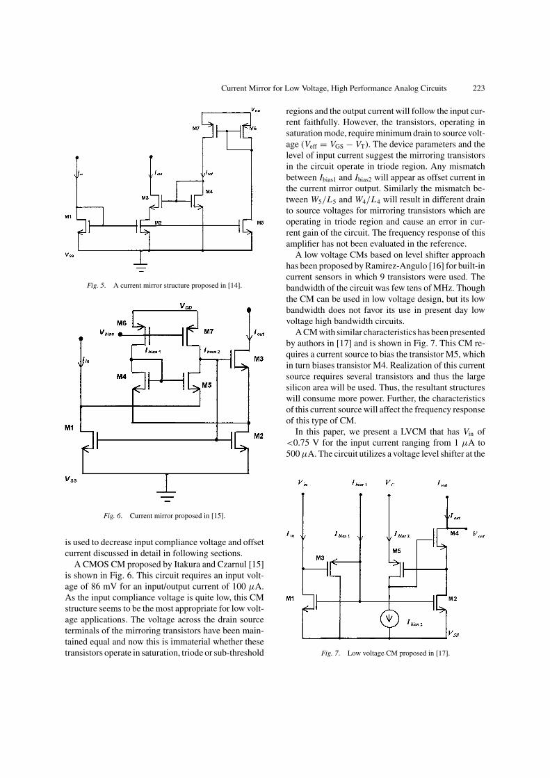
A low voltage CMs based on level shifter approachhas been proposed by Ramirez-Angulo [16] for built-incurrent sensors in which 9 transistors were used. Thebandwidth of the circuit was few tens of MHz. Thoughthe CM can be used in low voltage design, but its lowbandwidth does not favor its use in present day lowvoltage high bandwidth circuits.
A CM with similar characteristics has been presentedby authors in [17] and is shown in Fig. 7. This CM re-quires a current source to bias the transistor M5, whichin turn biases transistor M4. Realization of this currentsource requires several transistors and thus the largesilicon area will be used. Thus, the resultant structureswill consume more power. Further, the characteristicsof this current source will affect the frequency responseof this type of CM.
In this paper, we present a LVCM that has Vin of<0.75 V for the input current ranging from 1 µA to500 µA. The circuit utilizes a voltage level shifter at the
Fig. 7. Low voltage CM proposed in [17].
224 Rajput and Jamuar
input port to achieve the high input voltage swing ca-pability. A resistive compensation has been used to im-prove its bandwidth. A capacitive compensation tech-nique has also been used to improve the bandwidth. Theultimate bandwidth of the proposed LVCM structure is2.5 GHz, and it consumes about 2.0 mW power. Theutilities of this CM in one of the several applicationshave also been demonstrated.
2. Conventional CM Structure
Please refer to Fig. 1, the input voltage (Vin) is givenby Eq. (1). As M1 operates in saturation region, lowerlimit of Vin is restricted to at least VTN. However, Iin canbe too low, which drives M1 into sub-threshold regionand the sub-threshold drain current is given by
ID ≈ W1
L1IDO1 exp
(q(VGS − VTN)
ηkT
)(4)
from which Vin can be calculated as
Vin ≈ ηVtherln
(L1
W1
Iin
IDO1
)+ VTN (5)
where W1 and L1 represent the channel width and chan-nel length for M1. Vther(≈26 mV) is the thermal voltageand η = 1.5. IDO1 is the saturation current and is nor-mally taken as 20 nA [10].
In sub-threshold operation of the circuit (Fig. 1), theinput voltage (Vin) described by Eq. (5) will be suffi-ciently low (≤100 mV), which is one of the most de-sired characteristics of a LVCM. To force M1 and M2into sub-threshold region, one needs to increase the as-pect ratios of these transistors. This lowers the value ofVin. But, the circuits based on sub-threshold MOSFETshave poor frequency response and these circuits cannotbe used in high frequency applications.
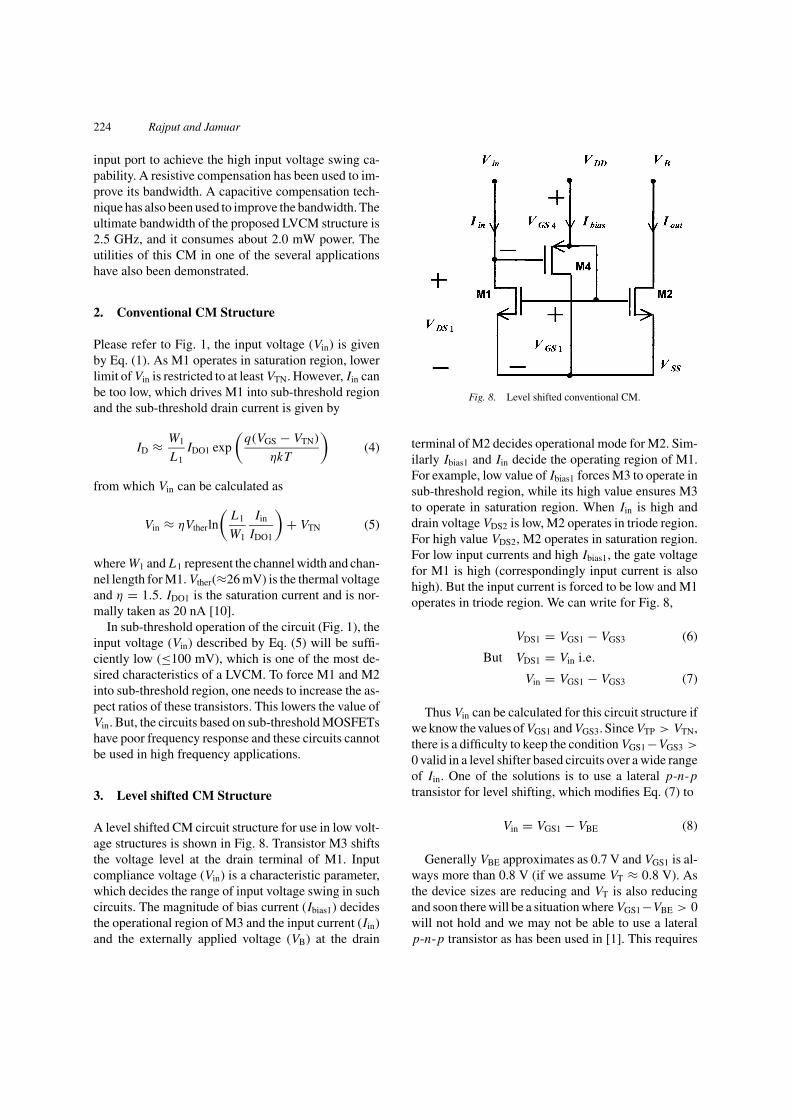
3. Level shifted CM Structure
A level shifted CM circuit structure for use in low volt-age structures is shown in Fig. 8. Transistor M3 shiftsthe voltage level at the drain terminal of M1. Inputcompliance voltage (Vin) is a characteristic parameter,which decides the range of input voltage swing in suchcircuits. The magnitude of bias current (Ibias1) decidesthe operational region of M3 and the input current (Iin)and the externally applied voltage (VB) at the drain
Fig. 8. Level shifted conventional CM.
terminal of M2 decides operational mode for M2. Sim-ilarly Ibias1 and Iin decide the operating region of M1.For example, low value of Ibias1 forces M3 to operate insub-threshold region, while its high value ensures M3to operate in saturation region. When Iin is high anddrain voltage VDS2 is low, M2 operates in triode region.For high value VDS2, M2 operates in saturation region.For low input currents and high Ibias1, the gate voltagefor M1 is high (correspondingly input current is alsohigh). But the input current is forced to be low and M1operates in triode region. We can write for Fig. 8,
VDS1 = VGS1 − VGS3 (6)
But VDS1 = Vin i.e.
Vin = VGS1 − VGS3 (7)
Thus Vin can be calculated for this circuit structure ifwe know the values of VGS1 and VGS3. Since VTP > VTN,there is a difficulty to keep the condition VGS1−VGS3 >
0 valid in a level shifter based circuits over a wide rangeof Iin. One of the solutions is to use a lateral p-n-ptransistor for level shifting, which modifies Eq. (7) to
Vin = VGS1 − VBE (8)
Generally VBE approximates as 0.7 V and VGS1 is al-ways more than 0.8 V (if we assume VT ≈ 0.8 V). Asthe device sizes are reducing and VT is also reducingand soon there will be a situation where VGS1−VBE > 0will not hold and we may not be able to use a lateralp-n-p transistor as has been used in [1]. This requires
Current Mirror for Low Voltage, High Performance Analog Circuits 225
an alternative scheme in place of a p-n-p transistor andthe use of a PMOS transistor will be the most obviousand appropriate choice. Thus, it becomes necessary todiscuss various possible modes of operation this circuitand to identify the suitable modes, which result in thedesirable properties for the resultant LVCM structure.Before, we discuss them we invoke various equations,which describe the drain current of a MOSFET in var-ious regions. Equation (4) describes the operation ofMOSFET is sub-threshold region. The equations de-scribing the operation in other regions are
ID = β
((VGS1 − VTN)VDS − V 2
DS
2
)
(Triode region) (9)
ID = β
2(VGS1 − VTN)2 (Saturation region) (10)
Here all symbols used in above equations have usualmeanings. As discussed, there may be many possiblecombinations in which transistor M1, M2 and M3 canoperate. However, we calculate Vin only for relevantcombinations only.
3.1. M1 and M3 Operating in Sub-ThresholdRegion
When M1 and M3 are in sub-threshold region; the gateto source voltages of M1 and M3 are almost near totheir threshold voltages. The current Ibias1 is given as[18]
Ibias1 ≈ W3
L3IDO3 exp
(VGS3 − VTP
ηVther
)(11)
and VGS3 is given by
VGS3 =∣∣∣∣ηVther ln
{L3
W3
Ibias1
IDO3
}∣∣∣∣ + |VTP| (12)
Similarly, VGS1 is given by
VGS1 = ηVther ln
{L1
W1
Iin
IDO1
}+ VTN (13)
Substituting Eqs. (12) and (13) in Eq. (7), we get
Vin = ηVtherln
{Iin
Ibias1
IDO3
IDO1
L1
L3
W3
W1
}− VT (14)
where
VT = |VTP| − VTN (15)
In this case, we require Iin > Ibias1 and W3 > W1 toensure Vin > 0.
3.2. M1 Operating in Saturation and M3Operating in Sub-Threshold Region
When M1 operates in saturation region, VGS1 is givenas [18]
VGS1 =√
2Iin
β1+ VTN (16)
We get
Vin =√
2Iin
β1− VT − ηVther
∣∣∣∣ ln
(Ibias1
IDO3
L3
W3
)∣∣∣∣ (17)
by using Eqs. (7), (13) and (16).This is the most desirable mode of the operation
of the level shifted CM. The appropriate conditions,which ensure the operation of the level shifted CM inpractical circuits can be set just by appropriate selectionof device parameters (W and L) and input parameters(Iin and Ibias1).
The most suitable operational mode now is opera-tion of M3 in sub-threshold region while M1 operatesin sub-threshold region for low input currents and insaturation region for high input currents. The follow-ing analysis assumes that M3 operates in sub-thresholdregion while M1 can operate in sub-threshold and/orsaturation region. The necessary conditions for theseoperations are
1. The current through M3 should be small enough tokeep M3 in sub-threshold region. CorrespondinglyW/L ratio should also be large. This will increase thedevice capacitance and bandwidth of the resultantstructure will suffer.
2. The current through M1 should be large to keep it insaturation region. However when input current willbe low, M1 will operate in sub-threshold region.
In such a situation only M3 operate in sub-thresholdregion and the mirroring transistors, which decide thefrequency response of the mirror, however, operate in
226 Rajput and Jamuar
saturation region most the time except at low inputcurrents. If these mirroring transistors M1 and M2 arerestricted to operate in saturation region, the lower limitof the currents for these CMs is slightly higher. The fre-quency response of such a CM where mirroring tran-sistors M1 and M2 are in saturation region is high.Since M3 sets the dc operating point, its operation insub-threshold region does not degrades the frequencyresponse. Of course if mirroring transistors operate insub-threshold region, the structure cannot have highbandwidth.
4. Proposed LVCM Structure
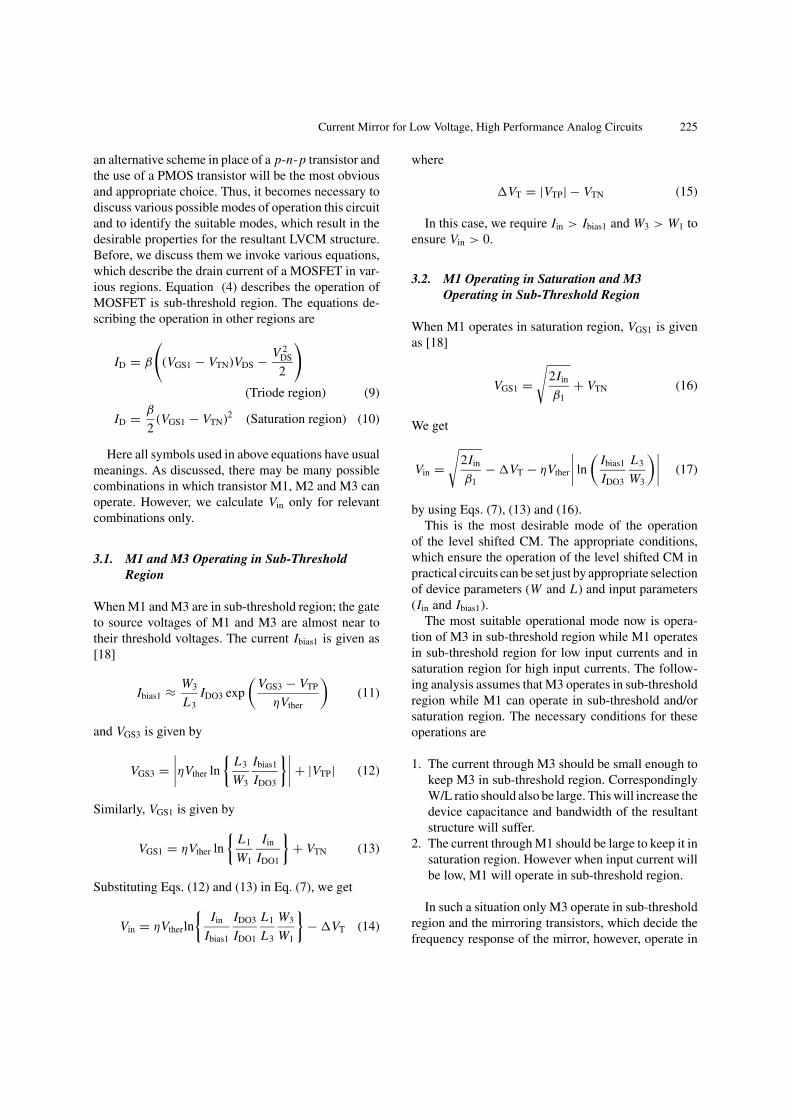
The proposed LVCM is shown in Fig. 9 [18, 19]. Thelevel shifter M3 is forced to operate in sub-thresholdregion by selecting Ibias1 at sufficiently low level.This ensures that Vin always exceeds minimum re-quired voltage (VGS1 − VTN), necessary to drive M1in saturation/sub-threshold region. It is desirable thatM1 and M2 operate either in sub-threshold or in sat-uration region, while M3 should operate only in sub-threshold region. When Iin is zero, M1 will be in sub-threshold region but the operational region of M2 isdecided by the external bias (VB). For low value of VB,M2 will be in triode region while for high VB, M2 willoperate in sub-threshold region.
M5 provides the suitable gate bias to transistor M4.Input current (Iin) injected into M1 is transferred to M2.The use of M4 enhances the output impedance (Rout).
Fig. 9. Proposed level shifted LVCM.
Vin is given by Eq. (16). Input resistance (Rin), outputresistance (Rout) of the proposed LVCM is given as
Rin ≈ 1
gm1(18)
Rout ≈ 1
gd3
(1 + gd4
gd2+ gm4
gm1
gm5
gd5+ gd4
gd2
gm3
gd3
gm2
gd2
)(19)
As the contribution of first three terms of Eq. (19) islower than that of last term, Rout may be approximatedas
Rout ≈ gm3
gd3
gm2
g2d2
(20)
where gd2, gd3, gd4, gd5, gm1, gm2, gm3, gm4, and gm5
have usual meanings.The minimum output voltage necessary for the pro-
posed LVCM is given by
Vout(min) ≈ VDS2(sat) + VDS4(sat) (21)
5. Performance Parameters
LVCM design assumes that all the process parame-ters are ideal, which is never the case [18]. Hence,certain performance indices are required to evaluateits performance. For a current mirror, performance in-dices are input compliance voltage, output compliancevoltage, CM bandwidth, input impedance and outputimpedance etc. Other equally important parametersoriginate due to either the process variations, or arestructural dependent or the environment borne. Theseperformance indices include the offset current, whichis due to the particular circuit architecture and the mis-matches between the various dimensions and processparameters is due the physical process involved. Thesenon-idealities can be minimized but cannot be elimi-nated. The temperature variations a parameter devotedto environmental changes.
5.1. Offset Current
Ioffset is the most disturbing factor in LVCMs that setsthe lower limit of the input current. Due to level shifterM3, the gates of M1 and M2 are not at reference poten-tial even when the input current is zero. Actually, thegate of M2 is at elevated voltage and its drain voltage
Current Mirror for Low Voltage, High Performance Analog Circuits 227
depends on the externally applied voltage (Vds1 is de-cided by Iin). Hence a sub-threshold current will flowin M2 even when Iin equals zero. This current is knownas offset current, which is given as [18]
Ioffset = W2
L2
L3
W3
IDO2
IDO3Ibias1 exp
(VT
ηVther
)(22)
Ioffset can be tailored according to the designers’ needthrough the appropriate selection of W and L . VT de-pends on the selection of particular CMOS technology.Even if the threshold voltages of PMOS and NMOSare matched Ioffset cannot be reduced to zero. The lowerlimit of the Ioffset is given as [18]
Ioffset = W2
L2
L3
W3
IDO2
IDO3Ibias1 (23)
Appropriate selection of W/L ratios for M2 and M3and low value for Ibias1 ensure lower value for Ioffset.
5.2. Sensitivity Analysis
In case of proposed LVCM, sensitivity analysis is usedto ascertain the effects of variations in input parametersand process parameters like Ibias1, threshold voltages,transistor aspect ratios (W/L), and the mismatch be-tween the threshold voltages of PMOS and NMOS,over its performance. The output current (Iout) is givenas
Iout = µCOXW
2L
[Vin +
∣∣∣∣ηVther ln
(L3
W3
Ibias1
IDO3
)∣∣∣∣+ |VTP3| − VTN2
]2
(1 + λVDS2) (24)
The sensitivities of Iout with respect to various param-eters are given as [18]
SIoutVDS2
≈ λVDS2 (25)
SIoutIbias1
≈ W2
L2
W3
L3
2ηVth IDO3 K ′2
gm2(26)
SIoutW ≈ 1 (27)
SIoutL ≈ −1 (28)
SIoutVTN2
≈ −W2
L2
2VTN2 K ′2
gm2(29)
SIoutVTP3
≈ −W2
L2
2VTP3 K ′2
gm2(30)
SIoutVT
≈ −W2
L2
2VT K ′2
gm2(31)
where K ′2 is the trans-conductance parameter (µCOX)
for M2. Here we have used VT = VTP − VTN.The sensitivity analysis shows that the variations in
output current due to the change in input variables arealmost negligible.
5.3. Temperature Effects
Temperature analysis gives the relationship betweenIout and temperature. The mobility (µ) and thresholdvoltage VT are the temperature dependent parameters.Their temperature dependence is given as [8–11, 13]
µ(T ) = µ0T −3/2 (32)
Vt (T ) = Vt (T0) − α(T − T0) (33)
where µ(T0) = 400 cm2 V−1 s−1 and α = 2.3 mV/◦C.The current output from the mirror is given by [18]
Iout = µ(T0)T −3/2 COXW2
2L2
×[
Vin +∣∣∣∣ηkT
qln
(L3
W3
Ibias1
IDO3
)∣∣∣∣ + VT
](34)
Assuming the temperature changes in VT to be neg-ligible (when αn and αp are equal), we get the fractionaltemperature coefficient (TC f ) as [18]
TC f (Iout) ≈ −1.5
T(35)
From the above equation, the TC f (Iout) equals−500 ppm/◦C at room temperature.
6. Adaptively Biased LVCM
If Ibias1 can be reduced, Ioffset reduces proportionately(Eq. (23)). However, an increase in Ibias1 decreases Vin
(Eq. (17)) [17–19]. There is a tradeof between Vin andIoffset, but the reduction in Vin is not too significantwith Ibias1 as it appears in logarithmic term. Thus itis desirable to incorporate engineering compromisesbetween Ioffset and Vin.
228 Rajput and Jamuar
Hence an adaptive biasing is proposed for the pro-posed LVCM in which Ibias1 is reduced to near zeroat low Iin and is increased at high Iin. This facilitatesproposed LVCM to have a minimum Ioffset at low inputcurrents and low Vin at higher Iin.
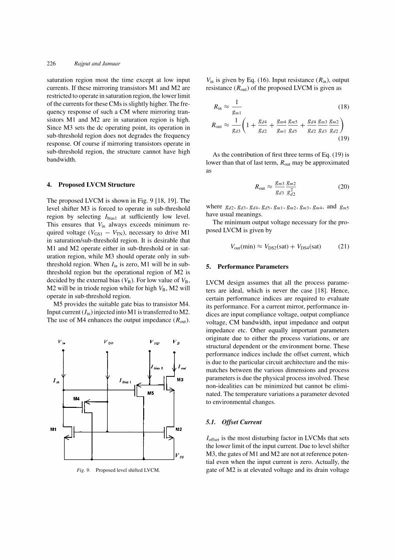
6.1. Circuit Structure
The adaptively biased LVCM is shown in Fig. 10. Thetransistors M6, M7, M8 and M9 have been added toform a CM used for adaptive biasing. A scaled versionof Iin is fed back to M3 as Ibias1, which makes Ibias1
proportional to Iin. So, Ibias1 is low, when Iin is low andhigh when Iin is high. Thus the proposed circuit meetsour requirements as stipulated. Ibias2 for M5 has alsobeen derived from the same mirror structure.
It may be noted that the circuit is stable for zero inputcurrent. However, the circuit does not require a start-up circuit, as the output current is solely dependent onthe input current. The circuit behaves like a currentamplifier and the output is present only when input ispresent and the output is input dependent. Hence, forzero input current output current is zero, which is thestable operating point of the circuit. As the input currentincreases output current follows the input current. Thusthe input current provides the start-up operation for theproposed circuit.
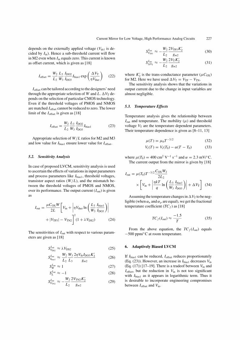
For enhancing the LVCM bandwidth, a resistance(Rg) is used between the gates of M1 and M2 as pro-posed in [20, 21]. The resultant structure is shown
Fig. 10. Proposed adaptively biased LVCM.
Fig. 11. Compensated adaptively biased LVCM.
in Fig. 11. A capacitance is also used in betweenthe drain and gate terminal of M2 for frequencycompensation.
6.2. Existence of Proposed Device Conditions
The proposed ABLVCM structure requires that
(i) Transistor M1 and M2 should operate either in sub-threshold region or saturation region.
(ii) Transistor M3 should operate only in sub-threshold region
The first condition requires that Veff > 0 when M1and M2 are in saturation region. However when M1and M2 are in sub-threshold region, it is ensured withfeeding low current into M1 and M2 and selecting largeW1/L1 = W2/L2. The second condition of having M3into sub-threshold region requires large W3/L3 and lowIbias1. The appropriate selection of these parametersensures that these conditions are met.
6.3. Circuit Response
Refer to the modified and compensated LVCM struc-ture of Fig. 11. Routine circuit analysis carried out forthe structure yields the current transfer function as [18]
Io(s)
Iin(s)≈ gm1gm5
2gd1gd2
1 + sCxgl(
1 + sCingd1
)(1 + sCx
gl
) + gm1gm4
gd1gl
(36)

Current Mirror for Low Voltage, High Performance Analog Circuits 229
where
gl ≈ g + gCgs1
Cgd1+ gd2 (37)
Cx ≈ Cgs1 + Cgs2 + Cgs4 + Cgd1 + Cex (38)
Cin ≈ Cgd4 + Cgd5 + Cgs1 + Cgd1 − Cexgd4
gm4(39)
Cgs1 = Gate to source capacitance of M1Cgd1 = Gate to drain capacitance of M1Cgs2 = Gate to source capacitance of M2Cgs4 = Gate to source capacitance of M4Cgd4 = Gate to drain capacitance of M4Cgd5 = Gate to drain capacitance of M5
g = 1/Rg (40)
For sufficiently high value of gl , Eq. (36) can beapproximated as [18]
Io(s)
Iin(s)≈ gm1gm5
2gd1gd2
1
1 + sCingd1
(41)
Rg shifts the location of zero to coincide with lo-cation of pole. This cancels out the pole with zero inthe transfer function giving an improvement in the fre-quency response.
6.4. Compensation Techniques
Rg enhances the frequency response [20, 21]. Compari-son of Eq. (36) with the standard second order equationyields the damping factor ξ , as [18]
ξ =0.5
√Cingl
gd1Cx+
√gd1Cx
gl Cin√1 + gm1gm3CinCx
g2d1g2
l
(42)
Initially, when Rg = 0 �, gl =∝ (Eqs. (37) and(41)), ξ has near infinite value causing the system tooperate in over damped mode. Decrease in gl due theincrease in gate resistance Rg forces ξ to move to-wards 1 from infinity causing the system to step towardscritically damped region and the bandwidth improves.When gl further decreases as a result of an increasein Rg, system moves away from critically dampedmode towards under damped region and results in thepeaks of overshoots in frequency response. The valueof gl for maximum bandwidth without peaking is given
Table 1. W/L for various transistors.
Current mirrorMOSFETs Type shown in figures W/L (µm/µm)
M1, M2 NMOS 1, 2, 3, 4 48/1.6M3 PMOS 3, 4 48/0.8M4 NMOS 2, 3, 4 12/0.8M5 PMOS 3, 4 12/0.8M6 NMOS 4 4.8/1.6M7, M8 PMOS 4 48/0.8M9 PMOS 4 0.8/16
as [18]
gl = 2Cx gd1
Cin(43)
When an external capacitance (Cex) is used (Fig. 10),effective input capacitance (Cin) decreases (Eq. (39)).This decrease in Cin enhances the bandwidth.
7. Simulation Results
The proposed circuits (Figs. 9 and 11) were simulatedfor 0.8 µm technology with level 3 parameters. The as-pect ratios of different transistors are given in Table 1.For LVCM structure of Fig. 9, Ibias1 and Ibias2 are as-sumed to be 100 pA and 10 µA respectively. Selectioncriterion for Ibias1 is to ensure lower Vin and Ioffset. Ibias2
is selected to ensure the ON condition for M5. All thecircuit operations were simulated for the supply volt-age ±1.0 V. It has been observed that this circuit wascapable of operating at single 1.0 V supply (equiva-lently ±0.5 V). The small signal input impedance forthe circuit was found to be 650 �. The small signaloutput impedance, which is a function of Iout is around3.0 M � when Iin equals 100 µA and reduces to 850 k�
when Iin increases to 500 µA. The structure consumes2.0 mW power.
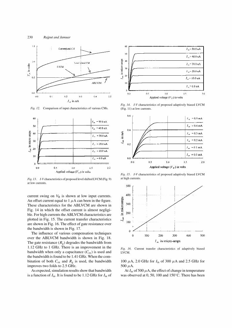
The Vin versus Iin characteristics is shown in Fig. 12in which the comparison between various structures isshown. Clearly, the requirement of the input voltageis lowest in case of adaptively biased LVCM than anyother structure. A reduction of 0.8 V in input voltageis achieved in the input compliance voltage of LVCMand 1.0 V (≈VTP) in the input compliance voltage ofABLVCM.
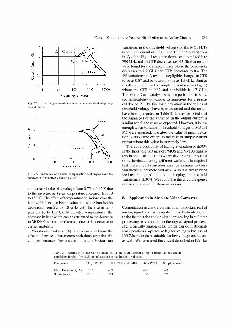
The output current to applied drain bias characteris-tics of M4, (VB) is shown in Fig. 13 for the proposedLVCM of Fig. 11 in which the dependency of output
230 Rajput and Jamuar
Fig. 12. Comparison of input characteristics of various CMs.
Fig. 13. I-V characteristics of proposed level shifted LVCM (Fig. 9)at low currents.
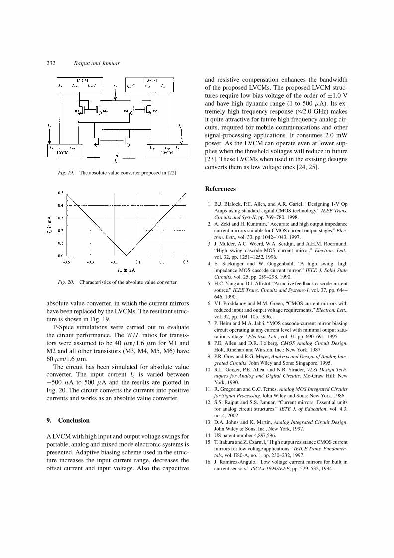
current swing on VB is shown at low input currents.An offset current equal to 1 µA can been in the figure.These characteristics for the ABLVCM are shown inFig. 14 in which the offset current is almost negligi-ble. For high currents the ABLVCM characteristics areplotted in Fig. 15. The current transfer characteristicsare shown in Fig. 16. The effect of gate resistance overthe bandwidth is shown in Fig. 17.
The influence of various compensation techniquesover the ABLVCM bandwidth is shown in Fig. 18.The gate resistance (Rg) degrades the bandwidth from1.12 GHz to 1 GHz. There is an improvement in thebandwidth when only a capacitance (Cex) is used andthe bandwidth is found to be 1.41 GHz. When the com-bination of both Cex and Rg is used, the bandwidthimproves two folds to 2.5 GHz.
As expected, simulation results show that bandwidthis a function of Iin. It is found to be 1.12 GHz for Iin of
Fig. 14. I-V characteristics of proposed adaptively biased LVCM(Fig. 11) at low currents.
Fig. 15. I-V characteristics of proposed adaptively biased LVCMat high currents.
Fig. 16. Current transfer characteristics of adaptively biasedLVCM.
100 µA, 2.0 GHz for Iin of 300 µA and 2.5 GHz for500 µA.
At Iin of 500 µA, the effect of change in temperaturewas observed at 0, 50, 100 and 150◦C. There has been
Current Mirror for Low Voltage, High Performance Analog Circuits 231
Fig. 17. Effect of gate resistance over the bandwidth of adaptivelybiased LVCM.
Fig. 18. Influence of various compensation techniques over thebandwidth of adaptively biased LVCM.
an increase in the bias voltage from 0.75 to 0.95 V dueto the increase in VT as temperature increases from 0to 150◦C. The effect of temperature variations over thebandwidth has also been evaluated and the bandwidthdecreases from 2.5 to 1.8 GHz with the rise in tem-perature (0 to 150◦C). At elevated temperatures, thedecrease in bandwidth can be attributed to the decreasein MOSFETs trans-conductance due to the decrease incarrier mobility.
Worst-case analysis [16] is necessary to know theeffects of process parameters variations over the cir-cuit performance. We assumed 1 and 5% Gaussian
Table 2. Results of Monte Carlo simulation for the circuit shown in Fig. 4 under various circuitconditions for the 10% deviation (Gaussian) in the threshold voltages.
Parameters Only NMOS Both NMOS and PMOS Only PMOS Simple mirror
Mean Deviation (µA) 36.5 −37 −33 −2Sigma (µA) 150 171 35 167
variations in the threshold voltages of the MOSFETsused in the circuit of Figs. 1 and 10. For 5% variationsin VT of the Fig. 11 results in decrease of bandwidth to790 MHz and the CTR decreases to 0.43. Similar resultswere found for the simple mirror where the bandwidthdecreases to 1.2 GHz and CTR decreases to 0.4. The1% variations in VT result in negligible changes in CTRto be as 0.87 and bandwidth to be as 1.5 GHz. Similarresults are there for the simple current mirror (Fig. 1)where the CTR is 0.87 and bandwidth is 1.7 GHz.The Monte-Carlo analysis was also performed to showthe applicability of various assumptions for a practi-cal device. A 10% Gaussian deviation in the values ofthreshold voltages have been assumed and the resultshave been presented in Table 2. It may be noted thatthe sigma (σ ) of the variation in the output current issimilar for all the cases as expected. However, it is lowenough when variation in threshold voltages of M3 andM5 were assumed. The absolute value of mean devia-tion is also same except in the case of simple currentmirror where this value is extremely low.
There is a possibility of having a variation of ±30%in the threshold voltages of PMOS and NMOS transis-tors in practical situations where device structures needto be fabricated using different wafers. It is requiredthat these circuit structures must be immune to thesevariations in threshold voltages. With this aim in mindwe have simulated the circuits keeping the thresholdvariations at ±30%. We found that the circuit responseremains unaltered for these variations.
8. Application in Absolute Value Converter
Computation in analog domain is an important part ofanalog signal processing applications. Particularly, dueto the fact that the analog signal processing is real timeprocessing as compared to the digital signal process-ing. Generally analog cells, which can do mathemat-ical operations, operate at higher voltages but use ofLVCMs make them suitable for low voltage operationsas well. We have used the circuit described in [22] for
232 Rajput and Jamuar
Fig. 19. The absolute value converter proposed in [22].
Fig. 20. Characteristics of the absolute value converter.
absolute value converter, in which the current mirrorshave been replaced by the LVCMs. The resultant struc-ture is shown in Fig. 19.
P-Spice simulations were carried out to evaluatethe circuit performance. The W/L ratios for transis-tors were assumed to be 40 µm/1.6 µm for M1 andM2 and all other transistors (M3, M4, M5, M6) have60 µm/1.6 µm.
The circuit has been simulated for absolute valueconverter. The input current Ic is varied between−500 µA to 500 µA and the results are plotted inFig. 20. The circuit converts the currents into positivecurrents and works as an absolute value converter.
9. Conclusion
A LVCM with high input and output voltage swings forportable, analog and mixed mode electronic systems ispresented. Adaptive biasing scheme used in the struc-ture increases the input current range, decreases theoffset current and input voltage. Also the capacitive
and resistive compensation enhances the bandwidthof the proposed LVCMs. The proposed LVCM struc-tures require low bias voltage of the order of ±1.0 Vand have high dynamic range (1 to 500 µA). Its ex-tremely high frequency response (≈2.0 GHz) makesit quite attractive for future high frequency analog cir-cuits, required for mobile communications and othersignal-processing applications. It consumes 2.0 mWpower. As the LVCM can operate even at lower sup-plies when the threshold voltages will reduce in future[23]. These LVCMs when used in the existing designsconverts them as low voltage ones [24, 25].
References
1. B.J. Blalock, P.E. Allen, and A.R. Gariel, “Designing 1-V OpAmps using standard digital CMOS technology.” IEEE Trans.Circuits and Syst-II, pp. 769–780, 1998.
2. A. Zeki and H. Kuntman, “Accurate and high output impedancecurrent mirrors suitable for CMOS current output stages.” Elec-tron. Lett., vol. 33, pp. 1042–1043, 1997.
3. J. Mulder, A.C. Woerd, W.A. Serdijn, and A.H.M. Roermund,“High swing cascode MOS current mirror.” Electron. Lett.,vol. 32, pp. 1251–1252, 1996.
4. E. Sackinger and W. Guggenbuhl, “A high swing, highimpedance MOS cascode current mirror.” IEEE J. Solid StateCircuits, vol. 25, pp. 289–298, 1990.
5. H.C. Yang and D.J. Allistot, “An active feedback cascode currentsource.” IEEE Trans. Circuits and Systems-I, vol. 37, pp. 644–646, 1990.
6. V.I. Proddanov and M.M. Green, “CMOS current mirrors withreduced input and output voltage requirements.” Electron. Lett.,vol. 32, pp. 104–105, 1996.
7. P. Heim and M.A. Jabri, “MOS cascode-current mirror biasingcircuit operating at any current level with minimal output satu-ration voltage.” Electron. Lett., vol. 31, pp. 690–691, 1995.
8. P.E. Allen and D.R. Holberg, CMOS Analog Circuit Design,Holt, Rinehart and Winston, Inc.: New York, 1987.
9. P.R. Grey and R.G. Meyer, Analysis and Design of Analog Inte-grated Circuits. John Wiley and Sons: Singapore, 1995.
10. R.L. Geiger, P.E. Allen, and N.R. Strader, VLSI Design Tech-niques for Analog and Digital Circuits. Mc-Graw Hill: NewYork, 1990.
11. R. Gregorian and G.C. Temes, Analog MOS Integrated Circuitsfor Signal Processing. John Wiley and Sons: New York, 1986.
12. S.S. Rajput and S.S. Jamuar, “Current mirrors: Essential unitsfor analog circuit structures.” IETE J. of Education, vol. 4.3,no. 4, 2002.
13. D.A. Johns and K. Martin, Analog Integrated Circuit Design.John Wiley & Sons, Inc., New York, 1997.
14. US patent number 4,897,596.15. T. Itakura and Z. Czarnul, “High output resistance CMOS current
mirrors for low voltage applications.” IEICE Trans. Fundamen-tals, vol. E80-A, no. 1, pp. 230–232, 1997.
16. J. Ramirez-Angulo, “Low voltage current mirrors for built incurrent sensors.” ISCAS-1994/IEEE, pp. 529–532, 1994.

Current Mirror for Low Voltage, High Performance Analog Circuits 233
17. S.S. Rajput and S.S. Jamuar, “Low voltage, low power highperformance current mirror for portable analogue and mixedmode applications.” In Proc. IEE—Circuits Devices and Syst,2001, vol. 148, no. 5 pp. 273–278.
18. S.S. Rajput, “Low voltage current mode circuit structures andtheir applications.” Ph.D. Thesis, Indian Institute of Technology,Delhi, 2002.
19. S.S. Rajput and S.S. Jamuar, “A high performance current mirrorfor low voltage designs.” In Proc. APCCAS-2000/IEEE, Tianjin,Dec. 2000, pp. 170–173, China.
20. T. Voo and C. Toumazau, “High speed current mirror resistivecompensation technique.” Electron. Lett., vol. 31, pp. 248–250,1995.
21. T. Voo and C. Toumazau, “Precision temperature stabilized tun-
able CMOS current mirror for filter applications.” Electron. Lett.,vol. 32, pp. 105–106, 1996.
22. I. Baturone, J.L. Huertas, A. Barriga, and S. Sanchez-Solano,“Extending the functionality of a flexible current mode CMOScircuit.” Electron. Lett., vol. 31, no. 15, pp. 1231–1232, 1995.
23. R. Gonzalez, B.M. Gordon, and M.A. Horowitz, “Supply andthreshold voltage scaling for low power CMOS.” IEEE J. SolidState Circuits, vol. 32, no. 8, pp. 1210–1216, 1997.
24. S.S. Rajput and S.S. Jamuar, “Low voltage, low power, highperformance current conveyors.” In ISCAS-2001/IEEE, Sydney,Australia, May 2001, pp. I-723–I-726.
25. S.S. Jamuar and S.S. Rajput, “Low voltage high performanceCCII for analog signal processing applications.” ISIC-2001,Singapore, September 2001 (Invited Talk).