a compact ultrabroadband polarization beam splitter...
TRANSCRIPT
1943-0655 (c) 2016 IEEE. Translations and content mining are permitted for academic research only. Personal use is also permitted, but republication/redistribution requires IEEE permission. Seehttp://www.ieee.org/publications_standards/publications/rights/index.html for more information.
This article has been accepted for publication in a future issue of this journal, but has not been fully edited. Content may change prior to final publication. Citation information: DOI 10.1109/JPHOT.2016.2585113, IEEEPhotonics Journal
A compact ultrabroadband polarization beam splitter utilizing a hybrid plasmonic Y-branch
Ting Hu1, Haodong Qiu1, Zecen Zhang1, Xin Guo1, Chongyang Liu2, Mohamed S. Rouifed 1,
Callum G. Littlejohns1, Graham. T. Reed3, Hong Wang1
1School of Electrical and Electronic Engineering, Nanyang Technological University, 50 Nanyang Avenue, 639798,
Singapore 2Temasek Laboratories, Nanyang Technological University, 50 Nanyang Avenue, 639798, Singapore
3Optoelectronics Research Centre, Building 53, University of Southampton, Southampton, SO17 1BJ, UK
This research is supported by National Research Foundation of Singapore under grant of NRF-CRP12-2013-04 and NTU-A*Star Silicon Technologies Centre of Excellence. Reed is a Royal Society Wolfson Research Merit Award holder and thanks the Wolfson Foundation and the Royal Society for funding the award. Corresponding author: Hong Wang (e-mail: [email protected]).
Abstract: A compact and ultrabroadband polarization beam splitter (PBS) utilizing a hybrid plasmonic Y-branch (HPYB) on silicon-on-insulator platform is proposed and numerically demonstrated. The HPYB consists of a vertical hybrid plasmonic waveguide (HPW) and a horizontal HPW formed by silicon (Si) and silver (Ag) strip waveguides sandwiched with silicon dioxide (SiO2) layer, in which the vertical and horizontal hybrid plasmonic modes (HPMs) are excited by the input transverse-electric (TE) and transverse-magnetic (TM) modes, respectively. The HPMs are split to different ports and coupled back to TE and TM modes to implement the polarization splitting function. A simplified and compact HPYB is robust for the HPMs generation. The structure is wavelength insensitive since the HPMs excitation is weakly correlated to the optical wavelengths. The simulation results show that the HPYB based PBS has a compact footprint of 5 × 1.8 μm2 and an ultra-large working bandwidth of 285 nm, with the polarization crosstalk < -10 dB and the worst case TE (TM) mode insertion loss of -1.53 (-2.35) dB. The device also exhibits large fabrication tolerance of 210 nm variation (from -100 to 110 nm) to the waveguide width for both polarizations.
Index Terms: Integrated optics devices, polarization-selective devices, plasmonics.
1. Introduction
Silicon-on-insulator (SOI) is an attractive platform to implement high-density, cost-effective and energy-saving integration
photonic circuits. The feature of high refractive index contrast between silicon (Si) and silicon dioxide (SiO2) brings the
advantage of making Si photonic device compact. However, this leads to strong birefringence and results in polarization
sensitive problems in sub-micron Si photonic components so that the control and management of polarizations in silicon
photonics is becoming important [1]. The polarization beam splitter (PBS), which has the function of splitting
transverse-electric (TE) and transverse-magnetic (TM) polarization beams to different optical paths, is a key component for
polarization manipulation. A lot of work on PBSs built by all-dielectric waveguides has been reported. The Mach–Zehnder
interferometers (MZIs) based PBS demonstrated in [2] has a length of 200 μm, which is unfavorable for the high density
integration of photonic circuits due to the large footprint. The Bragg grating-assisted couplers based PBSs [3-5], with the
device length of tens micrometers, usually have a working bandwidth below 50 nm due to the limited optical filter bandwidth.
The directional couplers [6, 7] and multimode interferometers (MMIs) [8, 9] based PBSs have the compact footprint with
length and width around or less than 10 μm. For these two types of PBSs, the former ones have larger bandwidth with the
same extinction ratio (ER). However, the bandwidth with 10 dB ER of the PBS proposed in [6] is below 200 nm. Recently, B.
Shen et al. experimentally demonstrated a PBS based on free-form metamaterials [10]. The device has an ultra-compact
footprint of 2.4 × 2.4 μm2, but the bandwidth with 10 dB ER is only 32 nm. Because of the large birefringence of metals,
surface plasmon polarizations (SPPs) can be excited by light with specific polarizations, which provide alternative solutions
for the PBS design. S. Kim et al. transformed the two dimensional SPPs based PBS [11] to a three dimensional structure
and improved the device performance [12]. The device can work within a bandwidth of 280 nm, with the insertion loss (IL) <
-3 dB and ER > 15 dB. However, the device has a vertical taper in the output waveguide, which is a challenge to the
fabrication process. A hybrid plasmonic waveguide (HPW) with a dielectric cylinder above a metal surface has been
reported to take place of SPPs for realizing long propagation distance with lower propagation loss [13], but the cylinder
structure is difficult to fabricate by the planar lightwave circuit technology. Based on this concept, D. Dai et al. proposed the
rectangular metal-SiO2-Si HPW on SOI platform, which reduces the propagation loss and increases the propagation
distance to be on the order of 100 μm [14]. In their following work, the silver (Ag)-SiO2-Si based directional coupler (DC) was
proposed to realize the PBS [15].
In this paper, we propose a PBS by using a hybrid plasmonic Y-branch (HPYB) on the SOI platform. For the PBSs
reported in [11-12], the SPPs serve as the assisted medium to couple TE (TM) mode to the cross output, while in our
proposed PBS, the vertical and horizontal hybrid modes are excited by the input TE and TM modes directly and then split to
different ports, which contributes to the simplified structure and ultra-large working bandwidth of the device. Another
advantage is that it is unnecessary to satisfy the phase-matching condition that is required in the HPW DC based PBS [15,
16]. A compact footprint of 5 × 1.8 μm2 and an ultra-broad bandwidth of 285 nm from 1.861 to 2.146 μm within a crosstalk
(CT) < -10 dB (an equivalent ER > 10 dB) and an IL < -2.35 dB are demonstrated for the proposed PBS by numerical
1943-0655 (c) 2016 IEEE. Translations and content mining are permitted for academic research only. Personal use is also permitted, but republication/redistribution requires IEEE permission. Seehttp://www.ieee.org/publications_standards/publications/rights/index.html for more information.
This article has been accepted for publication in a future issue of this journal, but has not been fully edited. Content may change prior to final publication. Citation information: DOI 10.1109/JPHOT.2016.2585113, IEEEPhotonics Journal
simulations. It has a larger bandwidth than those reported in [2-6, 10-12, 16] and its footprint is comparable to the most
compact PBSs [6-12, 15, 16], with the trade-off of a slightly higher IL. The SPPs based PBS in [12] has a proximate
bandwidth to our proposed device with a better ER, but its IL is higher and the fabrication of its vertical taper is a challenging
job. Further analysis reveals that the proposed PBS has large fabrication tolerance, which allows waveguide width variation
up to 210 nm. Moreover, the working spectral range covers the mid-infrared wavelength of 2 µm, leading to potential
applications in the sensing systems for gas detection, such as carbon dioxide (CO2) and ammonia (NH3) which have large
absorption around this wavelength [17, 18].
2. Principle and Device Designs
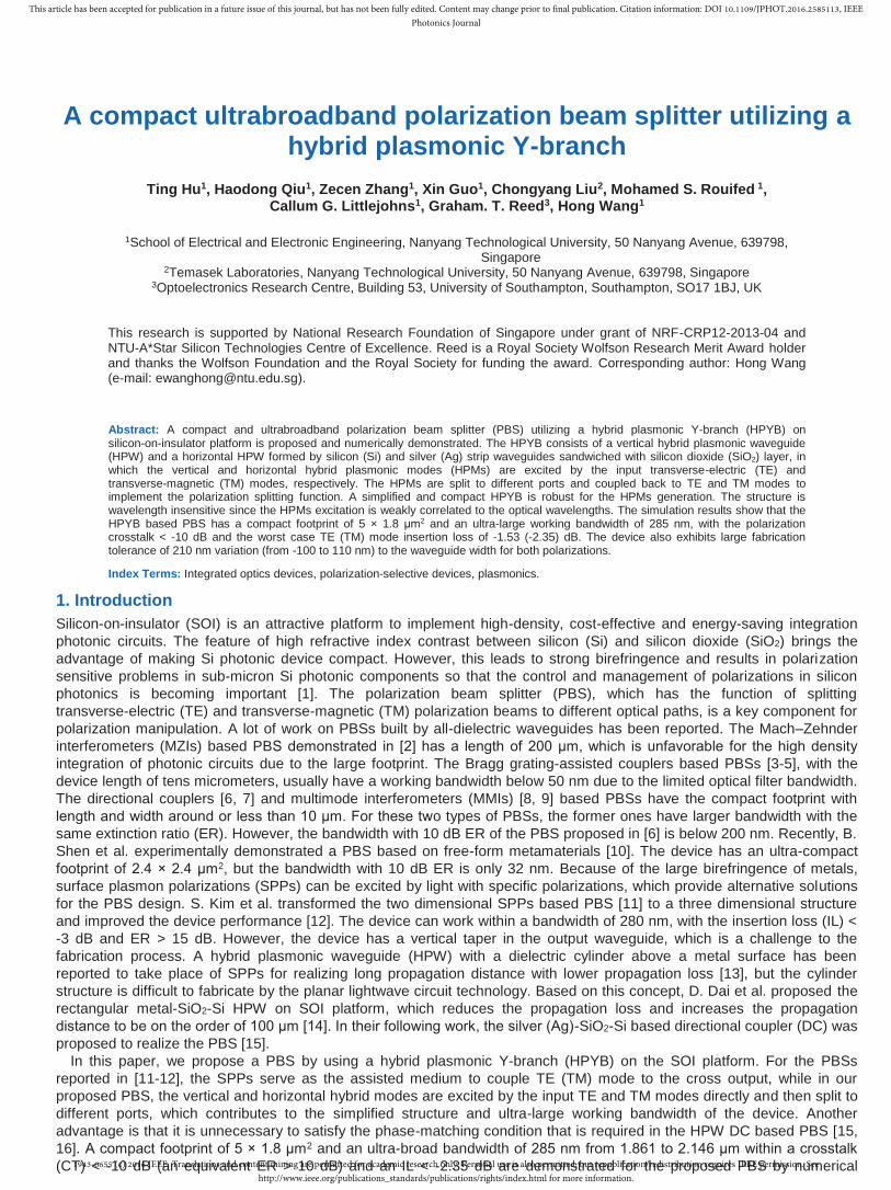
The schematic of the proposed PBS is shown in Fig. 1(a). The input section is a straight Si waveguide with the width of W
and height of H. Its cross section is shown in Fig. 1(c). The two bending Si waveguides have the same height with the input
waveguide and the radii of R1= R2=20 μm (shown in Fig. 1(b)).A vertical HPW is constructed on the right hand bending Si
waveguide sidewall in the form of an Ag strip and a slot SiO2 layer between them. As seen from Fig.1 (d), the width of Si, Ag
and SiO2 of the vertical HPW are denoted as Wv, WAg, and Ws, respectively. The left bending Si waveguide has an Ag strip
above it with an intermediate SiO2 layer which together form the horizontal HPW, the cross section of which is shown in Fig.
1(e). The height of SiO2, Ag, and the width of Si of the horizontal HPW are Hs, HAg and WH, respectively. The working
principle of the proposed PBS is as follows: The input light with TE polarization launched into Port 1 (P1) excites the hybrid
plasmonic mode (HPM) in the vertical HPW and then is guided to the output port 2 (P2), while the TM polarization light sent
into P1 excites the HPM in the horizontal HPW and transmits to the output port 3 (P3). The electrical fields of TE mode, TM
mode, vertical HPM and horizontal HPM are plotted as insets in Fig.1 (a). To characterize the device performance, the IL
and CT of different modes are defined as the following (expressed in dB):
10 2 110 log ( )TE TE
TEIL P P (1)
10 3 110 log ( )TM TM
TMIL P P (2)
10 3 310 log ( )TE TM
TECT P P (3)
10 2 210 log ( )TM TE
TMCT P P (4)
where PiTE (i=1, 2, 3) represents the optical power at port i with TE mode launched, and Pi
TM (i=1, 2, 3) is the optical power
at port i with TM mode injected. ILTE and CTTE are the IL and CT of TE mode. ILTM and CTTM represent the IL and CT of TM
mode. One can see from Eq. (3) and Eq. (4) that the absolute values of CTTE and CTTM are equal to the ER of P3 and P2,
respectively.
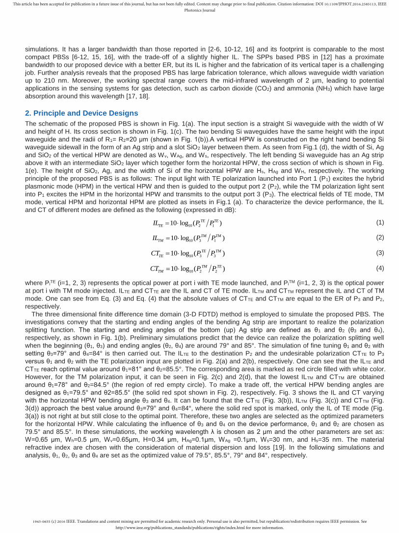
The three dimensional finite difference time domain (3-D FDTD) method is employed to simulate the proposed PBS. The
investigations convey that the starting and ending angles of the bending Ag strip are important to realize the polarization
splitting function. The starting and ending angles of the bottom (up) Ag strip are defined as θ1 and θ2 (θ3 and θ4),
respectively, as shown in Fig. 1(b). Preliminary simulations predict that the device can realize the polarization splitting well
when the beginning (θ1, θ3) and ending angles (θ2, θ4) are around 79° and 85°. The simulation of fine tuning θ1 and θ2 with
setting θ3=79° and θ4=84° is then carried out. The ILTE to the destination P2 and the undesirable polarization CTTE to P3
versus θ1 and θ2 with the TE polarization input are plotted in Fig. 2(a) and 2(b), respectively. One can see that the ILTE and
CTTE reach optimal value around θ1=81° and θ2=85.5°. The corresponding area is marked as red circle filled with white color.
However, for the TM polarization input, it can be seen in Fig. 2(c) and 2(d), that the lowest ILTM and CTTM are obtained
around θ1=78° and θ2=84.5° (the region of red empty circle). To make a trade off, the vertical HPW bending angles are
designed as θ1=79.5° and θ2=85.5° (the solid red spot shown in Fig. 2), respectively. Fig. 3 shows the IL and CT varying
with the horizontal HPW bending angle θ3 and θ4. It can be found that the CTTE (Fig. 3(b)), ILTM (Fig. 3(c)) and CTTM (Fig.
3(d)) approach the best value around θ3=79° and θ4=84°, where the solid red spot is marked, only the IL of TE mode (Fig.
3(a)) is not right at but still close to the optimal point. Therefore, these two angles are selected as the optimized parameters
for the horizontal HPW. While calculating the influence of θ3 and θ4 on the device performance, θ1 and θ2 are chosen as
79.5° and 85.5°. In these simulations, the working wavelength λ is chosen as 2 μm and the other parameters are set as:
W=0.65 μm, Wh=0.5 μm, Wv=0.65μm, H=0.34 μm, HAg=0.1μm, WAg =0.1μm, Ws=30 nm, and Hs=35 nm. The material
refractive index are chosen with the consideration of material dispersion and loss [19]. In the following simulations and
analysis, θ1, θ2, θ3 and θ4 are set as the optimized value of 79.5°, 85.5°, 79° and 84°, respectively.
1943-0655 (c) 2016 IEEE. Translations and content mining are permitted for academic research only. Personal use is also permitted, but republication/redistribution requires IEEE permission. Seehttp://www.ieee.org/publications_standards/publications/rights/index.html for more information.
This article has been accepted for publication in a future issue of this journal, but has not been fully edited. Content may change prior to final publication. Citation information: DOI 10.1109/JPHOT.2016.2585113, IEEEPhotonics Journal
Fig. 1 Schematic of the proposed PBS, (a) the 3D view (b) the top view, and the cross-section of (c) A-A’ (d) B-B’ (e) C-C’.
Since the hybrid structure used in the PBS takes both advantages of all-dielectric photonics and plasmonics for relatively
low loss and compact footprint, the thickness of the lower refractive index layer (SiO2) has a large effect on the device
performance. At the wavelength around 2 µm, the absorption loss of Ag is large indicated by Drude model [11]. The effect of
Ag on the HPMs should be neither too strong (inducing large IL) nor too weak (unable to excite the HPMs efficiently, in other
words, the HPMs will cut-off). An appropriate HPM can be obtained by controlling the thickness of SiO2 sandwiched in Si
and Ag. Fig. 4(a) shows the dependence of the IL and CT on the SiO2 width (Ws) of the vertical HPW. The CTTE to P3 is
found to be lower than -12 dB when Ws =22.5 nm, and the ILTE to P2 also approaches a relatively low value of -1 dB. For Ws
less than 22.5 nm, the absorption loss of the plasmonics increases with the decreasing Ws and leads to a larger IL. To the
contrary, when Ws is beyond 22.5 nm, the vertical HPM cannot be excited substantially by the incoming TE mode, and
consequently the IL increases. Meanwhile, the leakage of optical power to P3 results in a higher CTTE. A similar trend is
found for ILTM and CTTM in Fig. 4(a). We can that the performance deterioration rates of ILTM and CTTM are not as significant
as those of ILTE and CTTE when the Ws deviates from the optimal value of 22.5 nm. It indicates that the width of the vertical
slot SiO2 has a larger influence on the vertical HPM than the horizontal HPM. The IL and CT varying with the SiO2 thickness
(Hs) of the horizontal HPW are shown in Fig. 4(b). As seen in it, the optimal ILTM of -1.3 dB is obtained (with the CTTM of
-14.2 dB) at Hs = 32.5 nm. The ILTM and CTTM deteriorates while Hs deviate from 32.5 nm. The reason for it is the same as
that for the ILTE and CTTE deterioration caused by Ws variation. When Hs drifts from 32.5 nm, the modest change of ILTE and
CTTE coveys that the effect of the horizontal slot SiO2 thickness on the horizontal HPM is stronger than that on the vertical
HPM.
Fig. 2 IL and CT versus the vertical HPW bending angle θ1 and θ2. (a) ILTE and (b) CTTE with TE input mode; (c) ILTM and (d) CTTM with TM input mode.

1943-0655 (c) 2016 IEEE. Translations and content mining are permitted for academic research only. Personal use is also permitted, but republication/redistribution requires IEEE permission. Seehttp://www.ieee.org/publications_standards/publications/rights/index.html for more information.
This article has been accepted for publication in a future issue of this journal, but has not been fully edited. Content may change prior to final publication. Citation information: DOI 10.1109/JPHOT.2016.2585113, IEEEPhotonics Journal
Fig. 3 IL and CT varying with the horizontal HPW bending angle θ3 and θ4. (a) ILTE and (b) CTTE
with TE input mode; (c) ILTM and (d) CTTM with TM input mode.
Fig. 4 IL and CT varying with (a) Ws and (b) Hs.
The influence of the width/thickness of Ag sandwiched in Si and SiO2 on the IL and CT is simulated and analyzed. Fig. 5(a)
shows the IL and CT varying with the width of Ag beside the Si waveguide at the bottom arm of the HPYB. We can see that the ILTE and CTTE decrease with increasing TAg. They deteriorate drastically when TAg blow 50 nm. For TAg > 100 nm, they are almost consistent. The CTTM has an optimal value at TAg=50 nm, but its increase is very limited for TAg > 50 nm. The ILTM has little change over TAg, implying that TAg has larger influence on the vertical HPM than the horizontal HPM. Fig. 5(b) shows the IL and CT varying with the thickness of Ag above the Si waveguide at up arm of the HPYB. As seen from it, the ILTE is almost unaffected by changing HAg, while ILTM increases at first then decreases with increasing HAg. On the contrary to ILTM, the CTTE and CTTM decrease at first, then increase with increasing HAg. However, the changes in the magnitude are rather modest, even for HAg < 50 nm. Based on the simulation results, TAg and HAg are both chosen as 100 nm to make a trade-off. In this simulation, the optimized Ws = 22.5 and Hs = 32.5 nm are used, the other dimension parameters are set as those aforementioned.

1943-0655 (c) 2016 IEEE. Translations and content mining are permitted for academic research only. Personal use is also permitted, but republication/redistribution requires IEEE permission. Seehttp://www.ieee.org/publications_standards/publications/rights/index.html for more information.
This article has been accepted for publication in a future issue of this journal, but has not been fully edited. Content may change prior to final publication. Citation information: DOI 10.1109/JPHOT.2016.2585113, IEEEPhotonics Journal
Fig. 5 IL and CT varying with (a) TAg and (b) HAg.
The PBS is wavelength insensitive because the excitation of HPMs in the HPYB is weakly related to the input light
wavelengths. Fig. 6 illustrates the input wavelength dependence of the IL and CT for the PBS. An IL of -1 (-1.3) dB, CT of
-12.4 (-14.2) dB for the TE (TM) mode are obtained at the mid-infrared wavelength of 2 μm. The PBS keeps a CT<-10 dB
over an ultra-wide spectral range of 285 nm from 1.861 to 2.146 μm for the TE input mode. Maintaining the same CT, for the
TM mode, the working bandwidth is 409 nm from 1.82 to 2.229 μm. For shorter wavelengths, i.e. λ< 1.861 μm, the electrical
field confinement of the Si waveguide is becoming stronger, resulting in inefficient excitation of the HPMs by the launched
lights. It indicates that the HPMs will approach cut-off and are changing into the Si channel modes, which result in smaller
polarization selection. Consequently, the HPMs are unable to be split to different ports efficiently and result in the larger CT.
For longer wavelengths, i.e. λ> 2.146 μm, the electrical field confinement of Si waveguide becomes weaker. As a result, the
metal absorption deteriorates the device’s IL and CT. Hence, for the given CT<-10 dB, the proposed PBS is able to work
within an ultra-broad bandwidth of 285 nm, where the worst case ILTE and ILTM are -1.53 and -2.35 dB, respectively.
Fig. 6 Wavelength dependence of IL and CT with (a) TE input mode and (b) TM input mode.
In order to demonstrate the polarization splitting function with the optimized dimension parameters, the light propagation
of the designed PBS for TE (Ey) and TM (Ez) modes of input are simulated and shown in Fig. 7. One can see from Fig. 7(a)
that the input TE-polarization light excites the vertical HPM in the bottom arm of the HPYB. After a short distance
propagation through the HPW, the vertical HPM is coupled back to the TE-polarization Si strip waveguide mode and
subsequently transmits to P2. The corresponding Ey of cross-section B-B’ is shown in Fig. 7(b). It can be seen that, most of
the electric field is distributed in the SiO2 slot, which forms the vertical HPM. For the TM polarization (Fig. 7(c)), however, the
input light excites the horizontal HPM (the electrical field at cross-section C-C’ is shown in Fig. 7(d)) in the up arm, and then
it transforms back to the TM mode after passing through the HPW and propagates to P3. The simulation results clearly
indicate that such a compact HPYB is sufficient to ensure the two HPMs are generated and split to different ports. Based on
the values extracted from Fig. (7), the footprint of the PBS is estimated as 5 × 1.8 μm2 (x from 3 to 8 μm, y from -0.6 to 1.2
μm).

1943-0655 (c) 2016 IEEE. Translations and content mining are permitted for academic research only. Personal use is also permitted, but republication/redistribution requires IEEE permission. Seehttp://www.ieee.org/publications_standards/publications/rights/index.html for more information.
This article has been accepted for publication in a future issue of this journal, but has not been fully edited. Content may change prior to final publication. Citation information: DOI 10.1109/JPHOT.2016.2585113, IEEEPhotonics Journal
Fig. 7 (a) Light propagation and (b) electrical field at cross-section B-B’ with TE input mode; (c) Light propagation and
(d) electrical field at cross-section C-C’ with TM input mode.
3. Fabrication Tolerance Discussion
The experimental realization of Ag strip (using the Ag strip beside Si waveguide for instance) and Si waveguides is as
following: The Si waveguides will be patterned by electron beam lithography (EBL), followed by reactive-ion etching (RIE)
process. To fabricate the Ag strip in the vertical HPW, “lift-off” process could be employed. A 500 nm thick of PMMA layer
(950PMMA A7), which is a commonly used EBL positive resist with high resolution of sub-100 nm, will be deposited and
patterned by EBL. The next step is to deposit Ag film with a thickness of 340 nm by using electron beam evaporation. After
that, the sacrificial PMMA layer will be removed by PG remover or acetone, together with parts of Ag film covering it. The Ag
strip is therefore formed. During the device fabrication, the actual device dimension may deviate from the designed values
due to process variations and result in performance deterioration. The most probable dimension variation caused by the
fabrication error is the waveguide width in the etching processes. Here, the fabrication tolerance to the waveguide width
variation of the designed PBS is analyzed. We assume the width of the input waveguide (W), the bottom arm (W v) and the
up arm (Wh) of the PBS have the same deviation of ΔW induced by the fabrication error [15]. As shown in Fig. 8(a), an ILTE <
-2 dB and a CTTE < -10 dB for the TE polarization input mode are observed with ΔW ranging from -100 to 120 nm. The ILTE
and CTTE deteriorate as the absolute value of ΔW becomes larger. While for the TM polarization input, the device keeps the
IL < -2 dB and CT < -10 dB with ΔW fluctuating from -100 to 110 nm, as seen from Fig. 8(b). The fabrication tolerance of
210 nm variation to the waveguide width is larger than that of the all-dielectric waveguide and HPW based PBSs reported in
[3-6, 8, 9, 15], which ensures high robustness for the fabrication of the proposed device.
Fig. 8 Fabrication tolerance of the waveguide width variation ΔW with (a) TE input mode and (b) TM input mode.
4. Conclusions
In summary, a HPYB based PBS with the operating principle different from previous work has been proposed and
numerically demonstrated. The HPYB is constructed by two bending Ag-SiO2-Si HPWs. The influence of the starting/ending

1943-0655 (c) 2016 IEEE. Translations and content mining are permitted for academic research only. Personal use is also permitted, but republication/redistribution requires IEEE permission. Seehttp://www.ieee.org/publications_standards/publications/rights/index.html for more information.
This article has been accepted for publication in a future issue of this journal, but has not been fully edited. Content may change prior to final publication. Citation information: DOI 10.1109/JPHOT.2016.2585113, IEEEPhotonics Journal
angles of Ag strip waveguide and the thickness of Ag, SiO2 on the device performance has been analyzed by 3-D FDTD
method. With the optimized dimension parameters, the device exhibits an ultra-broad bandwidth of 285 nm with 10 dB ER,
while possesses a small footprint comparable to the most compact PBSs reported previously. Our numerical simulation has
also shown that the fabrication tolerance of the waveguide width is greatly enhanced as compared to other HPW and
all-dielectric waveguide based PBSs. These advantages enable wide potential applications of this PBS in SOI based
integrated photonic circuits within the near- and mid-infrared wavelength range.
Acknowledgements
The authors would like to thank Dr. Zhenfeng Zhuang for discussing on the 3D schematic diagram drawing.
References
[1] D. Dai, L. Liu, S. Gao, D. X. Xu, and S. He, “Polarization management for silicon photonic integrated circuits,” Laser Photon. Rev., vol. 7, no. 3, pp. 303-328, 2013.
[2] D. Dai, Z. Wang, J. Petters, and J. E. Bowers, “Compact polarization beam splitter using an asymmetrical Mach–Zehnder interferometer based on silicon-on-insulator
waveguides,” IEEE Photon. Technol. Lett., vol. 24, no. 8, pp. 673-675, 2012.
[3] H. Qiu, Y. Su, P. Yu, T. Hu, J. Yang, and X. Jiang, “Compact polarization splitter based on silicon grating-assisted couplers,” Opt. Lett., vol. 40, no. 9, pp.
1885-1887, 2015.
[4] T. Hu, M. S. Rouifed, H. Qiu, X. Guo, C. G Littlejohns, C. Liu, and H. Wang, “A polarization splitter and rotator based on a partially etched grating-assisted coupler,” IEEE Photon. Technol. Lett., vol. 28, no. 8, pp. 911-914, 2016.
[5] Y. Zhang, Y. He, J. Wu, X. Jiang, R. Liu, C. Qiu, X. Jiang, J. Yang, C. Tremblay, and Y. Su, “High-extinction-ratio silicon polarization beam splitter with tolerance
to waveguide width and coupling length variations,” Opt. Express, vol. 24, no. 6, pp. 6586-6593, 2016.
[6] Y. Xu and J. Xiao, “Compact and high extinction ratio polarization beam splitter using subwavelength grating couplers,” Opt. Lett., vol. 41, no. 4, pp. 773-776, 2016.
[7] D. W. Kim, M. H. Lee, Y. Kim, and K. H. Kim, “Planar-type polarization beam splitter based on a bridged silicon waveguide coupler,” Opt. Express, vol. 23, no. 2,
pp. 998-1004, 2015.
[8] X. Sun, M. Z. Alam. J. S. Aitchison, and M. Mojahedi, “Compact and broadband polarization beam splitter based on a silicon nitride augmented low-index guiding structure,” Opt. Lett., vol. 41, no. 1, pp. 163-166, 2016.
[9] A. Hosseini, S. Rahimi, X. Xu, D. Kwong, J. Covey, and R. T. Chen, “Ultracompact and fabrication-tolerant integrated polarization splitter,” Opt. Lett., vol. 36, no.
20, pp. 4047-4049, 2011.
[10] B. Shen, P. Wang, R. Polson, and R. Menon, “An integrated-nophotonics polarization beamsplitter with 2.4 × 2.4 μm2 footprint,” Nat. Photon., vol. 9, pp. 378-382,
2015.
[11] Q. Tan, X. Huang, W. Zhou, and K. Yang, “A plasmonic based ultracompact polarization beam splitter on silicon-on-insulator waveguides,” Sci. Rep., vol. 3, 2206,
2013.
[12] S. Kim and M. Qi, “Copper nanorod array assisted silicon waveguide polarization beam splitter,” Opt. Express., vol. 22, no. 8, pp. 9508-9516, 2014.
[13] R. F. Oulton, V. J. Sorger, D. A. Genov, D. F. P. Pile, and X. Zhang, “A hybrid plasmonic waveguide for subwavelength confinement and long-range propagation,”
Nat. Photon., vol. 2, pp. 496-500, 2008.
[14] D. Dai and S. He, “A silicon-based hybrid plasmonic waveguide with a metal cap for a nano-scale light confinement,” Opt. Express, vol. 17, no. 19, pp. 16646-16653,
2015.
[15] X. Guan, H. Wu, Y. Shi, L. Wosinski, and D. Dai, “Ultracompact and broadband polarization beam splitter utilizing evanescent coupling between a hybrid plasmonic waveguide and a silicon nanowire,” Opt. Lett., vol. 38, no. 16, pp. 3005-3008, 2013.
[16] Y. Ma, G. Farrell, Y. Semenova, H. P. Chan, H. Zhang, and Q. Wu, “Low loss, high extinction ration and ultra-compact plasmonic polarization beam splitter,” IEEE
Photon. Technol. Lett., vol. 26, no. 7, pp. 660-663, 2014.
[17] R. Soref, “Mid-infrared photonics in silicon and germanium,” Nat. Photon., vol. 4, pp. 495-497, 2010.
[18] J. J. Coleman, A C. Bryce, and C Jagadish, Advances in semiconductor lasers, (Elsevier, 2012).
[19] E. D. Palik, Handbook of Optical Constants of Solids, (Elsevier, 1997).