a cell set for self-timed design using actel fpgas
TRANSCRIPT

A Cell Set for Self-Timed Design using Actel FPGAs
Erik Brunvand
UUCS-91-013
Department of Computer Science University of Utah
Salt Lake City, UT 84112 USA •
August 10, 1991
AbstractAsynchronous or self-timed systems that do not rely on a global clock to keep system
components synchronized can offer significant advantages over traditional clocked circuits in a variety of applications. However, these systems require that suitable self-timed circuit primitives are available for building the system. This report describes a cell set designed for building self-timed circuits and systems using Actel field programmable gate arrays (FPGAs). The cells use a two-phase transition signalling protocol for control signals and a bundled protocol for data signals. This library of macro cells is designed to be used with the Work view tool suite from VIEW logic and the Action Logic System (ALS) from Actel.

As VLSI technology improves, the systems that can be built become larger, faster, and more complex. Along with these improvements, however, come many problems directly associated with the speed and scale o f the new systems. In particular, timing problems become severe and account for more and more o f the design and debugging expense. A major culprit is the traditional synchronous design style in which all the system components are synchronized to a global clock. One solution is to use asynchronous or self-timed [13] techniques. Self-timed circuits avoid clock-related timing problems by enforcing a simple communication protocol which is insensitive to delays in circuit components or the wires that arc used to connect them.
The design o f asynchronous or self-timed circuits and systems has long been considered too difficult by all but a few researchers and engineers. One reason for this perception is that a long history o f designing synchronous circuits has resulted in a great deal o f knowledge and large variety o f tools to aid in that style o f circuit design. The same level o f support for asynchronous design does not exist at present. Because there is no great demand for these circuits, semiconductor manufacturers do not offer commercially available parts that are suitable for asynchronous design. This only reinforces the tendency to design traditional synchronous systems.
Asynchronous design is, however, currently attracting renewed interest as a method for coping with some o f the problems associated with improved VLSI technology. The
1 Introduction

2 ERIK BRUNVAND
lack o f commercially available parts can be largely overcome simply by designing the needed parts directly in custom VLSI. The size penalty for individual circuits is becoming less severe as device size shrinks and die size increases, and while the individual circuit modules may still be more difficult to design than their synchronous counterparts, the more serious problem o f system integration can be made much easier.
While the necessary circuits for self-timed design can be built in custom VLSI, the turnaround time for these chips is still too long to allow rapid prototyping and experimentation with novel systems. Field programmable gate arrays (FPGAs) offer an excellent alternative for rapid development o f novel systems provided suitable circuit structures can be implemented. These FPGA systems can be used directly, or replaced with faster or smaller custom VLSI designs after the prototype has been evaluated.
This report presents a library o f macro cells suitable for designing self-timed systems using Actel field programmable gate arrays [9,1]. The operation o f the circuits and a description the library are presented, followed by some brief examples.
1.1 Self-Timed Circuits
Some o f the main reasons that self-timed circuits are an attractive alternative to traditional synchronous circuits are:
Timing Self-timed circuits separate timing from functionality. Rather than synchronize the entire system to a global clock signal, self-timed circuits localize timing information to individual circuits and avoid the standard problems o f clock distribution and clock skew.
Composability Systems may constructed by connecting components and assembling subsystems based only on their functionality rather than having to consider their timing characteristics. Increased composability can greatly decrease the time required to assemble a new system.
Robustness Because timing is separated from functionality, large self-timed systems can be built from subsystems that operate at widely different speeds, or that will continue to operate over a wide range o f voltage or temperature conditions.
Incremental Improvement In a properly designed asynchronous system it is possible to improve the performance or functionality o f a system by improving or replacing individual subsystems incrementally without changing or retiming the whole system.
Performance Traditional synchronous systems usually exhibit worst case behavior while asynchronous systems tend to reflect the average case.
Hierarchical Structure The designer is able to deal with large systems hierarchically. Each subsystem can be designed and tested independently with confidence that,

A CELL SET FOR SELF-TIMED DESIGN USING ACTEL FPGAS 3
because a self-timed communication protocol is used, they will operate correctly when assembled into a larger system.
Although self-timed circuits can be designed in a variety o f ways, the circuits considered here predominantly use two-phase transition signalling for control and a bundled protocol for data paths. Two-phase transition signalling [13] uses transitions on signal wires to communicate. Only the transitions are meaningful; a transition from low to high is the same as a transition from high to low and the particular voltage on each wire is not important. The communication protocol uses two wires called Req and Ack to request service, and acknowledge completion respectively.
A bundled data path uses a single set o f control wires to indicate the validity o f a bundle o f data wires. This requires that the data bundle and the control wires be constructed such that the value on the data bundle is stable at the receiver before a signal appears on the control wire. This condition is similar to, but weaker than, the equipotential constraint [13].
The circuit modules used here are based on those already implemented in CMOS and described elsewhere [5,4,16,15].
1.2 Using Workview
This cell set is designed to be used with the Workview suite o f tools from VIEW logic. In particular, these instructions are based on Workview version 4.1. This section contains a brief introduction to using Workview and some details about using the asynchronous cell library. The manuals give more complete information about the use o f the tools [17].
Before starting Workview, some environment variables must be set and the Workview directory must be added to your path. Our version o f Workview currently only runs on Sun SPARC machines. To access the program add
/n/vlsi/usr/vlsi/viewlogic
to your search path.Now some environment variables must be set to let Workview know where to
look for things. Set these variables using the setenv command. If you plan to use Workview frequently, you should probably set these variables in your .cshrc file so they will be set automatically. The required variables are:
FC)NT1=6x10 FONT2=8x13 FONT3=9x15 WDIR=.:/n/vlsi/usr/vlsi/viewlogic/standard

4 ERIK BRUNVAND
The font variables are required so that Workview can use the X window system display, and the W DIR variable points to the standard user interface. If Workview is used for analog circuits, a different user interface is required. See the Workview manual for details.
Now that the environment variables are set, the program may be started by invoking workview from the shell. If the window appears and then disappears citing an “ SEC error” this means that the license server is not running and needs to be restarted.
Now that Workview is accessible there are a variety o f options that can be changed by changing the initialization file. This file is called viewdraw.ini and should live in your design directory. The best bet is to copy the system default viewdraw.ini file and make any changes that are desired. All o f the changes are optional except for specifying the library search path. This will let viewlogic know where to find the Actel and async libraries. In order to use these libraries you should add the following lines to the end o f your viewdraw.ini file.
DIR [p ].DIR [r] /n/vlsi/usr/vlsi/viewlogic/lib/async DIR [r] /n/vlsi/usr/vlsi/als/lib/a1000/cells DIR [r] /n/vlsi/usr/vlsi/als/lib/a1000/models DIR [r] /n/vlsi/usr/vlsi/viewlogic/lib/builtin (builtin)
The directory marked [p] is the primary design directory. The indicates that the current working directory is where the primary design files will be stored. Secondary design directories that can be read and written should be specified using [w]. Directories marked with an [r] are read-only library directories.
The async directory is the asynchronous cell library. All the cells discussed later in this report are available in this directory. The cells directory contains the macro cells distributed by Actel and described in the Actel databook [1], If your design includes cells from the Actel library, this is the directory to look in. Also, if you need to create macros that are not contained in the async library, your building blocks should come from this directory.
The last two directories, models and builtin, are basic cells that the previous two directories are built on. If your goal is an Actel FPGA you should NOT use macros from either o f these two directories! An Actel part cannot be generated if you use cells from these directories.
2 The Actel FPGA ........ ̂ . .....
The Actel product is a non-reusable field programmable gate array implemented in 2.0u or 1.2/i CMOS. The chip is arranged much like a conventional gate array with a

S O .
A CELL SET FOR SELF-TIMED DESIGN USING ACTEL FPGAS 5
S 1
Figure 1: Actel Basic Logic Module
Table 1: Actel Chip Sizes
Device Series Logic Modules Package Type User I/OsA1010 295 68 PLCC 57A 1020 547 84 PLCC 69
rows o f logic cells interspersed with routing channels. However, these routing channels are not simply empty space there the wire may be run, as in a mask programmable gate array. The routing channels on an Actel chip contain predefined wire segments o f various lengths. These wire segments may be connected through a two-terminal electrically programmable device known as an “ anti-fuse.” This anti-fuse is a device that irreverseably changes from a high to a low resistance when “ blown” by applying an appropriate voltage. Logic modules are connected to perform the desired function by blowing selected anti-fuses and thus programming the chip to a specific function. Once programmed, an Actel FPGA cannot be changed or re-programmed.
The basic logic module is an eight input, single output, device chosen to be small and flexible and at the same time be a good match for the wiring resources available on the chip. The basic module is shown in Figure 1. This module is the basis for all the macros in the Actel cell library as well as the macros in the async library.
Chips from Actel contain some number o f these logic modules, a collection o f wiring segments, anti-fuses to connect those segments, and a set o f programmable I/O pads. Examples o f two common sizes o f Actel parts are given in Table 1.

ERIK BRUNVAND
BJ~c)aUT̂ c)sOTaJc)s'g ~ c > ~UT H (—'̂ VjUT
R 1 «
Al
R2_A2
-L
R l ,A l RS "
AS R2 A2__
R3- A3
BMP L REQ ■̂ PROBE TOU,I1Q — S e l L e c t
CNIT FOU1SNEXT CLR----- 1------ O----
:all
3
_LSMPL REQ-̂ PROBK TOUT1Q —S e l_ e o t
FOUl SNEXT CLR---- 1-------O----
—rrcR—OUTF _ s u w
OUTF — TOGGLE
SELECT S ELECT OUT OI N XN INOUTT OUTT OUT 1
SELi 3LR =LR
R 1_ Al_
Rfi R2< AS A2_
R3_A3
R4_ A 4
=all
4 _RSAS
In / D » X a y - T \ o U T
i n/ 0«» 1 *»y- lAoUT i n/ Delay-2'\0UT IN/* Del ay-3'\0U_ ^ J — \ J — 11 — »
I____L
:cs-Inar Bit a
DT L N O
►►p
jILNT
Figure 2: Macro Library for Self-Timed Designs
3 A Cell Library
This macro library has been developed to allow these circuits to be implemented using Actel FPGAs. Schematic symbols for each o f the cells in this library are shown in Figure 2. These macros can be placed in schematics using the ViewDraw tool inside Workview. Select add component from the Workview menu and select cells from the async directory. These modules are all implemented in terms o f the macro library provided by Actel [1], and have been implemented and tested for functionality.
It is not strictly necessary for the user o f this library to know how they are implemented in terms o f low level Actel macros. Implementations are given in this report to let the curious reader know how the modules are constructed and to give some ideas about implementation so that users can extend the library as they require more specialized macros cells in their own designs.
Actel FPGAs have fan-in and fan-out restrictions on the basic modules that must be met for best performance. Because some o f the macro cells in the async library have input signals tied to multiple Actel basic module inputs, descriptions o f the macro cells list the number o f input loads presented by each async macro input signal. Also, many o f the async macros have internal feedback to the same cell. This means that an async macro output may already be driving some number o f module inputs. This number is also reported in the description o f the async macro cells.
The number reported as input fan-in is the number o f Actel module inputs that are

A CELL SET FOR SELF-TIMED DESIGN USING ACTEL FPGAS 7
Figure 3: Exclusive-Or (XOR) gates
being driven off o f that input signal. The number reported as output fan-out is the number o f Actel module inputs that are already being driven by that macro output. Note that this number may be 0 which simply means that the output is not driving any extra inputs in that same macro.
The number o f basic Actel logic modules used to implement each o f the async library modules is also given in the table for each module.
3.1 Control Modules
Control modules all use two-phase transition signalling, and may include an active- low clear signal to reset any internal state in the module. Descriptions are given followed by a schematic o f the library implementation, and a table o f the I/O characteristics o f the module.
3.1.1 XOR gates
Exclusive-Or (XOR) gates are used frequently in two-phase circuits. One way to use an XOR is as an “ OR” gate for transitions. That is, a transition on either o f the inputs o f the gate will produce a transition at the output o f the gate. Another way to use an XOR is to generate a level signal from a pair o f transition signals. This is most commonly used with the Req and Ack wires o f a two-phase communication handshake. When the two wires are in the same state, whether that state is logic high or logic low, the communication is in an inactive state, and the next transition event must occur on the Req wire. When the two signals are in different states then there is an outstanding request that has not yet been acknowledged. An XOR gate can easily
. decode these two phases o f the communication protocol. An XOR gate with multiple inputs generalizes to a Parity gate which can be implemented by cascading multiple two-input XOR gates.
XOR gates are provided by the Actel standard macro library in two flavors as shown in Figure 3. These macros are called xor and xnor and are found in the cells library from Actel. The I/O information is shown in Table 2.

8 ERIK BRUNVAND
Table 2: XOR I/O SpecificationsName Description modules Input Fan-In Output Fan-Outxor Exclusive-Or gate 1 A 2
B 1Y 0
xnor Inverting XOR gate 1 A 2 B 1
Y 0
3.1.2 C -Elements
A C-element is used as the “ AND” function for transitions. A transition will occur at the output o f the gate only when there have been transitions at both o f the inputs to the gate. This use o f a C-element requires that the inputs to the gate be in the same state after initialization.
Another use for this gate is to wait until all the input signals are in the same state. For example, the two-input version o f this gate will force its output low when both inputs are low. The output will stay low until both o f the inputs are high at which time the output also goes high. If the inputs are in opposite states, the output holds its last value. A C-element generalizes to a multiple input gate where all o f the inputs must be in the same state before the output follows. C-elements with multiple inputs can be built simply by cascading two-input gates.
Two forms o f C-elements are implemented in the library; gates with a clear signal to reset the internal state, and gates without the clear signal. Also, inversions are available on one o f the inputs to the gates. The implementation o f a representative version o f each o f these types o f C-element is shown in Figure 4. The C-element without the clear signal is shown at the top o f the figure and is implemented using a single Actel module. If a clear signal is desired, a second Actel macro can be used to reset the output and the internal state o f the C-element when the active-low clear signal goes low.
The fan-in and drive characteristics o f each type o f gate is summarized in Table 3.
3.1.3 Call Modules
. A transition Call module implements the hardware equivalent o f a subroutine call. In response to a transition on either o f the two request lines R1 or R2, the Call module starts a “ subroutine” process with the Rs signal. The process making a request to the Call module is known as a client o f that Call module. When the subprocess completes and acknowledges with As, the Call module acknowledges the appropriate client on AI or A2. It is the responsibility o f the Call module to remember which o f R1 or R2 made the request so that the acknowledge gets routed to the correct client.
A full request-acknowledge transaction must be completed before either side may request again and the input request signals must be mutually exclusive. A Call

Figure 4: Two Forms of A C-Element
Table 3: C-element I/O SpecificationsName Description modules Input Fan-In Output Fan-Outc-elem Two-input C-element 1 A 2
B 1Out 2
c-elem-a C-element, inversion on A input
1 A 2 B 1
Out 2
c-elem-b C-element, inversion on B input
1 A 1 B 2
Out 2
c-elem-mc Two-input C-element with clear
2 A 2 B 1
Clr 1
Out 2
c-elem-mca C-element, inversion on A, with clear
2 A 2 B 1
Clr 1
Out 2
c-elem-mcb C-element, inversion on B, with clear
2 A 1 B 2
Clr 1
Out 2

10 ERIK BRUNVAND
RlA1
R l
A1
R2
A2
A2
Figure 5: A Transition Call Module
module can generalize to any number of client request/acknowledge pairs, but a Call with only a single input pair is simply a pair of wires connecting the input request to the subroutine request and subroutine acknowledge to input acknowledge. The arrow in the Call module’s symbol indicates the direction of the Call. That is, requests are routed to the subroutine along the direction of the arrow.
The library implementation of a Call module uses XORs and C-elements as shown in Figure 5. Note that the C-elements used in the Call module do not have a clear signal. It is assumed that when the circuit is initialized all the request signals to the Call will be forced low and thus the outputs of the Call will also go low.
The library versions of the three-client and four-client Call modules are constructed from cascaded two-client Call modules. The three-client Call is shown in Figure 6 and the four-client Call is constructed similarly. The three-client Call can also be implemented directly. This version of the three-client Call, named call3a uses fewer Actel modules, but has higher fan-in on the input signals. The implementation is shown in Figure 7. As this example shows, there are many ways to implement these asynchronous modules. The best implementation of a particular module depends on the restrictions of the circuit being built.
The I/O characteristics of the Call modules are shown in Table 4. The input Rn means any request signal, and the output An means any of the acknowledge signals to the clients.
3.1.4 Select Modules
A two-way transition Select module will steer an input transition to either of two outputs depending on the value of a Boolean data signal. This Boolean data signal, called sel, is a bundled data signal that uses the transition input tin as its control signal. That is, the sel signal must be valid from before a transition occurs on tin until after an output transition is generated at one of the outputs. Note that because the Select module reads, but does not write, the value of the bundled Boolean, the bundling constraint is a constraint on the environment. The environment must avoid making

Figure 7: Another Three-Client Call Module

12 ERIK BRUNVAND
Table 4: Call Module I/O SpecificationsName Description modules Input Fan-In Output Fan-Outcall2 Two-input Call 5 Rn 4
As 3An 2 Rs 0
call3 Three-input Call 10 Rn 4 As 3
An 2 Rs 0
ca!13a Three-input Call Smaller version
9 Rl 5 R2 6 R3 5 As 7
An 2 Rs 0
cal!4 Four-input Call 15 Rn 4As 3
An 2 Rs 0
Table 5: Select Module I/O SpecificationsName Description modules Input Fan-In Output Fan-Outselect Two-way Transition
Select Module4 In 3
Sel 2 Clr 4
OutT 2 OutF 3
a transition on tin until after the Boolean sel bit is valid. There is no way that the select module itself can enforce this constraint. A transition Select module will clear its internal state and force its outputs to low on a clear signal.
The library implementation of the select module is shown in Figure 8 and uses XOR gates and simple latches from the Actel macro library. The I/O characteristics are summarized in Table 5. There are two forms of selector in the async library. The only difference is cosmetic. One form has the false output on the top and the other has the true output on the top. This is strictly for ease in assembling schematics.
3.1.5 Q-select ModulesThis module is like a Select module except that it is delay-insensitive: there is
no bundling constraint on the sel signal. This means that the select signal might be changing when the input request occurs which, in turn, means that a special circuit must be used to sample the input that might be changing. In the CMOS version of the async library, the special circuit used to sample the sel signal in a Q-Select is a circuit known as a Q-fiop [12]. A Q-flop is a circuit that allows the value of a signal to be sampled on request, and generates an acknowledge when a reliable data value is available at the output. Because the sampling circuit may enter a metastable state, the acknowledge must be delayed until the circuit has exited metastability and a reliable

A CELL SET FOR SELF-TIMED DESIGN USING ACTEL FPGAS 13
OUTFSSLECTIHOUTT
SLR
result is reported.A Q-flop is a form of Arbiter and is easily built using custom VLSI. Unfortunately,
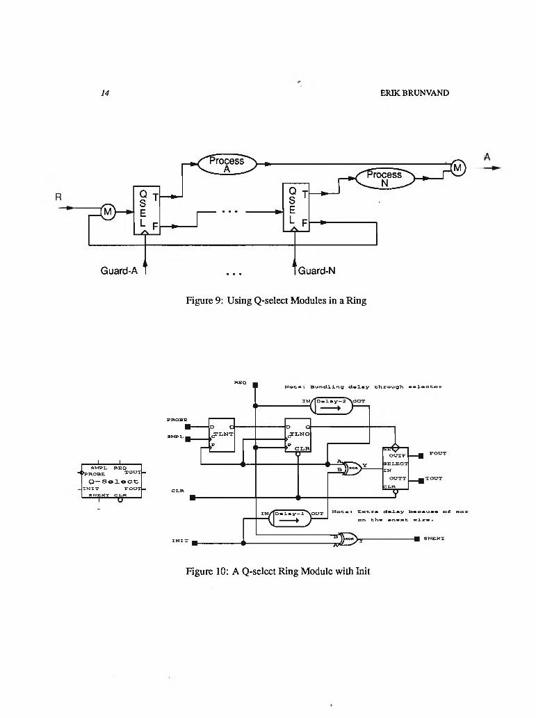
it is not possible to build such a circuit using the Actel basic module. For this cell library an approximation of a Q-select is implemented that requires that the Q-selects be used in a ring to test values from a set of sel signals in round robin fashion. In these modules the sel signal is known as probe to distinguish it from a bundled sel signal. A probe may be changing at any time, even when it is being tested. An example of this type of circuit is shown in Figure 9. The signals marked as guard in the figure are connected to the probe signals of the Q-select modules and indicate whether the associated process is ready to execute. The loop is started with a Req signal. This lets the Q-select modules begin checking each of the guards in turn. When a guard evaluates to True, the associated process is executed. If no guards are True, the loop continues checking until a guard becomes True.
The library contains circuits for two different forms of Q-select ring modules which are shown in Figures 10 and 11. They both operate in the same way, but the circuit in Figure 10 has additional circuitry to start the loop operation.
Both Q-select modules use a pair of transition latches to sample their probe signals. The first latch captures the value of the probe when it receives a transition on the smpl signal. This signal is produced by the previous Q-select in the ring. In fact, it is the Req to the previous Q-select. After the previous Q-select has finished its processing, it passes control to the next Q-select which transfers the value from the first latch to the second latch. The time interval between capturing the value in the first latch, and passing that value to the second latch should be enough time to assure that the first latch has exited metastability and the value has been reliable sampled. Of course, this cannot be guaranteed. There is still a minute chance that this circuit will fail to sample
ERDCBRUNVAND
Guard-A T Guard-N
Figure 9: Using Q-select Modules in a Ring
Figure 10: A Q-select Ring Module with Init

A CELL SET FOR SELF-TIMED DESIGN USING ACTEL FPGAS 15
SMPL REQ -tPROBE TOU1Q -S e lect
roui SNEXT CLRT "O"
o c^JLNT
Mete: Bundling clwltty fo
D «l«y -2 ^ 0 a T
■•lteter
s»CLRTT OUTF
SELECTIN
OUTT
SLR
Figure 11: A Q-select Ring Module
Table 6: Q-select Module I/O SpecificationsName Description modules Input Fan-In Output Fan-Outqsel-init Q-select with init 11 Req 3
Probe 2 Smpl 2 Clr 5 Init 3
TOut 2 FOut 3 Snext 0
qsel Q-select 8 Req 2 Probe 2 Smpl 2 Clr 5
TOut 2 FOut 3 Snext 2
the value reliably. A calculation using the delays through the Actel macros, the length of the shortest path from one Q-select to the next in the loop, and the metastability report in the Actel databook [1 ] indicate that the chance for failure is extremely small. Once the value is sampled reliably in the second latch, the standard Select module can produce a transition on the OutT or OutF output depending on the probe's value.
The first Q-select in the ring must include extra circuitry to start the operation of the ring. Shown in Figure 10, this module will inject a transition into the ring on an init signal to start checking the probe signal with the following Q-select.
An example of connecting these modules in a loop to check three probe signals is shown in Figure 12. In this circuit, three probe signals are checked by the Q-selects in the ring. The loop is started by a transition on the Req line. The Q-selects then proceed to test each probe in turn. If a probe is True, the associated process is executed and the circuit acknowledges, if the probe is False, control is passed to the next Q-select in


18 ERIK BRUNVAND
Table 8: Delay Module I/O SpecificationsName Description modules Input Fan-In Output Fan-OutDelay-N An N-Module Delay N In 1 Out 0
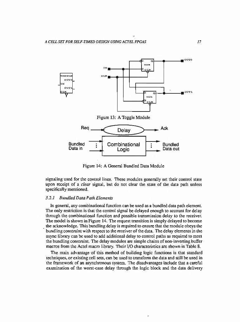
to the receiver is required to guarantee that the bundling constraint is met under all conditions. Guaranteeing that the bundling constraint is met under a variety of different power supply characteristics, temperature ranges, and process variations will often require the bundling delay to be large compared to the average case performance of the logic. This not only slows down the module, but also the entire system that uses this module.
Rather than relying on a delay model of the worst case path through the circuit, there are a variety of methods for generating self-timed logic [13,8,2,14]. Self-timed logic will signal when its output has been computed rather than simply producing a result at some time the future. All these methods use a multiple wire protocol with four phase signaling, commonly known as dual-rail protocol, for passing data to and from the combinational logic in a delay-insensitive way. Conversion between dual-rail and bundled protocols is simple [13, 5] so these self-timed logic techniques can be used even in a system that is largely bundled.
The main disadvantage of these self-timed logic techniques is an overhead in circuit area and the number of wires needed. Self-timed logic requires larger and more complicated circuit structures to implement a given logic function and the dual-rail protocol uses twice as many wires as the bundled implementation. For example, because dual-rail takes more wires, and pins are a very limited resource on a chip, if dual-rail signaling is used internal to the chip, then it may make sense to convert to a bundled protocol when sending data off the chip.
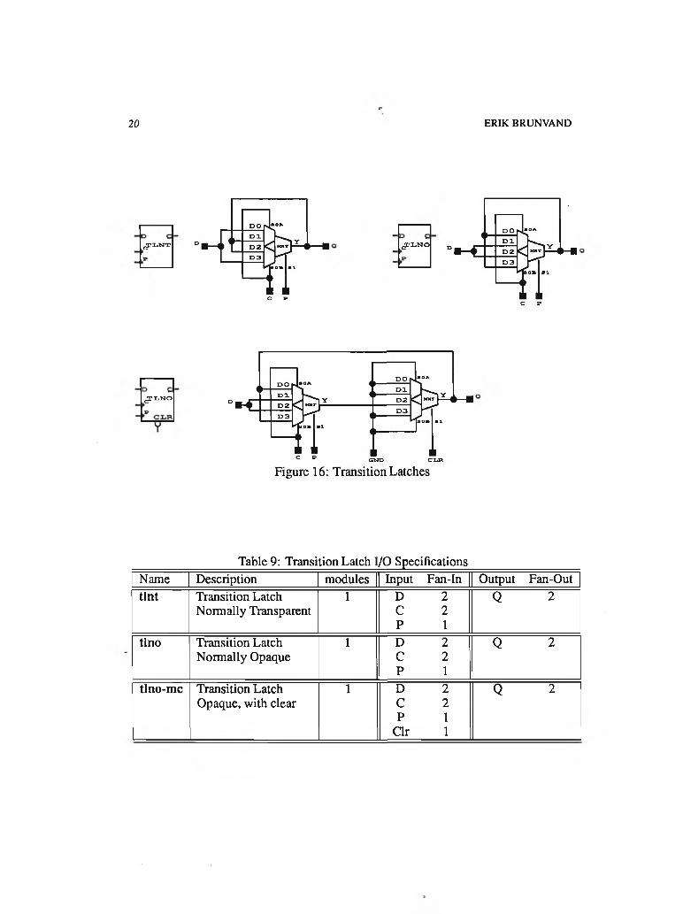
3.2.2 Transition Latches
A transition latch is a circuit that will capture and store bundled data signals in response to transition control signals. That is, on each transition of a control line a new value will be captured. An example of a possible implementation of one of these modules is shown in Figure 15. Note that this is not an Actel circuit. It is drawn here only as an aid to understanding the function of a transition latch. This is a latch which uses enabled inverters to form the loops that capture bundled data signals. The control signals for this module are called C for capture and P for pass. After initialization, when the two control signals are at the same level, the latch is transparent from input to output. The first transition occurs on the C signal which causes a loop to form either at the top or bottom of the circuit in Figure 15 to hold the value of the data signal. When a transition occurs on the P line, the loop is broken and the input is once again connected to the output. A latch of this form, where the first signal transition must be C is know as a normally transparent transition latch [5].

A CELL SET FOR SELF-TIMED DESIGN USING ACTEL FPGAS 19
< b
< FFigure 15: An Implementation of a Transition Latch (Normally Transparent)
Variations of this basic latch are easily imagined. Rather than be transparent when the input signals are at the same levels, the latch could be opaque in that initial state by exchanging some of the control signals. In this case, the first signal to the latch must be a P transition to allow the new input value through the latch, followed by a C transition to form an inverter loop and capture that value. This is known as a normally opaque transition latch.
These transition latches can be connected in groups to form transition registers. These registers are simply groups of latches with their C and P signals connected in parallel.
The transition latch shown in Figure 15 may be implemented using a single Actel module as shown at the top left of Figure 16. Because this is the normally transparent form of a transition latch, no clear signal is required. A normally opaque form of transition latch is shown at the top right of the figure. If a normally opaque form is used and a clear signal is desired a second Actel module can be used in the same way as in the C-element of Figure 4. This is seen at the bottom of Figure 16. The I/O characteristics of the latches are shown in Table 9.
3.2.3 Carry Completion Adder
One data path function that seems essential in any real system is addition. A simple way to implement addition in a self-timed system is to treat addition as a combinatorial function and build a general bundled module around that function. Any particular implementation of an addition operation might be used from ripple-carry addition to full carry-lookahead addition. The challenge is to identify the worst-case path through the resulting circuit and use the timing of that path to develop a delay model that meets the bundling constraint. The problem is that for a function like addition, the difference between the best-case delay, average delay, and worst-case delay may be dramatic, resulting in huge speed penalties in most cases because the
20 ERIK BRUNVAND
L̂NT T̂LNO
jJ'LNO
Table 9: Transition Latch I/O SpecificationsName Description modules Input Fan-In Output Fan-Outtint Transition Latch
Normally Transparent1 D 2
C 2 P 1
Q 2
tlno Transition Latch Normally Opaque
1 D 2 C 2 P 1
Q 2
tlno-mc Transition Latch Opaque, with clear
1 D 2 C 2 P 1
Clr 1
Q 2
A CELL SET FOR SELF-TIMED DESIGN USING ACTEL FPGAS 21
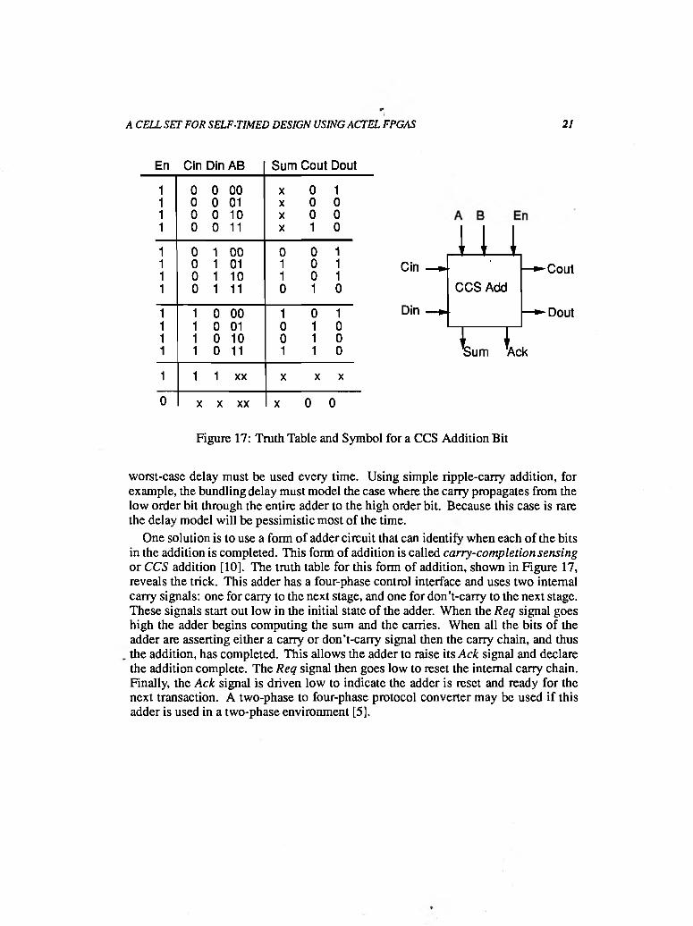
Figure 17: Truth Table and Symbol for a CCS Addition Bit
worst-case delay must be used every time. Using simple ripple-carry addition, for example, the bundling delay must model the case where the carry propagates from the low order bit through the entire adder to the high order bit. Because this case is rare the delay model will be pessimistic most of the time.
One solution is to use a form of adder circuit that can identify when each of the bits in the addition is completed. This form of addition is called carry-completion sensing or CCS addition [10]. The truth table for this form of addition, shown in Figure 17, reveals the trick. This adder has a four-phase control interface and uses two internal carry signals: one for carry to the next stage, and one for don’t-carry to the next stage. These signals start out low in the initial state of the adder. When the Req signal goes high the adder begins computing the sum and the carries. When all the bits of the adder are asserting either a carry or don’t-carry signal then the carry chain, and thus the addition, has completed. This allows the adder to raise its Ack signal and declare the addition complete. The Req signal then goes low to reset the internal carry chain. Finally, the Ack signal is driven low to indicate the adder is reset and ready for the next transaction. A two-phase to four-phase protocol converter may be used if this adder is used in a two-phase environment [5].

22 ERIK BRUNVAND
GNDFigure 18: A Carry Completion Adder Bit
The library implementation of one bit of the carry completion adder is shown in Figure 18. The Boolean expressions for the outputs of the adder are:
Sum = ((A © B) A Req) © CinCout = Req A (A A Cin + B A Cin + AAB)Dout = Req A (A ADin + B A Din + A AB)
A self-timed addition module can be constructed using a CCS adder bit module. The modules are chained together with the Cout and Dout of one stage connected to the Cin and Din of the next. The En signals from each bit of the adder are connected together and become the request line, and the acknowledges from each bit of the adder are connected into a tree of Join, or C-element, modules to signal the condition that all the adder bits have cleared, and that all the adder bits have produced their carry. The CCS adder module constructed in this fashion is shown in Figure 19. The rising En transition initiates addition by allowing each bit to compute its sum and carry. The rising Ack indicates that each bit has finished computing its carry to the next stage, and thus that the addition is complete. A falling En transition is required to initialize the CCS adder for the next addition by pulling all the carry signals low, and the falling Ack indicates that each bit is reset and the CCS adder is ready to compute a new result. Note that this adder only checks for completion on two out of the four bits. This is a compromise to decrease the number of modules used. A more conservative design would use completion detection on all the bits of the adder. Also, C-elements could be used for completion detection rather than AND and OR gates. This would allow the clearing phase of the adder to be checked as well as the addition phase. The four-bit

A CELL SET FOR SELF-TIMED DESIGN USING ACTEL FPGAS 23
A [ O l 3 ]
S U M [ O i 3 ]
Figure 19: A Four-Bit Carry-Completion Adder
Table 10: Cany Completion Adder I/O SpecificationsName Description modules Input Fan-In Output Fan-Outcca-bit Carry Completion
Adder Bit5 A 5
B 5 Cin 2 Din 1 En 6
Sum 0 Cout 0 Dout 0
cca-4 Four-bit CCS Adder 22 A-n 5 B-n 5 Cin 2 Din 1 En 1
Sum-n 0 Cout 1 Dout 2 Ack 0
adder segment in the async library can be stacked to make a larger adder of whatever size is desired.
3.2.4 Carry Completion Incrementer and Decrementer
If the desired function is simply to increment or decrement a value, a full adder may not be required. For these cases, macros to implement carry completion increment and decrement are provided that use fewer Actel macros. These cells operate in the same way as the adder, but always increment or decrement their single input value. The implementations are shown in Figures 20 and 21 and I/O information is in Table 11. These increment and decrement bits are also collected into four-bit modules for easy assembly into larger units.

24 ERIK BRUNVAND
Figure 20: A Carry Completion Increment Bit
Figure 21: A Carry Completion Decrement Bit
Table 11: Carry Completion Incr/Decr I/O SpecificationsName Description modules Input Fan-In Output Fan-Outccs-incr-bit Cany Completion
Increment Bit3 In 4
Cin 3 Din 1 En 3
Sum 0 Cout 0 Dout 0
ccs-incr-4 Four Bit Incrementer
14 In-n 4 Cin 3 Din 1 En 1
Sum-n 0 Cout 1 Dout 1
ccs-decr-bit Carry Completion Decrement Bit
3 In 4 Cin 4 Din 1 En 2
Sum 0 Cout 0 Dout 0
ccs-decr-4 Four Bit Decrementer
14 In-n 4 Cin 4 Din 1 En 1
Sum-n 0 Cout 1 Dout 1

A CEIL SET FOR SELF-TIMED DESIGN USING ACTEL FPGAS 25
BufferReq
AChannel Ack
BRec* Channel
DataREG
Data
Figure 22: A Circuit for One Stage of FIFO
4 Examples
The following sections give two examples of using this cell set to build self-timed circuits.
4.1 First In First Out (FIFO) Buffer
- The first example is a simple first-in first-out (FIFO) buffer which may be constructed using transition latches and C-elements [5, 15]. The schematic for a single stage of this form of FIFO is shown in Figure 22.
This circuit is small enough for its operation to be described easily. After initializing all the wires in the circuit to a low state, the first action of the circuit is to accept data from the A channel. To signal this action the circuit connected to the A channel places data on the data wires, and makes a transition on the A channel Req wire. Because all the wires were initialized low, and there is an inversion on the right input of the C-element, this forces the output of the C-element high. This transition signals the register to latch the data present at its input. When the register responds with an acknowledge transition signifying that the data are latched, the A channel is acknowledged. Using the same signal the B channel is notified, through the B channel’s Req wire, that the data are now available on the B channel. At this point the circuit connected to the A channel is free to send more data by changing the values on the data wires and making another transition on the A channel Req wire. The B channel may also accept the data currently held in the register by signalling, with a transition on the B channel Ack wire, that it is no longer necessary to hold the data in the register. Only when both of these events take place, involving transitions on both inputs of the C-element, will the C-element produce another transition to the register to accept more data from the A channel. This process repeats forever and implements

26 ERIK BRUNVAND
Figure 23: A Single Word of FIFO Buffer
a single stage of FIFO buffering.An example that uses modules from the async library to implement the same circuit
as in Figure 22 is shown in Figure 23. The circuit in Figure 23 uses a C-element with inversion on the A input and a clear signal. The signals marked Rin and Ain in this figure are the Req and Ack signals for the input channel. Likewise the signals for the output channel are noted Rout and Aout. Note that the Rout and Ain signals are actually implemented as the same signal. Eight copies of a normally transparent transition latch have been packaged up into an eight bit transition register and given a new symbol. This circuit, and the circuits that follow, were drawn using ViewDraw.
This eight-bit wide single-word deep FIFO circuit can be given a symbol of its own and stacked together to make a deeper FIFO. This is shown in Figure 24. Here, four copies of the single word FIFO have been assembled into a four-word deep FIFO buffer.
4.2 A Simple Routing Chip
The final example is a switch for cut-through packet routing in a multiprocessor interconnection network similar to the Torus Routing Chip described by Dally and Seitz [7]. Each processor in the system has an associated mesh routing circuit, as illustrated in Figure 25. The processor communicates to the mesh routing element through the Pin and Pout channels. Each mesh element routes packets in two dimensions through the Xin, Xout, Yin, and Yout channels. The mesh element must accept packets on any of the three input ports and route them to the appropriate output port depending on address information in the packet header.

Figure 24: Four-Word
Deep by
Eight-Bit Wide 1
4 words of 8-bit FIFO
1 O f X DATE: 1 1 / 1 3 / 9 0 drawn B y « ® lk
K>NJ
A CELL
SET FOR
SELF-TIMED
DESIGN USING
ACTEL FPG
AS

28 ERIK BRUNVAND
Figure 25: Routing Circuit Block Diagram
This version of the router uses four-bit wide data paths on all channels extended with a single tag bit to indicate the end of a packet. Address information is contained in the first two words of a data packet and specifies relative addresses in the X and Y directions. Packets are routed first in the X direction and then in Y until the destination is reached. The packet is then routed to the processor attached to that router. Because relative addresses are represented using only four bits, a packet sent through this example version of the router is limited to 16 hops in either direction.
This routing circuit was designed by writing a program in a dialect of OCCAM [11,5], a concurrent programming language useful for describing collections of small concurrent processes that cooperate through communication. This program description was translated automatically to a circuit description using a technique described elsewhere [5, 6] which results in a netlist of circuit modules like those implemented in
' this library.The mesh element is actually made up of two two-way router circuits operating in
parallel as shown in the block diagram in Figure 25. One router accepts packets from the processor and from the X direction and routes that packet along the X direction, or to the other router. The second router takes packets from the first router or from the Y direction, and routes them along the Y direction or to the attached processor. Note that a single mesh-element can be routing a packet both along the X direction and a different packet along the Y direction at the same time.

30 ERIK BRUNVAND
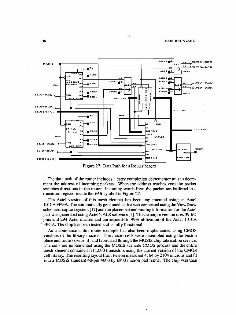
Figure 27: Data Path for a Router Macro
The data path of the router includes a carry completion decrementer unit to decrement the address of incoming packets. When the address reaches zero the packet switches directions in the router. Incoming words from the packet are buffered in a transition register inside the VAR symbol in Figure 27.
The Actel version of this mesh element has been implemented using an Actel 1010AFPGA. The automatically generated netlist was connected using the ViewDraw schematic capture system [17] and the placement and routing information for the Actel part was generated using Actel’s ALS software [1]. This example version uses 39 I/O pins and 294 Actel macros and corresponds to 99% utilization of the Actel 1010A
' FPGA. The chip has been tested and is fully functional.As a comparison, this router example has also been implemented using CMOS
versions of the library macros. The macro cells were assembled using the Fusion place and route service [3] and fabricated through the MOSIS chip fabrication service. The cells are implemented using the MOSIS scalable CMOS process and the entire mesh element contained «11,000 transistors using the current version of the CMOS cell library. The resulting layout from Fusion measured 4164 by 2104 microns and fit into a MOSIS standard 40-pin 4600 by 6800 micron pad frame. The chip was then
• REQ■ACK
•REQ
■ACK

A CELL SET FOR SELF-TIMED DESIGN USING ACTEL FPGAS 31
fabricated through MOSIS and tested. Unfortunately, due to a design rule violation in the Fusion-provided routing, the chip was not fully functional. Luckily, the design rule violation resulted only in the inadvertent connection of three data path wires from different parts of the circuit so although the data path was not correct, the control path ■ could be tested and was found to be fully functional.
5 Conclusions .
Although asynchronous and self-timed circuits can offer significant advantages over their synchronous counterparts, they are not widely used at present. Given the lack of experience with this form of circuit and system design, it is especially important that designers are able to try out a variety of designs quickly and inexpensively before committing to the final design. One stumbling block is the lack of suitable commercial circuits. This problem can be overcome by designing the needed parts directly in custom VLSI. However, the cost of custom VLSI implementations and the turnaround time for fabrication of parts conspire to make custom VLSI an expensive choice for experimenting with novel system designs. Field programmable gate arrays are an excellent alternative for fast inexpensive system prototyping provided the necessary circuit primitives can be implemented.
This report has presented a macro library that allows self-timed circuits and systems to be implemented using Actel field programmable gate arrays. The small size of the Actel basic macro makes it an ideal choice for implementing novel circuit structures beyond what the Actel designers envisioned. The self-timed macros are implemented in a small number of Actel basic modules and have been tested for functionality. A number of example designs have been built using the macro library, including student projects from a graduate seminar on asynchronous circuit design at the University of Utah. These macros have also been implemented as a CMOS cell set compatible with the MOSIS integrated circuit fabrication service. This allows designs prototyped using Actel FPGAs to be implemented in CMOS if desired after testing is complete.
In addition to being an excellent way to quickly implement and evaluate research ideas, this Actel macro library is also an excellent teaching tool. Students can learn the basics of self-timed circuit design, design a small project, and implement and test that circuit all in the same quarter. The Actel FPGA allows the peculiar circuits required
. for self-timed design to be implemented easily, and allows instant implementation of a finished design.
The main drawbacks to asynchronous design using Actel FPGAs are the inability to build more exotic Arbiter circuits, lack of control over signal routing which can make the bundling constraint harder to guarantee, and the size of the Actel part itself. One drawback to asynchronous and self-timed design in general is the extra circuitry needed to implement completion signals. While FPGAs are growing in capacity, current generation parts still always seem to have not quite enough logic modules for the task at hand.

32 ERIK BRUNVAND
Many thanks to the students in my CS572 VLSI Architecture class for helping to work the bugs out of this library, and to Nick Michell for additional testing and the. design of the carry completion adder macro.
References ,
1. Actel Corporation. ACT Family Field Programmable Gate Array Databook, March 1991.
2. T.S. Anantharaman. A delay insensitive regular expression recognizer. Technical report, Carnegie Mellon University, Mar 1986.
3. Ronald F. Ayres. Fusion: A new mosis service. Technical Report IS1/TM-87-194, Information Sciences Institute, 1987.
4. Erik Brunvand. Parts-R-Us: A chip aparts ... Technical Report CMU-CS-87-119, Carnegie Mellon University, 1987.
5. Erik Brunvand. Translating Concurrent Communicating Programs into Asynchronous Circuits. PhD thesis, Carnegie Mellon University, 1991.
6. Erik Brunvand and Robert F. Sproull. Translating concurrent programs into delay-insensitive circuits. In ICCAD-89, pages 262-265. IEEE, November 1989.
7. William J. Dally and Charles L. Seitz. The torus routing chip. Distributed Computing, 1:187-196,1986.
8. liana David, Ran Ginosar, and Michael Yoeli. An efficient implementation of boolean functions as self-timed circuits. Technical report, Technion, 1989.
9. Abbas El Gamal, Jonathan Greene, Justin Reyneri, Eric Rogoyski, Khaled A. El- Ayat, and Amr Mohsen. An architecture for electrically configurable gate arrays. IEEE Journal o f Solid State Circuits, 24(2), April 1989.
10. Kai Hwang. Computer Arithmetic: Principles, Architecture, and Design. John ' Wiley & Sons, Inc., 1979.
11. Inmos. Occam Programming Manual, 1983.
12. Fred U. Rosenbeiger, Charles E. Molnar, Thomas J. Chaney, and Ting-Pien Fang. Q-modules: internally clocked delay-insensitive modules. IEEE Transactions on Computers, 37(9), Sept 1988.
13. C. L. Seitz. System timing. In Mead and Conway, Introduction to VLSI Systems, chapter 7. Addison-Wesley, 1980.
6 Acknowledgments

14. N. P. Singh. A design methodology for self-timed systems. Master’s thesis, MIT,1981.
15. Ivan Sutherland. Micropipelines. CACM, 32(6), 1989.
16. Ivan E. Sutherland, Robert F. Sproull, and Ian Jones. Standard asynchronous modules. Technical Memo 4662, Sutherland, Sproull and Associates, 1986.
17. ViewLogic Corporation. Workview Reference Manual, 1991. •
A CELL SET FOR SELF-TIMED DESIGN USING ACTEL FPGAS 33