act 2 family fpgas - obspm.frpccorot15.obspm.fr/corot-etc/files/actel act2 serie.pdf · act ™ 2...
TRANSCRIPT

April 1996
1-169
© 1996 Actel Corporation
AC
T2
1
ACT
™
2 Family FPGAs
Features
• Up to 8000 Gate Array Gates (20,000 PLD equivalent gates)
• Replaces up to 200 TTL Packages
• Replaces up to eighty 20-Pin PAL
®
Packages
• Design Library with over 500 Macro Functions
• Single-Module Sequential Functions
• Wide-Input Combinatorial Functions
• Up to 1232 Programmable Logic Modules
• Up to 998 Flip-Flops
• Datapath Performance at 105 MHz
• 16-Bit Accumulator Performance to 39 MHz
• Two In-Circuit Diagnostic Probe Pins Support SpeedAnalysis to 50 MHz
• Two High-Speed, Low-Skew Clock Networks
• I/O Drive to 10 mA
• Nonvolatile, User Programmable
• Logic Fully Tested Prior to Shipment
• 1.0-micron CMOS Technology
Product Family Profile
Device A1225A A1240A A1280A
CapacityGate Array Equivalent GatesPLD Equivalent GatesTTL Equivalent Packages20-Pin PAL Equivalent Packages
2,5006,250
6325
4,00010,000
10040
8,00020,000
20080
Logic ModulesS-ModulesC-Modules
451231220
684348336
1,232624608
Flip-Flops (maximum) 382 568 998
Routing ResourcesHorizontal Tracks/ChannelVertical Tracks/ChannelPLICE Antifuse Elements
3615
250,000
3615
400,000
3615
750,000
User I/Os (maximum) 83 104 140
Packages
1
100 CPGA100 PQFP100 VQFP
84 PLCC
132 CPGA144 PQFP176 TQFP84 PLCC
176 CPGA160 PQFP176 TQFP84 PLCC
172 CQFP
Performance
2
16-Bit Prescaled Counters16-Bit Loadable Counters16-Bit Accumulators
105 MHz70 MHz39 MHz
100 MHz69 MHz38 MHz
85 MHz67 MHz36 MHz
Notes:
1. See product plan on page 1-171 for package availability.2. Performance is based on ‘–2’ speed devices at commercial worst-case operating conditions using PREP Benchmarks, Suite #1, Version 1.2,
dated 3-28-93, any analysis is not endorsed by PREP.

1-170
Description
The ACT™ 2 family represents Actel’s second generation offield programmable gate arrays (FPGAs). The ACT 2 familypresents a two-module architecture, consisting of C-modulesand S-modules. These modules are optimized for bothcombinatorial and sequential designs. Based on Actel’spatented channeled array architecture, the ACT 2 familyprovides significant enhancements to gate density andperformance while maintaining downward compatibility withthe ACT 1 design environment and upward compatibility withthe ACT 3 design environment. The devices are implementedin silicon gate, 1.0-
µ
m, two-level metal CMOS, and employ
Actel’s PLICE
®
antifuse technology. This revolutionaryarchitecture offers gate array design flexibility, highperformance, and fast time-to-production with userprogramming. The ACT 2 family is supported by the Designerand Designer Advantage Systems, which offers automatic pinassignment, validation of electrical and design rules,automatic placement and routing, timing analysis, userprogramming, and diagnostic probe capabilities. The systemsare supported on the following platforms: 386/486™ PC,Sun
™
, and HP
™
workstations. The systems provide CAEinterfaces to the following design environments: Cadence,Viewlogic
®
, Mentor Graphics
®
, and OrCAD™.
Ordering Information
Application (Temperature Range)C = Commercial (0 to +70°C)I = Industrial (–40 to +85°C)M = Military (–55 to +125°C)B = MIL-STD-883
Package TypePL = Plastic J-Leaded Chip CarrierPQ = Plastic Quad FlatpackCQ = Ceramic Quad FlatpackPG = Ceramic Pin Grid ArrayTQ = Thin (1.4 mm) Quad FlatpackVQ = Very Thin (1.0 mm) Quad Flatpack
Speed GradeBlank = Standard Speed
–1 = Approximately 15% faster than Standard–2 = Approximately 25% faster than Standard
Part NumberA1225 = 2500 GatesA1240 = 4000 GatesA1280 = 8000 Gates
Die RevisionA = 1.0-µm CMOS process
Package Lead Count
A1280 – PG 176 C1A

1-171
ACT
™
2 Family FPGAs
AC
T2
1
Product Plan
1
Device Resources
Speed Grade* Application
Std –1 –2 C I M B
A1225A Device
100-pin Ceramic Pin Grid Array (PG)
100-pin Plastic Quad Flatpack (PQ)100-pin Very Thin (1.0 mm) Quad Flatpack (VQ)
84-pin Plastic Leaded Chip Carrier (PL)
—
—
—
—
——
—
—
——
A1240A Device
132-pin Ceramic Pin Grid Array (PG)176-pin Thin (1.4 mm) Quad Flatpack (TQ)
144-pin Plastic Quad Flatpack (PQ)
84-pin Plastic Leaded Chip Carrier (PL)
——
——
—
—
——
A1280A Device
176-pin Ceramic Pin Grid Array (PG)176-pin Thin (1.4 mm) Quad Flatpack (TQ)
160-pin Plastic Quad Flatpack (PQ)
172-pin Ceramic Quad Flatpack (CQ)
——
—
——
——
Applications: C = Commercial Availability:
= Available * Speed Grade: –1 = Approx. 15% faster than StandardI = Industrial P = Planned –2 = Approx. 25% faster than StandardM = Military — = Not PlannedB = MIL-STD-883
Note:
1. Please consult Actel representatives for current availability.
User I/Os
Device Series
Logic Modules Gates
CPGA PQFP PLCC CQFP TQFP VQFP
176-pin 132-pin 100-pin 160-pin 144-pin 100-pin 84-pin 172-pin 176-pin 100-pin
A1225A 451 2500 — — 83 — — 83 72 — — 83
A1240A 684 4000 — 104 — — 104 — 72 — 104 —
A1280A 1232 8000 140 — — 125 — — 72 140 140 —
1-172
Pin Description
CLKA Clock A (Input)
TTL Clock input for clock distribution networks. The Clockinput is buffered prior to clocking the logic modules. This pincan also be used as an I/O.
CLKB Clock B (Input)
TTL Clock input for clock distribution networks. The Clockinput is buffered prior to clocking the logic modules. This pincan also be used as an I/O.
DCLK Diagnostic Clock (Input)
TTL Clock input for diagnostic probe and deviceprogramming. DCLK is active when the MODE pin is HIGH.This pin functions as an I/O when the MODE pin is LOW.
GND Ground
LOW supply voltage.
I/O Input/Output (Input, Output)
The I/O pin functions as an input, output, three-state, orbidirectional buffer. Input and output levels are compatiblewith standard TTL and CMOS specifications. Unused I/O pinsare automatically driven LOW by the ALS software.
MODE Mode (Input)
The MODE pin controls the use of multifunction pins (DCLK,PRA, PRB, SDI). When the MODE pin is HIGH, the specialfunctions are active. When the MODE pin is LOW, the pinsfunction as I/Os. To provide Actionprobe capability, theMODE pin should be terminated to GND through a 10Kresistor so that the MODE pin can be pulled high whenrequired.
NC No Connection
This pin is not connected to circuitry within the device.
PRA Probe A (Output)
The Probe A pin is used to output data from any user-defineddesign node within the device. This independent diagnosticpin is used in conjunction with the Probe B pin to allowreal-time diagnostic output of any signal path within thedevice. The Probe A pin can be used as a user-defined I/Owhen debugging has been completed. The pin’s probecapabilities can be permanently disabled to protectprogrammed design confidentiality. PRA is active when theMODE pin is HIGH. This pin functions as an I/O when theMODE pin is LOW.
PRB Probe B (Output)
The Probe B pin is used to output data from any user-defineddesign node within the device. This independent diagnosticpin is used in conjunction with the Probe A pin to allowreal-time diagnostic output of any signal path within thedevice. The Probe B pin can be used as a user-defined I/Owhen debugging has been completed. The pin’s probecapabilities can be permanently disabled to protectprogrammed design confidentiality. PRB is active when theMODE pin is HIGH. This pin functions as an I/O when theMODE pin is LOW.
SDI Serial Data Input (Input)
Serial data input for diagnostic probe and deviceprogramming. SDI is active when the MODE pin is HIGH. Thispin functions as an I/O when the MODE pin is LOW.
V
CC
5 V Supply Voltage
HIGH supply voltage.

1-173
ACT
™
2 Family FPGAs
AC
T2
1
Absolute Maximum Ratings
1
Free air temperature range
Recommended Operating Conditions
Electrical Specifications
Symbol Parameter Limits Units
V
CC
DC Supply Voltage –0.5 to +7.0 V
V
I
Input Voltage –0.5 to V
CC
+0.5 V
V
O
Output Voltage –0.5 to V
CC
+0.5 V
I
IO
I/O Source/SinkCurrent
2
±
20 mA
T
STG
Storage Temperature –65 to +150
°
C
Notes:
1. Stresses beyond those listed under “Absolute MaximumRatings” may cause permanent damage to the device. Exposureto absolute maximum rated conditions for extended periodsmay affect device reliability. Device should not be operatedoutside the Recommended Operating Conditions.
2. Device inputs are normally high impedance and drawextremely low current. However, when input voltage is greaterthan V
CC
+ 0.5 V or less than GND – 0.5 V, the internalprotection diode will be forward biased and can draw excessivecurrent.
Parameter Commercial Industrial Military Units
Temperature Range
1
0 to +70 –40 to +85
–55 to +125
°
C
Power Supply Tolerance
±
5
±
10
±
10 %V
CC
Notes:
1. Ambient temperature (T
A
) is used for commercial andindustrial; case temperature (T
C
) is used for military.
Symbol Parameter
Commercial Industrial Military
UnitsMin. Max. Min. Max. Min. Max.
V
OH1
(I
OH
= –10 mA)
2
2.4 V
(I
OH
= –6 mA) 3.84 V
(I
OH
= –4 mA) 3.7 3.7 V
V
OL1
(I
OL
= 10 mA)
2
0.5 V
(I
OL
= 6 mA) 0.33 0.40 0.40 V
V
IL
–0.3 0.8 –0.3 0.8 –0.3 0.8 V
V
IH
2.0 V
CC
+ 0.3 2.0 V
CC
+ 0.3 2.0 V
CC
+ 0.3 V
Input Transition Time t
R
, t
F2
500 500 500 ns
C
IO
I/O Capacitance
2, 3
10 10 10 pF
Standby Current, I
CC4
(typical = 1 mA) 2 10 20 mA
Leakage Current
5
–10 10 –10 10 –10 10
µ
A
Notes:
1. Only one output tested at a time. V
CC
= min.2. Not tested, for information only.3. Includes worst-case 176 CPGA package capacitance. V
OUT
= 0 V, f = 1 MHz.4. All outputs unloaded. All inputs = V
CC
or GND, typical I
CC
= 1 mA. I
CC
limit includes I
PP
and I
SV
during normal operation.5. V
OUT
, V
IN
= V
CC
or GND.

1-174
Package Thermal Characteristics
The device junction to case thermal characteristic is
θ
jc, andthe junction to ambient air characteristic is
θ
ja. The thermalcharacteristics for
θ
ja are shown with two different air flowrates.
Maximum junction temperature is 150
°
C.
A sample calculation of the absolute maximum powerdissipation allowed for a PQFP 160-pin package atcommercial temperature is as follows:
Power Dissipation
P = [I
CC
standby + ICCactive] * VCC + IOL * VOL * N + IOH * (VCC – VOH) * M
Where:
ICC standby is the current flowing when no inputs oroutputs are changing.
ICC active is the current flowing due to CMOS switching.
IOL, IOH are TTL sink/source currents.
VOL, VOH are TTL level output voltages.
N equals the number of outputs driving TTL loads to VOL.
M equals the number of outputs driving TTL loads to VOH.
An accurate determination of N and M is problematicalbecause their values depend on the family type, designdetails, and on the system I/O. The power can be divided intotwo components: static and active.
Static Power Component
Actel FPGAs have small static power components that resultin lower power dissipation than PALs or PLDs. By integratingmultiple PALs/PLDs into one FPGA, an even greaterreduction in board-level power dissipation can be achieved.
The power due to standby current is typically a smallcomponent of the overall power. Standby power is calculatedbelow for commercial, worst case conditions.
ICC VCC Power
2 mA 5.25 V 10.5 mW
The static power dissipated by TTL loads depends on thenumber of outputs driving high or low and the DC loadcurrent. Again, this value is typically small. For instance, a32-bit bus sinking 4 mA at 0.33 V will generate 42 mW with alloutputs driving low, and 140 mW with all outputs driving high.The actual dissipation will average somewhere between asI/Os switch states with time.
Active Power Component
Power dissipation in CMOS devices is usually dominated bythe active (dynamic) power dissipation. This component isfrequency dependent, a function of the logic and the externalI/O. Active power dissipation results from charging internalchip capacitances of the interconnect, unprogrammedantifuses, module inputs, and module outputs, plus externalcapacitance due to PC board traces and load device inputs.An additional component of the active power dissipation isthe totem-pole current in CMOS transistor pairs. The net
Package Type Pin Count θjcθja
Still Airθja
300 ft/min Units
Ceramic Pin Grid Array 100132176
558
353023
171512
°C/W°C/W°C/W
Ceramic Quad Flatpack 172 8 25 15 °C/W
Plastic Quad Flatpack1 100144160
131515
484038
403230
°C/W°C/W°C/W
Plastic Leaded Chip Carrier2 84 12 37 28 °C/W
Very Thin Quad Flatpack3 100 12 43 35 °C/W
Thin Quad Flatpack4 176 15 32 25 °C/W
Notes: (Maximum Power in Still Air)1. Maximum Power Dissipation for PQFP packages are 1.9 Watts (100-pin), 2.3 Watts (144-pin), and 2.4 Watts (160-pin).2. Maximum Power Dissipation for PLCC packages is 2.7 Watts.3. Maximum Power Dissipation for VQFP packages is 2.3 Watts.4. Maximum Power Dissipation for TQFP packages is 3.1 Watts.
Max. junction temp. ( ° C) – Max. commercial temp. θ
ja ( ° C/W)
----------------------------------------------------------------------------------------------------------------------------- 150
°
C – 70 ° C33
°
C/W
--------------------------------- 2.4 W= =
1-175
ACT
™
2 Family FPGAs
AC
T2
1
effect can be associated with an equivalent capacitance thatcan be combined with frequency and voltage to representactive power dissipation.
Equivalent Capacitance
The power dissipated by a CMOS circuit can be expressed bythe Equation 1.
Power (uW) = C EQ
* V CC
2 * F (1)
Where:
C
EQ
is the equivalent capacitance expressed in pF.
V
CC
is the power supply in volts.
F is the switching frequency in MHz.
Equivalent capacitance is calculated by measuring ICC activeat a specified frequency and voltage for each circuitcomponent of interest. Measurements have been made over arange of frequencies at a fixed value of VCC. Equivalentcapacitance is frequency independent so that the results maybe used over a wide range of operating conditions. Equivalentcapacitance values are shown below.
C
EQ
Values for Actel FPGAs
Modules (C
EQM
) 5.8
Input Buffers (C
EQI
) 12.9
Output Buffers (C
EQO
) 23.8
Routed Array Clock Buffer Loads (C
EQCR
) 3.9
To calculate the active power dissipated from the completedesign, the switching frequency of each part of the logic mustbe known. Equation 2 shows a piece-wise linear summationover all components.
Power = V
CC2
* [(m * C
EQM
* f
m
)
modules
+(n * C
EQI
* f
n
)
inputs
+ (p * (C
EQO
+ C
L
) * f
p
)
outputs
+ 0.5 * (q
1
* C
EQCR
* f
q1
)
routed_Clk1
+ (r
1
* f
q1
)
routed_Clk1
+ 0.5 * (q
2
* C
EQCR
* f
q2
)
routed_Clk2
+ (r
2
* f
q2
)
routed_Clk2
] (2)
Where:
Fixed Capacitance Values for Actel FPGAs (pF)
r1 r2Device Type routed_Clk1 routed_Clk2
A1225A 106 106.0A1240A 134 134.2A1280A 168 167.8
Determining Average Switching Frequency
To determine the switching frequency for a design, you musthave a detailed understanding of the data input values to thecircuit. The following guidelines are meant to representworst-case scenarios so that they can be generally used topredict the upper limits of power dissipation. Theseguidelines are as follows:
m = Number of logic modules switching at fm
n = Number of input buffers switching at fn
p = Number of output buffers switching at fp
q1 = Number of clock loads on the first routed arrayclock
q2 = Number of clock loads on the second routed arrayclock
r1 = Fixed capacitance due to first routed array clock
r2 = Fixed capacitance due to second routed arrayclock
CEQM = Equivalent capacitance of logic modules in pF
CEQI = Equivalent capacitance of input buffers in pF
CEQO = Equivalent capacitance of output buffers in pF
CEQCR = Equivalent capacitance of routed array clock inpF
CL = Output lead capacitance in pF
fm = Average logic module switching rate in MHz
fn = Average input buffer switching rate in MHz
fp = Average output buffer switching rate in MHz
fq1 = Average first routed array clock rate in MHz
fq2 = Average second routed array clock rate in MHz
Logic Modules (m) 80% of modules
Inputs switching (n) # inputs/4
Outputs switching (p) # outputs/4
First routed array clock loads (q1) 40% of sequential modules
Second routed array clock loads (q2) 40% of sequential modules
Load capacitance (CL) 35 pF
Average logic module switching rate (fm) F/10
Average input switching rate (fn) F/5
Average output switching rate (fp) F/10
Average first routed array clock rate (fq1) F
Average second routed array clock rate(fq2)
F/2

1-176
ACT 2 Timing Model*
*Values shown for A1240A-2 at worst-case commercial conditions. † Input Module Predicted Routing Delay
Output DelaysInternal DelaysInput Delays
tINH = 2.0 nstINSU = 4.0 ns
I/O Module
D Q
tINGL = 4.7 ns
tINYL = 2.6 ns tIRD2 = 4.8 ns†
CombinatorialLogic Module
tPD = 3.8 ns
SequentialLogic Module
I/O Module
tRD1 = 1.4 nstDLH = 8.0 ns
I/O Module
ARRAYCLOCKS
FMAX = 100 MHz
Combin-atorial Logicincluded in tSUD
D Q D Q
tOUTH = 0.0 nstOUTSU = 0.4 ns
tGLH = 9.0 ns
tDLH = 8.0 ns
tENHZ = 7.1 nstRD1 = 1.4 ns
tCO = 3.8 nstSUD = 0.4 nstHD = 0.0 ns
tRD4 = 3.1 nstRD8 = 4.7 ns
PredictedRoutingDelays
tCKH = 11.8 ns
G
G
FO = 256
tRD2 = 1.7 ns
1-177
ACT™ 2 Family FPGAs
AC
T2
1
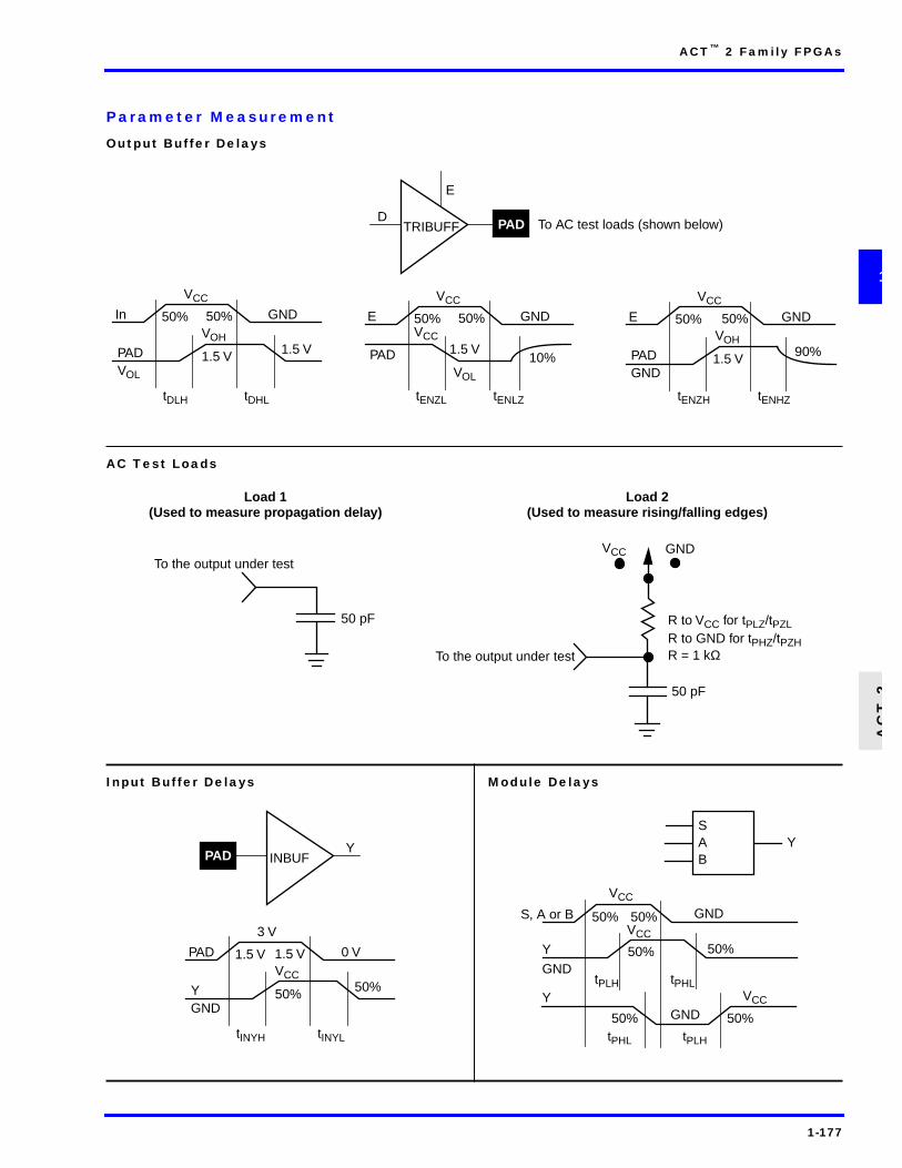
Parameter Measurement
Output Buffer Delays
AC Test Loads
Input Buffer Delays Module Delays
To AC test loads (shown below)D
E
TRIBUFF
In
VCC
GND50%
PADVOL
VOH
1.5 V
tDLH
50%
1.5 V
tDHL
E
VCC
GND50%
PADVOL
1.5 V
tENZL
50%
10%
tENLZ
E
VCC
GND50%
PADGND
VOH
1.5 V
tENZH
50%
90%
tENHZ
VCC
PAD
Load 1(Used to measure propagation delay)
Load 2(Used to measure rising/falling edges)
50 pF
To the output under testVCC GND
50 pF
To the output under test
R to VCC for tPLZ/tPZLR to GND for tPHZ/tPZHR = 1 kΩ
YINBUF
PAD
3 V
0 V1.5 V
YGND
VCC
50%
tINYH
1.5 V
50%
tINYL
PAD
SAB
Y
S, A or B
Y
GND
VCC
50%
tPLH
Y
GND
GND
VCC
50%
50% 50%
VCC
50% 50%tPHL
tPHLtPLH

1-178
Sequential Module Timing Characteristics
Flip-Flops and Latches
Note: D represents all data functions involving A, B, and S for multiplexed flip-flops.
(Positive edge triggered)
DE
CLK CLR
PRE Y
D1
G, CLK
E
Q
PRE, CLR
tWCLKA
tWASYN
tHD
tSUENA
tSUD
tRS
tA
tWCLKI
tCO
tHENA

1-179
ACT™ 2 Family FPGAs
AC
T2
1
Sequential Timing Characteristics (continued)
Input Buffer Latches
Output Buffer Latches
G
PAD
PADCLK
DATA
G
CLK
tINH
CLKBUF
tINSU
tSUEXT
tHEXT
IBDLDATA
D
G
tOUTSU
tOUTH
PAD
OBDLHS
D
G

1-180
Timing Derating Factor (Temperature and Voltage)
Timing Derating Factor for Designs at Typical Temperature (TJ = 25°C) and Voltage (5.0 V)
Temperature and Voltage Derating Factors (normalized to Worst-Case Commercial, TJ = 4.75 V, 70°C)
Industrial Military
Min. Max. Min. Max.
(Commercial Minimum/Maximum Specification) x 0.69 1.11 0.67 1.23
(Commercial Maximum Specification) x 0.85
–55 –40 0 25 70 85 125
4.50 0.75 0.79 0.86 0.92 1.06 1.11 1.23
4.75 0.71 0.75 0.82 0.87 1.00 1.05 1.16
5.00 0.69 0.72 0.80 0.85 0.97 1.02 1.13
5.25 0.68 0.69 0.77 0.82 0.95 0.98 1.09
5.50 0.67 0.69 0.76 0.81 0.93 0.97 1.08
Note: This derating factor applies to all routing and propagation delays.
0.6
0.7
0.8
0.9
1.0
1.1
1.2
1.3
4.50 4.75 5.00 5.25 5.50
Der
atin
g F
acto
r
Voltage (V)
125°C
85°C70°C
25°C
0°C
–40°C–55°C
Junction Temperature and Voltage Derating Curves (normalized to Worst-Case Commercial, TJ = 4.75 V, 70°C)

1-181
ACT™ 2 Family FPGAs
AC
T2
1
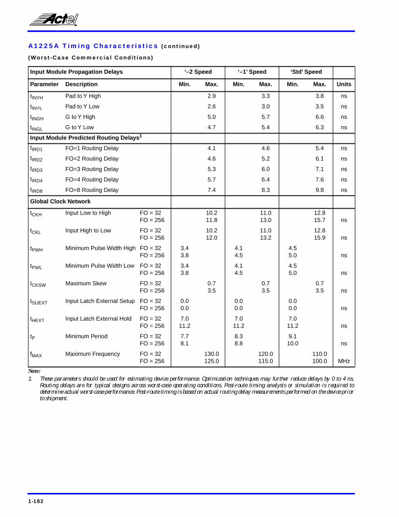
A1225A Timing Characteristics
(Worst-Case Commercial Conditions, VCC = 4.75 V, TJ = 70°C)
Notes:1. For dual-module macros, use tPD1 + tRD1 + tPDn , tCO + tRD1 + tPDn or tPD1 + tRD1 + tSUD, whichever is appropriate.2. Routing delays are for typical designs across worst-case operating conditions. These parameters should be used for estimating device
performance. Post-route timing analysis or simulation is required to determine actual worst-case performance. Post-route timing is basedon actual routing delay measurements performed on the device prior to shipment.
3. Data applies to macros based on the S-module. Timing parameters for sequential macros constructed from C-modules can be obtained fromthe DirectTime Analyzer utility.
4. Setup and hold timing parameters for the Input Buffer Latch are defined with respect to the PAD and the D input. External setup/hold timingparameters must account for delay from an external PAD signal to the G inputs. Delay from an external PAD signal to the G input subtracts(adds) to the internal setup (hold) time.
Logic Module Propagation Delays1 ‘–2’ Speed ‘–1’ Speed ‘Std’ Speed
Parameter Description Min. Max. Min. Max. Min. Max. Units
tPD1 Single Module 3.8 4.3 5.0 ns
tCO Sequential Clk to Q 3.8 4.3 5.0 ns
tGO Latch G to Q 3.8 4.3 5.0 ns
tRS Flip-Flop (Latch) Reset to Q 3.8 4.3 5.0 ns
Predicted Routing Delays2
tRD1 FO=1 Routing Delay 1.1 1.2 1.4 ns
tRD2 FO=2 Routing Delay 1.7 1.9 2.2 ns
tRD3 FO=3 Routing Delay 2.3 2.6 3.0 ns
tRD4 FO=4 Routing Delay 2.8 3.1 3.7 ns
tRD8 FO=8 Routing Delay 4.4 4.9 5.8 ns
Sequential Timing Characteristics3,4
tSUD Flip-Flop (Latch) Data Input Setup 0.4 0.4 0.5 ns
tHD Flip-Flop (Latch) Data Input Hold 0.0 0.0 0.0 ns
tSUENA Flip-Flop (Latch) Enable Setup 0.8 0.9 1.0 ns
tHENA Flip-Flop (Latch) Enable Hold 0.0 0.0 0.0 ns
tWCLKA Flip-Flop (Latch) Clock Active Pulse Width 4.5 5.0 6.0 ns
tWASYN Flip-Flop (Latch) Asynchronous Pulse Width 4.5 5.0 6.0 ns
tA Flip-Flop Clock Input Period 9.4 11.0 13.0 ns
tINH Input Buffer Latch Hold 0.0 0.0 0.0 ns
tINSU Input Buffer Latch Setup 0.4 0.4 0.5 ns
tOUTH Output Buffer Latch Hold 0.0 0.0 0.0 ns
tOUTSU Output Buffer Latch Setup 0.4 0.4 0.5 ns
fMAX Flip-Flop (Latch) Clock Frequency 105.0 90.0 75.0 MHz
1-182
A1225A Timing Characteristics (continued)
(Worst-Case Commercial Conditions)
Note:1. These parameters should be used for estimating device performance. Optimization techniques may further reduce delays by 0 to 4 ns.
Routing delays are for typical designs across worst-case operating conditions. Post-route timing analysis or simulation is required todetermine actual worst-case performance. Post-route timing is based on actual routing delay measurements performed on the device priorto shipment.
Input Module Propagation Delays ‘–2 Speed ‘–1’ Speed ‘Std’ Speed
Parameter Description Min. Max. Min. Max. Min. Max. Units
tINYH Pad to Y High 2.9 3.3 3.8 ns
tINYL Pad to Y Low 2.6 3.0 3.5 ns
tINGH G to Y High 5.0 5.7 6.6 ns
tINGL G to Y Low 4.7 5.4 6.3 ns
Input Module Predicted Routing Delays1
tIRD1 FO=1 Routing Delay 4.1 4.6 5.4 ns
tIRD2 FO=2 Routing Delay 4.6 5.2 6.1 ns
tIRD3 FO=3 Routing Delay 5.3 6.0 7.1 ns
tIRD4 FO=4 Routing Delay 5.7 6.4 7.6 ns
tIRD8 FO=8 Routing Delay 7.4 8.3 9.8 ns
Global Clock Network
tCKH Input Low to High FO = 32FO = 256
10.211.8
11.013.0
12.815.7 ns
tCKL Input High to Low FO = 32FO = 256
10.212.0
11.013.2
12.815.9 ns
tPWH Minimum Pulse Width High FO = 32FO = 256
3.43.8
4.14.5
4.55.0 ns
tPWL Minimum Pulse Width Low FO = 32FO = 256
3.43.8
4.14.5
4.55.0 ns
tCKSW Maximum Skew FO = 32FO = 256
0.73.5
0.73.5
0.73.5 ns
tSUEXT Input Latch External Setup FO = 32FO = 256
0.00.0
0.00.0
0.00.0 ns
tHEXT Input Latch External Hold FO = 32FO = 256
7.011.2
7.011.2
7.011.2 ns
tP Minimum Period FO = 32FO = 256
7.78.1
8.38.8
9.110.0 ns
fMAX Maximum Frequency FO = 32FO = 256
130.0125.0
120.0115.0
110.0100.0 MHz

1-183
ACT™ 2 Family FPGAs
AC
T2
1
A1225A Timing Characteristics (continued)
(Worst-Case Commercial Conditions)
Notes:1. Delays based on 50 pF loading.2. SSO information can be found in the “Simultaneous Switching Output Limits for Actel FPGAs” application note on page 4-125.
Output Module Timing ‘–2 Speed ‘–1’ Speed ‘Std’ Speed
Parameter Description Min. Max. Min. Max. Min. Max. Units
TTL Output Module Timing1, 2
tDLH Data to Pad High 8.0 9.0 10.6 ns
tDHL Data to Pad Low 10.1 11.4 13.4 ns
tENZH Enable Pad Z to High 8.9 10.0 11.8 ns
tENZL Enable Pad Z to Low 11.6 13.2 15.5 ns
tENHZ Enable Pad High to Z 7.1 8.0 9.4 ns
tENLZ Enable Pad Low to Z 8.3 9.5 11.1 ns
tGLH G to Pad High 8.9 10.2 11.9 ns
tGHL G to Pad Low 11.2 12.7 14.9 ns
dTLH Delta Low to High 0.07 0.08 0.09 ns/pF
dTHL Delta High to Low 0.12 0.13 0.16 ns/pF
CMOS Output Module Timing1, 2
tDLH Data to Pad High 10.1 11.5 13.5 ns
tDHL Data to Pad Low 8.4 9.6 11.2 ns
tENZH Enable Pad Z to High 8.9 10.0 11.8 ns
tENZL Enable Pad Z to Low 11.6 13.2 15.5 ns
tENHZ Enable Pad High to Z 7.1 8.0 9.4 ns
tENLZ Enable Pad Low to Z 8.3 9.5 11.1 ns
tGLH G to Pad High 8.9 10.2 11.9 ns
tGHL G to Pad Low 11.2 12.7 14.9 ns
dTLH Delta Low to High 0.12 0.13 0.16 ns/pF
dTHL Delta High to Low 0.09 0.10 0.12 ns/pF

1-184
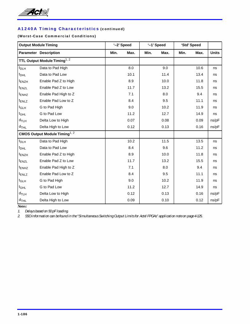
A1240A Timing Characteristics
(Worst-Case Commercial Conditions, VCC = 4.75 V, TJ = 70°C)
Notes:1. For dual-module macros, use tPD1 + tRD1 + tPDn , tCO + tRD1 + tPDn or tPD1 + tRD1 + tSUD, whichever is appropriate.2. Routing delays are for typical designs across worst-case operating conditions. These parameters should be used for estimating device
performance. Post-route timing analysis or simulation is required to determine actual worst-case performance. Post-route timing is basedon actual routing delay measurements performed on the device prior to shipment.
3. Data applies to macros based on the S-module. Timing parameters for sequential macros constructed from C-modules can be obtained fromthe DirectTime Analyzer utility.
4. Setup and hold timing parameters for the Input Buffer Latch are defined with respect to the PAD and the D input. External setup/hold timingparameters must account for delay from an external PAD signal to the G inputs. Delay from an external PAD signal to the G input subtracts(adds) to the internal setup (hold) time.
Logic Module Propagation Delays1 ‘–2’ Speed ‘–1’ Speed ‘Std’ Speed
Parameter Description Min. Max. Min. Max. Min. Max. Units
tPD1 Single Module 3.8 4.3 5.0 ns
tCO Sequential Clk to Q 3.8 4.3 5.0 ns
tGO Latch G to Q 3.8 4.3 5.0 ns
tRS Flip-Flop (Latch) Reset to Q 3.8 4.3 5.0 ns
Predicted Routing Delays2
tRD1 FO=1 Routing Delay 1.4 1.5 1.8 ns
tRD2 FO=2 Routing Delay 1.7 2.0 2.3 ns
tRD3 FO=3 Routing Delay 2.3 2.6 3.0 ns
tRD4 FO=4 Routing Delay 3.1 3.5 4.1 ns
tRD8 FO=8 Routing Delay 4.7 5.4 6.3 ns
Sequential Timing Characteristics3, 4
tSUD Flip-Flop (Latch) Data Input Setup 0.4 0.4 0.5 ns
tHD Flip-Flop (Latch) Data Input Hold 0.0 0.0 0.0 ns
tSUENA Flip-Flop (Latch) Enable Setup 0.8 0.9 1.0 ns
tHENA Flip-Flop (Latch) Enable Hold 0.0 0.0 0.0 ns
tWCLKA Flip-Flop (Latch) Clock Active Pulse Width 4.5 6.0 6.5 ns
tWASYN Flip-Flop (Latch) Asynchronous Pulse Width 4.5 6.0 6.5 ns
tA Flip-Flop Clock Input Period 9.8 12.0 15.0 ns
tINH Input Buffer Latch Hold 0.0 0.0 0.0 ns
tINSU Input Buffer Latch Setup 0.4 0.4 0.5 ns
tOUTH Output Buffer Latch Hold 0.0 0.0 0.0 ns
tOUTSU Output Buffer Latch Setup 0.4 0.4 0.5 ns
fMAX Flip-Flop (Latch) Clock Frequency 100.0 80.0 66.0 MHz

1-185
ACT™ 2 Family FPGAs
AC
T2
1
A1240A Timing Characteristics (continued)
(Worst-Case Commercial Conditions)
Note:1. These parameters should be used for estimating device performance. Optimization techniques may further reduce delays by 0 to 4 ns. Routing
delays are for typical designs across worst-case operating conditions. Post-route timing analysis or simulation is required to determineactual worst-case performance. Post-route timing is based on actual routing delay measurements performed on the device prior to shipment.
Input Module Propagation Delays ‘–2’ Speed ‘–1’ Speed ‘Std’ Speed
Parameter Description Min. Max. Min. Max. Min. Max. Units
tINYH Pad to Y High 2.9 3.3 3.8 ns
tINYL Pad to Y Low 2.6 3.0 3.5 ns
tINGH G to Y High 5.0 5.7 6.6 ns
tINGL G to Y Low 4.7 5.4 6.3 ns
Input Module Predicted Routing Delays1
tIRD1 FO=1 Routing Delay 4.2 4.8 5.6 ns
tIRD2 FO=2 Routing Delay 4.8 5.4 6.4 ns
tIRD3 FO=3 Routing Delay 5.4 6.1 7.2 ns
tIRD4 FO=4 Routing Delay 5.9 6.7 7.9 ns
tIRD8 FO=8 Routing Delay 7.9 8.9 10.5 ns
Global Clock Network
tCKH Input Low to High FO = 32FO = 256
10.211.8
11.013.0
12.815.7 ns
tCKL Input High to Low FO = 32FO = 256
10.212.0
11.013.2
12.815.9 ns
tPWH Minimum Pulse Width High FO = 32FO = 256
3.84.1
4.55.0
5.55.8 ns
tPWL Minimum Pulse Width Low FO = 32FO = 256
3.84.1
4.55.0
5.55.8 ns
tCKSW Maximum Skew FO = 32FO = 256
0.52.5
0.52.5
0.52.5 ns
tSUEXT Input Latch External Setup FO = 32FO = 256
0.00.0
0.00.0
0.00.0 ns
tHEXT Input Latch External Hold FO = 32FO = 256
7.011.2
7.011.2
7.011.2 ns
tP Minimum Period FO = 32FO = 256
8.18.8
9.110.0
11.111.7 ns
fMAX Maximum Frequency FO = 32FO = 256
125.0115.0
110.0100.0
90.085.0 MHz
1-186
A1240A Timing Characteristics (continued)
(Worst-Case Commercial Conditions)
Notes:1. Delays based on 50 pF loading.2. SSO information can be found in the “Simultaneous Switching Output Limits for Actel FPGAs” application note on page 4-125.
Output Module Timing ‘–2’ Speed ‘–1’ Speed ‘Std’ Speed
Parameter Description Min. Max. Min. Max. Min. Max. Units
TTL Output Module Timing1, 2
tDLH Data to Pad High 8.0 9.0 10.6 ns
tDHL Data to Pad Low 10.1 11.4 13.4 ns
tENZH Enable Pad Z to High 8.9 10.0 11.8 ns
tENZL Enable Pad Z to Low 11.7 13.2 15.5 ns
tENHZ Enable Pad High to Z 7.1 8.0 9.4 ns
tENLZ Enable Pad Low to Z 8.4 9.5 11.1 ns
tGLH G to Pad High 9.0 10.2 11.9 ns
tGHL G to Pad Low 11.2 12.7 14.9 ns
dTLH Delta Low to High 0.07 0.08 0.09 ns/pF
dTHL Delta High to Low 0.12 0.13 0.16 ns/pF
CMOS Output Module Timing1, 2
tDLH Data to Pad High 10.2 11.5 13.5 ns
tDHL Data to Pad Low 8.4 9.6 11.2 ns
tENZH Enable Pad Z to High 8.9 10.0 11.8 ns
tENZL Enable Pad Z to Low 11.7 13.2 15.5 ns
tENHZ Enable Pad High to Z 7.1 8.0 9.4 ns
tENLZ Enable Pad Low to Z 8.4 9.5 11.1 ns
tGLH G to Pad High 9.0 10.2 11.9 ns
tGHL G to Pad Low 11.2 12.7 14.9 ns
dTLH Delta Low to High 0.12 0.13 0.16 ns/pF
dTHL Delta High to Low 0.09 0.10 0.12 ns/pF

1-187
ACT™ 2 Family FPGAs
AC
T2
1
A1280A Timing Characteristics
(Worst-Case Commercial Conditions, VCC = 4.75 V, TJ = 70°C)
Notes:1. For dual-module macros, use tPD1 + tRD1 + tPDn , tCO + tRD1 + tPDn , or tPD1 + tRD1 + tSUD , whichever is appropriate.2. Routing delays are for typical designs across worst-case operating conditions. These parameters should be used for estimating device
performance. Post-route timing analysis or simulation is required to determine actual worst-case performance. Post-route timing is basedon actual routing delay measurements performed on the device prior to shipment.
3. Data applies to macros based on the S-module. Timing parameters for sequential macros constructed from C-modules can be obtained fromthe DirectTime Analyzer utility.
4. Setup and hold timing parameters for the Input Buffer Latch are defined with respect to the PAD and the D input. External setup/hold timingparameters must account for delay from an external PAD signal to the G inputs. Delay from an external PAD signal to the G input subtracts(adds) to the internal setup (hold) time.
Logic Module Propagation Delays1 ‘–2’ Speed ‘–1’ Speed ‘Std’ Speed
Parameter Description Min. Max. Min. Max. Min. Max. Units
tPD1 Single Module 3.8 4.3 5.0 ns
tCO Sequential Clk to Q 3.8 4.3 5.0 ns
tGO Latch G to Q 3.8 4.3 5.0 ns
tRS Flip-Flop (Latch) Reset to Q 3.8 4.3 5.0 ns
Predicted Routing Delays2
tRD1 FO=1 Routing Delay 1.7 2.0 2.3 ns
tRD2 FO=2 Routing Delay 2.5 2.8 3.3 ns
tRD3 FO=3 Routing Delay 3.0 3.4 4.0 ns
tRD4 FO=4 Routing Delay 3.7 4.2 4.9 ns
tRD8 FO=8 Routing Delay 6.7 7.5 8.8 ns
Sequential Timing Characteristics3,4
tSUD Flip-Flop (Latch) Data Input Setup 0.4 0.4 0.5 ns
tHD Flip-Flop (Latch) Data Input Hold 0.0 0.0 0.0 ns
tSUENA Flip-Flop (Latch) Enable Setup 0.8 0.9 1.0 ns
tHENA Flip-Flop (Latch) Enable Hold 0.0 0.0 0.0 ns
tWCLKA Flip-Flop (Latch) Clock Active Pulse Width 5.5 6.0 7.0 ns
tWASYN Flip-Flop (Latch) Asynchronous Pulse Width 5.5 6.0 7.0 ns
tA Flip-Flop Clock Input Period 11.7 13.3 18.0 ns
tINH Input Buffer Latch Hold 0.0 0.0 0.0 ns
tINSU Input Buffer Latch Setup 0.4 0.4 0.5 ns
tOUTH Output Buffer Latch Hold 0.0 0.0 0.0 ns
tOUTSU Output Buffer Latch Setup 0.4 0.4 0.5 ns
fMAX Flip-Flop (Latch) Clock Frequency 85.0 75.0 50.0 MHz

1-188
A1280A Timing Characteristics (continued)
(Worst-Case Commercial Conditions)
Note:1. These parameters should be used for estimating device performance. Optimization techniques may further reduce delays by 0 to 4 ns.
Routing delays are for typical designs across worst-case operating conditions. Post-route timing analysis or simulation is required todetermine actual worst-case performance. Post-route timing is based on actual routing delay measurements performed on the device priorto shipment.
Input Module Propagation Delays ‘–2’ Speed ‘–1’ Speed ‘Std’ Speed
Parameter Description Min. Max. Min. Max. Min. Max. Units
tINYH Pad to Y High 2.9 3.3 3.8 ns
tINYL Pad to Y Low 2.7 3.0 3.5 ns
tINGH G to Y High 5.0 5.7 6.6 ns
tINGL G to Y Low 4.8 5.4 6.3 ns
Input Module Predicted Routing Delays1
tIRD1 FO=1 Routing Delay 4.6 5.1 6.0 ns
tIRD2 FO=2 Routing Delay 5.2 5.9 6.9 ns
tIRD3 FO=3 Routing Delay 5.6 6.3 7.4 ns
tIRD4 FO=4 Routing Delay 6.5 7.3 8.6 ns
tIRD8 FO=8 Routing Delay 9.4 10.5 12.4 ns
Global Clock Network
tCKH Input Low to High FO = 32FO = 384
10.213.1
11.014.6
12.817.2 ns
tCKL Input High to Low FO = 32FO = 384
10.213.3
11.014.9
12.817.5 ns
tPWH Minimum Pulse Width High FO = 32FO = 384
5.05.8
5.56.4
6.67.6 ns
tPWL Minimum Pulse Width Low FO = 32FO = 384
5.05.8
5.56.4
6.67.6 ns
tCKSW Maximum Skew FO = 32FO = 384
0.52.5
0.52.5
0.52.5 ns
tSUEXT Input Latch External Setup FO = 32FO = 384
0.00.0
0.00.0
0.00.0 ns
tHEXT Input Latch External Hold FO = 32FO = 384
7.011.2
7.011.2
7.011.2 ns
tP Minimum Period FO = 32FO = 384
9.610.6
11.212.6
13.315.3 ns
fMAX Maximum Frequency FO = 32FO = 384
105.095.0
90.080.0
75.065.0 MHz

1-189
ACT™ 2 Family FPGAs
AC
T2
1
A1280A Timing Characteristics (continued)
(Worst-Case Commercial Conditions)
Notes::1. Delays based on 50 pF loading.2. SSO information can be found in the “Simultaneous Switching Output Limits for Actel FPGAs” application note on page 4-125.
Output Module Timing ‘–2’ Speed ‘–1’ Speed ‘Std’ Speed
Parameter Description Min. Max. Min. Max. Min. Max. Units
TTL Output Module Timing1, 2
tDLH Data to Pad High 8.1 9.0 10.6 ns
tDHL Data to Pad Low 10.2 11.4 13.4 ns
tENZH Enable Pad Z to High 9.0 10.0 11.8 ns
tENZL Enable Pad Z to Low 11.8 13.2 15.5 ns
tENHZ Enable Pad High to Z 7.1 8.0 9.4 ns
tENLZ Enable Pad Low to Z 8.4 9.5 11.1 ns
tGLH G to Pad High 9.0 10.2 11.9 ns
tGHL G to Pad Low 11.3 12.7 14.9 ns
dTLH Delta Low to High 0.07 0.08 0.09 ns/pF
dTHL Delta High to Low 0.12 0.13 0.16 ns/pF
CMOS Output Module Timing1, 2
tDLH Data to Pad High 10.3 11.5 13.5 ns
tDHL Data to Pad Low 8.5 9.6 11.2 ns
tENZH Enable Pad Z to High 9.0 10.0 11.8 ns
tENZL Enable Pad Z to Low 11.8 13.2 15.5 ns
tENHZ Enable Pad High to Z 7.1 8.0 9.4 ns
tENLZ Enable Pad Low to Z 8.4 9.5 11.1 ns
tGLH G to Pad High 9.0 10.2 11.9 ns
tGHL G to Pad Low 11.3 12.7 14.9 ns
dTLH Delta Low to High 0.12 0.13 0.16 ns/pF
dTHL Delta High to Low 0.09 0.10 0.12 ns/pF

1-190
Package Pin Assignments
84-Pin PLCC
Signal A1225A Function A1240A Function A1280A Function
2 CLKB, I/O CLKB, I/O CLKB, I/O
4 PRB, I/O PRB, I/O PRB, I/O
6 GND GND GND
10 DCLK, I/O DCLK, I/O DCLK, I/O
12 MODE MODE MODE
22 VCC VCC VCC
23 VCC VCC VCC
28 GND GND GND
43 VCC VCC VCC
49 GND GND GND
63 GND GND GND
64 VCC VCC VCC
65 VCC VCC VCC
70 GND GND GND
76 SDI, I/O SDI, I/O SDI, I/O
81 PRA, I/O PRA, I/O PRA, I/O
83 CLKA, I/O CLKA, I/O CLKA, I/O
84 VCC VCC VCCNotes:1. All unlisted pin numbers are user I/Os.2. MODE pin should be terminated to GND through a 10K resistor to enable Actionprobe usage, otherwise it can be terminated directly to GND.
1 84
84-Pin PLCC

1-191
ACT™ 2 Family FPGAs
AC
T2
1
Package Pin Assignments (continued)
100-Pin PQFP
Pin Number A1225A Function Pin Number A1225A Function
2 DCLK, I/O 66 VCC
4 MODE 67 VCC
9 GND 72 GND
16 VCC 79 SDI, I/O
17 VCC 84 GND
22 GND 87 PRA, I/O
34 GND 89 CLKA, I/O
40 VCC 90 VCC
46 GND 92 CLKB, I/O
57 GND 94 PRB, I/O
64 GND 96 GND
65 VCC
Notes:1. All unlisted pin numbers are user I/Os.2. MODE pin should be terminated to GND through a 10K resistor to enable Actionprobe usage, otherwise it can be terminated directly to GND.
100-Pin PQFP
1100

1-192
Package Pin Assignments (continued)
144-Pin PQFP
144
1
144-Pin PQFP

1-193
ACT™ 2 Family FPGAs
AC
T2
1
144-Pin PQFP
Pin Number A1240A Function Pin Number A1240A Function
2 MODE 89 VCC
9 GND 90 VCC
10 GND 91 VCC
11 GND 92 VCC
18 VCC 93 VCC
19 VCC 100 GND
20 VCC 101 GND
21 VCC 102 GND
28 GND 110 SDI, I/O
29 GND 116 GND
30 GND 117 GND
44 GND 118 GND
45 GND 123 PRA, I/O
46 GND 125 CLKA, I/O
54 VCC 126 VCC
55 VCC 127 VCC
56 VCC 128 VCC
64 GND 130 CLKB, I/O
65 GND 132 PRB, I/O
79 GND 136 GND
80 GND 137 GND
81 GND 138 GND
88 GND 144 DCLK, I/O
Notes:1. All unlisted pin numbers are user I/Os.2. MODE pin should be terminated to GND through a 10K resistor to enable Actionprobe usage, otherwise it can be terminated directly to GND.
1-194
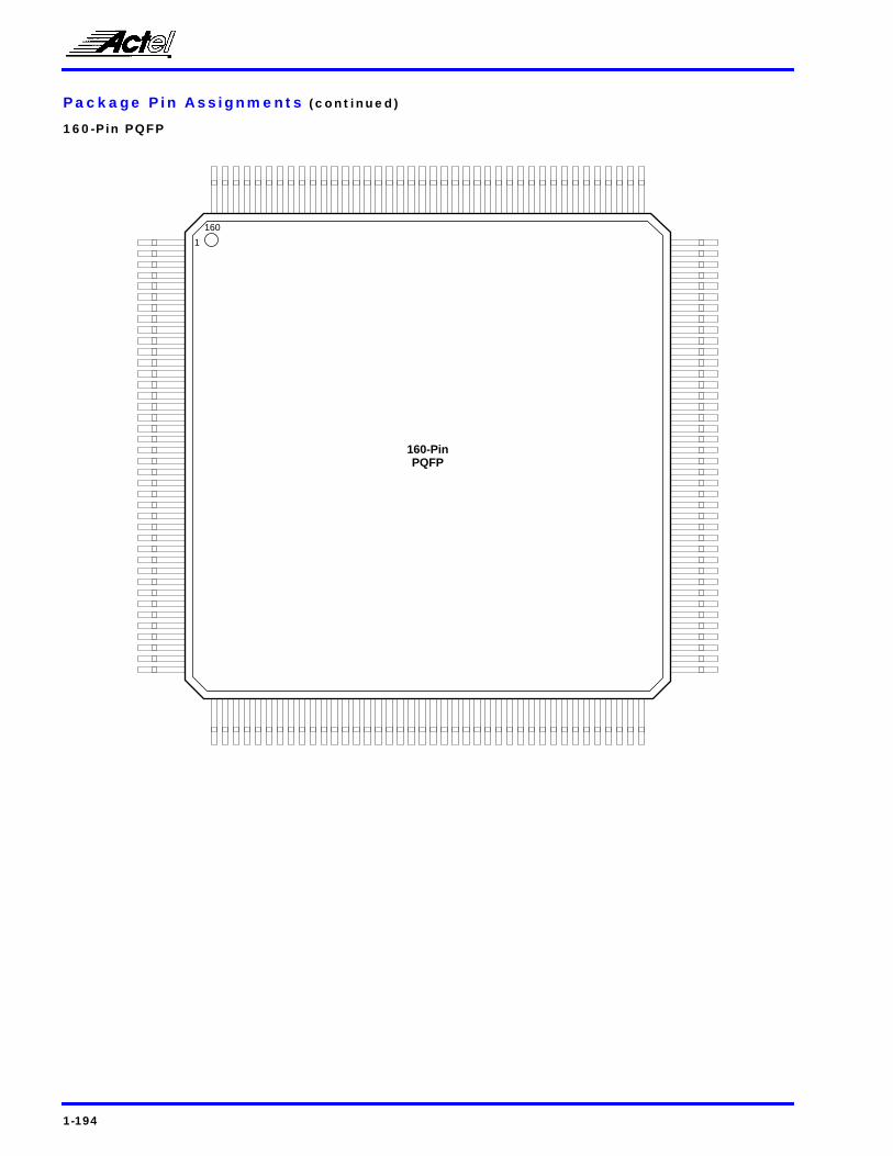
Package Pin Assignments (continued)
160-Pin PQFP
160
1
160-Pin PQFP

1-195
ACT™ 2 Family FPGAs
AC
T2
1
160-Pin PQFP
Pin Number A1280A Function Pin Number A1280A Function
2 DCLK, I/O 69 GND
6 VCC 80 GND
11 GND 86 VCC
16 PRB, I/O 89 GND
18 CLKB, I/O 98 VCC
20 VCC 99 GND
21 CLKA, I/O 109 GND
23 PRA, I/O 114 VCC
30 GND 120 GND
35 VCC 125 GND
38 SDI, I/O 130 GND
40 GND 135 VCC
44 GND 138 VCC
49 GND 139 VCC
54 VCC 140 GND
57 VCC 145 GND
58 VCC 150 VCC
59 GND 155 GND
60 VCC 159 MODE
61 GND 160 GND
64 GND
Notes:1. All unlisted pin numbers are user I/Os.2. MODE pin should be terminated to GND through a 10K resistor to enable Actionprobe usage, otherwise it can be terminated directly to GND.

1-196
Package Pin Assigments (continued)
100-Pin VQFP
1
100-Pin VQFP
100

1-197
ACT™ 2 Family FPGAs
AC
T2
1
100-Pin VQFP
Pin Number A1225A Function Pin Number A1225A Function
2 MODE 65 VCC
7 GND 70 GND
14 VCC 77 SDI, I/O
15 VCC 82 GND
20 GND 85 PRA, I/O
32 GND 87 CLKA, I/O
38 VCC 88 VCC
44 GND 90 CLKB, I/O
55 GND 92 PRB, I/O
62 GND 94 GND
63 VCC 100 DCLK, I/O
64 VCC
Notes:1. All unlisted pin numbers are user I/Os.2. MODE pin should be terminated to GND through a 10K resistor to enable Actionprobe usage, otherwise it can be terminated directly to GND.

1-198
Package Pin Assignments (continued)
176-Pin TQFP
1
176-Pin TQFP
176

1-199
ACT™ 2 Family FPGAs
AC
T2
1
176-Pin TQFP
Pin Number A1240A Function A1280A Function Pin Number A1240A Function A1280A Function
1 GND GND 101 NC NC
2 MODE MODE 103 NC I/O
8 NC NC 106 GND GND
10 NC I/O 107 NC I/O
11 NC I/O 108 NC I/O
13 NC VCC 109 GND GND
18 GND GND 110 VCC VCC
19 NC I/O 111 GND GND
20 NC I/O 112 VCC VCC
22 NC I/O 113 VCC VCC
23 GND GND 114 NC I/O
24 NC VCC 115 NC I/O
25 VCC VCC 116 NC VCC
26 NC I/O 121 NC NC
27 NC I/O 124 NC I/O
28 VCC VCC 125 NC I/O
29 NC I/O 126 NC NC
33 NC NC 133 GND GND
37 NC I/O 135 SDI, I/O SDI, I/O
38 NC NC 136 NC I/O
45 GND GND 140 NC VCC
52 NC VCC 143 NC I/O
54 NC I/O 144 NC I/O
55 NC I/O 145 NC NC
57 NC NC 147 NC I/O
61 NC I/O 151 NC I/O
64 NC I/O 152 PRA, I/O PRA, I/O
66 NC I/O 154 CLKA, I/O CLKA, I/O
67 GND GND 155 VCC VCC
68 VCC VCC 156 GND GND
74 NC I/O 158 CLKB, I/O CLKB, I/O
77 NC NC 160 PRB, I/O PRB, I/O
78 NC I/O 161 NC I/O
80 NC I/O 165 NC NC
82 NC VCC 166 NC I/O
86 NC I/O 168 NC I/O
89 GND GND 170 NC VCC
96 NC I/O 173 NC I/O
97 NC I/O 175 DCLK, I/O DCLK, I/ONotes:1. NC: Denotes No Connection2. All unlisted pin numbers are user I/Os.3. MODE pin should be terminated to GND through a 10K resistor to enable Actionprobe usage, otherwise it can be terminated directly to GND.

1-200
Package Pin Assignments (continued)
172-Pin CQFP
Pin Number A1280A Function Pin Number A1280A Function
1 MODE 107 VCC
7 GND 108 GND
12 VCC 109 VCC
17 GND 110 VCC
22 GND 113 VCC
23 VCC 118 GND
24 VCC 123 GND
27 VCC 131 SDI, I/O
32 GND 136 VCC
37 GND 141 GND
50 VCC 148 PRA, I/O
55 GND 150 CLKA, I/O
65 GND 151 VCC
66 VCC 152 GND
75 GND 154 CLKB, I/O
80 VCC 156 PRB, I/O
98 GND 161 GND
103 GND 166 VCC
106 GND 171 DCLK, I/ONotes:1. All unlisted pin numbers are user I/Os.2. MODE pin should be terminated to GND through a 10K resistor to enable Actionprobe usage, otherwise it can be terminated directly to GND.
172-Pin CQFP
Pin #1 Index
172
1

1-201
ACT™ 2 Family FPGAs
AC
T2
1
Package Pin Assigments (continued)
100-Pin CPGA
Pin Number A1225A Function Pin Number A1225A Function
A4 PRB, I/O E11 VCC
A7 PRA, I/O F3 VCC
B6 VCC F9 VCC
C2 MODE F10 VCC
C3 DCLK, I/O F11 GND
C5 GND G1 VCC
C6 CLKA, I/O G3 GND
C7 GND G9 GND
C8 SDI, I/O J5 GND
D6 CLKB, I/O J7 GND
D10 GND K6 VCC
E3 GND
Note:1. All unlisted pin numbers are user I/Os.2. MODE pin should be terminated to GND through a 10K resistor to enable Actionprobe usage, otherwise it can be terminated directly to GND.
1
A
2 3 4 5 6 7 8 9 10 11
B
C
D
E
F
G
H
J
K
L
A
B
C
D
E
F
G
H
J
K
L
100-Pin CPGA
1 2 3 4 5 6 7 8 9 10 11
Orientation Pin

1-202
Package Pin Assignments (continued)
132-Pin CPGA
Pin Number A1240A Function Pin Number A1240A Function
A1 MODE G2 VCC
B5 GND G3 VCC
B6 CLKB, I/O G4 VCC
B7 CLKA, I/O G10 VCC
B8 PRA, I/O G11 VCC
B9 GND G12 VCC
B12 SDI, I/O G13 VCC
C3 DCLK, I/O H13 GND
C5 GND J2 GND
C6 PRB, I/O J3 GND
C7 VCC J11 GND
C9 GND K7 VCC
D7 VCC K12 GND
E3 GND L5 GND
E11 GND L7 VCC
E12 GND L9 GND
F4 GND M9 GNDNotes:1. All unlisted pin numbers are user I/Os.2. MODE pin should be terminated to GND through a 10K resistor to enable Actionprobe usage, otherwise it can be terminated directly to GND.
132-Pin CPGA
A
B
C
D
E
F
G
H
J
K
L
M
N
A
B
C
D
E
F
G
H
J
K
L
M
N
Orientation Pin
1 2 3 4 5 6 7 8 9 10 11 12 13
1 2 3 4 5 6 7 8 9 10 11 12 13

1-203
ACT™ 2 Family FPGAs
AC
T2
1
Package Pin Assignments (continued)
176-Pin CPGA
Pin Number A1280A Function Pin Number A1280A Function
A3 CLKA, I/O H2 VCC
B3 DCLK, I/O H3 VCC
B8 CLKB, I/O H4 GND
B14 SDI, I/O H12 GND
C3 MODE H13 VCC
C8 GND H14 VCC
C9 PRA, I/O J4 VCC
D4 GND J12 GND
D5 VCC J13 GND
D6 GND J14 VCC
D7 PRB, I/O K4 GND
D8 VCC K12 GND
D10 GND L4 GND
D11 VCC M4 GND
D12 GND M5 VCC
E4 GND M6 GND
E12 GND M8 GND
F4 VCC M10 GND
F12 GND M11 VCC
G4 GND M12 GND
G12 VCC N8 VCCNotes:1. All unlisted pin numbers are user I/Os.2. MODE pin should be terminated to GND through a 10K resistor to enable Actionprobe usage, otherwise it can be terminated directly to GND.
1
A
2 3 4 5 6 7 8 9 10 11
B
C
D
E
F
G
H
J
K
L
176-Pin CPGA
1 2 3 4 5 6 7 8 9 10 11
12
12
13
13
14
14
15
15
M
N
P
R
A
B
C
D
E
F
G
H
J
K
L
M
N
P
R

1-204