a 50nw, 100kbps clock/data recovery circuit in an fsk rf ... · pwr. mgmt. rf rx tx energy...
TRANSCRIPT

26th International Conference on VLSI
January 2013
Pune,India
A 50nW, 100kbps Clock/Data Recovery Circuit in an FSK RF Receiver on a Body
Sensor Node Aatmesh Shrivastava1, Jagdish Pandey2, Brian Otis2, Benton H. Calhoun1 1University of Virginia, Charlottesville 2University of Washington, Seattle

2/25/2013 © VLSI Design Conference 2013 2
Body Sensor Node (BSN)
Ex :- Fan Zhang et al. ”A batteryless 19μW
MICS/ISM-band energy harvesting body area
sensor node SoC.” ISSCC 2012
Features • BSNs promise to change the way
we experience life • Comprehensive and unobtrusive
human health monitoring. Needs • Small Form Factor, light wait • Runs on harvested energy ( Body
heat) • Low cost. • Ultra Low Power

BSN
2/25/2013 © VLSI Design Conference 2013 3
AFE ADC
µController
Memory
DSP
Pwr. Mgmt.
RF
Rx
Tx
Energy Harvester
Boost
Converter
Voltage
Regulation
TEG
Energy Harvesting BSN Soc [1]
ECG,EEG,EMG Fan Zhang et al. ”A
batteryless 19μW
MICS/ISM-band energy
harvesting body area
sensor node SoC.”
ISSCC 2012
• Harvests Energy using TEG from body Heat • AFE, ADC, DSP, etc. performs sensing • RF Rx, Tx used for communication. • Average power consumption 19µW. • In this paper we talk about CDR circuit in the RF receiver

Outline
• BSN RF Receiver – CDR Requirements
• Clock Recovery
• Data Recovery – Phase Detection
– Timing
– Sensitivity
– Control
• Limitations
• Measurement
• Comparison
• References
2/25/2013 © VLSI Design Conference 2013 4

BSN RF Receiver
2/25/2013 © VLSI Design Conference 2013 5
• [2] shows 9 phase injection locked Rx and all digital FSK Demod. • It does not show CDR, needed to recover Data for DSP • In this paper we talk about CDR circuit in the RF receiver
9 Phase Injection
Locked Rx
All Digital
FSK DemodCDR
To Instruction
Memory
Receiver Data Path
Rx OutEye of FSK DemodRecovered Eye
Jitter
Received Signal at various stages
Described in [2]
J. Pandey, et al “A
120μW MICS/ISM-band
FSK receiver with a
44μW …..
multiplication”, ISSCC
2011

CDR Requirements for BSN
2/25/2013 © VLSI Design Conference 2013 6
• Conventional approach in designing CDR usually involves a design of PLLs or DLLs
• These solutions are too expensive in terms of area and power for a BSN. Ex:- [4] uses PLL with 110µW Power >> our SoC Power of 19µW.
• All digital FSK Demod is used in [2] to save power
• A low power, lower cost and lower area CDR circuit is needed for BSN

Clock Recovery
2/25/2013 © VLSI Design Conference 2013 7
• Conventionally CLk is recovered from signal, uses PLL
• In our BSN, Data at 100kB/s, 200khz XTAL for Tx
• Also SoC clock for DSP 200khz from XTAL.
• SoC clock is used to recover data, eliminating a PLL.
Conventional CDR
Phase Detector Loop Filter
VCO
Recovered Data
Received Signal
Recovered clock

Data Recovery Phase Detection
2/25/2013 © VLSI Design Conference 2013 8
• Pulse generated at each point in delay line. • Feeds to D-Flip Flop (DFF) clocked at 200 kHz.
• The pulse close to the edge of the clock will be caught by FF.
Point indicating data in phase with clock
• A number of these phase detectors are placed in series
CLK CLK CLK
1 2 N
Phase Detector
CLK
100
CLK
DATA
PULSE-1
TDPULSE-N
Delayed DATA
In phase
with CLK

Timing requirement
2/25/2013 © VLSI Design Conference 2013 9
• To catch at least one of the pulses, pulse width should meet the following criteria
• TD/2>(THOLD+TSETUP) • This criteria is met for most of
the process points.
Design Margin
Missed
Pulse
CLK
Phase Detector
DATA
TD/2 PULSE_N PULSE_N-1
CLK TSETUP THOLD

XOR Gate in pulse generator
2/25/2013 © VLSI Design Conference 2013 10
• XOR gate is critical to the performance of the PD, we used a transmission gate XOR
• It has much better performance at 500mV than the standard cell XOR.
• The transmission gate XOR has mean delay of 5ns and an area of 3.6x6.0 µm2. The standard cell based XOR has a mean delay of 36ns and area of 3.6x8.0 µm2.
XOR gate used in PD
B
A
Delay of Transmission gate in XOR Delay of XOR gate in Std. Cell
O
Transmission gate XOR

Sensitivity of Phase Detection
2/25/2013 © VLSI Design Conference 2013 11
• One buffer delay sets the sensitivity of the delay line. Lower sensitivity will reduce the amount of input jitter that the CDR circuit can tolerate.
• The mean is close to 1% of the data rate period. • we used 100 stages in the delay line.
Resolution of Delay Line
Of data rate

Sensitivity : Design Tradeoff
2/25/2013 © VLSI Design Conference 2013 12
• Increasing VDD decreases delay through the buffer. This improves the sensitivity but increases the area and power.
• VDD~0.5V has 1% sensitivity, 1000X lower area, and 1000X lower power than at 1.2V. The SoC [1] digital VDD is also 0.5V, so it was used for the CDR circuit.
Power, Area and Sensitivity tradeoff
1000x
1000x

Control Circuit
2/25/2013 © VLSI Design Conference 2013 13
• If OR_N-1=0 and the output of DFF goes high, then the transmission gate Tx turns ON, selecting that output of the delay line.
• It indicates that data is in phase with lock
CLK
N
OUT
OR_NOR_N-1
DATA_N-1 DATA_N
Tx

2/25/2013 © VLSI Design Conference 2013 14
• Once the data has been brought in phase with clock, the CDR goes into lock for the period of of Tx.
• Once a transmission ends, the CDR resets and is now ready for the
next transmission. Timing Diagram CDR
CLK
CLKIN
DATA
DATA_N
OUT
OROUT
In phase
with CLK
Sampled again
at falling edge
OROUT goes high indicating calibration
FF CLK gated to save power
CLK
Complete Circuit Diagram
DATA
1 2 100
RST
CLK
RST
CLK
RSTCLKIN
CTRL1 CTRL2 CTRL100
CTRL1
CTRL2
CTRL100
OROUT
RSTCLKIN
RETENTION
BLOCK
OUT
RST
OR1OR2

Limitations of the Design
2/25/2013 © VLSI Design Conference 2013 15
Clock difference b/w Rx and Tx • clock recovery is not adapted continually, lowers the BER
• Account for the offset between the Tx and Rx clock frequencies.
• Rx and Tx are generated from Xtal, maximum offset of 50ppm [6]
, setting inherent BER of CDR to 5x10⁻⁵.
• This does not significantly degrade the overall BER of the link, which is set by the RX and is 10-3 [2].
• This also illustrates that explicit clock recovery is not needed in this case

Limitations of the Design
2/25/2013 © VLSI Design Conference 2013 16
Process variation of total Delay of the delay line • A second limitation is that the total delay of the delay line
should be greater than 5µs for this circuit to work correctly.
• Since the delay in sub-threshold varies exponentially with process variation, the spread of the total delay will be very large.
• We can compensate variation by lengthening the delay line or by reducing VDD slightly.

Limitations of the Design
2/25/2013 © VLSI Design Conference 2013 17
Metastability • It is also possible that the DFF in one of the phase
detectors can enter a meta-stable state during calibration, increasing power consumption briefly.
• However, this probability is very low due to noise (thermal, flicker etc.) and the 2.5µs hold period.

Measurement
2/25/2013 © VLSI Design Conference 2013 18
• In the measurement test we measured eye diagram of the FSK demod out and the CDR data out for a 27-1 pseudo random data sequence running through the RX at a data rate of 100 kbps.
• The FSK demod output has a jitter of ~2µs, while the data recovery circuit recovers the data with a jitter of 16ns.

Design Comparison
2/25/2013 © VLSI Design Conference 2013 19
Design Comparison
[3] [4] [5] This Work
Technology 90nm 0.25µm 0.18µm 0.13µm
Data Rate 200kb/s 2Mb/s 10Mb/s 100kb/s
Acquisition Time 54µs 45µs - 2.5µs
Power (CDR) 217nW 112µW 8.05µW 50nW
Energy/bit 1pJ 56pJ 0.8pJ 0.5pJ
Area ( mm2) 0.035 - 0.09 0.017
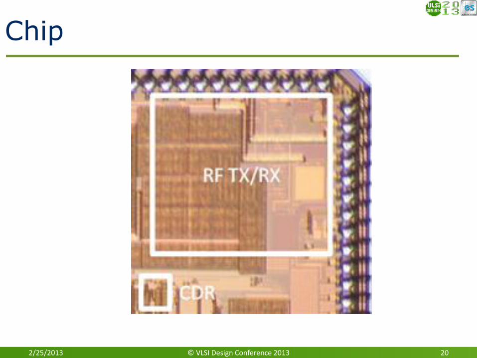
Chip
2/25/2013 © VLSI Design Conference 2013 20

Conclusion
2/25/2013 © VLSI Design Conference 2013 21
• We presented a low power CDR circuit for a wireless body sensor node.
• It consumes 50nW at 100kbps or 0.4pJ/bit.
• Recovers data from FSK demod of the receiver with upto 2µs jitter. It locks over 18X faster than prior art.
• The proposed circuit is fabricated in a 0.13µm CMOS technology. It can recover data with an input jitter of up to 2.4µs with >2X less power and >2X less area than prior work.
• The proposed circuit is completely implemented using digital gates and can easily be synthesizable.

Acknowledgement
2/25/2013 © VLSI Design Conference 2013 22
This work was supported in part by the NSF NERC ASSIST center (EEC-1160483)

References
2/25/2013 © VLSI Design Conference 2013 23
1. F. Zhang, et. al, “A Battery-less 19µW MICS/ISM-Band Energy Harvesting
Body Area Sensor Node SoC ”, IEEE International Solid State Circuits
Conference, 2012
2. J. Pandey, S. Jianlei and B. Otis, “A 120μW MICS/ISM-band FSK receiver
with a 44μW low-power mode based on injection-locking and 9x frequency
multiplication”, IEEE International Solid State Circuits Conference, 2011
3. T. Kleeburg, J. Loo, N. J. Guilar, E. Fong and R. Amritharajah , “Ultra-low-
voltage circuits for sensor applications powered by free-space optics”, IEEE
International Solid State Circuits Conference, 2010
4. S-J Song, N. Cho, and H-J Yoo, “A 0.2-mW 2-Mb/s Digital Transceiver
Based on Wideband Signaling for Human Body Communications”, IEEE
Journal on Solid State Circuit, September 2007
5. S. Kim, et. al, “A low-power referenceless clock and data recovery circuit
with clock-edge modulation for biomedical sensor applications”, IEEE
International Symposium on Low Power Electronics and Design, 2007
6. LQXO-4 Oscillator, Low Power Crystal Oscillator- Datasheet.
SATEKCorporation, ORANGA, CA