a 23-ghz bandwidth automatic gain control amplifier
TRANSCRIPT

Progress In Electromagnetics Research, Vol. 142, 261–273, 2013
A 23-GHz BANDWIDTH AUTOMATIC GAIN CONTROLAMPLIFIER WITH WIDE DYNAMIC RANGE FOR HIGHSPEED COMMUNICATION
Bo Zhang1, *, Yong-Zhong Xiong2, Lei Wang3, Sanming Hu4,and Le-Wei Li5, 6
1Xi’an University of Posts and Telecommunications, Xi’an 710121,China2MicroArray Technologies, Chengdu 611731, China3University of Electronic Science and Technology of China, 611731,China4Institute of Microelectronics, Singapore5Department of Electrical & Computer Systems Engineering, MonashUniversity, Clayton, Victoria 3800, Australia6School of Engineering, Monash University, Sunway, Selangor 46150,Malaysia
Abstract—In this paper, a wide bandwidth and wide dynamic rangeAGC amplifier is presented. A push-pull variable gain amplifier (VGA)structure is proposed for wide dynamic rang. Moreover, the bandwidthenhancement technique is used in the post amplifier design to ensurethe wide bandwidth and gain of whole circuit. The experimentalresults demonstrate that the proposed AGC amplifier fabricated in0.13µm SiGe BiCMOS process, achieves a 23-GHz bandwidth and36-dB dynamic rang whereas the power and area consumption are57.6mW and 1.9 mm2, respectively.
1. INTRODUCTION
The rapid growth in data communication and multimedia applicationshas been driving research on millimeter-wave frequency band highspeed communication, such as 60-GHz radio system and over 100-GHzmillimeter wave communication system [1–7]. In order to provide high
Received 20 June 2013, Accepted 10 August 2013, Scheduled 4 September 2013* Corresponding author: Bo Zhang ([email protected]).

262 Zhang et al.
enough data rate with smaller equipment size and lower price, thedemand for high speed integrated circuits (ICs) operating at tens ofGbps remains unremitting. Traditionally, these high speed circuits aremainly designed in III-V compound semiconductor technologies [5–7].The III-V compound semiconductor is assumed a good candidate forhigh frequency operation. However, due to its incompatibility withcommonly used low-cost CMOS intermediate frequency or base-bandcircuit and high fabrication cost, the III-V compound semiconductor isnot the best choice for integrated system-on-chip (SoC) circuit design.Among the technologies for high-speed circuits, the SiGe HBT, in fact,becomes a favorable candidate due to its compatibility with CMOSbase-band circuits and of course, its good high frequency performance.
At the receiving end, the signal can vary over a wide range. Inorder to sustain the operation of the subsequent baseband circuits,weak signal has to be amplified and an overly-large signal must bedepressed. To fulfill the requirement, an AGC amplifier is necessary inhigh speed communication systems , due to its advantage of noise andjitter compared to a limiting amplifier (LA) [8–13]. Wide bandwidthand dynamic range are the most important considerations in AGCamplifier design of high speed receiver. Recently, a 10 Gbps AGCamplifier that offers a 35-dB dynamic range is demonstrated in 0.18µmCMOS technology [14]. However, the bandwidth of the circuit is stillinsufficient for modern high speed communication. A 40 Gbps AGCamplifier has also been fabricated in 90-nm CMOS technology [15] butits performance is still inadequate in some applications. To achieve anAGC with wide dynamic range, the requirement of wide bandwidthand high gain is thus a tall order for modern wireless and optical highspeed communications.
This paper presents a new VGA structure to achieve a widedynamic range with higher gain. Using the proposed VGA core, theAGC amplifier is able to realize wider dynamic range with highergain and lower power consumption. In addition, the bandwidthenhancement and multi-stage peak detection techniques are bothemployed to extend the bandwidth. The circuit, occupying an areaof 1.9 mm2, is fabricated in 0.13µm SiGe BiCMOS technology.
2. AGC AMPLIFIER ARCHITECTURE
2.1. Push-pull Variable Gain Amplifier
The architecture of the AGC amplifier is shown in Fig. 1. In AGCamplifier design, the VGA plays a very important role. Almost allpopularly used VGAs for high speed data transmission developed fromthe differential pair and control their gain through varying the tail

Progress In Electromagnetics Research, Vol. 142, 2013 263
VGA
Peak Detector
Gain Control
Post
Amplifier Buffer
A2Input Output
Figure 1. Architecture of the AGC amplifier.
current source. This approach raises some concerns, such as the narrowgain control range and limitation of dynamic range of whole AGCcircuit. In order to solve these issues, a new control scheme variablegain amplifier is proposed in this work and the architecture of theproposed VGA is provided in Fig. 2.
Figure 2. Architecture of proposed push-pull VGA.
From Fig. 2, it can be seen that the input signal is applied tothe transistor pair T1 and T2, and the gain control signal is connectedto transistors T3, T4 and T5. The Compared with the conventionalGilbert Cell-based VGA, an additional transistor T5 is used to controlthe gain of the circuit. In previous designs, the common emitter pairis often used to control the gain. However, the dynamic range of theamplifier will be impacted when the bias of common emitter pair isaltered. In this work, when the input signal is applied to the inputports, the bias of the common emitter pair (T1 and T2) is maintained

264 Zhang et al.
to ensure a constant current source, and the gain is controlled by theadditional transistor, T5 and the common base pair, T3 and T4. WhenVctrl1 is set to low level, the transistor T3 and T4 will operate at cut-off region. If Vctrl1 is set to high level, the transistor of T3 and T4
will operate at forward-active region. On the other hand, when Vctrl2
is set to low level, the transistor T5 also operates at cut-off region,while it will operates at forward-active region when Vctrl2 is set tohigh level. In proposed circuit, the dynamic range of VGA is mostlydependent on the common emitter pair which is kept a constant biassource, so the dynamic range cannot be degraded when the gain of thewhole VGA is varying. In addition, the adjustment time of the wholecircuit is saved due to the push-pull structure. As a trade-off amongpower gain, dynamic range and linearity, T1 and T2 are chosen as 084 4transistor, meanwhile T3, T4 and T5 are chosen as 048 4 transistor. Inaddition, the load resistor RL is set to 150 ohm.
In order to elucidate the working principle of our proposed VGA,the simplified half-circuit of proposed VGA core is illustrated in Fig. 3.It can be seen that the input signal is applied to transistor T1, and theoutput current is divided through transistors T2 and T3. Hence, theoutput current which goes through transistor T2 can be calculated asfollow:
Io2 = gm1VIN1
1 + gm3/gm2(1)
where gm1, gm2 and gm3 are the transconductances of transistors T1,
Figure 3. Simplified half-circuit of proposed VGAcore.
Figure 4. Voltage gain of simplifiedhalf-circuit of proposed VGA versus gm3.

Progress In Electromagnetics Research, Vol. 142, 2013 265
T2 and T3. The voltage gain of the VGA can be expressed as:
AV =∣∣∣∣Vout
Vin
∣∣∣∣ =gm1RL
1 + gm3/gm2(2)
where RL is the output load resistor. From the above equations, it isclear that the increase of transconductance, gm1 and gm2 will lead to anenhancement of the gain of the whole circuit. On the other hand, if gm3
is raised, the gain of whole circuit will drop. The transconductancesof the transistors are controlled by both Vctrl1 and Vctrl2. If Vctrl1 ismade larger, transconductance gm2 will increase and Vctrl2 will decreaseaccordingly to lower transconductance gm3. So the gain of whole VGAincreases quickly while gm1 is maintained at a constant value. Thevoltage gain of simplified half-circuit of proposed VGA versus gm3 isshown in Fig. 4. In VGA design, the dynamic range of the wholeamplifier depends mostly on transistor T1. In proposed design, gm1 iskept at a constant and both gm2 and gm3 are used to control the gainof whole amplifier. So by using this new push-pull VGA structure, thecircuit gain can quickly be varied with wider gain control range andno degradation of the dynamic range.
2.2. Broadband Post Amplifier
In order to obtain sufficient gain, the VGA core is assisted by athree-stage post amplifier. Since the bandwidth of the entire circuitis expected to be very wide to provide enough high data rate, thebandwidth of post amplifier must fulfill the requirement of gain andbandwidth. In conventional amplifier design, the bandwidth is mainlydetermined by the RC time constants of every node. To enhance thebandwidth of the post amplifiers, the series inductor technique is addedbetween stages.
The schematic diagram of our proposed post amplifier and alsothe small-signal equivalent circuit of the amplifier with series inductorare shown in Fig. 5 and Fig. 6. The L is deployed inductor, C1 andC2 are the equivalent capacitance by previous stage and next stage,R1 and R2 are the equivalent resistance by previous stage and nextstage. The transfer function of the proposed amplifier is calculated inEquation (3). It is noted that the inductor and parasitic capacitancesconstruct a third-order LC-ladder which could extend the bandwidth ofwhole amplifier. The 3-dB bandwidth of the proposed amplifier couldbe obviously extended as compare to conventional amplifier structureby adding the series inductor between stages [16], especially for themultistage cascaded structure. As a trade-off of bandwidth, powergain and stability, T1 and T2 are chosen as 084 4 transistor, meanwhile

266 Zhang et al.
Figure 5. One stage of postamplifier.
L
R1 C1 C2 R2OutputInput
Stage1 Stage2
Figure 6. Equivalent inter-stage small signal modal of postamplifier.
the inductor is set to 0.25 nH and 0.45 nH for different stages.Vout
Vin=
−gm1R1R2
R1 + R2 + s [R1R2(C1 + C2) + L]
+s2R1R2L[
C2R1
+ C1R2
]+ s3R1R2C1C2L
(3)
2.3. Peak Detector and Control Voltage Generation
In AGC amplifier design, another important circuit is the peakdetector, which will be used for generating the control voltage andthen control the gain of whole circuit [17]. The detector of our proposedAGC amplifier is realized through a two-stage peaking detector circuitand the schematic is as shown in Fig. 7. T1, T2, T8 and T9 are chosenas 084 4 transistor, meanwhile T15 is chosen as 048 4 transistor. Inaddition, R is set to 200 ohm and C1, C2 are set to 15 pF, respectively.
The input signal Vin is applied to transistor T1, and when Vin
exceeds the peak voltage Vpeak, transistor T1 is switched on. Thecurrent that follows is copied by the current mirror, T5 and T6, tocharge the holding capacitor C1. On the other hand, when the inputsignal Vin is below Vpeak, transistor T1 is switched off and the capacitorC1 holds the peak voltage. In our VGA design, the push-pull controlvoltage is used for extending the controlling range and increasing theadjusting speed. Hence, two control voltages must be generated bythe detector design. Based on the above requirements, transistor T15
is added alongside the output holding capacitor. At the output oftransistor T15, the phase-opposite control voltages Vpd1 and Vpd2 to the

Progress In Electromagnetics Research, Vol. 142, 2013 267
Figure 7. Architecture of peaking detector and control voltages Vpd1
and Vpd2 generation circuit.
peak voltage Vpeak is generated. The push-pull control voltage can bederived as follows:
Vctrl1 = k
(Vref
Vpd1
)(4)
Vctrl2 = k
(Vref
Vpd2
)(5)
Vpd2 = Vref − Vpd1 (6)
where k is a constant coefficient and Vref a reference voltage, which isrelated to the output power and independent of the input voltage.In addition, to obtain a constant settling time, a log amplifier isused for generating the control voltage [11]. Because of the BiCMOSprocess employed, the log amplifier can easily be constructed usingBJT transistors.
Finally, in order to drive the output with a 50-Ω load, a two-stage output buffer is employed. The output buffer is realized usingthe differential configuration with active load, and the bandwidthenhancement technique is also employed to extend the bandwidth.
3. RESULTS AND DISCUSSION
The whole AGC amplifier is designed and fabricated in 0.13µm SiGeHBT BiCMOS technology with an fT of 200-GHz and fMAX of 250-GHz. The fabricated chip microphotography is given in Fig. 8. Thesize of the whole switch modulator, which includes the test pads, is830µm× 2300µm.

268 Zhang et al.
VGA Core
Control Voltage
Generation
Post Amplifier Output Buffer
Figure 8. Microphotography of AGC amplifier.
Figure 9. Measurement setup.
The experimental setup shown in Fig. 9 is used to measurethe S-parameter and time-domain response of whole AGC amplifier.The equipment for on-chip measurement consists of signal generator,tunable attenuator, oscilloscope and vector network analyzer. Theinput signal of time domain measurement comes from the patterngenerator and a continuous tunable attenuator connected by coaxialcable and ground-signal-ground (GSG) probe. The power level of inputsignal can be controlled by the attenuator and calibrated through apower meter. As a drawback, the attenuator will introduces somedistortions and noises, which impact the input signal of device-under-test (DUT). The measurement equipments are calibrated by usingline-reflect-reflect-match (LRRM) calibration with a ceramic standardsubstrate to compensate the impacts of connection components andprobes and then make the reference plane to the probe tip.
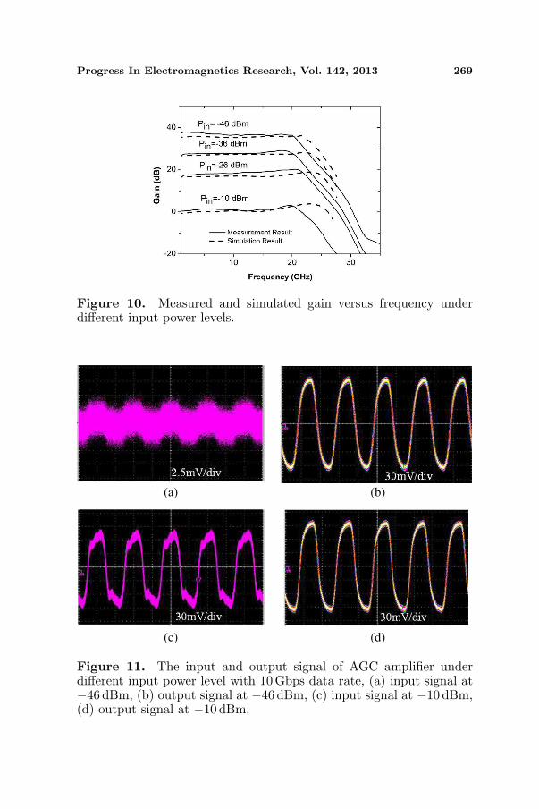
The simulated and measured gain versus frequency characteristicsunder different input power level is presented in Fig. 10. Fromthe figure, it can be seen that the 3-dB bandwidth of the proposedAGC amplifier is about 23-GHz, which can be used for over 30 Gb/s
Progress In Electromagnetics Research, Vol. 142, 2013 269
Figure 10. Measured and simulated gain versus frequency underdifferent input power levels.
(a) (b)
(c) (d)
Figure 11. The input and output signal of AGC amplifier underdifferent input power level with 10 Gbps data rate, (a) input signal at−46 dBm, (b) output signal at −46 dBm, (c) input signal at −10 dBm,(d) output signal at −10 dBm.

270 Zhang et al.
signal transmission. The differences between measurement results andsimulation results at high frequency due to the capacitive parasiticeffect of the layout and test pad. The gain of whole AGC amplifieris automatically adjusted to achieve a constant output voltage of200mVpp while the input power level is swept from −46 dBm to−10 dBm. The maximum gain of the AGC amplifier is 36-dB. Inaddition, all the gain curves derived for different input signals are alsonoted to be very smooth. The fluctuation in the bandwidth is smallerthan 1 dB and this is very important for high speed signal transmission.The measured dynamic range of the whole AGC amplifier is about36 dB. The entire circuit draws 32 mA current from the 1.8 V supplyvoltage.
The time domain response is measured up to 10 Gbps, whichis limited by the measurement equipment. The input and outputsignal diagram of AGC amplifier at different input power level with10Gbps data rate is shown in Fig. 11. The input swing is sweptfrom 3.2mVpp to 200 mVpp. Accordingly, the power level is sweptfrom −46 dBm to −10 dBm at 50 Ω. The different power level inputsignal is generated by the pattern generator and attenuator. It isnoted that due to the unexpected impacts of attenuator, the inputsignal is not very good. However, after the processing of proposedAGC amplifier, the output signals achieve same size and very clearcurve. Fig. 12 shows the measured output eye pattern for 10Gbpsinput. The signal generator is used to generate the input pulse of 231-1 pseudorandom bitstream. The measurement is performed in singleend mode and the other input/output ends are terminated by a 50-Ωresistor. From the figure, a well-opened eye pattern is obtained. Thepeak-to-peak jitter is lower than 7 ps. The VGA is observed to yield
(a) (b)
Figure 12. Single-ended eye-diagram of AGC output under differentinput power level with 10 Gbps data rate, (a) −46 dBm, (b) −10 dBm.

Progress In Electromagnetics Research, Vol. 142, 2013 271
Table 1. High-speed AGC amplifiers performance comparison.
Process
Dynamic
Range
(dB)
Bandwidth
(GHz)
Gain
(dB)
PDC
(mW)
Peak-to-Peak
Jitter (ps)
Area
(mm2)Ref.
Inp-InGaAs
DHBT43 50 17 627 - - [12]
0.13 µm
SiGe40 7.5 30 72 40 1 [13]
0.18 µm
CMOS35 10 21* 54 25 1.3 [14]
90 nm
CMOS19 22 28* 75 - 0.56 [15]
0.13 µm
SiGe36 23 36 57.6 7 1.9
This
work
* Estimates from figures in the corresponding papers.
superior output waveforms when the input signal amplitude varies from3.2mVpp to 200 mVpp. From the simulation result, the settling time ofproposed AGC amplifier is smaller than 0.2µs, while most of previousreported works are larger than 1µs. Finally, the main performance ofthe proposed AGC amplifier is summarized in Table 1 and comparedwith recently published high-speed AGC amplifiers.
4. CONCLUSIONS
An AGC amplifier for high speed communication system is designed.In order to achieve wider dynamic range, a new variable gain amplifieris proposed, and two opposite varying control voltages are deployedto obtain wider control range and the higher adjustment speed, whichis desired in high speed communication. A post amplifier is neededto assure that the whole ACG circuit can acquire sufficient gain. Thebandwidth enhancement technique is employed in the post amplifierdesign for wider bandwidth in the complete AGC amplifier. In orderto generate the push-pull control voltage, the two peak voltages aregenerated using a peak detector circuit. Compared with recentlypublished AGC amplifiers, a superior result has been demonstrated bythe proposed AGC amplifier. This paves the way for tens of gigabitsper second data rate communication.

272 Zhang et al.
ACKNOWLEDGMENT
This work is support by the National Natural Science Foundationof China (Grant No. 61201044), Natural Science Foundation ofShaanxi Province of China (Grant No. 2012JQ8020), Foundationof Shaanxi Educational Committee (Grant No. 12JK0539), Agencyfor Science, Technology and Research (A*STAR), Singapore, underGrant 082 141 0040.
REFERENCES
1. Deng, L., D. Liu, X. Pang, X. Zhang, V. Arlunno, Y. Zhao,A. Caballero, A. K. Dogadaev, X. Yu, I. T. Monroy, M. Beltran,and R. Llorente, “42.13 Gbit/s 16QAM-OFDM photonics-wirelesstransmission in 75–110 GHz band,” Progress In ElectromagneticsResearch, Vol. 126, 449–461, 2012.
2. Yang, M.-H., F.-H. Guan, J. Xu, X. Shi, and X.-W. Sun, “Signalmodel analysis of a 35GHz alternating current direct detectionreceiver,” Progress In Electromagnetics Research, Vol. 88, 275–287, 2008.
3. Dyadyuk, V., J. D. Bunton, J. Pathikulangara, R. Kendall,O. Sevimli, L. Stokes, and D. A. Abbott, “A multigigabitmillimeter-wave communication system with improved spectralefficiency,” IEEE Trans. Microwave Theory Tech., Vol. 55, No. 12,2813–2821, Dec. 2007.
4. Khaddaj Mallat, N., E. Moldovan, and S. O. Tatu, “Comparativedemodulation results for six-port and conventional 60 GHz directconversion receivers,” Progress In Electromagnetics Research,Vol. 84, 437–449, 2008.
5. Hirata, A., T. Kosugi, H. Takahashi, J. Takeuchi, H. Togo,M. Yaita, N. Kukutsu, K. Aihara, K. Murata, Y. Sato,T. Nagatsuma, and Y. Kado, “120-GHz-band wireless linktechnologies for outdoor 10-Gbit/s data transmission,” IEEETrans. Microwave Theory Tech., Vol. 60, No. 3, 881–895,Mar. 2012.
6. Nakasha, Y., M. Sato, T. Tajima, Y. Kawano, T. Suzuki,T. Takahashi, K. Makiyama, T. Ohki, and N. Hara, “W-bandtransmitter and receiver for 10-Gb/s impulse radio with an optical-fiber interface,” IEEE Trans. Microwave Theory Tech., Vol. 57,No. 12, 3171–3180, Dec. 2009.
7. Hirata, A., R. Yamaguchi, T. Kosugi, H. Takahashi, K. Murata,T. Nagatsuma, N. Kukutsu, Y. Kado, N. Iai, S. Okabe, S. Kimura,H. Ikegawa, H. Nishikawa, T. Nakayama, and T. Inada, “10-Gbit/s

Progress In Electromagnetics Research, Vol. 142, 2013 273
wireless link using InP HEMT MMICs for generating 120-GHzband millimeter-wave signal,” IEEE Trans. Microwave TheoryTech., Vol. 57, No. 5, 1102–1109, 2009.
8. Kucharski, D. and K. T. Kornegay, “Jitter considerations inthe design of a 10-Gb/s automatic gain control amplifier,”IEEE Trans. Microwave Theory Tech., Vol. 53, No. 2, 590–597,Feb. 2005.
9. Zhang, B., Y.-Z. Xiong, L. Wang, S. Hu, T.-G. Lim, Y.-Q. Zhuang, and J. L.-W. Li, “A D-band power amplifier with 30-GHz bandwidth and 4.5-dBm psat for high-speed communicationsystem,” Progress In Electromagnetics Research, Vol. 107, 161–178, 2010.
10. Wong, S.-K., F. Kung Wai Lee, S. Maisurah, and M. N. B. Osman,“A wimedia compliant CMOS RF power amplifier for ultra-wideband (UWB) transmitter,” Progress In ElectromagneticsResearch, Vol. 112, 329–347, 2011.
11. Liu, C., Y.-P. Yan, W.-L. Goh, Y.-Z. Xiong, L.-J. Zhang, andM. Madihian, “A 5-Gb/s automatic gain control amplifier withtemperature compensation,” IEEE J. Solid-State Circuits, Vol. 47,No. 6, 1323–1333, Jun. 2012.
12. Lai, J. W., Y.-J. Chuang, K. Cimino, and M. Feng, “Designof variable gain amplifier with gain-bandwidth product up to354GHz implemented in InP-InGaAs DHBT technology,” IEEETrans. Microwave Theory Tech., Vol. 54, No. 2, 599–604,Feb. 2006.
13. Liu, C., Y.-P. Yan, W.-L. Goh, Y.-Z. Xiong, L.-J. Zhang, andM. Madihian, “A 5-Gb/s automatic gain control amplifier withtemperature compensation,” IEEE J. Solid-State Circuits, Vol. 47,No. 6, 1323–1333, Jun. 2012.
14. Liao, C.-F. and S.-I. Liu, “A 10 Gb/s CMOS AGC amplifier with35 dB dynamic range for 10 Gb ethernet,” IEEE ISSCC Dig. Tech.Papers, 516–517, 2006.
15. Liao, C.-F. and S.-I. Liu, “40 Gb/s transimpedance-AGC amplifierand CDR circuit for broadband data receivers in 90 nm CMOS,”IEEE J. Solid-State Circuits, Vol. 43, No. 3, 642–655, Mar. 2008.
16. Wu, C.-H., C.-H. Lee, W.-S. Chen, and S.-I. Liu, “CMOSwideband amplifier using multiple inductive-series peakingtechnique,” IEEE J. Solid-State Circuits, Vol. 40, No. 2, 548–552,Feb. 2005.
17. Park, S.-B., J. E. Wilson, and M. Ismail, “The chip-peak detectorsfor multistandard wireless receivers,” IEEE Circuits and DevicesMagazine, Vol. 22, No. 6, 6–9, Nov. 2006.