1.9 ghz low noise amplifier
TRANSCRIPT
Xavier Edokpa
Dr. Charles Baylis
Baylor University
RF/Microwave Circuits II – Low Noise Amplifier Design
Final Report
April 30, 2015
EDOKPA 2
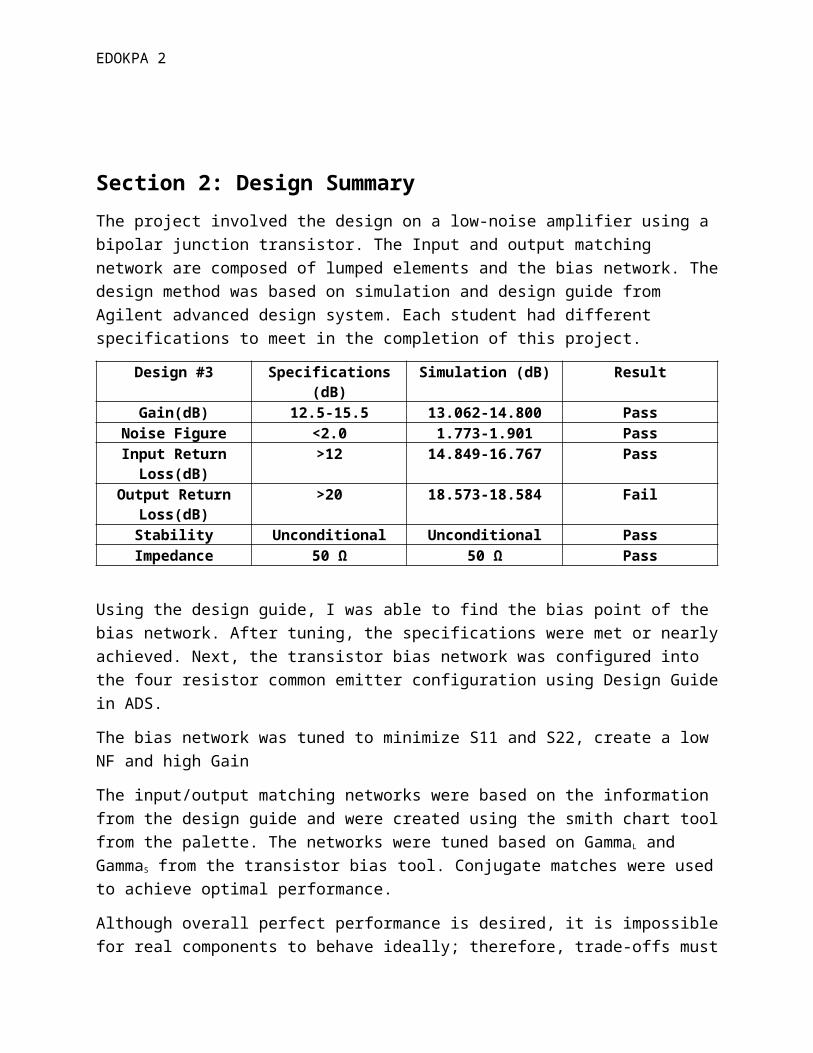
Section 2: Design Summary
The project involved the design on a low-noise amplifier using a bipolar junction transistor. The Input and output matching network are composed of lumped elements and the bias network. The design method was based on simulation and design guide from Agilent advanced design system. Each student had different specifications to meet in the completion of this project.
Design #3 Specifications (dB) Simulation (dB) ResultGain(dB) 12.5-15.5 13.062-14.800 Pass
Noise Figure <2.0 1.773-1.901 PassInput Return Loss(dB) >12 14.849-16.767 Pass
Output Return Loss(dB)
>20 18.573-18.584 Fail
Stability Unconditional Unconditional PassImpedance 50 Ω 50 Ω Pass
Using the design guide, I was able to find the bias point of the bias network. After tuning, the specifications were met or nearly achieved. Next, the transistor bias network was configured into the four resistor common emitter configuration using Design Guide in ADS.
The bias network was tuned to minimize S11 and S22, create a low NF and high Gain
The input/output matching networks were based on the information from the design guide and were created using the smith chart tool from the palette. The networks were tuned based on GammaL and GammaS from the transistor bias tool. Conjugate matches were used to achieve optimal performance.
Although overall perfect performance is desired, it is impossible for real components to behave ideally; therefore, trade-offs must be made. I focused my design around achieving an adequate noise figure, as this specification can be quite difficult to meet when using relatively large shunt resistances to increase stability and output return loss.
Section 3: Stability Analysis
The transistor bias network was designed as a three resistor common emitter configuration as opposed to four resistor network. Upon reflection, the four resistor network likely would have afforded a greater deal of variability in which a proper output return loss could have been achieved through tuning.
Proceeding with the three resistor network, the output matching network was tuned to improve upon S22 whilst maintaining as low a noise figure as possible without compromising the performance of the transistor, or gain. However, this proved to be difficult and led to the tuning of the transistor bias network. The collector resistance, base capacitor, base resistor, output capacitor, and the shunt output resistor were all tuned to optimize noise figure and output return loss and maintain unconditional stability. The matching networks were designed to be a
EDOKPA 3
conjugate match to the inputs/outputs of the active network. This is done to insure stability and gain.
Section 4: Gain, Noise Figure and Input/output Match Analysis
The preliminary design is composed of three different networks: the input matching network, the output matching network, and the active transistor network. In order to achieve minimum noise figure, maximum power transfer and maximum gain of the DUT, the matching networks must be conjugately matched to deliver on the stated requirements. To be conjugately matched, the reflection coefficients of the networks should be the conjugate of the reflection coefficient of the active network at the source and the load, meaning that the imaginary or reactive component of the impedance must be of the opposite value of the impedance seen at the source and load.
Section 5: Design Using Ideal Components
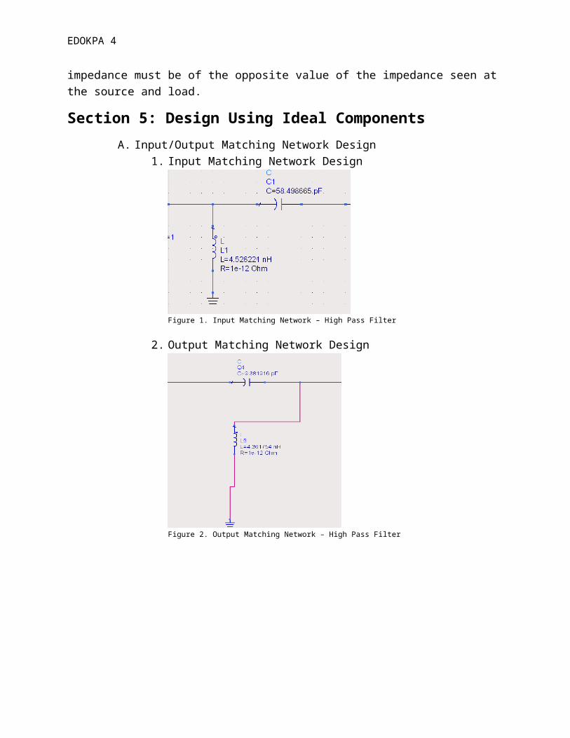
A. Input/Output Matching Network Design1. Input Matching Network Design
Figure 1. Input Matching Network – High Pass Filter
2. Output Matching Network Design
Figure 2. Output Matching Network – High Pass Filter
EDOKPA 4
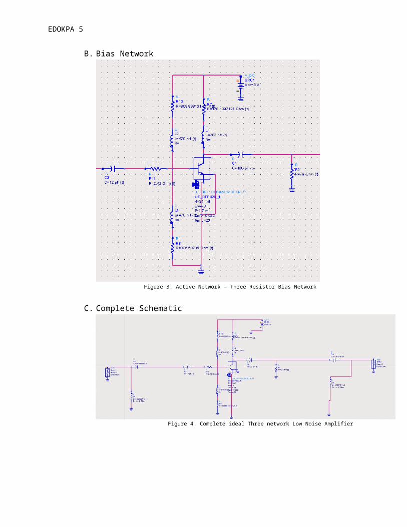
B. Bias Network
Figure 3. Active Network – Three Resistor Bias Network
C. Complete Schematic
Figure 4. Complete ideal Three network Low Noise Amplifier
EDOKPA 5
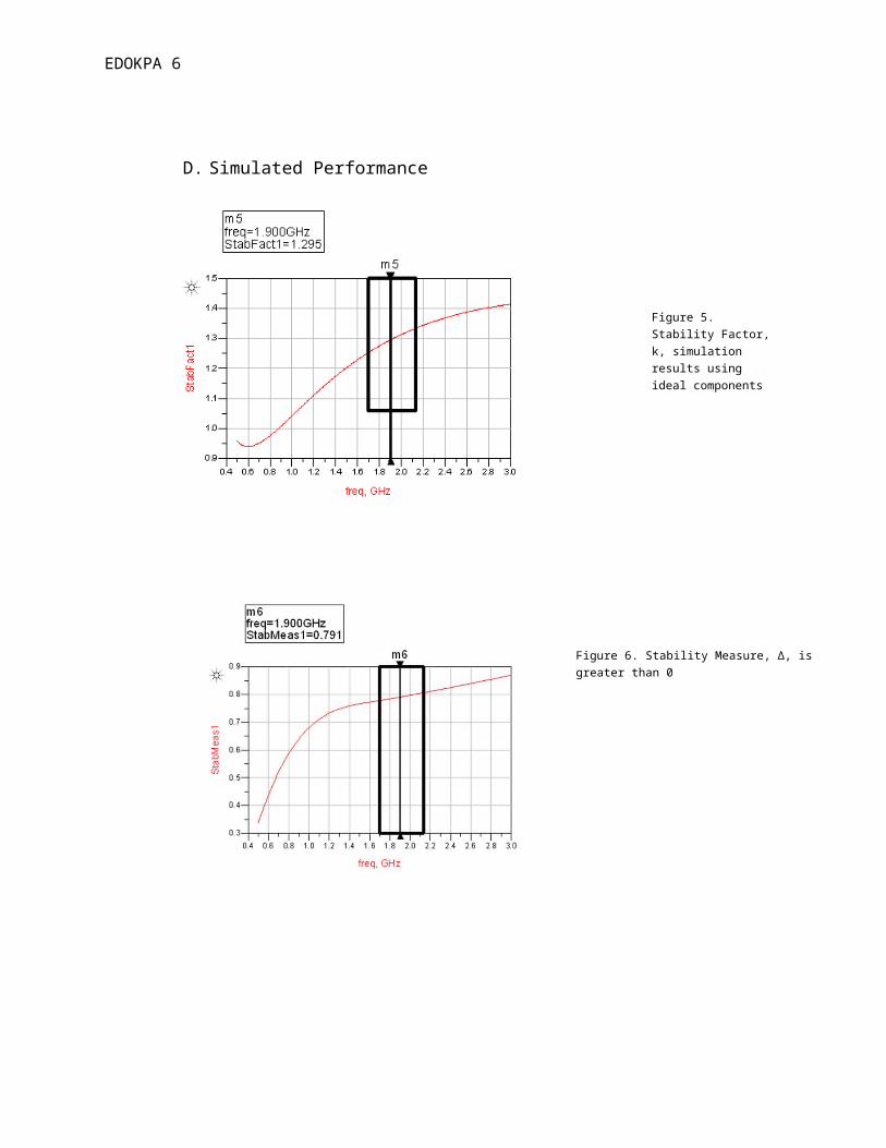
D. Simulated Performance
Figure 5.Stability Factor, k, simulation results using ideal components
Figure 6. Stability Measure, ∆, is greater than 0
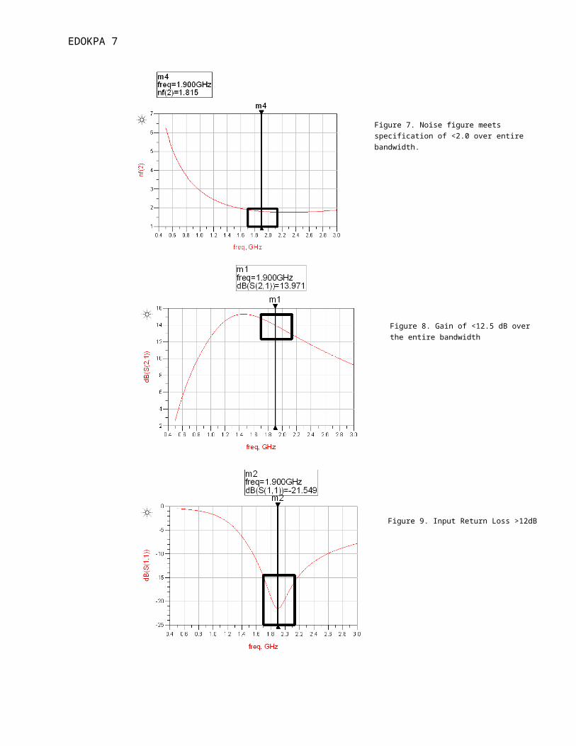
Figure 7. Noise figure meets specification of <2.0 over entire bandwidth.
EDOKPA 6
Figure 8. Gain of <12.5 dB over the entire bandwidth
Figure 9. Input Return Loss >12dB
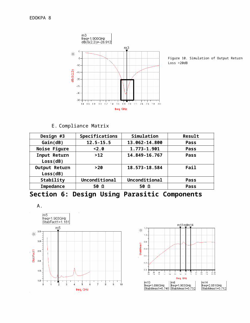
Figure 10. Simulation of Output Return Loss >20dB
EDOKPA 7
E. Compliance Matrix
Design #3 Specifications Simulation ResultGain(dB) 12.5-15.5 13.062-14.800 Pass
Noise Figure <2.0 1.773-1.901 PassInput Return Loss(dB) >12 14.849-16.767 Pass
Output Return Loss(dB)
>20 18.573-18.584 Fail
Stability Unconditional Unconditional PassImpedance 50 Ω 50 Ω Pass
Section 6: Design Using Parasitic Components
A.
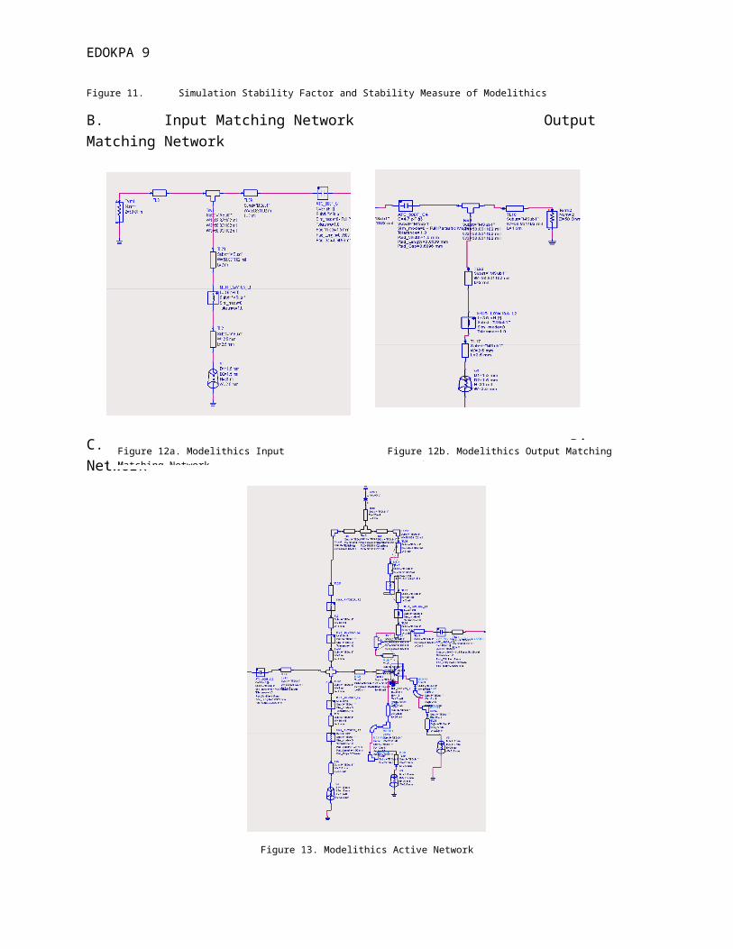
Figure 11. Simulation Stability Factor and Stability Measure of Modelithics
B. Input Matching Network Output Matching Network
Figure 12a. Modelithics Input Matching Network Figure 12b. Modelithics Output Matching Network
EDOKPA 8
C. Bias Network
Figure 13. Modelithics Active Network
D. Complete Schematic
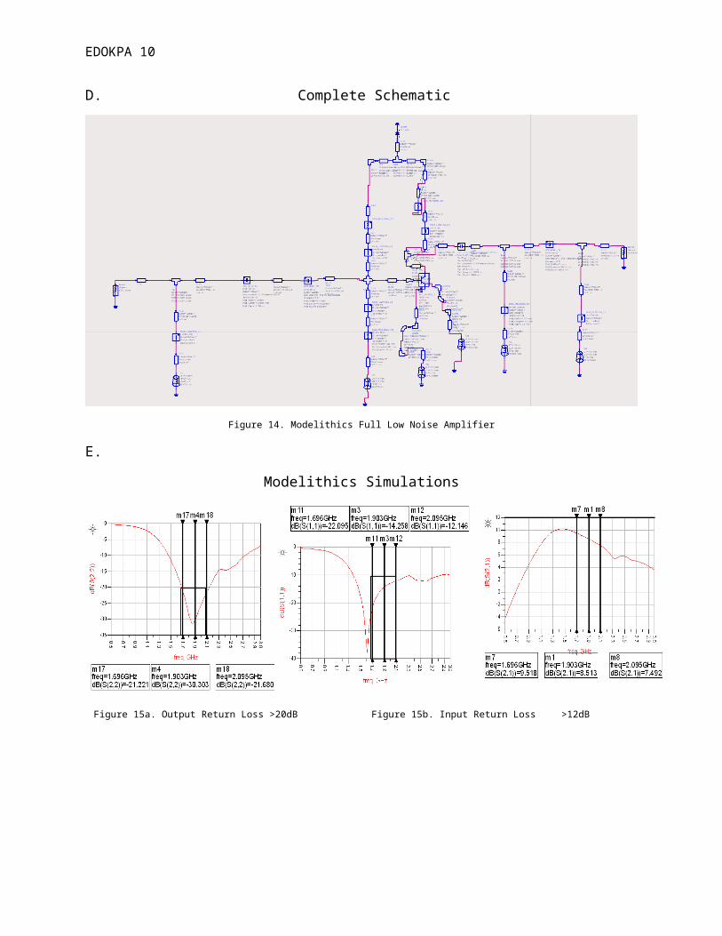
Figure 14. Modelithics Full Low Noise Amplifier
EDOKPA 9
E.
Modelithics Simulations
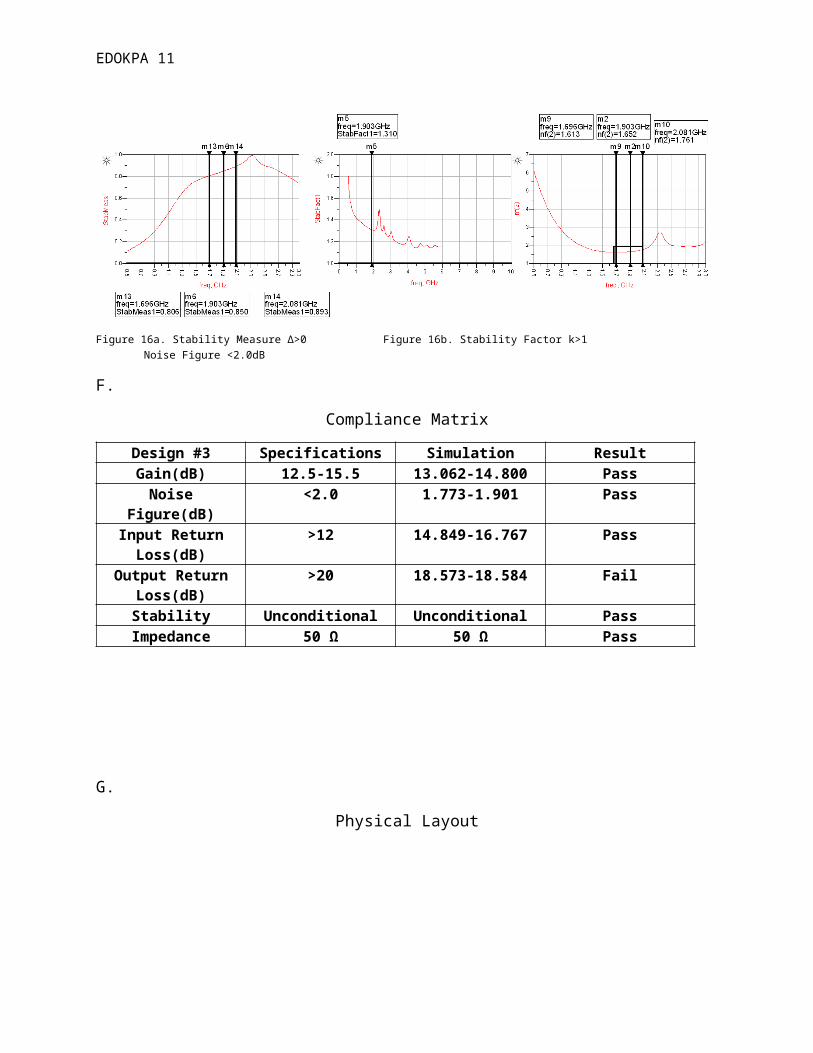
Figure 16a. Stability Measure ∆>0 Figure 16b. Stability Factor k>1 Noise Figure <2.0dB
F.
Compliance Matrix
Design #3 Specifications Simulation ResultGain(dB) 12.5-15.5 13.062-14.800 Pass
Noise Figure(dB) <2.0 1.773-1.901 PassInput Return Loss(dB) >12 14.849-16.767 Pass
Output Return Loss(dB)
>20 18.573-18.584 Fail
Stability Unconditional Unconditional PassImpedance 50 Ω 50 Ω Pass
Figure 15a. Output Return Loss >20dB Figure 15b. Input Return Loss >12dB Figure 15c. Gain <12.5dB
EDOKPA 10
G.
Physical Layout
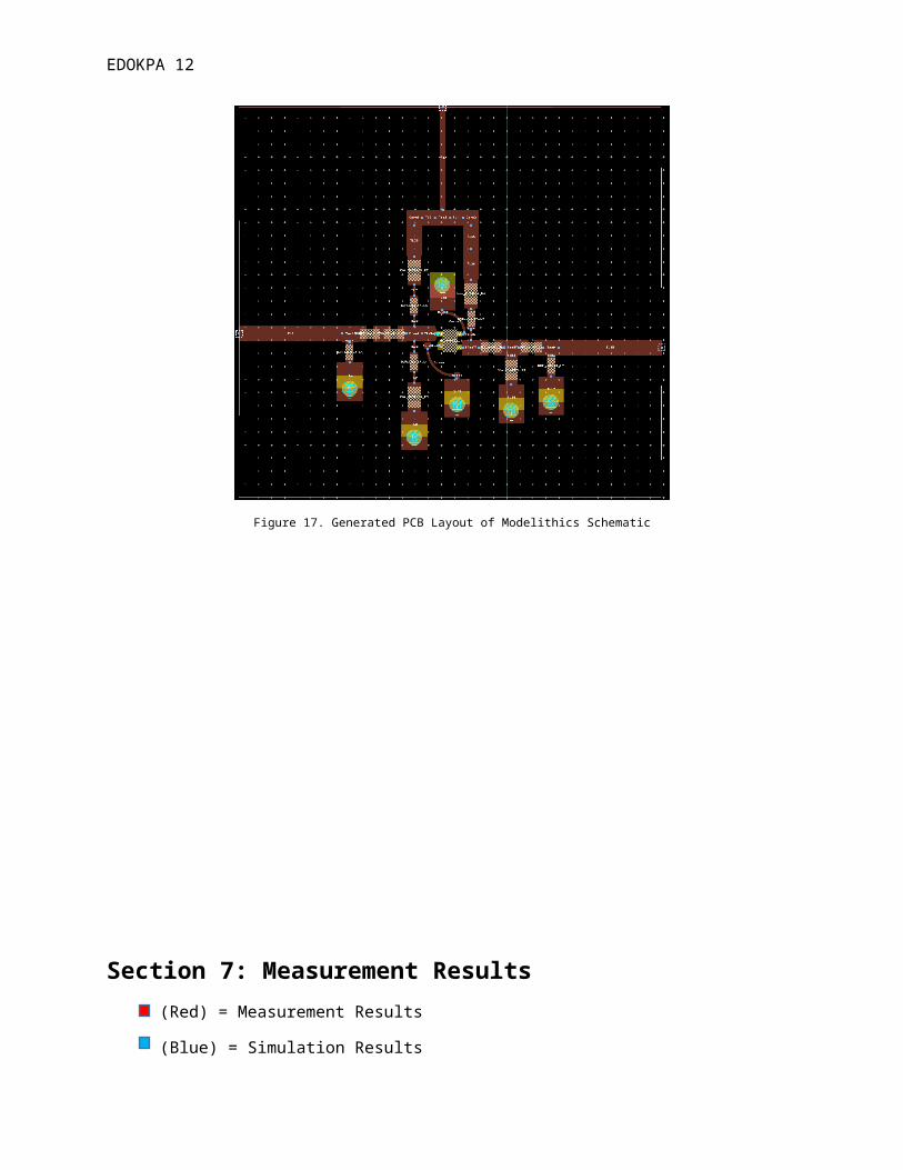
Figure 17. Generated PCB Layout of Modelithics Schematic
EDOKPA 11
Section 7: Measurement Results(Red) = Measurement Results
(Blue) = Simulation Results
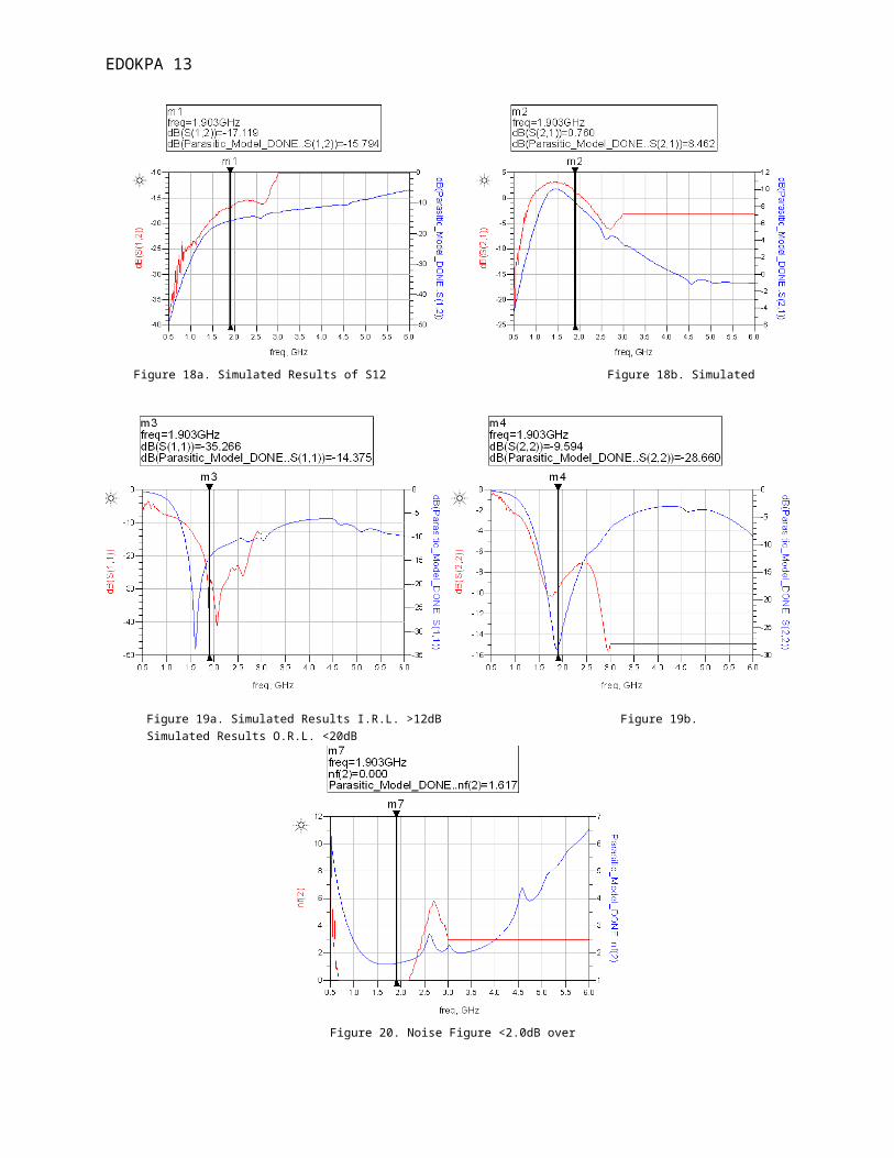
Figure 18a. Simulated Results of S12 Figure 18b. Simulated Results of <12.5dB
Figure 19a. Simulated Results I.R.L. >12dB Figure 19b. Simulated Results O.R.L. <20dB
EDOKPA 12
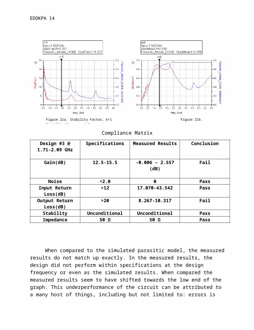
Compliance Matrix
Design #3 @1.71-2.09 GHz
Specifications Measured Results Conclusion
Gain(dB) 12.5-15.5 -0.006 – 2.557 (dB) Fail
Noise <2.0 0 PassInput Return Loss(dB) >12 17.070-43.542 Pass
Output Return Loss(dB) >20 8.267-10.317 Fail
Stability Unconditional Unconditional PassImpedance 50 Ω 50 Ω Pass
Figure 20. Noise Figure <2.0dB over Bandwidth
Figure 21a. Stability Factor, k>1 Figure 21b. Stability Measure, ∆>0
EDOKPA 13
When compared to the simulated parasitic model, the measured results do not match up exactly. In the measured results, the design did not perform within specifications at the design frequency or even as the simulated results. When compared the measured results seem to have shifted towards the low end of the graph. This underperformance of the circuit can be attributed to a many host of things, including but not limited to: errors is fabrication, errors in soldering, imperfections in components, and environmental conditions. The best way to account for these undesired effects is to tune the design by altering the characteristics of the transmission lines and the changing the value of the components.
Section 8: Summary
Throughout the design process of this low noise amplifier there were a few processes that could have been streamlined to save time. For example, in the design of the Modelithics model schematic and PCB layout, there were many times when the geometry and component values had to be tuned and adjusted in order to successfully operate. If the tuning had been saved until after the geometry of the PCB layout had been designed and then tuned returned to adjust the lines and component values that would have been more helpful in expediting the design process of the critical design factor.
With regards to the results of the fabricated printed circuit board, the results were unexpectedly good. The physical low noise amplifier was anticipated to be drastically different because of errors and non-idealities not accounted for by the Modelithics CLR components. Although the gain specification was never met in the simulations of the parasitic model or the measured results and with the additional failing of the output return loss of the measured results, the overall performance of the low noise amplifier was good. To improve performance of future design, a bias point located higher on the curve would indeed allow for more room to achieve specifications.
EDOKPA 14
Section 9: AppendixActive_Network_IDEAL - Schematic layout of ideal components of transistor network
Biasing - Schematic showing connection b/t ideal transistor and biasing values
BJT_Bias_Selection - *not important *
BJT_Bias_Selection.dds - *not important*
BJT_SP_NF_Match_Circ -ADS generated Transistor Network with modified resistor values
BJT_SP_NF_Match_Circ.dds - ADS simulation to choose bias point
DA_BJTBias1_biasing - Resistor Bias network with resulted from bias point selection
DA_BJTBias_biasing - *not important*
DA_SmithChartMatch1_IMN - Input matching network with discrete components and values
DA_SmithChartMatch_OMN - Output matching network with discrete components and values
IMN_Higher_level_schematic - High Level schematic of Input Matching Network
Input_Matching_IDEAL - Ideal input matching network with discrete components
LNA_IDEAL - Completed LNA with ideal components and discrete values
LNA_IDEAL.dds - Simulation results on LNA
LNA_REAL - Parasitic layout and schematic model of LNA with discrete values
LNA_REAL.dds - Simulation of parasitic schematic model
OMN_Higher_level_schematic - Higher level schematic of Output Matching Network
Output_Matching_IDEAL - Output matching network with ideal components and discrete values
TEST_IMN_IDEAL - High level ideal input matching network with terms for testing
TEST_IMN_IDEAL.dds - Results of testing of ideal input matching network
TEST_OMN_IDEAL - High level ideal output matching network with ports for testing
TEST_OMN_IDEAL.dds - Results of testing of ideal output matching network
TRAN_TEST_IDEAL - Testing of bias network
TRAN_TEST_IDEAL.dds - Simulation results of bias network testing