88x5113 datasheet - public - marvell technology group · marvell. moving forward faster doc. no....
TRANSCRIPT
Marvell. Moving Forward Faster
Doc. No. MV-S110852-U0, Rev. B
July 30, 2018
Document Classification: Public
88X5113Integrated 100G/40G/Quad 25 Gbps Ethernet PHY with Copper Cable and Backplane Drive Capability
Datasheet - Public
Cover

Document Conventions
Note: Provides related information or information of special importance.
Caution: Indicates potential damage to hardware or software, or loss of data.
Warning: Indicates a risk of personal injury.
For more information, visit our website at: www.marvell.com
DisclaimerTHIS DOCUMENT AND THE INFORMATION FURNISHED IN THIS DOCUMENT ARE PROVIDED “AS IS” WITHOUT ANY WARRANTY. MARVELL EXPRESSLY DISCLAIMS AND MAKES NO WARRANTIES OR GUARANTEES, WHETHER EXPRESS, ORAL, IMPLIED, STATUTORY, ARISING BY OPERATION OF LAW, OR AS A RESULT OF USAGE OF TRADE, COURSE OF DEALING, OR COURSE OF PERFORMANCE, INCLUDING THE IMPLIED WARRANTIES OF MERCHANTABILITY AND FITNESS FOR PARTICULAR PURPOSE AND NON-INFRINGEMENT.
This document, including any software or firmware included or referenced in this document is owned by Marvell. The information furnished in this document is provided for reference purposes only for use with Marvell products. It is the user's own responsibility to design or build products with the information. Marvell products are not authorized for use as critical components in medical devices, military systems, life or critical support devices, or related systems. Marvell is not liable, in whole or in part, and the user shall indemnify and hold Marvell harmless for any claim, damage, or other liability related to any such use of Marvell products. Marvell and the Marvell logo are registered trademarks of Marvell. For a more complete listing of Marvell trademarks, visit www.marvell.com.
Copyright © 2018. Marvell International Ltd. All rights reserved.
Doc. No. MV-S110852-U0 Rev. B Copyright © 2018 Marvell
Page 2 Document Classification: Public July 30, 2018
88X5113 Datasheet - Public

88X5113 Datasheet - PublicIntegrated 100G/40G/Quad 25 Gbps Ethernet PHY with Copper Cable and
Backplane Drive Capability
Copyright © 2018 Marvell Doc. No. MV-S110852-U0 Rev. B
July 30, 2018 Document Classification: Public Page 3
PRODUCT OVERVIEW
The Marvell® 88X5113 device is a fully integrated single chip Ethernet transceiver that supports 25 GbE full-duplex transmission, over a variety of media including optics, passive copper cables and backplanes.
The device operates as a single port 100 Gbps Ethernet PHY/Quad port 25 Gbps Ethernet PHY. In this mode, the 88X5113 100 GbE and 25 GbE transmission over a variety of media including optics, passive copper cables and backplanes.
The 88X5113 has long reach SERDES, and includes Auto-Negotiation and coefficient training functionality.
In the 100 Gbps and 25 Gbps Ethernet PHY modes, the 88X5113 connects to the MAC/Switch device over a CAUI-4 or 25GAUI interface respectively. On the host interface, the device also supports the IEEE 802.3 Clause 91 100G Reed Solomon Forward Error Correction (RS-FEC) as well as the IEEE 802.3 Clause 108 RS-FEC and IEEE 802.3 Clause 74 KR-FEC for 25 GbE operation. These along with the support for Auto-Negotiation and training protocol enable the device to interface with the MAC over a 100G-KR4/25G-KR backplane link.
The PHY mode, the line interface of the 88X5113, is fully compliant to the IEEE 802.3bj and IEEE 802.3bm standards for 100 GbE and IEEE 802.3by specifications for 25 GbE operation over passive copper cables, optics and backplanes. The device supports the IEEE 802.3 Clause 91 and IEEE 802.3 Clause 108 Reed Solomon Forward Error Correction (RS-FEC) features, IEEE 802.3 Clause 74 KR-FEC, and Auto-Negotiation and coefficient training protocol required by the IEEE 802.3bj and IEEE 802.3by standards.
Internal registers can be accessed via an MDIO/MDC serial management interface which is compliant with IEEE 802.3 specification Clause 45. An MDC frequency of up to 25 MHz supported.
The 88X5113 is manufactured in a 14 mm x 14 mm 169-pin FCBGA package.
Features Single port 100 GbE/Quad 25 GbE PHY
functionality Line equalization capability that meets IEEE 802.3bj
and 802.3by specifications 100G/40GBASE-KR4/25G-KR compliant Host
interface that exceed XLAUI/25GAUI requirements Fully autonomous adaptive equalization on line and
host receivers 3 tap transmit FIR with programmable level and
pre-emphasis Fully symmetric architecture with 100 GbE and
25 GbE RS-FEC and 10GE/25GE KR-FEC on both line and host interfaces
Auto-Negotiation for backplanes and cable assemblies as defined by IEEE 802.3 Clause 73 of IEEE 802.3
Support for transmit coefficient training protocol Clause 45 MDIO register access Ability to initialize the device from an external
EEPROM Hardware interrupt pin for hardware interrupt
generation capability LED pins with fully programmable event mapping
and solid/blink modes Packet and PRBS pattern generation/checking
capability Loopback mode for diagnostics Non-destructive eye monitors on all high speed
interfaces IEEE-1149.1 and 1149.6 JTAG support Operating temperature range up to 105°C Junction 14 mm x 14 mm 169-pin FCBGA package with 1mm
ball pitch
Applications 25 Gbps Ethernet NICs 100 Gbps/25 Gbps Ethernet line cards 100 Gbps/25 Gbps Ethernet backplanes

Doc. No. MV-S110852-U0 Rev. B Copyright © 2018 Marvell
Page 4 Document Classification: Public July 30, 2018
88X5113 Datasheet - Public
Figure 1: 88X5113 in a 25 GbE/100 GE Line Card Application
Figure 2: 88X5113 in a 25 GbE/100 GE Blade Switch/Server Application
100G/40G/40GbE/10G MAC/Switch
100GE – CAUI-440GE – XLAUI25GE – 25GAUI10GE - XFI
88X5113
100G – LR4, SR4, CR440G – LR4, SR4, CR425G – SR, CR10G – LR, SR, DAC
MAC Interface
Media Interface
100G/40GQSFP
4
100G/40G/40GbE/10G MAC/Switch
100GE – 100G-KR440GE – 40G-KR425GE – 25G-KR10GE – 10G-KR
88X5113
100G – LR4, SR4, CR440G – LR4, SR4, CR425G – SR, CR10G – LR, SR, DAC
MAC Interface
Media Interface
100G/40GQSFP
4
Backplane

Table of Contents
Copyright © 2018 Marvell Doc. No. MV-S110852-U0 Rev. B
July 30, 2018 Document Classification: Public Page 5
Table of Contents
Product Overview ......................................................................................................................................3
1 General Device Description ........................................................................................................... 13
2 Signal Description .......................................................................................................................... 15
2.1 Pin Map ............................................................................................................................................................... 16
2.2 Pin Description .................................................................................................................................................... 17
2.3 88X5113 Device Pin Assignment List ................................................................................................................. 23
3 Functional Description ................................................................................................................... 26
3.1 Data Path ............................................................................................................................................................ 263.1.1 PCS Mode ............................................................................................................................................ 27
3.2 Reset ................................................................................................................................................................... 28
3.3 Hardware Configuration ...................................................................................................................................... 30
3.4 Register Access .................................................................................................................................................. 313.4.1 IEEE MDC/MDIO Register Access ....................................................................................................... 313.4.2 TWSI Register Access .......................................................................................................................... 32
3.4.2.1 Bus Operation .................................................................................................................. 323.4.2.2 Clause 45 Encapsulation .................................................................................................. 33
3.5 TWSI, GPIO, and LED ........................................................................................................................................ 363.5.1 GPIO[3:0] and LED[3:0] ........................................................................................................................ 36
3.5.1.1 Controlling and Sensing ................................................................................................... 363.5.1.2 GPIO Interrupts ................................................................................................................ 363.5.1.3 LED .................................................................................................................................. 38
3.5.2 TWSI, GPIO 4, and GPIO 5 .................................................................................................................. 423.5.3 Two-wire Serial Interface (TWSI) ......................................................................................................... 46
3.6 Interrupt ............................................................................................................................................................... 46
3.7 Power Management ............................................................................................................................................ 53
3.8 IEEE 1149.1 and 1149.6 Controller .................................................................................................................... 543.8.1 BYPASS Instruction .............................................................................................................................. 543.8.2 SAMPLE/PRELOAD Instruction ........................................................................................................... 553.8.3 EXTEST Instruction .............................................................................................................................. 573.8.4 CLAMP Instruction ................................................................................................................................ 573.8.5 HIGH-Z Instruction ................................................................................................................................ 583.8.6 ID CODE Instruction ............................................................................................................................. 583.8.7 EXTEST_PULSE Instruction ................................................................................................................ 583.8.8 EXTEST_TRAIN Instruction ................................................................................................................. 58
3.9 Temperature Sensor ........................................................................................................................................... 59
3.10 On-chip Processor .............................................................................................................................................. 59
3.11 Synchronous Ethernet Mode .............................................................................................................................. 59
3.12 Power Supplies ................................................................................................................................................... 63

88X5113 Datasheet - Public
Doc. No. MV-S110852-U0 Rev. B Copyright © 2018 Marvell
Page 6 Document Classification: Public July 30, 2018
4 Line Side Description ..................................................................................................................... 64
4.1 Interface Modes of Operation ............................................................................................................................. 65
4.2 Electrical Interface .............................................................................................................................................. 72
4.3 PCS and PMA ..................................................................................................................................................... 724.3.1 100GBASE-R4 PCS (Modes P100*) .................................................................................................... 734.3.2 40GBASE-R4, 50GBASE-R4, 50GBASE-R2 PCS (Modes P40*, P50*) .............................................. 754.3.3 5GBASE-R, 10GBASE-R, and 25GBASE-R PCS (Modes P5L, P10*, P25*) ...................................... 774.3.4 SGMII, 1000BASE-X, and 2.5GBASE-X .............................................................................................. 78
4.3.4.1 PCS .................................................................................................................................. 784.3.4.2 1000BASE-X Auto-Negotiation ........................................................................................ 784.3.4.3 SGMII Auto-Negotiation ................................................................................................... 794.3.4.4 Auto-Negotiation Bypass Mode ........................................................................................ 79
4.4 Auto-Negotiation ................................................................................................................................................. 80
4.5 Loopback ............................................................................................................................................................ 814.5.1 Line-side Loopbacks ............................................................................................................................. 814.5.2 Host-side Loopbacks ............................................................................................................................ 82
4.6 Synchronized FIFO ............................................................................................................................................. 84
4.7 Traffic Generation and Checking ........................................................................................................................ 844.7.1 Packet Generator ................................................................................................................................. 864.7.2 Packet Checker .................................................................................................................................... 90
4.8 PRBS Generation and Checking ........................................................................................................................ 914.8.1 General PRBS Generators and Checkers ............................................................................................ 914.8.2 40GBASE-R4-specific Generators and Checkers ................................................................................ 934.8.3 100GBASE-R4-specific Generators and Checkers .............................................................................. 93
4.9 Eye Monitor ......................................................................................................................................................... 93
5 Host Side Description .................................................................................................................... 94
6 Chip Bring Up .................................................................................................................................. 99
6.1 Power Sequencing .............................................................................................................................................. 99
6.2 Reset and Configuration ..................................................................................................................................... 99
7 Electrical Specifications .............................................................................................................. 100
7.1 Absolute Maximum Ratings .............................................................................................................................. 100
7.2 Recommended Operating Conditions ............................................................................................................... 101
7.3 Package Thermal Information ........................................................................................................................... 1027.3.1 Thermal Conditions for 169-pin, FCBGA Package ............................................................................. 102
7.4 Current Consumption ........................................................................................................................................ 1037.4.1 88X5113 Current Consumption (Commercial) ................................................................................... 1037.4.2 88X5113 Current Consumption (Industrial) ........................................................................................ 105
7.5 Digital I/O Electrical Specifications ................................................................................................................... 1077.5.1 DC Operating Conditions .................................................................................................................... 1077.5.2 AC Operating Conditions .................................................................................................................... 1087.5.3 Reset Timing ...................................................................................................................................... 1087.5.4 MDC/MDIO Management Interface Timing ........................................................................................ 1097.5.5 JTAG Timing ....................................................................................................................................... 110
7.6 SERDES Electrical Specifications .................................................................................................................... 1117.6.1 Chip-to-Module 100 Gbps/25 Gbps Electrical Characteristics ........................................................... 111
7.6.1.1 Chip-to-Module 100 Gbps/25 Gbps Transmitter and Receiver Characteristics .............. 111

Table of Contents
Copyright © 2018 Marvell Doc. No. MV-S110852-U0 Rev. B
July 30, 2018 Document Classification: Public Page 7
7.6.1.2 Chip-to-Module CAUI-4/XXVAUI-1 Interface Transmitter Output Voltage Limits and Definitions .......................................................................................................................113
7.6.2 Chip-to-Chip 100 Gbps/25 Gbps (CAUI-4/XXVAUI-1) Electrical Characteristics ............................... 1157.6.2.1 Chip-to-Chip 100 Gbps/25 Gbps (CAUI-4/XXVAUI-1) Transmitter and Receiver
Characteristics ................................................................................................................1157.6.2.2 Chip-to-Chip CAUI-4/XXVAUI-1 Interface Transmitter Output Voltage Limits and
Definitions .......................................................................................................................1177.6.3 100GBASE-CR4/50GBASE-CR2/25GBASE-CR Electrical Characteristics ....................................... 119
7.6.3.1 100GBASE-CR4/50GBASE-CR2/25GBASE-CR Interface Transmitter and Receiver Characteristics ................................................................................................................119
7.6.3.2 100GBASE-CR4/50GBASE-CR2/25GBASE-CR Interface Transmitter Output Voltage Limits and Definitions .....................................................................................................122
7.6.4 100GBASE-KR4/50GBASE-KR2/25GBASE-KR Electrical Characteristics ....................................... 1237.6.4.1 100GBASE-KR4/50GBASE-KR2/25GBASE-KR Interface Transmitter and Receiver
Characteristics ................................................................................................................1237.6.4.2 100GBASE-KR4/50GBASE-KR2/25GBASE-KR Interface Transmitter Output Voltage
Limits and Definitions .....................................................................................................1267.6.5 40 Gbps Parallel Physical Interface (XLPPI) Electrical Characteristics .............................................. 127
7.6.5.1 40 Gbps Parallel Physical Interface (XLPPI) Interface Transmitter and Receiver Characteristics ................................................................................................................127
7.6.5.2 XLPPI Interface Transmitter Output Voltage Limits and Definitions ............................... 1297.6.6 40 Gbps Attachment Unit Interface (XLAUI) Electrical Characteristics .............................................. 131
7.6.6.1 40 Gbps Attachment Unit Interface (XLAUI) Interface Transmitter and Receiver Characteristics ................................................................................................................131
7.6.6.2 XLAUI Interface Transmitter Output Voltage Limits and Definitions ............................... 1347.6.7 40GBASE-CR4 Electrical Characteristics .......................................................................................... 135
7.6.7.1 40GBASE-CR4 Interface Transmitter and Receiver Characteristics .............................. 1357.6.7.2 40GBASE-CR4 Interface Transmitter Output Voltage Limits and Definitions ................ 137
7.6.8 40GBASE-KR4 Electrical Characteristics ........................................................................................... 1387.6.8.1 40GBASE-KR4 Interface Transmitter and Receiver Characteristics .............................. 1387.6.8.2 40GBASE-KR4 Interface Transmitter Output Voltage Limits and Definitions ................. 140
7.6.9 SFP+ Interface (SFI) Limiting Module Electrical Characteristics ........................................................ 1427.6.9.1 SFI Transmitter and Receiver Characteristics ............................................................... 1427.6.9.2 SFP+ Direct Attach Cable (10GSFP+CU Appendix E) Transmitter and Receiver
Characteristics ................................................................................................................1447.6.10 10 Gigabit Small Form Factor Pluggable Interface (XFI) Electrical Characteristics ........................... 148
7.6.10.1 XFI Interface Transmitter and Receiver Characteristics ................................................. 1487.6.11 10GBASE-KR Electrical Characteristics ............................................................................................. 150
7.6.11.1 10GBASE-KR Interface Transmitter and Receiver Characteristics ................................ 1507.6.11.2 10GBASE-KR Interface Transmitter Output Voltage Limits and Definitions ................... 152
7.7 Reference Clock ............................................................................................................................................... 153
7.8 Output 25 MHz Clock ........................................................................................................................................ 154
7.9 Latency ............................................................................................................................................................. 155
8 Mechanical Drawings ................................................................................................................... 156
8.1 Package Mechanical Drawings ......................................................................................................................... 156
9 Order Information ......................................................................................................................... 159
9.1 Ordering Part Numbers and Package Markings ............................................................................................... 1599.1.1 Marking Example ................................................................................................................................ 160
A Revision History ........................................................................................................................... 161

88X5113 Datasheet - Public
Doc. No. MV-S110852-U0 Rev. B Copyright © 2018 Marvell
Page 8 Document Classification: Public July 30, 2018
List of Figures
Product Overview .......................................................................................................................................3
Figure 1: 88X5113 in a 25 GbE/100 GE Line Card Application .........................................................................4
Figure 2: 88X5113 in a 25 GbE/100 GE Blade Switch/Server Application ........................................................4
1 General Device Description .............................................................................................................13
Figure 3: 88X5113 Device Functional Block Diagram .....................................................................................14
2 Signal Description ............................................................................................................................15
3 Functional Description.....................................................................................................................26
Figure 4: 88X5113 Main Operational Modes ..................................................................................................26
Figure 5: Typical MDC/MDIO Read Operation ...............................................................................................31
Figure 6: Typical MDC/MDIO Write Operation.................................................................................................31
Figure 7: First Two Bytes of All Transactions ..................................................................................................33
Figure 8: Write, Full Header, Retain REGAD...................................................................................................34
Figure 9: Write, Full Header, Post-Increment ..................................................................................................34
Figure 10: Write, Abbreviated Header, Retain REGAD .....................................................................................35
Figure 11: Write, Abbreviated Header, Post-Increment .....................................................................................35
Figure 12: Read, Full Header, Retain REGAD ..................................................................................................35
Figure 13: Read, Full Header, Post-Increment ..................................................................................................35
Figure 14: Read, Abbreviated Header, Retain REGAD .....................................................................................35
Figure 15: Read, Abbreviated Header, Post-Increment .....................................................................................35
Figure 16: Dummy Write Command to Set REGAD ..........................................................................................35
Figure 17: LED Chain ........................................................................................................................................38
Figure 18: Various LED Hookup Configurations ................................................................................................39
Figure 19: Interrupt Hierarchy and Aggregation from Different Blocks ..............................................................47
Figure 20: Synchronous Ethernet with 88X5113 in a Non-Ethernet Application such as CPRI.........................60
Figure 21: Synchronous Ethernet with 88X5113 in an Ethernet Application .....................................................61
Figure 22: Multiplexing Scheme for Recovered Clock RCLKA ..........................................................................62
4 Line Side Description .......................................................................................................................64
Figure 23: 100GBASE-R4 Data Path.................................................................................................................74
Figure 24: 40GBASE-R4, 50GBASE-R4, and 50GBASE-R2 Datapath.............................................................76
Figure 25: 5GBASE-R, 10GBASE-R, and 25GBASE-R Datapath.....................................................................78
Figure 26: Line-side Loopback...........................................................................................................................81
Figure 27: Turn On Deep Host Loopback ..........................................................................................................82
Figure 28: Packet Format ..................................................................................................................................86
Figure 29: Normal CRC Calculation (in XLGMII/40G and CGMII/100G Format) ...............................................87
Figure 30: Extended CRC Calculation (in XLGMII/40G and CGMII/100G Format) ...........................................87
Figure 31: Packet without CRC (in XLGMII/40G and CGMII/100G Format) ......................................................88

List of Figures
Copyright © 2018 Marvell Doc. No. MV-S110852-U0 Rev. B
July 30, 2018 Document Classification: Public Page 9
5 Host Side Description ......................................................................................................................94
6 Chip Bring Up....................................................................................................................................99
7 Electrical Specifications ................................................................................................................100
Figure 32: Reset Timing...................................................................................................................................108
Figure 33: MDC/MDIO Management Interface ................................................................................................109
Figure 34: JTAG Timing...................................................................................................................................110
Figure 35: Chip-to-Module CAUI-4/XXVAUI-1 Interface Transmitter Output Voltage Limits and Definitions...113
Figure 36: Chip-to-Module CAUI-4/XXVAUI-1 Transmitter Output Differential Amplitude and Eye Opening ..114
Figure 37: Chip-to-Chip CAUI-4/XXVAUI-1 Interface Transmitter Output Voltage Limits and Definitions ......117
Figure 38: Chip-to-Chip CAUI-4/XXVAUI-1 Transmitter Output Differential Amplitude and Eye Opening.......118
Figure 39: 100GBASE-CR4/50GBASE-CR2/25GBASE-CR Interface Transmitter Output Voltage Limits and Definitions ................................................................................................................................122
Figure 40: 100GBASE-KR4/50GBASE-KR2/25GBASE-KR Interface Transmitter Output Voltage Limits and Definitions .......................................................................................................................................126
Figure 41: XLPPI Interface Transmitter Output Voltage Limits and Definitions ...............................................129
Figure 42: XLPPI Transmitter Output Differential Amplitude and Eye Opening...............................................130
Figure 43: XLAUI Interface Transmitter Output Voltage Limits and Definitions ...............................................134
Figure 44: XLAUI Transmitter Output Differential Amplitude and Eye Opening...............................................134
Figure 45: 40GBASE-CR4Interface Transmitter Output Voltage Limits and Definitions..................................137
Figure 46: 40GBASE-CR4Transmitter Output Differential Amplitude and Eye Opening .................................137
Figure 47: 40GBASE-KR4 Interface Transmitter Output Voltage Limits and Definitions.................................140
Figure 48: 40GBASE-KR4 Transmitter Output Differential Amplitude and Eye Opening ................................141
Figure 49: SFI Transmitter Output Voltage Limits and Definitions...................................................................146
Figure 50: SFI Transmitter Output Differential Amplitude and Eye Opening ...................................................147
Figure 51: 10GBASE-KR Interface Transmitter Output Voltage Limits and Definitions...................................152
Figure 52: 10GBASE-KR Transmitter Output Differential Amplitude and Eye Opening ..................................152
Figure 53: Reference Clock Input Waveform...................................................................................................153
8 Mechanical Drawings .....................................................................................................................156
Figure 54: 169-pin FCBGA 14 × 14 Package Mechanical Drawings — Top and Side View ...........................156
Figure 55: 169-pin FCBGA 14 × 14 Package Mechanical Drawings — Bottom View .....................................157
9 Order Information ...........................................................................................................................159
Figure 56: Sample Part Number ......................................................................................................................159
Figure 57: 88X5113 169-pin FCBGA Commercial Green Package Marking and Pin 1 Location ....................160
Figure 58: 88X5113 169-pin FCBGA Industrial Green Package Marking and Pin 1 Location.........................160
A Revision History .............................................................................................................................161

88X5113 Datasheet - Public
Doc. No. MV-S110852-U0 Rev. B Copyright © 2018 Marvell
Page 10 Document Classification: Public July 30, 2018
List of Tables
Product Overview .......................................................................................................................................3
1 General Device Description .............................................................................................................13
2 Signal Description ............................................................................................................................15
Table 1: Pin Type Definitions..........................................................................................................................15
Table 2: Line Side Interface............................................................................................................................17
Table 3: Host Side Interface ...........................................................................................................................17
Table 4: Clocking and Reference ...................................................................................................................18
Table 5: Configuration and Reset ...................................................................................................................18
Table 6: Management Interface......................................................................................................................18
Table 7: EEPROM/GPIO ................................................................................................................................18
Table 8: JTAG.................................................................................................................................................19
Table 9: GPIO/LED.........................................................................................................................................19
Table 10: TEST.................................................................................................................................................19
Table 11: Power and Ground............................................................................................................................20
Table 12: 88X5113 Pin List — Alphabetical by Signal Name ...........................................................................23
3 Functional Description.....................................................................................................................26
Table 13: Valid PCS Mode Interface Connections ...........................................................................................27
Table 14: Reset Bits .........................................................................................................................................28
Table 15: Hardware Configuration....................................................................................................................30
Table 16: Extensions for Management Frame Format for Indirect Access.......................................................31
Table 17: INS[2:0] Definition.............................................................................................................................33
Table 18: GPIO, LED Signal Mapping ..............................................................................................................36
Table 19: GPIO/LED Controls ..........................................................................................................................37
Table 20: LED[3:0] Control and Status Register Bits........................................................................................39
Table 21: LED Timer Control ............................................................................................................................40
Table 22: TWSI and GPIO Signal Mapping ......................................................................................................42
Table 23: SCL Control ......................................................................................................................................42
Table 24: SDA Control ......................................................................................................................................43
Table 25: I/O Open Drain Control .....................................................................................................................45
Table 26: Global Interrupt Control ....................................................................................................................46
Table 27: Global Interrupt Status......................................................................................................................47
Table 28: 1G/2.5G Interrupt Enable, Interrupt Status, and Real-Time Status ..................................................48
Table 29: 10G/25G Interrupt Enable, Interrupt Status, and Real-Time Status .................................................48
Table 30: 40G/50G Interrupt Enable, Interrupt Status, and Real-Time Status .................................................49
Table 31: 100G Interrupt Enable, Interrupt Status, and Real-Time Status .......................................................49
Table 32: Excessive Link Error Interrupt Enable, Interrupt Status, and Real-Time Status ...............................50
Table 33: GPIO1, GPIO2, GPIO3, GPIO4, CLK_OUT_SE1, CLK_OUT_SE2 Pins Interrupt...........................51
List of Tables
Copyright © 2018 Marvell Doc. No. MV-S110852-U0 Rev. B
July 30, 2018 Document Classification: Public Page 11
Table 34: Temp Sensor and GPIOs, Interrupt Enable, Interrupt Status ...........................................................51
Table 35: Power Down Control Bits..................................................................................................................53
Table 36: TAP Controller Opcodes...................................................................................................................54
Table 37: Boundary Scan Chain Order.............................................................................................................55
Table 38: ID CODE Instruction .........................................................................................................................58
4 Line Side Description .......................................................................................................................64
Table 39: Mode Definition Reference ...............................................................................................................65
Table 40: Interface Modes of Operation ...........................................................................................................66
Table 41: Register Control to Select Mode of Operation ..................................................................................69
Table 42: Base Link Register on PCS Modes ..................................................................................................71
Table 43: PCS Types........................................................................................................................................72
Table 44: SGMII Auto-Negotiation Modes ........................................................................................................79
Table 45: Shallow Line Loopback Control Bits .................................................................................................81
Table 46: Deep Loopback Control Bits .............................................................................................................82
Table 47: Shallow Line Loopback Control Bits .................................................................................................83
Table 48: Deep Loopback Control Bits .............................................................................................................83
Table 49: Packet Generator and Checker Register Mapping Data ..................................................................84
Table 50: Packet Generator and Checker Control and Counters .....................................................................85
Table 51: Registers Controlling Packet Generation..........................................................................................87
Table 52: IPG Configuration .............................................................................................................................88
Table 53: Packet Data Generation ...................................................................................................................89
Table 54: Registers Controlling Packet Checker ..............................................................................................90
Table 55: PRBS Register Address Offsets .......................................................................................................91
Table 56: Supported Line-side PRBS Patterns ................................................................................................92
Table 57: IEEE PCS and PMA PRBS Control Register....................................................................................93
5 Host Side Description ......................................................................................................................94
Table 58: Equivalent Registers Between Line and Host Interface....................................................................94
Table 59: Non-Reversible Mode Combinations ................................................................................................98
6 Chip Bring Up....................................................................................................................................99
7 Electrical Specifications ................................................................................................................100
Table 60: Absolute Maximum Ratings ............................................................................................................100
Table 61: Recommended Operating Conditions (Commercial) ......................................................................101
Table 62: Thermal Conditions for 169-pin, FCBGA Package .........................................................................102
Table 63: DVDD Current Consumption ..........................................................................................................103
Table 64: AVDDL and AVDDH Current Consumption ....................................................................................104
Table 65: AVDDC and AVDDT Current Consumption....................................................................................104
Table 66: DVDD Current Consumption ..........................................................................................................105
Table 67: AVDDL and AVDDH Current Consumption ....................................................................................106
Table 68: AVDDC and AVDDT Current Consumption....................................................................................107
Table 69: DC Operating Conditions................................................................................................................107
Table 70: AC Operating Conditions ................................................................................................................108

88X5113 Datasheet - Public
Doc. No. MV-S110852-U0 Rev. B Copyright © 2018 Marvell
Page 12 Document Classification: Public July 30, 2018
Table 71: Reset Timing...................................................................................................................................108
Table 72: MDC/MDIO Management Interface Timing.....................................................................................109
Table 73: JTAG Timing...................................................................................................................................110
Table 74: Chip-to-Module CAUI-4/XXVAUI-1 Transmitter and Receiver Characteristics ...............................111
Table 75: Chip-to-Module CAUI-4/XXVAUI-1 Settings and Configuration......................................................112
Table 76: Chip-to-Chip Gbps CAUI-4/XXVAUI-1 Interface Transmitter and Receiver Characteristics...........115
Table 77: Chip-to-Chip CAUI-4/XXVAUI-1 Settings and Configuration ..........................................................116
Table 78: 100GBASE-CR4/50GBASE-CR2/25GBASE-CR Interface Transmitter and Receiver Characteristics ................................................................................................................................119
Table 79: 100GBASE-CR4/50GBASE-CR2/25GBASE-CR Settings and Configuration ................................121
Table 80: 100GBASE-KR4/50GBASE-KR2/25GBASE-KR Interface Transmitter and Receiver Characteristics ................................................................................................................................123
Table 81: 100GBASE-KR4/50GBASE-KR2/25GBASE-KR Settings and Configuration.................................125
Table 82: XLPPI Interface Transmitter and Receiver Characteristics.............................................................127
Table 83: XLPPI Settings and Configuration ..................................................................................................129
Table 84: XLAUI Interface Transmitter and Receiver Characteristics ............................................................131
Table 85: XLAUI Settings and Configuration ..................................................................................................133
Table 86: 40GBASE-CR4 Interface Transmitter and Receiver Characteristics ..............................................135
Table 87: 40GBASE-CR4 Settings and Configuration....................................................................................136
Table 88: 40GBASE-KR4 Interface Transmitter and Receiver Characteristics ..............................................138
Table 89: 40GBASE-KR4 Settings and Configuration....................................................................................139
Table 90: SFI Transmitter and Receiver Characteristics ................................................................................142
Table 91: SFI Settings and Configuration.......................................................................................................143
Table 92: 10GSFP+CU Transmitter and Receiver Characteristics.................................................................144
Table 93: 10GSFP+CU Settings and Configuration .......................................................................................146
Table 94: XFI Interface Transmitter and Receiver Characteristics .................................................................148
Table 95: 10GBASE-KR Interface Transmitter and Receiver Characteristics ................................................150
Table 96: 10GBASE-KR Settings and Configuration......................................................................................151
Table 97: Reference Clock .............................................................................................................................153
Table 98: Output 25 MHz Clock......................................................................................................................154
Table 99: Chip Pin-to-pin Latency (Rx + Tx)...................................................................................................155
8 Mechanical Drawings .....................................................................................................................156
Table 100: 169-pin FCBGA (14 mm × 14 mm) Package Dimensions ..............................................................158
9 Order Information ...........................................................................................................................159
Table 101: 88X5113 Part Order Option ............................................................................................................159
A Revision History .............................................................................................................................161
Table 102: Revision History ..............................................................................................................................161

General Device Description
Copyright © 2018 Marvell Doc. No. MV-S110852-U0 Rev. B
July 30, 2018 Document Classification: Public Page 13
1 General Device Description
The 88X5113 device is an Ethernet SERDES Transceiver that supports one port of 100GBASE-R4, consortium 50GBASE-R2, overclocked 40GBASE-R2, 40GBASE-R4, and four ports of 25GBASE-R, consortium 25GBASE-R, 10GBASE-R, 5GBASE-R, 2.5GBASE-X, 1000BASE-X, and SGMII on both the line and host interfaces. Auto-Negotiation, equalization and KR training are available to support backplane, twin-ax, and optical options in the various modes. Reed Solomon FEC and KR-FEC can be enabled as well. The various CAUI-4, XLPPI, XLAUI, SFI, XFI interfaces are supported.
The device can be used in PCS mode application where data is passed from one PCS to another PCS.
Device registers can be accessed through standard Clause 45 MDC/MDIO. The device operates from a 0.9V/0.95V (I-temp operation) digital core voltage and a 1.0V analog voltage. The digital I/O signals can operate at 3.3V, 2.5V, 1.8V, 1.5V, 1.2V, and 1.05V. The device utilizes a 14 mm x 14 mm 169-ball FCBGA package, and supports an operating junction temperature of up to105°C.

88X5113 Datasheet - Public
Doc. No. MV-S110852-U0 Rev. B Copyright © 2018 Marvell
Page 14 Document Classification: Public July 30, 2018
Figure 3: 88X5113 Device Functional Block Diagram
Host Interface
(Same design as Line Side)
FIFO
SERDESLine lane 0
SERDESLine lane 1
SERDESLine lane 2
SERDESLine lane 3
Auto-NegPort 0/Multilane
Auto-NegPort 1/Lane 1
Auto-NegPort 2/Lane 2
Auto-NegPort 3/Lane 3
KR TrainingLane 0
KR TrainingLane 1
KR TrainingLane 2
KR TrainingLane 3
Reed Solomon FEC 100G/50G Sub-Port 0
RS-FEC 25GSub-Port 0
RS-FEC 25GSub-Port 1
RS-FEC 25GSub-Port 2
RS-FEC 25GSub-Port 3
KR-FEC 50G/40G Sub-Port 0 25G/10G Sub-Port 0
KR-FEC 50G/40G Sub-Port 0 25G/10G Sub-Port 1
KR-FEC 50G/40G Sub-Port 0 25G/10G Sub-Port 2
KR-FEC 50G/40G Port 0 25G/10G Port 3
100GBASE-R4 PCS Sub-Port 0
40/50GBASE-R4, 50GBASE-R2 PCS Sub-Port 0
5/10/25GBASE-R PCS Sub-Port 0
5/10/25GBASE-R PCS Sub-Port 1
5/10/25GBASE-R PCS Sub-Port 2
5/10/25GBASE-R PCS Sub-Port 3
1000/2.5GBASE-X SGMII Sub-Port 0
1000/2.5GBASE-X SGMII Sub-Port 1
1000/2.5GBASE-X SGMII Sub-Port 2
1000/2.5GBASE-X SGMII Sub-Port 3
Line Interface
LIP/N[0] LOP/N[0] LIP/N[1] LOP/N[1] LIP/N[2] LOP/N[2] LIP/N[3] LOP/N[3]
HOP/N[0] HOP/N[1] HOP/N[2] HOP/N[3]HIP/N[0] HIP/N[1] HIP/N[2] HIP/N[3]
ClockCLKP/N
CLK25P/N
Config/ Reset
CONFIG[2:0]
PHYAD[3:0]
RESETn
Register/Interrupt
MDIO
MDC
INTn
EEPROMSDA
SCL
LED/GPIO GPIO[3:0]
JTAG
TCK
TRSTn
TMS
TDI
TDO
TestTEST[1:0]
ATP
Power
DVDD
AVDDH
AVDDL
AVDDC
AVDDT
VDDON
VDDOS
VSEL_N
VSEL_S
AVSS
VSS

Signal Description
Copyright © 2018 Marvell Doc. No. MV-S110852-U0 Rev. B
July 30, 2018 Document Classification: Public Page 15
2 Signal Description
Table 1: Pin Type Definitions
Pin Type Definit ion
H Input with hysteresis
I/O Input and output
I Input only
O Output only
PU Internal pull-up
PD Internal pull-down
OD Open drain output
Z Tri-state output
mA DC sink capability
AI Analog input
AO Analog output
DI Digital input
DO Digital output
88X5113 Datasheet - Public
Doc. No. MV-S110852-U0 Rev. B Copyright © 2018 Marvell
Page 16 Document Classification: Public July 30, 2018
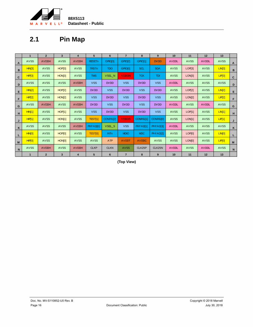
2.1 Pin Map
(Top View)
1 2 3 4 5 6 7 8 9 10 11 12 13
AAVSS AVDDH AVSS AVDDH RESETn GPIO[3] GPIO[2] GPIO[1] DVDD AVDDL AVSS AVDDL AVSS
A
BHIN[3] AVSS HOP[3] AVSS TRSTn TDO GPIO[0] SCL SDA AVSS LOP[3] AVSS LIN[3]
B
CHIP[3] AVSS HON[3] AVSS TMS VSEL_N VDDON TCK TDI AVSS LON[3] AVSS LIP[3]
C
DAVSS AVSS AVSS AVDDH VSS DVDD VSS DVDD VSS AVDDL AVSS AVSS AVSS
D
EHIN[2] AVSS HOP[2] AVSS DVDD VSS DVDD VSS DVDD AVSS LOP[2] AVSS LIN[2]
E
FHIP[2] AVSS HON[2] AVSS VSS DVDD VSS DVDD VSS AVSS LON[2] AVSS LIP[2]
F
GAVSS AVDDH AVSS AVDDH DVDD VSS DVDD VSS DVDD AVDDL AVSS AVDDL AVSS
G
HHIN[1] AVSS HOP[1] AVSS VSS DVDD VSS DVDD VSS AVSS LOP[1] AVSS LIN[1]
H
JHIP[1] AVSS HON[1] AVSS TEST[1] CONFIG[2] VDDOS CONFIG[1] CONFIG[0] AVSS LON[1] AVSS LIP[1]
J
KAVSS AVSS AVSS AVDDH PHYAD[0] VSEL_S VSS PHYAD[1] PHYAD[3] AVDDL AVSS AVSS AVSS
K
LHIN[0] AVSS HOP[0] AVSS TEST[0] INTn MDIO MDC PHYAD[2] AVSS LOP[0] AVSS LIN[0]
L
MHIP[0] AVSS HON[0] AVSS AVSS ATP AVDDT AVDDC AVSS AVSS LON[0] AVSS LIP[0]
M
NAVSS AVDDH AVSS AVDDH CLKP CLKN AVSS CLK25P CLK25N AVDDL AVSS AVDDL AVSS
N
1 2 3 4 5 6 7 8 9 10 11 12 13

Signal DescriptionPin Description
Copyright © 2018 Marvell Doc. No. MV-S110852-U0 Rev. B
July 30, 2018 Document Classification: Public Page 17
2.2 Pin Description
Table 2: Line Side Interface
Pin # Pin Name Pin Type
Description
C13F13J13M13
LIP[3]LIP[2]LIP[1]LIP[0]
AI Line Input Positive
B13E13H13L13
LIN[3]LIN[2]LIN[1]LIN[0]
AI Line Input Negative
B11E11H11L11
LOP[3]LOP[2]LOP[1]LOP[0]
AO Line Output Positive
C11F11J11M11
LON[3]LON[2]LON[1]LON[0]
AO Line Output Negative
Table 3: Host Side Interface
Pin # Pin Name Pin Type
Description
C1F1J1M1
HIP[3]HIP[2]HIP[1]HIP[0]
AI Host Input Positive
B1E1H1L1
HIN[3]HIN[2]HIN[1]HIN[0]
AI Host Input Negative
B3E3H3L3
HOP[3]HOP[2]HOP[1]HOP[0]
AO Host Output Positive
C3F3J3M3
HON[3]HON[2]HON[1]HON[0]
AO Host Output Negative
Note
The SERDES receiver is AC coupled on-chip. There is no off-chip AC-coupling capacitor required as long as the Rx input common mode is between AGND and AVDD (1.0V) and Rx amplitude is less than 1200 mVpp differential.

88X5113 Datasheet - Public
Doc. No. MV-S110852-U0 Rev. B Copyright © 2018 Marvell
Page 18 Document Classification: Public July 30, 2018
Table 4: Clocking and Reference
Pin # Pin Name Pin Type
Description
N5 CLKP AI Reference Clock Positive. Refer to Section 7.7 for further details.
N6 CLKN AI Reference Clock Negative. Refer to Section 7.7 for further details.
N8 CLK25P AO 25 MHz Clock Output Positive. Refer to Section 7.8 for further details.
N9 CLK25N AO 25 MHz Clock Output Negative. Refer to Section 7.8 for further details.
Table 5: Configuration and Reset
Pin # Pin Name Pin Type
Description
K9L9K8K5
PHYAD[3]PHYAD[2]PHYAD[1]PHYAD[0]
DI/PD
AddressIn MDIO mode, this sets the PHYAD[3:0] setting. PHYAD[4] is set to 0.In TWSI mode, this sets the A[3:0] setting. A[6:4] is set to 100.
J6J8J9
CONFIG[2]CONFIG[1]CONFIG[0]
DI/PD CONFIG[0] - 0 = MDIO 1 = TWSI
CONFIG[1] - 0 = Do not load EEPROM1 = Load EEPROM
CONFIG[2] - Reserved
A5 RESETn DI Hardware Reset, 0 = Reset1 = Normal operation
Table 6: Management Interface
Pin # Pin Name Pin Type
Description
L8 MDC/SSCL DI Management Interface Clock, or SCL for TWSI slave modeSee Section 3.4.1, IEEE MDC/MDIO Register Access for details.
L7 MDIO/SSDA IO,OD Management Interface Data, or SDA for TWSI slave modeSee Section 3.4.1, IEEE MDC/MDIO Register Access for details.This pin can be open drain.
L6 INTn OD Interrupt.
Table 7: EEPROM/GPIO
Pin # Pin Name Pin Type
Descript ion
B8 SCL IO, OD Multi-function pin for EEPROM Clock, or GPIO[4]. Primary function is Two Wire Serial Interface Clock, EEPROM Clock.
B9 SDA IO, OD Multi-function pin for EEPROM Data, or GPIO[5]. Primary function is Two Wire Serial Interface Data, EEPROM Data.

Signal DescriptionPin Description
Copyright © 2018 Marvell Doc. No. MV-S110852-U0 Rev. B
July 30, 2018 Document Classification: Public Page 19
Table 8: JTAG
Pin # Pin Name Pin Type
Description
C9 TDI DI/PU JTAG Test In
B6 TDO DO, OD JTAG Test Out
C5 TMS DI/PU JTAG Test Control
C8 TCK DI/PU JTAG Test Clock
B5 TRSTn DI/PU JTAG Test ResetFor normal operation, TRSTn should be pulled low with a 4.7 kohm pull-down resistor.
Table 9: GPIO/LED
Pin # Pin Name Pin Type
Description
A6A7A8B7
GPIO[3]GPIO[2]GPIO[1]GPIO[0]
I/O GPIO
Table 10: TEST
Pin # Pin Name Pin Type
Description
J5L5
TEST[1]TEST[0]
DI Test pins. Tie to VSS in normal operation.
M6 ATP AO Analog DC test point.

88X5113 Datasheet - Public
Doc. No. MV-S110852-U0 Rev. B Copyright © 2018 Marvell
Page 20 Document Classification: Public July 30, 2018
Table 11: Power and Ground
Pin # Pin Name Pin Type
Descript ion
A9D6D8E5E7E9F6F8G5G7G9H6H8
DVDD Digital Power
0.9V/0.95V (I-temp) Digital Core Power
A10A12D10G10G12K10N10N12
AVDDL Analog Power
1.0V Analog Core Power - Line SERDES Side
A2A4D4G2G4K4N2N4
AVDDH Analog Power
1.0V Analog Core Power - Host SERDES Side
M8 AVDDC Analog Power
1.0V Common Analog Power.
M7 AVDDT Analog Power
2.5V, or 3.3V Temperature Sensor and 25 MHz PLL power. AVDDT must be AC coupled to VSS when not used.
C7 VDDON I/O Power
1.05V, 1.2V, 1.5V, 1.8V, 2.5V, or 3.3V I/O Power (North side). See Section 3.12 for more details.
J7 VDDOS I/O Power
1.05V, 1.2V, 1.5V, 1.8V, 2.5V, or 3.3V I/O Power (South side). See Section 3.12 for more details.
C6 VSEL_N VDDON Level Select
Tie to VSS for 2.5V or 3.3V operation, otherwise tie to VDDON for 1.05V, 1.2V, 1.5V, 1.8V operation
K6 VSEL_S VDDOS Level Select
Tie to VSS for 2.5V or 3.3V operation, otherwise tie to VDDOS for 1.05V, 1.2V, 1.5V, 1.8V operation

Signal DescriptionPin Description
Copyright © 2018 Marvell Doc. No. MV-S110852-U0 Rev. B
July 30, 2018 Document Classification: Public Page 21
A1A3A11A13B2B4B10B12C2C4C10C12D1D2D3D11D12D13E2E4E10E12F2F4F10F12G1G3G11G13H2H4H10H12J2J4J10J12K1K2K3K11K12K13L2L4L10L12M2
AVSS Ground Ground
Table 11: Power and Ground (Continued)
Pin # Pin Name Pin Type
Descript ion

88X5113 Datasheet - Public
Doc. No. MV-S110852-U0 Rev. B Copyright © 2018 Marvell
Page 22 Document Classification: Public July 30, 2018
M4M5M9M10M12N1N3N7N11N13
AVSS (cont.) Ground Ground
D5D7D9E6E8F5F7F9G6G8H5H7H9K7
VSS Ground Ground
Table 11: Power and Ground (Continued)
Pin # Pin Name Pin Type
Descript ion

Signal Description88X5113 Device Pin Assignment List
Copyright © 2018 Marvell Doc. No. MV-S110852-U0 Rev. B
July 30, 2018 Document Classification: Public Page 23
2.3 88X5113 Device Pin Assignment ListTable 12:88X5113 Pin List — Alphabetical by Signal Name
Pin Number Pin Name
M6 ATP
M8 AVDDC
A2 AVDDH
A4 AVDDH
D4 AVDDH
G2 AVDDH
G4 AVDDH
N2 AVDDH
N4 AVDDH
K4 AVDDH
A10 AVDDL
A12 AVDDL
D10 AVDDL
G10 AVDDL
G12 AVDDL
K10 AVDDL
N10 AVDDL
N12 AVDDL
M7 AVDDT
A1 AVSS
A3 AVSS
A11 AVSS
A13 AVSS
B2 AVSS
B4 AVSS
B10 AVSS
B12 AVSS
C2 AVSS
C4 AVSS
C10 AVSS
C12 AVSS
D1 AVSS
D2 AVSS
D3 AVSS
D11 AVSS
D12 AVSS
D13 AVSS
E2 AVSS
E4 AVSS
E10 AVSS
E12 AVSS
F2 AVSS
F4 AVSS
F10 AVSS
F12 AVSS
G1 AVSS
G3 AVSS
G11 AVSS
G13 AVSS
H2 AVSS
H4 AVSS
H10 AVSS
H12 AVSS
J2 AVSS
Pin Number Pin Name

Doc. No. MV-S110852-U0 Rev. B Copyright © 2018 Marvell
Page 24 Document Classification: Public July 30, 2018
88X5113 Datasheet - Public
J4 AVSS
J10 AVSS
J12 AVSS
K1 AVSS
K2 AVSS
K3 AVSS
K11 AVSS
K12 AVSS
K13 AVSS
L2 AVSS
L4 AVSS
L10 AVSS
L12 AVSS
M2 AVSS
M4 AVSS
M5 AVSS
M9 AVSS
M10 AVSS
M12 AVSS
N1 AVSS
N3 AVSS
N7 AVSS
N11 AVSS
N13 AVSS
N9 CLK25N
N8 CLK25P
N6 CLKN
N5 CLKP
J9 CONFIG[0]
Pin Number Pin Name
J8 CONFIG[1]
J6 CONFIG[2]
A9 DVDD
D6 DVDD
D8 DVDD
E5 DVDD
E7 DVDD
E9 DVDD
F6 DVDD
F8 DVDD
G5 DVDD
G7 DVDD
G9 DVDD
H6 DVDD
H8 DVDD
B7 GPIO[0]
A8 GPIO[1]
A7 GPIO[2]
A6 GPIO[3]
L1 HIN[0]
H1 HIN[1]
E1 HIN[2]
B1 HIN[3]
M1 HIP[0]
J1 HIP[1]
F1 HIP[2]
C1 HIP[3]
M3 HON[0]
J3 HON[1]
Pin Number Pin Name

Signal Description88X5113 Device Pin Assignment List
Copyright © 2018 Marvell Doc. No. MV-S110852-U0 Rev. B
July 30, 2018 Document Classification: Public Page 25
F3 HON[2]
C3 HON[3]
L3 HOP[0]
H3 HOP[1]
E3 HOP[2]
B3 HOP[3]
L6 INTn
L13 LIN[0]
H13 LIN[1]
E13 LIN[2]
B13 LIN[3]
M13 LIP[0]
J13 LIP[1]
F13 LIP[2]
C13 LIP[3]
M11 LON[0]
J11 LON[1]
F11 LON[2]
C11 LON[3]
L11 LOP[0]
H11 LOP[1]
E11 LOP[2]
B11 LOP[3]
L8 MDC
L7 MDIO
K5 PHYAD[0]
K8 PHYAD[1]
L9 PHYAD[2]
K9 PHYAD[3]
Pin Number Pin Name
A5 RESETn
B8 SCL
B9 SDA
C8 TCK
C9 TDI
B6 TDO
L5 TEST[0]
J5 TEST[1]
C5 TMS
B5 TRSTn
C7 VDDON
J7 VDDOS
C6 VSEL_N
K6 VSEL_S
D5 VSS
D7 VSS
D9 VSS
E6 VSS
E8 VSS
F5 VSS
F7 VSS
F9 VSS
G6 VSS
G8 VSS
H5 VSS
H7 VSS
H9 VSS
K7 VSS
Pin Number Pin Name

88X5113 Datasheet - Public
Doc. No. MV-S110852-U0 Rev. B Copyright © 2018 Marvell
Page 26 Document Classification: Public July 30, 2018
3 Functional Description
This section describes the chip-level functionality. Sections 4 and 5 describe the individual units in detail.
3.1 Data PathFigure 4 shows the chip data path in the main operational mode – PCS mode. The various interface configuration are listed in the Interface Modes of Operation table in Section 4. The register settings to set the various configurations are described in Section 4 and Section 5.
Figure 4: 88X5113 Main Operational Modes
Host Interface in PCS mode
Line Interface in PCS mode
Frequency Compensating FIFO
PCS mode

Functional DescriptionData Path
Copyright © 2018 Marvell Doc. No. MV-S110852-U0 Rev. B
July 30, 2018 Document Classification: Public Page 27
3.1.1 PCS ModeIn the PCS mode, the receive data is terminated by the PCS. The data is retransmitted by a second PCS frequency locked to the local reference clock. The FIFO will insert or delete idles during IPG to compensate for any frequency difference between the received data and the retransmitted data.
While in this mode both the line and host side can enable Auto-Negotiation and perform KR training. The host and line interfaces can mix and match PCS and FEC as long as both sides are running at the same nominal speed. The valid combinations between the host and line configurations are shown in Table 13.
Table 13: Valid PCS Mode Interface Connections
Line Host
P1X1
1. Refer to the Interface Modes of Operation table in Section 4 for details.
P1X
P1X P1P
P1P P1X
P1S P1P
P2.5X P2.5X
P5 P5
P10 P10
P25 P25
P25 P40
P40 P40
P50 P50
P100 P100

88X5113 Datasheet - Public
Doc. No. MV-S110852-U0 Rev. B Copyright © 2018 Marvell
Page 28 Document Classification: Public July 30, 2018
3.2 ResetA hardware reset (RESETn) will reset the entire chip and initialize all the registers to their hardware reset default.
A software reset has a similar effect on the affected units as a hardware reset except all Retain-type registers will hold their value, and the Update registers will have the previously written values take effect.
All the reset registers described are self-clear with the exception of on-chip processor and on-chip Processor Block reset bits.
Table 14 describes various reset bits available in the device.
Table 14: Reset Bits
Reset Descript ion Unit Affected Register – Line Register – Host
Global Soft-Reset Whole Chip 31.F404.15
Global Hard-Reset Whole Chip 31.F404.14
On-chip Processor Reset On-chip Processor only 31.F404.13
On-chip Processor Block Reset On-chip Processor whole block
31.F404.12
Port Soft-ResetThis bit soft-reset all the lanes of the respective interface regardless of the interface mode
Port 31.F003.15 31.F003.7
Port Hardware ResetThis bit hard-reset all the lanes of the respective interface regardless of the interface mode
Port 31.F003.13 31.F003.5
Per Lane/Interface Mode Soft-ResetIn 40G/50G/100G mode, soft-reset to lane 0 will be applied to all lanes (lane 1, 2, and 3 soft-reset bits are ignored).
Lane 0/Aggregated PortLane 1Lane 2Lane 3
3.F000.153.F001.153.F002.153.F003.15
4.F000.154.F001.154.F002.154.F003.15
PMA Soft-ResetIn 40G/50G/100G mode, soft-reset to lane 0 will be applied to all lanes (lane 1, 2, and 3 soft-reset bits are ignored).
Lane 0/Aggregated Port Lane 1Lane 2Lane 3
1.0000.151.2000.151.4000.151.6000.15
1.1000.151.3000.151.5000.151.7000.15
PCS Soft-Reset – 100G Lane 0/Aggregated Port 3.0000.15 4.0000.15
PCS Soft-Reset – 40G/50G Lane 0/Aggregated Port 3.1000.15 4.1000.15
PCS Soft-Reset – 5G/10G/25G Lane 0/Aggregated PortLane 1Lane 2Lane 3
3.2000.153.2200.153.2400.153.2600.15
4.2000.154.2200.154.2400.154.2600.15
PCS Soft-Reset – 1G/2.5G Lane 0/Aggregated PortLane 1Lane 2Lane 3
3.3000.153.3200.153.3400.153.3600.15
4.3000.154.3200.154.3400.154.3600.15

Functional DescriptionReset
Copyright © 2018 Marvell Doc. No. MV-S110852-U0 Rev. B
July 30, 2018 Document Classification: Public Page 29
The Global Hardware Reset register has the same function as the pin reset. It should be issued right after the chip is powered up to make sure the chip starts from a known state. It could be skipped if the pin reset was asserted.
The Port Hardware Reset register resets the line side or host side accordingly. It can be covered by global hardware reset, only apply to one side of the chip, and the same is true for port software reset. This is for debug only.
PMA and PCS software resets are IEEE-compliant registers. They are physically the same but implemented at different register addresses as specified in the IEEE specification. The register will be applied to the corresponding sub-port PCS or the coupled PCS (40G, 100G, or 200G).
During the chip power-on, it is recommended to use global software reset bit or mode software reset bit to apply the configuration (speed, mode) changes. Per lane/interface based mode software reset is often used when changing the operation modes and speeds. They are specifically assigned to the same register as modes setting bits so programming one register can bring up the new mode.
802.3AP Auto-negotiation Soft-ResetIn 40G/50G/100G mode, soft-reset to lane 0 will be applied to all lanes (lane 1, 2, and 3 soft-reset bits are ignored).
Lane 0/Aggregated PortLane 1Lane 2Lane 3
7.0000.157.0200.157.0400.157.0600.15
7.1000.157.1200.157.1400.157.1600.15
Table 14: Reset Bits (Continued)
Reset Descript ion Unit Affected Register – Line Register – Host
Note
The Reset table does not include various internal only reset bits.

88X5113 Datasheet - Public
Doc. No. MV-S110852-U0 Rev. B Copyright © 2018 Marvell
Page 30 Document Classification: Public July 30, 2018
3.3 Hardware ConfigurationPHYAD[3:0] and CONFIG[2:0] are sampled at the de-assertion of RESETn. PHYAD[3:0] and CONFIG[2:0] must not change after it is sampled. If PHYAD[3:0] and CONFIG[2:0] change when RESETn is high, then the device will have unpredictable behavior as it enters into an invalid mode. The configuration pins are tied either high or low. The settings are shown in Table 15.
The device will exit reset in a powered down state. Software configuration is then required to get the device into an operational state.
Table 15: Hardware Configuration
Configurat ion Sett ing
PHYAD[3:0] In MDIO mode, this sets the PHYAD[3:0] setting. PHYAD[4] is set to 0.In TWSI mode, this sets the A[3:0] setting. A[6:4] is set to 100.
CONFIG[0] Register Access Method0 = MDIO1 = TWSI
CONFIG[1] EEPROM Loading0 = Do not load EEPROM on startup.1 = Load EEPORM on startup.
CONFIG[2] Reserved. Set to 0.

Functional DescriptionRegister Access
Copyright © 2018 Marvell Doc. No. MV-S110852-U0 Rev. B
July 30, 2018 Document Classification: Public Page 31
3.4 Register AccessRegisters can be accessed either through MDC/MDIO or the TWSI. Only one mode can be enabled at a time and is configured during hardware reset. For either mode, the MDC pins is used for the clock and MDIO is used for data.
3.4.1 IEEE MDC/MDIO Register AccessThe management interface provides access to the internal registers via the MDC and MDIO pins and is compliant with IEEE 802.3 Clause 45. MDC is the management data clock input and it can run to a maximum rate of 25 MHz. At high MDIO fanouts, the maximum rate may be decreased depending on the output loading. MDIO is the management data input/output and is a bidirectional signal that runs synchronously to MDC.
PHY address is configured during the hardware reset sequence. Refer to Section 3.2, Reset, on page 28 for detailed information on how to configure PHY addresses.
Typical read and write operations on the management interface are shown in Figure 5 and Figure 6. All the required serial management registers are implemented as well as several optional registers. A description of the registers can be found in the device registers documentation.
Figure 5: Typical MDC/MDIO Read Operation
Figure 6: Typical MDC/MDIO Write Operation
The extensions for Clause 45 MDIO indirect register accesses are specified in Table 16.
MDC
MDIO(STA)
0 0 1 1 A4 A3 A2 A1 A0 D4 D3 D2 D1 D0
0 D15 D14 D13 D12 D11 D10 D9 D8 D7 D6 D5 D4 D3 D2 D1 D0
Z
MDIO(PHY)
IDLE STARTOPCODE
(Read)PHY Address Device Address TA Register Data IDLE
MDC
MDIO(STA)
0 0 0 1 A4 A3 A2 A1 A0 D4 D3 D2 D1 D0 D15 D14 D13 D12 D11 D10 D9 D8 D7 D6 D5 D4 D3 D2 D1 D0
IDLE STARTOPCODE
(Write)PHY Address Device Address TA Register Data
1 0
IDLE
Table 16: Extensions for Management Frame Format for Indirect Access
Frame PRE ST OP PHYAD DEVADR TA ADDRESS/DATA Idle
Address 1...1 00 00 PPPPP DDDDD 10 AAAAAAAAAAAAAAAA Z
Write 1...1 00 01 PPPPP DDDDD 10 DDDDDDDDDDDDDDDD Z
Read 1...1 00 11 PPPPP DDDDD Z0 DDDDDDDDDDDDDDDD Z
Read Increment
1...1 00 10 PPPPP DDDDD Z0 DDDDDDDDDDDDDDDD Z

88X5113 Datasheet - Public
Doc. No. MV-S110852-U0 Rev. B Copyright © 2018 Marvell
Page 32 Document Classification: Public July 30, 2018
The MDIO implements a 16-bit address register that stores the address of the register to be accessed. For an address cycle, it contains the address of the register to be accessed on the next cycle. For read, write, post-read-increment-address cycles, the field contains the data for the regis-ter. At power up and reset, the contents of the register are undefined.
Write, read, and post-read-increment-address frames access the address register, though only post-read-increment-address frame modifies the contents of the address register.
3.4.2 TWSI Register AccessRegisters can also be accessed over the TWSI. This TWSI interface is a slave interface and should not be confused with the master interface that is used to read the EEPROM. In the following discussion, SSCL represents the clock and SSDA represents the data. This is to avoid confusion with the SCL and SDA pins used to read the EEPROM. When the TWSI mode is enabled, the MDC and MDIO pins correspond to SSCL and SSDA functions.
For the TWSI device address, the address [4:2] bits from pin PHYADR[3:1] are latched during hardware reset and the device address bits ([6:5]) are fixed at 10. The address bits [1:0] is fixed at 00,01,10, and 11 for each 4-lane port.
The TWSI features are as follows:
7-bit device address/8-bit data transfers
100 Kbps mode (Standard mode, SSCL up to 100 kHz)
400 Kbps mode (Fast mode, SSCL up to 400 kHz)
Multiple devices using the TWSI can share and lump up the MDC and MDIO lines and are pulled up with a resistor ranging from 4.5 kΩ to 10 kΩ.
3.4.2.1 Bus OperationThe Master generates one clock pulse for each data bit transferred. The high or low state of the data line can only change when the clock signal on the SSCL line is low. A high to low transition on the SSDA line while SSCL is high defines a Start. A low to high transition on the SSDA line while the SSCL is high defines a Stop. Start (S), Repeated Start (Sr), and Stop (P) conditions are always generated by the Master. Acknowledge (A) and Not Acknowledge (A) can be generated by either the Slave or Master.
The Master continuously monitors for Start and Stop conditions. Whenever a Stop is detected, the device goes into standby mode, and the current operation is canceled. The Slave recovers from this error condition, and waits for the next transfer to begin.
Data transfer with Acknowledge is always obligatory. The receiver must pull down the SSDA line during the Acknowledge clock pulse so that it remains stable low during the high period of this clock pulse.
If the Slave does not Acknowledge the device address, then the Master must abort the transfer. This is indicated by the Slave generating the Not Acknowledge on the first byte to follow. The Slave device then leaves the data line high, and the Master must generate a Stop or a Repeated Start condition. When the Slave is transmitting data on the bus and the Master responds with a Not Acknowledge, the Slave must receive a Stop or a Repeated Start condition. If neither is received, it is an error condition. The Slave recovers from this error condition and waits for the next transfer to begin.

Functional DescriptionRegister Access
Copyright © 2018 Marvell Doc. No. MV-S110852-U0 Rev. B
July 30, 2018 Document Classification: Public Page 33
3.4.2.2 Clause 45 EncapsulationAll TWSI transactions will encapsulate PHYAD and DEVAD along with the R/W bit and 3-bit instruction in the first 2 bytes as shown in Figure 7. In all diagrams, the shaded portion is generated by the master and the unshaded portion by the device. The INS[2:0] definition is summarized in Table 17.
Figure 7: First Two Bytes of All Transactions
In Clause 45 MDIO access, the REGAD[15:0] is set independently of the data access. There are two methods to specify the REGAD. The first method is to fully specify the REGAD in the transaction as shown in Figure 8, Figure 9, Figure 12, and Figure 13. The second method is to use abbreviated header where the stored REGAD register is used as shown in Figure 10, Figure 11, Figure 14, and Figure 15.
The stored REGAD register is updated on each TWSI transaction. The stored REGAD register can be updated by a dummy write command as shown in Figure 16.
The Clause 45 encapsulation does not differentiate between random versus sequential read/write. All reads and writes can be sustained by the master by not sending a stop bit. So, one or more 16-bit words can be passed with the same encapsulated header. REGAD may or may not be post-incremented after each 16-bit word transfer depending on the INS[2:0].
All 16-bit read/write operations operate atomically. If a write transaction terminates with only 8 bits of the 16-bit word written in, then the 8 bit is discarded and REGAD will not post-increment (if selected). If a read transaction terminates with only 8 bits of the 16-bit word read, then the other 8-bits will be lost forever (that is, in the case of a clear on read register) and REGAD will not post-increment (if selected).
All read transactions must read least one byte of data. Write transactions can be dummy writes if no data is transferred. If no data is transferred, then no post-incrementing will occur.
The slave will acknowledge the first byte only when PHYAD[4:0] matches and the two most significant bits are 10 (binary).
The slave will acknowledge the second byte only if all the following conditions are met:
The first byte was acknowledged by the slave.
S 10 PHYAD4 0 A INS DEVAD4 0 A02RW
Table 17: INS[2:0] Definition
INS[2:0] Header Address
000 Abbreviated Header - Use stored REGAD Stored REGAD unchanged
001 Abbreviated Header - Use stored REGAD Post-increment REGAD
010 Full Header - Use specified REGAD Stored REGAD unchanged
011 Full Header - Use specified REGAD Post-increment REGAD
100 Dummy Write
101 Reserved Reserved
110 Reserved Reserved
111 Reserved Reserved
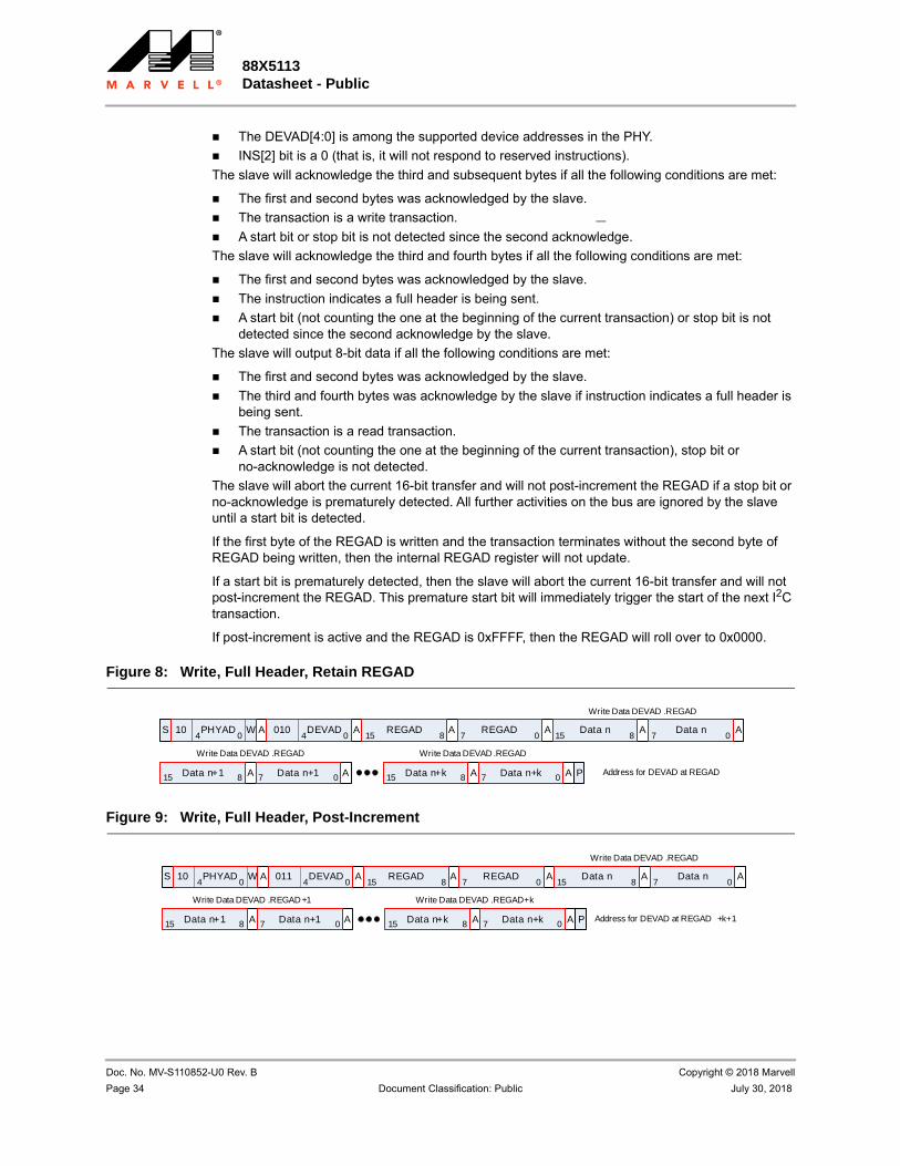
88X5113 Datasheet - Public
Doc. No. MV-S110852-U0 Rev. B Copyright © 2018 Marvell
Page 34 Document Classification: Public July 30, 2018
The DEVAD[4:0] is among the supported device addresses in the PHY.
INS[2] bit is a 0 (that is, it will not respond to reserved instructions).
The slave will acknowledge the third and subsequent bytes if all the following conditions are met:
The first and second bytes was acknowledged by the slave.
The transaction is a write transaction.
A start bit or stop bit is not detected since the second acknowledge.
The slave will acknowledge the third and fourth bytes if all the following conditions are met:
The first and second bytes was acknowledged by the slave.
The instruction indicates a full header is being sent.
A start bit (not counting the one at the beginning of the current transaction) or stop bit is not detected since the second acknowledge by the slave.
The slave will output 8-bit data if all the following conditions are met:
The first and second bytes was acknowledged by the slave.
The third and fourth bytes was acknowledge by the slave if instruction indicates a full header is being sent.
The transaction is a read transaction.
A start bit (not counting the one at the beginning of the current transaction), stop bit or no-acknowledge is not detected.
The slave will abort the current 16-bit transfer and will not post-increment the REGAD if a stop bit or no-acknowledge is prematurely detected. All further activities on the bus are ignored by the slave until a start bit is detected.
If the first byte of the REGAD is written and the transaction terminates without the second byte of REGAD being written, then the internal REGAD register will not update.
If a start bit is prematurely detected, then the slave will abort the current 16-bit transfer and will not post-increment the REGAD. This premature start bit will immediately trigger the start of the next I2C transaction.
If post-increment is active and the REGAD is 0xFFFF, then the REGAD will roll over to 0x0000.
Figure 8: Write, Full Header, Retain REGAD
Figure 9: Write, Full Header, Post-Increment
S 10 PHYAD4 0
W A 010 DEVAD4 0
REGAD15 8
AA REGAD7 0
A Data n15 8
A Data n7 0
A
Write Data DEVAD .REGAD
Data n+115 8 A Data n+17 0 A
Write Data DEVAD .REGAD
Data n+k15 8 A Data n+k7 0 A
Write Data DEVAD .REGAD
P Address for DEVAD at REGAD
S 10 PHYAD4 0
W A 011 DEVAD4 0
REGAD15 8
AA REGAD7 0
A Data n15 8
A Data n7 0
A
Write Data DEVAD .REGAD
Data n+115 8 A Data n+17 0 A
Write Data DEVAD .REGAD+1
Data n+k15 8 A Data n+k7 0 A
Write Data DEVAD .REGAD+k
P Address for DEVAD at REGAD +k+1
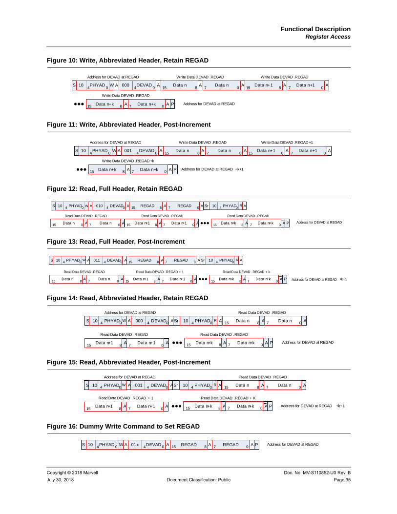
Functional DescriptionRegister Access
Copyright © 2018 Marvell Doc. No. MV-S110852-U0 Rev. B
July 30, 2018 Document Classification: Public Page 35
Figure 10: Write, Abbreviated Header, Retain REGAD
Figure 11: Write, Abbreviated Header, Post-Increment
Figure 12: Read, Full Header, Retain REGAD
Figure 13: Read, Full Header, Post-Increment
Figure 14: Read, Abbreviated Header, Retain REGAD
Figure 15: Read, Abbreviated Header, Post-Increment
Figure 16: Dummy Write Command to Set REGAD
S 10 PHYAD4 0
W A 000 DEVAD4 0
A Data n15 8
A Data n7 0
A
Write Data DEVAD .REGAD
Data n+115 8
A Data n+17 0
A
Write Data DEVAD .REGAD
Data n+k15 8 A Data n+k7 0 A
Write Data DEVAD .REGAD
P
Address for DEVAD at REGAD
Address for DEVAD at REGAD
S 10 PHYAD4 0
W A 001 DEVAD4 0
A Data n15 8
A Data n7 0
A
Write Data DEVAD .REGAD
Data n+115 8
A Data n+17 0
A
Write Data DEVAD .REGAD+1
Data n+k15 8 A Data n+k7 0 A
Write Data DEVAD .REGAD+k
P
Address for DEVAD at REGAD
Address for DEVAD at REGAD +k+1
A
S 10 PHYAD4 0 W A 010 DEVAD4 0 REGAD15 8 AA REGAD7 0 A
Read Data DEVAD .REGAD Read Data DEVAD .REGAD Read Data DEVAD .REGAD
P Address for DEVAD at REGADAAData n15 8 Data n7 0 AAData n+115 8 Data n+17 0 AData n+k15 8 Data n+k7 0
Sr 10 PHYAD4 0R A
A
S 10 PHYAD4 0W A 011 DEVAD4 0 REGAD15 8 AA REGAD7 0 A
Read Data DEVAD .REGAD Read Data DEVAD .REGAD + 1 Read Data DEVAD .REGAD + k
P Address for DEVAD at REGAD +k+1AAData n15 8
Data n7 0
AAData n+115 8
Data n+17 0
AData n+k15 8
Data n+k7 0
Sr 10 PHYAD4 0R A
A
S 10 PHYAD4 0W A 000 DEVAD4 0 A
Read Data DEVAD .REGAD
Read Data DEVAD .REGAD Read Data DEVAD .REGAD
P Address for DEVAD at REGAD
AAData n15 8 Data n7 0
AAData n+115 8
Data n+17 0
AData n+k15 8 Data n+k7 0
Address for DEVAD at REGAD
Sr 10 PHYAD4 0R A
A
S 10 PHYAD4 0W A 001 DEVAD4 0 A
Read Data DEVAD .REGAD
Read Data DEVAD .REGAD + 1 Read Data DEVAD .REGAD + K.
P Address for DEVAD at REGAD +k+1
AAData n15 8 Data n7 0
AAData n+115 8
Data n+17 0
AData n+k15 8 Data n+k7 0
Address for DEVAD at REGAD
Sr 10 PHYAD4 0R A
S 10 PHYAD4 0 W A 01x DEVAD4 0 REGAD15 8 AA REGAD7 0 A P Address for DEVAD at REGAD

88X5113 Datasheet - Public
Doc. No. MV-S110852-U0 Rev. B Copyright © 2018 Marvell
Page 36 Document Classification: Public July 30, 2018
3.5 TWSI, GPIO, and LED
3.5.1 GPIO[3:0] and LED[3:0]The GPIO pins are shared between the GPIO and LED functional modes. Each pin can be programmed independently to operate in GPIO or LED modes. The pin mapping is summarized in Table 18.
GPIO[0] pin is configured to GPIO mode by setting register bits 31.F437.15:14 to 01. This pin can be configured in LED mode by setting register bits 31.F437.15:14 to 10.
The GPIO[3:1] are similar and are configured in GPIO mode by setting register bits 31.F439.15 (for GPIO[1]), 31.F43B.15 (GPIO[2]), and 31.F43D.15 (GPIO[3]) to 0 individually. These pins can be configured in LED mode by setting register bits 31.F439.15 (for GPIO[1]), 31.F43B.15 (GPIO[2]), and 31.F43D.15 (GPIO[3]) to 1 individually.
In GPIO mode, each pin can operate bidirectionally and can be individually configured. In the input mode, these pins can be used as interrupts. The GPIO operations are described in the sections below.
3.5.1.1 Controlling and SensingIn the GPIO mode, registers 31.F437.13, 31.F439.13, 31.F43B.13, and 31.F43D.13 control whether the GPIO pins are inputs or outputs. Each pin can be individually controlled. Registers 31.F437.7, 31.F439.7, 31.F43B.7, and 31.F43D.7 allow the pins to be controlled and sensed. When configured as input, a read to registers 31.F437.7, 31.F439.7, 31.F43B.7 and 31.F43D.7 will return the real-time sampled state of the pins GPIO[0], GPIO[1], GPIO[2], and GPIO[3], respectively at the time of the read. A write to these register will write to the output register, but have no immediate effect on the pin since the pin is configured to be an input. The input is sampled once every 6.4 ns (equivalent to one reference clock period). When configured as output, a write will write to the output register which will in turn drive the state of the pin. A read to registers 31.F437.7, 31.F439.7, 31.F43B.7, and 31.F43D.7 will return the value in the output registers.
3.5.1.2 GPIO InterruptsWhen the GPIO pins are configured as input, several types of interrupt events can be generated as described in Table 19. Register bits 31.F437.10:8, 31.F439.10:8, 31.F43B.10:8, and 31.F43D.10:8 allow each pin to be configured to generate interrupt on one of 5 types of events - Low Level, High Level, High to Low Transition, Low to High Transition, and Transitions on Either Edge. The interrupt generation can also be disabled. When an interrupt event is generated on pin GPIO[0], it is latched
Table 18: GPIO, LED Signal Mapping
Pin Special Funct ion GPIO LED
GPIO[0] – GPIO[0] LED[0]
GPIO[1] – GPIO[1] LED[1]
GPIO[2] – GPIO[2] LED[2]
GPIO[3] – GPIO[3] LED[3]

Functional DescriptionTWSI, GPIO, and LED
Copyright © 2018 Marvell Doc. No. MV-S110852-U0 Rev. B
July 30, 2018 Document Classification: Public Page 37
high in the sticky register 31.F437.11. Similarly, when interrupt event is generated on GPIO[1], GPIO[2] or GPIO[3], they are latched in the sticky register 31.F439.11, 31.F43B.11, and 31.F43D.11. The register bits will remain high until read. The GPIO interrupt can be asserted when an event occurs through pins GPIO[3:0]. Registers 31.F437.12, 31.F439.12, 31.F43B.12, and 31.F43D.12 set the interrupt enables.
Registers 31.F437.12 and 31.F437.11 are bitwise AND together to generate a GPIO[0] interrupt. Registers 31.F439.12 and 31.F439.11 are bitwise AND together to generate a GPIO[1] interrupt. Similarly, registers 31.F43B.12 and 31.F43B.11 are bitwise AND together to generate a GPIO[2] interrupt and registers 31.F43D.12 and 31.F43D.11 are bitwise AND together to generate a GPIO[3] interrupt. If the result is non-zero the GPIO interrupt will assert. For interrupt polarity control, refer to Table 19.
Table 19: GPIO/LED Controls
Register Funct ion Setting Mode
31.F437.15:14 GPIO 0 Function 00 = GPIO[0] is used for signaling. 01 = GPIO[0] is used for GPIO 0 function. 10 = GPIO[0] is used for LED 0 function. 11 = Reserved. (LED 0 can only select lane 0 as LED function)
R/W
31.F439.1531.F43B.1531.F43D.15
GPIO n Functionwhere n = 1, 2, 3
0 = GPIO [n] pin is used for GPIO 1 function.1 = GPIO [n] pin is used for LED 1 function.(LED n can only select lane n as LED function)
R/W
31.F437.1331.F439.1331.F43B.1331.F43D.13
LED n Output Enablewhere n = 0, 1, 2, 3
This bit has no effect unless register 31.F437.15:14 = 01. 0 = Input 1 = Output
R/W
31.F437.1231.F439.1231.F43B.1231.F43D.12
GPIO n Interrupt Enablewhere n = 0, 1, 2, 3
0 = Disable 1 = Enable
R/W
31.F437.1131.F439.1131.F43B.1131.F43D.11
GPIO n Interrupt Statuswhere n = 0, 1, 2, 3
This bit is not valid unless register 31.F437.15:14 = 01 and 31.F437.13 = 0. 0 = No interrupt has occurred. 1 = An interrupt has occurred.
RO, LH
31.437.10:831.F439.10:831.F43B.10:831.F43D.10:8
GPIO n Interrupt Selectwhere n = 0, 1, 2, 3
Interrupt is effective only when 31.F437.13 = 0.000 = No Interrupt 001 = Reserved 010 = Interrupt on Low Level 011 = Interrupt on High Level 100 = Interrupt on High to Low 101 = Interrupt on Low to High 110 = Reserved 111 = Interrupt on Low to High or High to Low
R/W

88X5113 Datasheet - Public
Doc. No. MV-S110852-U0 Rev. B Copyright © 2018 Marvell
Page 38 Document Classification: Public July 30, 2018
3.5.1.3 LEDThe GPIO[3:0] pins can be used to drive LED pins. Setting register 31.F437.15:14 to 10 and registers 31.F439.15, 31.F43B.15, and 31.F43D.15 to 1 will configure the GPIO[0], GPIO[1], GPIO[2], GPIO[3] pin in the LED mode and named as LED[0], LED[1], LED[2] and LED[3]. Registers 31.F438, 31.F43A, 31.F43C, and 31.F43E control the operation of the LED pins. LED[3:0] will operate per this section unless the pin is used for GPIO purposes. Figure 17 shows the general chaining of function for the LEDs. The various functions are described in the following sections. All LED pins are tri-state outputs.
Figure 17: LED Chain
LED OperationsThe LED pins relay various statuses of the PHY so that they can be displayed by the LEDs.
The status that the LEDs display is defined by registers 31.F438, 31.F43A, 31.F43C, and 31.F43E as shown in Table 20. For each LED, if the condition selected by bits 11:8 is true, then the LED will blink. If the condition selected by bits 7:4 is true, then the LED will be solid on. If both selected conditions are true, then the blink will take precedence.
LED0 displays the status of lane 0, and LED1 displays the status of lane 1, and so on. Register bit 31.F438.12 is set to 1 to display the status of system (host) side transmit activity, receive activity and link status register on LED 0. Setting 31.F438.12 to 0 will display the status of line side on LED 0. Similarly, register bits 31.F43A.12, 31.F43C.12, and 31.F43E.12 are used to select the status of the host side or the line side for LED1, LED2, and LED3.
31.F437.731.F439.731.F43B.731.F43D.7
GPIO n Datawhere n = 0, 1, 2,3
This bit has no effect unless register 31.F437.15:14 = 01. When 31.F437.13 = 0, a read to this register will reflect the state of the GPIO[0], and a write will write the output register but have no effect on the GPIO[n].When 31.F437.13 = 1 a read to this register will reflect the state of the output register, and a write will write the output register and drive the state of the GPIO[n].
R/W
31.F437.6:031.F439.6:031.F43B.6:031.F43D.6:0
Reserved Set to 0s. RO
Table 19: GPIO/LED Controls (Continued)
Register Funct ion Setting Mode
PulseStretch
ReceiveActivity
PulseStretch
TransmitActivity
Logic
Link Status
ManualOverride
and Control
Blink
Logic
Mix
LogicGPIO/LEDGPIO

Functional DescriptionTWSI, GPIO, and LED
Copyright © 2018 Marvell Doc. No. MV-S110852-U0 Rev. B
July 30, 2018 Document Classification: Public Page 39
LED PolarityThere are a variety of methods to hook up the LEDs. Some examples are shown in Figure 18. Registers 31.F438.1:0, 31.F43A.1:0, 31.F43C.1:0, and 31.F43E.1:0 specify the output polarity for the LED function to accommodate a variety of installation options. The lower bit of each pair specified the on (active) state of the LED, either high or low. The upper bit of each pair specifies whether the off state of the LED should be driven to the opposite level of the on state or Hi-Z.
Figure 18: Various LED Hookup Configurations
Single LED -High Active
Single LED -Low Active
Three terminalbi-color LED -High Active
Three terminalbi-color LED -
Low Active
Two terminalbi-color LED
Table 20: LED[3:0] Control and Status Register Bits
Register Function Sett ing Mode
31.F438.15:1331.F43A.15:1331.F43C.15:1331.F43E.15:13
Reserved Scratch reserved register R/W
31.F438.1231.F43A.1231.F43C.1231.F43E.12
LED[n] PHY/System side selectWhere n = 0, 1, 2, 3
0 = PHY side (line side). 1 = System side (host side).
R/W
31.F438.11:831.F43A.11:831.F43C.11:831.F43E.11:8
LED[n] Blink BehaviorWhere n = 0, 1, 2, 3
Blink Behavior has higher priority. 0000 = Solid Off 0001 = System or Line Side Transmit or Receive Activity 0010 = System or Line Side Transmit Activity 0011 = System or Line Side Receive Activity 0100 = Reserved 0101 = Reserved 0110 = System or Line Side Side Link 0111 = Solid On1000 = Reserved 1001 = Reserved 1010 = Blink Mix 1011 = Solid Mix 11xx = Reserved
R/W

88X5113 Datasheet - Public
Doc. No. MV-S110852-U0 Rev. B Copyright © 2018 Marvell
Page 40 Document Classification: Public July 30, 2018
Pulse Stretching and BlinkingRegister 31.F435.14:12 specifies the pulse stretching duration for a particular activity. Only the transmit activity, receive activity, and (transmit or receive) activity are stretched. All other statuses are not stretched since they are static in nature and no stretching is required.
Some status will require blinking instead of a solid on. Registers 31.F435.10:8 and 31.F435.6:4 specify the two blink rates. The pulse stretching is applied first and the blinking will reflect the duration of the stretched pulse. Registers 31.F438.2, 31.F43A.2, 31.F43C.2, and 31.F43E.2 select which of the two blink rates to use for LED0 to LED3, respectively.
0 = Select Blink Rate 1.
1 = Select Blink Rate 2.
31.F438.7:431.F43A.7:431.F43C.7:431.F43E.7:4
LED[n] Solid BehaviorWhere n = 0, 1, 2, 3
Blink Behavior has higher priority.0000 = Solid Off 0001 = System or Line Side Transmit or Receive Activity 0010 = System or Line Side Transmit Activity 0011 = System or Line Side Receive Activity 0100 = Reserved 0101 = Reserved 0110 = System or Line Side Link 0111 = Solid On 1xxx = Reserved
R/W
31.F438.331.F43A.331.F43C.331.F43E.3
Reserved Set to 0. R/W
31.F438.231.F43A.231.F43C.231.F43E.2
LED[n] Blink Rate SelectWhere n = 0, 1, 2, 3
0 = Select Blink Rate 1 1 = Select Blink Rate 2
R/W
31.F438.1:031.F43A.1:031.F43C.1:031.F43E.1:0
LED[n] PolarityWhere n = 0, 1, 2, 3
00 = On - drive LED[n] low, Off - drive LED[n] high 01 = On - drive LED[n] high, Off - drive LED[n] low 10 = On - drive LED[n] low, Off - tri-state LED[n] 11 = On - drive LED[n] high, Off - tri-state LED[n]
Table 20: LED[3:0] Control and Status Register Bits (Continued)
Register Function Sett ing Mode
Table 21: LED Timer Control
Register Funct ion Sett ing Mode
31.F435.15 Reserved Set to 0. R/W

Functional DescriptionTWSI, GPIO, and LED
Copyright © 2018 Marvell Doc. No. MV-S110852-U0 Rev. B
July 30, 2018 Document Classification: Public Page 41
31.F435.14:12 Pulse Stretch Duration 000 = No pulse stretching 001 = 20 to 40 ms 010 = 40 to 81 ms 011 = 81 to 161 ms 100 = 161 to 322 ms 101 = 322 to 644 ms 110 = 644 ms to 1.3s 111 = 1.3 to 2.6s
R/W
31.F435.11 Reserved Set to 0. R/W
31.F435.10:8 Blink Rate 2 000 = 40 ms 001 = 81 ms 010 = 161 ms 011 = 322 ms 100 = 644 ms 101 = 1.3s 110 = 2.6s 110 = 5.2s
R/W
31.F435.7 Reserved Set to 0. R/W
31.F435.6:4 Blink Rate 1 000 = 40 ms 001 = 81 ms 010 = 161 ms 011 = 322 ms 100 = 644 ms 101 = 1.3s 110 = 2.6s 110 = 5.2s
R/W
31.F435.3:0 Reserved Set to 0. R/W
Table 21: LED Timer Control (Continued)
Register Funct ion Sett ing Mode

88X5113 Datasheet - Public
Doc. No. MV-S110852-U0 Rev. B Copyright © 2018 Marvell
Page 42 Document Classification: Public July 30, 2018
3.5.2 TWSI, GPIO 4, and GPIO 5The SCL and SDA pins are for TWSI mode and have the option to be used for GPIO functional mode. In TWSI mode, the SCL and SDA pins are coupled together, where the SCL pin is used as a clock, and SDA is used as a serial bidirectional data. The pin mapping is summarized in Table 22.
The SCL and SDA pins are configured to TWSI mode by setting 31.F430.14 to 0. TWSI is the default mode for these pins. SCL pin is configured in GPIO mode by setting register bits 31.F430.14 to 1. Similarly, SDA pin is configured in GPIO mode by setting register bits 31.F432.14 to 1.
TWSI is the two-wire serial interface standard. In a special mode, TWSI is used to load the SERDES and chip management firmware from an external EEPROM immediately after the reset is de-asserted. EEPROM is attached to the TWSI interface via the SCL and SDA pins. This interface can also be used to write the external EEPROM from an internal RAM using the embedded processor.
Table 22: TWSI and GPIO Signal Mapping
Pin GPIO TWSI
SCL GPIO[4] TWSI clock (SCL)
SDA GPIO[5] TWSI serial data (SDA)
Table 23: SCL Control
Register Function Sett ing Mode
31.F430.15 Reserved Reserved RO
31.F430.14 SCL Function TWSI mode for SCL and SDA pins are selected by 31.F430.14 only. Register 31.F432.14 has no effect on TWSI mode. GPIO functions are controlled individually for each pin. 0 = SCL/SDA is used for TWSI Function. 1 = SCL is used for GPIO Function, if 31.F427.7 = 0. 1 = SCL is used for divided recovered clock B, when 31.F427.7 = 1.
R/W
31.F430.13 SCL Output Enable
This bit has no effect unless register 31.F430.14 = 1 and 31.F427.7 = 0. 0 = Input 1 = Output
R/W
31.F430.12 SCL Interrupt Enable
0 = Disable 1 = Enable
R/W
31.F430.11 SCL Interrupt Status
This bit is not valid unless register 31.F430.14 = 1 and 31.F430.13 = 0. 0 = No interrupt has occurred. 1 = An interrupt has occurred.
RO, LH

Functional DescriptionTWSI, GPIO, and LED
Copyright © 2018 Marvell Doc. No. MV-S110852-U0 Rev. B
July 30, 2018 Document Classification: Public Page 43
31.F430.10:8 SCL Interrupt Select
Interrupt is effective only when 31.F430.13 = 0.000 = No Interrupt 001 = Reserved 010 = Interrupt on Low Level 011 = Interrupt on High Level 100 = Interrupt on High to Low 101 = Interrupt on Low to High 110 = Reserved 111 = Interrupt on Low to High or High to Low
R/W
31.F430.7 SCL GPIO Data
This bit has no effect unless register 31.F430.14 = 1. When 31.F430.13 = 0, a read to this register will reflect the state of the SCL pin, and a write will write the output register but have no effect on the SCL pin.
When 31.F430.13 = 1, a read to this register will reflect the state of the output register, and a write will write the output register and drive the state of the SCL pin.
R/W
31.F430.6:0 Reserved Set to 0s. RO
Table 23: SCL Control (Continued)
Register Function Sett ing Mode
Table 24: SDA Control
Register Funct ion Sett ing Mode
31.F432.15 Reserved Reserved. RO
31.F432.14 SDA Function TWSI mode for SCL and SDA pins are selected by 31.F430.14 only. Register 31.F432.14 has no effect on TWSI mode, but can enable the GPIO or Recovered clock output function on this pin. 0 = Reserved 1 = SDA is used for GPIO 5 Function if 31.F427.11 = 0. 1 = SDA is used for divided recovered clock C if 31.F427.11 = 1.
R/W
31.F432.13 SDA Output Enable This bit has no effect unless register 31.F432.14 = 1 and register 31.LT27.11 = 0. 0 = Input 1 = Output
R/W
31.F432.12 SDA Interrupt Enable 0 = Disable 1 = Enable
R/W
31.F432.11 SDA Interrupt Status This bit is not valid unless register 31.F432.14 = 1 and register 31.F432.13 = 0. 0 = No interrupt has occurred. 1 = An interrupt has occurred.
RO, LH

88X5113 Datasheet - Public
Doc. No. MV-S110852-U0 Rev. B Copyright © 2018 Marvell
Page 44 Document Classification: Public July 30, 2018
31.F432.10:8 SDA Interrupt Select Interrupt is effective only when 31.F432.13 = 0.000 = No Interrupt 001 = Reserved 010 = Interrupt on Low Level 011 = Interrupt on High Level 100 = Interrupt on High to Low 101 = Interrupt on Low to High 110 = Reserved 111 = Interrupt on Low to High or High to Low
R/W
31.F432.7 SDA GPIO Data This bit has no effect unless register 31.F432.14 = 1. When 31.F432.13 = 0, a read to this register will reflect the state of the SDA pin, and a write will write the output register but have no effect on the SDA pin.When 31.F432.13 = 1, a read to this register will reflect the state of the output register, and a write will write the output register and drive the state of the SDA pin.
R/W
31.F432.6:0 Reserved Set to 0s. RO
Table 24: SDA Control (Continued)
Register Funct ion Sett ing Mode

Functional DescriptionTWSI, GPIO, and LED
Copyright © 2018 Marvell Doc. No. MV-S110852-U0 Rev. B
July 30, 2018 Document Classification: Public Page 45
Table 25: I/O Open Drain Control
Register Funct ion Setting Mode
Port031.F436.15:3
Reserved Set to 0. R/W
Port031.F436.2
GPIO1 pin (port0 GPIO[0]) open drain control
0 = Pad can drive high.1 = Pad cannot drive high (Set to high when open drain pad is used).
R/W
Port031.F436.1:0
Reserved Set to 0. R/W
Port131.F436.15:7
Reserved Set to 0. R/W
Port131.F436.6
GPIO2 pin (port1 GPIO[4]) open drain control
0 = Pad can drive high.1 = Pad cannot drive high (Set to high when open drain pad is used).
R/W
Port131.F436.5:4
Reserved Set to 0. R/W
Port231.F436.15:3
Reserved Set to 0. R/W
Port231.F436.2
GPIO3 pin (port2 GPIO[0]) open drain control
0 = Pad can drive high.1 = Pad cannot drive high (Set to high when open drain pad is used).
R/W
Port231.F436.1:0
Reserved Set to 0. R/W
Port331.F436.7
CLK_OUT_SE2 pin (port3 GPIO[5]) open drain control
0 = Pad can drive high.1 = Pad cannot drive high (Set to high when open drain pad is used).
R/W
Port331.F436.6
CLK_OUT_SE1 pin (port3 GPIO[4]) open drain control
0 = Pad can drive high.1 = Pad cannot drive high (Set to high when open drain pad is used).
R/W
Port331.F436.5
Reserved Set to 0. R/W
Port331.F436.4
GPIO4 pin (port3 GPIO[2]) open drain control
0 = Pad can drive high.1 = Pad cannot drive high (Set to high when open drain pad is used).
R/W
Port331.F436.3:0
Reserved Set to 0. R/W

88X5113 Datasheet - Public
Doc. No. MV-S110852-U0 Rev. B Copyright © 2018 Marvell
Page 46 Document Classification: Public July 30, 2018
3.5.3 Two-wire Serial Interface (TWSI)TWSI is used to load the SERDES and chip management firmware from an external EEPROM. EEPROM is attached to the TWSI interface via the SCL and SDA pins. This interface can also be used to write the external EEPROM from an internal RAM using the embedded processor. External pull up resisters are required to connect to SCL and SDA pins.
3.6 InterruptVarious functional units in the device can generate interrupt on the INTn pin. The INTn interrupt pin will be active if any of the events enabled in the interrupt enable register occurs. If an interrupt event corresponding to a disabled interrupt enable bit occurs, then the corresponding interrupt status bit will be set even though the event does not activate the INTn pin.
By default, the INTn is driven low when an enabled interrupt is active. The polarity of the INTn pin can be changed by programming register 31.F421.2:1. The INTn pin can also be forced to be active by setting the register 31.F421.0 to 1.
The interrupts are cleared after a read to the interrupt status register. F
The Global Interrupt Status register (Table 27) summarizes which unit is requesting the interrupt. The interrupts are logically ORed along with register 31.F421.0 to form the interrupt output (INTn). The Global Interrupt Status register bits do not have corresponding Interrupt Enable bits. All the interrupt enables/masks are located within each unit.
Table 26: Global Interrupt Control
Register Funct ion Sett ing
31.F421.2:1 Interrupt Polarity 00 = Active - drive INT low, Inactive - drive INT high 01 = Active - drive INT high, Inactive - drive INT low 10 = Active - drive INT low, Inactive - tri-state INT 11 = Active - drive INT high, Inactive - tri-state INT
31.F421.0 Force Interrupt Pin Active
0 = Normal operation 1 = Force interrupt pin active.

Functional DescriptionInterrupt
Copyright © 2018 Marvell Doc. No. MV-S110852-U0 Rev. B
July 30, 2018 Document Classification: Public Page 47
Figure 19 diagram shows the interrupt hierarchy and aggregation from different blocks.
Figure 19: Interrupt Hierarchy and Aggregation from Different Blocks
Table 28, Table 29, Table 30, and Table 31 summarize the Line Side (N Unit) interrupt control and statuses for various interface modes. Excessive link error can be monitored to generate an interrupt event (See Table 32).
The Host Side (M Unit) has the same set of interrupt function with the exception that the device register is 4 (instead of 3).
ExcessLink ErrorInterrupt
1G/2.5GPCS
Interrupt
5G/10G/25GPCS
Interrupt
40G/50GPCS
Interrupt
100GPCS
Interrupt
200GPCS
Interrupt
Line SideLevel 2
InterruptAggregation
(OR)
Host SideLevel 2
InterruptAggregation
(OR)
...
ProcessorInterrupt
40G to 25GRate
MatchingFIFO
Interrupt
GPIOInterrupt
Port LevelLevel 1
InterruptAggregation
(OR)
Interruptper port
Table 27: Global Interrupt Status
Bit Descript ions Register
Temp Sensor Interrupt Status 31.F420.11
GPIO Interrupt Status 31.F420.10
RM_FIFO Interrupt Status 31.F420.9
On-chip Processor Interrupt Status 31.F420.8
M0 Interrupt Status 31.F420.4
N0 Interrupt Status 31.F420.0

88X5113 Datasheet - Public
Doc. No. MV-S110852-U0 Rev. B Copyright © 2018 Marvell
Page 48 Document Classification: Public July 30, 2018
Each bit of the Interrupt Status register will be masked with the Interrupt Enable register, respectively, and each enabled output is ORed to form the aggregated unit interrupt. The Port Interrupt Statuses (register 31.F004.0 – Line Side Interrupt, register 31.F004.2 – System Side Interrupt) are the result of logical OR of the aggregated unit interrupt.
Where n = 0, 2, 4, 6 for Lane 0, 1, 2, and 3, respectively.
Where n = 0, 2, 4, 6 for Lane 0, 1, 2, and 3, respectively.
Table 28: 1G/2.5G Interrupt Enable, Interrupt Status, and Real-Time Status
Bit Descriptions Interrupt Enable
Interrupt Status
Real-Time Status
Speed Changed 3.Bn01.14 3.Bn02.14 –
Duplex Changed 3.Bn01.13 3.Bn02.13 –
Page Received 3.Bn01.12 3.Bn02.12 –
Auto-Negotiation Completed 3.Bn01.11 3.Bn02.11 –
Link Up to Link Down 3.Bn01.10 3.Bn02.10 –
Link Down to Link Up 3.Bn01.9 3.Bn02.9 –
Symbol Error 3.Bn01.8 3.Bn02.8 –
False Carrier 3.Bn01.7 3.Bn02.7 –
Table 29: 10G/25G Interrupt Enable, Interrupt Status, and Real-Time Status
Bit Descriptions Interrupt Enable
Interrupt Status
Real-Time Status
Local Fault Transmitted 3.An00.11 3.An01.11 3.An02.11
Local Fault Received 3.An00.10 3.An01.10 3.An02.10
Rx FIFO Full 3.An00.6 3.An01.6 3.An02.6
Rx FIFO Empty 3.An00.5 3.An01.5 3.An02.5
Link Status Change 3.An00.2 3.An01.2 3.An02.2
High BER Change 3.An00.1 3.An01.1 3.An02.1
Block Lock Change 3.An00.0 3.An01.0 3.An02.0
CRC 3.An4A.2 3.An4B.2 –
FIFO Overflow 3.An4A.1 3.An4B.1 –
FIFO Underflow 3.An4A.0 3.An4B.0 –

Functional DescriptionInterrupt
Copyright © 2018 Marvell Doc. No. MV-S110852-U0 Rev. B
July 30, 2018 Document Classification: Public Page 49
Where n = 0, 2, 4, 6 for Lane 0, 1, 2, and 3, respectively.
Table 30: 40G/50G Interrupt Enable, Interrupt Status, and Real-Time Status
Bit Descriptions Interrupt Enable Interrupt Status Real-Time Status
Local Fault Transmitted 3.9001.11 3.9002.11 3.9003.11
Local Fault Received 3.9001.10 3.9002.10 3.9003.10
Lane Alignment 3.9001.9 3.9002.9 3.9003.9
Tx Lane Count err 3.9001.8 3.9002.8 3.9003.8
JIT 0 Lock Change 3.9001.7 3.9002.7 3.9003.7
JIT Local-Fault Lock Change 3.9001.6 3.9002.6 3.9003.6
Link Status Change 3.9001.5 3.9002.5 3.9003.5
High BER Change 3.9001.4 3.9002.4 3.9003.4
Lane 3:0 Block Lock Change 3.9001.3:0 3.9002.3:0 3.9003.3:0
CRC 3.904A.2 3.904B.2 –
FIFO Overflow 3.904A.1 3.904B.1 –
FIFO Underflow 3.904A.0 3.904B.0 –
Table 31: 100G Interrupt Enable, Interrupt Status, and Real-Time Status
Bit Descriptions Interrupt Enable
Interrupt Status
Real-Time Status
100G PCS Rx FIFO Empty 3.8001.15 3.8003.15 3.8005.15
100G PCS Rx FIFO Full 3.8001.14 3.8003.14 3.8005.14
100G PCS Tx PPM FIFO Overflow 3.8001.13 3.8003.13 3.8005.13
100G PCS Tx PPM FIFO Underflow 3.8001.12 3.8003.12 3.8005.12
Rising Edge of the Local Fault Condition on Tx Path 3.8001.11 3.8003.11 3.8005.11
Rising Edge of the Local Fault Condition on Rx Path 3.8001.10 3.8003.10 3.8005.10
100G Packet Check CRC Error 3.8001.7 3.8003.7 3.8005.7
Link Change 3.8001.5 3.8003.5 3.8005.5
High BER Change 3.8001.4 3.8003.4 3.8005.4
Lane 3:0 Block Lock Change 3.8001.3:0 3.8003.3:0 3.8005.3:0
Lane 19:4 Block Lock Change 3.8002.15:0 3.8004.15:0 3.8006.15:0

88X5113 Datasheet - Public
Doc. No. MV-S110852-U0 Rev. B Copyright © 2018 Marvell
Page 50 Document Classification: Public July 30, 2018
Where n = 0, 2 for Lane 0, 2, respectively.
The interrupt from the processor block is for debug or patch program: details are not provided here (For further details, refer to Section 3.10).
All of the GPIO interrupts are only valid when the multi-function pins are configured as GPIO Inputs.
Table 32: Excessive Link Error Interrupt Enable, Interrupt Status, and Real-Time Status
Bit Descriptions Interrupt Enable
Interrupt Status
Real-Time Status
Excessive Link Error – Lane 0 In 40G/50G/100G mode, only Lane 0 interrupt is used (Lane 1, 2, and 3 interrupts bits are ignored).Register 3.F041.6:0 sets the link error threshold setting. Register 3.F041.7 sets the link down or link up error setting.
3.F041.8 3.F040.15 3.F040.14
Excessive Link Error – Lane 1 Register 3.F043.6:0 sets the link error threshold setting.Register 3.F043.7 sets the link down or link up error setting.
3.F043.8 3.F042.15 3.F042.14
Excessive Link Error – Lane 2 Register 3.F045.6:0 sets the link error threshold setting.Register 3.F045.7 sets the link down or link up error setting.
3.F045.8 3.F044.15 3.F044.14
Excessive Link Error – Lane 3 Register 3.F047.6:0 sets the link error threshold setting.Register 3.F047.7 sets the link down or link up error setting.
3.F047.8 3.F046.15 3.F046.14
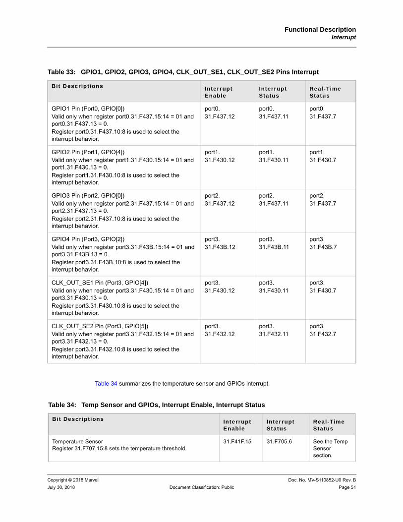
Functional DescriptionInterrupt
Copyright © 2018 Marvell Doc. No. MV-S110852-U0 Rev. B
July 30, 2018 Document Classification: Public Page 51
Table 34 summarizes the temperature sensor and GPIOs interrupt.
Table 33: GPIO1, GPIO2, GPIO3, GPIO4, CLK_OUT_SE1, CLK_OUT_SE2 Pins Interrupt
Bit Descriptions Interrupt Enable
Interrupt Status
Real-Time Status
GPIO1 Pin (Port0, GPIO[0]) Valid only when register port0.31.F437.15:14 = 01 and port0.31.F437.13 = 0.Register port0.31.F437.10:8 is used to select the interrupt behavior.
port0.31.F437.12
port0.31.F437.11
port0.31.F437.7
GPIO2 Pin (Port1, GPIO[4]) Valid only when register port1.31.F430.15:14 = 01 and port1.31.F430.13 = 0.Register port1.31.F430.10:8 is used to select the interrupt behavior.
port1.31.F430.12
port1.31.F430.11
port1.31.F430.7
GPIO3 Pin (Port2, GPIO[0]) Valid only when register port2.31.F437.15:14 = 01 and port2.31.F437.13 = 0.Register port2.31.F437.10:8 is used to select the interrupt behavior.
port2.31.F437.12
port2.31.F437.11
port2.31.F437.7
GPIO4 Pin (Port3, GPIO[2]) Valid only when register port3.31.F43B.15:14 = 01 and port3.31.F43B.13 = 0.Register port3.31.F43B.10:8 is used to select the interrupt behavior.
port3.31.F43B.12
port3.31.F43B.11
port3.31.F43B.7
CLK_OUT_SE1 Pin (Port3, GPIO[4]) Valid only when register port3.31.F430.15:14 = 01 and port3.31.F430.13 = 0.Register port3.31.F430.10:8 is used to select the interrupt behavior.
port3.31.F430.12
port3.31.F430.11
port3.31.F430.7
CLK_OUT_SE2 Pin (Port3, GPIO[5]) Valid only when register port3.31.F432.15:14 = 01 and port3.31.F432.13 = 0.Register port3.31.F432.10:8 is used to select the interrupt behavior.
port3.31.F432.12
port3.31.F432.11
port3.31.F432.7
Table 34: Temp Sensor and GPIOs, Interrupt Enable, Interrupt Status
Bit Descript ions Interrupt Enable
Interrupt Status
Real-Time Status
Temperature SensorRegister 31.F707.15:8 sets the temperature threshold.
31.F41F.15 31.F705.6 See the Temp Sensor section.

88X5113 Datasheet - Public
Doc. No. MV-S110852-U0 Rev. B Copyright © 2018 Marvell
Page 52 Document Classification: Public July 30, 2018
GPIO 0 (LED 0)Valid only when register 31.F437.15:14 = 01 and 31.F437.13 = 0.Register 31.F437.10:8 is used to select the interrupt behavior.
31.F437.12 31.F437.11 31.F437.7
GPIO 1 (LED 1)Valid only when register 31.F439.15=0 and 31.F439.13 = 0.Register 31.F439.10:8 is used to select the interrupt behavior.
31.F439.12 31.F439.11 31.F439.7
GPIO 2 (LED 2)Valid only when register 31.F43B.15=0 and 31.F43B.13 = 0.Register 31.F43B.10:8 is used to select the interrupt behavior.
31.F43B.12 31.F43B.11 31.F43B.7
GPIO 3 (LED 3)Valid only when register 31.F43D.15=0 and 31.F43D.13 = 0.Register 31.F43D.10:8 is used to select the interrupt behavior.
31.F43D.12 31.F43D.11 31.F43D.7
GPIO 4 (SCL)Valid only when register 31.F430.14 = 1, 31.F427.7 = 0, and 31.F430.13 = 0.Register 31.F430.10:8 is used to select the interrupt behavior.
31.F430.12 31.F430.11 31.F430.7
GPIO 5 (SDA)Valid only when register 31.F432.14 = 1, 31.F427.11 = 0, and 31.F432.7 = 0.Register 31.F432.10:8 is used to select the interrupt behavior.
31.F432.12 31.F432.11 31.F432.7
Table 34: Temp Sensor and GPIOs, Interrupt Enable, Interrupt Status (Continued)
Bit Descript ions Interrupt Enable
Interrupt Status
Real-Time Status
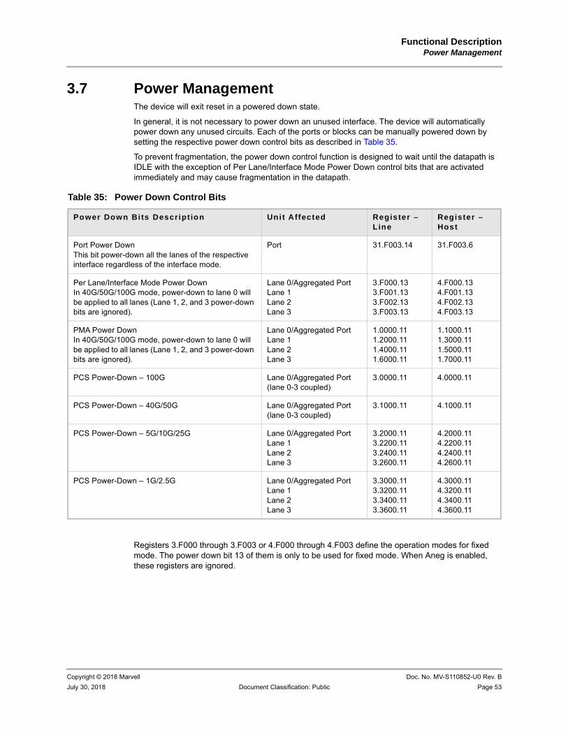
Functional DescriptionPower Management
Copyright © 2018 Marvell Doc. No. MV-S110852-U0 Rev. B
July 30, 2018 Document Classification: Public Page 53
3.7 Power ManagementThe device will exit reset in a powered down state.
In general, it is not necessary to power down an unused interface. The device will automatically power down any unused circuits. Each of the ports or blocks can be manually powered down by setting the respective power down control bits as described in Table 35.
To prevent fragmentation, the power down control function is designed to wait until the datapath is IDLE with the exception of Per Lane/Interface Mode Power Down control bits that are activated immediately and may cause fragmentation in the datapath.
Registers 3.F000 through 3.F003 or 4.F000 through 4.F003 define the operation modes for fixed mode. The power down bit 13 of them is only to be used for fixed mode. When Aneg is enabled, these registers are ignored.
Table 35: Power Down Control Bits
Power Down Bits Descript ion Unit Affected Register – L ine
Register – Host
Port Power DownThis bit power-down all the lanes of the respective interface regardless of the interface mode.
Port 31.F003.14 31.F003.6
Per Lane/Interface Mode Power DownIn 40G/50G/100G mode, power-down to lane 0 will be applied to all lanes (Lane 1, 2, and 3 power-down bits are ignored).
Lane 0/Aggregated PortLane 1Lane 2Lane 3
3.F000.133.F001.133.F002.133.F003.13
4.F000.134.F001.134.F002.134.F003.13
PMA Power DownIn 40G/50G/100G mode, power-down to lane 0 will be applied to all lanes (Lane 1, 2, and 3 power-down bits are ignored).
Lane 0/Aggregated Port Lane 1Lane 2Lane 3
1.0000.111.2000.111.4000.111.6000.11
1.1000.111.3000.111.5000.111.7000.11
PCS Power-Down – 100G Lane 0/Aggregated Port (lane 0-3 coupled)
3.0000.11 4.0000.11
PCS Power-Down – 40G/50G Lane 0/Aggregated Port (lane 0-3 coupled)
3.1000.11 4.1000.11
PCS Power-Down – 5G/10G/25G Lane 0/Aggregated PortLane 1Lane 2Lane 3
3.2000.113.2200.113.2400.113.2600.11
4.2000.114.2200.114.2400.114.2600.11
PCS Power-Down – 1G/2.5G Lane 0/Aggregated PortLane 1Lane 2Lane 3
3.3000.113.3200.113.3400.113.3600.11
4.3000.114.3200.114.3400.114.3600.11

88X5113 Datasheet - Public
Doc. No. MV-S110852-U0 Rev. B Copyright © 2018 Marvell
Page 54 Document Classification: Public July 30, 2018
3.8 IEEE 1149.1 and 1149.6 ControllerThe IEEE 1149.1 standard defines a test access port and boundary-scan architecture for digital inte-grated circuits and for the digital portions of mixed analog/digital integrated circuits. The IEEE 1149.6 standard defines a test access port and boundary-scan architecture for AC-coupled signals.
This standard provides a solution for testing assembled printed circuit boards and other products based on highly complex digital integrated circuits and high-density surface-mounting assembly techniques.
The device implements the instructions shown in Table 36. Upon reset, ID_CODE instruction is selected. The instruction opcodes are shown in Table 36.
The device reserves five pins called the Test Access Port (TAP) to provide test access:
Test Mode Select Input (TMS)
Test Clock Input (TCK)
Test Data Input (TDI)
Test Data Output (TDO)
Test Reset Input (TRSTn)
To ensure race-free operation all input and output data is synchronous with the test clock (TCK). TAP input signals (TMS and TDI) are clocked into the test logic on the rising edge of TCK, while output signal (TDO) is clocked on the falling edge. For additional details refer to the IEEE 1149.1 Boundary Scan Architecture document.
3.8.1 BYPASS InstructionThe BYPASS instruction uses the bypass register. This register contains a single shift-register stage and is used to provide a minimum length serial path between the TDI and TDO pins of the 88X5113 device when test operation is not required. This arrangement allows rapid movement of test data to and from other testable devices in the system.
Table 36: TAP Controller Opcodes
Instruct ion OpCode
EXTEST 00_0x0
SAMPLE/PRELOAD 00_0000_0001
CLAMP 00_0000_0010
HIGH-Z 00_0000_0011
ID_CODE 00_0000_0100
EXTEST_PULSE 00_0000_0101
EXTEST_TRAIN 00_0000_0110
BYPASS 11_1111_1111

Functional DescriptionIEEE 1149.1 and 1149.6 Controller
Copyright © 2018 Marvell Doc. No. MV-S110852-U0 Rev. B
July 30, 2018 Document Classification: Public Page 55
3.8.2 SAMPLE/PRELOAD InstructionThe SAMPLE/PRELOAD instruction enables scanning of the boundary-scan register without causing interference to the normal operation of the device. Two functions are performed when this instruction is selected: sample and preload.
Sample allows a snapshot to be taken of the data flowing from the system pins to the on-chip test logic or vice versa, without interfering with normal operation. The snapshot is taken on the rising edge of TCK in the Capture-DR controller state, and the data can be viewed by shifting through the component's TDO output.
While sampling and shifting data out through TDO for observation, preload enables an initial data pattern to be shifted in through TDI and to be placed at the latched parallel output of the boundary-scan register cells that are connected to system output pins. This step ensures that known data is driven through the system output pins upon entering the extest instruction. Without preload, indeterminate data would be driven until the first scan sequence is complete. The shifting of data for the sample and preload phases can occur simultaneously. While data capture is being shifted out, the preload data can be shifted in.
The boundary scan register for CONFIG[2] is closest to TDO.
Table 37 lists the boundary scan order where:
TDI LIN[0] … CONFIG[2] TDO
Table 37: Boundary Scan Chain Order
Order Bal l Type
1 CONFIG[2] Input
2 CONFIG[1] Input
3 CONFIG[0] Input
4 PHYAD[2] Input
5 PHYAD[3] Input
6 PHYAD[1] Input
7 PHYAD[0] Input
8 INTN Output
9 INTN Output Enable
10 MDC Input
11 MDIO Input
12 MDIO Output
13 MDIO Output Enable
14 HOP[3] AC Output
15 HON[3] AC Output
16 HIP[3] AC Input
17 HIN[3] AC Input

88X5113 Datasheet - Public
Doc. No. MV-S110852-U0 Rev. B Copyright © 2018 Marvell
Page 56 Document Classification: Public July 30, 2018
18 HOP[2] AC Output
19 HON[2] AC Output
20 HIP[2] AC Input
21 HIN[2] AC Input
22 HOP[1] AC Output
23 HON[1] AC Output
24 HIP[1] AC Input
25 HIN[1] AC Input
26 HOP[0] AC Output
27 HON[0] AC Output
28 HIP[0] AC Input
29 HIN[0] AC Input
30 SCL Output Enable
31 SCL Output
32 SCL Input
33 SDA Output Enable
34 SDA Output
35 SDA Input
36 RESETN Input
37 GPIO[0] Output Enable
38 GPIO[0] Output
39 GPIO[0] Input
40 GPIO[1] Output Enable
41 GPIO[1] Output
42 GPIO[1] Input
43 GPIO[2] Output Enable
44 GPIO[2] Output
45 GPIO[2] Input
46 GPIO[3] Output Enable
Table 37: Boundary Scan Chain Order (Continued)
Order Bal l Type

Functional DescriptionIEEE 1149.1 and 1149.6 Controller
Copyright © 2018 Marvell Doc. No. MV-S110852-U0 Rev. B
July 30, 2018 Document Classification: Public Page 57
3.8.3 EXTEST InstructionThe EXTEST instruction enables circuitry external to the 88X5113 device (typically the board inter-connections) to be tested. Prior to executing the EXTEST instruction, the first test stimulus to be applied is shifted into the boundary-scan registers using the sample/preload instruction. So, when the change to the extest instruction occurs, known data is driven immediately from the 88X5113 to its external connections. The SERDES output pins will be driven to static levels. The positive and negative legs of the SERDES output pins are controlled via a single boundary scan cell.The positive leg outputs the level specified by the boundary scan cell while the negative leg outputs the opposite level.
3.8.4 CLAMP InstructionThe CLAMP instruction enables the state of the signals driven from component pins to be deter-mined from the boundary-scan register while the bypass register is selected as the serial path between TDI and TDO. The signals driven from the component pins do not change while the clamp instruction is selected.
47 GPIO[3] Output
48 GPIO[3] Input
49 LOP[3] AC Output
50 LON[3] AC Output
51 LIP[3] AC Input
52 LIN[3] AC Input
53 LOP[2] AC Output
54 LON[2] AC Output
55 LIP[2] AC Input
56 LIN[2] AC Input
57 LOP[1] AC Output
58 LON[1] AC Output
59 LIP[1] AC Input
60 LIN[1] AC Input
61 LOP[0] AC Output
62 LON[0] AC Output
63 LIP[0] AC Input
64 LIN[0] AC Input
Table 37: Boundary Scan Chain Order (Continued)
Order Bal l Type
88X5113 Datasheet - Public
Doc. No. MV-S110852-U0 Rev. B Copyright © 2018 Marvell
Page 58 Document Classification: Public July 30, 2018
3.8.5 HIGH-Z InstructionThe HIGH-Z instruction places all of the digital component system logic outputs in an inactive high-impedance drive state. In this state, an in-circuit test system may drive signals onto the connec-tions normally driven by a component output without incurring the risk of damage to the component.
3.8.6 ID CODE InstructionThe ID CODE contains the manufacturer identity, part and version.
3.8.7 EXTEST_PULSE InstructionWhen the AC/DC select is set to DC the EXTEST_PULSE instruction has the same behavior as the EXTEST instruction.
When the AC/DC select is set to AC, the EXTEST_PULSE instruction has the same behavior as the EXTEST instruction except for the behavior of the SERDES output pins.
As in the EXTEST instruction, the test stimulus must first be shifted into the boundary-scan registers. Upon the execution of the EXTEST_PULSE instruction the SERDES positive output pins output the level specified by the test stimulus and SERDES negative output pins output the opposite level.
However, if the TAP controller enters into the Run-Test/Idle state the SERDES positive output pins output the inverted level specified by the test stimulus and SERDES negative output pins output the opposite level.
When the TAP controller exits the Run-Test/Idle state, the SERDES positive output pins again output the level specified by the test stimulus and SERDES negative output pins output the opposite level.
3.8.8 EXTEST_TRAIN InstructionWhen the AC/DC select is set to DC, the EXTEST_TRAIN instruction has the same behavior as the EXTEST instruction.
When the AC/DC select is set to AC, the EXTEST_TRAIN instruction has the same behavior as the EXTEST instruction except for the behavior of the SERDES output pins.
As in the EXTEST instruction, the test stimulus must first be shifted into the boundary-scan registers. Upon the execution of the EXTEST_PULSE instruction the SERDES positive output pins output the level specified by the test stimulus and SERDES negative output pins output the opposite level.
However, if the TAP controller enters into the Run-Test/Idle state the SERDES output pins will toggle between inverted and non-inverted levels on the falling edge of TCK. This toggling will continue for as long as the TAP controller remains in the Run-Test/Idle state.
Note
The SERDES outputs cannot be tri-stated.
Table 38: ID CODE Instruction
Version Part Number Manufacturer Identi ty
Bit 31 to 28 Bit 27 to 12 Bit 11 to 1 Bit 0
0000 0000000001000110 00111101001 1

Functional DescriptionTemperature Sensor
Copyright © 2018 Marvell Doc. No. MV-S110852-U0 Rev. B
July 30, 2018 Document Classification: Public Page 59
When the TAP controller exits the Run-Test/Idle state, the SERDES positive output pins again output the level specified by the test stimulus and SERDES negative output pins output the opposite level. Reference Clock
An external oscillator provides a reference for the on-board transmit Phase Lock Loop (PLL) and clock generation block that provides internal clocks for both the transmit and receive data paths. A 156.25 MHz differential clock should be connected to the CLKP/CLKN pins. AC coupling is required for the pins. The detail requirements for CLKP/CLKN inputs are listed in Section 7.7.
The device can generate a 25 MHz differential output clock on the CLK25P/CLK25N pins that is frequency locked to the 156.25 MHz clock on the CLKP/CLKN pins. If AVDDT is connected to 2.5V or 3.3V supply, then the CLK25P/CLK25N will start oscillating when CLKP/CLKN oscillates at start up. The 25 MHz clock can be disabled by coupling AVDDT to VSS. Additional details on the 25 MHz clock can be found in Section 6.1.
3.9 Temperature SensorThe device contains an internal temperature sensor.
3.10 On-chip ProcessorThe chip has a small, efficient microcontroller with supporting hardware designed to offload the system’s CPU by automating configuration and workaround tasks.
The processor block can access any register with a PHY and Dev address. It monitors the status of the chip, such as PCS mode, temperature reading, link status, and when it detects an irregularity, it initiates software routines to reconfigure or recover the chip. It supports the boot code loading function through the dedicated TWSI interface from external EEPROM to the internal RAM. There is also a provision to program the external EEPROM from the internal RAM through the common TWSI interface.
3.11 Synchronous Ethernet ModeThe device can output a divide-down version of recovered clock for other chips to synchronize to it. It has two applications as shown in following figures.
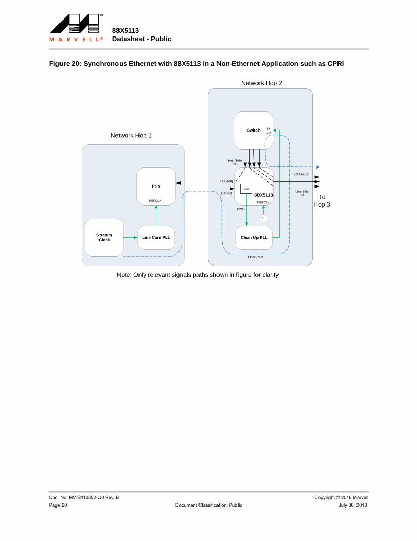
88X5113 Datasheet - Public
Doc. No. MV-S110852-U0 Rev. B Copyright © 2018 Marvell
Page 60 Document Classification: Public July 30, 2018
Figure 20: Synchronous Ethernet with 88X5113 in a Non-Ethernet Application such as CPRI
To Hop 3
StratumClock Line Card PLL
PHY
REFCLK
Clean Up PLL
REFCLK
RCLK
Network Hop 1
Network Hop 2
Clock Path
Switch TXCLK
Host Side RX
Line Side TX
LIP/N[0]
LOP/N[0]
LOP/N[1:3]
CDR
88X5113
Note: Only relevant signals paths shown in figure for clarity

Functional DescriptionSynchronous Ethernet Mode
Copyright © 2018 Marvell Doc. No. MV-S110852-U0 Rev. B
July 30, 2018 Document Classification: Public Page 61
Figure 21: Synchronous Ethernet with 88X5113 in an Ethernet Application
The recovered clock can be chosen from line side or host side, and from lane 0 to lane 3. The device has three methods to send out recovered clock (called RCLK A,B,C). RCLK A is sent to Interrupt pin (INTn). The RCLK B is sent to SCL pin. RCLK C is sent to SDA pin.
Figure 22 shows the registers to configure final recovered clock RCLK A to INTn pin. Register 31.F422 is controlling Line side clock divider 1. Bit 0 will choose 32T clock when set to 1 and choose 40T clock when set to 0. Bit 2:1 will choose clock from lane 0~3. Bit 4 is set to 1 to enable the clock divider 1. Bit 5 will set whether to enable clock divider after SERDES clock is ready (set 1). Bit 15:8 configures the divider ratio for clock divider 1. The divide ratio is 2 to the power of ([15:8] +1).
To Hop 3
StratumClock
Line Card PLL
PHY
REFCLK
Clean Up PLL
REFCLK
RCLK
Network Hop 1
Network Hop 2
Clock Path
Switch TXCLK
Host Side RX
LIP/N[0]
LOP/N[0] LOP/N[1:3]
CDR
88X5113
Note: Only relevant signal paths shown in figure for clarity
Rate Match FIFO
CDR
wr_ptr
rd_ptr

88X5113 Datasheet - Public
Doc. No. MV-S110852-U0 Rev. B Copyright © 2018 Marvell
Page 62 Document Classification: Public July 30, 2018
Figure 22: Multiplexing Scheme for Recovered Clock RCLKA
Register 31.F424 controls the host-side clock divider 1. It has same definition as 31.F422.
Register 31.F423 and 31.F425 control Recovered Clock divider 2 of Line Side and Host side correspondingly.
The Line divider 1 clock and divider 2 clock go through MUX 1 and MUX2 to output two clocks (clock1 and clock2) for top-level. It is controlled by 31.F426.0 and 31.F426.2.
The Host divider 1 clock and divider 2 clock go through MUX1 and MUX2 to output two clocks (clock1 and clock2) for top-level. It is controlled by 31.F426.4 and 31.F426.6.
Line clock1, clock2 and Host clock1, clock2 will go through top-level two-level multiplexes to generate final RCLK A, B or C. Each of them can be chosen from either Line or Host side, either from clock1 or clock2 individually.
SERDESLI[0]
Line Rate/40 for 25GLine Rate/20 for 10GLine Rate/10 for 1G
Line Rate/32 for 25GLine Rate/16 for 10G
n/a for 1G
From LI[1]
From LI[12
From LI[3]
Programmable divide ratio of 2 to 512 (8 bits)Even number only
SERDESHI[0]
Line Rate/40 for 25GLine Rate/20 for 10GLine Rate/10 for 1G
From HI[1]
From HI[12
From HI[3]
RCLK A to INTn
Line Rate/32 for 25GLine Rate/16 for 10G
n/a for 1G
Programmable divide ratio of 2 to 512 (8 bits)Even number only
Maximum output frequency of 50Mhz (limited by i/o cell)
31.F422.031.F422.2:1
1
N = 2 * ( 31.F422.15:8 + 1 )
M = 2 * ( 31.F424.15:8 + 1 )
1
31.F424.031.F424.2:1
Div1
Div2
Div2
Div1
31.F427.0=0, sel Line Div131.F427.0=1, sel Line Div2
31.F427.1=0, sel Host side Div1 31.F427.1=1, sel Host side Div2
31.F427.2=0 select Line31.F427.2=1 select Host
31.F427.3=1 to enable Out
Reg 31.F423.15:8
Reg 31.F425.15:8
31.F426.4=0
31.F426.6=1
31.F426.6=1
31.F426.0=0
31.F426.2=1

Functional DescriptionPower Supplies
Copyright © 2018 Marvell Doc. No. MV-S110852-U0 Rev. B
July 30, 2018 Document Classification: Public Page 63
As shown in Figure 22, 31.F427.3:0 configures the final 4 to 1 selection for RCLK A (to INTn pin). Bit 0 selects Line clock1 or clock2. Bit 1 selects Host clock1 or clock2. Bit 3 choose the clock from Line or Host. Bit 4 is the final clock enable. The controls for RCLK B (to SCL) is 31.F427.7:4. The controls for RCLK C (to SDA) is 31.F427.11:8.
3.12 Power SuppliesThe device requires the following supplies to power the core and I/O.
AVDDL, AVDDH, and AVDDC should be tied together and sourced from the same power supply on the board.
AVDDL: Line SERDES 1.0V supply
AVDDH: Host SERDES 1.0V supply
AVDDC: Common analog 1.0V supply
AVDDT: For 25 MHz PLL and temperature sensor function. 3.3V or 2.5V is required for operation.
Couple AVDDT to VSS if the 25 MHz PLL and the temperature sensor functions are not needed. This pin can be tied together with VDDON or VDDOS with filtering to separate it from the digital supply.
Core 0.9V(Commercial) digital supply
VDDON: Digital I/O supply. For 2.5V or 3.3V operation, the VSEL_N pin should be tied to VSS. For 1.05V, 1.2V, 1.5V, 1.8V operation, the VSEL_N pin should be tied to VDDON. The pins running on the VDDON supply are RESETn, SCL, SDA, TDI, TDO, TCK, TMS, TRSTn, GPIO[3:0].
VDDOS: Digital I/O supply. For 2.5V or 3.3V operation, the VSEL_S pin should be tied to VSS. For 1.05V, 1.2V, 1.5V, and 1.8V operation, the VSEL_S pin should be tied to VDDOS. The pins running on the VDDOS supply are MDC, MDIO, INTn, PHYAD[3:0], CONFIG[2:0], TEST[1:0].

88X5113 Datasheet - Public
Doc. No. MV-S110852-U0 Rev. B Copyright © 2018 Marvell
Page 64 Document Classification: Public July 30, 2018
4 Line Side Description
The line interface comprises four differential input lanes and four differential output lanes. Table 40 lists out what is active for all the modes. The device can be configured to operate in single-port operation or four sub-port operation depending on how many SERDES lanes are used to form the port. Each sub-port’s mode of operation can be configured via Auto-Negotiation or forced mode. Any of the modes shown in Table 40 can be set via forced mode. However, only the modes with the Y in the last column can be configured via Clause 73 Auto-Negotiation. Table 41 shows the register setting required to force a particular mode. Register 3.F000n is used to select the sub-port n. 40 Gbps, 50 Gbps, and 100 Gbps speeds are not supported by sub-ports 1, 2, and 3.
For the purpose of the subsequent discussion, we will refer only to the registers in sub-port 0 unless otherwise noted. The registers in ports 1, 2, and 3 are offset as shown in the Equivalent Registers Between Line and Host Interface table in Section 5 and behave in the same way as sub-port 0. Single-port operation (multi-lane port operation) maps into sub-port 0. That is, sub-port 0 supports all speeds, while sub-port 1, 2, and 3 supports neither 40 Gbps, 50 Gbps, nor 100 Gbps speeds.
The priority for mode selection is listed in decreasing order of priority:
1. If Auto-Negotiation of sub-port 0 is enabled (7.0000.12 = 1) and any capability that requires multiple lanes is advertised (for example, 40 Gbps, 50 Gbps, or 100 Gbps), then operation on sub-ports 1, 2, and 3 are disabled. Registers 3.F000 to 3.F0003 are ignored. Auto-Negotiation will determine the mode to operate. Even if the Auto-Negotiation result in a single-lane operation, sub-ports 1, 2, and 3 will still be disabled.
2. If Auto-Negotiation of sub-port 0 is disabled (7.0000.12 = 0), then register 3.F000 is used to force the mode of operation on sub-port 0. If a capability that requires multiple lanes is selected, then operation on sub-ports 1, 2, and 3 are disabled and registers 3.F001 to 3.F003 are ignored.
3. If neither #1 nor #2 above are in effect, then each sub-port operates independently. If sub-port n Auto-Negotiation is enabled then Auto-Negotiation will determine the mode to operate and register 3.F00n is ignored.
4. If none of the above are in effect, then register 3.F00n will determine the mode of operation.
If Auto-Negotiation is disabled on sub-port n and register 3.F00n selects a mode that requires Clause 72 training, then it is the user’s responsibility to properly set the Auto-Negotiation registers to advertise only the capability that is consistent with the mode requested in register 3.F00n even though register 7.0000.12 is set to 0. The Auto-Negotiation in this case is used only to synchronize the two link partners in order to start the Clause 72 training. As part of the Clause 72 training procedure, the device will automatically initiate Auto-Negotiation even though register 7.0000.12 is set to 0. When Auto-Negotiation completes the device will commence Clause 72 training for the mode selected in register 3.F00n. The device only checks that Auto-Negotiation completes, and does not check whether the resolved capability matches the mode selected in register 3.F00n.
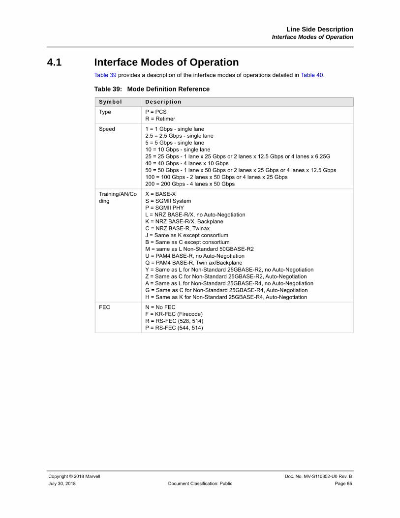
Line Side DescriptionInterface Modes of Operation
Copyright © 2018 Marvell Doc. No. MV-S110852-U0 Rev. B
July 30, 2018 Document Classification: Public Page 65
4.1 Interface Modes of OperationTable 39 provides a description of the interface modes of operations detailed in Table 40.
Table 39: Mode Definition Reference
Symbol Description
Type P = PCSR = Retimer
Speed 1 = 1 Gbps - single lane2.5 = 2.5 Gbps - single lane5 = 5 Gbps - single lane10 = 10 Gbps - single lane25 = 25 Gbps - 1 lane x 25 Gbps or 2 lanes x 12.5 Gbps or 4 lanes x 6.25G40 = 40 Gbps - 4 lanes x 10 Gbps50 = 50 Gbps - 1 lane x 50 Gbps or 2 lanes x 25 Gbps or 4 lanes x 12.5 Gbps100 = 100 Gbps - 2 lanes x 50 Gbps or 4 lanes x 25 Gbps200 = 200 Gbps - 4 lanes x 50 Gbps
Training/AN/Coding
X = BASE-XS = SGMII SystemP = SGMII PHYL = NRZ BASE-R/X, no Auto-NegotiationK = NRZ BASE-R/X, BackplaneC = NRZ BASE-R, TwinaxJ = Same as K except consortiumB = Same as C except consortiumM = same as L Non-Standard 50GBASE-R2U = PAM4 BASE-R, no Auto-NegotiationQ = PAM4 BASE-R, Twin ax/BackplaneY = Same as L for Non-Standard 25GBASE-R2, no Auto-NegotiationZ = Same as C for Non-Standard 25GBASE-R2, Auto-NegotiationA = Same as L for Non-Standard 25GBASE-R4, no Auto-NegotiationG = Same as C for Non-Standard 25GBASE-R4, Auto-NegotiationH = Same as K for Non-Standard 25GBASE-R4, Auto-Negotiation
FEC N = No FECF = KR-FEC (Firecode)R = RS-FEC (528, 514)P = RS-FEC (544, 514)

88X5113 Datasheet - Public
Doc. No. MV-S110852-U0 Rev. B Copyright © 2018 Marvell
Page 66 Document Classification: Public July 30, 2018
Table 40: Interface Modes of Operation Mode Descript ion PCS FEC PMA Autoneg Training Line I /O Mult i-speed
AP Autoneg Resolution
P1X 1000BASE-X 1000BASE-X (CL 36)
None Clause 36 Clause 37/73
None N/A Y
P1S SGMII (System) 1000BASE-X (SGMII)
None Clause 36 SGMII None N/A
P1P SGMII (PHY) 1000BASE-X (SGMII)
None Clause 36 SGMII None N/A
P2.5X 2.5GBASE-X 2.5GBASE-X (* CL 36)
None Clause 361 Clause 732 None CU4HDD1 Y
P5L 5GBASE-R 5GBASE-R (* CL 49)
None Clause 511 Clause 732 None CU4HDD1 Y
P10LN 10GBASE-LR/SR 10GBASE-R (CL 49)
None Clause 51 None None SFI/SFP+
P10KN 10GBASE-KR (No FEC)
10GBASE-R (CL 49)
None Clause 51 Clause 73 CL 72.6.10 KR (CL 72) Y
P10KF 10GBASE-KR (FEC)
10GBASE-R (CL 49)
KR (CL 74)
Clause 51 Clause 73 CL 72.6.10 KR (CL 72) Y
P10LF 10G (Non-standard)
10GBASE-R (CL 49)
KR (CL 74)
Clause 51 None None SFI/SFP+
P25LN 25G (Non-standard) (No FEC)
25GBASE-R (CL 107)
None Clause 109 None None 25GAUI (109A, 109B)
P25LF 25G (Non-standard) (KR-FEC)
25GBASE-R (CL 107)
KR (CL 74)
Clause 109 None None 25GAUI (109A, 109B)
P25LR 25GBASE-SR 25GBASE-R (CL 107)
RS (CL 108)
Clause 109 None None 25GAUI (109A, 109B)
P25CN 25GBASE-CR (No FEC)
25GBASE-R (CL 107)
None Clause 109 Clause 73 CL 72.6.10 CR (CL 110) Y
P25CF 25GBASE-CR (KR-FEC)
25GBASE-R (CL 107)
KR (CL 74)
Clause 109 Clause 73 CL 72.6.10 CR (CL 110) Y
P25CR 25GBASE-CR (RS-FEC)
25GBASE-R (CL 107)
RS (CL 108)
Clause 109 Clause 73 CL 72.6.10 CR (CL 110) Y
P25KN 25GBASE-KR (No FEC)
25GBASE-R (CL 107)
None Clause 109 Clause 73 CL 72.6.10 KR (CL 111) Y
P25KF 25GBASE-KR (KR-FEC)
25GBASE-R (CL 107)
KR (CL 74)
Clause 109 Clause 73 CL 72.6.10 KR (CL 111) Y
P25KR 25GBASE-KR (RS-FEC)
25GBASE-R (CL 107)
RS (CL 108)
Clause 109 Clause 73 CL 72.6.10 KR (CL 111) Y
P25BN 25GBASE-CR (No FEC) (Consortium)
25GBASE-R (CL 107)
None Clause 109 Con OUI CL 72.6.10 CR (CL 110) Y
P25BF 25GBASE-CR (KR-FEC) (Consortium)
25GBASE-R (CL 107)
KR (CL 74)
Clause 109 Con OUI CL 72.6.10 CR (CL 110) Y
P25BR 25GBASE-CR (RS-FEC) (Consortium)
25GBASE-R (CL 107)
RS (CL 108)
Clause 109 Con OUI CL 72.6.10 CR (CL 110) Y

Line Side DescriptionInterface Modes of Operation
Copyright © 2018 Marvell Doc. No. MV-S110852-U0 Rev. B
July 30, 2018 Document Classification: Public Page 67
P25JN 25GBASE-KR (No FEC) (Consortium)
25GBASE-R (CL 107)
None Clause 109 Con OUI CL 72.6.10 KR (CL 111) Y
P25JF 25GBASE-KR (KR-FEC) (Consortium)
25GBASE-R (CL 107)
KR (CL 74)
Clause 109 Con OUI CL 72.6.10 KR (CL 111) Y
P25JR 25GBASE-KR (RS-FEC) (Consortium)
25GBASE-R (CL 107)
RS (CL 108)
Clause 109 Con OUI CL 72.6.10 KR (CL 111) Y
P40LN 40GBASE-LR4/SR4 40GBASE-R4 (CL 82)
None Clause 83 None None XLAUI (CL 83A, 83B)
P40CN 40GBASE-CR4 (No FEC)
40GBASE-R4 (CL 82)
None Clause 83 Clause 73 CL 72.6.10 CR4 (CL 85) Y
P40CF 40GBASE-CR4 (FEC)
40GBASE-R4 (CL 82)
KR (CL 74)
Clause 83 Clause 73 CL 72.6.10 CR4 (CL 85) Y
P40KN 40GBASE-KR4 (No FEC)
40GBASE-R4 (CL 82)
None Clause 83 Clause 73 CL 72.6.10 KR4 (CL 84) Y
P40KF 40GBASE-KR4 (FEC)
40GBASE-R4 (CL 82)
KR (CL 74)
Clause 83 Clause 73 CL 72.6.10 KR4 (CL 84) Y
P40LF 40G (Non-standard)
40GBASE-R4 (CL 82)
KR (CL 74)
Clause 83 None None XLAUI (CL 83A, 83B)
P50LN 50GBASE-LR4/SR4 50GBASE-R4 (CL 82)
None Clause 83 None None XLAUI (CL 83A, 83B)
P50CN 50GBASE-CR4 (No FEC)
50GBASE-R4 (CL 82)
None Clause 83 Clause 734 CL 72.6.10 CR4 (CL 85)
P50CF 50GBASE-CR4 (FEC)
50GBASE-R4 (CL 82)
KR (CL 74)
Clause 83 Clause 734 CL 72.6.10 CR4 (CL 85)
P50KN 50GBASE-KR4 (No FEC)
50GBASE-R4 (CL 82)
None Clause 83 Clause 734 CL 72.6.10 KR4 (CL 84)
P50KF 50GBASE-KR4 (FEC)
50GBASE-R4 (CL 82)
KR (CL 74)
Clause 83 Clause 734 CL 72.6.10 KR4 (CL 84)
P50LF 50G (Non-standard)
50GBASE-R4 (CL 82)
KR (CL 74)
Clause 83 None None XLAUI (CL 83A, 83B)
P50MN 50G (Non-standard) (No FEC)
50GBASE-R2 (CL 82)
None 4:2 (CL 83) None None 2 lane (CL 83A, 83B)
P50MF 50G (Non-standard) (KR-FEC)
50GBASE-R2 (CL 82)
KR (CL 74)
4:2 (CL 83) None None 2 lane (CL 83A, 83B)
P50MR 50G (Non-standard) (RS-FEC)
50GBASE-R2 (CL 82)
RS (Con) 4:2 (CL 83) None None 2 lane (CL 83A, 83B)
P50BN 50GBASE-CR2 (No FEC) (Consortium)
50GBASE-R2 (CL 82)
None 4:2 (CL 83) Con OUI CL 72.6.10 2 lane CR (CL 85)
Y
P50BF 50GBASE-CR2 (KR-FEC) (Consortium)
50GBASE-R2 (CL 82)
KR (CL 74)
4:2 (CL 83) Con OUI CL 72.6.10 2 lane CR (CL 85)
Y
Table 40: Interface Modes of Operation (Continued)
Mode Descript ion PCS FEC PMA Autoneg Training Line I /O Mult i-speed AP Autoneg Resolution

88X5113 Datasheet - Public
Doc. No. MV-S110852-U0 Rev. B Copyright © 2018 Marvell
Page 68 Document Classification: Public July 30, 2018
P50BR 50GBASE-CR2 (RS-FEC) (Consortium)
50GBASE-R2 (CL 82)
RS (Con) 4:2 (CL 83) Con OUI CL 72.6.10 2 lane CR (CL 85)
Y
P50JN 50GBASE-KR2 (No FEC) (Consortium)
50GBASE-R2 (CL 82)
None 4:2 (CL 83) Con OUI CL 72.6.10 2 lane KR (CL 84)
Y
P50JF 50GBASE-KR2 (KR-FEC) (Consortium)
50GBASE-R2 (CL 82)
KR (CL 74)
4:2 (CL 83) Con OUI CL 72.6.10 2 lane KR (CL 84)
Y
P50JR 50GBASE-KR2 (RS-FEC) (Consortium)
50GBASE-R2 (CL 82)
RS (Con) 4:2 (CL 83) Con OUI CL 72.6.10 2 lane KR (CL 84)
Y
P100LN 100GBASE-LR4 100GBASE-R4 (CL 82)
None Clause 83 None None CAUI-4 (CL 83D, 83E)
P100LR 100GBASE-SR4 100GBASE-R4 (CL 82)
RS (CL 91)
Clause 83 None None CAUI-4 (CL 83D, 83E)
P100CR
100GBASE-CR4 100GBASE-R4 (CL 82)
RS (CL 91)
Clause 83 Clause 73 CL 72.6.10 CR4 (CL 92) Y
P100KR
100GBASE-KR4 100GBASE-R4 (CL 82)
RS (CL 91)
Clause 83 Clause 73 CL 72.6.10 KR4 (CL 92) Y
P100KN
100G (Non-standard)
100GBASE-R4 (CL 82)
None Clause 83 Clause 733 CL 72.6.10 KR4 (CL 92)
R1 1G - Transparent 1G - Retimer None None None None N/A
R2.5 2.5G - Transparent 2.5G - Retimer None None Clause 732 None CU4HDD1
R5 5G - Transparent, (No Training)
5G - Retimer None None Clause 732 None CU4HDD1
R10L 10G - Transparent, (No Training)
10G - Retimer None None None None SFI/SFP+
R10K 10G - Transparent, (KR Training)
10G - Retimer None None Clause 73 CL 72.6.10 KR (CL 72)
R25L 25G - Transparent, (No Training)
25G - Retimer None None None None 25GAUI (109A, 109B)
R25C 25G - Transparent, (CR Training)
25G - Retimer None None Clause 73 CL 72.6.10 CR4 (CL 110)
R25K 25G - Transparent, (KR Training)
25G - Retimer None None Clause 73 CL 72.6.10 KR4 (CL 111)
R40L 40G - Transparent, (No Training)
40G - Retimer None None None None XLAUI (CL 83A, 83B)
R40C 40G - Transparent, (CR Training)
40G - Retimer None None Clause 73 CL 72.6.10 CR4 (CL 85)
R40K 40G - Transparent, (KR Training)
40G - Retimer None None Clause 73 CL 72.6.10 KR4 (CL 84)
R100L 100G - Transparent, (No Training)
100G - Retimer None None None None CAUI-4 (CL 83D, 83E)
R100C 100G - Transparent, (CR Training)
100G - Retimer None None Clause 73 CL 72.6.10 CR4 (CL 92)
R100K 100G - Transparent, (KR Training)
100G - Retimer None None Clause 73 CL 72.6.10 KR4 (CL 92)
Table 40: Interface Modes of Operation (Continued)
Mode Descript ion PCS FEC PMA Autoneg Training Line I /O Mult i-speed AP Autoneg Resolution

Line Side DescriptionInterface Modes of Operation
Copyright © 2018 Marvell Doc. No. MV-S110852-U0 Rev. B
July 30, 2018 Document Classification: Public Page 69
Note
• 2.5G and 5G mode currently being defined in IEEE 802.3 CU4HDD study group.
• Clause 73 Auto-Negotiation can be turned on or off. Bits being defined by CU4HDD.
• The P100KN mode is non-standard but requires Auto-Negotiation to be on to start training. The 100GBASE-CR4 bit will be used.
• 50GBASE-R4 uses 40GBASE-R4 Auto-Negotiation ability bits to negotiate. This is a custom mode where both link partners know a-priori to negotiate to 50G
• R400Q uses AN based on Clause 73, with use of allocated next page field for CR-8 and Clause 136 start up protocol for pre-coder/training options.
Table 41: Register Control to Select Mode of Operation
TBD Reimport 3 .F00n.2:01 3.F00n.4 3.F00n.5 3.F00n.7:6 3.F00n.9:8
P1X 1000BASE-X 000 0 1 00 00
P1S SGMII (System) 000 0 1 00 11
P1P SGMII (PHY) 000 0 1 00 10
P2.5X 2.5GBASE-X 001 0 1 00 XX2
P5L 5GBASE-R 010 0 or 1 1 00 XX
P10LN 10GBASE-LR/SR 011 0 1 00 XX
P10KN 10GBASE-KR (No FEC)
011 1 1 00 XX
P10KF 10GBASE-KR (FEC)
011 1 1 01 XX
P10LF 10G (Non-standard)
011 0 1 01 XX
P25LN 25G (Non-standard) (No FEC)
100 0 1 00 XX
P25LF 25G (Non-standard) (KR-FEC)
100 0 1 01 XX
P25LR 25GBASE-SR 100 0 1 10 XX
P25CN 25GBASE-CR (No FEC)
100 1 1 00 00
P25CF 25GBASE-CR (KR-FEC)
100 1 1 01 00
P25CR 25GBASE-CR (RS-FEC)
100 1 1 10 00
P25KN 25GBASE-KR (No FEC)
100 1 1 00 01
P25KF 25GBASE-KR (KR-FEC)
100 1 1 01 01
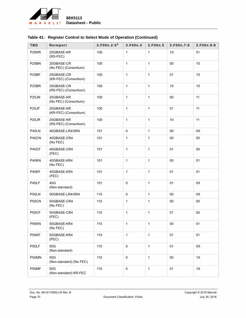
88X5113 Datasheet - Public
Doc. No. MV-S110852-U0 Rev. B Copyright © 2018 Marvell
Page 70 Document Classification: Public July 30, 2018
P25KR 25GBASE-KR (RS-FEC)
100 1 1 10 01
P25BN 25GBASE-CR (No FEC) (Consortium)
100 1 1 00 10
P25BF 25GBASE-CR (KR-FEC) (Consortium)
100 1 1 01 10
P25BR 25GBASE-CR (RS-FEC) (Consortium)
100 1 1 10 10
P25JN 25GBASE-KR (No FEC) (Consortium)
100 1 1 00 11
P25JF 25GBASE-KR (KR-FEC) (Consortium)
100 1 1 01 11
P25JR 25GBASE-KR (RS-FEC) (Consortium)
100 1 1 10 11
P40LN 40GBASE-LR4/SR4 101 0 1 00 0X
P40CN 40GBASE-CR4 (No FEC)
101 1 1 00 00
P40CF 40GBASE-CR4 (FEC)
101 1 1 01 00
P40KN 40GBASE-KR4 (No FEC)
101 1 1 00 01
P40KF 40GBASE-KR4 (FEC)
101 1 1 01 01
P40LF 40G (Non-standard)
101 0 1 01 0X
P50LN 50GBASE-LR4/SR4 110 0 1 00 0X
P50CN 50GBASE-CR4 (No FEC)
110 1 1 00 00
P50CF 50GBASE-CR4 (FEC)
110 1 1 01 00
P50KN 50GBASE-KR4 (No FEC)
110 1 1 00 01
P50KF 50GBASE-KR4 (FEC)
110 1 1 01 01
P50LF 50G (Non-standard)
110 0 1 01 0X
P50MN 50G (Non-standard) (No FEC)
110 0 1 00 1X
P50MF 50G (Non-standard) KR-FEC
110 0 1 01 1X
Table 41: Register Control to Select Mode of Operation (Continued)
TBD Reimport 3 .F00n.2:01 3.F00n.4 3.F00n.5 3.F00n.7:6 3.F00n.9:8

Line Side DescriptionInterface Modes of Operation
Copyright © 2018 Marvell Doc. No. MV-S110852-U0 Rev. B
July 30, 2018 Document Classification: Public Page 71
P50MR 50G (Non-standard) (RS-FEC)
110 0 1 10 1X
P50BN 50GBASE-CR2 (No FEC) (Consortium)
110 1 1 00 10
P50BF 50GBASE-CR2 (KR-FEC) (Consortium)
110 1 1 01 10
P50BR 50GBASE-CR2 (RS-FEC) (Consortium)
110 1 1 10 10
P50JN 50GBASE-KR2 (No FEC) (Consortium)
110 1 1 00 11
P50JF 50GBASE-KR2 (KR-FEC) (Consortium)
110 1 1 01 11
P50JR 50GBASE-KR2 (RS-FEC) (Consortium)
110 1 1 10 11
P100LN 100GBASE-LR4 111 0 1 00 XX
P100LR 100GBASE-SR4 111 0 1 10 XX
P100CR 100GBASE-CR4 111 1 1 10 00
P100KR 100GBASE-KR4 111 1 1 10 01
P100KN 100G (Non-standard)
111 1 1 00 00
1. 3.F00n where n is sub-port n.
2. Where X means don’t care.
Table 41: Register Control to Select Mode of Operation (Continued)
TBD Reimport 3 .F00n.2:01 3.F00n.4 3.F00n.5 3.F00n.7:6 3.F00n.9:8
Table 42: Base Link Register on PCS Modes
88X5113 Base Link Register (3 .x for L ine Side, 4.x for Host Side)
Modes
1G 3001 P1*
2.5G 3001 P2p5**
5G 2001 P5*
10G 2001 P10**
25GR1 2001 P25B/C/J/K/L*
25GR2 1001 P25Y/Z*
25GR4 1001 P25A/G/H*
40GR2 1001 P40B/J*
40GR4 1001 P40C/K/L*
50GR1 1001 P50U/Q*
50GR2 1001 P50B/J/M*

88X5113 Datasheet - Public
Doc. No. MV-S110852-U0 Rev. B Copyright © 2018 Marvell
Page 72 Document Classification: Public July 30, 2018
4.2 Electrical InterfaceThe input of the SERDES (Rx) is AC coupled on die while the output (Tx) is not AC coupled. All SERDES inputs and outputs are internally terminated by 50Ω each (or 100Ω differential).
The SERDES transmitter uses has a three-tap (1 pre-tap and 1 post-tap) FIR filter is implemented for the purpose of channel equalization. The FIR tap values are automatically adjusted during Clause 72 training or can be manually adjusted to optimize the transmit eye over a particular channel.
Table 40 Line I/O column lists out the supported electrical interfaces. Refer to the appropriate standards for detailed information.
4.3 PCS and PMAThe device supports many different modes of operation as shown in Table 40, all the PCS modes reduce down to four PCS types as shown in Table 43. There are four copies of each single-lane PCS types forming four sub-ports and one copy of each multi-lane PCS on sub-port 0. The register location of each PCS type are summarized in the Equivalent Registers Between Line and Host Interface table in Section 5.
50GR4 1001 P50C/K/L*
100GR2 1 P100U/Q*
100GR4 1 P100C/K/L*
200GR4 4001 P200**
NOTE: **The dsp lock for lane 0, 1, 2, and 3 are at registers 0xF201.5, 0xF221.5, 0xF241.5, and 0xF261.
Table 42: Base Link Register on PCS Modes (Continued)
88X5113 Base Link Register (3 .x for L ine Side, 4.x for Host Side)
Modes
Table 43: PCS Types
PCS Mode PCS Type Sub-Port 0 Sub-Port 1 Sub-Port 2 Sub-Port 3
1000BASE-X
1000BASE-X X X X XSGMII PHY
SGMII System
2.5GBASE-X
5GBASE-R
10GBASE-R X X X X10GBASE-R
25GBASE-R
40GBASE-R4
40GBASE-R4 X50GBASE-R4
50GBASE-R2
100GBASE-R4 100GBASE-R4 X

Line Side DescriptionPCS and PMA
Copyright © 2018 Marvell Doc. No. MV-S110852-U0 Rev. B
July 30, 2018 Document Classification: Public Page 73
4.3.1 100GBASE-R4 PCS (Modes P100*)The various 100GBASE-R4 PCS and PMA operate according to IEEE 802.3ba, 802.3bj, and 802.3bm specifications depending on the type selected. In general, a 64B/66B coding and scrambling is used to improve the transmission characteristics of the serial data and ease clock recovery at the receiver. The data stream is distributed across 20 virtual lanes. The alignment markers allows the lanes to be aligned and lanes to be reordered at the receiver. The Reed Solomon FEC reduces the bit error rate of the recovered data.
100GBASE-LR4 up to the CAUI-4 interface takes the path from the CGMII through the 20:4 bit multiplexer to the serializer on the egress direction. It takes the path from the de-serializer though the 4:20 de-multiplexer to the CGMII in the ingress direction. The Reed Solomon FEC is not used and there is no training of the transmitter FIR coefficients.
100GBASE-SR4 up to the CAUI-4 interface takes the path from the CGMII through the transcoder through the Reed Solomon encoder through the symbol distribution to the serializer on the egress direction. The alignment marker is remapped and sent to the Reed Solomon encoder. The receive path starts from the de-serializer through the alignment/de-skew/reorder though the Reed Solomon to the CGMII in the ingress direction. There is no training of the transmitter FIR coefficients. The Reed Solomon uses the RS (528, 514) code.
100GBASE-CR4 (to the CR4 PMD) path is identical to 100GBASE-SR4 except IEEE 802.3 Clause 72.6.10 training occurs to set the transmitter FIR coefficients and the receiver equalization is tuned for shielded balanced copper cabling.
100GBASE-KR4 path is identical to 100GBASE-CR4 except the transmitter FIR and the receiver equalization is tuned for KR4 electrical backplanes.
RS (528, 514). In modes where the Reed Solomon FEC is active, the behavior of the FEC can be modified by setting register 1.00C8.1:0.
00 = Full error detection and correction, set 1.00C8 = 16’h0000.
01 = Error detection without correction. Blocks with errors will be intentionally corrupted to prevent uncorrectable errors from propagating, set 1.00C8 = 16’h0001.
10 = Error detection without correction. Blocks with errors will be passed as received.
The detected error will be reported in registers 1.00CC and 1.00CD.
Each of the bit settings requires a software reset to take effect.
P100KN is a non-standard mode that operates similarly to 100GBASE-LR4 without FEC, but IEEE 802.3 Clause 72.6.10 training occurs. When in this mode, the 100GBASE-CR4 Auto-Negotiation ability is set to initiate the training.

88X5113 Datasheet - Public
Doc. No. MV-S110852-U0 Rev. B Copyright © 2018 Marvell
Page 74 Document Classification: Public July 30, 2018
Figure 23: 100GBASE-R4 Data Path
64/66 Decoder
De-Scrambler
Block Interleaver
Align Marker
Removal
Mux
Block SyncDe-Skew,
Lane Reorder
4:20 Bit De-Mux
Reverse Transcode
Reed Solomon
FEC
Alignment Lock,
De-Skew, Lane
Reorder
BIP Error Calculation
De-Serializer
and Equalizer
64/66 Encoder
ScramblerBlock
Distribution
Alignment Marker
Insertion
20:4 Bit Mux
Transcode
Alignment Marker
Mapping
Reed Solomon Encoder
Symbol Distribution
Mux Serializer
Line Side DescriptionPCS and PMA
Copyright © 2018 Marvell Doc. No. MV-S110852-U0 Rev. B
July 30, 2018 Document Classification: Public Page 75
4.3.2 40GBASE-R4, 50GBASE-R4, 50GBASE-R2 PCS (Modes P40*, P50*) The 40GBASE-R4 PCS operates according to the IEEE 802.3ba specification. The PCS uses a 64B/66B coding and scrambling to improve the transmission characteristics of the serial data and ease clock recovery at the receiver. The data stream is distributed across 4 lanes. The alignment markers allow the lanes to be aligned and lanes to be swapped at the receiver. The synchronization headers for 64B/66B code enable the receiver to achieve block alignment on the receive data.
The 40GBASE-R4 datapath is shown in Figure 24. The Reed-Solomon encoder/FEC path and 4:2 Mux/2:4 De-Mux paths are bypassed in the 40GBASE-R4 and 50GBASE-R4. The differences among the various types are described below.
40GBASE-LR4 up to the XLAUI-4 interface has no training of the transmitter FIR coefficients.
40GBASE-CR4 uses IEEE 802.3 Clause 72.6.10 training to set the transmitter FIR coefficients. The receiver equalization is tuned for shielded balanced copper cabling. The optional Clause 74 KR-FEC can be enabled or disabled.
40GBASE-KR4 path is identical to 40GBASE-CR4 except the transmitter FIR and the receiver equalization is tuned for KR4 electrical backplanes. The optional Clause 74 KR-FEC can be enabled or disabled.
P40LF is a non-standard mode that operates similarly to 40GBASE-LR4 with the KR-FEC enabled. IEEE 802.3 Clause 72.6.10 training does not takes place.
P50L*, P50C*, P50K* modes are identical to each corresponding P40* modes except the line rate is 1.25 times faster.
The 50GBASE-R2 datapath is shown in Figure 24. The path either goes through the Reed-Solomon encoder/FEC path or the 4:2 Mux/2:4 De-Mux paths.
50GBASE-CR2 without FEC and with KR-FEC is similar to 40GBASE-CR4 except the data rate is 1.25 time faster and 4 virtual lanes are bit interleaved onto 2 lanes. This mode uses IEEE 802.3 Clause 72.6.10 training to set the transmitter FIR coefficients. The receiver equalization is tuned for shielded balanced copper cabling.
50GBASE-CR2 with RS-FEC is similar to 40GBASE-CR4 except the data rate is 1.25 times faster and 4 virtual lanes are transcoded and put through the Reed-Solomon encoder. The Reed-Solomon symbols are symbol interleaved onto two lanes. This mode uses IEEE 802.3 Clause 72.6.10 training to set the transmitter FIR coefficients. The receiver equalization is tuned for shielded balanced copper cabling.
50GBASE-KR2 path is identical to 50GBASE-CR2 except the transmitter FIR and the receiver equalization is tuned for KR electrical backplanes.
P50M* modes are identical to each corresponding P50B* modes except IEEE 802.3 Clause 72.6.10 training is not used.

88X5113 Datasheet - Public
Doc. No. MV-S110852-U0 Rev. B Copyright © 2018 Marvell
Page 76 Document Classification: Public July 30, 2018
Figure 24: 40GBASE-R4, 50GBASE-R4, and 50GBASE-R2 Datapath
XLGMII
Scram
bler
Gearbox
KR-ENC Mux
Gearbox
KR-ENC Mux
Gearbox
KR-ENC Mux
Gearbox
KR-ENC Mux
Block D
istribution
Alignm
ent Marker
Insertion
Alignment Marker
Mapping
RS
Encoder
4:2 Mux
Mux
Mux
Transcode Sym
bol D
istribution
Serializer
64/66 Encoder
De-
Ser
ializ
er
2:4
De-
Mux
Mux
Mux
Alig
n Lo
ck, D
e-S
kew
, Reo
rder
Block Sync
KR-FEC
Mux
Block Sync
KR-FEC
Mux
Block Sync
KR-FEC
Mux
Block Sync
KR-FEC
Mux
De-
Ske
w, R
eord
er,
Alig
nmen
t Mar
ker
Rem
oval
RS
FE
C
Rev
erse
T
rans
code
Mux
Blo
ck In
terle
aver
De-
Scr
ambl
er
64/6
6 D
ecod
er
Mux
Mux

Line Side DescriptionPCS and PMA
Copyright © 2018 Marvell Doc. No. MV-S110852-U0 Rev. B
July 30, 2018 Document Classification: Public Page 77
4.3.3 5GBASE-R, 10GBASE-R, and 25GBASE-R PCS (Modes P5L, P10*, P25*)The 10GBASE-R PCS operates according to the IEEE 802.3 Clause 49 specification. The 25GBASE-R PCS operates according to the IEEE 802.3by specification. The PCS uses a 64B/66B coding and scrambling to improve the transmission characteristics of the serial data and ease clock recovery at the receiver.
The 5GBASE-R, 10GBASE-R, and 25GBASE-R datapath is shown in Figure 25.
10GBASE-SR/LR has no training of the transmitter FIR coefficients.
10GBASE-KR uses IEEE 802.3 Clause 72.6.10 training to set the transmitter FIR coefficients. The receiver equalization is tuned for either shielded balanced copper cabling or KR electrical backplanes. The optional Clause 74 KR-FEC can be enabled or disabled.
P10LF is a non-standard mode that operates similarly to 10GBASE-LR with the KR-FEC enabled. IEEE 802.3 Clause 72.6.10 training does not occur.
5GBASE-R is identical to 10GBASE-SR/LR running at half speed.
25GBASE-SR uses the Clause 108 RS-FEC but has no training of the transmitter FIR coefficients.
25GBASE-CR is similar to 25GBASE-SR except it uses IEEE 802.3 Clause 72.6.10 training to set the transmitter FIR coefficients. The receiver equalization is tuned for shielded balanced copper cabling. The optional Clause 74 KR-FEC can be enabled or disabled. The optional Clause 108 RS-FEC can be enabled or disabled.
25GBASE-KR path is identical to 25GBASE-CR except the transmitter FIR and the receiver equalization is tuned for KR electrical backplanes. The optional Clause 74 KR-FEC can be enabled or disabled. The optional Clause 108 RS-FEC can be enabled or disabled.
P25B* modes are identical to each corresponding P25C* modes except the Auto-Negotiation used is per the Consortium specification.
P25J* modes are identical to each corresponding P25K* modes except the Auto-Negotiation used is per the Consortium specification.
P25LN is identical to 10GBASE-SR/LR except running 2.5 times faster.
P25LF is identical to P10LF except running 2.5 times faster.

88X5113 Datasheet - Public
Doc. No. MV-S110852-U0 Rev. B Copyright © 2018 Marvell
Page 78 Document Classification: Public July 30, 2018
Figure 25: 5GBASE-R, 10GBASE-R, and 25GBASE-R Datapath
4.3.4 SGMII, 1000BASE-X, and 2.5GBASE-X
4.3.4.1 PCSThe 1000BASE-X PCS operates according to Clause 36 of the IEEE 802.3 specification. The PCS uses a 8/10 bit coding for DC line balancing. For further details, refer to the IEEE 802.3 specification.
The SGMII protocol is also supported over 1000BASE-X. The SGMII allows 10 Mbps, 100 Mbps, and 1000 Mbps throughput over 1000BASE-X line coding.
When SGMII Auto-Negotiation is turned off (3.3n00.12 = 0), the speed setting is programmed via register 3.3n00 bits 13 and 6. (n = 0, 2, 4, 6 for sub-ports 0, 1, 2, and 3, respectively). Link is established when the underlying 1000BASE-X establishes link.
When SGMII Auto-Negotiation is turned on (3.3n00.12 = 1), the SGMII is set to the speed setting is determined by the Auto-Negotiation speed advertised by the link partner if the device is in SGMII (System) mode. Auto-Negotiations have to complete prior to link being established.
2.500BASE-X is identical to 1000GBASE-X operation as described except it runs 2.5 times faster. Clause 37 Auto-Negotiation is not supported in 2.500BASE-X.
4.3.4.2 1000BASE-X Auto-Negotiation1000BASE-X Auto-Negotiation is defined in Clause 37 of the IEEE 802.3 specification. It is used to auto-negotiate duplex and flow control over fiber cable. Registers 3.3n00, 3.3n04, 3.3n05, 3.3n06, 3.3n07, 3.3n08, and 3.3n0F are used to enable AN, advertise capabilities, determine the link part-ner’s capabilities, show AN status, and show the duplex mode of operation, respectively.
XGMII
Scram
bler
Gearbox
KR-ENC
RS
Encoder
Transcode S
erializer
64/66 Encoder
Mux
De-
Scr
ambl
er
Block Sync
KR-ENC
RS
FE
C
Rev
erse
T
rans
code
De-
Ser
ializ
er
64/6
6 D
ecod
er
Mux
Alig
nmen
t

Line Side DescriptionPCS and PMA
Copyright © 2018 Marvell Doc. No. MV-S110852-U0 Rev. B
July 30, 2018 Document Classification: Public Page 79
The device supports Next Page option for 1000BASE-X Auto-Negotiation. Register 3.3n07 of the fiber pages is used to transmit Next Pages, and register 3.3n08 of the fiber pages is used to store the received Next Pages. The Next Page exchange occurs with software intervention. The user must set register 3.3n04.15 to enable fiber Next Page exchange. Each Next Page received in the regis-ters should be read before a new Next Page to be transmitted is loaded in register 3.3n07.
If the PHY enables 1000BASE-X Auto-Negotiation and the link partner does not, then the link cannot be established. The device implements an Auto-Negotiation bypass mode. See Section 4.3.4.4 for details.
4.3.4.3 SGMII Auto-NegotiationSGMII is a de-facto standard designed by Cisco. SGMII uses 1000BASE-X coding to send data as well as Auto-Negotiation information between the PHY and the MAC. However, the contents of the SGMII Auto-Negotiation are different than the 1000BASE-X Auto-Negotiation. See the Cisco SGMII Specification and the MAC Interfaces and Auto-Negotiation Application Note for further details.
The device supports SGMII interface with and without Auto-Negotiation. Auto-Negotiation can be enabled or disabled by writing to Register 3.3n00.12 followed by a soft reset. If SGMII Auto-Negotiation is disabled, then the MAC interface link, speed, and duplex status (determined by the media side) cannot be conveyed to the MAC from the PHY. The user must program the MAC with this information in some other manner (for example, by reading PHY registers for link, speed, and duplex status).
4.3.4.4 Auto-Negotiation Bypass Mode If the MAC or the PHY implements the Auto-Negotiation function and the other does not implement the function, then two-way communication is not possible unless Auto-Negotiation is manually disabled and both sides are configured to work in the same operational modes. To solve this problem, the device implements the SGMII Interface Auto-Negotiation Bypass Mode. When entering the state Ability_Detect, a bypass timer begins to count down from an initial value of approximately 200 ms. If the device receives idles during the 200 ms, then the device will interpret that the other side is live, but cannot send configuration codes to perform Auto-Negotiation. After 200 ms, the state machine will move to a new state called Bypass_Link_Up in which the device assumes a link-up status and the operational mode is set to the value listed under the Comments column of Table 44.
Table 44: SGMII Auto-Negotiation Modes
Register 3.3n00.12
Register3 .Bn000.13
Comments
0 X No Auto-Negotiation. The user is responsible for determining the speed, link, and duplex status by reading PHY registers.
1 0 Normal SGMII Auto-Negotiation. Speed, link, and duplex status are automatically communicated to the MAC during Auto-Negotiation.
1 1 Media Auto-Negotiation is enabled. Normal operation.
Media Auto-Negotiation is disabled. After 200 ms, the PHY will disable Auto-Negotiation and the link based on idles.

88X5113 Datasheet - Public
Doc. No. MV-S110852-U0 Rev. B Copyright © 2018 Marvell
Page 80 Document Classification: Public July 30, 2018
4.4 Auto-NegotiationThe device supports 802.3ap Clause 73 Auto-Negotiation as well as the next pages required for the 25/50G consortium specifications. When the Auto-Negotiation configuration bits are set correctly and Auto-Negotiation is enabled, no further user intervention is required for Auto-Negotiation to complete.
There are four copies of the Auto-Negotiation circuit on the line interface. Sub-port 0 supports all abilities shown in Table 40 with a Y in the last column. Sub-ports 1, 2, and 3 is similar to sub-port 0 except 40G, 50G, and 100G modes are not supported.
The enabling and disabling of the Auto-Negotiation circuit for each sub-port is discussed in Section 4. If Auto-Negotiation is disabled and the device is manually set to a mode that KR training is required, then Auto-Negotiation will still run automatically. It is the user’s responsibility to properly set the Auto-Negotiation registers to advertise only the capability that is consistent with the manually set mode.
The registers to control the 802.3ap Auto-Negotiation for sub-port 0 can be found starting at register 7.0000. The registers to control sub-port 0 consortium Auto-Negotiation can be found starting at register 7.8010. The registers for sub-port 1, 2, and 3 can be found in their corresponding offset addresses as mapped in the 88X5113 Registers documentation.

Line Side DescriptionLoopback
Copyright © 2018 Marvell Doc. No. MV-S110852-U0 Rev. B
July 30, 2018 Document Classification: Public Page 81
4.5 Loopback
4.5.1 Line-side LoopbacksFigure 26 shows shallow line loopback (path A), deep loopbacks for line side. The deep loopback can be enabled at PCS to PMA boundary which is called PCS deep loopback (path B). The deep loopback can be at PMA to SERDES boundary so called PMA deep loopback (path C).
Table 45 shows how to turn on shallow line loopback. Table 46 shows how to turn on deep loopbacks for line side.
Figure 26: Line-side Loopback
TX PMA
TX PMARX PMA
RX PMA
TX PCS
RX PCS
RX PCS
TX PCS
Host side Line side
ABC
Table 45: Shallow Line Loopback Control Bits
Line Loopback Bits Descript ion Unit Affected Register – Line
1G/2.5G, 5G/10G/25G lane 0, 40G/50G, 100G Lane 0 Set 3.F010.12 = 1 (Loopback A in Figure 26)
1G/2.5G, 5G/10G/25G lane 1 Lane 1 Set 3.F010.13 = 1 (Loopback A in Figure 26)
1G/2.5G, 5G/10G/25G lane 2 Lane 2 Set 3.F010.14 = 1 (Loopback A in Figure 26)
1G/2.5G, 5G/10G/25G lane 3 Lane 3 Set 3.F010.15 = 1 (Loopback A in Figure 26)

88X5113 Datasheet - Public
Doc. No. MV-S110852-U0 Rev. B Copyright © 2018 Marvell
Page 82 Document Classification: Public July 30, 2018
The couple modes such as 40G/50G-R4, 50G-R2, and 100G-R4 always use lane 0.
4.5.2 Host-side LoopbacksFigure 27 shows the paths for shallow host loopback (D), PCS deep loopback (E), and PMA deep loopback (F) for the host side.
Table 47 shows how to turn on a shallow host loopback. Table 48 shows how to turn on deep loopbacks for the host side.
Figure 27: Turn On Deep Host Loopback
Table 46: Deep Loopback Control Bits
Deep Loopback Bits Description
Unit Affected
Register – L ine(PCS Deep Loopback)
Register – L ine (PMA Deep Loopback)
Deep loopback – 100G Lane 0 3.0000.14 (Loopback E in Figure 27) 1.0000.0 (Loopback F in Figure 27)
Deep loopback – 40G/50G
Lane 0 3.1000.14 (Loopback E in Figure 27) 1.2000.0 (Loopback F in Figure 27)
Deep loopback – 5G/10G/25G
Lane 0Lane 1Lane 2Lane 3
3.2000.14 (Loopback E in Figure 27)3.2200.14 3.2400.14 3.2600.11
1.4000.0 (Loopback F in Figure 27)
Deep loopback – 1G/2.5G
Lane 0Lane 1Lane 2Lane 3
3.3000.143.3200.143.3400.14 (Loopback F in Figure 27)3.3600.14
1.6000.0 (Loopback F in Figure 27)
TX PMA
TX PMARX PMA
RX PMA
TX PCS
RX PCS
RX PCS
TX PCS
Host side Line side
Deep Host PCS loopback on line side
towards host100G, 40G, 25G,10G,1G
Deep Host PMA Loopback
Shallow Host Loopback
100G, 40G,25G,10G,1G
D E F

Line Side DescriptionLoopback
Copyright © 2018 Marvell Doc. No. MV-S110852-U0 Rev. B
July 30, 2018 Document Classification: Public Page 83
The couple modes such as 40G/50G-R4, 50G-R2, and 100G-R4 always use lane 0.
Table 47: Shallow Line Loopback Control Bits
Line Loopback Bits Description Unit Affected
Register – L ine
1G/2.5G, 5G/10G/25G lane 0, 40G/50G, 100G Lane 0 Set 4.F010.12 = 1 (Loopback D in Figure 27).
1G/2.5G, 5G/10G/25G lane 1 Lane 1 Set 4.F010.13 = 1 (Loopback D in Figure 27).
1G/2.5G, 5G/10G/25G lane 2 Lane 2 Set 4.F010.14 = 1 (Loopback D in Figure 27).
1G/2.5G, 5G/10G/25G lane 3 Lane 3 Set 4.F010.15 = 1 (Loopback D in Figure 27).
Table 48: Deep Loopback Control Bits
Deep Loopback Bits Descript ion
Unit Affected
Register – Line(PCS Deep Loopback)
Register – L ine (PMA Deep Loopback)
Deep loopback – 100G Lane 0 4.0000.14 (Loopback B in Figure 26) 1.1000.0 (Loopback C in Figure 26)
Deep loopback – 40G/50G Lane 0 4.1000.14 (Loopback B in Figure 26) 1.3000.0 (Loopback C in Figure 26)
Deep loopback – 5G/10G/25G
Lane 0Lane 1Lane 2Lane 3
4.2000.14 4.2200.144.2400.14 (Loopback B in Figure 26)4.2600.11
1.5000.0 (Loopback C in Figure 26)
Deep loopback – 1G/2.5G Lane 0Lane 1Lane 2Lane 3
4.3000.144.3200.144.3400.144.3600.14 (Loopback B in Figure 26)
1.7000.0 (Loopback C in Figure 26)

88X5113 Datasheet - Public
Doc. No. MV-S110852-U0 Rev. B Copyright © 2018 Marvell
Page 84 Document Classification: Public July 30, 2018
4.6 Synchronized FIFOThere is a transmit synchronizing FIFO in all PCS including 1G, 10G, 25G, 40G/50G, and 100G PCS. Each of the FIFOs reconciles the frequency differences between the internal bus clock and the clock used to transmit data onto the media interface. It also buffers the data when inserting Alignment Maker. Each of the FIFOs can support a maximum frame size of 10 KB with up to ±100 PPM clock jitter.
4.7 Traffic Generation and CheckingThere are several packet generator and checkers in the device. There are 22 16-bit registers associated with each generator and checker. This section will refer to these registers as R00 to R21. The register mapping is shown in Table 49.
Table 49: Packet Generator and Checker Register Mapping1 Data
Register Descript ion P100* P40*, P50*
P5*, P10* , P25*
P1*, P2.5*
R00 Packet Generation Control 1 3.8100 3.9010 3.An10 3.Bn10
R01 Packet Generation Control 2 3.8101 3.9011 3.An11 3.Bn11
R02 Initial Payload 0-1/Packet Generation 3.8102 3.9012 3.An12 3.Bn12
R03 Initial Payload 2-3/Packet Generation 3.8103 3.9013 3.An13 3.Bn13
R04 Packet Generation Length 3.8106 3.9016 3.An16 3.Bn16
R05 Packet Generation Burst Sequence 3.8107 3.9017 3.An17 3.Bn17
R06 Packet Generation IPG 3.8108 3.9018 3.An18 3.Bn18
R07 Transmit Packet Counter [15:0] 3.810B 3.901B 3.An1B 3.Bn1B
R08 Transmit Packet Counter [31:16] 3.810C 3.901C 3.An1C 3.Bn1C
R09 Transmit Packet Counter [47:32] 3.810D 3.901D 3.An1D 3.Bn1D
R10 Transmit Byte Counter [15:0] 3.810E 3.901E 3.An1E 3.Bn1E
R11 Transmit Byte Counter [31:16] 3.810F 3.901F 3.An1F 3.Bn1F
R12 Transmit Byte Counter [47:32] 3.8110 3.9020 3.An20 3.Bn20
R13 Receive Packet Counter [15:0] 3.8111 3.9021 3.An21 3.Bn21
R14 Receive Packet Counter [31:16] 3.8112 3.9022 3.An22 3.Bn22
R15 Receive Packet Counter [47:32] 3.8113 3.9023 3.An23 3.Bn23
R16 Receive Byte Count [15:0] 3.8114 3.9024 3.An24 3.Bn24
R17 Receive Byte Count [31:16] 3.8115 3.9025 3.An25 3.Bn25
R18 Receive Byte Count [47:32] 3.8116 3.9026 3.An26 3.Bn26
R19 Receive Packet Error Count [15:0] 3.8117 3.9027 3.An27 3.Bn27

Line Side DescriptionTraffic Generation and Checking
Copyright © 2018 Marvell Doc. No. MV-S110852-U0 Rev. B
July 30, 2018 Document Classification: Public Page 85
The packet generator and packet checker are enabled by separate control bits – R00.0 controls the packet checker and R00.1 controls the packet generator. (Table 50).
When the packet Generator is enabled, packet stream is generated and a pair of 48-bit counters tracks the packet stream. Transmit Packet Counter (R07, R08, and R09) counts number of packets sent. Transmit Byte Counter (R10, R11, and R12) counts number of bytes sent.
Similarly, when the packet checker is enabled, received packets are examined and a set of three 48-bit counters are updated. Received Packet Counter (R13, R14, and R15) counts number of packets received. Received Byte Counter (R16, R17, and R18) counts number of bytes received, and Received Error Counter (R19, R20, and R21) counts number of received packets with CRC error.
R20 Receive Packet Error Count [31:16] 3.8118 3.9028 3.An28 3.Bn28
R21 Receive Packet Error Count [47:32] 3.8119 3.9029 3.An29 3.Bn29
1. N = 0, 2, 4, 6 for sub-ports 0, 1, 2, and 3, respectively.
Table 49: Packet Generator and Checker Register Mapping1 Data (Continued)
Register Descript ion P100* P40*, P50*
P5*, P10* , P25*
P1*, P2.5*
Table 50: Packet Generator and Checker Control and Counters
Register Funct ion Descript ion
R00.0 Enable Packet Checker 1: Packet Checker is enabled. 0: Packet Checker is disabled.
R00.1 Enable Packet Generator 1: Packet Generator is enabled.0: Packet Generator is disabled.
R00.6 Counter reset 1: Clear counters. 0: Normal operation This bit clears itself after counter reset.
R00.15 Counter reset on read 1: Clear the counter as it is read. 0: The counter value is not cleared when it is read.
R07R08R09
Transmit Packet Counter These are the 48-bit Tx packet counters, they are incremented as each packet is sent. A reset of these counters is controlled by the Counter reset bit (R00.6) and the Counter reset on read bit (R00.15) above.
R10R11R12
Transmit Byte Counter These are the 48-bit Tx byte counters, they are incremented as each data byte is sent, including CRC bytes. A reset of these counters is controlled by the Counter reset bit (R00.6) and the Counter reset on read bit (R00.15) above.
R13R14R15
Received Packet Counter These are the 48-bit Rx packet counters, they are incremented as each packet is received.A reset of these counters is controlled by the Counter reset bit (R00.6) and the Counter reset on read bit (R00.15) above.

88X5113 Datasheet - Public
Doc. No. MV-S110852-U0 Rev. B Copyright © 2018 Marvell
Page 86 Document Classification: Public July 30, 2018
4.7.1 Packet GeneratorA packet generator enables the device to generate traffic onto the media without a requirement to receive data from the host.
As a reference, the following depicts the basic structure of Packet Generator output in XLGMII (40G) and CGMII (100G) format.
Figure 28: Packet Format
R16R17R18
Received Byte Counter These are the 48-bit Rx byte counters, they are incremented as each data byte is received, including CRC bytes.A reset of these counters is controlled by the Counter reset bit (R00.6) and the Counter reset on read bit (R00.15) above.
R19R20R21
Received Error Counter These are the 48-bit Rx error counters, they are incremented as each packet is received with a CRC error.A reset of these counters is controlled by the Counter reset bit (R00.6) and the Counter reset on read bit (R00.15) above.
Table 50: Packet Generator and Checker Control and Counters (Continued)
Register Funct ion Descript ion
TXC[7:0] TXD[63:0] Bit 0 is first bit shifted out. Packet starts at CGMII boundary of 64 bit.
01 <sfd> 55 55 55 55 55 55 [S] Lane0 [S] = 0xFB. Lane7 <sfd> = 0xD5
00 (data 7) – (data 0) n bytes of data specified by Packet Length register00
00 (data n-2)
E0 [I] [I] [T] (crc[31:0]) (data n-1) [T] = 0xFD [I] = 0x07

Line Side DescriptionTraffic Generation and Checking
Copyright © 2018 Marvell Doc. No. MV-S110852-U0 Rev. B
July 30, 2018 Document Classification: Public Page 87
Figure 29: Normal CRC Calculation (in XLGMII/40G and CGMII/100G Format)
Figure 30: Extended CRC Calculation (in XLGMII/40G and CGMII/100G Format)
Table 51: Registers Controlling Packet Generation
Register Funct ion Description
R00.1 Enable Packet Generator
1: The packet generator is enabled.0: The packet generator is disabled.
R01.3 R00.2
CRC Disable SFD Enable
CRC,SFD=00: CRC calculation is enabled and CGMII word 0 lane 7 <sfd> = 0xD5. CRC calculation starts after <sfd> byte in packet
CRC,SFD=01: CRC calculation is enabled and CGMII word 0 lane 7 <preA> = 0x55. CRC calculation start after 8th byte in packet
CRC,SFD=11: Extended CRC calculation is enabled and CGMII word 0 lane 7 <preA> = 0x55. Extended CRC calculation starts after [S] byte.NOTE: Extended CRC function is only available in 40G and 100G modes.
CRC,SFD=10: CRC calculation is disabled and CGMII word 0 lane 7 <sfd> = 0xD5.
R04 Packet Length 0x0000: Random length between 64 bytes to 1518 bytes0x0001: Random length between 64 bytes to 0x0FFF bytes0x0002: Random length between 64 bytes to 0x1FFF bytes0x0003: Random length between 64 bytes to 0x3FFF bytes0x0004: Random length between 64 bytes to 0x7FFF bytes0x0005: Random length between 64 bytes to 0xFFFF bytes0x0006 – 0x0007: undefined0x0008 – 0xFFFF = length in number of bytes.
R05 Number of Packets to Generate
0x0000: Stop generation0x0001 – 0xFFFE: number of packets to send0xFFFF = Continuous
<=========== Packet Length ==========>
FB 55 55 55 55 55 55 D5 Data Data n-1 CRC FD 07 07
[S] <====== SFD/PreAmble =====> <========== CRC calculation =========> 0 1 2 3 [T] IPG
(only in 40G and 100G mode) <=========== Packet Length ==========>
FB 55 55 55 55 55 55 55 Data 0 Data n-1 CRC FD 07 07
[S] <========================== CRC calculation =========================> 0 1 2 3 [T] IPG

88X5113 Datasheet - Public
Doc. No. MV-S110852-U0 Rev. B Copyright © 2018 Marvell
Page 88 Document Classification: Public July 30, 2018
Figure 31: Packet without CRC (in XLGMII/40G and CGMII/100G Format)
<=========== Packet Length ==========> End at CGMII word boundary ==>
FB 55 55 55 55 55 55 D5 Data 0 Data n-1 FD 07 07 07 07 07 07
[S] [T] IPG
Table 52: IPG Configuration
Register # Function Description
R06 Inter Packet Gap (IPG)
IPG.15:14 = 00: Fixed number of idle bytes is specified by IPG.13:0For P100*, P50* and P40* modes, IPG is in 8-byte resolution (1 CGMII word). For example:IPG.13:0 = 0x0000 – 0x0007: Next packet starts at the following CGMII word (next 8byte boundary)IPG.13:0 = 0x0008 – 0x000F: After the end of current packet 8-byte boundary, insert 1 CGMII (8 byte) idle before start of next packet.IPG.13:0 = 0x0010 – 0x00017: After the end of current packet 8-byte boundary, insert 2 CGMII (16 byte) idle before start of next packet. For 10G, the resolution is 4 bytes.
IPG.15:14 = 10: Random number of IPG up to the value specified by IPG.13:0
IPG.15:14 = 01: Deficit Idle Count specified by IPG.13:0. Valid IPG.13:0 value is limited to minimum of 8 and maximum of 20.NOTE: Idle Deficit function only available in 40G/50G and 100G modes.
IPG.15:14 = 11: Zero IPG. 1 CGMII word (8 byte) of idle is inserted after n bytes of data, n is specified by IPG.13:0 as following:IPG.13:0 = 0x0080: n = 128 bytesIPG.13:0 = 0x0100: n = 256 bytesIPG.13:0 = 0x0200: n = 512 bytesIPG.13:0 = 0x0400: n = 1024 bytesIPG.13:0 = 0x0800: n = 2048 bytesIPG.13:0 = 0x1000: n = 4096 bytesIPG.13:0 = 0x2000: n = 8196 bytesNOTE: Zero IPG function only available in 40G/50G and 100G modes.
R07R08R09
Transmit Packet Counter
These are the 48-bit Tx packet counters, they are incremented as each packet is sent.
R10R11R12
Transmit Byte Counter
These are the 48-bit Tx byte counters, they are incremented as each data byte is sent, including 4 CRC bytes.

Line Side DescriptionTraffic Generation and Checking
Copyright © 2018 Marvell Doc. No. MV-S110852-U0 Rev. B
July 30, 2018 Document Classification: Public Page 89
Table 53: Packet Data Generation
Register # Funct ion Descript ion
R02R03
Initial Generation
Initial Payload register specifies the initial value of the payload or the fixed value of the payload. The four bytes in this register corresponds to the first 4 bytes of the frame data.
R01 Data Generation
0x0 or 0x1: No mask Value of Initial Payload registers are used as payload repeatedly.
0x2: Invert every other wordValue of Initial Payload registers are used as payload repeatedly but every other CGMII word should be inverted. For example: A payload of 034EA675 will result in a sequence of 034EA675, FCB1598A, 034EA675, FCB1598A, and so on.
0x3: Invert every second wordValue of Initial Payload registers are used as payload repeatedly but inverted every second CGMII word should be inverted. For example: A payload of 034EA675 will result in a sequence of 034EA675, 034EA675, FCB1598A, FCB1598A, 034EA675, 034EA675, and so on.
0x4: Left shift byteValue of Initial Payload registers are used as the initial value and each byte subsequently bitwise left shifted. For example: A payload of 034EA675 will result in a sequence of 034EA675, 069C4DEA, 0C399AD5, 187235AB, and so on.
0x5: Right shift byteValue of Initial Payload registers are used as the initial value and each byte subsequently bitwise right shifted.
0x6: Left shift wordValue of Initial Payload registers are used as the initial value and each 32-bit word subsequently bitwise left shifted. For example: A payload of C34EA675 will result in a sequence of C34EA675, 869D4CEB, 0D3A99D7, 1A7533AE, and so on.
0x7: Right shift wordValue of Initial Payload registers are used as the initial value and each 32-bit word subsequently bitwise right shifted.
0x8: Increment byteValue of Initial Payload registers are used as the initial value and subsequently bytewise incremented. For example: A payload of FFFE0055 will result in a sequence of FFFE0055, 00FF0156, 01000257, 02010358, and so on.
0x9: Decrement byteValue of Initial Payload registers are used as the initial value and subsequently bytewise decremented.
0xA: Pseudo-random byteInitial Payload registers are ignored and a pseudo-random payload is generated. All 4 bytes are the same value for each cycle.
0xB: Pseudo-random wordInitial Payload registers are ignored and a pseudo-random payload is generated. All 4 bytes are randomly generated for each cycle.
0xC – 0xF: Reserved

88X5113 Datasheet - Public
Doc. No. MV-S110852-U0 Rev. B Copyright © 2018 Marvell
Page 90 Document Classification: Public July 30, 2018
4.7.2 Packet Checker
Table 54: Registers Controlling Packet Checker
Register # Function Descript ion
R00.0 Enable Packet Checker
1: Packet Checker is enabled. 0: Packet Checker is disabled.
R01.3 R00.2
CRC disable SFD enable
CRC,SFD=00: CRC calculation is enabled and started after detection of frame delimiter <sfd>
CRC,SFD=01: CRC calculation is enabled and started after eight byte of the packet. The checker assumes the first 8 bytes of packet is the preamble.
CRC,SFD=11: Extended CRC calculation is enabled and started after second byte of the packet.NOTE: Extended CRC function only available in 40G and 100G modes.
CRC,SFD=10: CRC calculation is disabled and data field starts after detection of frame delimited <sfd>
R13R14R15
Received Packet Counter
These are 48-bit Rx packet counters, they are incremented as each packet is received.
R16R17R18
Received Byte Counter
These are 48-bit Rx byte counters, they are incremented as each data byte is received, including 4 CRC bytes.
R19R20R21
Received Error Counter
These are 48-bit Rx error counters, they are incremented as each packet is received with a CRC error.

Line Side DescriptionPRBS Generation and Checking
Copyright © 2018 Marvell Doc. No. MV-S110852-U0 Rev. B
July 30, 2018 Document Classification: Public Page 91
4.8 PRBS Generation and CheckingThe device supports various IEEE defined and proprietary PRBS generators and checkers, and transmit waveform pattern generators. Only one generator and checker may be enabled at a time per lane. Unpredictable results may occur if multiple generators are enabled simultaneously.
4.8.1 General PRBS Generators and Checkers Each lane has its own general PRBS generator and checker. The register definitions for all PRBSs are same except for register offsets. Table 55 shows all PRBS register address offsets. Lane 0 PRBS register address will be used to describe the functionality of PRBS generator and checkers.
To maintain consistency, the address offsets for the host side are listed here.
Register 3.F100 controls the generator and checker. Setting register 3.F100.5 to 1 enables the generator, and setting register 3.F100.4 to 1 enables the checker. If either of these bits is set to 1, then the general PRBS generator and checker overrides the PCS-specific generators and checkers. The port should be set to the selected PCS mode before enabling the PRBS mode to achieve the desired line rate for PRBS testing. When PRBS is enabled, this has higher priority over PCS datapath. Register 3.F100.3:0 controls the pattern that is generated and checked. There is no checker for the high-frequency, low-frequency, mixed-frequency, and square-wave patterns as there are waveforms to check the transmitter performance.
Table 55: PRBS Register Address Offsets
Register Descript ion Line Side Host Side
L0 L1 L2 L3 L0 L1 L2 L3
R0 PRBS control 3.F100 3.F110 3.F120 3.F130 4.F100 4.F110 4.F120 4.F130
R1 R2 R3
Transmit bit counter
3.F1013.F1023.F103
3.F1113.F1123.F113
3.F1213.F1223.F123
3.F1313.F1323.F133
4.F1014.F1024.F103
4.F1114.F1124.F113
4.F1214.F1224.F123
4.F1314.F1324.F133
R4R5R6
Receive bit counter
3.F1043.F1053.F106
3.F1143.F1153.F116
3.F1243.F1253.F126
3.F1343.F1353.F136
4.F1044.F1054.F106
4.F1144.F1154.F116
4.F1244.F1254.F126
4.F1344.F1354.F136
R7R8R9
Receive error counter
3.F1073.F1083.F109
3.F1173.F1183.F119
3.F1273.F1283.F129
3.F1373.F1383.F139
4.F1074.F1084.F109
4.F1174.F1184.F119
4.F1274.F1284.F129
4.F1374.F1384.F139

88X5113 Datasheet - Public
Doc. No. MV-S110852-U0 Rev. B Copyright © 2018 Marvell
Page 92 Document Classification: Public July 30, 2018
All counters are 48 bits long. If register 3.F100.13 is set to 1, then the counters will clear on read. If register 3.F100.13 is set to 0, then the counters continue counting until register 3.F100.6 is set to 1 to clear the contents. If register 3.F100.7 is set to 0, then the PRBS counters will not start to count until the checker first locks onto the incoming PRBS data. If register 3.F100.7 is set to 1, then the PRBS checker will start counting errors without first locking to the incoming PRBS data. Register 3.F100.8 indicates whether the PRBS checker has locked. All 48-bit counters are formed by three 16-bit registers. The lowest addressed register is the least significant 16 bits and the highest addressed register is the most significant 16 bits of the counter. When the least significant register is read, the two upper registers are updated and frozen so that the three register read is atomic. It is not necessary to read the upper registers. However, on subsequent reads of the least significant register, the values of the upper registers from the previous reads are lost. To get the correct upper register value the least significant register must be read first. Register 3.F101, 3.F102, and 3.F103 is the transmit bit counter. Registers 3.F104, 3.F105, and 3.F106 is the receive bit counter. Registers 3.F107, 3.F108, and 3.F109 is the receive bit error counter.
Table 56: Supported Line-side PRBS Patterns
3.F100.3:0 PRBS Pattern Format
0000 IEEE 49.2.8 - PRBS 31
0001 PRBS 7
0010 PRBS 9 IEEE 83.7
0011 PRBS 23
0100 PRBS 31 Inverted
0101 PRBS 7 Inverted
1000 PRBS 15
1001 PRBS 15 Inverted
0110 PRBS 9 Inverted
0111 PRBS 23 Inverted
1010 PRBS 58
1011 PRBS 58 Inverted
1100 PRBS 13
1101 PRBS 13 Inverted
1110 JB03 register addressLane 0 pattern A 3.F10A pattern B 3.F10BLane 1 pattern A 3.F11A pattern B 3.F11BLane 2 pattern A 3.F12A pattern B 3.F12BLane 3 pattern A 3.F13A pattern B 3.F13B
1111 Line-side PRBS square-wave pattern consists of 10 1's followed by 10 0's.

Line Side DescriptionEye Monitor
Copyright © 2018 Marvell Doc. No. MV-S110852-U0 Rev. B
July 30, 2018 Document Classification: Public Page 93
4.8.2 40GBASE-R4-specific Generators and Checkers Register 1.05DD.7 when set to 1 selects PRBS31 pattern. Registers 1.05DD.3 when set to 1 enables Tx generator. Register 1.05DD.0 when set to 1 enables Rx checker. The error counters for individual lanes are in register 1.06A4, 1.06A5, 1.06A6, and 1.06A7, which will be cleared on read.
Register 1.05DD.6 when set to 1 selects PRBS9 pattern. Registers 1.05DD.3 when set to 1 enables Tx generator.
Register 1.05E6.3:0 when set to 1 selects SW (square wave) pattern for individual lanes.
The Line Side Lane 0 to Lane 3 Registers are 3.F100, 3.F110, 3.F120, and 3.F130, respectively.
4.8.3 100GBASE-R4-specific Generators and Checkers Register 1.05DD.7 when set to 1 selects PRBS31 pattern. Registers 1.05DD.3 when set to 1 enables Tx generator. Register 1.05DD.0 when set to 1 enables Rx checker. The error counters for individual lanes are in registers 1.06A4, 1.06A5, 1.06A6, and 1.06A7, which will be cleared on read.
Register 1.05DD.6 when set to 1 selects PRBS9 pattern. Registers 1.05DD.3 when set to 1 enables Tx generator.
Register 1.05E6.3:0 when set to 1 selects SW (square wave) pattern for individual lanes.
Table 57 lists IEEE registers to control PRBS.
4.9 Eye MonitorEach lane has its own non-destructive eye monitor to determine the quality of the received signal in traffic mode.
Table 57: IEEE PCS and PMA PRBS Control Register
Line Side Host S ide
PCS 10G/25G lane 0 3.202A, 3.202B 4.202A, 4.202B
PCS 10G/25G lane 1 3.222A, 3.222B 4.222A, 4.222B
PCS 10G/25G lane 2 3.242A, 3.242B 4.242A, 4.242B
PCS 10G/25G lane 3 3.262A, 3.262B 4.262A, 4.262B
PMA lane 0 1.05DD, 1.05E6, 1.06A4-7 1.15DD, 1.15E6, 1.16A4-7
PMA lane 1 1.25DD, 1.25E6, 1.26A4-7 1.35DD, 1.35E6, 1.36A4-7
PMA lane 2 1.45DD, 1.45E6, 1.46A4-7 1.55DD, 1.55E6, 1.56A4-7
PMA lane 3 1.65DD, 1.65E6, 1.66A4-7 1.75DD, 1.75E6, 1.76A4-7

88X5113 Datasheet - Public
Doc. No. MV-S110852-U0 Rev. B Copyright © 2018 Marvell
Page 94 Document Classification: Public July 30, 2018
5 Host Side Description
The host interface functionality is identical to the line interface in Section 4 with the following exceptions.
The host interface comprises four differential input lanes and four differential output lanes.
All line side registers have equivalent registers in the host side as shown in Table 58. The address either has a different DEVAD or an offset in the REGAD. All the description of the line interface functionality in Section 4 applies to the host interface except for the register address location.
Table 58: Equivalent Registers Between Line and Host Interface
Line Interface Host Interface Description
Start End Start End --
1.0000 1.00FF 1.1000 1.10FF PMA (IEEE) Sub-Port 0
1.2000 1.20FF 1.3000 1.30FF PMA (IEEE) Sub-Port 1
1.4000 1.40FF 1.5000 1.50FF PMA (IEEE) Sub-Port 2
1.6000 1.60FF 1.7000 1.70FF PMA (IEEE) Sub-Port 3
1.8000 1.80FF 1.9000 1.90FF PMA FEC (IEEE) Sub-Port 0
1.0100 1.01FF 1.1100 1.11FF PMA (IEEE) Sub-Port 0
1.2100 1.21FF 1.3100 1.31FF PMA (IEEE) Sub-Port 1
1.4100 1.41FF 1.5100 1.51FF PMA (IEEE) Sub-Port 2
1.6100 1.61FF 1.7100 1.71FF PMA (IEEE) Sub-Port 3
1.8100 1.80FF 1.9100 1.90FF PMA FEC (IEEE) Sub-Port 0
1.0200 1.02FF 1.1200 1.12FF PMA (IEEE) Sub-Port 0
1.2200 1.22FF 1.3200 1.32FF PMA (IEEE) Sub-Port 1
1.4200 1.42FF 1.5200 1.52FF PMA (IEEE) Sub-Port 2
1.6200 1.62FF 1.7200 1.72FF PMA (IEEE) Sub-Port 3
1.0300 1.03FF 1.1300 1.13FF PMA (IEEE) Sub-Port 0
1.2300 1.23FF 1.3300 1.33FF PMA (IEEE) Sub-Port 1
1.4300 1.43FF 1.5300 1.53FF PMA (IEEE) Sub-Port 2
1.6300 1.63FF 1.7300 1.73FF PMA (IEEE) Sub-Port 3
1.0400 1.04FF 1.1400 1.14FF PMA (IEEE) Sub-Port 0
1.2400 1.24FF 1.3400 1.34FF PMA (IEEE) Sub-Port 1

Host Side Description
Copyright © 2018 Marvell Doc. No. MV-S110852-U0 Rev. B
July 30, 2018 Document Classification: Public Page 95
1.4400 1.44FF 1.5400 1.54FF PMA (IEEE) Sub-Port 2
1.6400 1.64FF 1.7400 1.74FF PMA (IEEE) Sub-Port 3
1.0500 1.05FF 1.1500 1.15FF PMA (IEEE) Sub-Port 0
1.2500 1.25FF 1.3500 1.35FF PMA (IEEE) Sub-Port 1
1.4500 1.45FF 1.5500 1.55FF PMA (IEEE) Sub-Port 2
1.6500 1.65FF 1.7500 1.75FF PMA (IEEE) Sub-Port 3
1.0600 1.06FF 1.1600 1.16FF PMA (IEEE) Sub-Port 0
1.2600 1.26FF 1.3600 1.36FF PMA (IEEE) Sub-Port 1
1.4600 1.46FF 1.5600 1.56FF PMA (IEEE) Sub-Port 2
1.6600 1.66FF 1.7600 1.76FF PMA (IEEE) Sub-Port 3
1.C000 1.C0FF 1.D000 1.D0FF PMA (Marvell) Sub-Port 0
1.C200 1.C2FF 1.D200 1.D2FF PMA (Marvell) Sub-Port 1
1.C400 1.C4FF 1.D400 1.D4FF PMA (Marvell) Sub-Port 2
1.C600 1.C6FF 1.D600 1.D6FF PMA (Marvell) Sub-Port 3
1.C800 1.C8FF 1.D800 1.D8FF PMA (Marvell) All ports
1.C100 1.C1FF 1.D100 1.D1FF PMA (Marvell) Sub-Port 0
1.C300 1.C3FF 1.D300 1.D3FF PMA (Marvell) Sub-Port 1
1.C500 1.C5FF 1.D500 1.D5FF PMA (Marvell) Sub-Port 2
1.C700 1.C7FF 1.D700 1.D7FF PMA (Marvell) Sub-Port 3
1.C900 1.C9FF 1.D900 1.D9FF PMA (Marvell) All ports
1.CB00 1.CBFF 1.DB00 1.DBFF PMA (Marvell) All ports
1.CD00 1.CDFF 1.DD00 1.DDFF PMA (Marvell) All ports
1.CF00 1.CFFF 1.DF00 1.DFFF PMA (Marvell) All ports
3.4000 3.40FF 4.4000 4.40FF 200GBASE-R4 (IEEE)
3.4100 3.41FF 4.4100 4.41FF 200GBASE-R4 (IEEE)
3.3000 3.30FF 4.3000 4.30FF 1/2.5GBASE-R (IEEE) Sub-Port 0
3.3200 3.32FF 4.3200 4.32FF 1/2.5GBASE-R (IEEE) Sub-Port 1
3.3400 3.34FF 4.3400 4.34FF 1/2.5GBASE-R (IEEE) Sub-Port 2
Table 58: Equivalent Registers Between Line and Host Interface (Continued)
Line Interface Host Interface Description
Start End Start End --

88X5113 Datasheet - Public
Doc. No. MV-S110852-U0 Rev. B Copyright © 2018 Marvell
Page 96 Document Classification: Public July 30, 2018
3.3600 3.36FF 4.3600 4.36FF 1/2.5GBASE-R (IEEE) Sub-Port 3
3.3100 3.31FF 4.3100 4.31FF 1/2.5GBASE-R (IEEE) Sub-Port 0
3.3300 3.33FF 4.3300 4.33FF 1/2.5GBASE-R (IEEE) Sub-Port 1
3.3500 3.35FF 4.3500 4.35FF 1/2.5GBASE-R (IEEE) Sub-Port 2
3.3700 3.37FF 4.3700 4.37FF 1/2.5GBASE-R (IEEE) Sub-Port 3
3.2000 3.20FF 4.2000 4.20FF 5/10/25GBASE-R (IEEE) Sub-Port 0
3.2200 3.22FF 4.2200 4.22FF 5/10/25GBASE-R (IEEE) Sub-Port 1
3.2400 3.24FF 4.2400 4.24FF 5/10/25GBASE-R (IEEE) Sub-Port 2
3.2600 3.26FF 4.2600 4.26FF 5/10/25GBASE-R (IEEE) Sub-Port 3
3.2100 3.21FF 4.2100 4.21FF 5/10/25GBASE-R (IEEE) Sub-Port 0
3.2310 3.23FF 4.2310 4.23FF 5/10/25GBASE-R (IEEE) Sub-Port 1
3.2500 3.25FF 4.2500 4.25FF 5/10/25GBASE-R (IEEE) Sub-Port 2
3.2700 3.27FF 4.2700 4.27FF 5/10/25GBASE-R (IEEE) Sub-Port 3
3.1000 3.10FF 4.1000 4.10FF 40GBASE-R4 (IEEE) Sub-Port 0
3.1200 3.12FF 4.1200 4.12FF 40GBASE-R4 (IEEE) Sub-Port 1
3.1400 3.14FF 4.1400 4.14FF 40GBASE-R4 (IEEE) Sub-Port 2
3.1600 3.16FF 4.1600 4.16FF 40GBASE-R4 (IEEE) Sub-Port 3
3.1100 3.11FF 4.1100 4.11FF 40GBASE-R4 (IEEE) Sub-Port 0
3.1300 3.13FF 4.1300 4.13FF 40GBASE-R4 (IEEE) Sub-Port 1
3.1500 3.15FF 4.1500 4.15FF 40GBASE-R4 (IEEE) Sub-Port 2
3.1700 3.17FF 4.1700 4.17FF 40GBASE-R4 (IEEE) Sub-Port 3
3.0000 3.00FF 4.0000 4.00FF 100GBASE-R4 (IEEE) sub-port 0
3.0400 3.04FF 4.0400 4.04FF 100GBASE-R4 (IEEE) sub-port 1
3.0500 3.05FF 4.0100 4.01FF 100GBASE-R4 (IEEE) sub-port 0
3.0100 3.05FF 4.0500 4.05FF 100GBASE-R4 (IEEE) sub-port 1
3.0700 3.07FF 4.0700 4.07FF 100GBASE-R4 (IEEE) sub-port 0
3.0B00 3.0BFF 4.0B00 4.0BFF 100GBASE-R4 (IEEE) sub-port 1
3.C000 3.C0FF 4.C000 4.C0FF 200GBASE-R4 (Marvell)
Table 58: Equivalent Registers Between Line and Host Interface (Continued)
Line Interface Host Interface Description
Start End Start End --

Host Side Description
Copyright © 2018 Marvell Doc. No. MV-S110852-U0 Rev. B
July 30, 2018 Document Classification: Public Page 97
3.C100 3.C1FF 4.C100 4.C1FF 200GBASE-R4 (Marvell)
3.B000 3.B0FF 4.B000 4.B0FF 1/2.5GBASE-R (Marvell) Sub-Port 0
3.B200 3.B2FF 4.B200 4.B2FF 1/2.5GBASE-R (Marvell) Sub-Port 1
3.B400 3.B4FF 4.B400 4.B4FF 1/2.5GBASE-R (Marvell) Sub-Port 2
3.B600 3.B6FF 4.B600 4.B6FF 1/2.5GBASE-R (Marvell) Sub-Port 3
3.B100 3.B1FF 4.B100 4.B1FF 1/2.5GBASE-R (Marvell) Sub-Port 0
3.B300 3.B3FF 4.B300 4.B3FF 1/2.5GBASE-R (Marvell) Sub-Port 1
3.B500 3.B5FF 4.B500 4.B5FF 1/2.5GBASE-R (Marvell) Sub-Port 2
3.B700 3.B7FF 4.B700 4.B7FF 1/2.5GBASE-R (Marvell) Sub-Port 3
3.A000 3.A0FF 4.A000 4.A0FF 5/10/25GBASE-R (Marvell) Sub-Port 0
3.A200 3.A2FF 4.A200 4.A2FF 5/10/25GBASE-R (Marvell) Sub-Port 1
3.A400 3.A4FF 4.A400 4.A4FF 5/10/25GBASE-R (Marvell) Sub-Port 2
3.A600 3.A6FF 4.A600 4.A6FF 5/10/25GBASE-R (Marvell) Sub-Port 3
3.A100 3.A1FF 4.A100 4.A1FF 5/10/25GBASE-R (Marvell) Sub-Port 0
3.A300 3.A3FF 4.A300 4.A3FF 5/10/25GBASE-R (Marvell) Sub-Port 1
3.A500 3.A5FF 4.A500 4.A5FF 5/10/25GBASE-R (Marvell) Sub-Port 2
3.A700 3.A7FF 4.A700 4.A7FF 5/10/25GBASE-R (Marvell) Sub-Port 3
3.9000 3.90FF 4.9000 4.90FF 40GBASE-R4 (Marvell) Sub-Port 0
3.9200 3.92FF 4.9200 4.92FF 40GBASE-R4 (Marvell) Sub-Port 1
3.9400 3.94FF 4.9400 4.94FF 40GBASE-R4 (Marvell) Sub-Port 2
3.9600 3.96FF 4.9600 4.96FF 40GBASE-R4 (Marvell) Sub-Port 3
3.9100 3.91FF 4.9100 4.91FF 40GBASE-R4 (Marvell)
3.8000 3.80FF 4.8000 4.80FF 100GBASE-R4 (Marvell)
3.8100 3.81FF 4.8000 4.80FF 100GBASE-R4 (Marvell)
3.F000 3.F0FF 4.F000 4.F0FF Line or Host Common
3.F100 3.F1FF 4.F100 4.F1FF Line or Host Common
7.0000 7.00FF 7.1000 7.10FF AP Auto-Negotiation (IEEE) Sub-Port 0
7.0200 7.02FF 7.1200 7.12FF AP Auto-Negotiation (IEEE) Sub-Port 1
Table 58: Equivalent Registers Between Line and Host Interface (Continued)
Line Interface Host Interface Description
Start End Start End --

88X5113 Datasheet - Public
Doc. No. MV-S110852-U0 Rev. B Copyright © 2018 Marvell
Page 98 Document Classification: Public July 30, 2018
In most cases, the data flow between the line and host are symmetrical and the mode settings for line and host are interchangeable. The configurations shown in Table 59 are not reversible.
The SGMII (PHY) mode is used on the host interface instead of the SGMII (System) mode. When SGMII Auto-Negotiation is turned on (4.3n00.12 = 1, n = 0, 2, 4, 6 for sub-ports 0, 1, 2, 3 respectively), the speed advertised is set by the operational speed of the corresponding sub-port on the line interface.
7.0400 7.04FF 7.1400 7.14FF AP Auto-Negotiation (IEEE) Sub-Port 2
7.0600 7.06FF 7.1600 7.16FF AP Auto-Negotiation (IEEE) Sub-Port 3
7.0100 7.01FF 7.1100 7.11FF AP Auto-Negotiation (IEEE) Sub-Port 0
7.0300 7.03FF 7.1300 7.13FF AP Auto-Negotiation (IEEE) Sub-Port 1
7.0500 7.05FF 7.1500 7.15FF AP Auto-Negotiation (IEEE) Sub-Port 2
7.0700 7.07FF 7.1700 7.17FF AP Auto-Negotiation (IEEE) Sub-Port 3
7.8000 7.80FF 7.9000 7.90FF AP Auto-Negotiation (Marvell) Sub-Port 0
7.8200 7.82FF 7.9200 7.92FF AP Auto-Negotiation (Marvell) Sub-Port 1
7.8400 7.84FF 7.9400 7.94FF AP Auto-Negotiation (Marvell) Sub-Port 2
7.8600 7.86FF 7.9600 7.96FF AP Auto-Negotiation (Marvell) Sub-Port 3
7.8100 7.81FF 7.9100 7.91FF AP Auto-Negotiation (Marvell) Sub-Port 0
7.8300 7.83FF 7.9300 7.93FF AP Auto-Negotiation (Marvell) Sub-Port 1
7.8500 7.85FF 7.9500 7.95FF AP Auto-Negotiation (Marvell) Sub-Port 2
7.8700 7.87FF 7.9700 7.97FF AP Auto-Negotiation (Marvell) Sub-Port 3
30.0000 30.7FFF 30.8000 30.FFFF SERDES Access
Table 58: Equivalent Registers Between Line and Host Interface (Continued)
Line Interface Host Interface Description
Start End Start End --
Table 59: Non-Reversible Mode Combinations
Line Host
P1S P1P
P25* P40*

Chip Bring UpPower Sequencing
Copyright © 2018 Marvell Doc. No. MV-S110852-U0 Rev. B
July 30, 2018 Document Classification: Public Page 99
6 Chip Bring Up
The chip bring up process involves applying power and supplying a clock to the device, hardware resetting and configuring the device, load the firmware either through the EEPROM, or through the MDIO/TWSI slave, and finally configuring the registers and engaging the data path. The firmware will be reset by hardware reset. Firmware requires a reload if a hardware reset is issued.
6.1 Power SequencingVDDON, VDDOS, AVDDL, AVDDH, AVDDC, and DVDD is applied to the device and the 156.25 MHz differential clock is applied to the CLKP/CLKN pins. This device requires no power up sequencing. However, the recommendation is to power up VDDO and AVDDT first, followed by AVDDH/L/C, followed by DVDD.
If the 25 MHz output clock is to be used on the CLK25P/CLK25N pins, then the AVDDT supply should be tied to 3.3V or 2.5V. Otherwise, it should be AC coupled to ground. AVDDT can be combined with VDDON and VDDOS but with a filtering scheme.
After all the power supplies stabilize, the 25 MHz clock will be stable 7 to 10 ms after the 156.25 MHz clock is stable. The 25 MHz clock is not dependent on the state of the RESETn pin.
6.2 Reset and ConfigurationRESETn should be asserted as shown in Section 7.5.3. At the de-assertion of RESETn, hardware configuration values are latched into the device as described in Section 3.3.

88X5113 Datasheet - Public
Doc. No. MV-S110852-U0 Rev. B Copyright © 2018 Marvell
Page 100 Document Classification: Public July 30, 2018
7 Electrical Specifications
7.1 Absolute Maximum Ratings
Table 60: Absolute Maximum Ratings Stresses above those listed in Absolute Maximum Ratings may cause permanent device failure. Functionality at or above these limits is not implied. Exposure to absolute maximum ratings for extended periods may affect device reliability.
Symbol Parameter Min Max Units
VDDAL Power Supply Voltage on AVDDL with respect to VSS -0.5 1.5 V
VDDAH Power Supply Voltage on AVDDH with respect to VSS -0.5 1.5 V
VDDAC Power Supply Voltage on AVDDC with respect to VSS -0.5 1.5 V
VDDAT Power Supply Voltage on AVDDT with respect to VSS -0.5 3.6 V
VDDON Power Supply Voltage on VDDON with respect to VSS -0.5 3.6 V
VDDOS Power Supply Voltage on VDDOS with respect to VSS -0.5 3.6 V
VDD Power Supply Voltage on DVDD with respect to VSS -0.5 1.5 V
TSTORAGE Storage temperature -40 +1251 °C
1. 125°C is only used as bake temperature for not more than 24 hours. Long-term storage (for example, weeks or longer) should be kept at 85°C or lower.

Electrical SpecificationsRecommended Operating Conditions
Copyright © 2018 Marvell Doc. No. MV-S110852-U0 Rev. B
July 30, 2018 Document Classification: Public Page 101
7.2 Recommended Operating Conditions
Table 61: Recommended Operating Conditions (Commercial)
Symbol Parameter Condit ion Min Typ Max Units
VDDAL1 AVDDL Supply For AVDDL 0.95 1.0 1.05 V
VDDAH AVDDH Supply For AVDDH 0.95 1.0 1.05 V
VDDAC AVDDC Supply For AVDDC 0.95 1.0 1.05 V
VDDAT AVDDT Supply 3.3V 3.135 3.3 3.465 V
2.5V 2.375 2.5 2.625
VVDDO VDDON or VDDOS Supply 3.3V 3.135 3.3 3.465 V
2.5V 2.375 2.5 2.625
1.8V 1.71 1.8 1.89
1.2V 1.14 1.2 1.26
1.05V 0.998 1.05 1.103
VDD DVDD Supply (C Temp) – 0.855 0.9 0.945 V
VDD DVDD Supply (I Temp) – 0.902 0.95 0.997 V
TJ Maximum junction temperature
– – – 1052 °C
1. Maximum noise allowed on supplies is 5 mVppd.
2. Refer to the white paper on TJ Thermal Calculations for detailed information.

88X5113 Datasheet - Public
Doc. No. MV-S110852-U0 Rev. B Copyright © 2018 Marvell
Page 102 Document Classification: Public July 30, 2018
7.3 Package Thermal Information
7.3.1 Thermal Conditions for 169-pin, FCBGA Package
Table 62: Thermal Conditions for 169-pin, FCBGA Package Symbol Parameter Condition Min Typ Max Units
θJA Thermal resistance1 - junction to ambient for the 169-pin FCBGA package
θJA = (TJ - TA)/PP = Total power dissipation
JEDEC 3 in. x 4.5 in. 12-layer PCB with no air flow
– 16.28 – °C/W
JEDEC 3 in. x 4.5 in. 12-layer PCB with 1 meter/sec air flow
– 14.00 – °C/W
JEDEC 3 in. x 4.5 in. 12-layer PCB with 2 meter/sec air flow
– 12.98 – °C/W
JEDEC 3 in. x 4.5 in. 12-layer PCB with 3 meter/sec air flow
– 12.36 – °C/W
ψJT Thermal characteristic parametera - junction to top center of the 169-pin FCBGA package
ψJT = (TJ - Ttop)/PP = Total power dissipation, Ttop: Temperature on the top center of the package
JEDEC 3 in. x 4.5 in. 12-layer PCB with no air flow
– 1.30 – °C/W
JEDEC 3 in. x 4.5 in. 12-layer PCB with 1 meter/sec air flow
– 1.31 – °C/W
JEDEC 3 in. x 4.5 in. 12-layer PCB with 2 meter/sec air flow
– 1.32 – °C/W
JEDEC 3 in. x 4.5 in. 12-layer PCB with 3 meter/sec air flow
– 1.33 – °C/W
θJC Thermal resistancea - junction to case for the 169-pin FCBGA package
θJC = (TJ - TC)/PtopPtop = Power dissipation from the top of the package
JEDEC with no air flow – 1.70 – °C/W
θJB Thermal resistancea - junction to board for the 169-pin FCBGA package
θJB = (TJ - TB)/PbottomPbottom = Power dissipation from the bottom of the package to the PCB surface
JEDEC with no air flow – 5.81 – °C/W
1. Refer to the white paper on TJ Thermal Calculations for detailed information.

Electrical SpecificationsCurrent Consumption
Copyright © 2018 Marvell Doc. No. MV-S110852-U0 Rev. B
July 30, 2018 Document Classification: Public Page 103
7.4 Current Consumption
7.4.1 88X5113 Current Consumption (Commercial)
Example: P100LN to P100CR operation
Current consumption on DVDD = DVDD Base + P100LN + P100CR
Table 63: DVDD Current Consumption
Pins Parameter Condition Min Typ Max Units
DVDD Base Chip Base Power including leakage
– 84 941 mA
1G PCS (1 lane power) P1X, P1S, P1P – 6 8 mA
2.5G PCS (1 lane power) P2.5X – 13 16 mA
5G PCS (1 lane power) P5L, P5K – 13 13 mA
10G PCS - No FEC (1 lane power) P10LN, P10KN – 26 29 mA
10G PCS - KR FEC (1 lane power) P10KF, P10LF – 31 37 mA
25G PCS - No FEC (1 lane power) P25LN, P25LR, P25CN, P25KN, P25BN, P25JN
– 54 60 mA
25G PCS - KR FEC (1 lane power) P25LF, P25CF, P25KF, P25BF, P25JF
– 67 76 mA
25G PCS - RS FEC (1 lane power) P25LR, P25CR, P25KR, P25BR, P25JR
– 99 111 mA
40G PCS - No FEC (4 lane power) P40LN, P40CN, P40KN – 97 109 mA
40G PCS - KR FEC (4 lane power) P40CF, P40KL, P40LF – 119 135 mA
50G PCS - No FEC (4 lane power) P50LN, P50CN, P50KN – 110 124 mA
50G PCS - KR FEC (4 lane power) P50CF, P50KF, P50LF – 139 160 mA
50G PCS - No FEC (2 lane power) P50MN, P50BN, P50JN – 107 122 mA
50G PCS - KR FEC (2 lane power) P50MF, P50BF, P50JF – 120 135 mA
50G PCS - RS FEC (2 lane power) P50MR, P50BR, P50JR – 221 231 mA
100G PCS - No FEC (4 lane power) P100LN, P100KN – 228 263 mA
100G PCS - RS FEC (4 lane power) P100LR, P100CR, P100KR – 430 481 mA

88X5113 Datasheet - Public
Doc. No. MV-S110852-U0 Rev. B Copyright © 2018 Marvell
Page 104 Document Classification: Public July 30, 2018
Example: P100LN to P100CR operation
Current consumption on AVDD = AVDDL Base + AVDDH Base + P100* + P100* + AVDDC
Table 64: AVDDL and AVDDH Current Consumption
Pins Parameter Condit ion Min Typ Max Units
AVDDLorAVDDH
Base Chip Base Power including leakage – 54 350 mA
1G Speed (1 lane power) P1*, R1 – 74 90 mA
2.5G Spkvban641eed (1 lane power)
P2.5X, R2.5 – 89 111 mA
5G Speed (1 lane power) P5*, R5* – 106 125 mA
10G Speed (1 lane power) P10*, R10* – 144 164 mA
25G Speed (1 lane power) P25*, R25* – 256 292 mA
40G Speed (4 lane power) P40*, R40* – 567 653 mA
50G Speed (4 lane power) P50L*, P50C*, P50K* – 641 739 mA
50G Speed (2 lane power) P50M*, P50B*, P50J* – 509 583 mA
100G Speed (4 lane power) P100*, R100* – 1003 1156 mA
Table 65: AVDDC and AVDDT Current Consumption
Pins Parameter Condition Min Typ Max Units
AVDDC Base Chip Base Power including leakage – – 10 mA
AVDDT Base Chip Base Power including leakage – – 34 mA

Electrical SpecificationsCurrent Consumption
Copyright © 2018 Marvell Doc. No. MV-S110852-U0 Rev. B
July 30, 2018 Document Classification: Public Page 105
7.4.2 88X5113 Current Consumption (Industrial)
Example: P100LN to P100CR operation
Current consumption on DVDD = DVDD Base + P100LN + P100CR
Table 66: DVDD Current Consumption
Pins Parameter Condition Min Typ Max Units
DVDD Base Chip Base Power including leakage
– 84 941 mA
1G PCS (1 lane power) P1X, P1S, P1P – 6 8 mA
2.5G PCS (1 lane power) P2.5X – 13 16 mA
5G PCS (1 lane power) P5L, P5K – 13 13 mA
10G PCS - No FEC (1 lane power) P10LN, P10KN – 26 29 mA
10G PCS - KR FEC (1 lane power) P10KF, P10LF – 31 37 mA
25G PCS - No FEC (1 lane power) P25LN, P25LR, P25CN, P25KN, P25BN, P25JN
– 54 60 mA
25G PCS - KR FEC (1 lane power) P25LF, P25CF, P25KF, P25BF, P25JF
– 67 76 mA
25G PCS - RS FEC (1 lane power) P25LR, P25CR, P25KR, P25BR, P25JR
– 99 111 mA
40G PCS - No FEC (4 lane power) P40LN, P40CN, P40KN – 97 109 mA
40G PCS - KR FEC (4 lane power) P40CF, P40KL, P40LF – 119 135 mA
50G PCS - No FEC (4 lane power) P50LN, P50CN, P50KN – 110 124 mA
50G PCS - KR FEC (4 lane power) P50CF, P50KF, P50LF – 139 160 mA
50G PCS - No FEC (2 lane power) P50MN, P50BN, P50JN – 107 122 mA
50G PCS - KR FEC (2 lane power) P50MF, P50BF, P50JF – 120 135 mA
50G PCS - RS FEC (2 lane power) P50MR, P50BR, P50JR – 221 231 mA
100G PCS - No FEC (4 lane power) P100LN, P100KN – 228 263 mA
100G PCS - RS FEC (4 lane power) P100LR, P100CR, P100KR – 430 481 mA

88X5113 Datasheet - Public
Doc. No. MV-S110852-U0 Rev. B Copyright © 2018 Marvell
Page 106 Document Classification: Public July 30, 2018
Example: P100LN to P100CR operation
Current consumption on AVDD = AVDDL Base + AVDDH Base + P100* + P100* + AVDDC
Table 67: AVDDL and AVDDH Current Consumption
Pins Parameter Condit ion Min Typ Max Units
AVDDLorAVDDH
Base Chip Base Power including leakage – 54 350 mA
1G Speed (1 lane power) P1*, R1 – 74 90 mA
2.5G Spkvban641eed (1 lane power)
P2.5X, R2.5 – 89 111 mA
5G Speed (1 lane power) P5*, R5* – 106 125 mA
10G Speed (1 lane power) P10*, R10* – 144 164 mA
25G Speed (1 lane power) P25*, R25* – 256 292 mA
40G Speed (4 lane power) P40*, R40* – 567 653 mA
50G Speed (4 lane power) P50L*, P50C*, P50K* – 641 739 mA
50G Speed (2 lane power) P50M*, P50B*, P50J* – 509 583 mA
100G Speed (4 lane power) P100*, R100* – 1003 1156 mA

Electrical SpecificationsDigital I/O Electrical Specifications
Copyright © 2018 Marvell Doc. No. MV-S110852-U0 Rev. B
July 30, 2018 Document Classification: Public Page 107
7.5 Digital I/O Electrical Specifications
7.5.1 DC Operating Conditions
Table 68: AVDDC and AVDDT Current Consumption
Pins Parameter Condit ion Min Typ Max Units
AVDDC Base Chip Base Power including leakage – – 10 mA
AVDDT Base Chip Base Power including leakage – – 34 mA
Table 69: DC Operating Conditions(Over full range of values listed in the Recommended Operating Conditions unless otherwise specified)
Symbol Parameter Pins Condition Min Typ Max Units
VIH Input High Voltage
All digital inputs VDDO* = 3.3V 2.0 – VDDO + 0.3V
V
VDDO* = 2.5V 1.75 – VDDO + 0.3V
V
VDDO* = 1.8V 1.26 – VDDO + 0.3V
V
VDDO* = 1.5V 1.05 – VDDO + 0.3V
V
VDDO* = 1.2V 0.84 – VDDO + 0.3V
V
VDDO* = 1.05V 0.74 – VDDO + 0.3V
V
VIL Input Low Voltage
All digital inputs VDDO* = 3.3V -0.3 – 0.8 V
VDDO* = 2.5V -0.3 – 0.75 V
VDDO* = 1.8V -0.3 – 0.54 V
VDDO* = 1.5V -0.3 – 0.45 V
VDDO* = 1.2V -0.3 – 0.36 V
VDDO* = 1.05V -0.3 – 0.31 V
VOH High-level Output Voltage
All digital outputs IOH = -4 mA VDDO - 0.4V
– – V
VOL Low-level Output Voltage
All digital outputs IOL = 4 mA – – 0.4 V

88X5113 Datasheet - Public
Doc. No. MV-S110852-U0 Rev. B Copyright © 2018 Marvell
Page 108 Document Classification: Public July 30, 2018
7.5.2 AC Operating Conditions
7.5.3 Reset Timing
Figure 32: Reset Timing
IILK Input Leakage Current
With internal pull-up/pull-down resistor
– 10 – 70 μA
All others without resistor
– – – 10 μA
CIN Input Capacitance
All pins – – – 5 pF
Table 69: DC Operating Conditions(Over full range of values listed in the Recommended Operating Conditions unless otherwise specified)
Symbol Parameter Pins Condition Min Typ Max Units
Table 70: AC Operating Conditions (Over Full range of values listed in the Recommended Operating Conditions unless otherwise specified)
Symbol Parameter Pins Condit ion Min Typ Max Units
TR Rise Time GPIO[0] 20 to 80% of Vppd – 0.87 – ns
TF Fall Time GPIO[0] 20 to 80% of Vppd – 0.68 – ns
Table 71: Reset Timing (Over Full range of values listed in the Recommended Operating Conditions unless otherwise specified)
Symbol Parameter Condit ion Min Typ Max Units
TPU_RESET Valid Power to RESETDe-asserted
– 10 – – ms
TSU_CLK Number of Valid CLK Cycles Prior to RESETDe-asserted
– 50 – – clks
TRESET Minimum Reset Pulse Width During Normal Operation
– 10 – – ms
Power
CLKP/N
RESETn
TPU_RESET
TSU_CLK
TRESET

Electrical SpecificationsDigital I/O Electrical Specifications
Copyright © 2018 Marvell Doc. No. MV-S110852-U0 Rev. B
July 30, 2018 Document Classification: Public Page 109
7.5.4 MDC/MDIO Management Interface Timing
Figure 33: MDC/MDIO Management Interface
Table 72: MDC/MDIO Management Interface Timing (Over full range of values listed in the Recommended Operating Conditions unless otherwise specified)
Symbol Parameter Condition Min Typ Max Units
TDLY_MDIO MDC to MDIO (Output) Delay Time
25 pf load on MDIO 3.5 – 19 ns
TSU_ MDIO MDIO (Input) to MDC Setup Time
– 6.5 – – ns
THD_ MDIO MDIO (Input) to MDC Hold Time
– 0.5 – – ns
TP_ MDC MDC Period Subject to TREAD_DLY 401, 2
1. TP_MDC is minimum of 25 ns for 40 MHz MDC clock support with stretched TA, but 40 ns (25 MHz) with standard TA as per IEEE specification. MDC of 40 MHz is supported only with VDDO supply of 1.8V and above. For lower VDDO, MDC frequency of up to 25 MHz is supported.
2. The maximum MDC frequency is dependent on the Reference Clock used (CLK1P/N). The TP_MDC listed is based on 156.25 MHz reference clock.
– – ns
TH_ MDC MDC High – 12 – – ns
TL_ MDC MDC Low – 12 – – ns
TREAD_DLY Two MDC Period During Read Turnaround
– 80 – – ns
Valid Data
MDCTHD_MDIOTSU_MDIO
MDCTP_MDC TDLY_MDIO
MDIO (Output)
MDIO (Input)
TH_MDC TL_MDC

88X5113 Datasheet - Public
Doc. No. MV-S110852-U0 Rev. B Copyright © 2018 Marvell
Page 110 Document Classification: Public July 30, 2018
7.5.5 JTAG Timing
Figure 34: JTAG Timing
Table 73: JTAG Timing (Over full range of values listed in the Recommended Operating Conditions unless otherwise specified)
Symbol Parameter Condit ion Min Typ Max Units
TP_TCK TCK Period – 60 – – ns
TH_TCK TCK High – 12 – – ns
TL_TCK TCK Low – 12 – – ns
TSU_TDI TDI, TMS-to-TCK Setup Time
– 10 – – ns
THD_TDI TDI, TMS-to-TCK Hold Time – 10 – – ns
TDLY_TDO TCK-to-TDO Delay – 0 – 15 ns
TCK
TDO
TDLY_TDO
TSU_TDI THD_TDI
TH_TCKTL_TCK
TMSTDI
TP_TCK

Electrical SpecificationsSERDES Electrical Specifications
Copyright © 2018 Marvell Doc. No. MV-S110852-U0 Rev. B
July 30, 2018 Document Classification: Public Page 111
7.6 SERDES Electrical Specifications
7.6.1 Chip-to-Module 100 Gbps/25 Gbps Electrical Characteristics
7.6.1.1 Chip-to-Module 100 Gbps/25 Gbps Transmitter and Receiver Characteristics
Table 74: Chip-to-Module CAUI-4/XXVAUI-1 Transmitter and Receiver Characteristics
Symbol Description Min Max Units Notes
BR Baud rate 25.78125 Gbps –
Bppm Baud rate tolerance -100 100 ppm 1
UI Unit interval 38.787879 ps –
Transmitter Parameters
Vodis Transmitter disabled output differential noise level – 35 mV –
Vodpp Output differential maximum peak-to-peak – 900 mV –
Tr Output transition time 10 – ps 8
Vosdc DC Common-mode voltage limits -0.3 2.8 V –
Vosac AC Common-mode voltage limits (RMS) – 17.5 mV –
RLOD Return loss differential output – – dB 2, 4
RLOCD Common to differential mode output return loss See note #3. dB 3, 4
Ehatx Differential output eye height A 95 – mV 10
Ehbtx Differential output eye height B 80 – mV 10
Ew tx Differential output eye width 0.46 – UI 5, 10
Receiver Parameters
Vidpp Input differential voltage – 900 mV 7, 11
RLID Return loss differential input See note #2. dB 2, 4
RLIDC Differential to common mode input return loss See note #3. dB 3, 4
Ehrx Receiver stress tolerance -eye height 228 – mV 5, 6, 11
Ew rx Receiver stress tolerance -eye width 0.57 – UI 5, 6, 11

88X5113 Datasheet - Public
Doc. No. MV-S110852-U0 Rev. B Copyright © 2018 Marvell
Page 112 Document Classification: Public July 30, 2018
Note
The load is 100Ω differential for these parameters, unless otherwise specified. The Tx table is defined on TP1a and Rx table is defined on TP4a refer to 83E.2 CAUI-4 chip-to-module compliance point definitions in the IEEE 802.3 standard. • Defines the allowable reference clock difference and Rx baud rate tolerance relative to
nominal. Tx baud rate is derived from multiplication of the reference clock(0ppmdelta). • RLOD and RLID are defined accordingly: For 10 MHz -8 GHz RLOD/RLID>9.5-0.37*f
[dB] (Frequency defined in GHz). For 8 GHz -19 GHz RLOD/RLID>4.75-7.4Log(f/14) [dB] (Frequency defined in GHz).
• RLOCD and RLID Care defined accordingly: For 10 MHz -12.89 GHz RLOCD/RLIDC>22-(20/25.78)*f [dB] (Frequency defined in GHz). For 12.89 GHz -19 GHz RLOCD/RLIDC>15-(6/25.78)*f [dB] (Frequency defined in GHz).
• Relative to 100Ω differential and 25Ω common mode. • Defined with a Bit Error Rate (BER) of 10^-15. • Defined according to IEEE 802.3 section 83E.3.3.2 Host stressed input test. • Vidpp refers to the peak-to-peak. • Defined 20 to 80% of the signal. Refer to section 83E.3.1.5 Transition time in the
IEEE 802.3 standard. • Refer to section 83E.3.1.4 Differential termination mismatch in IEEE 802.3 standard. • Refer to section 83E.3.1.6 Host output eye width and eye height in IEEE 802.3 standard. Defined on TP4 as defined in 83E.2 CAUI-4 chip-to-module compliance point definitions in IEEE 802.3 standard.
Table 75: Chip-to-Module CAUI-4/XXVAUI-1 Settings and Configuration
Parameter Setting/Configurat ion
Vods The Vods is the output differential amplitude configurable range.When driving a test load, the minimum value is achieved with AMP=TBD and PRE=TBD, and the maximum value is achieved with AMP=TBD and PRE=TBD. Output amplitude and pre-emphasis are configurable.
Viddp The Viddp is the input differential voltage.The maximum single-ended voltage (common mode voltage and swing voltage) must not exceed 1.8V.
Vodpp To achieve the specifications at Tp1a, the use of emphasis may be needed.
Output Equalization
For emphasis control information, refer to the Functional Specifications.
NOTE: For further information, refer to the Functional Specifications.
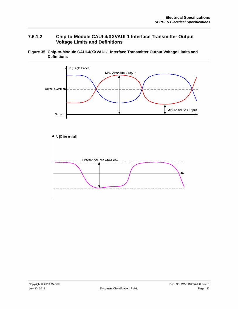
Electrical SpecificationsSERDES Electrical Specifications
Copyright © 2018 Marvell Doc. No. MV-S110852-U0 Rev. B
July 30, 2018 Document Classification: Public Page 113
7.6.1.2 Chip-to-Module CAUI-4/XXVAUI-1 Interface Transmitter Output Voltage Limits and Definitions
Figure 35: Chip-to-Module CAUI-4/XXVAUI-1 Interface Transmitter Output Voltage Limits and Definitions

88X5113 Datasheet - Public
Doc. No. MV-S110852-U0 Rev. B Copyright © 2018 Marvell
Page 114 Document Classification: Public July 30, 2018
Figure 36: Chip-to-Module CAUI-4/XXVAUI-1 Transmitter Output Differential Amplitude and Eye Opening

Electrical SpecificationsSERDES Electrical Specifications
Copyright © 2018 Marvell Doc. No. MV-S110852-U0 Rev. B
July 30, 2018 Document Classification: Public Page 115
7.6.2 Chip-to-Chip 100 Gbps/25 Gbps (CAUI-4/XXVAUI-1) Electrical Characteristics
7.6.2.1 Chip-to-Chip 100 Gbps/25 Gbps (CAUI-4/XXVAUI-1) Transmitter and Receiver Characteristics
Table 76: Chip-to-Chip Gbps CAUI-4/XXVAUI-1 Interface Transmitter and Receiver Characteristics
Symbol Descript ion Min Max Units Notes
BR Baud rate 25.78125 Gbps –
Bppm Baud rate tolerance -100 100 ppm 1
UI Unit interval 38.787879 ps –
Transmitter Parameters
Vodis Transmitter disabled output differential noise level – 30 mV –
Vodpp Output differential maximum peak-to-peak – 1200 mV –
Vf Output waveform -Steady-state voltage 0.4 0.6 V 12
Vlfpp Output waveform -Linear fit pulse peak 0.71*Vf – V 12
Prec Output waveform -Pre-cursor full-scale range See note #13. – 13
Pstc Output waveform - Post-cursor full-scale range See note #13. – 13
Vsnr Transmitter signal-to-noise-and-distortion ratio 27 – dB 14
Vosdc DC Common-mode voltage limits 0.0 1.9 V –
Vosac AC Common-mode voltage limits (RMS) – 12 mV –
RLOD Return loss differential output See note #2. dB 2, 5
RLOC Return loss Common-Mode output See note #3. dB 3, 5
Juctx Output jitter -Effective bounded uncorrelated, peak-to-peak – 0.1 UI 10
Jeotx Output Even-Odd jitter – 0.035 UI 11
Jtpptx Output jitter -Effective total uncorrelated, peak-to-peak – 0.26 UI 6, 9, 10
Receiver Parameters
Vidpp Input differential voltage – 1200 mV 8
RLID Return loss differential input See note #2. dB 2, 5
RLIDC Differential to common mode input return loss See note #4. dB 4, 5
Rit Receiver interference tolerance See note #7. UI 7

88X5113 Datasheet - Public
Doc. No. MV-S110852-U0 Rev. B Copyright © 2018 Marvell
Page 116 Document Classification: Public July 30, 2018
Note
The load is 100Ω differential for these parameters, unless otherwise specified. General Comment: The Tx table is defined on TP0a as defined in 93.8.1.1 Transmitter test fixture in IEEE 802.3 standard. General Comment: The Rx table is defined on TP5a as defined in 93.8.2.1 Receiver test fixture in 802.3 IEEE standard. • Defines the allowable reference clock difference and Rx baud rate tolerance relative
to nominal. Tx baud rate is derived from multiplication of the reference clock (0 ppm delta).
• RLOD and RLID are defined accordingly: For 50 MHz - 6 GHz RLOD/RLID>12.05-f [dB] (Frequency defined in GHz). For 6 GHz -19 GHz RLOD/RLID>6.5-0.075*f [dB] (Frequency defined in GHz).
• RLOC is defined accordingly: For 50 MHz -6 GHz RLOC>9.05-f [dB] (Frequency defined in GHz). For 6 GHz -19 GHz RLOC>3.5-0.075*f [dB] (Frequency defined in GHz).
• RLIDC is defined accordingly: For 50 MHz -6.95 GHz RLIDC>25-1.44*f [dB] (Fre-quency defined in GHz). For 6.95 GHz -19 GHz RLIDC>15 [dB].
• Relative to 100Ω differential and 25Ω common mode.
• Defined with a Bit Error Rate (BER) of 10^-15.
• Defined according to IEEE 802.3 section 83D.3.3.1 Receiver interference tolerance.
• Vidpp refers to the peak-to-peak.
• The output Tx jitter is defined when applying the effect of a single-pole high-pass fil-ter on the jitter. The high-pass filter 3 dB point is located at 10 MHz.
• The transmitter output waveform follows IEEE requirements as specified in section 92.8.3.8.2 Effective bounded uncorrelated jitter and effective random jitter, (except that the range for fitting CDFLi and CDFRi will be from10^-6 to 10^-4).
• Defined for a PRBS9 pattern according to section 92.8.3.8.1 Even-odd jitter in 802.3 IEEE standard.
• The transmitter output waveform follows IEEE requirements as specified in section 93.8.1.5.2 Steady-state voltage and linear fit pulse peak, (except that the values of Np and Nw are 5).
• The transmitter output waveform follows IEEE requirements as specified in section 83D.3.1.1 Transmitter equalization settings.
• The transmitter output waveform follows IEEE requirements as specified in section 93.8.1.6 Transmitter output noise and distortion (except that the values of Np and Nw are 5).
Table 77: Chip-to-Chip CAUI-4/XXVAUI-1 Settings and Configuration
Parameter Sett ing/Configurat ion
Vods The Vods is the output differential amplitude configurable range.When driving a test load, the minimum value is achieved with AMP=TBD and PRE=TBD, and the maximum value is achieved with AMP=TBD and PRE=TBD. Output amplitude and pre-emphasis are configurable.
Viddp The Viddp is the input differential voltage.The maximum single-ended voltage (common mode voltage and swing voltage) must not exceed 1.8V.
Vodpp To achieve the specifications at Tp1a, the use of emphasis may be required.
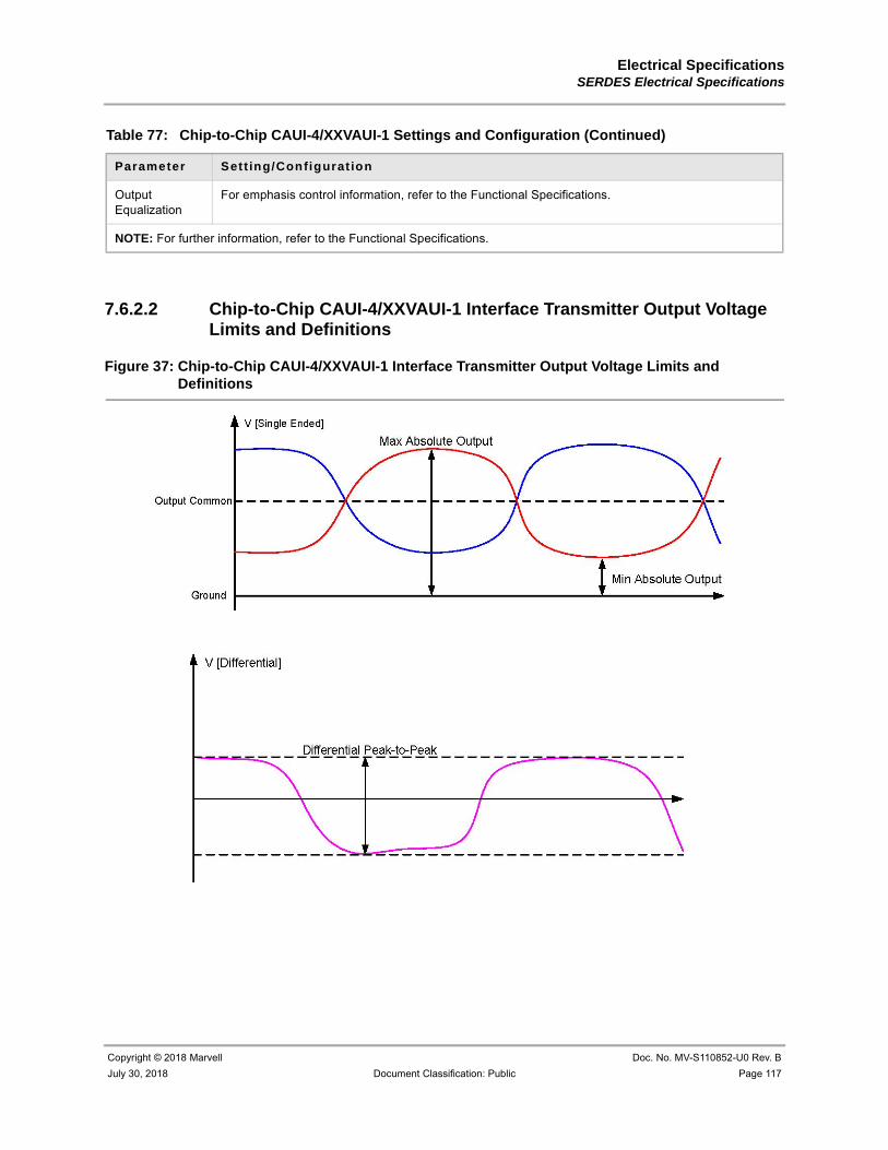
Electrical SpecificationsSERDES Electrical Specifications
Copyright © 2018 Marvell Doc. No. MV-S110852-U0 Rev. B
July 30, 2018 Document Classification: Public Page 117
7.6.2.2 Chip-to-Chip CAUI-4/XXVAUI-1 Interface Transmitter Output Voltage Limits and Definitions
Figure 37: Chip-to-Chip CAUI-4/XXVAUI-1 Interface Transmitter Output Voltage Limits and Definitions
Output Equalization
For emphasis control information, refer to the Functional Specifications.
NOTE: For further information, refer to the Functional Specifications.
Table 77: Chip-to-Chip CAUI-4/XXVAUI-1 Settings and Configuration (Continued)
Parameter Sett ing/Configurat ion

88X5113 Datasheet - Public
Doc. No. MV-S110852-U0 Rev. B Copyright © 2018 Marvell
Page 118 Document Classification: Public July 30, 2018
Figure 38: Chip-to-Chip CAUI-4/XXVAUI-1 Transmitter Output Differential Amplitude and Eye Opening

Electrical SpecificationsSERDES Electrical Specifications
Copyright © 2018 Marvell Doc. No. MV-S110852-U0 Rev. B
July 30, 2018 Document Classification: Public Page 119
7.6.3 100GBASE-CR4/50GBASE-CR2/25GBASE-CR Electrical Characteristics
7.6.3.1 100GBASE-CR4/50GBASE-CR2/25GBASE-CR Interface Transmitter and Receiver Characteristics
Table 78: 100GBASE-CR4/50GBASE-CR2/25GBASE-CR Interface Transmitter and Receiver Characteristics
Symbol Parameter Min Max Units Notes
BR Baud rate 25.78125 Gbps –
Bppm Baud rate tolerance -100 100 ppm 1
UI Unit interval 38.787879 ps –
Transmitter Parameters
Vodis Transmitter disabled output differential noise level – 35 mV –
Vodpp Output differential maximum peak-to-peak – 1200 mV –
Vf Output waveform - Steady-state voltage 0.34 0.6 V 12
Vlfpp Output waveform -Linear fit pulse peak 0.45*Vf – V 12
Ncs Output waveform - Normalized coefficient step size 0.0083 0.05 – 13
Prec Output waveform - Pre-cursor full-scale range 1.54 – – 14
Pstc Output waveform - Post-cursor full-scale range 4 – – 14
Vsnr Transmitter signal-to-noise-and-distortion ratio 26 – dB 15
Vosdc DC Common-mode voltage limits 0.0 1.9 V –
Vosac AC Common-mode voltage limits (RMS) – 30 mV –
RLOD Return loss differential output See note #2. dB 2, 5
RLOCD Return loss Common-Mode to Differential output See note #3. dB 3, 5
RLOC Return loss Common-Mode output 2 – dB 5, 16
Juctx Output jitter -Effective bounded uncorrelated, peak-to-peak
– 0.1 UI 17
Jeotx Output Even-Odd jitter – 0.035 UI 11
Jtpptx Output jitter - Effective total uncorrelated, peak-to-peak – 0.18 UI 6, 9, 17
Receiver Parameters
Vidpp Input differential voltage – 1200 mV 8
RLID Return loss differential input See note #2. dB 2, 5
RLIDC Differential to common mode input return loss See note #4. dB 4, 5
88X5113 Datasheet - Public
Doc. No. MV-S110852-U0 Rev. B Copyright © 2018 Marvell
Page 120 Document Classification: Public July 30, 2018
Rit Receiver interference tolerance See note #7. UI 7
Rjt Receiver jitter tolerance See note #10. UI 6, 10
Table 78: 100GBASE-CR4/50GBASE-CR2/25GBASE-CR Interface Transmitter and Receiver Characteristics (Continued)
Symbol Parameter Min Max Units Notes
Note
The load is 100Ω differential for these parameters, unless otherwise specified. General Comment: The Tx table is defined on TP2 as defined in 92.11 Test fixtures in 802.3 IEEE standard. General Comment: The Rx table is defined onTP3 as defined in 92.11 Test fixtures in 802.3 IEEE standard. • Defines the allowable reference clock difference and Rx baud rate tolerance relative
to nominal. Tx baud rate is derived from multiplication of the reference clock (0 ppm delta).
• RLOD and RLID are defined accordingly: For 10 MHz -8 GHz RLOD/RLID>9.5-0.37*f [dB] (Frequency defined in GHz). For 8 GHz -19 GHz RLOD/RLID>4.75-7.4*Log(f/14) [dB] (Frequency defined in GHz).
• RLOCD and RLID Care defined accordingly: For 10 MHz -12.89 GHz RLOCD/RLIDC>22-(20/25.78)*f [dB] (Frequency defined in GHz). For 12.89 GHz -19 GHz RLOCD/RLIDC>15-(6/25.78)*f [dB] (Frequency defined in GHz).
• Relative to 100Ω differential and 25Ω common mode.
• Defined with a Bit Error Rate (BER) of 10^-5.
• Defined according to IEEE 802.3 section 92.8.4.4 Receiver interference tolerance test.
• Vidpp refers to the peak-to-peak. Defined according to IEEE 802.3 section 92.8.4.1 Receiver input amplitude tolerance.
• The output Tx jitter is defined when applying the effect of a single-pole high-pass fil-ter on the jitter. The high-pass filter 3 dB point is located at 10 MHz.
• Defined according to IEEE802.3 section 92.8.4.5 Receiver jitter tolerance.
• Defined for a PRBS9 pattern according to section 92.8.3.8.1 Even-odd jitter in 802.3 IEEE standard.
• The transmitter output waveform follows IEEE requirements as specified in section 92.8.3.5.2 Steady-state voltage and linear fit pulse peak.
• The transmitter output waveform follows IEEE requirements as specified in section 92.8.3.5.4 Coefficient step size.
• The transmitter output waveform follows IEEE requirements as specified in section 92.8.3.5.5 Coefficient range.
• The transmitter output waveform follows IEEE requirements as specified in section 92.8.3.7 Transmitter output noise and distortion.
• Defined from 200 MHz to 19 GHz.
• The transmitter jitter follows IEEE requirements as specified in section 92.8.3.8.2 Effective bounded uncorrelated jitter and effective random jitter.

Electrical SpecificationsSERDES Electrical Specifications
Copyright © 2018 Marvell Doc. No. MV-S110852-U0 Rev. B
July 30, 2018 Document Classification: Public Page 121
Table 79: 100GBASE-CR4/50GBASE-CR2/25GBASE-CR Settings and Configuration
Parameter Sett ing/Configurat ion
Vods The Vods is the output differential amplitude configurable range.When driving a test load, the minimum value is achieved with AMP=TBD and PRE=TBD, and the maximum value is achieved with AMP=TBD and PRE=TBD. Output amplitude and pre-emphasis are configurable.
Viddp The Viddp is the input differential voltage.The maximum single-ended voltage (common mode voltage and swing voltage) must not exceed 1.8V.
Vodpp To achieve the specifications at Tp1a, the use of emphasis may be needed.
Output Equalization
For emphasis control information, refer to the Functional Specifications.
NOTE: For further information, refer to the Functional Specifications.

88X5113 Datasheet - Public
Doc. No. MV-S110852-U0 Rev. B Copyright © 2018 Marvell
Page 122 Document Classification: Public July 30, 2018
7.6.3.2 100GBASE-CR4/50GBASE-CR2/25GBASE-CR Interface Transmitter Output Voltage Limits and Definitions
Figure 39: 100GBASE-CR4/50GBASE-CR2/25GBASE-CR Interface Transmitter Output Voltage Limits and Definitions

Electrical SpecificationsSERDES Electrical Specifications
Copyright © 2018 Marvell Doc. No. MV-S110852-U0 Rev. B
July 30, 2018 Document Classification: Public Page 123
7.6.4 100GBASE-KR4/50GBASE-KR2/25GBASE-KR Electrical Characteristics
7.6.4.1 100GBASE-KR4/50GBASE-KR2/25GBASE-KR Interface Transmitter and Receiver Characteristics
Table 80: 100GBASE-KR4/50GBASE-KR2/25GBASE-KR Interface Transmitter and Receiver Characteristics
Symbol Parameter Min Max Units Notes
BR Baud rate 25.78125 Gbps –
Bppm Baud rate tolerance -100 100 ppm 1
UI Unit interval 38.787879 ps –
Transmitter Parameters
Vodis Transmitter disabled output differential noise level – 30 mV –
Vodpp Output differential maximum peak-to-peak – 1200 mV –
Vf Output waveform - Steady-state voltage 0.4 0.6 V 12
Vlfpp Output waveform -Linear fit pulse peak 0.71*Vf – V 12
Ncs Output waveform - Normalized coefficient step size 0.0083 0.05 – 13
Prec Output waveform - Pre-cursor full-scale range 1.54 – – 14
Pstc Output waveform - Post-cursor full-scale range 4 – – 14
Vsnr Transmitter signal-to-noise-and-distortion ratio 27 – dB 15
Vosdc DC Common-mode voltage limits 0.0 1.9 V –
Vosac AC Common-mode voltage limits (RMS) – 12 mV –
RLOD Return loss differential output See note #2. dB 2, 5
RLOC Return loss Common-Mode output See note #3. dB 5, 16
Juctx Output jitter - Effective bounded uncorrelated, peak-to-peak – 0.1 UI 17
Jeotx Output Even-Odd jitter – 0.035 UI 11
Jtpptx Output jitter - Effective total uncorrelated, peak-to-peak – 0.18 UI 6, 9, 17
Receiver Parameters
Vidpp Input differential voltage – 1200 mV 8
RLID Return loss differential input See note #2. dB 2, 5
RLIDC Differential to common mode input return loss See note #4. dB 4, 5

88X5113 Datasheet - Public
Doc. No. MV-S110852-U0 Rev. B Copyright © 2018 Marvell
Page 124 Document Classification: Public July 30, 2018
Rit Receiver interference tolerance See note #7. UI 7
Rjt Receiver jitter tolerance See note #10. UI 6, 10
Table 80: 100GBASE-KR4/50GBASE-KR2/25GBASE-KR Interface Transmitter and Receiver Characteristics (Continued)
Symbol Parameter Min Max Units Notes
Note
The load is 100Ω differential for these parameters, unless otherwise specified. General Comment: The Tx table is defined on TP0a as defined in 93.8.1.1 Transmitter test fixture in the IEEE 802.3 standard. General Comment: The Rx table is defined on TP5a as defined in 93.8.2.1 Receiver test Micmac in the IEEE 802.3 standard. • Defines the allowable reference clock difference and Rx baud rate tolerance relative
to nominal. Tx baud rate is derived from multiplication of the reference clock (0 ppm delta).
• RLOD and RLID are defined accordingly: For 50 MHz -6 GHz RLOD/RLID>12.05-f [Frequency] (Frequency defined in GHz). For 6 GHz -19 GHz RLOD/RLID>6.5-0.075*f [dB] (Frequency defined in GHz).
• RLOC is defined accordingly: For 50 MHz -6 GHz RLOC>9.05-f [dB] (Frequency defined in GHz). For 6 GHz -19 GHz RLOC>3.5-0.075*f [dB] (Frequency defined in GHz).
• RLIDC is defined accordingly: For 50 MHz -6.95 GHz RLIDC>25-1.44*f [dB] (Fre-quency defined in GHz). For 6.95 GHz -19 GHz RLIDC>15 [dB].
• Relative to 100Ω differential and 25Ω common mode.
• Defined with a Bit Error Rate (BER) of 10^-5.
• Defined according to IEEE 802.3 section 93.8.2.3 Receiver interference tolerance.
• Vidpp refers to the peak-to-peak.
• The output Tx jitter is defined when applying the effect of a single-pole high-pass fil-ter on the jitter. The high-pass filter 3 dB point is located at 10 MHz.
• Defined according to IEEE 802.3 section 93.8.2.4 Receiver jitter tolerance
• Defined for a PRBS9 pattern according to section 92.8.3.8.1 Even-odd jitter in the IEEE 802.3 standard.
• The transmitter output waveform follows IEEE requirements as specified in section 93.8.1.5.2 Steady-state voltage and linear fit pulse peak.
• The transmitter output waveform follows IEEE requirements as specified in section 93.8.1.5.4 Coefficient step size.
• The transmitter output waveform follows IEEE requirements as specified in section 93.8.1.5.5 Coefficient range.
• The transmitter output waveform follows IEEE requirements as specified in section 93.8.1.6 Transmitter output noise and distortion.
• The transmitter output jitter follows IEEE requirements as specified.

Electrical SpecificationsSERDES Electrical Specifications
Copyright © 2018 Marvell Doc. No. MV-S110852-U0 Rev. B
July 30, 2018 Document Classification: Public Page 125
Table 81: 100GBASE-KR4/50GBASE-KR2/25GBASE-KR Settings and Configuration
Parameter Sett ing/Configurat ion
Vods The Vods is the output differential amplitude configurable range.When driving a test load, the minimum value is achieved with AMP=TBD and PRE=TBD, and the maximum value is achieved with AMP=TBD and PRE=TBD. Output amplitude and pre-emphasis are configurable.
Viddp The Viddp is the input differential voltage.The maximum single-ended voltage (common mode voltage and swing voltage) must not exceed 1.8V.
Vodpp To achieve the specifications at Tp1a, the use of emphasis may be needed.
Output Equalization
For emphasis control information, refer to the Functional Specifications.
NOTE: For further information, refer to the Functional Specifications.

88X5113 Datasheet - Public
Doc. No. MV-S110852-U0 Rev. B Copyright © 2018 Marvell
Page 126 Document Classification: Public July 30, 2018
7.6.4.2 100GBASE-KR4/50GBASE-KR2/25GBASE-KR Interface Transmitter Output Voltage Limits and Definitions
Figure 40: 100GBASE-KR4/50GBASE-KR2/25GBASE-KR Interface Transmitter Output Voltage Limits and Definitions

Electrical SpecificationsSERDES Electrical Specifications
Copyright © 2018 Marvell Doc. No. MV-S110852-U0 Rev. B
July 30, 2018 Document Classification: Public Page 127
7.6.5 40 Gbps Parallel Physical Interface (XLPPI) Electrical Characteristics
7.6.5.1 40 Gbps Parallel Physical Interface (XLPPI) Interface Transmitter and Receiver Characteristics
Table 82: XLPPI Interface Transmitter and Receiver Characteristics
Symbol Parameter Min Max Units Notes
BR Baud rate 10.3125 Gbps –
Bppm Baud rate tolerance -100 100 ppm 1
UI Unit interval 96.969697 ps –
Transmitter Parameters
Vodpp Output differential maximum peak-to-peak 190 700 mV –
Vos Single-ended output voltage -0.3 1.9 V 11
QSQ Signal-to-noise-ratio 45 – V/V 14
Tr/Tf Output differential transition time 28 – ps 2, 11
RLOD Return loss differential output See note #3. 3, 4,11
RLOC Return loss common mode output See note #3. 3, 4, 11
Tlskew Output lane-to-lane skew – 29 ns –
Tlskew v Output lane-to-lane skew variation – 200 ps –
dZM Termination mismatch – 5 % 9, 11
Vocmac Output AC common mode voltage, RMS – 15 mV 11, 12
Jddpw st Output jitter - Data dependent pulse width shrinkage – 0.07 UI 11
J2tx Output 99% jitter - J2, peak-to-peak – 0.17 UI 8, 11
J9tx Output jitter - J9, peak-to-peak – 0.29 UI 8, 11
Jtpptx Output jitter - Total, peak-to-peak – 0.22 UI 5, 8, 11
Receiver Parameters
Vidpps Input differential sensitivity 300 – mV 5,7,11
Vidpp Input differential voltage - 850 mV 5, 7. 11 – 850 mV 5,7,11
RLID Return loss differential input See note # 3. dB 3, 4, 11
RLICD Reflected input common mode to differential conversion 10 – dB 10, 11
Rlskew Input lane-to-lane skew – 160 ns –

88X5113 Datasheet - Public
Doc. No. MV-S110852-U0 Rev. B Copyright © 2018 Marvell
Page 128 Document Classification: Public July 30, 2018
Rlskew v Input lane-to-lane skew variation – 4 ns –
J2rx Input 99% jitter - J2, peak-to-peak – 0.42 UI 6, 11
J9rx Input jitter - J9, peak-to-peak – 0.65 UI 11
Jddpw sr Input jitter - Data dependent pulse width shrinkage – 0.34 UI 11, 13
Vicmac Input AC common mode voltage, RMS – 7.5 mV 11, 12
Table 82: XLPPI Interface Transmitter and Receiver Characteristics (Continued)
Symbol Parameter Min Max Units Notes
Note
The load is 100Ω differential for these parameters, unless otherwise specified. The reference points are according to Figure 86-2 in the IEEE Std 802.3-2010. • Defines the allowable reference clock difference and Rx baud rate tolerance relative
to nominal. Tx baud rate is derived from multiplication of the reference clock (zero ppm delta).
• Defined from 20 to 80% of the signal's voltage levels when driving a pattern consist-ing of eight consecutive ones followed by an equal run of zeros with no equalization. Maximum transition time is limited by mask as defined in IEEE 802.3 section 86A.5.3.6 Eye mask for TP1a and TP4.
• RLOD/RLID are defined from:
• 10.0 MHz to 4.11 GHz RLOD/RLID>12-2(Frequency)^0.5 [dB] (Frequency defined in GHz). For 4.11 GHz to 11.1 GHz RLOD/RLID>6.3-13log(Frequency/5.5)[dB] (Fre-quency defined in GHz). RLOC is defined from:
• 10.0 MHz to 2.5 GHz RLOC>7-1.6*(Frequency) [dB] (Frequency defined in GHz). For 2.5 GHz to 11.1 GHz RLOC>3dB.
• Relative to 100Ω differential and 25Ω common mode. Return loss includes contribu-tions from on-chip circuitry, chip packaging, and off-chip optimized components related to the transmitter/receiver breakout.
• Defined with a Hit Ratio of 5*10^-5.
• Defined with all but 1 percent of occurrences.
• Vidpps refers to the internal eye opening while Vidp prefers to the peak-to-peak.
• The output Tx jitter is defined when applying the effect of a single-pole high-pass fil-ter on the-jitter. The high-pass filter 3 dB point is located at 4 MHz.
• Defined at 1 MHz frequency. Defined according to section 86A.5.3.2 Termination mismatch in the IEEE Std 802.3-2010.
• Defined from 10 MHz to 11.1 GHz.
• Defined at reference points TP1A or TP4A. For maximal allowed interconnect char-acteristics between points TP0 and TP1A or pointsTP4A and TP5, refer to Section 86A.5.1.1.1 Reference insertion losses of HC Band MCB in IEEE Std 803.2-2010.
• The parameter at any time is the average of signal(+) and signal(-) at that time. This parameter is calculated by applying the histogram function over 1 UI to the common mode signal.
• Defined in coherence with Section 86A.5.3.4 Data Dependent Pulse Width Shrink-age in IEEE Std 803.2-2010.
• The Qdq ratio is defined under the restrictions of the eye mask as defined in IEEE 802.3 section 86A.5.3.6 Eye mask for TP1a and TP4.

Electrical SpecificationsSERDES Electrical Specifications
Copyright © 2018 Marvell Doc. No. MV-S110852-U0 Rev. B
July 30, 2018 Document Classification: Public Page 129
7.6.5.2 XLPPI Interface Transmitter Output Voltage Limits and Definitions
Figure 41: XLPPI Interface Transmitter Output Voltage Limits and Definitions
Table 83: XLPPI Settings and Configuration
Parameter Sett ing/Configurat ion
Vods The Vods is the output differential amplitude configurable range.When driving a test load, the minimum value is achieved with AMP=TBD and PRE=TBD, and the maximum value is achieved with AMP=TBD and PRE=TBD. Output amplitude and pre-emphasis are configurable.
Viddp The Viddp is the input differential voltage.The maximum single-ended voltage (common mode voltage and swing voltage) must not exceed 1.8V.
Vodpp To achieve the specifications at P1a, the use of emphasis may be needed.
Output Equalization
Tx emphasis may be configured to achieve the required deterministic jitter at the module connector. For emphasis control information, refer to the Functional Specifications.
NOTE: For further information, refer to the Functional Specifications.

88X5113 Datasheet - Public
Doc. No. MV-S110852-U0 Rev. B Copyright © 2018 Marvell
Page 130 Document Classification: Public July 30, 2018
Figure 42: XLPPI Transmitter Output Differential Amplitude and Eye Opening

Electrical SpecificationsSERDES Electrical Specifications
Copyright © 2018 Marvell Doc. No. MV-S110852-U0 Rev. B
July 30, 2018 Document Classification: Public Page 131
7.6.6 40 Gbps Attachment Unit Interface (XLAUI) Electrical Characteristics
7.6.6.1 40 Gbps Attachment Unit Interface (XLAUI) Interface Transmitter and Receiver Characteristics
Table 84: XLAUI Interface Transmitter and Receiver Characteristics
Symbol Parameter Min Max Units Notes
BR Baud rate 10.3125 Gbps –
Bppm Baud rate tolerance -100 100 ppm 1
UI Unit interval 96.969697 ps –
Transmitter parameters
Vodpp Output differential peak-to-peak 400 760 mV 9
Vos Single-ended output voltage -0.4 1.9 V –
DEtx Output de-emphasis 4.4 7 dB –
Tr/Tf Output differential transition time 24 – ps 2
RLOD Return loss differential output 12 – dB 3,4
RLOC Return loss common mode output 9 – dB 3,4
Tlskew Output lane-to-lane skew – 28 ns –
Tlskew v Output lane-to-lane skew variation – 200 ps –
dZM Termination mismatch – 5 % 10
Vocmac Output AC common mode voltage – 15 mVRMS -
Jdtx Output jitter - Deterministic, peak-to-peak – 0.17 UI -
Jtpptx Output jitter - Total, peak-to-peak – 0.32 UI 5, 8
Evodpp Output eye width at Vodpp (min) 0.24 – UI –
Receiver parameters
Vidpps Input differential sensitivity 85 – mV 7
Vidpp Input differential voltage – 850 mV 7
RLID Return loss differential input 12 – dB 3, 4
RLICD Return loss common to differential input 15 – dB 11
Rlskew Input lane-to-lane skew – 161 ns –
Rlskew v Input lane-to-lane skew variation – 3.8 ns –
Jtrlsx Input jitter - Sinusoidal, low frequency – 5 UI 12

88X5113 Datasheet - Public
Doc. No. MV-S110852-U0 Rev. B Copyright © 2018 Marvell
Page 132 Document Classification: Public July 30, 2018
Jtrsx Input jitter - Sinusoidal, high frequency – 0.05 UI 13
Jdrx Input jitter - Deterministic, peak-to-peak – 0.42 UI –
Jtpprx Input jitter - Total, peak-to-peak – 0.62 UI 5, 6
Vicmac Input AC common mode voltage – 20 mVRMS –
Table 84: XLAUI Interface Transmitter and Receiver Characteristics (Continued)
Symbol Parameter Min Max Units Notes
Note
The load is 100Ω differential for these parameters, unless otherwise specified. • Defines the allowable reference clock difference and Rx baud rate tolerance relative
to nominal. Tx baud rate is derived from multiplication of the reference clock (0 ppm delta).
• Defined from 20 to 80% of the signal's voltage levels when driving a pattern consist-ing of eight consecutive ones followed by an equal run of zeros with no equalization. Max transition time is limited by mask as defined in IEEE 802.3 section 83A.3.3.5 Transmitter eye mask and transmitter jitter definition.
• Defined from 10 MHz to 2.125 GHz. For 2.125 GHz -11.1 GHz RLOD/RLID>6.5-13.33log(Frequency/5.5)[dB] (Frequency defined in GHz). For 2.125 GHz -7.1 GHz RLOC>3.5-13.33log(Frequency/5.5)[dB] (Frequency defined in GHz). For 7.1 GHz -11.1 GHz RLOC>2[dB].
• Relative to 100Ω differential and 25Ω common mode. Return loss includes contribu-tions from on-chip circuitry, chip packaging, and off-chip optimized components related to the transmitter/receiver breakout.
• Defined with a Bit Error Rate (BER) of 10^-12.
• This parameter does not include sinusoidal components.
• Vidpps refers to the internal eye opening while Vidpp refers to the peak-to-peak.
• The output Tx jitter is defined when applying the effect of a single-pole high-pass fil-ter on the jitter. The high-pass filter 3 dB point is located at 4 MHz.
• Defined with emphasis disabled.
• Defined at 1 MHz frequency. Defined according to section 86A.5.3.2 Termination mismatch in IEEE Std 802.3ba.
• Defined from 10 MHz to 11.1 GHz.
• Defined below 40 kHz.
• Defined from 4 MHz to 20 MHz.

Electrical SpecificationsSERDES Electrical Specifications
Copyright © 2018 Marvell Doc. No. MV-S110852-U0 Rev. B
July 30, 2018 Document Classification: Public Page 133
Table 85: XLAUI Settings and Configuration
Parameter Sett ing/Configurat ion
Vods The Vods is the output differential amplitude configurable range.When driving a test load, the minimum value is achieved with AMP=TBD and PRE=TBD, and the maximum value is achieved with AMP=TBD and PRE=TBD. Output amplitude and pre-emphasis are configurable.
Viddp The Viddp is the input differential voltage.The maximum single-ended voltage (common mode voltage and swing voltage) must not exceed 1.8V.
Output Equalization
Tx emphasis may be configured to achieve the required deterministic jitter at the module connector. For emphasis control information, refer to the Functional Specifications.
NOTE: For further information, refer to the Functional Specifications.

88X5113 Datasheet - Public
Doc. No. MV-S110852-U0 Rev. B Copyright © 2018 Marvell
Page 134 Document Classification: Public July 30, 2018
7.6.6.2 XLAUI Interface Transmitter Output Voltage Limits and Definitions
Figure 43: XLAUI Interface Transmitter Output Voltage Limits and Definitions
Figure 44: XLAUI Transmitter Output Differential Amplitude and Eye Opening

Electrical SpecificationsSERDES Electrical Specifications
Copyright © 2018 Marvell Doc. No. MV-S110852-U0 Rev. B
July 30, 2018 Document Classification: Public Page 135
7.6.7 40GBASE-CR4 Electrical Characteristics
7.6.7.1 40GBASE-CR4 Interface Transmitter and Receiver Characteristics
Table 86: 40GBASE-CR4 Interface Transmitter and Receiver Characteristics
Symbol Parameter Min Max Units Notes
BR Baud rate 10.3125 Gbps –
Bppm Baud rate tolerance -100 100 ppm 1
UI Unit interval 96.969697 ps –
Transmitter Parameters
Vodis Transmitter disabled output differential noise level – 30 mV –
Vodpp Output differential maximum peak-to-peak – 1200 mV –
DEtx Output de-emphasis See note 12. – 12
Vos Common-mode voltage limits 0.0 1.9 V –
RLOD Return loss differential output 10 – dB 2, 3
Tlskew Output lane-to-lane skew – 54 ns –
Tlskew v Output lane-to-lane skew variation – 600 ps –
Jdtx Output jitter - Deterministic, peak-to-peak – 0.15 UI –
Jdcdtx Output duty cycle distortion – 0.035 UI 9, 10
Jrndtx Output jitter - Random – 0.15 UI 4
Jtpptx Output jitter - Total, peak-to-peak – 0.28 UI 4, 7, 11
Receiver Parameters
Vidpp Input differential voltage – 1200 mV 6
RLID Return loss differential input 10 – dB 2, 3
RLIDC Differential to common mode input return loss 10 – dB 13
Rlskew Input lane-to-lane skew – 134 ns –
Rlskew v Input lane-to-lane skew variation – 3.4 ns –
Js Input sinusoidal jitter – 0.115 UI 5
Jrndrx Input random jitter – 0.13 UI 4, 5
Jdcd Input duty cycle distortion – 0.035 UI 5
Vinamp Calibrated far-end crosstalk – 6.3 mVRMS 5, 8
ICN Calibrated integrated crosstalk noise – 3.7 mVRMS 5

88X5113 Datasheet - Public
Doc. No. MV-S110852-U0 Rev. B Copyright © 2018 Marvell
Page 136 Document Classification: Public July 30, 2018
Note
The load is 100Ω differential for these parameters, unless otherwise specified.
Defines the allow able reference clock difference and Rx baud rate tolerance relative to nominal. Tx baud rate is derived from multiplication of the reference clock (zero ppm delta).
Defined from 50 MHz to 2.5 GHz.
For 2.5 GHz -7.5 GHz RLOD>9-12log(Frequency/2.5)[dB] (Frequency defined in GHz).
For 2.5 GHz -7.5 GHz RLID>9-12log(Frequency/2.5)[dB] (Frequency defined in GHz).
Relative to 100Ω differential and 25Ω common mode. Return loss includes contributions from on-chip circuitry, chip packaging, and off-chip optimized components related to the transmitter/receiver breakout.
Defined with a Bit Error Rate (BER) of 10^-12.
Defined for interference tests according IEEE 802.3 section 85.8.4.2 Receiver interference tolerance test.
Vidpp refers to the peak-to-peak.
The output Tx jitter is defined w hen applying the effect of a single-pole high-pass filter on the jitter. The high-pass filter 3 dB point is located at 4 MHz.
The receiver tolerates noise at an amplitude specified under receiver interference tolerance test1.
The value for test2 is 2.2 mV.
Jdcdtx is included as a part of Jdtx.
Defined for a 1010 pattern and includes the entire range of emphasis.
The jitter is defined with emphasis off.
The transmitter output waveform follow s IEEE requirements as specified in section 85.8.3.3 Transmitter output waveform.
Defined from 10 MHz to 10 GHz.
Table 87: 40GBASE-CR4 Settings and Configuration
Parameter Sett ing/Configurat ion
Viddp The Viddp is the input differential voltage.The maximum single-ended voltage (common mode voltage and swing voltage) must not exceed 1.8V.
Output Equalization
The default as determined by the IEEE is 3 TAP FIR optimized per interconnect.
NOTE: For further information, refer to the Functional Specifications.

Electrical SpecificationsSERDES Electrical Specifications
Copyright © 2018 Marvell Doc. No. MV-S110852-U0 Rev. B
July 30, 2018 Document Classification: Public Page 137
7.6.7.2 40GBASE-CR4 Interface Transmitter Output Voltage Limits and Definitions
Figure 45: 40GBASE-CR4Interface Transmitter Output Voltage Limits and Definitions
Figure 46: 40GBASE-CR4Transmitter Output Differential Amplitude and Eye Opening

88X5113 Datasheet - Public
Doc. No. MV-S110852-U0 Rev. B Copyright © 2018 Marvell
Page 138 Document Classification: Public July 30, 2018
7.6.8 40GBASE-KR4 Electrical Characteristics
7.6.8.1 40GBASE-KR4 Interface Transmitter and Receiver Characteristics
Table 88: 40GBASE-KR4 Interface Transmitter and Receiver Characteristics
Symbol Parameter Min Max Units Notes
BR Baud rate 10.3125 Gbps –
Bppm Baud rate tolerance -100 100 ppm 1
UI Unit interval 96.969697 ps –
Transmitter Parameters
Vodis Transmitter disabled output differential noise level – 30 mV –
Vodpp Output differential maximum peak-to-peak – 1200 mV –
Vos Common-mode voltage limits 0 1.9 V –
Tr/Tf Output differential transition time 24 47 ps 10
RLOD Return loss differential output 9 – dB 2, 3
RLOC Return loss common mode output 6 – dB 2, 3
Tlskew Output lane-to-lane skew – 557 UI –
Tlskew v Output lane-to-lane skew variation – 6 UI –
Jdtx Output jitter - Deterministic, peak-to-peak – 0.15 UI –
Jdcdtx Output duty cycle distortion – 0.035 UI 10, 11
Jrndtx Output jitter - Random – 0.15 UI 4
Jtpptx Output jitter - Total, peak-to-peak – 0.28 UI 4, 7
Receiver Parameters
Vidpp Input differential voltage – 1200 mV 6
RLID Return loss differential input 9 – dB 2, 3
Rlskew Input lane-to-lane skew – 1382 UI –
Rlskew v Input lane-to-lane skew variation – 35 UI –
Js Input sinusoidal jitter – 0.115 UI 5
Jrndrx Input random jitter – 0.13 UI 4, 5
Jdcd Input duty cycle distortion – 0.035 UI 5
Vinamp Input broadband noise amplitude – 5.2 mVRMS 5, 9

Electrical SpecificationsSERDES Electrical Specifications
Copyright © 2018 Marvell Doc. No. MV-S110852-U0 Rev. B
July 30, 2018 Document Classification: Public Page 139
mTC Test Channel Magnitude factor 1 – 5, 8
Table 88: 40GBASE-KR4 Interface Transmitter and Receiver Characteristics (Continued)
Symbol Parameter Min Max Units Notes
Note
The load is 100Ω differential for these parameters, unless otherwise specified.
Defines the allow able reference clock difference and Rx baud rate tolerance relative to nominal.
Tx baud rate is derived from multiplication of the reference clock (0 ppm delta).
Defined from 50 MHz to 2.5 GHz.
For 2.5 GHz -7.5 GHz RLOD>9-12log(Frequency/2.5)[dB] (Frequency defined in GHz).
For 2.5 GHz -7.5 GHz RLOC>6-12log(Frequency/2.5)[dB] (Frequency defined in GHz).
For 2.5 GHz -7.5 GHz RLID>9-12log(Frequency/2.5)[dB] (Frequency defined in GHz).
Relative to 100Ω differential and 25Ω common mode. Return loss includes contributions from on-chip circuitry, chip packaging, and off-chip optimized components related to the transmitter/receiver breakout.
Defined with a Bit Error Rate (BER) of 10^-12.
Defined for interference tests according IEEE 802.3 Annex 69A.
For informative interconnect characteristics, refer to IEEE 802.3 Annex 69B.
Vidpp refers to the peak-to-peak.
The output Tx jitter is defined w hen applying the effect of a single-pole high-pass filter on the jitter.
The high-pass filter 3 dB point is located at 4 MHz.
mTC describes the insertion loss transmission magnitude relative to the maximal allowed fitted attenuation mask Amax over a predefined frequency range.
Defined for test1. The value for test2 is 0.5.
The receiver tolerates noise at an amplitude specified under receiver interference tolerance test1. The value for test2 is 12 mV.
Jdcdtx is included as a part of Jdtx.
Defined for a 1010 pattern and includes the entire range of emphasis.
The transmitter output waveform follow s IEEE requirements as specified in section 72.7.1.10 Transmitter output waveform requirements.
Table 89: 40GBASE-KR4 Settings and Configuration
Parameter Setting/Configurat ion
Viddp The Viddp is the input differential voltage.The maximum single-ended voltage (common mode voltage and swing voltage) must not exceed 1.8V.

88X5113 Datasheet - Public
Doc. No. MV-S110852-U0 Rev. B Copyright © 2018 Marvell
Page 140 Document Classification: Public July 30, 2018
7.6.8.2 40GBASE-KR4 Interface Transmitter Output Voltage Limits and Definitions
Figure 47: 40GBASE-KR4 Interface Transmitter Output Voltage Limits and Definitions
Output Equalization
The default as determined by the IEEE is 3 TAP FIR optimized per interconnect.
NOTE: For further information, refer to the Functional Specifications.
Table 89: 40GBASE-KR4 Settings and Configuration (Continued)
Parameter Setting/Configurat ion

Electrical SpecificationsSERDES Electrical Specifications
Copyright © 2018 Marvell Doc. No. MV-S110852-U0 Rev. B
July 30, 2018 Document Classification: Public Page 141
Figure 48: 40GBASE-KR4 Transmitter Output Differential Amplitude and Eye Opening

88X5113 Datasheet - Public
Doc. No. MV-S110852-U0 Rev. B Copyright © 2018 Marvell
Page 142 Document Classification: Public July 30, 2018
7.6.9 SFP+ Interface (SFI) Limiting Module Electrical Characteristics
7.6.9.1 SFI Transmitter and Receiver Characteristics
Table 90: SFI Transmitter and Receiver Characteristics
Symbol Parameter Min Max Units Notes
BR Baud rate 10.3125 Gbps –
Bppm Baud rate tolerance -100 100 ppm 1
UI Unit interval 96.969697 ps –
Transmitter parameters
Vodpp Output differential peak-to-peak 190 700 mV 9,14,7
Vos Single-ended output voltage -0.3 1.9 V 13
DEtx Output de-emphasis 4.4 7 dB 13
Tr/Tf Output differential transition time 24 – ps 2, 13
RLOD Return loss differential output 12 – dB 3,4,13
RLOC Return loss common mode output 9 – dB 3,4,13
dZM Termination mismatch – 5 % 10,13
Vocmac Output AC common mode voltage – 12 mVRMS 13,15
Jutx Output jitter - Uncorrelated, RMS – 0.023 UI 5,14,12
Jddpw st Output jitter - Data dependent pulse width shrinkage – 0.055 UI 14
Jddtx Output jitter - Data dependent, peak-to-peak – 0.1 UI 14
Jtpptx Output jitter - Total, peak-to-peak – 0.28 UI 8,14,17
Receiver parameters
Vidpps Input differential sensitivity 300 – mV 7,14
Vidpp Input differential voltage – 850 mV 7,14
RLID Return loss differential input 12 – dB 3,4,13
RLICD Reflected input common mode to differential conversion
15 – -dB 11,13
J2 Input 99% jitter - peak-to-peak – 0.42 UI 6,14,16
Jddpw sr Input jitter - Data dependent pulse width shrinkage – 0.3 UI 14, 16
Jtpprx Input jitter - Total, peak-to-peak – 0.7 UI 5,14,16
Vicmac Input AC common mode voltage, RMS – 7.5 mVRMS 14,15,16
Electrical SpecificationsSERDES Electrical Specifications
Copyright © 2018 Marvell Doc. No. MV-S110852-U0 Rev. B
July 30, 2018 Document Classification: Public Page 143
Note
The load is 100Ω differential for these parameters, unless otherwise specified.
The reference points are according to Table 10 SFI Reference Points in SFF 8431 Rev. 4.1 standard.
Defines the allow able reference clock difference and Rx baud rate tolerance relative to nominal. Tx baud rate is derived from multiplication of the reference clock (zero ppm delta).
Defined from 20 to 80% of the signal's voltage levels w hen driving a pattern consisting of 8 consecutive ones follow ed by an equal run of zeros with no equalization. Max transition time is limited by mask as defined in SFF 8431 Rev. 4.1 standard. Figure 19 Transmitter Differential Output Compliance Mask at B and B.
RLOD/RLID are defined from 10 MHz to 2.8 GHz.
Relative to 100Ω differential and 25Ω common mode. Return loss includes contributions from on-chip circuitry, chip packaging, and off-chip optimized components related to the transmitter/receiver breakout.
Defined with a Bit Error Rate (BER) of 10^-12.
Defines with all but 1 percent of occurrences.
Vidpps refers to the internal eye opening while Vidpp refers to the peak-to-peak.
The output Tx jitter is defined w hen applying the effect of a single-pole, high-pass filter on the jitter. The high-pass filter 3 dB point is located at 4 MHz.
Defined with emphasis disabled.
Defined at 1 MHz frequency. Defined according to section D.16 Termination Mismatch in SFF 8431 Rev. 4.1 standard.
Defined from 10 MHz to 11.1 GHz.
Jutx includes random jitter.
Defined at reference points A or D.
Defined at reference points B or C. For maximal allow ed interconnect characteristics between points A and B or points C and D, refer to Appendix A SFI Channel Recommendation in SFF 8431 Rev. 4.1 standard.
The parameter at any time is the average of signal(+) and signal(-) at that time. This parameter is calculated by applying the histogram function over one UI to the common mode signal.
Defined in coherence with Table 14 Host receiver supporting limiting module input in SFF-8431 Rev4.1 standard.
Defined with a Hit Ratio of 5*10^-5.
Table 91: SFI Settings and Configuration
Parameter Sett ing/Configurat ion
Viddp The Viddp is the input differential voltage.The maximum single-ended voltage (common mode voltage and swing voltage) must not exceed 1.8V.
Output Equalization
De-emphasis to be set to minimize data dependent jitter at compliance point B. For compliance point definition refer to chapter 3.3 SFI Test Points Definition and Measurements in the SFF-8431 standard.
NOTE: For further information, refer to the Functional Specifications.

88X5113 Datasheet - Public
Doc. No. MV-S110852-U0 Rev. B Copyright © 2018 Marvell
Page 144 Document Classification: Public July 30, 2018
7.6.9.2 SFP+ Direct Attach Cable (10GSFP+CU Appendix E) Transmitter and Receiver Characteristics
Table 92: 10GSFP+CU Transmitter and Receiver Characteristics
Symbol Parameter Min Max Units Notes
BR Baud rate 10.3125 Gbps –
Bppm Baud rate tolerance -100 100 ppm 1
UI Unit interval 96.969697 ps –
Transmitter Parameters
Vodpp Output differential peak-to-peak 190 700 mV 9, 14, 17
VMAT Output voltage modulation amplitude peak-to-peak 300 – mV 6, 14
Vos Single-ended output voltage -0.3 1.9 V 13
Qsq Signal to noise ratio quality 63 – – 14, 18
DEtx Output de-emphasis 4.4 7 dB 13
Tr/Tf Output differential transition time 24 – ps 2, 13
RLOD Return loss differential output 12 – dB 3, 4, 13
RLOC Return loss common mode output 9 – dB 3, 4,13
dZM Termination mismatch – 5 % 10, 13
Vocmac Output AC common mode voltage – 12 mVRMS 13, 15
TWDPc Copper cable stressor transmitter penalty – 10.7 dBe 14, 19
Jutx Output jitter - Uncorrelated, RMS – 0.023 UI 5, 14, 12
Jddpw st Output jitter - Data dependent pulse width shrinkage – 0.055 UI 14
Jddtx Output jitter - Data dependent, peak-to-peak – 0.1 UI 14
Jtpptx Output jitter - Total, peak-to-peak – 0.28 UI 8, 4, 17
Receiver Parameters
Vidpp Input differential voltage - 850 mV 7, 14
VMAR Input voltage modulation amplitude peak-to-peak 180 – mV 6, 14
RLID Return loss differential input 12 – dB 3, 4, 13
RLICD Reflected input common mode to differential conversion
15 – dB 11, 13
WDPc Waveform distortion penalty of the ISI generator – 9.3 dBe 14, 19
Vinamp Input broadband noise amplitude – 2.14 mVRMS 14, 20

Electrical SpecificationsSERDES Electrical Specifications
Copyright © 2018 Marvell Doc. No. MV-S110852-U0 Rev. B
July 30, 2018 Document Classification: Public Page 145
Vicmac Input AC common mode voltage, RMS – 13.5 mVRMS 14, 15, 16
Table 92: 10GSFP+CU Transmitter and Receiver Characteristics (Continued)
Symbol Parameter Min Max Units Notes
Note
The load is 100Ω differential for these parameters, unless otherwise specified.
The reference points are according to Table 10 SFI Reference Points in SFF 8431 Rev. 4.1 standard.
Defines the allow able reference clock difference and Rx baud rate tolerance relative to nominal. Tx baud rate is derived from multiplication of the reference clock (zero ppm delta).
Defined from 20 to 80% of the signal's voltage levels w hen driving a pattern consisting of 8 consecutive ones follow ed by an equal run of zeros with no equalization. Max transition time is limited by mask as defined in SFF 8431 Rev. 4.1 standard. Figure 19 Transmitter Differential Output Compliance Mask at B and B.
RLOD/RLID are defined from 10 MHz to 2.8 GHz.
For 2.8 GHz -11.1 GHz RLOD/RLID>8.15-13.33log(Frequency/5.5)[dB] (Frequency defined in GHz). RLOC is defined from 10.0 MHz to 4.74 GHz. For 4.74 GHz -7.1 GHz RLOC>8.1-13.33log(Frequency/5.5)[dB] (Frequency defined in GHz).
Relative to 100Ω differential and 25Ω common mode. Return loss includes contributions from on-chip circuitry, chip packaging, and off-chip optimized components related to the transmitter/receiver breakout.
Defined with a Bit Error Rate (BER) of 10^-12.
For test definition refer to section D.7 Voltage Modulation Amplitude (VMA) in SFF 8431 Rev. 4.1 standard.
Vidpps refers to the internal eye opening while Vidpp refers to the peak-to-peak.
The output Tx jitter is defined w hen applying the effect of a single-pole, high-pass filter on the jitter. The high-pass filter 3 dB point is located at 4 MHz.
Defined with emphasis disabled.
Defined at 1 MHz frequency. Defined according to section D.16 Termination Mismatch in SFF 8431 Rev. 4.1 standard.
Defined from 10 MHz to 11.1 GHz.
Jutx includes random jitter.
Defined at reference points A or D.
Defined at reference points B or C. For maximal allowed interconnect characteristics between points A and B or points C and D, refer to Appendix A SFI Channel Recommendation in SFF 8431 Rev. 4.1 standard.
The parameter at any time is the average of signal(+) and signal(-) at that time. This parameter is calculated by applying the histogram function over one UI to the common mode signal.
Defined in coherence with Table 14 Host receiver supporting limiting module input in SFF-8431 Rev4.1 standard.
Defined with a Hit Ratio of 5*10^-5.
Qsq = 1/RN. For test definition of RN refer to section D.8 Relative noise (RN) in SFF 8431 Rev. 4.1 standard.
For calculation, refer to Appendix G Mat-lab code for TWDP in SFF 8431 Rev. 4.1 standard.
Defined for interference tests according to D. 11 Test Method For A Host Receiver For A Limiting Module in SFF 8431 Rev. 4.1 standard.

88X5113 Datasheet - Public
Doc. No. MV-S110852-U0 Rev. B Copyright © 2018 Marvell
Page 146 Document Classification: Public July 30, 2018
Figure 49: SFI Transmitter Output Voltage Limits and Definitions
Table 93: 10GSFP+CU Settings and Configuration
Parameter Sett ing/Configurat ion
Viddp The Viddp is the input differential voltage.The maximum single-ended voltage (common mode voltage and swing voltage) must not exceed 1.8V.
Output Equalization
The default as determined by the IEEE is 3 TAP FIR optimized per interconnect.
NOTE: For further information, refer to the Functional Specifications.

Electrical SpecificationsSERDES Electrical Specifications
Copyright © 2018 Marvell Doc. No. MV-S110852-U0 Rev. B
July 30, 2018 Document Classification: Public Page 147
Figure 50: SFI Transmitter Output Differential Amplitude and Eye Opening

88X5113 Datasheet - Public
Doc. No. MV-S110852-U0 Rev. B Copyright © 2018 Marvell
Page 148 Document Classification: Public July 30, 2018
7.6.10 10 Gigabit Small Form Factor Pluggable Interface (XFI) Electrical Characteristics
7.6.10.1 XFI Interface Transmitter and Receiver Characteristics
Table 94: XFI Interface Transmitter and Receiver Characteristics
Symbol Parameter Min Max Units Notes
BR Baud rate 10.3125 Gbps –
Bppm Baud rate tolerance -100 100 ppm 1
UI Unit interval 96.969697 ps –
Transmitter Parameters
Zod Reference output differential impedance 100 Ω 1
dRom Termination output mismatch – 5 % 1
Vcm DC Common Mode Voltage 0 1.9 V –
tRH/tFH Output rise and fall time 24 – ps 2
Vocm Output AC common mode voltage - 15 mV(RMS) 1, 7 – 15 mVRMS 1, 7
SDD22
Differential output return loss
20 – dB 3
10 – dB 4
See note #5. dB 5, 12
SCC22 Common mode output return loss 6 – dB 6, 12
Txjit Transmitter output jitter specifications See note # 7. – 1, 7
Receiver Parameters
Zid Reference input differential impedance 100 Ω 1
dRim Termination input mismatch – 5 % 1
Vicm Input AC common mode voltage – 25 mVRMS 1
SDD22
Differential output return loss
20 – dB 3
10 – dB 4
See note #5. dB 5, 12
SCC11 Common mode input return loss 6 – dB 9, 10, 12
SCD11 Differential to common mode input conversion 12 – dB 9
Rxjit Receiver input jitter specifications See note # 11. – 1, 11

Electrical SpecificationsSERDES Electrical Specifications
Copyright © 2018 Marvell Doc. No. MV-S110852-U0 Rev. B
July 30, 2018 Document Classification: Public Page 149
Note
The load is 100Ω differential for these parameters, unless otherwise specified.
Defines the allow able reference clock difference and Rx baud rate tolerance relative to nominal.
Tx baud rate is derived from multiplication of the reference clock (0 ppm delta).
Defined from 50.0 MHz to 2.5 GHz.
For 2.5 GHz -7.5 GHz RLOD>9-12log(Frequency/2.5)[dB] (Frequency defined in GHz).
For 2.5 GHz -7.5 GHz RLID>9-12log(Frequency/2.5)[dB] (Frequency defined in GHz).
Relative to 100Ω differential and 25Ω common mode. Return loss includes contributions from on-chip circuitry, chip packaging, and off-chip optimized components related to the transmitter/receiver breakout.
Defined with a Bit Error Rate (BER) of 10^-12.
Defined for compliant transmitter and interference tests according to IEEE 802.3 section 85.8.4.2 Receiver interference tolerance test.
Defined with a cable interconnect 4.6 < WDPC < 4.8 that complies with interconnect parameters definition.
Vidpp refers to the peak-to-peak.
The output Tx jitter is defined w hen applying the effect of a single-pole, high-pass filter on the jitter. The high-pass filter 3 dB point is located at 4 MHz.
As calculated using code in Appendix G Matlab Code For TWDP in SFF-8431 version 4.1 standard.
The parameter value includes the module compliance boards.
Jdcdtx is included as a part of Jdtx.
Defined for a 1010 pattern and includes the entire range of emphasis.
The jitter is defined with emphasis off.
Transmitter output waveform follow s IEEE requirements as specified in IEEE Std 802.3-2008 section 72.7.1.11 Transmitter output waveform requirements.
Defined from 10 MHz to 10 GHz.
As defined in D.7 Voltage Modulation Amplitude in SFF-8431 version 4.1 standard.
Defined between host device pins (with host device removed) and Host Compliance Board (HCB) SMAs.
Defined from 10.0 MHz to 5 GHz.
For 5 GHz -11.1 GHz HBRL>23.25-8.75log(Frequency/5)[dB] (Frequency defined in GHz).
Defined for a 1010 pattern according to IEEE Std 802.3-2008 section 72.6.10.4.2 Training.
The interconnect parameters are defined with compliant transmitter as defined in Transmitter Parameters section.
This value is applied for Vamp (min).
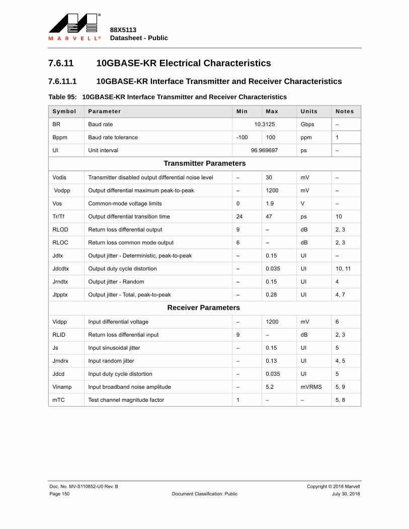
88X5113 Datasheet - Public
Doc. No. MV-S110852-U0 Rev. B Copyright © 2018 Marvell
Page 150 Document Classification: Public July 30, 2018
7.6.11 10GBASE-KR Electrical Characteristics
7.6.11.1 10GBASE-KR Interface Transmitter and Receiver Characteristics
Table 95: 10GBASE-KR Interface Transmitter and Receiver Characteristics
Symbol Parameter Min Max Units Notes
BR Baud rate 10.3125 Gbps –
Bppm Baud rate tolerance -100 100 ppm 1
UI Unit interval 96.969697 ps –
Transmitter Parameters
Vodis Transmitter disabled output differential noise level – 30 mV –
Vodpp Output differential maximum peak-to-peak – 1200 mV –
Vos Common-mode voltage limits 0 1.9 V –
Tr/Tf Output differential transition time 24 47 ps 10
RLOD Return loss differential output 9 – dB 2, 3
RLOC Return loss common mode output 6 – dB 2, 3
Jdtx Output jitter - Deterministic, peak-to-peak – 0.15 UI –
Jdcdtx Output duty cycle distortion – 0.035 UI 10, 11
Jrndtx Output jitter - Random – 0.15 UI 4
Jtpptx Output jitter - Total, peak-to-peak – 0.28 UI 4, 7
Receiver Parameters
Vidpp Input differential voltage – 1200 mV 6
RLID Return loss differential input 9 – dB 2, 3
Js Input sinusoidal jitter – 0.15 UI 5
Jrndrx Input random jitter – 0.13 UI 4, 5
Jdcd Input duty cycle distortion – 0.035 UI 5
Vinamp Input broadband noise amplitude – 5.2 mVRMS 5, 9
mTC Test channel magnitude factor 1 – – 5, 8

Electrical SpecificationsSERDES Electrical Specifications
Copyright © 2018 Marvell Doc. No. MV-S110852-U0 Rev. B
July 30, 2018 Document Classification: Public Page 151
Note
The load is 100Ω differential for these parameters, unless otherwise specified.
Defines the allow able reference clock difference and Rx baud rate tolerance relative to nominal. Tx baud rate is derived from multiplication of the reference clock (0 ppm delta).
Defined from 50 MHz to 2.5 GHz.
For 2.5 GHz -7.5 GHz RLOD>9-12log(Frequency/2.5)[dB] (Frequency defined in GHz).
For 2.5 GHz -7.5 GHz RLOC>6-12log(Frequency/2.5)[dB] (Frequency defined in GHz).
For 2.5 GHz -7.5 GHz RLID>9-12log(Frequency/2.5)[dB] (Frequency defined in GHz).
Relative to 100Ω differential and 25Ω common mode. Return loss includes contributions from on-chip circuitry, chip packaging, and off-chip optimized components related to the transmitter/receiver breakout.
Defined with a Bit Error Rate (BER) of 10^-12.
Defined for interference tests according IEEE 802.3 Annex 69A. For informative interconnect characteristics, refer to IEEE 802.3 Annex 69B.
Vidpp refers to the peak-to-peak.
The output Tx jitter is defined w hen applying the effect of a single-pole high-pass filter on the jitter. The high-pass filter 3 dB point is located at 4 MHz.
mTC describes the insertion loss transmission magnitude relative to the maximal allowed fitted attenuation mask Amax over a predefined frequency range. Defined for test1. The value for test2 is 0.5.
The receiver tolerates noise at an amplitude specified under receiver interference tolerance test1.The value for test2 is 12 mV.
Jdcdtx is included as a part of Jdtx.
Defined for a 1010 pattern and includes the entire range of emphasis.
The transmitter output waveform follows IEEE requirements as specified in section 72.7.1.10 Transmitter output waveform requirements.
Table 96: 10GBASE-KR Settings and Configuration
Parameter Setting/Configurat ion
Viddp The Viddp is the input differential voltage.The maximum single-ended voltage (common mode voltage and swing voltage) must not exceed 1.8V.
Output Equalization
The default as determined by the IEEE is 3 TAP FIR optimized per interconnect. 3 TAP FIR capabilities comply with the IEEE 802.3 standard section 72.7.1.10 Transmitter Output Waveform. For FIR control information, refer to the Functional Specifications.
NOTE: For further information, refer to the Functional Specifications.

88X5113 Datasheet - Public
Doc. No. MV-S110852-U0 Rev. B Copyright © 2018 Marvell
Page 152 Document Classification: Public July 30, 2018
7.6.11.2 10GBASE-KR Interface Transmitter Output Voltage Limits and Definitions
Figure 51: 10GBASE-KR Interface Transmitter Output Voltage Limits and Definitions
Figure 52: 10GBASE-KR Transmitter Output Differential Amplitude and Eye Opening

Electrical SpecificationsReference Clock
Copyright © 2018 Marvell Doc. No. MV-S110852-U0 Rev. B
July 30, 2018 Document Classification: Public Page 153
7.7 Reference Clock
Figure 53: Reference Clock Input Waveform
Table 97: Reference Clock (Over full range of values listed in the Recommended Operating Conditions unless otherwise specified)
Symbol Parameter Condit ion Min Typ Max Units
FCLK Clock Frequency1
1. CLKP/N must have an external AC-coupling capacitor.
-100 ppm 156.25 +100 ppm MHz
TR, TF Rise and Fall Times 20 to 80% of VPPD – 0.5 0.8 ns
VPPD Peak-to-Peak Differential Voltage
0.4 0.8 1.2 V
ZIND Input Impedance Differential 80 100 120 Ω
ZINC Input Impedance Common Mode – 100K – Ω
TDUTY Duty Cycle 45 50 55 %
JRMS RMS Jitter Integrated from 12 KHz to 20 MHz2
2. Specification assumes that there are no spurs in the phase noise plot.
– 0.17 0.5 ps
VIN Max
VIN Min
ClkP
ClkN
VICM VPP
VPPD = 2 * (VClkN – VClkP)

88X5113 Datasheet - Public
Doc. No. MV-S110852-U0 Rev. B Copyright © 2018 Marvell
Page 154 Document Classification: Public July 30, 2018
7.8 Output 25 MHz Clock
Table 98: Output 25 MHz Clock (Over full range of values listed in the Recommended Operating Conditions unless otherwise specified)
Symbol Parameter Condition Min Typ Max Units
FCLK Clock Frequency – – 25 – MHz
JRMS RMS Jitter – – 500 – ps, rms
VDIFF Differential Amplitude Peak-to-Peak
–760 780 800
mV
TR/TF Rise/Fall Time 2 pF, 50Ω termination/load
100 115 130ps

Electrical SpecificationsLatency
Copyright © 2018 Marvell Doc. No. MV-S110852-U0 Rev. B
July 30, 2018 Document Classification: Public Page 155
7.9 LatencyThe transmit latency is measured from the input of the PPM FIFO to the SERDES transmit pin.
The receive latency is measured from the SERDES receive pin to the input of the PPM FIFO.
The total latency in each direction is the sum of receive and transmit latency in the path.
Table 99: Chip Pin-to-pin Latency (Rx + Tx)
Parameter Latency Variation
(Dynamic) Latency Jit ter
Min Typ Max
1G PCS (1 lane) – – – 194.96 –
2.5G PCS (1 lane) – – – 74.95 –
5G PCS (1 lane) – – – 313.36 –
10G PCS - No FEC (1 lane) – – – 144.52 –
10G PCS - KR FEC (1 lane) – – – 434.07 –
25G PCS - No FEC (1 lane) 22 3.8 57 70 79
25G PCS - KR FEC (1 lane) 22 3.8 172 186 194
25G PCS - RS FEC (1 lane) 46 24.3 456 484.6 502
40G PCS - No FEC (4 lane) 33 17.6 167 180 200
40G PCS - KR FEC (4 lane) 32 17.6 455 468 487
50G PCS - No FEC (4 lane) 0 14.08 – 143.6 –
50G PCS - KR FEC (4 lane) 0 14.08 – 374.5 –
50G PCS - No FEC (2 lane) 0 14.08 – 139.89 –
50G PCS - KR FEC (2 lane) 0 14.08 – 372.02 –
50G PCS - RS FEC (2 lane) 0 14.08 – 360.85 –
100G PCS - No FEC (4 lane) 39 4.5 134 151 173
100G PCS - RS FEC (4 lane) 44 4.5 215 246 259

88X5113 Datasheet - Public
Doc. No. MV-S110852-U0 Rev. B Copyright © 2018 Marvell
Page 156 Document Classification: Public July 30, 2018
8 Mechanical Drawings
8.1 Package Mechanical Drawings
Figure 54: 169-pin FCBGA 14 × 14 Package Mechanical Drawings — Top and Side View

Mechanical DrawingsPackage Mechanical Drawings
Copyright © 2018 Marvell Doc. No. MV-S110852-U0 Rev. B
July 30, 2018 Document Classification: Public Page 157
Figure 55: 169-pin FCBGA 14 × 14 Package Mechanical Drawings — Bottom View

88X5113 Datasheet - Public
Doc. No. MV-S110852-U0 Rev. B Copyright © 2018 Marvell
Page 158 Document Classification: Public July 30, 2018
Table 100: 169-pin FCBGA (14 mm × 14 mm) Package Dimensions
Symbol
Dimension in mm
Min Nom Max
Total Thickness A 2.770 2.890 3.010
Stand Off A1 0.400 -- 0.600
Substrate Thickness A2 0.940 REF
Thickness from Substrate Surface to Die Backside
A3--- REF
Body Size D 14.000 BSC
E 14.000 BSC
Ball Diameter 0.600
Ball Width b 0.500 --- 0.700
Ball Pitch e 1.000 BSC
Ball Count n 169
Edge Ball Center to Center D1 12.000 BSC
E1 12.000 BSC
Expose Die Size D2 ---
E2 ---
Package Edge Tolerance aaa 0.100
Substrate Parallelism bbb ---
Top Parallelism ccc 0.200
Coplanarity ddd 0.150
Ball Offset <Package> eee 0.250
Ball Offset <Ball> fff 0.100

Order InformationOrdering Part Numbers and Package Markings
Copyright © 2018 Marvell Doc. No. MV-S110852-U0 Rev. B
July 30, 2018 Document Classification: Public Page 159
9 Order Information
9.1 Ordering Part Numbers and Package MarkingsFigure 56 shows the ordering part numbering scheme for the 88X5113 device.
Figure 56: Sample Part Number
xx – xxx 4 x000 - T123
Part Number
88X5113
Package Code
BVW = 169-pin FCBGA
Environmental
4 = Green+ Lead-free bumps
Temperature Range
C = CommercialI = IndustrialCustom Code
Custom (optional)
88X5113 –
Custom Code
Table 101: 88X5113 Part Order Option
Package Type Part Order Number
88X5113 169-pin FCBGA 14 × 14 - Commercial 88X5113-XX-BVW4C000
88X5113 169-pin FCBGA 14 × 14 - Industrial 88X5113-XX-BVW4I000
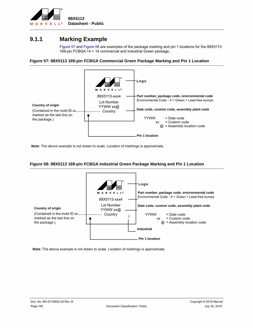
88X5113 Datasheet - Public
Doc. No. MV-S110852-U0 Rev. B Copyright © 2018 Marvell
Page 160 Document Classification: Public July 30, 2018
9.1.1 Marking ExampleFigure 57 and Figure 58 are examples of the package marking and pin 1 locations for the 88X5113 169-pin FCBGA 14 × 14 commercial and industrial Green package.
Figure 57: 88X5113 169-pin FCBGA Commercial Green Package Marking and Pin 1 Location
Figure 58: 88X5113 169-pin FCBGA Industrial Green Package Marking and Pin 1 Location
88X5113-xxx4
Lot NumberYYWW xx@
Country
Country of origin
(Contained in the mold ID or marked as the last line on the package.)
Note: The above example is not drawn to scale. Location of markings is approximate.
Logo
Part number, package code, environmental codeEnvironmental Code - 4 = Green + Lead-free bumps
Date code, custom code, assembly plant code
YYWW = Date codexx = Custom code
@ = Assembly location code
Pin 1 location
88X5113-xxx4
Lot NumberYYWW xx@
Country
Country of origin
(Contained in the mold ID or marked as the last line on the package.)
Note: The above example is not drawn to scale. Location of markings is approximate.
I
Logo
Part number, package code, environmental codeEnvironmental Code - 4 = Green + Lead-free bumps
Date code, custom code, assembly plant code
YYWW = Date codexx = Custom code
@ = Assembly location code
Pin 1 location
Industrial

Copyright © 2018 Marvell Doc. No. MV-S110852-U0 Rev. B
July 30, 2018 Document Classification: Public Page 161
A Revision History
Table 102: Revision History
Revision Date Sect ion Detai l
Rev. B July 30, 2018 All applicable Initial release

Marvell. Moving Forward Faster
Marvell Technology Group http://www.marvell.com
Back Cover