8096
DESCRIPTION
ARCHITECTURE OF 8096, MEMORY ORG, ARMTRANSCRIPT

Introduction
The 8096 is a 16 bit microcontroller. It is specially suited for embedded control applications.
It has all the features of 8051, except bit addressing and bit manipulation. The additional features present in 8096 are A/D converter, high speed
inputs, and high speed outputs, generation of analog output analog voltage and mechanism for self-checking in runtime.
It has a powerful instruction set and addressing modes.
Features of 8096
(i) It is a 16 bit microcontroller.(ii) 8096 is been designed for high speed/high performance control applications.(iii) It has 8 multiplexed input analog to digital converter with 10 bit resolution.(iv) The high speed I/O section of 8096 comprises a 16 bit timer, a 16 bit counter
and 4 input programmable edge detector, 4 software timers and 6 output programmable event generator.
(v) Its serial port support different modes of operation with programmable baud rates.
(vi) It supports register to register architecture which increases processing speed.(vii) It is programmable pulse width modulation (PWM) output signals can be used
as control signals to drive a motor or any other application.(viii) It has 100 instructions that can operate on bit, byte, word, double words.(ix) It consists of a complete set of 16 bit arithmetic instructions that include
multiply and divide operations.(x) It allows bit operations. They are done on any bit in the register file or in the
special function register.(xi) Logical are arithmetic instructions support byte and word operations.(xii) The watchdog timer can be used to reset the system if software fails to
operate properly.Architecture
The 8096 family of microcontrollers has several sections, all of which work in an integrate manner to obtain high performance computing and control.
The major sections include a 16 bit CPU, a programmable high speed input/output unit, on-chip RAM, on-chip ROM, analog to digital converter, serial port and pulse-width modulated output for analog to digital converter.
Figure shows the internal architecture of 8096 microcontroller. It consists of several functional units. They are.
(i) CPU with 232 byte register file and register ALU.(ii) 8KB internal ROM.(iii) Programmable high speed I/O unit.(iv) Two 16 bit timers/counters.(v) Serial ports.(vi) Pulse width modulator.
8096 Microcontroller

(vii) Watchdog timer(viii)Memory controller.(ix) Eight multiplexed inputs A/D converter with 10 bit resolution.
8096 Architecture Block Diagram The two main buses address bus and data buses are used for inter-processor
communication. The address bus is 8 bit and data bus is 16 bit. The data bus transfers data between RALU and register file or special
function registers. (SFRs). The address bus provides addresses for multiplexed address/data bus
connecting to the memory controller. The memory controller provides the addresses for the internal ROM and
external memory.
Memory Organization
The 8096 can access upto 64 KB memory. The scratch pad register (called as register file), special function registers, on-chip RAM, on-chip ROM and external memory space are the main constituents of memory.
Figure shows the map of 64kB addressable memory space.The basic blocks are:
(i) Internal RAM containing
(a) Special function registers (00 to 17H).(b) Stack pointer (18H and 19 H)(c) Register file (1AH to EFH) (d) Power down RAM (F0H to FFH)

This memory area is accessed as data memory. No code can be executed from this area. The program memory area of 00 to FFH is reserved for internal use of Intel development systems.
(ii) Internal ROM
If the chip has on-chip ROM then it has interrupt vectors, factory test code, and internal program storage. It is available at addresses (2000H – 3FFFH).
If the chip does not contain ROM, then these are defined in the external memory.
(iii) External memory or I/O are available at addresses (0100H – 1FFDH) and (4000H – FFFFH).
(iv) Port 3 and 4 locations (1FFEH and 1FFFH) for the reconfiguration if they are not used as address/data lines.
When the 8096 is reset, address 2080H is loaded to the program counter to give 8 KB of contiguous memory.
Memory Map
CPU Section
The central processing unit is responsible for processing arithmetic and logical operations and for generation of control signals.
The different control signals are generated depending on the instruction being executed.
The CPU comprises of the following :(i) Register file(ii) Register Arithmetic and logic unit (RALU)(iii) Control unit.
Register File
The following figure shows the complete internal RAM memory map.

The CPU register file has 256 bytes of memory from location 00H to FFH. No code can be executed from these CPU register file locations. If an
attempt is made to execute instructions from these locations, the instructions will be automatically fetched from the external memory.
Two 8 bit temporary registers are provided by CPU hardware. They are used to access the locations from the CPU file.
Internal Ram Structure in 8096
Of the 256 locations, first 24 memory locations 00H – 17H are special function registers (SFRs).
SFRs are used to control the on-chip I/O section. The remaining 232 are RAM locations. These locations can be accessed as
bytes, words or double words. Each of these 232 locations can be used by the RALU. Hence, there are 232
accumulators. The first word in the RAM locations 18H and 19H is stack pointer. They can
be used as part of the register file if stack operation is not done. The stock pointer must be initialized by user program. It can point anywhere in 64 KB (external) memory space.
The upper 16 bytes (0F0 – 0FFH) are kept alive, even when the power fails. This feature is described under power down RAM. These locations receive their power from VPD pin in power down mode. Hence, only in the power down mode these locations are alive.

Special Function Registers (SFRs)
The CPU communicates with the other resources of 8096 through special function registers (SFRs) defined in the internal RAM space 00H – 19H.
Through these SFRS, the CPU controls the various timers, high speed I/O points, interrupts, ADC, stack and I/O ports.
Figure shows the locations and names of SFRs. Many of the SFRs service two functions, one if they are read and other if they are written.
CPU Buses
There are two buses A (address) and D (data) bus. The different units of CPU interact with each other through these buses.
The address bus is 8 bit wide and data bus is 16 bit wide. Data bus is used for sending/receiving data information.
The reason for making address bus 8 bit wide is that internal on-chip RAM containing SFRs and register file is 256 bytes long and can be directly addressed by using on 8 bit address.
For 16 bit transfer two memory cycles will be needed.
RALU
The register arithmetic and logic unit (RALU) contains :(i) 17 bit ALU(ii) Program counter + incrementer.(iii) Program status word.(iv) Loop counter (5 bit).(v) Two shift registers (17 bit).(vi) Temporary registers (17 bit).
For instruction requiring shift for execution, shift registers are provided. e.g. : shift left, shift right, normalize, multiply, divide etc.

When a 16 bit data is to be shifted, an upper word register/shifter is used. The lower word/shifter is used along with upper word register/shifter in case of 32 bit shift.
For the instructions that require repetitive shifts (e.g. shift right by 5 bits), a 5 bit loop counter is useful.
For execution of two operand instructions, a temporary register is provided. This temporary register stores the multiplier during the execution of multiplication instruction, or divisor during execution of division instruction.
For the execution of increment/decrement instructions some constants are defined. The constants 0, 1, 2 are stored in RALU to execute the instruction faster.
The A bus (address bus) is 8 bit wide. It is used to transfer 16 bit address or data information to memory controller or other units. A delay circuit is provided. It facilitates transfer of lower byte followed by delay followed by upper byte to the memory controller.
Program counter and incrementer are provided in RALU to increment the PC after execution of each instruction. Thus, it points to the next instruction to be executed.
In case of jump instructions being executed, the program counter is modified through ALU.
Program Status Word
The program status word signifies the status of interrupt flags as well as condition flags at any instant.
15 14 13 12 11 10 9 8 7 6 5 4 3 2 1 0
Z N V VT C – I ST Interrupt Mask Register
Program Status Word (PSW)Z: Indicates that the result of last arithmetic/logic instruction was zero.N: Indicates that the last instruction generated negative result.V: Result generated in outside the range that can be expressed in the
destination data type thus causing overflow.VT: When the V flag is set, VT (overflow trap) is also set. However, it can be reset
by certain explicit instructions. It is useful in debugging the program.C: Indicates that a bit is shifted out of MSB or ISB position because of arithmetic
or shift operations.ST: Can be used for controlling rounding after right shift called “sticky bit”. It
indicates that 1 has been shifted first to c flag and then out during right shift.I: It is set by EI instruction and cleared by DI instruction. It indicates global
interrupt enable/disable.These conditional flags (except I) can be used in conditional jump instructions.
Control Unit
The control unit contains the instruction register, the decoder and timing unit to generate various control signals. The instruction is transferred to the control unit through A bus and is stored in the instruction register. The instruction is decoded and the required signals are generated for RALU control.

Memory Controller
The memory controller is used as the interface between RALU and external memory or on-chip ROM.
The 8 bit wide address bus is used to transfer the address and data between RALU and memory controller.
Whenever RALU wants an instruction/data from memory it should send the lower byte of address on address bus followed by the upper byte of address.
The memory controller interacts with the external memory through an external address/data bus AD0 – AD15 (ports 3, 4).
I/O SECTION All of the on-chip I/O feature of 8096 can be accessed through the special
function registers. There are seven major I/O functions.
Major I/O Functions
I/O functionsHigh speed input unit Provides Automatic recording of events.High speed output unit
Provides automatic triggering of events and real time interrupts.
Pulse width modulation
Output to drive motors or analog circuits.
A to D converter Provides analog to digital conversionWatchdog Timer Resets 8096 if a malfunction occurs.Serial port Provides synchronous or asynchronous link.Standard I/O lines Provide interface to external world.
Timers
There are two 16 bit-timers: Timer 1 and Timer 2. Timer 1 is a 16 bit free running timer. It is used to synchronize events to real
time. Timer 2 can be clocked externally. It synchronizes events to external
occurrences. The high speed I/O unit is coupled to the timers. HSI records the value when
transitions occurs on timer 1. HSO causes transitions to occur based on values of Timer 1 or Timer 2.
Timer 1
Timer 1 is used to provide real time clock for external events that are recorded on High Speed Input (HSI) lines or which are generated on High Speed Output (HSO) lines of 8096.
The input clock is i.e. it is clocked once every eight state times. (e.g. : for a 12 MHz, the state time is 0.25 s. Hence period of Timer 1 clock is 2 s).
It can be reset only by executing a reset. The only other way to change its value is by writing to 000CH. But it is a test
mode that sets both the timers to 0FFFXH and should not used in programs.
Timers 2
Timer 2 is an event counter as if uses an external clock source. It can have on of following sources as clock :

(i) Timer 2 clock (port p 2.3)(ii) High speed input line no. 1.
The selection of clock source can be done by the user programming the bit 7 of I/O control register 0. (IOC0.7).
Timer 2 is used for generating high speed outputs. The maximum speed of timer 2 is once per eight state times.
Timer 2 is incremented by transitions (one count by each falling edge or rising edge).
Timer 2 can be reset by the following methods.(i) by executing a reset.(ii) by setting IOC0, 1(iii) triggering the HSO channel 14 (0EH).(iv) by setting HIS.0 = 1 or IOC0.3 = 1 and pulling TRST.
Figure shows different methods of manipulating Timer 2.
Timer 2 Clock and Reset Options
Timer Interrupts
The two Timers 1 and Timer 2 can be used to trigger a timer overflow interrupt and set a flag in the I/O status register 1 (IOS1). The interrupts are controlled by IOC1.2 and IOC1.3.
The flags are set in IOS1.5 and IOS1.4. The enabling and disabling of timer interrupts are controlled by the interrupt mass register bit 0. In all cases, setting a bit enables a function while clearing a bit disables it.
High Speed Inputs (HSI)
The HSI unit can be used to record the time at which an event occurs with respect to Timer 1.
There are 4 lines. (HSI.0, HSI.1, HSI.2 and HSI.3). These are used in this mode to record up to 8 events.
HSI.2 and HSI.3 are bidirectional pins. They can be used as HSO.4 and HSO.5.
The I/O control registers IOC0 and IOC1 are used to determine the functions of these pins.

Fig. 15.6.2 shows HSI unit block diagram.
HSI Unit
It can measure pulse widths and record times of events with a 2s resolution.
HSI Modes
For each HSI there are 4 modes of operation. The HSI mode register is used to control the pins that look for type of events.
Fig. 15.6.3 shows the HSI mode register.
Where each 2-bit mode control fieldDefines one of 4 possible modes:00 8 positive transitions01 Each positive transition10 Each negative transition11 Every transition (Positive and negative)HSI Mode Register
The information is then stored in a sevel level FIFO for later retrieval. High and low levels of inputs require to be held for 1 state time to ensure
proper operation. The maximum input speed is 1 event every 8 state times except when the
8 transition mode is used, is which one transition per state is allowed. The HSI lines can be enabled and disabled using bits IOC0 at location 0015H.
HSI FIFO
When an HSI event occurs, a 8 20 FIFO stores the 16 bits of Timer 1 and 4 bits indicating the state of 4 HSI lines at the time the status is read.

It can take up to 8 state times for the information to reach the holding register. Hence, 8 state times are allowed between consecutive reads of HSI_TIME.
When the FIFO is full, an additional event for a total of 8 events can be stored considering the holding register as a part of FIFO.
If the FIFO and holding register are full, any additional event will not be recorded. It will cause an overflow condition.
HSI Interrupts
HSI unit generates interrupts in one of two methods determined by IOC1.7. If a bit is 0, then an interrupt is generated each time a value is loaded in to
the holding register. If bit is 1 an interrupt is generated when the FIFO has six entries in it.
All the interrupts are rising edge triggered. Hence, if IOC1.7 = 1 then the processor will not be re-interrupted till the FIFO contains 5 or less records.
The interrupts can also be generated by HSI.0 pin that has its own interrupt vector location 2008H. Thus, an HSI unit generates interrupts in 3 methods.
HSI Status
The status of HSI FIFO is shown by bits 6 and 7 of the I/O status register 1 (IOS1).
If bit 6 is 1, the FIFO contains at least 6 entries. If bit 7 is 1, the FIFO contains at least one entry and the holding register has been located.
The FIFO can be read after verifying it contains valid data. While reading or testing bits in IOS1 it is essential to store the byte and then test the stored value.
The HSI can be read in two steps. Initially the HSI status register is read in order to obtain the current state of the HSI pins and which pins have changed at the recorded time.
Figure shows the HSI status register.
Where for each 2 bit status field the low bit indicates whether or not an even has occurred on this pin at the time in HSI time and the upper bit indicates the current status of the pin.
Then the HSI time register is read. Reading the time register unloads one word of the FIFO, so if the time register is read before the status register, the information in the status register is lost.
It is at location 06 H. The HSI time registers are at located 04 and 05H. If the HSI time and status registers are read without the holding register
being loaded, the values read will be undeterminable.
HSO CAM
Figure shows block diagram of HSO unit.

High Speed Output Unit
A content addressable memory file is the main component of the HSO. It stores up to 8 events that are pending to occur. Every state time one location of CAM is compared with the two timers. After 8 state times, the entire CAM is been searched for time matches.
If a match occurs a specified event will be triggered and that location of CAM will be made available for another pending event.
Each CAM register is 23 bits wide. Fig. 15.6.7 shows the format of command to HSO unit.
HSO Command Tag Format
To enter a command into CAM file, write 7 bit command tag to location 0006H followed by time at which action is to be carried into word address 0004H.
It is essential to disable interrupts while writing a command tag for HSO. If an interrupt occurs during the time between writing the command tag and loading the time value, then the ISR writes to HSO time register. The command tag is written to CAM. The command tag from main program will not be executed.
HSO Interrupts
The HSO unit can generate two type of interrupts. The HSO execution interrupts and the timer interrupt.
The HSO execution interrupts (vector = 2006 H) is generated when HSO commands operate one or more of six output pins. However it is a maskable interrupt.
The software timer interrupt is generated by any other HSO command like triggering the A/D, resetting Timer 2 or generating software delay.
HSO Status
The holding register must be empty before writing to HSO. If the holding register is not empty, it will overwrite value in the holding register.
The I/O status register (IOS0) bits 6 and 7 indicted status of HSO unit.

If IOS0.6 = 0, holding register is empty and atleast one CAM register is empty.
If IOS0.7 = 0, the holding resister is empty.
Clearing HSO
All 8 CAM locations are compared before any action is taken. It allows a pending external event to be cancelled by writing the opposite event to the CAM.
However, if an entry is placed in the CAM it cannot be removed till either the specified timer matches the written values or chip is reset.
Internal events are not synchronized to timer 1. Hence they cannot be cleared.
It includes events on HSO channels 8 through F and all interrupts. The interrupts are not synchronized. Hence, it is possible to have multiple interrupts at same time.
Using Timer 2 with HSO
The timer 1 is incremented once every 8 state times. If it is being used as a reference timer for the HSO action, then the comparator can observe all 8 CAM registers before Timer 1 changes its value.
Timer 2 is synchronized to allow it to change to a maximum rate of once per 8 state times.
The Timer 2 increments on both the edges of the input signal. If Timer 2 is used as a reference, care must be taken that the Timer 2 is not
reset prior to highest value for a Timer 2 match in the CAM because HSO CAM holds the pending event till a time match occurs. If match is not reached then the event remains pending in the CAM fill the 8096 is reset.
When Timer 2 is reset using HSO unit additional, care must be taken. This is because the HSO event is an internal event. It can happen at any time in the eight state time window.
If two events are scheduled such that they must occur at the same time as the Timer 2 reset then they must be logged into the CAM with a Timer value of zero.
If this method is used to design a programmable modulo counter, the count will remain at the maximum value of Timer 2 till a reset Timer 2 command is given.
The count remains zero for a transition that would change the count value from “N” to zero and then change on the next transition.
Software Timers
At present times the HSO can be programmed to generate interrupts. At a time four software interrupts can be used.
A software Timer flag is set by the HSO unit every time a programmed time is reached. An interrupt will be generated if the interrupt bit in the command tag is set. The Interrupt Service Routine (ISR) can then observe the contents of the I/O status register 1 (IOS1) to tell which of the software timers has expired and generated the interrupt.
When the HSO resets Timer 2 or starts an A / D conversion it can be programmed to generate a software timer interrupt. There is no flag to indicate the occurrence of event.

Multiple interrupts can also be generated.
Pulse Width Modulation Output
Figure shows the block diagram of a pulse width modulation circuit. It comprises of PWM register, PWM counter and comparator.
Pulse width modulated circuit
The PWM output is set to one when the counter value is zero. The 8 bit is incremented every state time. If the counter value matches with
the value in the PWM register the output is switched low. Incase the counter overflows the output is again switched high. The output is low when the value of PWM register is 00. The output
waveform is variable duty cycle pulse that repeats every 256 state times. (64 s at 12 MHz).
By writing the PWM register at location 17H, changes are made in the duty cycle.
Normally motors need PWM waveform for efficient operation. If the PWM waveform is integrated it produces a DC level that can be changed in 256 steps by modifying the duty cycle.
A Port 2 pin5 is shared with the PWM output. Hence, both these features cannot be used at the same time. The PWM function is selected by IOC01. 0 bit is set.

PWM outputs
Serial Port
The 8096 has an on-chip serial port to minimize the number of chips needed in the system.
It has one synchronous and three asynchronous modes. In the asynchronous modes baud rate of upto 18.5 Kbaud can be used while
in asynchronous mode baud rates upto 1.5 Mbaud are available. The chip has a baud rate generator that is independent of Timer 1 and Timer
2. The asynchronous modes are full duplex i.e. they can simultaneously
transmit and receive. Also they are double buffered i.e. they can begin reception of the second data byte before a previously received byte has been read from the receive register.
The serial port registers used for transmission and reception are SBUFTx and SBUFRx. Both these registers share same address 07H. They are physically separate.
The SBUFTx register hold data that is ready for transmission while SBUFRx register has data that is received by the serial port.
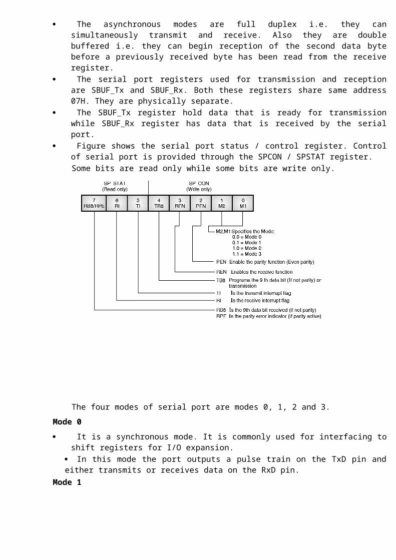
Figure shows the serial port status / control register. Control of serial port is provided through the SPCON / SPSTAT register.Some bits are read only while some bits are write only.
The four modes of serial port are modes 0, 1, 2 and 3.
Mode 0
It is a synchronous mode. It is commonly used for interfacing to shift registers for I/O expansion.

In this mode the port outputs a pulse train on the TxD pin and either transmits or receives data on the RxD pin.
Mode 1 It is standard asynchronous mode; 8 bits plus a stop bit and start bit are sent
or received. Hence, total frame size is of 10 bits. If parity is enabled (PEN = 1) then an even parity bit is transmitted instead
of 8th data bit.
It is commonly used for CRT terminals. Mode 2
It is an asynchronous 9th bit recognition mode. 11 bit frames are transmitted through the TxD and are received through RxD
start bit 0, 8 data bits, a programmable 9th bit and one stop bit. A 0 or 1 can be assigned to the 9th data bit using the 88 bit in control
register before writing to SBUFTx. This bit can be used to provide a selective reception on the data link.
The serial port interrupt and receive interrupt (RI) will not be activated till the 9th received bit is 1 during the reception of data.
Mode 2 is used with 3 for multiprocessor communication.
Mode 3
It is also an asynchronous 9th bit mode. 11 bit frames a transmitted with one start bit, 8 data bits, a programmable 9th bit and one stop bit. 11 bit data frame is identical to data frame of mode 2.
The only difference is that the 9th bit becomes a parity bit. If parity is not enabled (PEN = 0), the TBS controls the status of ninth transmitted bit. It must be set before each transmission. On reception, if PEN = 0, the RB8 bit indicates the state of the ninth received bit.
If the parity is enabled i.e. PEN = 1 then the same bit is called (RPE) receive parity error. It is used to indicate a parity error.
Multiprocessor Communication
Modes 2 and 3 can be used for multiprocessor configuration.

Multiprocessor communication If the 9th received bit is not set in mode 2 then the serial port interrupt is not
activated. This feature is used in multiprocessor systems. When the master processor wishes to transmit a block of data to one of its
several slaves then it first sends an address frame that identifies the target slave.
An address frame will differ from the data frame by the 9th data bit. If the 9th
data bit is 1 then it is an address frame, if bit is 0 then it is a data frame. A data frame does not interrupt a slave in mode 2. However an address
frame interrupts all slaves so that each slave can examine the received byte and observe if it is being addressed.
The addressed slave will switch to mode 3 in order to receive the coming data frames. The slaves that were unaddressed remain in mode 2 and do not receive any byte.
Determining Baud Rates
The baud rates for all the modes are controlled with the help of a baud rate register. It is a byte wide register that is sequentially loaded with two bytes. It internally stores the value as a word.
The least significant byte is loaded to the register followed by the most significant byte.
The most significant byte of the baud value determines the clock source for the baud rate generator.
If a bit is one, the XTAL1 pin is used as source, if bit is zero, the T2 CLK pin is used.The baud rate formulas are given below:Using XTAL1Mode 0: Baud rate = ; B0Others: Baud rate =Using T2 CLKMode 0: Baud rate = ; B0Others: Baud rate = ; B0
Note: B cannot be equal to 0, except when using XTAL1 in other mode than mode 0.
The variable “B” is used to represent the least significant 15 bits of the value loaded into the baud rate register. The maximum value of B is 32767. Table 15.6.2 gives baud rates for values 10, 11, 12 MHz
I/O Ports 0, 1, 2, 3 and 4
8096 has five 8 bit I/O ports. Some of them are input ports while some of the ports are output ports and other ports are bidirectional and have alternate functions.
The input ports connect to the internal bus through an input buffer. The output ports connect through the output buffer to an internal register
that holds the output bits. Bi-directional ports comprise of an internal register, an input buffer and an
output buffer. When an instruction accesses a bidirectional port as source register, the
value comes from the port pins, not the internal register.
Port 0
Port 0 is an input port. It shares its pins with the analog inputs to the A/D converter.
Port 1
A is a quasi-bidirectional I/O port. The word “quasi-bidirectional” means that the port pin has a weak internal pull up that is always active and an internal pull-down than can be on/off.
The pin’s logic level can be controlled by an external pull-down if the internal
pull-down is left off. (i.e. a 1 is written). A quasi-bidirectional port will source current if externally held it. It will pull
itself high if it is left unconnected. If the processor writes to the pins of a quasi-bidirectional port it actually
writes into the register that drives the port pin. If the port pin is to be used as an input then the software must write a one to
SFR bit. This causes the low impedance pull down device to turn off and leave the pin pulled with a high impedance pull up device that can be driven by the device that drives the input.
Port 2
It is a multi-functional port.Port 2 functions
Port Function
Alternate Function Controlled by
P2.0 Output TxD (Serial Port Transmit) IOC1.5P2.1 Input RxD (Serial Port Receive) in
Model -3N/A
P2.1 Output RxD (Serial Output Port) in Mode 0
N/A
P2.2 Input External interrupt IOC1.1P2.3 Input T2CLK (Timer 2 input) IOC1.7P2.4 Input R2RST (Timer 2 Reset) IOC0.5P2.5 Output PWM (Pulse Width
Modulation)IOC1.0
P2.6 Quasi-bidirectional N/AP2.7 Quasi-bidirectional N/A
Ports 3 and 4/ AD0 – AD15
These pins serve as bidirectional ports with open drain outputs or system bus pins used by memory controller when it accesses external memory.
If the ––– line is low, it serves as system bus. If –––line is set then they are used as Ports.
A/D Converter
The A/D converter on 8096 provides 8 input channels with a 10 bit digital output.
The channels are multiplexed. For A/D conversion successive approximation method is used.
The digital output is equivalent to ratio of input voltage divided by the analog supply voltage. If ratio is unity then result is all ones.

A/D Conversion Time and Formula
On 8096 each conversion need 168 state times (42 s at 12 MHz) independent of accuracy of value of input voltage.
On 8096 BH each conversion requires 88 state times (22 s at 12 MHz) independent of accuracy or value of input voltage.
The analog input voltage should be in range of 0 to VRFF A/D result is calculated as,
=The change in VREF or ANGND effects the output of the converter. It is
advantageous if a radiometric sensor is used as these sensors have an output that can be measured in proportion of VREF.
Watchdog Timer (WDT)
The watchdog timer is a method of recovery from software upset. After it is initialised, if the software fails to reset the watchdog at least every
64 K state times, a hardware reset will be initiated. The system will not restart.
The watchdog timer is a 16 bit counter. It is incremented each and every state time. It is cleared by program after periodic interval. It is not allowed to overflow.
If a program does not properly progress then an overflow occurs. As a result of overflow the hardware causes the system to restart and prevents the controller from causing a malfunction for longer than 16 ms in case a 12 MHz oscillator is used.
In reset the watchdog timer can be disabled. A clear WDT instruction enables it. Code is first written to WDT register. The
timer is cleared by writting a “01EH” followed by “0E1H” to WDT register at memory location 00AH.
After WDT in initialized, it cannot be disabled by software. The only method to disable WDT is to hold the RESET pin at 2 to 2.5 volts.
Voltage above 2.5 V on pin can damage the WDT. Hence, this method is not recommended for normal operation. It is only used for debugging.
ADVANCED RISC MACHINES (ARM) PROCESSORS
The ARM7TDMI-S processor is a member of the ARM family of general-purpose 32-bit microprocessors. The ARM family offers high performance for very low-power consumption and gate count. The ARM7TDMI-S processor has Von Neumann architecture, with a single 32-bit data bus carrying both instructions and data. Only load, store, and swap instructions can access data from memory. The ARM7TDMI-S processor uses a three stage pipeline to increase the speed of
the flow of instructions to the processor. This enables several operations to take
place simultaneously, and the processing, and memory systems to operate
continuously.
ARM7TDMIS stands for
T: THUMB

D for on-chip Debug support, enabling the processor to halt in response to a
debug request,
M: enhanced Multiplier, yield a full 64-bit result, high performance
I: Embedded ICE hardware (In Circuit emulator)
S: Synthesizable
FEATURES OF ARM PROCESSORS The ARM processors are based on RISC architectures and this architecture
has provided small implementations, and very low power consumption. Implementation size, performance, and very low power consumption remain the key features in the development of the ARM devices.
The typical RISC architectural features of ARM are : A large uniform register file. A load/store architecture, where data-processing operations only operate on
register contents, not directly on memory contents. Simple addressing modes, with all load/store addresses being determined
from register contents and instruction fields only uniform and fixed-length instruction fields, to simplify instruction decode.
Control over both the Arithmetic Logic Unit (ALU) and shifter in most data-processing instructions to maximize the use of an ALU and a shifter
Auto-increment and auto-decrement addressing modes to optimize program loops
Load and Store Multiple instructions to maximize data throughput Conditional execution of almost all instructions to maximize execution
throughput.There are three basic instruction sets for ARM.
A 32- bit ARM instruction set A 16 –bit Thumb instruction set. The Thumb instruction set is a subset of the most commonly used32-bit ARM
instructions. Thumb instructions operate with the standard ARM register configurations, enabling excellent interoperability between ARM and Thumb states. This Thumb state is nearly 65% of the ARM code and can provide 160%of the performance of ARM code when working on a 16-bit memory system. This Thumb mode is used in embedded systems where memory resources are limited.
ARCHITECTURE OF ARM PROCESSORS: The ARM 7 processor is based on Von Neman model with a single bus for
both data and instructions (The ARM9 uses Harvard model).ARM uses the Advanced Microcontroller Bus Architecture (AMBA) bus architecture. This AMBA include two system buses: the AMBA High-Speed Bus (AHB) or the Advanced System Bus (ASB), and the Advanced Peripheral Bus (APB).
The ARM processor consists of Arithmetic Logic Unit (32-bit) One Booth multiplier(32-bit) One Barrel shifter One Control unit Register file of 37 registers each of 32 bits. In addition to this the ARM also consists of a Program status register of
32 bits, Some special registers like the instruction register, memory

data read and write register and memory address register ,one Priority encoder which is used in the multiple load and store instruction to indicate which register in the register file to be loaded or stored and Multiplexers etc.
ARM Registers: ARM has a total of 37 registers .In which - 31 are general-purpose registers of 32-bits, and six status registers .But all these registers are not seen at once. The processor state and operating mode decide which registers are available to the programmer. At any time, among the 31 general purpose registers only 16 registers are available to the user. The remaining 15 registers are used to speed up exception processing. there are two program status registers: CPSR and SPSR (the current and saved program status registers, respectively
In ARM state the registers r0 to r13 are orthogonal—any instruction that you can apply to r0 you can equally well apply to any of the other registers.
The main bank of 16 registers is used by all unprivileged code. These are the User mode registers. User mode is different from all other modes as it is unprivileged. In addition to this register bank, there is also one 32-bit Current Program status Register (CPSR).

In the 15 registers, the r13 acts as a stack pointer register and r14 acts as a link register and r15 acts as a program counter register.
Register r13 is the sp register, and it is used to store the address of the stack top. R13 is used by the PUSH and POP instructions in T variants, and by the SRS and RFE instructions from ARMv6.
Register 14 is the Link Register (LR). This register holds the address of the
next instruction after a Branch and Link (BL or BLX) instruction, which is the instruction used to make a subroutine call. It is also used for return address information on entry to exception modes. At all other times, R14 can be used as a general-purpose register.
Register 15 is the Program Counter (PC). It can be used in most instructions as a pointer to the instruction which is two instructions after the instruction being executed.
The remaining 13 registers have no special hardware purpose. CPSR: The ARM core uses the CPSR register to monitor and control internal
operations. The CPSR is a dedicated 32-bit register and resides in the register file. The CPSR is divided into four fields, each of 8 bits wide: flags, status, extension, and control. The extension and status fields are reserved for future use. The control field contains the processor mode, state, and interrupt mask bits. The flags field contains the condition flags. The 32-bit CPSR register is shown below.
Processor Modes: There are seven processor modes .Six privileged modes abort, fast interrupt request, interrupt request, supervisor, system, and undefined and one non-privileged mode called user mode.
The processor enters abort mode when there is a failed attempt to access memory. Fast interrupt request and interrupt request modes correspond to the two interrupt levels available on the ARM processor. Supervisor mode is the mode that the processor is in after reset and is generally the mode that an operating system kernel operates in. System mode is a special version of user mode that allows full read-write access to the CPSR. Undefined mode is used when the processor encounters an instruction that is undefined or not supported by the implementation. User mode is used for programs and applications.
Banked Registers: Out of the 32 registers, 20 registers are hidden from a program at different times. These registers are called banked registers and are identified by the shading in the diagram. They are available only when the processor is in a particular mode; for example, abort mode has banked registers r13_abt, r14_abt and spsr _abt. Banked registers of a particular mode are denoted by an underline character post-fixed to the mode mnemonic or _mode.

When the T bit is 1, then the processor is in Thumb state. To change states the core executes a specialized branch instruction and when T= 0 the processor is in ARM state and executes ARM instructions. There are two interrupt request levels available on the ARM processor core—interrupt request (IRQ) and fast interrupt request (FIQ).
V, C, Z , N are the Condition flags . V (overflow) : Set if the result causes a signed overflow C (Carry) : Is set when the result causes an unsigned carry Z (Zero) : This bit is set when the result after an arithmetic
operation is zero, frequently used to indicate equality N (Negative) : This bit is set when the bit 31 of the result is a binary 1.
PIPE LINE: Pipeline is the mechanism used by the RISC processor to execute instructions at an increased speed. This pipeline speeds up execution by fetching the next instruction while other instructions are being decoded and executed. During the execution of an instruction, the processor Fetches the instruction .It means loads an instruction from memory. And decodes the instruction i.e identifies the instruction to be executed and finally Executes the instruction and writes the result back to a register.
ARM Processor Families There are various ARM processors available in the market for different
application .These are grouped into different families based on the core .These families are based on the ARM7, ARM9, ARM10, and ARM11 cores. The numbers 7, 9, 10, and 11 indicate different core designs. The ascending number indicates an increase in performance and sophistication. Though ARM 8 was introduced during 1996, it is no more available in the market. The following table gives a brief comparison of their performance and available resources.
The ARM7 core has a Von Neumann–style architecture, where both data and instructions use the same bus. The core has a three-stage pipeline and executes the architecture ARMv4T instruction set. The ARM7TDMI was introduced in 1995 by ARM. It is currently a very popular core and is used in many 32-bit embedded processors. The ARM9 family was released in 1997. It has five stage pipeline architecture. Hence, the ARM9 processor can run at higher clock frequencies than the ARM7 family. The extra stages improve the overall performance of the processor. The memory system has been redesigned to follow the Harvard architecture, with separate data and instruction buses. The first processor in the ARM9 family was the ARM920T, which includes a separate D + I cache and an MMU. This processor can be used by operating systems requiring virtual memory support. ARM922T is a variation on the ARM920T but with half the D +I cache size. The latest core in the ARM9 product line is the ARM926EJ-S synthesizable processor core, announced in 2000. It is designed for use in small portable Java-enabled devices such as 3G phones and personal digital assistants (PDAs).

The ARM10 was released in 1999 . It extends the ARM9 pipeline to six stages. It also supports an optional vector floating-point (VFP) unit, which adds a seventh stage to the ARM10 pipeline. The VFP significantly increases floating-point performance and is compliant with the IEEE 754.1985 floating-point standard The ARM1136J-S is the ARM11 processor released in the year 2003 and it is designed for high performance and power efficient applications. ARM1136J-S was the first processor implementation to execute architecture ARMv6 instructions. It incorporates an eight-stage pipeline with separate load store and arithmetic pipelines.
A brief comparison of different ARM families is presented below:
ARM Family
Year of Release
Architecture
Pipeline
Operational Frequency
Multiplier
MIPS
ARM7 1995 Von Neumann
3 stage 80MHz 8x32 0.97
ARM9 1997 Harvard 5 stage 150MHz 8x32 1.1ARM10 1999 Harvard 6 stage 260MHz
16x321.3
ARM11 2003 Harvard 8 stage 335MHz 16x32
1.2