7b 7 10 7c 5 b 5 1 2 5 c - diodes incorporated voltage, high current uln2004a darlington transistor...
TRANSCRIPT
ULN2002A/ ULN2003A/ ULN2004A Document number: DS35313 Rev. 7 - 2
1 of 13 www.diodes.com
January 2017 © Diodes Incorporated
ULN2002A/ ULN2003A/ ULN2004A ULN2004A HIGH VOLTAGE, HIGH CURRENT
DARLINGTON TRANSISTOR ARRAYS
Description
The ULN2002A, ULN2003A and ULN2004A are high voltage, high
current Darlington arrays each containing seven open collector
common emitter pairs. Each pair is rated at 500mA. Suppression
diodes are included for inductive load driving, the inputs and outputs
are pinned in opposition to simplify board layout.
Device options are designed to be compatible with common logic
families:
ULN2002A (14-25V PMOS)
ULN2003A (5V TTL, CMOS)
ULN2004A (6-15V CMOS, PMOS)
These devices are capable of driving a wide range of loads including
solenoids, relays, DC motors, LED displays, filament lamps, thermal
print-heads and high-power buffers.
The ULN2002A, ULN2003A and ULN2004A are available in both a
small outline 16-pin package (SO-16) and PDIP-16 package.
Features
500mA Rated Collector Current (Single Output)
High Voltage Outputs: 50V
Output Clamp Diodes
Inputs Compatible with Popular Logic Types
Relay Driver Applications
―Green‖ Molding Compound (No Br, Sb)
Totally Lead-Free & Fully RoHS Compliant (Notes 1 & 2)
Halogen and Antimony Free. “Green” Device (Note 3)
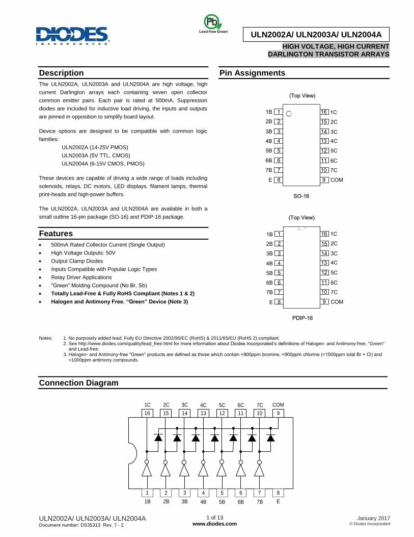
Pin Assignments
1
2
3
4
5
6
7
8
16
15
14
13
12
11
10
9
1B
2B
3B
4B
5B
6B
7B
E
1C
2C
3C
4C
5C
6C
7C
COM
(Top View)
SO-16
1
2
3
4
5
6
7
8
16
15
14
13
12
11
10
9
1B
2B
3B
4B
5B
6B
7B
E
1C
2C
3C
4C
5C
6C
7C
COM
(Top View)
PDIP-16
Notes: 1. No purposely added lead. Fully EU Directive 2002/95/EC (RoHS) & 2011/65/EU (RoHS 2) compliant. 2. See http://www.diodes.com/quality/lead_free.html for more information about Diodes Incorporated’s definitions of Halogen- and Antimony-free, "Green" and Lead-free. 3. Halogen- and Antimony-free "Green‖ products are defined as those which contain <900ppm bromine, <900ppm chlorine (<1500ppm total Br + Cl) and <1000ppm antimony compounds.
Connection Diagram
910111213141516
1 2 3 4 5 6 7 8
1C 2C 3C 4C 5C 6C 7C COM
1B 2B 3B 4B 5B 6B 7B E
ULN2002A/ ULN2003A/ ULN2004A Document number: DS35313 Rev. 7 - 2
2 of 13 www.diodes.com
January 2017 © Diodes Incorporated
ULN2002A/ ULN2003A/ ULN2004A ULN2004A
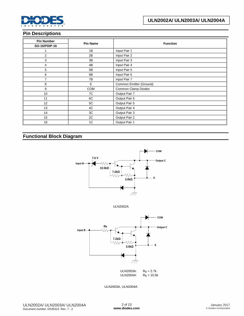
Pin Descriptions
Pin Number Pin Name Function
SO-16/PDIP-16
1 1B Input Pair 1
2 2B Input Pair 2
3 3B Input Pair 3
4 4B Input Pair 4
5 5B Input Pair 5
6 6B Input Pair 6
7 7B Input Pair 7
8 E Common Emitter (Ground)
9 COM Common Clamp Diodes
10 7C Output Pair 7
11 6C Output Pair 6
12 5C Output Pair 5
13 4C Output Pair 4
14 3C Output Pair 3
15 2C Output Pair 2
16 1C Output Pair 1
Functional Block Diagram
COM
Output C
7.2kΩ
3.0kΩ
10.5kΩ
7.0 V
Input B
E
ULN2002A
COM
Output C
7.2kΩ
3.0kΩ
RB
Input B
E
ULN2003A: RB = 2.7k
ULN2004A: RB = 10.5k
ULN2003A, ULN2004A
ULN2002A/ ULN2003A/ ULN2004A Document number: DS35313 Rev. 7 - 2
3 of 13 www.diodes.com
January 2017 © Diodes Incorporated
ULN2002A/ ULN2003A/ ULN2004A ULN2004A
Absolute Maximum Ratings (Note 4) (@TA = +25°C, unless otherwise specified.)
Symbol Parameter Rating Unit
VCC Collector to Emitter Voltage 50 V
VR Clamp Diode Reverse Voltage (Note 5) 50 V
VI Input Voltage (Note 5) 30 V
ICP Peak Collector Current 500 mA
IOK Output Clamp Current 500 mA
ITE Total Emitter Current -2.5 A
θJA Thermal Resistance Junction-to-Ambient (Note 6) SO-16 63.0
°C/W PDIP-16 50.0
θJC Thermal Resistance Junction-to-Case (Note 7) SO-16 12.0
°C/W PDIP-16 15.0
TJ Junction Temperature +150 °C
TSTG Storage Temperature -65 to +150 °C
Notes: 4. Stresses beyond those listed under "absolute maximum ratings" may cause permanent damage to the device. These are stress ratings only. Functional operation of the device at these or any other conditions beyond those indicated under "recommended operating conditions" is not implied. Exposure to absolute-maximum-rated conditions for extended periods may affect device reliability.
5. All voltage values are with respect to the emitter/substrate terminal E, unless otherwise noted.
6. Maximum power dissipation is a function of TJ(max), θJA and TA. The maximum allowable power dissipation at any allowable ambient temperature
is PD = (TJ(max) – TA)/θJA. Operating at the absolute maximum TJ of +150°C can affect reliability.
7. Maximum power dissipation is a function of TJ(max), θJC and TA. The maximum allowable power dissipation at any allowable ambient temperature
is PD = (TJ(max) – TC)/θJC. Operating at the absolute maximum TJ of +150°C can affect reliability.
Recommended Operating Conditions
Symbol Parameter Min Max Unit
VCC Collector to Emitter Voltage — 50 V
TA Operating Ambient Temperature -40 +105 °C
Electrical Characteristics (@TA = +25°C, unless otherwise specified.)
ULN2002A
Symbol Parameter Test Figure Test Conditions Min Typ Max Unit
VI(ON) On State Input Voltage 6 VCE = 2V, IC = 300mA — — 13 V
VCE(SAT) Collector Emitter Saturation Voltage
5
II = 250µA, IC = 100mA — 0.9 1.1
V II = 350µA, IC = 200mA — 1 1.3
II = 500µA, IC = 350mA — 1.2 1.6
VF Clamp Forward Voltage 8 IF = 350mA — 1.7 2 V
ICEX Collector Cut-off Current
1 VCE = 50V, II = 0 — — 50
µA 2
VCE = 50V,
TA = +105°C
II = 0 — — 100
VI = 6V — — 500
II(OFF) Off State Input Current 3 VCE = 50V, IC = 500µA 50 65 — µA
II Input Current 4 VI = 17V — 0.82 1.25 mA
IR Clamp Reverse Current 7 VR = 50V TA = +105°C — — 100
µA — — — 50
CI Input Capacitance — VI = 0, f = 1MHz — — 25 pF
ULN2002A/ ULN2003A/ ULN2004A Document number: DS35313 Rev. 7 - 2
4 of 13 www.diodes.com
January 2017 © Diodes Incorporated
ULN2002A/ ULN2003A/ ULN2004A ULN2004A
Electrical Characteristics (Cont.) (@TA = +25°C, unless otherwise specified.)
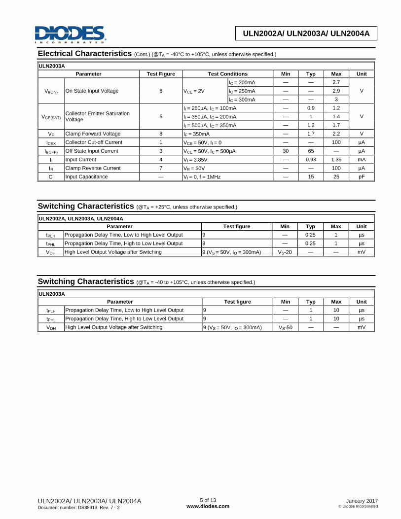
ULN2003A
Parameter Test Figure Test Conditions Min Typ Max Unit
VI(ON) On State Input Voltage 6 VCE = 2V
IC = 200mA — — 2.4
V IC = 250mA — — 2.7
IC = 300mA — — 3
VCE(SAT) Collector Emitter Saturation Voltage
5
II = 250µA, IC = 100mA — 0.9 1.1
V II = 350µA, IC = 200mA — 1 1.3
II = 500µA, IC = 350mA — 1.2 1.6
VF Clamp Forward Voltage 8 IF = 350mA — 1.7 2 V
ICEX Collector Cut-off Current
1 VCE = 50V, II = 0 — — 50
µA 2
VCE = 50V,
TA = +105°C II = 0 — — 100
II(OFF) Off State Input Current 3 VCE = 50V, IC = 500µA 50 65 — µA
II Input Current 4 VI = 3.85V — 0.93 1.35 mA
IR Clamp Reverse Current 7 VR = 50V TA = +105°C — — 100
µA — — — 50
CI Input Capacitance — VI = 0, f = 1MHz — 15 25 pF
ULN2004A
Parameter Test Figure Test Conditions Min Typ Max Unit
VI(ON) On State Input Voltage 6 VCE = 2V
IC = 125mA — — 5
V IC = 200mA — — 6
IC = 275mA — — 7
IC = 350mA — — 8
VCE(SAT) Collector Emitter Saturation Voltage
5
II = 250µA, IC = 100mA — 0.9 1.1
V II = 350µA, IC = 200mA — 1 1.3
II = 500µA, IC = 350mA — 1.2 1.6
VF Clamp Forward Voltage 8 IF = 350mA — 1.7 2 V
ICEX Collector Cut-off Current
1 VCE = 50V, II = 0 — — 50
µA 2 VCE = 50V, TA = +105°C
II = 0 — — 100
VI = 6V — — 500
II(OFF) Off State Input Current 3 VCE = 50V, IC = 500µA 50 65 — µA
II Input Current 4 VI = 5V — 0.35 0.5 mA
IR Clamp Reverse Current 7 VR = 50V TA = +105°C — — 100
µA — — — 50
CI Input Capacitance — VI = 0, f = 1MHz — 15 25 pF
ULN2002A/ ULN2003A/ ULN2004A Document number: DS35313 Rev. 7 - 2
5 of 13 www.diodes.com
January 2017 © Diodes Incorporated
ULN2002A/ ULN2003A/ ULN2004A ULN2004A
Electrical Characteristics (Cont.) (@TA = -40°C to +105°C, unless otherwise specified.)
ULN2003A
Parameter Test Figure Test Conditions Min Typ Max Unit
VI(ON) On State Input Voltage 6 VCE = 2V
IC = 200mA — — 2.7
V IC = 250mA — — 2.9
IC = 300mA — — 3
VCE(SAT) Collector Emitter Saturation Voltage
5
II = 250µA, IC = 100mA — 0.9 1.2
V II = 350µA, IC = 200mA — 1 1.4
II = 500µA, IC = 350mA — 1.2 1.7
VF Clamp Forward Voltage 8 IF = 350mA — 1.7 2.2 V
ICEX Collector Cut-off Current 1 VCE = 50V, II = 0 — — 100 µA
II(OFF) Off State Input Current 3 VCE = 50V, IC = 500µA 30 65 — µA
II Input Current 4 VI = 3.85V — 0.93 1.35 mA
IR Clamp Reverse Current 7 VR = 50V — — 100 µA
CI Input Capacitance — VI = 0, f = 1MHz — 15 25 pF
Switching Characteristics (@TA = +25°C, unless otherwise specified.)
ULN2002A, ULN2003A, ULN2004A
Parameter Test figure Min Typ Max Unit
tPLH Propagation Delay Time, Low to High Level Output 9 — 0.25 1 µs
tPHL Propagation Delay Time, High to Low Level Output 9 — 0.25 1 µs
VOH High Level Output Voltage after Switching 9 (VS = 50V, IO = 300mA) VS-20 — — mV
Switching Characteristics (@TA = -40 to +105°C, unless otherwise specified.)
ULN2003A
Parameter Test figure Min Typ Max Unit
tPLH Propagation Delay Time, Low to High Level Output 9 — 1 10 µs
tPHL Propagation Delay Time, High to Low Level Output 9 — 1 10 µs
VOH High Level Output Voltage after Switching 9 (VS = 50V, IO = 300mA) VS-50 — — mV
ULN2002A/ ULN2003A/ ULN2004A Document number: DS35313 Rev. 7 - 2
6 of 13 www.diodes.com
January 2017 © Diodes Incorporated
ULN2002A/ ULN2003A/ ULN2004A ULN2004A
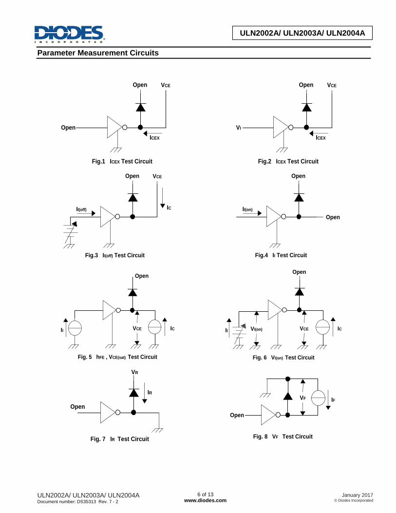
Parameter Measurement Circuits
VCEOpen
Open
ICEX
Fig.1 ICEX Test Circuit
Open
VI
ICEX
VCE
Fig.2 ICEX Test Circuit
Open
II(off) IC
VCE
Fig.3 II(off) Test Circuit
Open
II(on)
Fig.4 II Test Circuit
Open
Open
II ICVCE
Fig. 5 hFE , VCE(sat) Test Circuit
Open
II ICVCE
Fig. 6 VI(on) Test Circuit
VI(on)
IR
Open
Fig. 7 IR Test Circuit
VR
VF
Open
IF
Fig. 8 VF Test Circuit
ULN2002A/ ULN2003A/ ULN2004A Document number: DS35313 Rev. 7 - 2
7 of 13 www.diodes.com
January 2017 © Diodes Incorporated
ULN2002A/ ULN2003A/ ULN2004A ULN2004A
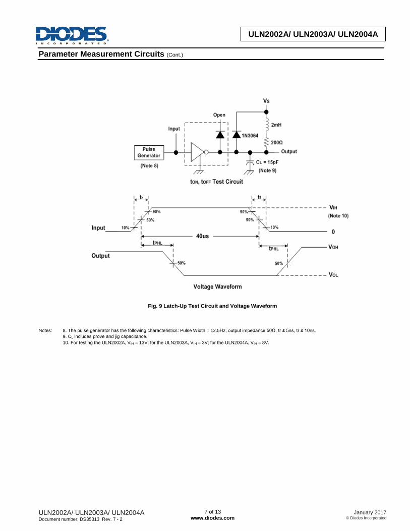
Parameter Measurement Circuits (Cont.)
Fig. 9 Latch-Up Test Circuit and Voltage Waveform Notes: 8. The pulse generator has the following characteristics: Pulse Width = 12.5Hz, output impedance 50Ω, tr ≤ 5ns, tr ≤ 10ns.
9. CL includes prove and jig capacitance.
10. For testing the ULN2002A, VIH = 13V; for the ULN2003A, VIH = 3V; for the ULN2004A, VIH = 8V.
ULN2002A/ ULN2003A/ ULN2004A Document number: DS35313 Rev. 7 - 2
8 of 13 www.diodes.com
January 2017 © Diodes Incorporated
ULN2002A/ ULN2003A/ ULN2004A ULN2004A
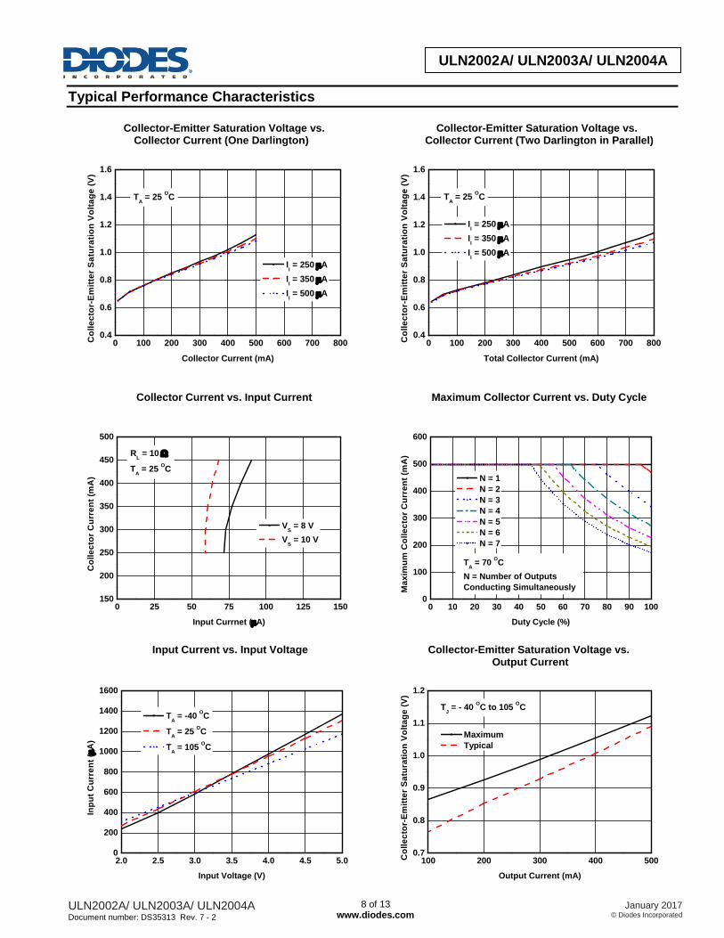
Typical Performance Characteristics
Collector-Emitter Saturation Voltage vs. Collector Current (One Darlington)
0 100 200 300 400 500 600 700 8000.4
0.6
0.8
1.0
1.2
1.4
1.6
TA = 25
OC
Co
lle
cto
r-E
mit
ter
Sa
tura
tio
n V
olt
ag
e (
V)
Collector Current (mA)
II = 250 A
II = 350 A
II = 500 A
Collector Current vs. Input Current
Collector-Emitter Saturation Voltage vs. Collector Current (Two Darlington in Parallel)
0 100 200 300 400 500 600 700 8000.4
0.6
0.8
1.0
1.2
1.4
1.6
Co
lle
cto
r-E
mit
ter
Sa
tura
tio
n V
olt
ag
e (
V)
Total Collector Current (mA)
II = 250 A
II = 350 A
II = 500 A
TA = 25
OC
Maximum Collector Current vs. Duty Cycle
0 25 50 75 100 125 150150
200
250
300
350
400
450
500
Co
lle
cto
r C
urr
en
t (m
A)
Input Currnet (A)
VS = 8 V
VS = 10 V
RL = 10
TA = 25
OC
Input Current vs. Input Voltage
0 10 20 30 40 50 60 70 80 90 1000
100
200
300
400
500
600
Ma
xim
um
Co
lle
cto
r C
urr
en
t (m
A)
Duty Cycle (%)
N = 1
N = 2
N = 3
N = 4
N = 5
N = 6
N = 7
TA = 70
OC
N = Number of Outputs
Conducting Simultaneously
Collector-Emitter Saturation Voltage vs.
Output Current
2.0 2.5 3.0 3.5 4.0 4.5 5.00
200
400
600
800
1000
1200
1400
1600
Inp
ut
Cu
rre
nt
(A
)
Input Voltage (V)
TA = -40
OC
TA = 25
OC
TA = 105
OC
100 200 300 400 5000.7
0.8
0.9
1.0
1.1
1.2
Co
lle
cto
r-E
mit
ter
Sa
tura
tio
n V
olt
ag
e (
V)
Output Current (mA)
Maximum
Typical
TJ = - 40
OC to 105
OC

ULN2002A/ ULN2003A/ ULN2004A Document number: DS35313 Rev. 7 - 2
9 of 13 www.diodes.com
January 2017 © Diodes Incorporated
ULN2002A/ ULN2003A/ ULN2004A ULN2004A
Typical Performance Characteristics (Cont.)
Output Current vs. Input Current
50 55 60 65 70 75 80 85100
150
200
250
300
350
400
450
500
Ou
tpu
t C
urr
en
t (m
A)
Input Current (A)
Minimum
VCE
= 2 V
TJ = - 40
OC to 105
OC
ULN2002A/ ULN2003A/ ULN2004A Document number: DS35313 Rev. 7 - 2
10 of 13 www.diodes.com
January 2017 © Diodes Incorporated
ULN2002A/ ULN2003A/ ULN2004A ULN2004A
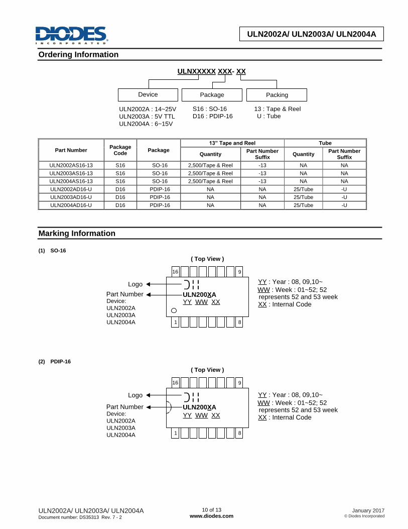
Ordering Information
ULNXXXXX XXX- XX
Packing
13 : Tape & Reel
Package
S16 : SO-16
D16 : PDIP-16
Device
ULN2002A : 14~25V
ULN2003A : 5V TTL
ULN2004A : 6~15V
U : Tube
Part Number Package
Code Package
13” Tape and Reel Tube
Quantity Part Number
Suffix Quantity
Part Number Suffix
ULN2002AS16-13 S16 SO-16 2,500/Tape & Reel -13 NA NA
ULN2003AS16-13 S16 SO-16 2,500/Tape & Reel -13 NA NA
ULN2004AS16-13 S16 SO-16 2,500/Tape & Reel -13 NA NA
ULN2002AD16-U D16 PDIP-16 NA NA 25/Tube -U
ULN2003AD16-U D16 PDIP-16 NA NA 25/Tube -U
ULN2004AD16-U D16 PDIP-16 NA NA 25/Tube -U
Marking Information
(1) SO-16
( Top View )
1
9
8
ULN200XA
Logo
16
Part NumberWW : Week : 01~52; 52
YY : Year : 08, 09,10~
XX : Internal Coderepresents 52 and 53 week
YY WW XXDevice:
ULN2002A
ULN2003A
ULN2004A
(2) PDIP-16
( Top View )
1
9
8
ULN200XA
Logo
16
Part NumberWW : Week : 01~52; 52
YY : Year : 08, 09,10~
XX : Internal Coderepresents 52 and 53 week
YY WW XXDevice:
ULN2002A
ULN2003A
ULN2004A
ULN2002A/ ULN2003A/ ULN2004A Document number: DS35313 Rev. 7 - 2
11 of 13 www.diodes.com
January 2017 © Diodes Incorporated
ULN2002A/ ULN2003A/ ULN2004A ULN2004A
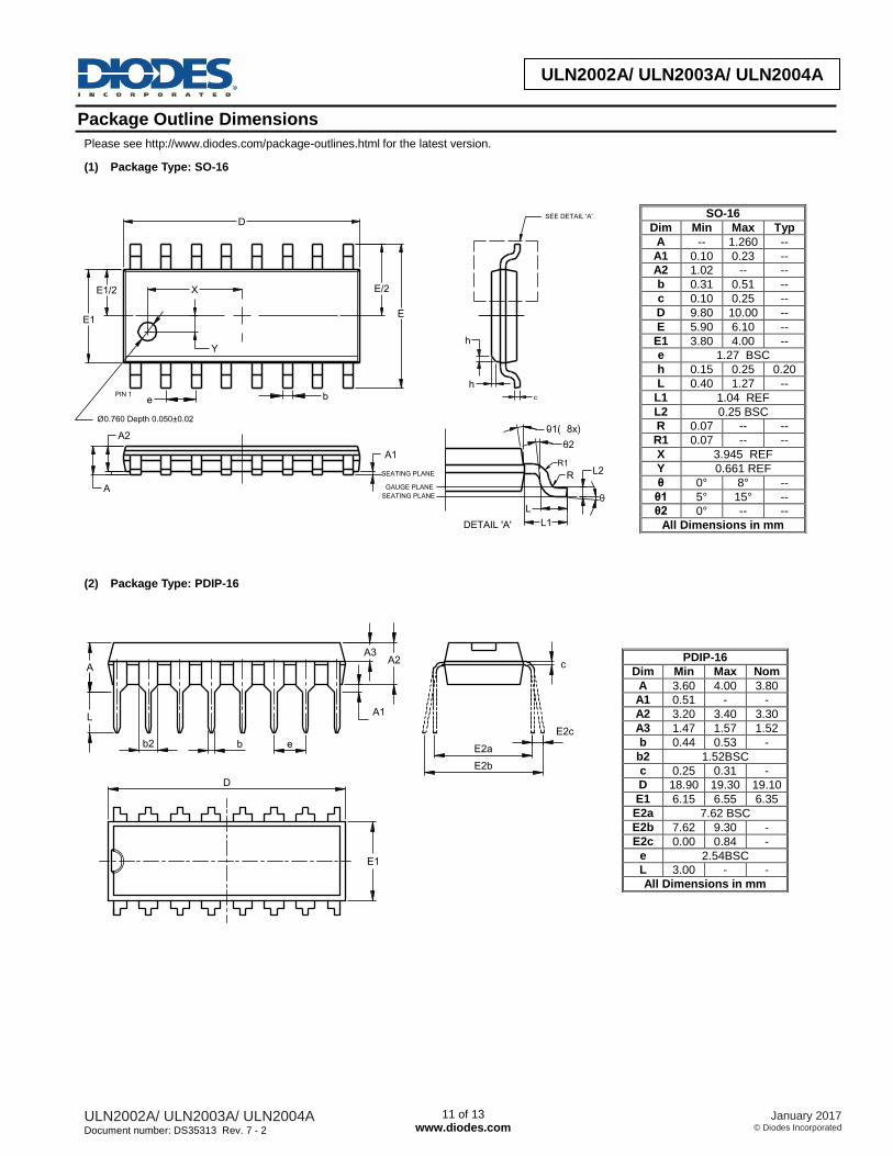
Package Outline Dimensions
Please see http://www.diodes.com/package-outlines.html for the latest version.
(1) Package Type: SO-16
(2) Package Type: PDIP-16
A2A
LA1
b2 b
E1
D
c
e
E2b
A3
E2a
E2c
SO-16
Dim Min Max Typ
A -- 1.260 --
A1 0.10 0.23 --
A2 1.02 -- --
b 0.31 0.51 --
c 0.10 0.25 --
D 9.80 10.00 --
E 5.90 6.10 --
E1 3.80 4.00 --
e 1.27 BSC
h 0.15 0.25 0.20
L 0.40 1.27 --
L1 1.04 REF
L2 0.25 BSC
R 0.07 -- --
R1 0.07 -- --
X 3.945 REF
Y 0.661 REF
θ 0° 8° --
θ1 5° 15° --
θ2 0° -- --
All Dimensions in mm
PDIP-16
Dim Min Max Nom
A 3.60 4.00 3.80
A1 0.51 - -
A2 3.20 3.40 3.30
A3 1.47 1.57 1.52
b 0.44 0.53 -
b2 1.52BSC
c 0.25 0.31 -
D 18.90 19.30 19.10
E1 6.15 6.55 6.35
E2a 7.62 BSC
E2b 7.62 9.30 -
E2c 0.00 0.84 -
e 2.54BSC
L 3.00 - -
All Dimensions in mm
PIN 1
SEE DETAIL 'A'
A1
e b
E
E/2
E1
E1/2
D
SEATING PLANE
A2
A GAUGE PLANE
0
R1
R
02
L
L1
L2
Ø 0.760 Depth 0.050± 0.02
h
h
X
Y
01(8x)
DETAIL 'A'
SEATING PLANE
c
ULN2002A/ ULN2003A/ ULN2004A Document number: DS35313 Rev. 7 - 2
12 of 13 www.diodes.com
January 2017 © Diodes Incorporated
ULN2002A/ ULN2003A/ ULN2004A ULN2004A
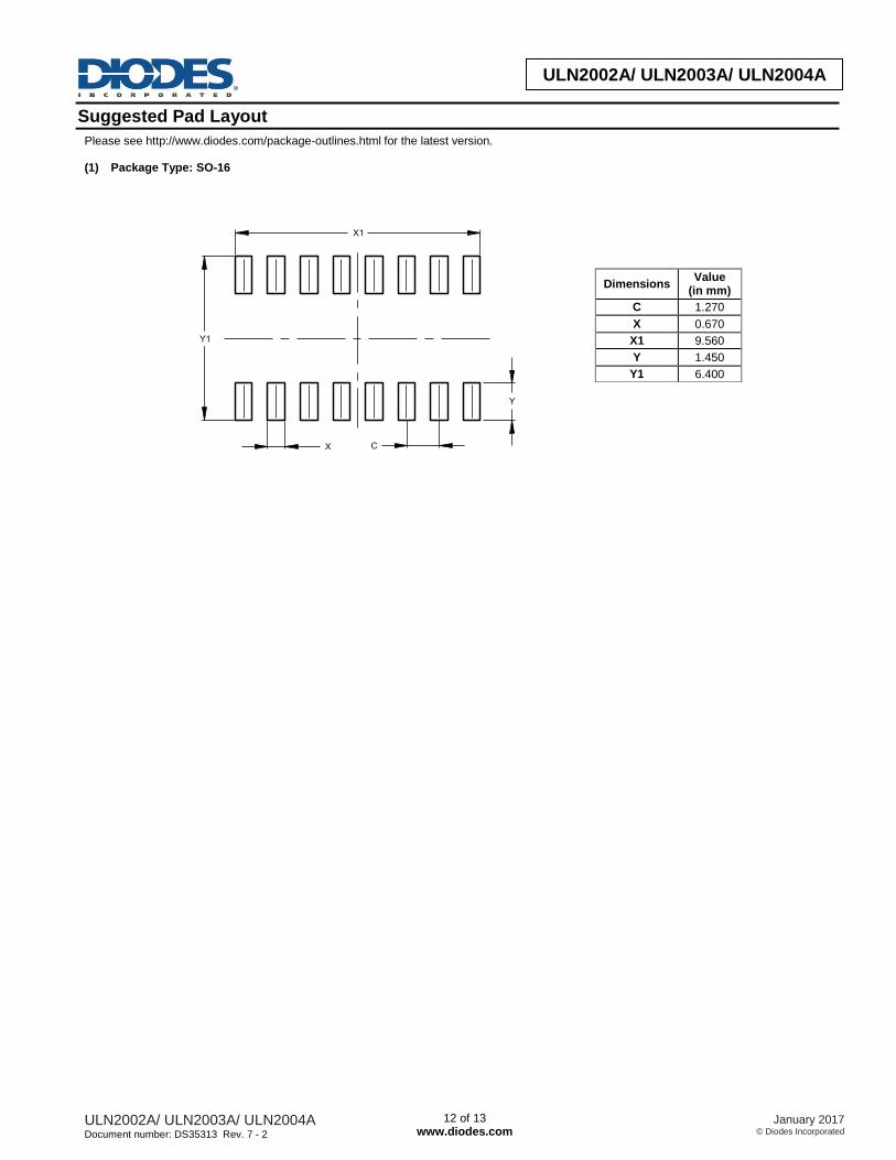
Suggested Pad Layout
Please see http://www.diodes.com/package-outlines.html for the latest version.
(1) Package Type: SO-16
Dimensions Value
(in mm)
C 1.270
X 0.670
X1 9.560
Y 1.450
Y1 6.400
X1
X C
Y

ULN2002A/ ULN2003A/ ULN2004A Document number: DS35313 Rev. 7 - 2
13 of 13 www.diodes.com
January 2017 © Diodes Incorporated
ULN2002A/ ULN2003A/ ULN2004A ULN2004A
IMPORTANT NOTICE DIODES INCORPORATED MAKES NO WARRANTY OF ANY KIND, EXPRESS OR IMPLIED, WITH REGARDS TO THIS DOCUMENT, INCLUDING, BUT NOT LIMITED TO, THE IMPLIED WARRANTIES OF MERCHANTABILITY AND FITNESS FOR A PARTICULAR PURPOSE (AND THEIR EQUIVALENTS UNDER THE LAWS OF ANY JURISDICTION). Diodes Incorporated and its subsidiaries reserve the right to make modifications, enhancements, improvements, corrections or other changes without further notice to this document and any product described herein. Diodes Incorporated does not assume any liability arising out of the application or use of this document or any product described herein; neither does Diodes Incorporated convey any license under its patent or trademark rights, nor the rights of others. Any Customer or user of this document or products described herein in such applications shall assume all risks of such use and will agree to hold Diodes Incorporated and all the companies whose products are represented on Diodes Incorporated website, harmless against all damages. Diodes Incorporated does not warrant or accept any liability whatsoever in respect of any products purchased through unauthorized sales channel. Should Customers purchase or use Diodes Incorporated products for any unintended or unauthorized application, Customers shall indemnify and hold Diodes Incorporated and its representatives harmless against all claims, damages, expenses, and attorney fees arising out of, directly or indirectly, any claim of personal injury or death associated with such unintended or unauthorized application. Products described herein may be covered by one or more United States, international or foreign patents pending. Product names and markings noted herein may also be covered by one or more United States, international or foreign trademarks. This document is written in English but may be translated into multiple languages for reference. Only the English version of this document is the final and determinative format released by Diodes Incorporated.
LIFE SUPPORT Diodes Incorporated products are specifically not authorized for use as critical components in life support devices or systems without the express written approval of the Chief Executive Officer of Diodes Incorporated. As used herein: A. Life support devices or systems are devices or systems which: 1. are intended to implant into the body, or
2. support or sustain life and whose failure to perform when properly used in accordance with instructions for use provided in the labeling can be reasonably expected to result in significant injury to the user.
B. A critical component is any component in a life support device or system whose failure to perform can be reasonably expected to cause the failure of the life support device or to affect its safety or effectiveness. Customers represent that they have all necessary expertise in the safety and regulatory ramifications of their life support devices or systems, and acknowledge and agree that they are solely responsible for all legal, regulatory and safety-related requirements concerning their products and any use of Diodes Incorporated products in such safety-critical, life support devices or systems, notwithstanding any devices- or systems-related information or support that may be provided by Diodes Incorporated. Further, Customers must fully indemnify Diodes Incorporated and its representatives against any damages arising out of the use of Diodes Incorporated products in such safety-critical, life support devices or systems. Copyright © 2017, Diodes Incorporated www.diodes.com