78k0/kc2 8-bit single-chip microcontrollers um · 6 user’s manual u17336ej5v0ud introduction...
TRANSCRIPT

Document No. U17336EJ5V0UD00 (5th edition)
Date Published February 2007 N CP(K)
Printed in Japan 2005
μPD78F0511 μPD78F0511(A) μPD78F0511(A2) μPD78F0512 μPD78F0512(A) μPD78F0512(A2) μPD78F0513 μPD78F0513(A) μPD78F0513(A2) μPD78F0514 μPD78F0514(A) μPD78F0514(A2) μPD78F0515 μPD78F0515(A) μPD78F0515(A2) μPD78F0513D μPD78F0515D
78K0/KC2 8-bit Single-Chip Microcontrollers
User’s Manual
The μPD78F0513D and 78F0515D have on-chip debug functions.
Do not use these products for mass production because its reliability cannot be guaranteed after the on-chip debug
function has been used, due to issues with respect to the number of times the flash memory can be rewritten. NEC
Electronics does not accept complaints concerning these products.

User’s Manual U17336EJ5V0UD 2
[MEMO]

User’s Manual U17336EJ5V0UD 3
1
2
3
4
VOLTAGE APPLICATION WAVEFORM AT INPUT PIN
Waveform distortion due to input noise or a reflected wave may cause malfunction. If the input of the

User’s Manual U17336EJ5V0UD 4
EEPROM is a trademark of NEC Electronics Corporation.
Windows and Windows NT are registered trademarks or trademarks of Microsoft Corporation in the United
States and/or other countries.
PC/AT is a trademark of International Business Machines Corporation.
HP9000 series 700 and HP-UX are trademarks of Hewlett-Packard Company.
SPARCstation is a trademark of SPARC International, Inc.
Solaris and SunOS are trademarks of Sun Microsystems, Inc.
SuperFlash is a registered trademark of Silicon Storage Technology, Inc. in several countries including the
United States and Japan.

User’s Manual U17336EJ5V0UD 5
Caution: This product uses SuperFlash® technology licensed from Silicon Storage Technology, Inc.

User’s Manual U17336EJ5V0UD 6
INTRODUCTION
Readers This manual is intended for user engineers who wish to understand the functions of the
78K0/KC2 and design and develop application systems and programs for these devices.
The target products are as follows.
78K0/KC2: μPD78F0511, 78F0512, 78F0513, 78F0514, 78F0515, 78F0513D,
78F0515D, 78F0511(A), 78F0512(A), 78F0513(A), 78F0514(A),
78F0515(A), 78F0511(A2), 78F0512(A2), 78F0513(A2), 78F0514(A2),
78F0515(A2)
Purpose This manual is intended to give users an understanding of the functions described in the
Organization below.
Organization The 78K0/KC2 manual is separated into two parts: this manual and the instructions
edition (common to 78K0 microcontrollers).
78K0/KC2
User’s Manual
(This Manual)
78K/0 Series
User’s Manual
Instructions
• Pin functions
• Internal block functions
• Interrupts
• Other on-chip peripheral functions
• Electrical specifications
• CPU functions
• Instruction set
• Explanation of each instruction
How to Read This Manual It is assumed that the readers of this manual have general knowledge of electrical
engineering, logic circuits, and microcontrollers.
• When using this manual as the manual for (A) grade products and (A2) grade
products:
→ Only the quality grade differs between standard products, (A) grade products, and
(A2) grade products. Read the part number as follows.
• μPD78F0511→ μPD78F0511(A), 78F0511(A2)
• μPD78F0512→ μPD78F0512(A), 78F0512(A2)
• μPD78F0513→ μPD78F0513(A), 78F0513(A2)
• μPD78F0514→ μPD78F0514(A), 78F0514(A2)
• μPD78F0515→ μPD78F0515(A), 78F0515(A2)
• To gain a general understanding of functions:
→ Read this manual in the order of the CONTENTS. The mark “<R>” shows major
revised points. The revised points can be easily searched by copying an “<R>” in
the PDF file and specifying it in the “Find what:” field.
• How to interpret the register format:
→ For a bit number enclosed in angle brackets, the bit name is defined as a
reserved word in the RA78K0, and is defined as an sfr variable using the
#pragma sfr directive in the CC78K0.
<R>
<R>
<R>

User’s Manual U17336EJ5V0UD 7
• To check the details of a register when you know the register name:
→ See APPENDIX C REGISTER INDEX.
• To know details of the 78K0 microcontroller instructions:
→ Refer to the separate document 78K/0 Series Instructions User’s Manual
(U12326E).
Conventions Data significance: Higher digits on the left and lower digits on the right
Active low representations: ××× (overscore over pin and signal name)
Note: Footnote for item marked with Note in the text
Caution: Information requiring particular attention
Remark: Supplementary information
Numerical representations: Binary ... ×××× or ××××B
Decimal ... ××××
Hexadecimal ... ××××H
Related Documents The related documents indicated in this publication may include preliminary versions.
However, preliminary versions are not marked as such.
Documents Related to Devices
Document Name Document No.
78K0/KC2 User’s Manual This manual
78K/0 Series Instructions User’s Manual U12326E
78K0/Kx2 Flash Memory Programming (Programmer) Application Note U17739E
78K0/Kx2 Flash Memory Self Programming User’s ManualNote U17516E
78K0/Kx2 EEPROMTM Emulation Application NoteNote U17517E
Note This document is under engineering management. For details, consult an NEC Electronics sales
representative.
Documents Related to Development Tools (Software) (User’s Manuals)
Document Name Document No.
Operation U17199E
Language U17198E
RA78K0 Ver. 3.80 Assembler Package
Structured Assembly Language U17197E
Operation U17201E CC78K0 Ver. 3.70 C Compiler
Language U17200E
Operation U17246E SM+ System Simulator
User Open Interface U17247E
ID78K0-QB Ver. 2.90 Integrated Debugger Operation U17437E
PM plus Ver. 5.20 U16934E
Caution The related documents listed above are subject to change without notice. Be sure to use the latest
version of each document when designing.
<R>
User’s Manual U17336EJ5V0UD 8
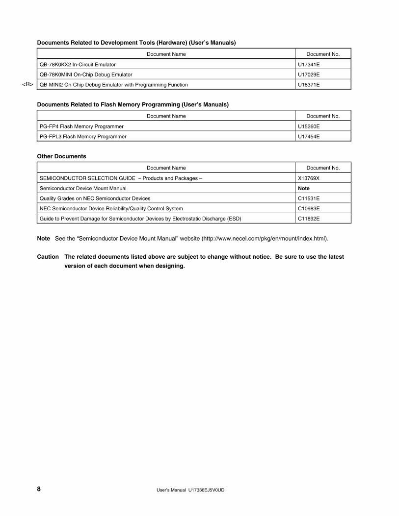
Documents Related to Development Tools (Hardware) (User’s Manuals)
Document Name Document No.
QB-78K0KX2 In-Circuit Emulator U17341E
QB-78K0MINI On-Chip Debug Emulator U17029E
QB-MINI2 On-Chip Debug Emulator with Programming Function U18371E
Documents Related to Flash Memory Programming (User’s Manuals)
Document Name Document No.
PG-FP4 Flash Memory Programmer U15260E
PG-FPL3 Flash Memory Programmer U17454E
Other Documents
Document Name Document No.
SEMICONDUCTOR SELECTION GUIDE − Products and Packages − X13769X
Semiconductor Device Mount Manual Note
Quality Grades on NEC Semiconductor Devices C11531E
NEC Semiconductor Device Reliability/Quality Control System C10983E
Guide to Prevent Damage for Semiconductor Devices by Electrostatic Discharge (ESD) C11892E
Note See the “Semiconductor Device Mount Manual” website (http://www.necel.com/pkg/en/mount/index.html).
Caution The related documents listed above are subject to change without notice. Be sure to use the latest
version of each document when designing.
<R>

User’s Manual U17336EJ5V0UD 9
CONTENTS
CHAPTER 1 OUTLINE ............................................................................................................................ 17
1.1 Features .................................................................................................................................... 17 1.2 Applications ............................................................................................................................. 18 1.3 Ordering Information ............................................................................................................... 19 1.4 Pin Configuration (Top View).................................................................................................. 20 1.5 78K0/Kx2 Microcontroller Lineup........................................................................................... 26 1.6 Block Diagram.......................................................................................................................... 29 1.7 Outline of Functions ................................................................................................................ 30
CHAPTER 2 PIN FUNCTIONS............................................................................................................... 33
2.1 Pin Function List...................................................................................................................... 33 2.2 Description of Pin Functions.................................................................................................. 36
2.2.1 P00 and P01 (port 0)..................................................................................................................36 2.2.2 P10 to P17 (port 1).....................................................................................................................37 2.2.3 P20 to P27 (port 2).....................................................................................................................38 2.2.4 P30 to P33 (port 3).....................................................................................................................38 2.2.5 P40 and P41 (port 4) (44-pin and 48-pin products only) ............................................................39 2.2.6 P60 to P63 (port 6).....................................................................................................................39 2.2.7 P70 to P75 (port 7).....................................................................................................................40 2.2.8 P120 to P124 (port 12)...............................................................................................................40 2.2.9 P130 (port 13) (48-pin products only).........................................................................................41 2.2.10 P140 (port 14) (48-pin products only).........................................................................................41 2.2.11 AVREF ........................................................................................................................................42 2.2.12 AVSS ..........................................................................................................................................42 2.2.13 RESET.......................................................................................................................................42 2.2.14 REGC.........................................................................................................................................42 2.2.15 VDD ............................................................................................................................................42 2.2.16 VSS ............................................................................................................................................42 2.2.17 FLMD0 .......................................................................................................................................42
2.3 Pin I/O Circuits and Recommended Connection of Unused Pins....................................... 43
CHAPTER 3 CPU ARCHITECTURE...................................................................................................... 47
3.1 Memory Space.......................................................................................................................... 47 3.1.1 Internal program memory space ................................................................................................56 3.1.2 Internal data memory space.......................................................................................................58 3.1.3 Special function register (SFR) area ..........................................................................................59 3.1.4 Data memory addressing ...........................................................................................................59
3.2 Processor Registers ................................................................................................................ 65 3.2.1 Control registers.........................................................................................................................65 3.2.2 General-purpose registers .........................................................................................................69 3.2.3 Special function registers (SFRs)...............................................................................................70
3.3 Instruction Address Addressing ............................................................................................ 75 3.3.1 Relative addressing....................................................................................................................75

User’s Manual U17336EJ5V0UD 10
3.3.2 Immediate addressing ............................................................................................................... 76 3.3.3 Table indirect addressing .......................................................................................................... 77 3.3.4 Register addressing .................................................................................................................. 77
3.4 Operand Address Addressing ................................................................................................ 78 3.4.1 Implied addressing .................................................................................................................... 78 3.4.2 Register addressing .................................................................................................................. 79 3.4.3 Direct addressing ...................................................................................................................... 80 3.4.4 Short direct addressing ............................................................................................................. 81 3.4.5 Special function register (SFR) addressing ............................................................................... 82 3.4.6 Register indirect addressing...................................................................................................... 83 3.4.7 Based addressing...................................................................................................................... 84 3.4.8 Based indexed addressing ........................................................................................................ 85 3.4.9 Stack addressing....................................................................................................................... 86
CHAPTER 4 PORT FUNCTIONS ........................................................................................................... 87
4.1 Port Functions.......................................................................................................................... 87 4.2 Port Configuration ................................................................................................................... 89
4.2.1 Port 0......................................................................................................................................... 90 4.2.2 Port 1......................................................................................................................................... 92 4.2.3 Port 2......................................................................................................................................... 97 4.2.4 Port 3......................................................................................................................................... 99 4.2.5 Port 4 (44-pin and 48-pin products only) ..................................................................................102 4.2.6 Port 6........................................................................................................................................103 4.2.7 Port 7........................................................................................................................................105 4.2.8 Port 12......................................................................................................................................106 4.2.9 Port 13 (48-pin products only) ..................................................................................................109 4.2.10 Port 14 (48-pin products only) ..................................................................................................110
4.3 Registers Controlling Port Function .................................................................................... 111 4.4 Port Function Operations...................................................................................................... 116
4.4.1 Writing to I/O port .....................................................................................................................116 4.4.2 Reading from I/O port...............................................................................................................116 4.4.3 Operations on I/O port..............................................................................................................116
4.5 Settings of Port Mode Register and Output Latch When Using Alternate Function....... 117 4.6 Cautions on 1-bit Manipulation Instruction for Port Register n (Pn) ................................ 119
CHAPTER 5 CLOCK GENERATOR .................................................................................................... 120
5.1 Functions of Clock Generator............................................................................................... 120 5.2 Configuration of Clock Generator ........................................................................................ 121 5.3 Registers Controlling Clock Generator ............................................................................... 123 5.4 System Clock Oscillator ........................................................................................................ 132
5.4.1 X1 oscillator..............................................................................................................................132 5.4.2 XT1 oscillator ...........................................................................................................................132 5.4.3 When subsystem clock is not used ..........................................................................................135 5.4.4 Internal high-speed oscillator ...................................................................................................135 5.4.5 Internal low-speed oscillator.....................................................................................................135 5.4.6 Prescaler ..................................................................................................................................135
5.5 Clock Generator Operation ................................................................................................... 136 5.6 Controlling Clock ................................................................................................................... 140

User’s Manual U17336EJ5V0UD 11
5.6.1 Controlling high-speed system clock........................................................................................140 5.6.2 Example of controlling internal high-speed oscillation clock.....................................................143 5.6.3 Example of controlling subsystem clock...................................................................................145 5.6.4 Example of controlling internal low-speed oscillation clock ......................................................147 5.6.5 Clocks supplied to CPU and peripheral hardware....................................................................147 5.6.6 CPU clock status transition diagram ........................................................................................148 5.6.7 Condition before changing CPU clock and processing after changing CPU clock ...................153 5.6.8 Time required for switchover of CPU clock and main system clock .........................................154 5.6.9 Conditions before clock oscillation is stopped..........................................................................155 5.6.10 Peripheral hardware and source clocks ...................................................................................156
CHAPTER 6 16-BIT TIMER/EVENT COUNTER 00........................................................................... 157
6.1 Functions of 16-bit Timer/Event Counter 00 ....................................................................... 157 6.2 Configuration of 16-bit Timer/Event Counter 00................................................................. 158 6.3 Registers Controlling 16-bit Timer/Event Counter 00 ........................................................ 163 6.4 Operation of 16-bit Timer/Event Counter 00 ....................................................................... 171
6.4.1 Interval timer operation ............................................................................................................171 6.4.2 Square wave output operation .................................................................................................174 6.4.3 External event counter operation .............................................................................................177 6.4.4 Operation in clear & start mode entered by TI000 pin valid edge input....................................180 6.4.5 Free-running timer operation....................................................................................................193 6.4.6 PPG output operation...............................................................................................................202 6.4.7 One-shot pulse output operation..............................................................................................205 6.4.8 Pulse width measurement operation ........................................................................................210
6.5 Special Use of TM00 .............................................................................................................. 218 6.5.1 Rewriting CR010 during TM00 operation .................................................................................218 6.5.2 Setting LVS00 and LVR00 .......................................................................................................218
6.6 Cautions for 16-bit Timer/Event Counter 00........................................................................ 220
CHAPTER 7 8-BIT TIMER/EVENT COUNTERS 50 AND 51 .......................................................... 224
7.1 Functions of 8-bit Timer/Event Counters 50 and 51........................................................... 224 7.2 Configuration of 8-bit Timer/Event Counters 50 and 51 .................................................... 224 7.3 Registers Controlling 8-bit Timer/Event Counters 50 and 51............................................ 227 7.4 Operations of 8-bit Timer/Event Counters 50 and 51......................................................... 232
7.4.1 Operation as interval timer .......................................................................................................232 7.4.2 Operation as external event counter ........................................................................................234 7.4.3 Square-wave output operation .................................................................................................235 7.4.4 PWM output operation .............................................................................................................236
7.5 Cautions for 8-bit Timer/Event Counters 50 and 51 ........................................................... 240
CHAPTER 8 8-BIT TIMERS H0 AND H1 .......................................................................................... 241
8.1 Functions of 8-bit Timers H0 and H1 ................................................................................... 241 8.2 Configuration of 8-bit Timers H0 and H1............................................................................. 241 8.3 Registers Controlling 8-bit Timers H0 and H1 .................................................................... 245 8.4 Operation of 8-bit Timers H0 and H1 ................................................................................... 251
8.4.1 Operation as interval timer/square-wave output.......................................................................251 8.4.2 Operation as PWM output........................................................................................................254
User’s Manual U17336EJ5V0UD 12
8.4.3 Carrier generator operation (8-bit timer H1 only)......................................................................260
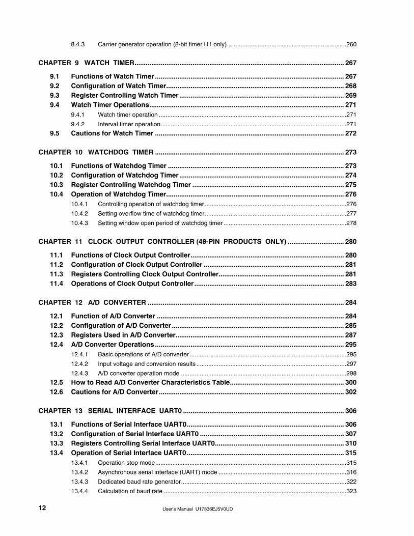
CHAPTER 9 WATCH TIMER................................................................................................................ 267
9.1 Functions of Watch Timer ..................................................................................................... 267 9.2 Configuration of Watch Timer............................................................................................... 268 9.3 Register Controlling Watch Timer........................................................................................ 269 9.4 Watch Timer Operations........................................................................................................ 271
9.4.1 Watch timer operation ..............................................................................................................271 9.4.2 Interval timer operation.............................................................................................................271
9.5 Cautions for Watch Timer ..................................................................................................... 272
CHAPTER 10 WATCHDOG TIMER ..................................................................................................... 273
10.1 Functions of Watchdog Timer .............................................................................................. 273 10.2 Configuration of Watchdog Timer........................................................................................ 274 10.3 Register Controlling Watchdog Timer ................................................................................. 275 10.4 Operation of Watchdog Timer............................................................................................... 276
10.4.1 Controlling operation of watchdog timer ...................................................................................276 10.4.2 Setting overflow time of watchdog timer...................................................................................277 10.4.3 Setting window open period of watchdog timer ........................................................................278
CHAPTER 11 CLOCK OUTPUT CONTROLLER (48-PIN PRODUCTS ONLY) .............................. 280
11.1 Functions of Clock Output Controller.................................................................................. 280 11.2 Configuration of Clock Output Controller ........................................................................... 281 11.3 Registers Controlling Clock Output Controller................................................................... 281 11.4 Operations of Clock Output Controller................................................................................ 283
CHAPTER 12 A/D CONVERTER ......................................................................................................... 284
12.1 Function of A/D Converter .................................................................................................... 284 12.2 Configuration of A/D Converter ............................................................................................ 285 12.3 Registers Used in A/D Converter.......................................................................................... 287 12.4 A/D Converter Operations ..................................................................................................... 295
12.4.1 Basic operations of A/D converter ............................................................................................295 12.4.2 Input voltage and conversion results ........................................................................................297 12.4.3 A/D converter operation mode .................................................................................................298
12.5 How to Read A/D Converter Characteristics Table............................................................. 300 12.6 Cautions for A/D Converter................................................................................................... 302
CHAPTER 13 SERIAL INTERFACE UART0 ...................................................................................... 306
13.1 Functions of Serial Interface UART0.................................................................................... 306 13.2 Configuration of Serial Interface UART0 ............................................................................. 307 13.3 Registers Controlling Serial Interface UART0..................................................................... 310 13.4 Operation of Serial Interface UART0.................................................................................... 315
13.4.1 Operation stop mode................................................................................................................315 13.4.2 Asynchronous serial interface (UART) mode ...........................................................................316 13.4.3 Dedicated baud rate generator.................................................................................................322 13.4.4 Calculation of baud rate ...........................................................................................................323
User’s Manual U17336EJ5V0UD 13
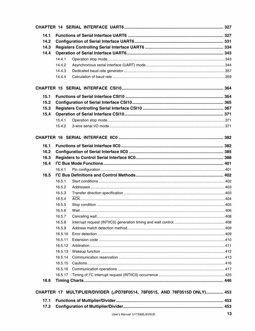
CHAPTER 14 SERIAL INTERFACE UART6...................................................................................... 327 14.1 Functions of Serial Interface UART6 ................................................................................... 327 14.2 Configuration of Serial Interface UART6............................................................................. 331 14.3 Registers Controlling Serial Interface UART6 .................................................................... 334 14.4 Operation of Serial Interface UART6.................................................................................... 343
14.4.1 Operation stop mode................................................................................................................343 14.4.2 Asynchronous serial interface (UART) mode ...........................................................................344 14.4.3 Dedicated baud rate generator ................................................................................................357 14.4.4 Calculation of baud rate ...........................................................................................................359
CHAPTER 15 SERIAL INTERFACE CSI10 ........................................................................................ 364
15.1 Functions of Serial Interface CSI10 ..................................................................................... 364 15.2 Configuration of Serial Interface CSI10 ............................................................................... 365 15.3 Registers Controlling Serial Interface CSI10 ...................................................................... 367 15.4 Operation of Serial Interface CSI10...................................................................................... 371
15.4.1 Operation stop mode................................................................................................................371 15.4.2 3-wire serial I/O mode..............................................................................................................371
CHAPTER 16 SERIAL INTERFACE IIC0 ........................................................................................... 382 16.1 Functions of Serial Interface IIC0......................................................................................... 382 16.2 Configuration of Serial Interface IIC0 .................................................................................. 385 16.3 Registers to Control Serial Interface IIC0............................................................................ 388 16.4 I2C Bus Mode Functions........................................................................................................ 401
16.4.1 Pin configuration ......................................................................................................................401 16.5 I2C Bus Definitions and Control Methods............................................................................ 402
16.5.1 Start conditions ........................................................................................................................402 16.5.2 Addresses ................................................................................................................................403 16.5.3 Transfer direction specification ................................................................................................403 16.5.4 ACK..........................................................................................................................................404 16.5.5 Stop condition ..........................................................................................................................405 16.5.6 Wait..........................................................................................................................................406 16.5.7 Canceling wait..........................................................................................................................408 16.5.8 Interrupt request (INTIIC0) generation timing and wait control.................................................408 16.5.9 Address match detection method.............................................................................................409 16.5.10 Error detection .........................................................................................................................409 16.5.11 Extension code ........................................................................................................................410 16.5.12 Arbitration.................................................................................................................................411 16.5.13 Wakeup function ......................................................................................................................412 16.5.14 Communication reservation .....................................................................................................413 16.5.15 Cautions...................................................................................................................................416 16.5.16 Communication operations ......................................................................................................417 16.5.17 Timing of I2C interrupt request (INTIIC0) occurrence ...............................................................425
16.6 Timing Charts......................................................................................................................... 446
CHAPTER 17 MULTIPLIER/DIVIDER (μPD78F0514, 78F0515, AND 78F0515D ONLY)............... 453
17.1 Functions of Multiplier/Divider ............................................................................................. 453 17.2 Configuration of Multiplier/Divider....................................................................................... 453

User’s Manual U17336EJ5V0UD 14
17.3 Register Controlling Multiplier/Divider ................................................................................ 457 17.4 Operations of Multiplier/Divider............................................................................................ 458
17.4.1 Multiplication operation.............................................................................................................458 17.4.2 Division operation.....................................................................................................................460
CHAPTER 18 INTERRUPT FUNCTIONS ............................................................................................ 462
18.1 Interrupt Function Types....................................................................................................... 462 18.2 Interrupt Sources and Configuration ................................................................................... 462 18.3 Registers Controlling Interrupt Functions .......................................................................... 466 18.4 Interrupt Servicing Operations ............................................................................................. 474
18.4.1 Maskable interrupt acknowledgment ........................................................................................474 18.4.2 Software interrupt request acknowledgment ............................................................................476 18.4.3 Multiple interrupt servicing........................................................................................................477 18.4.4 Interrupt request hold ...............................................................................................................480
CHAPTER 19 KEY INTERRUPT FUNCTION ..................................................................................... 481 19.1 Functions of Key Interrupt .................................................................................................... 481 19.2 Configuration of Key Interrupt.............................................................................................. 481 19.3 Register Controlling Key Interrupt ....................................................................................... 482
CHAPTER 20 STANDBY FUNCTION .................................................................................................. 483
20.1 Standby Function and Configuration................................................................................... 483 20.1.1 Standby function.......................................................................................................................483 20.1.2 Registers controlling standby function......................................................................................483
20.2 Standby Function Operation................................................................................................. 486 20.2.1 HALT mode ..............................................................................................................................486 20.2.2 STOP mode .............................................................................................................................491
CHAPTER 21 RESET FUNCTION........................................................................................................ 497
21.1 Register for Confirming Reset Source................................................................................. 505
CHAPTER 22 POWER-ON-CLEAR CIRCUIT...................................................................................... 506
22.1 Functions of Power-on-Clear Circuit ................................................................................... 506 22.2 Configuration of Power-on-Clear Circuit ............................................................................. 507 22.3 Operation of Power-on-Clear Circuit.................................................................................... 507 22.4 Cautions for Power-on-Clear Circuit .................................................................................... 510
CHAPTER 23 LOW-VOLTAGE DETECTOR ....................................................................................... 512
23.1 Functions of Low-Voltage Detector...................................................................................... 512 23.2 Configuration of Low-Voltage Detector ............................................................................... 513 23.3 Registers Controlling Low-Voltage Detector ...................................................................... 513 23.4 Operation of Low-Voltage Detector...................................................................................... 516
23.4.1 When used as reset .................................................................................................................517 23.4.2 When used as interrupt ............................................................................................................522
23.5 Cautions for Low-Voltage Detector...................................................................................... 527

User’s Manual U17336EJ5V0UD 15
CHAPTER 24 OPTION BYTE............................................................................................................... 530 24.1 Functions of Option Bytes.................................................................................................... 530 24.2 Format of Option Byte ........................................................................................................... 532
CHAPTER 25 FLASH MEMORY.......................................................................................................... 535
25.1 Internal Memory Size Switching Register ........................................................................... 535 25.2 Internal Expansion RAM Size Switching Register.............................................................. 536 25.3 Writing with Flash Memory Programmer............................................................................. 537 25.4 Programming Environment................................................................................................... 545 25.5 Communication Mode ........................................................................................................... 545 25.6 Handling of Pins on Board.................................................................................................... 547
25.6.1 FLMD0 pin ...............................................................................................................................547 25.6.2 Serial interface pins..................................................................................................................547 25.6.3 RESET pin ...............................................................................................................................549 25.6.4 Port pins...................................................................................................................................549 25.6.5 REGC pin.................................................................................................................................549 25.6.6 Other signal pins ......................................................................................................................549 25.6.7 Power supply ...........................................................................................................................550
25.7 Programming Method............................................................................................................ 551 25.7.1 Controlling flash memory .........................................................................................................551 25.7.2 Flash memory programming mode ..........................................................................................551 25.7.3 Selecting communication mode ...............................................................................................552 25.7.4 Communication commands......................................................................................................553
25.8 Security Settings.................................................................................................................... 554 25.9 Processing Time for Each Command When PG-FP4 Is Used (Reference) ...................... 556 25.10 Flash Memory Programming by Self Programming........................................................... 557
25.10.1 Boot swap function...................................................................................................................564
CHAPTER 26 ON-CHIP DEBUG FUNCTION (μPD78F0513D AND 78F0515D ONLY)................... 566
26.1 Connecting QB-78K0MINI or QB-MINI2 to μPD78F0513D and 78F0515D......................... 566 26.2 Reserved Area Used by QB-78K0MINI and QB-MINI2 ........................................................ 568
CHAPTER 27 INSTRUCTION SET ...................................................................................................... 569
27.1 Conventions Used in Operation List.................................................................................... 569 27.1.1 Operand identifiers and specification methods ........................................................................569 27.1.2 Description of operation column...............................................................................................570 27.1.3 Description of flag operation column........................................................................................570
27.2 Operation List......................................................................................................................... 571 27.3 Instructions Listed by Addressing Type ............................................................................. 579
CHAPTER 28 ELECTRICAL SPECIFICATIONS (STANDARD PRODUCTS)................................... 582
CHAPTER 29 ELECTRICAL SPECIFICATIONS ((A) GRADE PRODUCTS).................................... 603
CHAPTER 30 ELECTRICAL SPECIFICATIONS ((A2) GRADE PRODUCTS: TA = −40 to +110°C)........................................................................................................ 622

User’s Manual U17336EJ5V0UD 16
CHAPTER 31 ELECTRICAL SPECIFICATIONS ((A2) GRADE PRODUCTS: TA = −40 to +125°C)........................................................................................................ 641
CHAPTER 32 PACKAGE DRAWINGS ................................................................................................ 660
CHAPTER 33 RECOMMENDED SOLDERING CONDITIONS........................................................... 665
CHAPTER 34 CAUTIONS FOR WAIT................................................................................................. 666
34.1 Cautions for Wait.................................................................................................................... 666 34.2 Peripheral Hardware That Generates Wait .......................................................................... 667
APPENDIX A DEVELOPMENT TOOLS............................................................................................... 668
A.1 Software Package .................................................................................................................. 672 A.2 Language Processing Software............................................................................................ 672 A.3 Control Software .................................................................................................................... 673 A.4 Flash Memory Writing Tools ................................................................................................. 674
A.4.1 When using flash memory programmer PG-FP4, FL-PR4, PG-FPL3, and FP-LITE3 ..............674 A.4.2 When using on-chip debug emulator with programming function QB-MINI2 ............................674
A.5 Debugging Tools (Hardware) ................................................................................................ 675 A.5.1 When using in-circuit emulator QB-78K0KX2...........................................................................675 A.5.2 When using on-chip debug emulator QB-78K0MINI.................................................................676 A.5.3 When using on-chip debug emulator with programming function QB-MINI2 ............................676
A.6 Debugging Tools (Software) ................................................................................................. 677
APPENDIX B NOTES ON TARGET SYSTEM DESIGN ................................................................... 678
APPENDIX C REGISTER INDEX ......................................................................................................... 680
C.1 Register Index (In Alphabetical Order with Respect to Register Names) ........................ 680 C.2 Register Index (In Alphabetical Order with Respect to Register Symbol) ....................... 683
APPENDIX D LIST OF CAUTIONS..................................................................................................... 687
APPENDIX E REVISION HISTORY....................................................................................................... 713
E.1 Major Revisions in This Edition............................................................................................ 713 E.2 Revision History of Preceding Editions............................................................................... 719

User’s Manual U17336EJ5V0UD 17
CHAPTER 1 OUTLINE
1.1 Features
Minimum instruction execution time can be changed from high speed (0.1 μs: @ 20 MHz operation with high-
speed system clock) to ultra low-speed (122 μs: @ 32.768 kHz operation with subsystem clock)
General-purpose register: 8 bits × 32 registers (8 bits × 8 registers × 4 banks)
ROM, RAM capacities
Data Memory Item
Part Number
Program Memory (ROM) Internal High-Speed RAMNote Internal Expansion RAMNote
μPD78F0511 16 KB 768 bytes
μPD78F0512 24 KB
μPD78F0513, 78F0513D 32 KB
−
μPD78F0514 48 KB 1 KB
μPD78F0515, 78F0515D
Flash memoryNote
60 KB
1 KB
2 KB
Note The internal flash memory, internal high-speed RAM capacities, and internal expansion RAM capacities
can be changed using the internal memory size switching register (IMS) and the internal expansion RAM
size switching register (IXS). For IMS and IXS, see 25.1 Memory Size Switching Register and 25.2
Internal Expansion RAM Size Switching Register.
On-chip single-power-supply flash memory
Self-programming (with boot swap function)
On-chip debug function (μPD78F0513D and 78F0515D only)Note
On-chip power-on-clear (POC) circuit and low-voltage detector (LVI)
On-chip watchdog timer (operable with the on-chip internal low-speed oscillation clock)
On-chip multiplier/divider (16 bits × 16 bits, 32 bits / 16 bits)
(μPD78F0514, 78F0515, and 78F0515D only)
On-chip key interrupt function
On-chip clock output controller
I/O ports:
38-pin products: 31 (N-ch open drain: 4)
44-pin products: 37 (N-ch open drain: 4)
48-pin products: 41 (N-ch open drain: 4)
Note The μPD78F0513D and 78F0515D have on-chip debug functions. Do not use these products for mass
production because its reliability cannot be guaranteed after the on-chip debug function has been used, due
to issues with respect to the number of times the flash memory can be rewritten. NEC Electronics does not
accept complaints concerning these products.
<R>

CHAPTER 1 OUTLINE
User’s Manual U17336EJ5V0UD 18
Timer: 7 channels
• 16-bit timer/event counter: 1 channel
• 8-bit timer/event counter: 2 channels
• 8-bit timer: 2 channels
• Watch timer: 1 channel
• Watchdog timer: 1 channel
Serial interface: 3 channels
• UART (LIN (Local Interconnect Network)-bus supported: 1 channel
• CSI/UARTNote: 1 channel
• I2C: 1 channel
10-bit resolution A/D converter (AVREF = 2.3 to 5.5 V): 8 channels (38-pin products: 6 channels)
Power supply voltage
• Standard products, (A) grade products: VDD = 1.8 to 5.5 V
• (A2) grade products: VDD = 2.7 to 5.5 V
Operating ambient temperature
• Standard products, (A) grade products: TA = –40 to +85°C
• (A2) grade products: TA = –40 to +110°C, TA = –40 to +125°C
Note Select either of the functions of these alternate-function pins.
1.2 Applications
CHAPTER 1 OUTLINE
User’s Manual U17336EJ5V0UD 19
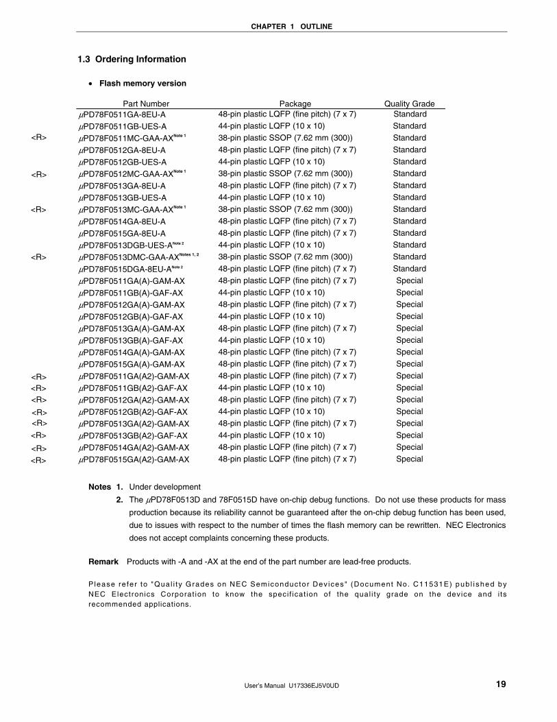
1.3 Ordering Information
• Flash memory version
Part Number Package Quality Grade μPD78F0511GA-8EU-A 48-pin plastic LQFP (fine pitch) (7 x 7) Standard
μPD78F0511GB-UES-A 44-pin plastic LQFP (10 x 10) Standard μPD78F0511MC-GAA-AXNote 1 38-pin plastic SSOP (7.62 mm (300)) Standard
μPD78F0512GA-8EU-A 48-pin plastic LQFP (fine pitch) (7 x 7) Standard μPD78F0512GB-UES-A 44-pin plastic LQFP (10 x 10) Standard μPD78F0512MC-GAA-AXNote 1 38-pin plastic SSOP (7.62 mm (300)) Standard
μPD78F0513GA-8EU-A 48-pin plastic LQFP (fine pitch) (7 x 7) Standard μPD78F0513GB-UES-A 44-pin plastic LQFP (10 x 10) Standard μPD78F0513MC-GAA-AXNote 1 38-pin plastic SSOP (7.62 mm (300)) Standard
μPD78F0514GA-8EU-A 48-pin plastic LQFP (fine pitch) (7 x 7) Standard μPD78F0515GA-8EU-A 48-pin plastic LQFP (fine pitch) (7 x 7) Standard μPD78F0513DGB-UES-ANote 2 44-pin plastic LQFP (10 x 10) Standard
μPD78F0513DMC-GAA-AXNotes 1, 2 38-pin plastic SSOP (7.62 mm (300)) Standard
μPD78F0515DGA-8EU-ANote 2 48-pin plastic LQFP (fine pitch) (7 x 7) Standard
μPD78F0511GA(A)-GAM-AX 48-pin plastic LQFP (fine pitch) (7 x 7) Special
μPD78F0511GB(A)-GAF-AX 44-pin plastic LQFP (10 x 10) Special
μPD78F0512GA(A)-GAM-AX 48-pin plastic LQFP (fine pitch) (7 x 7) Special
μPD78F0512GB(A)-GAF-AX 44-pin plastic LQFP (10 x 10) Special
μPD78F0513GA(A)-GAM-AX 48-pin plastic LQFP (fine pitch) (7 x 7) Special
μPD78F0513GB(A)-GAF-AX 44-pin plastic LQFP (10 x 10) Special
μPD78F0514GA(A)-GAM-AX 48-pin plastic LQFP (fine pitch) (7 x 7) Special
μPD78F0515GA(A)-GAM-AX 48-pin plastic LQFP (fine pitch) (7 x 7) Special
μPD78F0511GA(A2)-GAM-AX 48-pin plastic LQFP (fine pitch) (7 x 7) Special
μPD78F0511GB(A2)-GAF-AX 44-pin plastic LQFP (10 x 10) Special
μPD78F0512GA(A2)-GAM-AX 48-pin plastic LQFP (fine pitch) (7 x 7) Special
μPD78F0512GB(A2)-GAF-AX 44-pin plastic LQFP (10 x 10) Special
μPD78F0513GA(A2)-GAM-AX 48-pin plastic LQFP (fine pitch) (7 x 7) Special
μPD78F0513GB(A2)-GAF-AX 44-pin plastic LQFP (10 x 10) Special
μPD78F0514GA(A2)-GAM-AX 48-pin plastic LQFP (fine pitch) (7 x 7) Special
μPD78F0515GA(A2)-GAM-AX 48-pin plastic LQFP (fine pitch) (7 x 7) Special
Notes 1. Under development
2. The μPD78F0513D and 78F0515D have on-chip debug functions. Do not use these products for mass
production because its reliability cannot be guaranteed after the on-chip debug function has been used,
due to issues with respect to the number of times the flash memory can be rewritten. NEC Electronics
does not accept complaints concerning these products.
Remark Products with -A and -AX at the end of the part number are lead-free products.
P lease re fer to "Qual i ty Grades on NEC Semiconductor Dev ices" (Document No. C11531E) pub l i shed byNEC Electronics Corporat ion to know the speci f icat ion of the qual i ty grade on the device and i ts recommended applications.
<R>
<R>
<R>
<R>
<R> <R> <R>
<R> <R>
<R>
<R>
<R>

CHAPTER 1 OUTLINE
User’s Manual U17336EJ5V0UD 20
1.4 Pin Configuration (Top View)
• 38-pin plastic SSOP (7.62 mm (300))
1
2
3
4
5
6
7
8
9
10
11
12
13
14
15
16
17
18
19
ANI1/P21
ANI0/P20
P01/TI010/TO00
P00/TI000
P120/INTP0/EXLVI
RESET
P124/XT2/EXCLKS
P123/XT1
FLMD0
P122/X2/EXCLK/OCD0BNote
P121/X1/OCD0ANote
REGC
VSS
VDD
P60/SCL0
P61/SDA0
P62/EXSCL0
P63
P33/TI51/TO51/INTP4
ANI2/P22
ANI3/P23
ANI4/P24
ANI5/P25
AVSS
AVREF
P10/SCK10/TxD0
P11/SI10/RxD0
P12/SO10
P13/TxD6
P14/RxD6
P15/TOH0
P16/TOH1/INTP5
P17/TI50/TO50
P30/INTP1
P31/INTP2/OCD1ANote
P32/INTP3/OCD1BNote
P70/KR0
P71/KR1
38
37
36
35
34
33
32
31
30
29
28
27
26
25
24
23
22
21
20
Note μPD78F0513D (product with on-chip debug function) only
Cautions 1. Make AVSS the same potential as VSS.
2. Connect the REGC pin to VSS via a capacitor (0.47 to 1 μF: recommended).
3. ANI0/P20 to ANI5/P25 are set in the analog input mode after release of reset.
<R>
CHAPTER 1 OUTLINE
User’s Manual U17336EJ5V0UD 21
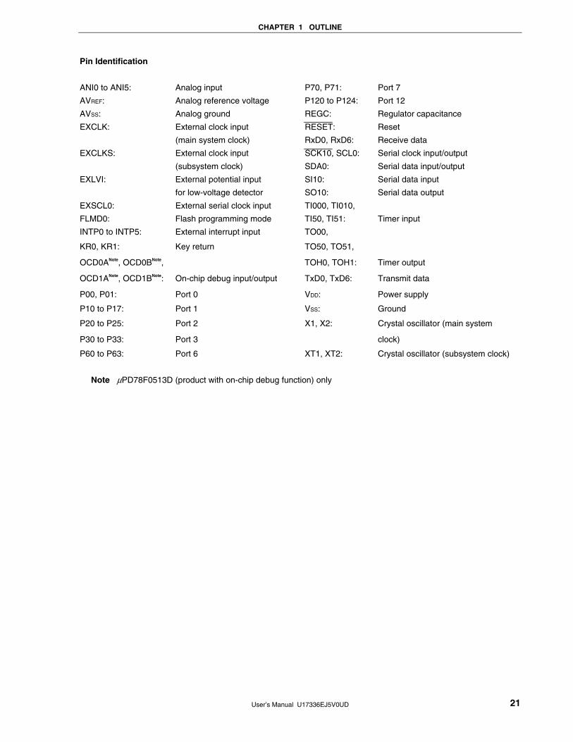
Pin Identification
ANI0 to ANI5: Analog input P70, P71: Port 7
AVREF: Analog reference voltage P120 to P124: Port 12
AVSS: Analog ground REGC: Regulator capacitance
EXCLK: External clock input RESET: Reset
(main system clock) RxD0, RxD6: Receive data
EXCLKS: External clock input SCK10, SCL0: Serial clock input/output
(subsystem clock) SDA0: Serial data input/output
EXLVI: External potential input SI10: Serial data input
for low-voltage detector SO10: Serial data output
EXSCL0: External serial clock input TI000, TI010,
FLMD0: Flash programming mode TI50, TI51: Timer input
INTP0 to INTP5: External interrupt input TO00,
KR0, KR1: Key return TO50, TO51,
OCD0ANote, OCD0BNote, TOH0, TOH1: Timer output
OCD1ANote, OCD1BNote: On-chip debug input/output TxD0, TxD6: Transmit data
P00, P01: Port 0 VDD: Power supply
P10 to P17: Port 1 VSS: Ground
P20 to P25: Port 2 X1, X2: Crystal oscillator (main system
P30 to P33: Port 3 clock)
P60 to P63: Port 6 XT1, XT2: Crystal oscillator (subsystem clock)
Note μPD78F0513D (product with on-chip debug function) only
CHAPTER 1 OUTLINE
User’s Manual U17336EJ5V0UD 22
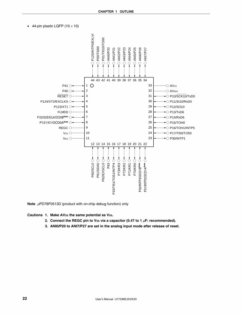
• 44-pin plastic LQFP (10 × 10)
1234567891011
3332313029282726252423
P41P40
RESETP124/XT2/EXCLKS
P123/XT1FLMD0
P122/X2/EXCLK/OCD0BNote
P121/X1/OCD0ANote
REGCVSS
VDD
AVSS
AVREF
P10/SCK10/TxD0P11/SI10/RxD0P12/SO10P13/TxD6P14/RxD6P15/TOH0P16/TOH1/INTP5P17/TI50/TO50P30/INTP1
12 13 14 15 16 17 18 19 20 21 22
44 43 42 41 40 39 38 37 36 35 34
P60
/SC
L0P
61/S
DA
0P
62/E
XS
CL0
P63
P33
/TI5
1/TO
51/IN
TP4
P73
/KR
3P
72/K
R2
P71
/KR
1P
70/K
R0
P32
/INTP
3/O
CD
1BN
ote
P31
/INTP
2/O
CD
1AN
ote
P12
0/IN
TP0/
EX
LVI
P00
/TI0
00P
01/T
I010
/TO
00A
NI0
/P20
AN
I1/P
21A
NI2
/P22
AN
I3/P
23A
NI4
/P24
AN
I5/P
25A
NI6
/P26
AN
I7/P
27
Note μPD78F0513D (product with on-chip debug function) only
Cautions 1. Make AVSS the same potential as VSS.
2. Connect the REGC pin to VSS via a capacitor (0.47 to 1 μF: recommended).
3. ANI0/P20 to ANI7/P27 are set in the analog input mode after release of reset.
CHAPTER 1 OUTLINE
User’s Manual U17336EJ5V0UD 23
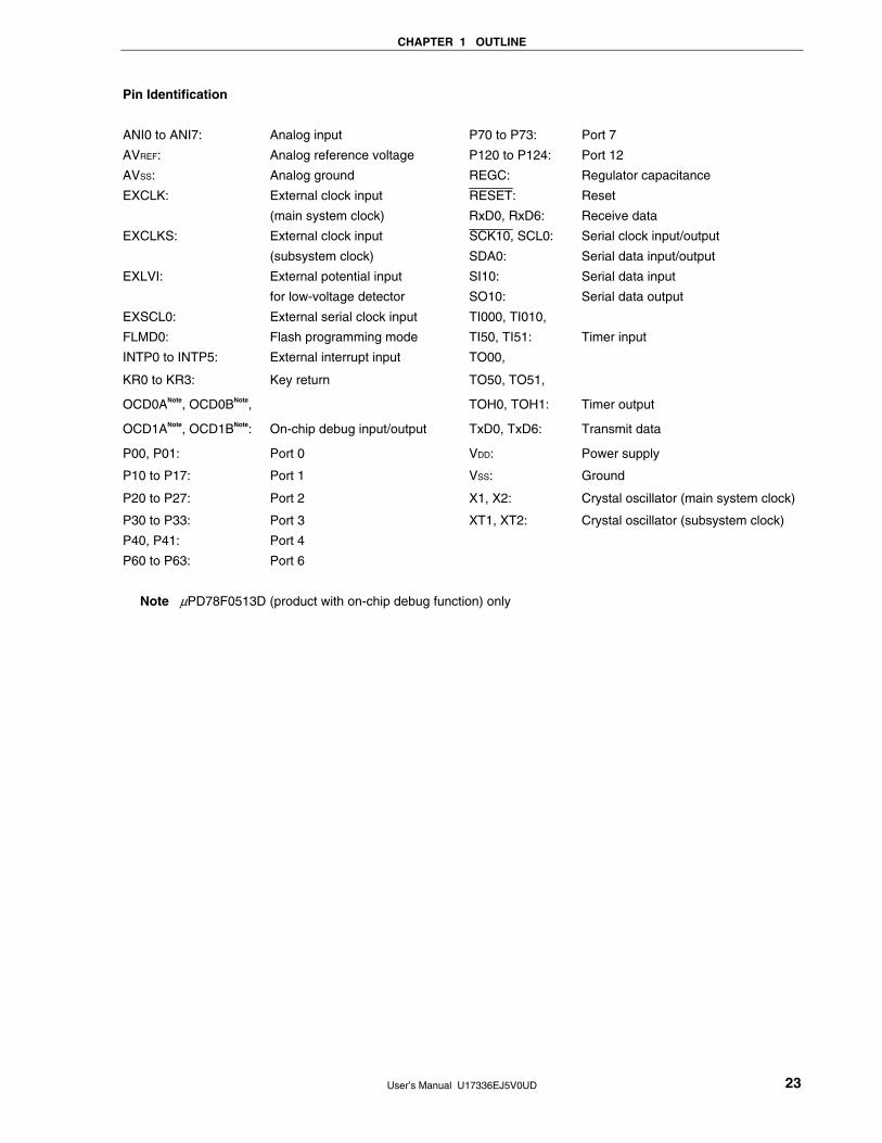
Pin Identification
ANI0 to ANI7: Analog input P70 to P73: Port 7
AVREF: Analog reference voltage P120 to P124: Port 12
AVSS: Analog ground REGC: Regulator capacitance
EXCLK: External clock input RESET: Reset
(main system clock) RxD0, RxD6: Receive data
EXCLKS: External clock input SCK10, SCL0: Serial clock input/output
(subsystem clock) SDA0: Serial data input/output
EXLVI: External potential input SI10: Serial data input
for low-voltage detector SO10: Serial data output
EXSCL0: External serial clock input TI000, TI010,
FLMD0: Flash programming mode TI50, TI51: Timer input
INTP0 to INTP5: External interrupt input TO00,
KR0 to KR3: Key return TO50, TO51,
OCD0ANote, OCD0BNote, TOH0, TOH1: Timer output
OCD1ANote, OCD1BNote: On-chip debug input/output TxD0, TxD6: Transmit data
P00, P01: Port 0 VDD: Power supply
P10 to P17: Port 1 VSS: Ground
P20 to P27: Port 2 X1, X2: Crystal oscillator (main system clock)
P30 to P33: Port 3 XT1, XT2: Crystal oscillator (subsystem clock)
P40, P41: Port 4
P60 to P63: Port 6
Note μPD78F0513D (product with on-chip debug function) only

CHAPTER 1 OUTLINE
User’s Manual U17336EJ5V0UD 24
• 48-pin plastic LQFP (fine pitch) (7 × 7)
P60/SCL0P61/SDA0
P62/EXSCL0P63
P33/TI51/TO51/INTP4P75P74
P73/KR3P72/KR2P71/KR1P70/KR0
P32/INTP3/OCD1BNote
123456789
101112
48 47 46 45 44 43 42 41 40 39 38 37
13 14 15 16 17 18 19 20 21 22 23 24
363534333231302928272625
P140/PCL/INTP6P00/TI000P01/TI010/TO00P130P20/ANI0ANI1/P21ANI2/P22ANI3/P23ANI4/P24ANI5/P25ANI6/P26ANI7/P27
P31
/INTP
2/O
CD
1AN
ote
P30
/INT
P1
P17
/TI5
0/T
O50
P16
/TO
H1/
INT
P5
P15
/TO
H0
P14
/RxD
6P
13/T
xD6
P12
/SO
10P
11/S
l10/
RxD
0P
10/S
CK
10/T
xD0
AV
RE
F
AV
SS
VD
D
VS
S
RE
GC
P12
1/X
1/O
CD
0AN
ote
P122
/X2/
EXCL
K/O
CD0B
Not
e
FLM
D0
P12
3/X
T1
P12
4/X
T2/
EX
CLK
SR
ES
ET
P40
P41
P12
0/IN
TP
0/E
XLV
I
Note μPD78F0515D (product with on-chip debug function) only
Cautions 1. Make AVSS the same potential as VSS.
2. Connect the REGC pin to VSS via a capacitor (0.47 to 1 μF: recommended).
3. ANI0/P20 to ANI7/P27 are set in the analog input mode after release of reset.
CHAPTER 1 OUTLINE
User’s Manual U17336EJ5V0UD 25
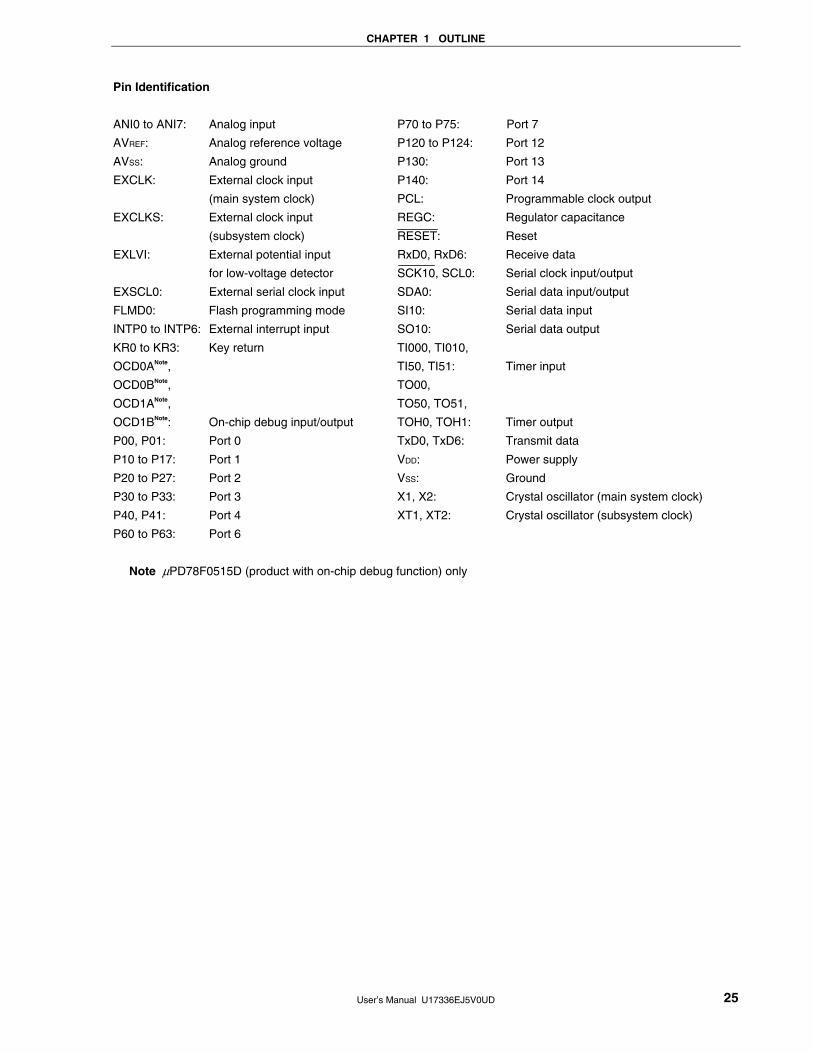
Pin Identification
ANI0 to ANI7: Analog input
AVREF: Analog reference voltage
AVSS: Analog ground
EXCLK: External clock input
(main system clock)
EXCLKS: External clock input
(subsystem clock)
EXLVI: External potential input
for low-voltage detector
EXSCL0: External serial clock input
FLMD0: Flash programming mode
INTP0 to INTP6: External interrupt input
KR0 to KR3: Key return
OCD0ANote,
OCD0BNote,
OCD1ANote,
OCD1BNote: On-chip debug input/output
P00, P01: Port 0
P10 to P17: Port 1
P20 to P27: Port 2
P30 to P33: Port 3
P40, P41: Port 4
P60 to P63: Port 6
P70 to P75: Port 7
P120 to P124: Port 12
P130: Port 13
P140: Port 14
PCL: Programmable clock output
REGC: Regulator capacitance
RESET: Reset
RxD0, RxD6: Receive data
SCK10, SCL0: Serial clock input/output
SDA0: Serial data input/output
SI10: Serial data input
SO10: Serial data output
TI000, TI010,
TI50, TI51: Timer input
TO00,
TO50, TO51,
TOH0, TOH1: Timer output
TxD0, TxD6: Transmit data
VDD: Power supply
VSS: Ground
X1, X2: Crystal oscillator (main system clock)
XT1, XT2: Crystal oscillator (subsystem clock)
Note μPD78F0515D (product with on-chip debug function) only
CHAPTER 1 OUTLINE
User’s Manual U17336EJ5V0UD 26
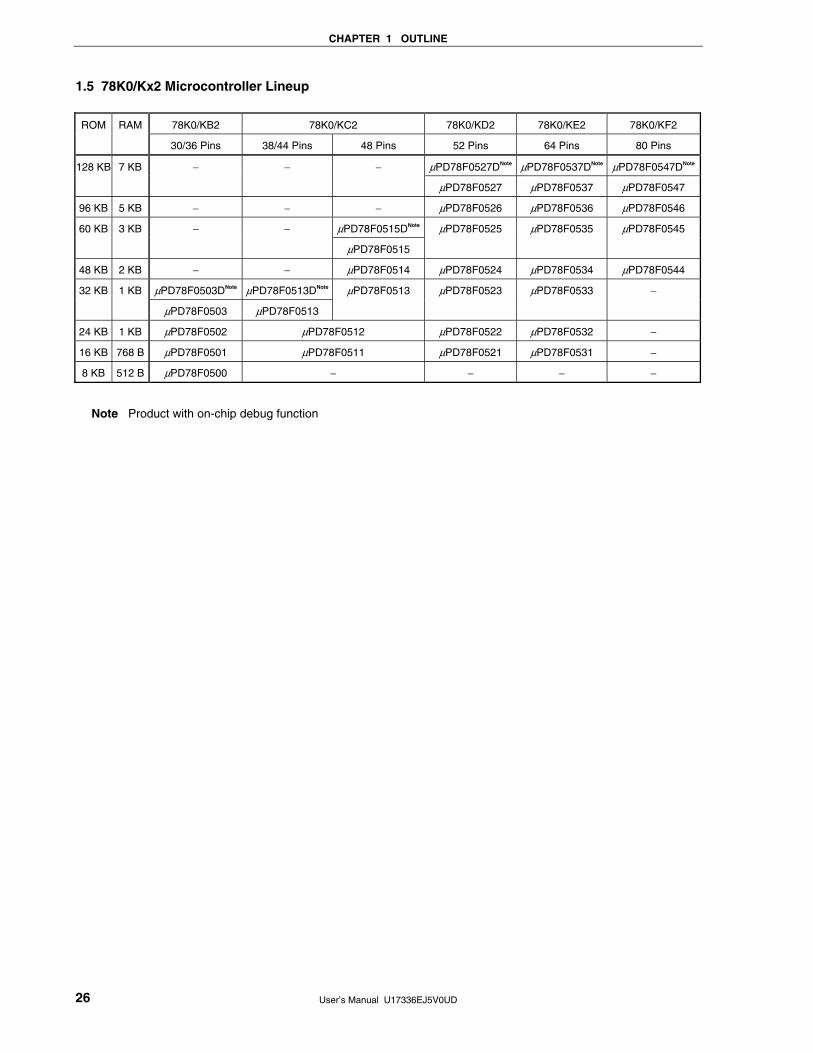
1.5 78K0/Kx2 Microcontroller Lineup
78K0/KB2 78K0/KC2 78K0/KD2 78K0/KE2 78K0/KF2 ROM RAM
30/36 Pins 38/44 Pins 48 Pins 52 Pins 64 Pins 80 Pins
μPD78F0527DNote μPD78F0537DNote μPD78F0547DNote128 KB 7 KB − − −
μPD78F0527 μPD78F0537 μPD78F0547
96 KB 5 KB − − − μPD78F0526 μPD78F0536 μPD78F0546
μPD78F0515DNote60 KB 3 KB − −
μPD78F0515
μPD78F0525 μPD78F0535 μPD78F0545
48 KB 2 KB − − μPD78F0514 μPD78F0524 μPD78F0534 μPD78F0544
μPD78F0503DNote μPD78F0513DNote32 KB 1 KB
μPD78F0503 μPD78F0513
μPD78F0513 μPD78F0523 μPD78F0533 −
24 KB 1 KB μPD78F0502 μPD78F0512 μPD78F0522 μPD78F0532 −
16 KB 768 B μPD78F0501 μPD78F0511 μPD78F0521 μPD78F0531 −
8 KB 512 B μPD78F0500 − − − −
Note Product with on-chip debug function

CHAPTER 1 OUTLINE
User’s Manual U17336EJ5V0UD 27
The list of functions of the 78K0/Kx2 microcontrollers is shown below. (1/2)
78K0/KB2 78K0/KC2 Part Number
Item 30/36 Pins 38/44 Pins 48 Pins
Flash memory (KB) 8 16 24 32 16 24 32 16 24 32 48 60
RAM (KB) 0.5 0.75 1 1 0.75 1 1 0.75 1 1 2 3
Bank (flash memory) −
Power supply voltage • Standard products, (A) grade products: VDD = 1.8 to 5.5 V • (A2) grade products: VDD = 2.7 to 5.5 V
Regulator Provided
Minimum instruction execution time
0.1 μs (20 MHz: VDD = 4.0 to 5.5 V)/0.2 μs (10 MHz: VDD = 2.7 to 5.5 V)/ 0.4 μs (5 MHz: VDD = 1.8 to 5.5 V)
High-speed system 20 MHz: VDD = 4.0 to 5.5 V/10 MHz: VDD = 2.7 to 5.5 V/5 MHz: VDD = 1.8 to 5.5 V
Mai
n
Internal high-speed oscillation
8 MHz (TYP.): VDD = 1.8 to 5.5 V
Subsystem − 32.768 kHz (TYP.): VDD = 1.8 to 5.5 V Clo
ck
Internal low-speed oscillation
240 kHz (TYP.): VDD = 1.8 to 5.5 V
Total 23 31 (38 Pins)/ 37 (44 Pins)
41
Por
t
N-ch O.D. (6 V tolerance)
2 4 4
16 bits (TM0) 1 ch
8 bits (TM5) 2 ch
8 bits (TMH) 2 ch
Watch − 1 ch
Tim
er
WDT 1 ch
3-wire CSI −
Automatic transmit/ receive 3-wire CSI
−
UART/3-wire CSINote 1 ch
UART supporting LIN-bus
1 ch
Ser
ial i
nter
face
I2C bus 1 ch
10-bit A/D 4 ch 6 ch (38 Pins)/ 8 ch (44 Pins)
8 ch
External 6 7 8
Inte
rrup
t
Internal 14 16
Key interrupt − 2 ch (38 Pins)/ 4 ch (44 Pins)
4 ch
RESET pin Provided
POC 1.59 V ±0.15 V (rise time to 1.8 V: 3.6 ms (MAX.))
LVI The detection level of the supply voltage is selectable in 16 steps. Res
et
WDT Provided
Clock output/buzzer output − Clock output only
Multiplier/divider − Provided
On-chip debug function μPD78F0503D only μPD78F0513D only μPD78F0515D only
Operating ambient temperature
• Standard products, (A) grade products: TA = –40 to +85°C • (A2) grade products: TA = –40 to +110°C, TA = –40 to +125°C
Note Select either of the functions of these alternate-function pins.
<R>
<R>
<R>
<R>
<R>

CHAPTER 1 OUTLINE
User’s Manual U17336EJ5V0UD 28
(2/2)
78K0/KD2 78K0/KE2 78K0/KF2 Part Number
Item 52 Pins 64 Pins 80 Pins
Flash memory (KB) 16 24 32 48 60 96 128 16 24 32 48 60 96 128 48 60 96 128
RAM (KB) 0.75 1 1 2 3 5 7 0.75 1 1 2 3 5 7 2 3 5 7
Bank (flash memory) − 4 6 − 4 6 − 4 6
Power supply voltage • Standard products, (A) grade products: VDD = 1.8 to 5.5 V • (A2) grade products: VDD = 2.7 to 5.5 V
Regulator Provided
Minimum instruction execution time
0.1 μs (20 MHz: VDD = 4.0 to 5.5 V)/0.2 μs (10 MHz: VDD = 2.7 to 5.5 V)/ 0.4 μs (5 MHz: VDD = 1.8 to 5.5 V)
High-speed system 20 MHz: VDD = 4.0 to 5.5 V/10 MHz: VDD = 2.7 to 5.5 V/5 MHz: VDD = 1.8 to 5.5 V
Mai
n
Internal high-speed oscillation
8 MHz (TYP.): VDD = 1.8 to 5.5 V
Subsystem 32.768 kHz (TYP.): VDD = 1.8 to 5.5 V Clo
ck
Internal low-speed oscillation
240 kHz (TYP.): VDD = 1.8 to 5.5 V
Total 45 55 71
Por
t
N-ch O.D. (6 V tolerance)
4 4 4
16 bits (TM0) 1 ch 2 ch
8 bits (TM5) 2 ch
8 bits (TMH) 2 ch
Watch 1 ch
Tim
er
WDT 1 ch
3-wire CSI − 1 ch
Automatic transmit/ receive 3-wire CSI
− 1 ch
UART/3-wire CSINote 1 ch
UART supporting LIN-bus
1 ch
Ser
ial i
nter
face
I2C bus 1 ch
10-bit A/D 8 ch
External 8 9
Inte
rrup
t
Internal 16 19 20
Key interrupt 8 ch
RESET pin Provided
POC 1.59 V ±0.15 V (rise time to 1.8 V: 3.6 ms (MAX.))
LVI The detection level of the supply voltage is selectable in 16 steps. Res
et
WDT Provided
Clock output/buzzer output Clock output only Provided
Multiplier/divider − Provided − Provided
On-chip debug function μPD78F0527D only μPD78F0537D only μPD78F0547D only
Operating ambient temperature
• Standard products, (A) grade products: TA = –40 to +85°C • (A2) grade products: TA = –40 to +110°C, TA = –40 to +125°C
Note Select either of the functions of these alternate-function pins.
<R>
<R>
CHAPTER 1 OUTLINE
User’s Manual U17336EJ5V0UD 29
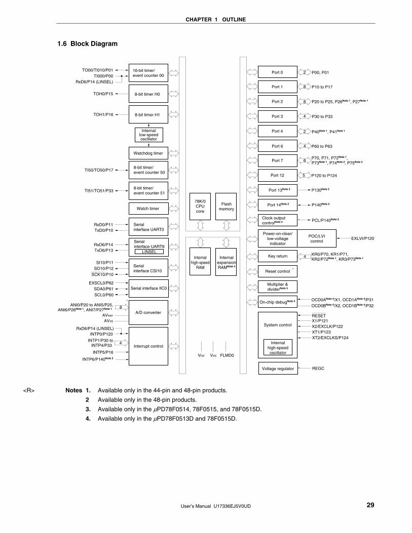
1.6 Block Diagram
Port 0 P00, P012
Port 1 P10 to P17
Port 2 P20 to P25, P26Note 1, P27Note 18
Port 3 P30 to P334
Port 4
VSS FLMD0 VDD
8
Power-on-clear/low-voltage
indicator
POC/LVIcontrol
Reset control
Port 6 P60 to P634
Port 7P70, P71, P72Note 1, P73Note 1, P74Note 2, P75Note 2
Port 12 P120 to P124
Port 13Note 2 P130Note 2
6
P40Note 1, P41Note 12
Port 14Note 2 P140Note 2
Clock outputcontrolNote 2 PCL/P140Note 2
Key return 4 KR0/P70, KR1/P71, KR2/P72Note 1, KR3/P73Note 1
EXLVI/P120
System control
RESETX1/P121X2/EXCLK/P122XT1/P123XT2/EXCLKS/P124
ANI0/P20 to ANI5/P25,ANI6/P26Note 1, ANI7/P27Note 1
Interrupt control
8A/D converter
AVREF
AVSS
INTP1/P30 toINTP4/P33
4
INTP0/P120
Serial interface IIC0EXSCL0/P62
SDA0/P61SCL0/P60
INTP5/P16
INTP6/P140Note 2
Internalhigh-speed
RAM
InternalexpansionRAMNote 3
78K/0CPUcore
Flashmemory
8-bit timer H0TOH0/P15
8-bit timer H1TOH1/P16
TI50/TO50/P178-bit timer/event counter 50
RxD0/P11TxD0/P10
Serial interface UART0
Watchdog timer
RxD6/P14TxD6/P13
Serial interface UART6
TI51/TO51/P338-bit timer/event counter 51
Watch timer
Serial interface CSI10
SI10/P11SO10/P12
SCK10/P10
16-bit timer/event counter 00
TO00/TI010/P01TI000/P00
Multiplier ÷rNote 3
On-chip debugNote 4
RxD6/P14 (LINSEL)
RxD6/P14 (LINSEL)
LINSEL
5
OCD0ANote 4/X1, OCD1ANote 4/P31OCD0BNote 4/X2, OCD1BNote 4/P32
Internallow-speedoscillator
Internalhigh-speedoscillator
Voltage regulator REGC
Notes 1. Available only in the 44-pin and 48-pin products.
2 Available only in the 48-pin products.
3. Available only in the μPD78F0514, 78F0515, and 78F0515D.
4. Available only in the μPD78F0513D and 78F0515D.
<R>

CHAPTER 1 OUTLINE
User’s Manual U17336EJ5V0UD 30
1.7 Outline of Functions (1/2)
Item μPD78F0511 μPD78F0512 μPD78F0513 μPD78F0513D μPD78F0514 μPD78F0515 μPD78F0515D
Flash memory (self-programming supported)Note
16 K 24 K 32 K 48 K 60 K
High-speed RAMNote 768 1 K
Internal memory (bytes)
Expansion RAMNote − 1 K 2 K
Memory space 64 KB
High-speed X1 (crystal/ceramic) oscillation, external main system clock input (EXCLK)
Standard products, (A) grade products
1 to 20 MHz: VDD = 4.0 to 5.5 V, 1 to 10 MHz: VDD = 2.7 to 5.5 V,
1 to 5 MHz: VDD = 1.8 to 5.5 V
system
clock
(A2) grade products
1 to 20 MHz: VDD = 4.0 to 5.5 V, 1 to 10 MHz: VDD = 2.7 to 5.5 V
Internal high-speed oscillation
Internal oscillation
Standard products, (A) grade products
8 MHz (TYP.): VDD = 1.8 to 5.5 V
Main system clock (oscillation frequency)
clock
(A2) grade products
8 MHz (TYP.): VDD = 2.7 to 5.5 V
Subsystem clock XT1 (crystal) oscillation, external subsystem clock input (EXCLKS)
Standard products, (A) grade products
32.768 kHz (TYP.): VDD = 1.8 to 5.5 V (oscillation
frequency)
(A2) grade products
32.768 kHz (TYP.): VDD = 2.7 to 5.5 V
Internal low-speed Internal oscillation
Standard products, (A) grade products
240 kHz (TYP.): VDD = 1.8 to 5.5 V oscillation clock
(for TMH1, WDT)
(A2) grade products
240 kHz (TYP.): VDD = 2.7 to 5.5 V
General-purpose registers 8 bits × 32 registers (8 bits × 8 registers × 4 banks)
0.1 μs (high-speed system clock: @ fXH = 20 MHz operation)
0.25 μs (internal high-speed oscillation clock: @ fRH = 8 MHz (TYP.) operation)
Minimum instruction execution time
122 μs (subsystem clock: @ fSUB = 32.768 kHz operation)
Note The internal flash memory capacity, internal high-speed RAM capacity, and internal expansion RAM capacity
can be changed using the internal memory size switching register (IMS) and the internal expansion RAM size
switching register (IXS).

CHAPTER 1 OUTLINE
User’s Manual U17336EJ5V0UD 31
(2/2)
Item μPD78F0511 μPD78F0512 μPD78F0513 μPD78F0513D μPD78F0514 μPD78F0515 μPD78F0515D
Instruction set • 8-/16-bit operation • Multiply/divide (8 bits × 8 bits, 16 bits ÷ 8 bits) • Bit manipulate (set, reset, test, and Boolean operation) • BCD adjust, etc.
I/O ports Total: 31 (38-pin products) 37 (44-pin products) 41 (48-pin products)
CMOS I/O: 27 33 36
CMOS output: 0 0 1
N-ch open-drain I/O
(6 V tolerance): 4 4 4
Timers • 16-bit timer/event counter: 1 channel • 8-bit timer/event counter: 2 channels • 8-bit timer: 2 channels • Watch timer: 1 channel • Watchdog timer: 1 channel
Timer outputs 5 (PWM output: 4, PPG output: 1)
Clock output
(48-pin products only)
• 156.25 kHz, 312.5 kHz, 625 kHz, 1.25 MHz, 2.5 MHz, 5 MHz, 10 MHz (peripheral hardware clock: @ fPRS = 20 MHz operation) • 32.768 kHz (subsystem clock: @ fSUB = 32.768 kHz operation)
A/D converter • 38-pin products: 10-bit resolution × 6 channels (AVREF = 2.3 to 5.5 V) • 44-pin, 48-pin products: 10-bit resolution × 8 channels (AVREF = 2.3 to 5.5 V)
Serial interface • UART mode supporting LIN-bus: 1 channel • 3-wire serial I/O mode/UART modeNote: 1 channel • I2C bus mode: 1 channel
Multiplier/divider − • 16 bits × 16 bits = 32 bits (multiplication) • 32 bits ÷ 16 bits = 32 bits remainder of 16 bits (division)
Internal 16 Vectored interrupt sources External 7 (38-pin, 44-pin products), 8 (48-pin products)
Key interrupt Key interrupt (INTKR) occurs by detecting falling edge of key input pins (KR0 and KR1 (38-pin products), KR0 to KR3 (44-pin, 48-pin products)).
Reset • Reset using RESET pin • Internal reset by watchdog timer • Internal reset by power-on-clear • Internal reset by low-voltage detector
On-chip debug function − Provided − Provided
Power supply voltage • Standard products, (A) grade products: VDD = 1.8 to 5.5 V • (A2) grade products: VDD = 2.7 to 5.5 V
Operating ambient temperature
• Standard products, (A) grade products: TA = –40 to +85°C • (A2) grade products: TA = –40 to +110°C, TA = –40 to +125°C
Package • 38-pin plastic SSOP (7.62 mm (300)) • 44-pin plastic LQFP (10 × 10) • 48-pin plastic LQFP (fine pitch) (7 × 7)
Note Select either of the functions of these alternate-function pins.
<R>
<R>
<R>

CHAPTER 1 OUTLINE
User’s Manual U17336EJ5V0UD 32
An outline of the timer is shown below.
16-bit Timer/ Event Counter
00
8-bit Timer/ Event Counters
50 and 51
8-bit Timers H0 and H1
TM00 TM50 TM51 TMH0 TMH1
Watch Timer
Watchdog Timer
Interval timer 1 channel 1 channel 1 channel 1 channel 1 channel 1 channelNote 1 −
External event counter
1 channel 1 channel 1 channel − − − −
PPG output 1 output − − − − − −
PWM output − 1 output 1 output 1 output 1 output − −
Pulse width measurement
2 inputs − − − − − −
Square-wave output
1 output 1 output 1 output 1 output 1 output − −
Carrier generator − − − − 1 output Note 2 − −
Watch timer − − − − − 1 channelNote 1 −
Function
Watchdog timer − − − − − − 1 channel
Interrupt source 2 1 1 1 1 1 −
Notes 1. In the watch timer, the watch timer function and interval timer function can be used simultaneously.
2. TM51 and TMH1 can be used in combination as a carrier generator mode.

User’s Manual U17336EJ5V0UD 33
CHAPTER 2 PIN FUNCTIONS
2.1 Pin Function List
There are two types of pin I/O buffer power supplies: AVREF and VDD. The relationship between these power
supplies and the pins is shown below.
Table 2-1. Pin I/O Buffer Power Supplies
Power Supply Corresponding Pins
AVREF P20 to P27
VDD Pins other than P20 to P27
(1) Port functions (1/2)
Function Name I/O Function After Reset Alternate Function
P00 TI000
P01
I/O Port 0.
2-bit I/O port.
Input/output can be specified in 1-bit units.
Use of an on-chip pull-up resistor can be specified by a software
setting.
Input port
TI010/TO00
P10 SCK10/TxD0
P11 SI10/RxD0
P12 SO10
P13 TxD6
P14 RxD6
P15 TOH0
P16 TOH1/INTP5
P17
I/O Port 1.
8-bit I/O port.
Input/output can be specified in 1-bit units.
Use of an on-chip pull-up resistor can be specified by a software
setting.
Input port
TI50/TO50
P20 to P25 ANI0 to ANI7
P26Note 1, P27Note 1
I/O Port 2.
8-bit I/O port.
Input/output can be specified in 1-bit units.
Analog input
ANI6Note 1, ANI7Note 1
P30 INTP1
P31 INTP2/OCD1ANote 2
P32 INTP3/OCD1BNote 2
P33
I/O Port 3. 4-bit I/O port. Input/output can be specified in 1-bit units. Use of an on-chip pull-up resistor can be specified by a software
setting.
Input port
TI51/TO51/INTP4
Notes 1. 44-pin and 48-pin products only
For the 38-pin products, be sure to set bits 6 and 7 of PM2 to “1”, and bits 6 and 7 of P2 to “0”.
2. μPD78F0513D and 78F0515D only
<R>
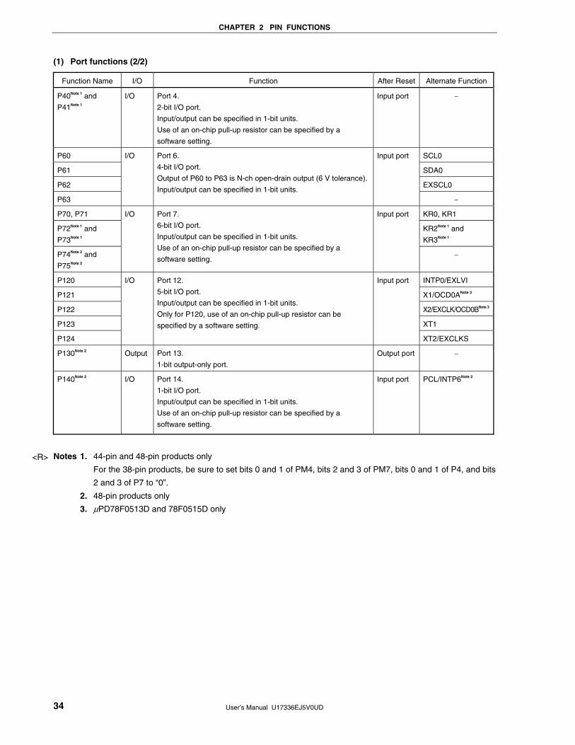
CHAPTER 2 PIN FUNCTIONS
User’s Manual U17336EJ5V0UD 34
(1) Port functions (2/2)
Function Name I/O Function After Reset Alternate Function
P40Note 1 and
P41Note 1
I/O Port 4.
2-bit I/O port.
Input/output can be specified in 1-bit units.
Use of an on-chip pull-up resistor can be specified by a
software setting.
Input port −
P60 SCL0
P61 SDA0
P62 EXSCL0
P63
I/O Port 6.
4-bit I/O port.
Output of P60 to P63 is N-ch open-drain output (6 V tolerance).
Input/output can be specified in 1-bit units.
Input port
−
P70, P71 KR0, KR1
P72Note 1 and
P73Note 1
KR2Note 1 and
KR3Note 1
P74Note 2 and
P75Note 2
I/O Port 7.
6-bit I/O port.
Input/output can be specified in 1-bit units.
Use of an on-chip pull-up resistor can be specified by a
software setting.
Input port
−
P120 INTP0/EXLVI
P121 X1/OCD0ANote 3
P122 X2/EXCLK/OCD0BNote 3
P123 XT1
P124
I/O Port 12.
5-bit I/O port.
Input/output can be specified in 1-bit units.
Only for P120, use of an on-chip pull-up resistor can be
specified by a software setting.
Input port
XT2/EXCLKS
P130Note 2 Output Port 13.
1-bit output-only port.
Output port −
P140Note 2 I/O Port 14.
1-bit I/O port.
Input/output can be specified in 1-bit units.
Use of an on-chip pull-up resistor can be specified by a
software setting.
Input port PCL/INTP6Note 2
Notes 1. 44-pin and 48-pin products only
For the 38-pin products, be sure to set bits 0 and 1 of PM4, bits 2 and 3 of PM7, bits 0 and 1 of P4, and bits
2 and 3 of P7 to “0”.
2. 48-pin products only
3. μPD78F0513D and 78F0515D only
<R>

CHAPTER 2 PIN FUNCTIONS
User’s Manual U17336EJ5V0UD 35
(2) Non-port functions (1/2)
Function Name I/O Function After Reset Alternate Function
ANI0 to ANI5 P20 to P25
ANI6Note 1, ANI7Note 1
Input A/D converter analog input Analog input
P26Note 1, P27Note 1
EXLVI Input Potential input for external low-voltage detection Input port P120/INTP0
EXSCL0 Input External clock input for serial interface.
To input an external clock, input a clock of 6.4 MHz.
Input port P62
FLMD0 − Flash memory programming mode setting − −
INTP0 P120/EXLVI
INTP1 P30
INTP2 P31/OCD1ANote 2
INTP3 P32/OCD1BNote 2
INTP4 P33/TI51/TO51
INTP5 P16/TOH1
INTP6Note 3
Input External interrupt request input for which the valid edge (rising
edge, falling edge, or both rising and falling edges) can be
specified
Input port
P140/PCLNote 3
KR0, KR1 P70, P71
KR2Note 1 and
KR3Note 1
Input Key interrupt input Input port
P72Note 1 and
P73Note 1
PCLNote 3 Output Clock output (for trimming of high-speed system clock,
subsystem clock)
Input port P140/INTP6Note 3
REGC − Connecting regulator output (2.5 V) stabilization capacitance
for internal operation.
Connect to VSS via a capacitor (0.47 to 1 μF: recommended).
− −
RESET Input System reset input − −
RxD0 P11/SI10
RxD6
Input Serial data input to asynchronous serial interface Input port
P14
SCK10 P10/TxD0
SCL0
I/O Clock input/output for serial interface Input port
P60
SDA0 I/O Serial data I/O for serial interface Input port P61
SI10 Input Serial data input to serial interface Input port P11/RxD0
SO10 Output Serial data output from serial interface Input port P12
TI000 External count clock input to 16-bit timer/event counter 00
Capture trigger input to capture registers (CR000, CR010) of
16-bit timer/event counter 00
P00
TI010
Input
Capture trigger input to capture register (CR000) of 16-bit
timer/event counter 00
Input port
P01/TO00
TI50 External count clock input to 8-bit timer/event counter 50 P17/TO50
TI51
Input
External count clock input to 8-bit timer/event counter 51
Input port
P33/TO51/INTP4
TO00 Output 16-bit timer/event counter 00 output Input port P01/TI010
Notes 1. 44-pin and 48-pin products only
For the 38-pin products, be sure to set bits 6 and 7 of PM2 to “1”, and bits 2 and 3 of PM7, bits 6 and 7 of
P2, and bits 2 and 3 of P7 to “0”.
2. μPD78F0513D and 78F0515D only
3. 48-pin products only
<R>

CHAPTER 2 PIN FUNCTIONS
User’s Manual U17336EJ5V0UD 36
(2) Non-port pins (2/2)
Function Name I/O Function After Reset Alternate Function
TO50 8-bit timer/event counter 50 output P17/TI50
TO51
Output
8-bit timer/event counter 51 output
Input port
P33/TI51/INTP4
TOH0 8-bit timer H0 output P15
TOH1
Output
8-bit timer H1 output
Input port
P16/INTP5
TxD0 P10/SCK10
TxD6
Output Serial data output from asynchronous serial interface Input port
P13
X1 Input P121/OCD0ANote
X2 −
Connecting resonator for main system clock Input port
P122/EXCLK/
OCD0BNote
EXCLK Input External clock input for main system clock Input port P122/X2/
OCD0BNote
XT1 Input Input port P123
XT2 −
Connecting resonator for subsystem clock
Input port P124/EXCLKS
EXCLKS Input External clock input for subsystem clock Input port P124/XT2
VDD − Positive power supply for pins other than P20 to P27 − −
AVREF Input A/D converter reference voltage input and positive power
supply for P20 to P27 and A/D converter
− −
VSS − Ground potential for pins other than P20 to P27 − −
AVSS − A/D converter ground potential. Make the same potential as
VSS.
− −
OCD0ANote P121/X1
OCD1ANote
Input
P31/INTP2
OCD0BNote P122/X2/EXCLK
OCD1BNote
−
Connection for on-chip debug mode setting pins
(μPD78F0513D and 78F0515D only)
Input port
P32/INTP3
Note μPD78F0513D and 78F0515D only
2.2 Description of Pin Functions
2.2.1 P00 and P01 (port 0)
P00 and P01 function as a 2-bit I/O port. These pins also function as timer I/O.
The following operation modes can be specified in 1-bit units.
(1) Port mode
P00 and P01 function as a 2-bit I/O port. P00 and P01 can be set to input or output port in 1-bit units using port
mode register 0 (PM0). Use of an on-chip pull-up resistor can be specified by pull-up resistor option register 0
(PU0).
(2) Control mode
P00 and P01 function as timer I/O.
(a) TI000
This is a pin for inputting an external count clock to 16-bit timer/event counter and is also for inputting a
capture trigger signal to the capture registers (CR000, CR010) of 16-bit timer/event counter 00.

CHAPTER 2 PIN FUNCTIONS
User’s Manual U17336EJ5V0UD 37
(b) TI010
This is a pin for inputting a capture trigger signal to the capture register (CR000) of 16-bit timer/event counter
00.
(c) TO00
This is a timer output pin of 16-bit timer/event counter 00.
2.2.2 P10 to P17 (port 1)
P10 to P17 function as an 8-bit I/O port. These pins also function as pins for external interrupt request input, serial
interface data I/O, clock I/O, and timer I/O.
The following operation modes can be specified in 1-bit units.
(1) Port mode
P10 to P17 function as an 8-bit I/O port. P10 to P17 can be set to input or output port in 1-bit units using port
mode register 1 (PM1). Use of an on-chip pull-up resistor can be specified by pull-up resistor option register 1
(PU1).
(2) Control mode
P10 to P17 function as external interrupt request input, serial interface data I/O, clock I/O, and timer I/O.
(a) SI10
This is a serial data input pin of serial interface CSI10.
(b) SO10
This is a serial data output pin of serial interface CSI10.
(c) SCK10
This is a serial clock I/O pin of serial interface CSI10.
(d) RxD0
This is a serial data input pin of serial interface UART0.
(e) RxD6
This is a serial data input pin of serial interface UART6.
(f) TxD0
This is a serial data output pin of serial interface UART0.
(g) TxD6
This is a serial data output pin of serial interface UART6.
(h) TI50
This is the pin for inputting an external count clock to 8-bit timer/event counter 50.
(i) TO50
This is a timer output pin of 8-it timer/event counter 50.

CHAPTER 2 PIN FUNCTIONS
User’s Manual U17336EJ5V0UD 38
(j) TOH0, TOH1
These are the timer output pins of 8-bit timers H0 and H1.
(k) INTP5
This is an external interrupt request input pin for which the valid edge (rising edge, falling edge, or both rising
and falling edges) can be specified.
2.2.3 P20 to P27 (port 2)
P20 to P27 function as an 8-bit I/O port. These pins also function as pins for A/D converter analog input.
The following operation modes can be specified in 1-bit units.
(1) Port mode
P20 to P27 function as an 8-bit I/O port. P20 to P27 can be set to input or output port in 1-bit units using port
mode register 2 (PM2).
(2) Control mode
P20 to P27 function as A/D converter analog input pins (ANI0 to ANI7). When using these pins as analog input
pins, see (5) ANI0/P20 to ANI7/P27 in 12.6 Cautions for A/D Converter.
Cautions 1. For the 38-pin products, be sure to set bits 6 and 7 of PM2 to “1”, and bits 6 and 7 of P2 to
“0”.
2. ANI0/P20 to ANI7/P27 are set in the analog input mode after release of reset.
Remark 38-pin products: ANI0/P20 to ANI5/P05
44-pin and 48-pin products: ANI0/P20 to ANI7/P07
2.2.4 P30 to P33 (port 3)
P30 to P33 function as a 4-bit I/O port. These pins also function as pins for external interrupt request input and
timer I/O.
The following operation modes can be specified in 1-bit units.
(1) Port mode
P30 to P33 function as a 4-bit I/O port. P30 to P33 can be set to input or output port in 1-bit units using port
mode register 3 (PM3). Use of an on-chip pull-up resistor can be specified by pull-up resistor option register 3
(PU3).
(2) Control mode
P30 to P33 function as external interrupt request input and timer I/O.
(a) INTP1 to INTP4
These are the external interrupt request input pins for which the valid edge (rising edge, falling edge, or both
rising and falling edges) can be specified.
(b) TI51
This is an external count clock input pin to 8-bit timer/event counter 51.
<R>
<R>

CHAPTER 2 PIN FUNCTIONS
User’s Manual U17336EJ5V0UD 39
(c) TO51
This is a timer output pin from 8-bit timer/event counter 51.
Cautions 1. In the products with an on-chip debug function (μPD78F0513D and 78F0515D), be sure
to pull the P31/INTP2/OCD1ANote pin down before a reset release, to prevent malfunction.
2. For products without an on-chip debug function, with the flash memory of 48 KB or
more (μPD78F0514 and 78F0515), and having a product rank of “I”, “K”, or “E”, and for
the products with an on-chip debug function (μPD78F0513D and 78F0515D), connect
P31/INTP2/OCD1ANote as follows when writing the flash memory with a flash memory
programmer.
• P31/INTP2/OCD1ANote: Connect to VSS via a resistor (10 kΩ: recommended).
The above connection is not necessary when writing the flash memory by means of self
programming.
Note OCD1A is provided to the μPD78F0513D and 78F0515D only.
Remarks 1. For the product ranks, consult an NEC Electronics sales representative.
2. Only for the μPD78F0513D and 78F0515D, P31 and P32 can be used as on-chip debug mode
setting pins (OCD1A, OCD1B) when the on-chip debug function is used. For how to connect
an in-circuit emulator supporting on-chip debugging (QB-78K0MINI or QB-MINI2), see
CHAPTER 26 ON-CHIP DEBUG FUNCTION (μPD78F0513D AND 78F0515D ONLY).
2.2.5 P40 and P41 (port 4) (44-pin and 48-pin products only)
P40 and P41 function as a 2-bit I/O port. P40 and P41 can be set to input or output port in 1-bit units using port
mode register 4 (PM4). Use of an on-chip pull-up resistor can be specified by pull-up resistor option register 4 (PU4).
Caution For the 38-pin products, be sure to set bits 0 and 1 of PM4 and P4 to “0”.
2.2.6 P60 to P63 (port 6)
P60 to P63 function as a 4-bit I/O port. These pins also function as pins for serial interface data I/O, clock I/O, and
external clock input.
The following operation modes can be specified in 1-bit units.
(1) Port mode
P60 to P63 function as a 4-bit I/O port. P60 to P63 can be set to input port or output port in 1-bit units using port
mode register 6 (PM6).
Output of P60 to P63 is N-ch open-drain output (6 V tolerance).
(2) Control mode
P60 to P63 function as serial interface data I/O, clock I/O, and external clock input.
(a) SDA0
This is a serial data I/O pin for serial interface IIC0.
(b) SCL0
This is a serial clock I/O pin for serial interface IIC0.
<R>
<R>
<R>


CHAPTER 2 PIN FUNCTIONS
User’s Manual U17336EJ5V0UD 41
(c) X1, X2
These are the pins for connecting a resonator for main system clock.
(d) EXCLK
This is an external clock input pin for main system clock.
(e) XT1, XT2
These are the pins for connecting a resonator for subsystem clock.
(f) EXCLKS
This is an external clock input pin for subsystem clock.
Caution For products without an on-chip debug function, with the flash memory of 48 KB or more
(μPD78F0514 and 78F0515), and having a product rank of “I”, “K”, or “E”, and for the
product with an on-chip debug function (μPD78F0513D and 78F0515D), connect
P121/X1/OCD0ANote as follows when writing the flash memory with a flash memory
programmer.
• P121/X1/OCD0ANote: When using this pin as a port, connect it to VSS via a resistor (10 kΩ:
recommended) (in the input mode) or leave it open (in the output
mode).
The above connection is not necessary when writing the flash memory by means of self
programming.
Note OCD0A is provided to the μPD78F0513D and 78F0515D only.
Remarks 1. For the product ranks, consult an NEC Electronics sales representative.
2. Only for the μPD78F0513D and 78F0515D, X1 and X2 can be used as on-chip debug mode
setting pins (OCD0A, OCD0B) when the on-chip debug function is used. For how to connect
an in-circuit emulator supporting on-chip debugging (QB-78K0MINI or QB-MINI2), see
CHAPTER 26 ON-CHIP DEBUG FUNCTION (μPD78F0513D AND 78F0515D ONLY).
2.2.9 P130 (port 13) (48-pin products only)
P130 functions as a 1-bit output-only port.
Remark When the device is reset, P130 outputs a low level. Therefore, to output a high level from P130 before
the device is reset, the output signal of P130 can be used as a pseudo reset signal of the CPU (see the
figure for Remark in 4.2.9 Port 13 (48 pin products only)).
2.2.10 P140 (port 14) (48-pin products only)
P140 functions as a 1-bit I/O port. This pin also functions as external interrupt request input, and clock output.
The following operation modes can be specified in 1-bit units.
(1) Port mode
P140 functions as a 1-bit I/O port. P140 can be set to input or output port in 1-bit units using port mode register
14 (PM14). Use of an on-chip pull-up resistor can be specified by pull-up resistor option register 14 (PU14).
(2) Control mode
P140 functions as external interrupt request input, and clock output.
<R>
<R>

CHAPTER 2 PIN FUNCTIONS
User’s Manual U17336EJ5V0UD 42
(a) INTP6
This is an external interrupt request input pin for which the valid edge (rising edge, falling edge, or both rising
and falling edges) can be specified.
(b) PCL
This is a clock output pin.
2.2.11 AVREF
This is the A/D converter reference voltage input pin and the positive power supply pin of P20 to P27 and A/D
converter.
When the A/D converter is not used, connect this pin directly to VDDNote.
Note Make the AVREF pin the same potential as the VDD pin when port 2 is used as a digital port.
2.2.12 AVSS
This is the A/D converter ground potential pin. Even when the A/D converter is not used, always use this pin with
the same potential as the VSS pin.
2.2.13 RESET
This is the active-low system reset input pin.
2.2.14 REGC
This is the pin for connecting regulator output (2.5 V) stabilization capacitance for internal operation. Connect this
pin to VSS via a capacitor (0.47 to 1 μF: recommended).
REGC
VSS
Caution Keep the wiring length as short as possible for the broken-line part in the above figure.
2.2.15 VDD
VDD is the positive power supply pin for pins other than P20 to P27.
2.2.16 VSS
VSS is the ground potential pin for pins other than P20 to P27.
2.2.17 FLMD0
This is a pin for setting flash memory programming mode.
Connect FLMD0 to VSS in the normal operation mode.
In flash memory programming mode, connect this pin to the flash memory programmer.

CHAPTER 2 PIN FUNCTIONS
User’s Manual U17336EJ5V0UD 43
2.3 Pin I/O Circuits and Recommended Connection of Unused Pins
Table 2-2 shows the types of pin I/O circuits and the recommended connections of unused pins.
See Figure 2-1 for the configuration of the I/O circuit of each type.
Table 2-2. Pin I/O Circuit Types (1/2)
Pin Name I/O Circuit Type I/O Recommended Connection of Unused Pins
P00/TI000
P01/TI010/TO00
P10/SCK10/TxD0
P11/SI10/RxD0
5-AH
P12/SO10
P13/TxD6
5-AG
P14/RxD6 5-AH
P15/TOH0 5-AG
P16/TOH1/INTP5
P17/TI50/TO50
5-AH
Input: Independently connect to VDD or VSS via a resistor.
Output: Leave open.
ANI0/P20 to ANI5/P25Note 1
ANI6/P26,
ANI7/P27Notes 1, 2
11-G <Analog setting>
Connect to AVREF or AVSS.
<Digital setting>
Input: Independently connect to VDD or VSS via a resistor.
Output: Leave open.
P30/INTP1
P31/INTP2/OCD1ANotes 3, 4
P32/INTP3/OCD1BNote 4
P33/TI51/TO51/INTP4
5-AH
P40 and P41Note 2 5-AG
Input: Independently connect to VDD or VSS via a resistor.
Output: Leave open.
P60/SCL0
P61/SDA0
P62/EXSCL0
13-AD
P63 13-P
I/O
Input: Connect to VSS.
Output: Leave this pin open at low-level output after clearing
the output latch of the port to 0.
Notes 1. ANI0/P20 to ANI7/P27 are set to the analog input mode after a reset is released.
2. ANI6/P26, ANI7/P27, P40, and P41 are for 44-pin and 48-pin products only.
3. For products without an on-chip debug function, with the flash memory of 48 KB or more (μPD78F0514 and
78F0515), and having a product rank of “I”, “K”, or “E”, and for the products with an on-chip debug function
(μPD78F0513D and 78F0515D), connect P31/INTP2/OCD1ANote 4 as follows when writing the flash memory
with a flash memory programmer.
• P31/INTP2/OCD1ANote 4: Connect to VSS via a resistor (10 kΩ: recommended).
The above connection is not necessary when writing the flash memory by means of self programming.
4. OCD1A and OCD1B are provided to the μPD78F0513D and 78F0515D only.
Remark For the product ranks, consult an NEC Electronics sales representative.
<R> <R>

CHAPTER 2 PIN FUNCTIONS
User’s Manual U17336EJ5V0UD 44
Table 2-2. Pin I/O Circuit Types (2/2)
Pin Name I/O Circuit Type I/O Recommended Connection of Unused Pins
P70/KR0, P71/KR1
P72/KR0, P73/KR3Note 1
P74, P75Note 2
P120/INTP0/EXLVI
5-AH Input: Independently connect to VDD or VSS via a resistor.
Output: Leave open.
P121/X1/OCD0ANotes 3, 4, 7
P122/X2/EXCLK/
OCD0BNotes 3, 7
P123/XT1Note 3
P124/XT2/EXCLKSNote 3
37
I/O
Input: Independently connect to VDD or VSS via a resistor.
Output: Leave open.
P130Note 2 3-C Output Leave open.
P140/PCL/INTP6Note 2 5-AH I/O Input: Independently connect to VDD or VSS via a resistor.
Output: Leave open.
AVREF Connect directly to VDD Note 5.
AVSS
− −
Connect directly to VSS.
FLMD0 38 − Connect to VSSNote 6.
RESET 2 Input Connect directly to VDD or via a resistor.
Notes 1. P72/KR0 and P73/KR3 are for 44-pin and 48-pin products only.
2. P74, P75, P130, and P140/PCL/INTP6 are for 48-pin products only.
3. Use recommended connection above in I/O port mode (see Figure 5-2 Format of Clock Operation
Mode Select Register (OSCCTL)) when these pins are not used.
4. For products without an on-chip debug function, with the flash memory of 48 KB or more (μPD78F0514
and 78F0515), and having a product rank of “I”, “K”, or “E”, and for the product with an on-chip debug
function (μPD78F0513D and 78F0515D), connect P121/X1/OCD0ANote 7 as follows when writing the
flash memory with a flash memory programmer.
• P121/X1/OCD0ANote 7: When using this pin as a port, connect it to VSS via a resistor (10 kΩ:
recommended) (in the input mode) or leave it open (in the output mode).
The above connection is not necessary when writing the flash memory by means of self programming.
5. Make the same potential as the VDD pin when port 2 is used as a digital port.
6. FLMD0 is a pin that is used to write data to the flash memory. To rewrite the data of the flash memory
on-board, connect this pin to VSS via a resistor (10 kΩ: recommended). The same applies when
executing on-chip debugging with a product with an on-chip debug function (μPD78F0513D and
78F0515D).
7. OCD0A and OCD0B are provided to the μPD78F0513D and 78F0515D only.
Remark For the product ranks, consult an NEC Electronics sales representative.
<R>
<R>
<R>

CHAPTER 2 PIN FUNCTIONS
User’s Manual U17336EJ5V0UD 45
Figure 2-1. Pin I/O Circuit List (1/2)
Type 2 Type 5-AH
Schmitt-triggered input with hysteresis characteristics
IN
Pull-upenable
Data
Outputdisable
Inputenable
VDD
P-ch
VDD
P-ch
IN/OUT
N-ch
VSS
Type 3-C Type 11-G
VDD
P-ch
N-ch
Data OUT
VSS
Data
Outputdisable
AVREF
P-ch
IN/OUT
N-ch
P-ch
N-ch
Series resistor string voltage
Comparator
Input enable
+
_
AVSS
AVSS
Type 5-AG Type 13-P
Pull-upenable
Data
Outputdisable
Inputenable
VDD
P-ch
VDD
P-ch
IN/OUT
N-ch
VSS
Data
Outputdisable
Inputenable
IN/OUT
N-ch
VSS

CHAPTER 2 PIN FUNCTIONS
User’s Manual U17336EJ5V0UD 46
Figure 2-1. Pin I/O Circuit List (2/2)
Type 13-AD Type 38
Data
Outputdisable
Inputenable
IN/OUT
N-ch
VSS
Inputenable
IN
Type 37
RESET
RESET
Data
Outputdisable
Inputenable
VDD
P-ch
X1,XT1
N-ch
VSS
Data
Outputdisable
Inputenable
VDD
P-ch
N-ch
VSS
P-ch
N-ch
X2,XT2

User’s Manual U17336EJ5V0UD 47
CHAPTER 3 CPU ARCHITECTURE
3.1 Memory Space
Products in the 78K0/KC2 can access a 64 KB memory space. Figures 3-1 to 3-7 show the memory maps.
Caution Regardless of the internal memory capacity, the initial values of the internal memory size
switching register (IMS) and internal expansion RAM size switching register (IXS) of all products
in the 78K0/KC2 are fixed (IMS = CFH, IXS = 0CH). Therefore, set the value corresponding to
each product as indicated below.
Table 3-1. Set Values of Internal Memory Size Switching Register (IMS)
and Internal Expansion RAM Size Switching Register (IXS)
Flash Memory Version
(78K0/KC2)
IMS IXS ROM
Capacity
Internal High-Speed
RAM Capacity
Internal Expansion
RAM Capacity
μPD78F0511 04H 16 KB 768 bytes
μPD78F0512 C6H 24 KB
μPD78F0513, 78F0513DNote C8H
0CH
32 KB
−
μPD78F0514 CCH 0AH 48 KB 1 KB
μPD78F0515, 78F0515DNote CFH 08H 60 KB
1 KB
2 KB
Note The ROM and RAM capacities of the products with the on-chip debug function can be debugged by setting
IMS and IXS, according to the debug target products. Set IMS and IXS according to the debug target
products.
<R>

CHAPTER 3 CPU ARCHITECTURE
User’s Manual U17336EJ5V0UD 48
Figure 3-1. Memory Map (μPD78F0511)
Special function registers (SFR)
256 × 8 bits
Internal high-speed RAM768 × 8 bits
General-purpose registers 32 × 8 bits
Reserved
Flash memory16384 × 8 bits
F F F F H
F F 0 0 HF E F F H
F E E 0 HF E D F H
F C 0 0 HF B F F H
4 0 0 0 H3 F F F H
0 0 0 0 H
Program memory space
Data memoryspace
Vector table area64 x 8 bits
CALLT table area64 x 8 bits
Program area1915 x 8 bits
Option byte areaNote 1
5 x 8 bits
CALLF entry area2048 x 8 bits
Program area
Program area
Option byte areaNote 1
5 x 8 bits
Boot cluster 0Note 2
Boot cluster 1
0 0 4 0 H0 0 3 F H
0 0 0 0 H
0 0 8 0 H0 0 7 F H
0 8 0 0 H0 7 F F H
1 0 0 0 H0 F F F H
1 0 8 5 H1 0 8 4 H1 0 8 0 H1 0 7 F H
0 0 8 5 H0 0 8 4 H
3 F F F H
1 F F F H
Notes 1. When boot swap is not used: Set the option bytes to 0080H to 0084H.
When boot swap is used: Set the option bytes to 0080H to 0084H and 1080H to 1084H.
2. Writing boot cluster 0 can be prohibited depending on the setting of security (see 25.8 Security
Setting).
Remark The flash memory is divided into blocks (one block = 1 KB). For the address values and block numbers,
see Table 3-2 Correspondence Between Address Values and Block Numbers in Flash Memory.
Block 00H
Block 01H
Block 0FH
1 KB
3 F F F H
0 7 F F H
0 0 0 0 H
0 4 0 0 H0 3 F F H
3 C 0 0 H3 B F F H

CHAPTER 3 CPU ARCHITECTURE
User’s Manual U17336EJ5V0UD 49
Figure 3-2. Memory Map (μPD78F0512)
Special function registers (SFR)
256 × 8 bits
Internal high-speed RAM1024 × 8 bits
General-purpose registers 32 × 8 bits
Reserved
F F F F H
F F 0 0 HF E F F H
F E E 0 HF E D F H
F B 0 0 HF A F F H
6 0 0 0 H5 F F F H
0 0 0 0 H
Program memory space
Data memoryspace
Flash memory24576 × 8 bits Vector table area
64 x 8 bits
CALLT table area64 x 8 bits
Program area1915 x 8 bits
Option byte areaNote 1
5 x 8 bits
CALLF entry area2048 x 8 bits
Program area
Program area
Option byte areaNote 1
5 x 8 bits
Boot cluster 0Note 2
Boot cluster 1
0 0 4 0 H0 0 3 F H
0 0 0 0 H
0 0 8 0 H0 0 7 F H
0 8 0 0 H0 7 F F H
1 0 0 0 H0 F F F H
1 0 8 5 H1 0 8 4 H1 0 8 0 H1 0 7 F H
0 0 8 5 H0 0 8 4 H
5 F F F H
1 F F F H
Notes 1. When boot swap is not used: Set the option bytes to 0080H to 0084H.
When boot swap is used: Set the option bytes to 0080H to 0084H and 1080H to 1084H.
2. Writing boot cluster 0 can be prohibited depending on the setting of security (see 25.8 Security
Setting).
Remark The flash memory is divided into blocks (one block = 1 KB). For the address values and block numbers,
see Table 3-2 Correspondence Between Address Values and Block Numbers in Flash Memory.
Block 00H
Block 01H
Block 17H
1 KB
5 F F F H
0 7 F F H
0 0 0 0 H
0 4 0 0 H0 3 F F H
5 C 0 0 H5 B F F H

CHAPTER 3 CPU ARCHITECTURE
User’s Manual U17336EJ5V0UD 50
Figure 3-3. Memory Map (μPD78F0513)
Special function registers (SFR)
256 × 8 bits
Internal high-speed RAM1024 × 8 bits
General-purpose registers 32 × 8 bits
Reserved
Flash memory32768 × 8 bits
F F F F H
F F 0 0 HF E F F H
F E E 0 HF E D F H
F B 0 0 HF A F F H
8 0 0 0 H7 F F F H
0 0 0 0 H
Program memory space
Data memoryspace
Vector table area64 x 8 bits
CALLT table area64 x 8 bits
Program area1915 x 8 bits
Option byte areaNote 1
5 x 8 bits
CALLF entry area2048 x 8 bits
Program area
Program area
Option byte areaNote 1
5 x 8 bits
Boot cluster 0Note 2
Boot cluster 1
0 0 4 0 H0 0 3 F H
0 0 0 0 H
0 0 8 0 H0 0 7 F H
0 8 0 0 H0 7 F F H
1 0 0 0 H0 F F F H
1 0 8 5 H1 0 8 4 H1 0 8 0 H1 0 7 F H
0 0 8 5 H0 0 8 4 H
7 F F F H
1 F F F H
Notes 1. When boot swap is not used: Set the option bytes to 0080H to 0084H.
When boot swap is used: Set the option bytes to 0080H to 0084H and 1080H to 1084H.
2. Writing boot cluster 0 can be prohibited depending on the setting of security (see 25.8 Security
Setting).
Remark The flash memory is divided into blocks (one block = 1 KB). For the address values and block numbers,
see Table 3-2 Correspondence Between Address Values and Block Numbers in Flash Memory.
Block 00H
Block 01H
Block 1FH
1 KB
7 F F F H
0 7 F F H
0 0 0 0 H
0 4 0 0 H0 3 F F H
7 C 0 0 H7 B F F H

CHAPTER 3 CPU ARCHITECTURE
User’s Manual U17336EJ5V0UD 51
Figure 3-4. Memory Map (μPD78F0513D)
F F F F H
F F 0 0 HF E F F H
F E E 0 HF E D F H
F B 0 0 HF A F F H
8 0 0 0 H7 F F F H
0 0 0 0 H
Program memory space
Data memoryspace
Special function registers (SFR)
256 × 8 bits
Internal high-speed RAM1024 × 8 bits
General-purpose registers 32 × 8 bits
Flash memory32768 × 8 bits
Reserved
Vector table area64 x 8 bits
CALLT table area64 x 8 bits
Program area1905 x 8 bits
Option byte areaNote 1
5 x 8 bits
CALLF entry area2048 x 8 bits
Program area
Program area
Option byte areaNote 1
5 x 8 bits
Boot cluster 0Note 2
Boot cluster 1
0 0 4 0 H0 0 3 F H
0 0 0 0 H
0 0 8 0 H0 0 7 F H
0 8 0 0 H0 7 F F H
1 0 0 0 H0 F F F H
1 0 8 5 H1 0 8 4 H1 0 8 0 H1 0 7 F H
0 0 8 5 H0 0 8 4 H
7 F F F H
1 F F F H1 0 8 F H1 0 8 E H
0 0 8 F H0 0 8 E H
On-chip debug securityID setting areaNote 1
10 x 8 bits
On-chip debug securityID setting areaNote 1
10 x 8 bits
Notes 1. When boot swap is not used: Set the option bytes to 0080H to 0084H, and the on-chip debug security
IDs to 0085H to 008EH.
When boot swap is used: Set the option bytes to 0080H to 0084H and 1080H to 1084H, and the
on-chip debug security IDs to 0085H to 008EH and 1085H to 108EH.
2. Writing boot cluster 0 can be prohibited depending on the setting of security (see 25.8 Security
Setting).
Remark The flash memory is divided into blocks (one block = 1 KB). For the address values and block numbers,
see Table 3-2 Correspondence Between Address Values and Block Numbers in Flash Memory.
Block 00H
Block 01H
Block 1FH
1 KB
7 F F F H
0 7 F F H
0 0 0 0 H
0 4 0 0 H0 3 F F H
7 C 0 0 H7 B F F H
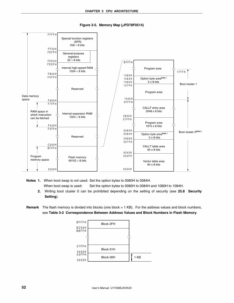
CHAPTER 3 CPU ARCHITECTURE
User’s Manual U17336EJ5V0UD 52
Figure 3-5. Memory Map (μPD78F0514)
Special function registers (SFR)
256 × 8 bits
Internal high-speed RAM1024 × 8 bits
Internal expansion RAM1024 × 8 bits
Reserved
General-purpose registers 32 × 8 bits
Reserved
F F F F H
F F 0 0 HF E F F H
F E E 0 HF E D F H
F B 0 0 HF A F F H
F 8 0 0 HF 7 F F H
F 4 0 0 HF 3 F F H
C 0 0 0 HB F F F H
0 0 0 0 H
Program memory space
RAM space inwhich instructioncan be fetched
Data memoryspace
Flash memory49152 × 8 bits Vector table area
64 x 8 bits
CALLT table area64 x 8 bits
Program area1915 x 8 bits
Option byte areaNote 1
5 x 8 bits
CALLF entry area2048 x 8 bits
Program area
Program area
Option byte areaNote 1
5 x 8 bits
Boot cluster 0Note 2
Boot cluster 1
0 0 4 0 H0 0 3 F H
0 0 0 0 H
0 0 8 0 H0 0 7 F H
0 8 0 0 H0 7 F F H
1 0 0 0 H0 F F F H
1 0 8 5 H1 0 8 4 H1 0 8 0 H1 0 7 F H
0 0 8 5 H0 0 8 4 H
B F F F H
1 F F F H
Notes 1. When boot swap is not used: Set the option bytes to 0080H to 0084H.
When boot swap is used: Set the option bytes to 0080H to 0084H and 1080H to 1084H.
2. Writing boot cluster 0 can be prohibited depending on the setting of security (see 25.8 Security
Setting).
Remark The flash memory is divided into blocks (one block = 1 KB). For the address values and block numbers,
see Table 3-2 Correspondence Between Address Values and Block Numbers in Flash Memory.
Block 00H
Block 01H
Block 2FH
1 KB
B F F F H
0 7 F F H
0 0 0 0 H
0 4 0 0 H0 3 F F H
B C 0 0 HB B F F H

CHAPTER 3 CPU ARCHITECTURE
User’s Manual U17336EJ5V0UD 53
Figure 3-6. Memory Map (μPD78F0515)
Special function registers (SFR)
256 × 8 bits
Internal high-speed RAM1024 × 8 bits
Internal expansion RAM2048 × 8 bits
General-purpose registers 32 × 8 bits
Reserved
Flash memory61440 × 8 bits
F F F F H
F F 0 0 HF E F F H
F E E 0 HF E D F H
F B 0 0 HF A F F H
F 8 0 0 HF 7 F F H
F 0 0 0 HE F F F H
0 0 0 0 H
Program memory space
RAM space inwhich instructioncan be fetched
Data memoryspace
Vector table area64 x 8 bits
CALLT table area64 x 8 bits
Program area1915 x 8 bits
Option byte areaNote 1
5 x 8 bits
CALLF entry area2048 x 8 bits
Program area
Program area
Option byte areaNote 1
5 x 8 bits
Boot cluster 0Note 2
Boot cluster 1
0 0 4 0 H0 0 3 F H
0 0 0 0 H
0 0 8 0 H0 0 7 F H
0 8 0 0 H0 7 F F H
1 0 0 0 H0 F F F H
1 0 8 5 H1 0 8 4 H1 0 8 0 H1 0 7 F H
0 0 8 5 H0 0 8 4 H
E F F F H
1 F F F H
Notes 1. When boot swap is not used: Set the option bytes to 0080H to 0084H.
When boot swap is used: Set the option bytes to 0080H to 0084H and 1080H to 1084H.
2. Writing boot cluster 0 can be prohibited depending on the setting of security (see 25.8 Security
Setting).
Remark The flash memory is divided into blocks (one block = 1 KB). For the address values and block numbers,
see Table 3-2 Correspondence Between Address Values and Block Numbers in Flash Memory.
Block 00H
Block 01H
Block 3BH
1 KB
E F F F H
0 7 F F H
0 0 0 0 H
0 4 0 0 H0 3 F F H
E C 0 0 HE B F F H

CHAPTER 3 CPU ARCHITECTURE
User’s Manual U17336EJ5V0UD 54
Figure 3-7. Memory Map (μPD78F0515D)
F F F F H
F F 0 0 HF E F F H
F E E 0 HF E D F H
F B 0 0 HF A F F H
F 8 0 0 HF 7 F F H
F 0 0 0 HE F F F H
0 0 0 0 H
Program memory space
RAM space inwhich instructioncan be fetched
Data memoryspace
Special function registers (SFR)
256 × 8 bits
Internal high-speed RAM1024 × 8 bits
Internal expansion RAM2048 × 8 bits
General-purpose registers 32 × 8 bits
Reserved
Flash memory61440 × 8 bits
Vector table area64 x 8 bits
CALLT table area64 x 8 bits
Program area1905 x 8 bits
Option byte areaNote 1
5 x 8 bits
CALLF entry area2048 x 8 bits
Program area
Program area
Option byte areaNote 1
5 x 8 bits
Boot cluster 0Note 2
Boot cluster 1
0 0 4 0 H0 0 3 F H
0 0 0 0 H
0 0 8 0 H0 0 7 F H
0 8 0 0 H0 7 F F H
1 0 0 0 H0 F F F H
1 0 8 5 H1 0 8 4 H1 0 8 0 H1 0 7 F H
0 0 8 5 H0 0 8 4 H
E F F F H
1 F F F H1 0 8 F H1 0 8 E H
0 0 8 F H0 0 8 E H
On-chip debug securityID setting areaNote 1
10 x 8 bits
On-chip debug securityID setting areaNote1
10 x 8 bits
Notes 1. When boot swap is not used: Set the option bytes to 0080H to 0084H, and the on-chip debug security
IDs to 0085H to 008EH.
When boot swap is used: Set the option bytes to 0080H to 0084H and 1080H to 1084H, and the
on-chip debug security IDs to 0085H to 008EH and 1085H to 108EH.
2. Writing boot cluster 0 can be prohibited depending on the setting of security (see 25.8 Security
Setting).
Remark The flash memory is divided into blocks (one block = 1 KB). For the address values and block numbers,
see Table 3-2 Correspondence Between Address Values and Block Numbers in Flash Memory.
Block 00H
Block 01H
Block 3BH
1 KB
E F F F H
0 7 F F H
0 0 0 0 H
0 4 0 0 H0 3 F F H
E C 0 0 HE B F F H
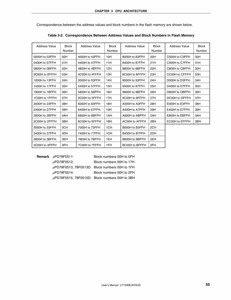
CHAPTER 3 CPU ARCHITECTURE
User’s Manual U17336EJ5V0UD 55
Correspondence between the address values and block numbers in the flash memory are shown below.
Table 3-2. Correspondence Between Address Values and Block Numbers in Flash Memory
Address Value Block
Number
Address Value Block
Number
Address Value Block
Number
Address Value Block
Number
0000H to 03FFH 00H 4000H to 43FFH 10H 8000H to 83FFH 20H C000H to C3FFH 30H
0400H to 07FFH 01H 4400H to 47FFH 11H 8400H to 87FFH 21H C400H to C7FFH 31H
0800H to 0BFFH 02H 4800H to 4BFFH 12H 8800H to 8BFFH 22H C800H to CBFFH 32H
0C00H to 0FFFH 03H 4C00H to 4FFFH 13H 8C00H to 8FFFH 23H CC00H to CFFFH 33H
1000H to 13FFH 04H 5000H to 53FFH 14H 9000H to 93FFH 24H D000H to D3FFH 34H
1400H to 17FFH 05H 5400H to 57FFH 15H 9400H to 97FFH 25H D400H to D7FFH 35H
1800H to 1BFFH 06H 5800H to 5BFFH 16H 9800H to 9BFFH 26H D800H to DBFFH 36H
1C00H to 1FFFH 07H 5C00H to 5FFFH 17H 9C00H to 9FFFH 27H DC00H to DFFFH 37H
2000H to 23FFH 08H 6000H to 63FFH 18H A000H to A3FFH 28H E000H to E3FFH 38H
2400H to 27FFH 09H 6400H to 67FFH 19H A400H to A7FFH 29H E400H to E7FFH 39H
2800H to 2BFFH 0AH 6800H to 6BFFH 1AH A800H to ABFFH 2AH E800H to EBFFH 3AH
2C00H to 2FFFH 0BH 6C00H to 6FFFH 1BH AC00H to AFFFH 2BH EC00H to EFFFH 3BH
3000H to 33FFH 0CH 7000H to 73FFH 1CH B000H to B3FFH 2CH
3400H to 37FFH 0DH 7400H to 77FFH 1DH B400H to B7FFH 2DH
3800H to 3BFFH 0EH 7800H to 7BFFH 1EH B800H to BBFFH 2EH
3C00H to 3FFFH 0FH 7C00H to 7FFFH 1FH BC00H to BFFFH 2FH
Remark μPD78F0511: Block numbers 00H to 0FH
μPD78F0512: Block numbers 00H to 17H
μPD78F0513, 78F0513D: Block numbers 00H to 1FH
μPD78F0514: Block numbers 00H to 2FH
μPD78F0515, 78F0515D: Block numbers 00H to 3BH

CHAPTER 3 CPU ARCHITECTURE
User’s Manual U17336EJ5V0UD 56
3.1.1 Internal program memory space
The internal program memory space stores the program and table data. Normally, it is addressed with the program
counter (PC).
78K0/KC2 products incorporate internal ROM (flash memory), as shown below.
Table 3-3. Internal ROM Capacity
Internal ROM Part Number
Structure Capacity
μPD78F0511 16384 × 8 bits (0000H to 3FFFH)
μPD78F0512 24576 × 8 bits (0000H to 5FFFH)
μPD78F0513, 78F0513D 32768 × 8 bits (0000H to 7FFFH)
μPD78F0514 49152 × 8 bits (0000H to BFFFH)
μPD78F0515, 78F0515D
Flash memory
61440 × 8 bits (0000H to EFFFH)
The internal program memory space is divided into the following areas.
(1) Vector table area
The 64-byte area 0000H to 003FH is reserved as a vector table area. The program start addresses for branch
upon reset or generation of each interrupt request are stored in the vector table area.
Of the 16-bit address, the lower 8 bits are stored at even addresses and the higher 8 bits are stored at odd
addresses.
Table 3-4. Vector Table
Vector Table Address Interrupt Source Vector Table Address Interrupt Source
0000H RESET input, POC, LVI, WDT 001CH INTTMH0
0004H INTLVI 001EH INTTM50
0006H INTP0 0020H INTTM000
0008H INTP1 0022H INTTM010
000AH INTP2 0024H INTAD
000CH INTP3 0026H INTSR0
000EH INTP4 0028H INTWTI
0010H INTP5 002AH INTTM51
0012H INTSRE6 002CH INTKR
0014H INTSR6 002EH INTWT
0016H INTST6 0030H INTP6Note 1
0018H INTCSI10/INTST0 0034H INTIIC0/INTDMUNote 2
001AH INTTMH1 003EH BRK
Notes 1. Available only in the 48-pin products.
2. Available only in the μPD78F0514, 78F0515, and 78F0515D.
CHAPTER 3 CPU ARCHITECTURE
User’s Manual U17336EJ5V0UD 57
(2) CALLT instruction table area
The 64-byte area 0040H to 007FH can store the subroutine entry address of a 1-byte call instruction (CALLT).
(3) Option byte area
A 5-byte area of 0080H to 0084H and 1080H to 1084H can be used as an option byte area. Set the option byte
at 0080H to 0084H when the boot swap is not used, and at 0080H to 0084H and 1080H to 1084H when the boot
swap is used. For details, see CHAPTER 24 OPTION BYTE.
(4) CALLF instruction entry area
The area 0800H to 0FFFH can perform a direct subroutine call with a 2-byte call instruction (CALLF).
(5) On-chip debug security ID setting area (μPD78F0513D and 78F0515D only)
A 10-byte area of 0085H to 008EH and 1085H to 108EH can be used as an on-chip debug security ID setting
area. Set the on-chip debug security ID of 10 bytes at 0085H to 008EH when the boot swap is not used and at
0085H to 008EH and 1085H to 108EH when the boot swap is used. For details, see CHAPTER 26 ON-CHIP
DEBUG FUNCTION (μPD78F0513D AND 78F0515D ONLY).

CHAPTER 3 CPU ARCHITECTURE
User’s Manual U17336EJ5V0UD 58
3.1.2 Internal data memory space
78K0/KC2 products incorporate the following RAMs.
(1) Internal high-speed RAM
Table 3-5. Internal High-Speed RAM Capacity
Part Number Internal High-Speed RAM
μPD78F0511 768 × 8 bits (FC00H to FEFFH)
μPD78F0512
μPD78F0513, 78F0513D
μPD78F0514
μPD78F0515, 78F0515D
1024 × 8 bits (FB00H to FEFFH)
The 32-byte area FEE0H to FEFFH is assigned to four general-purpose register banks consisting of eight 8-bit
registers per bank.
This area cannot be used as a program area in which instructions are written and executed.
The internal high-speed RAM can also be used as a stack memory.
(2) Internal expansion RAM
Table 3-6. Internal Expansion RAM Capacity
Part Number Internal Expansion RAM
μPD78F0511
μPD78F0512
μPD78F0513, 78F0513D
−
μPD78F0514 1024 × 8 bits (F400H to F7FFH)
μPD78F0515, 78F0515D 2048 × 8 bits (F000H to F7FFH)
The internal expansion RAM can also be used as a normal data area similar to the internal high-speed RAM, as
well as a program area in which instructions can be written and executed.
The internal expansion RAM cannot be used as a stack memory.

CHAPTER 3 CPU ARCHITECTURE
User’s Manual U17336EJ5V0UD 59
3.1.3 Special function register (SFR) area
On-chip peripheral hardware special function registers (SFRs) are allocated in the area FF00H to FFFFH (see
Table 3-7 Special Function Register List in 3.2.3 Special function registers (SFRs)).
Caution Do not access addresses to which SFRs are not assigned.
3.1.4 Data memory addressing
Addressing refers to the method of specifying the address of the instruction to be executed next or the address of
the register or memory relevant to the execution of instructions.
Several addressing modes are provided for addressing the memory relevant to the execution of instructions for the
78K0/KC2, based on operability and other considerations. For areas containing data memory in particular, special
addressing methods designed for the functions of special function registers (SFR) and general-purpose registers are
available for use. Figures 3-8 to 3-14 show correspondence between data memory and addressing. For details of
each addressing mode, see 3.4 Operand Address Addressing.

CHAPTER 3 CPU ARCHITECTURE
User’s Manual U17336EJ5V0UD 60
Figure 3-8. Correspondence Between Data Memory and Addressing (μPD78F0511)
Special function registers (SFR)256 × 8 bits
Short direct addressing
SFR addressing
F F F F H
F F 2 0 HF F 1 F H
0 0 0 0 H
F F 0 0 HF E F F H
F E E 0 HF E D F H
F E 2 0 HF E 1 F H
F C 0 0 HF B F F H
4 0 0 0 H3 F F F H
Internal high-speed RAM768 × 8 bits
General-purpose registers32 × 8 bits
Reserved
Flash memory16384 × 8 bits
Register addressing
Direct addressing
Register indirect addressing
Based addressing
Based indexed addressing

CHAPTER 3 CPU ARCHITECTURE
User’s Manual U17336EJ5V0UD 61
Figure 3-9. Correspondence Between Data Memory and Addressing (μPD78F0512)
Special function registers (SFR)256 × 8 bits
Short direct addressing
SFR addressing
F F F F H
F F 2 0 HF F 1 F H
0 0 0 0 H
F F 0 0 HF E F F H
F E E 0 HF E D F H
F E 2 0 HF E 1 F H
F B 0 0 HF A F F H
6 0 0 0 H5 F F F H
Internal high-speed RAM1024 × 8 bits
General-purpose registers32 × 8 bits
Reserved
Flash memory24576 × 8 bits
Register addressing
Direct addressing
Register indirect addressing
Based addressing
Based indexed addressing

CHAPTER 3 CPU ARCHITECTURE
User’s Manual U17336EJ5V0UD 62
Figure 3-10. Correspondence Between Data Memory and Addressing (μPD78F0513 and 78F0513D)
Special function registers (SFR)256 × 8 bits
Short direct addressing
SFR addressing
F F F F H
F F 2 0 HF F 1 F H
0 0 0 0 H
F F 0 0 HF E F F H
F E E 0 HF E D F H
F E 2 0 HF E 1 F H
F B 0 0 HF A F F H
8 0 0 0 H7 F F F H
Internal high-speed RAM1024 × 8 bits
General-purpose registers32 × 8 bits
Reserved
Flash memory32768 × 8 bits
Register addressing
Direct addressing
Register indirect addressing
Based addressing
Based indexed addressing

CHAPTER 3 CPU ARCHITECTURE
User’s Manual U17336EJ5V0UD 63
Figure 3-11 . Correspondence Between Data Memory and Addressing (μPD78F0514)
Special function registers (SFR)256 × 8 bits
Short direct addressing
SFR addressing
F F F F H
F F 2 0 HF F 1 F H
0 0 0 0 H
F F 0 0 HF E F F H
F E E 0 HF E D F H
F E 2 0 HF E 1 F H
C 0 0 0 HB F F F H
Internal high-speed RAM1024 × 8 bits
General-purpose registers32 × 8 bits
Reserved
Flash memory49152 × 8 bits
Register addressing
Direct addressing
Register indirect addressing
Based addressing
Based indexed addressing
F 8 0 0 HF 7 F F H
F 4 0 0 HF 3 F F H
F B 0 0 HF A F F H
Internal expansion RAM1024 × 8 bits
Reserved

CHAPTER 3 CPU ARCHITECTURE
User’s Manual U17336EJ5V0UD 64
Figure 3-12. Correspondence Between Data Memory and Addressing (μPD78F0515 and 78F0515D)
Special function registers (SFR)256 × 8 bits
Short direct addressing
SFR addressing
F F F F H
F F 2 0 HF F 1 F H
0 0 0 0 H
F F 0 0 HF E F F H
F E E 0 HF E D F H
F E 2 0 HF E 1 F H
F 0 0 0 HE F F F H
Internal high-speed RAM1024 × 8 bits
General-purpose registers32 × 8 bits
Reserved
Flash memory61440 × 8 bits
Register addressing
Direct addressing
Register indirect addressing
Based addressing
Based indexed addressing
F 8 0 0 HF 7 F F H
F B 0 0 HF A F F H
Internal expansion RAM2048 × 8 bits

CHAPTER 3 CPU ARCHITECTURE
User’s Manual U17336EJ5V0UD 65
3.2 Processor Registers
The 78K0/KC2 products incorporate the following processor registers.
3.2.1 Control registers
The control registers control the program sequence, statuses and stack memory. The control registers consist of a
program counter (PC), a program status word (PSW) and a stack pointer (SP).
(1) Program counter (PC)
The program counter is a 16-bit register that holds the address information of the next program to be executed.
In normal operation, PC is automatically incremented according to the number of bytes of the instruction to be
fetched. When a branch instruction is executed, immediate data and register contents are set.
Reset signal generation sets the reset vector table values at addresses 0000H and 0001H to the program counter.
Figure 3-13. Format of Program Counter
15
PC PC15 PC14 PC13 PC12 PC11 PC10 PC9 PC8 PC7 PC6 PC5 PC4 PC3 PC2 PC1 PC0
0
(2) Program status word (PSW)
The program status word is an 8-bit register consisting of various flags set/reset by instruction execution.
Program status word contents are stored in the stack area upon interrupt request generation or PUSH PSW
instruction execution and are restored upon execution of the RETB, RETI and POP PSW instructions.
Reset signal generation sets PSW to 02H.
Figure 3-14. Format of Program Status Word
IE Z RBS1 AC RBS0 ISP CY
7 0
0PSW
(a) Interrupt enable flag (IE)
This flag controls the interrupt request acknowledge operations of the CPU.
When 0, the IE flag is set to the interrupt disabled (DI) state, and all maskable interrupt requests are disabled.
When 1, the IE flag is set to the interrupt enabled (EI) state and interrupt request acknowledgment is
controlled with an in-service priority flag (ISP), an interrupt mask flag for various interrupt sources, and a
priority specification flag.
The IE flag is reset (0) upon DI instruction execution or interrupt acknowledgment and is set (1) upon EI
instruction execution.


CHAPTER 3 CPU ARCHITECTURE
User’s Manual U17336EJ5V0UD 67
Figure 3-16. Data to Be Saved to Stack Memory
(a) PUSH rp instruction (when SP = FEE0H)
Register pair lower
FEE0HSP
SP
FEE0H
FEDFH
FEDEH
Register pair higher
FEDEH
(b) CALL, CALLF, CALLT instructions (when SP = FEE0H)
PC15 to PC8
FEE0HSP
SP
FEE0H
FEDFH
FEDEH PC7 to PC0FEDEH
(c) Interrupt, BRK instructions (when SP = FEE0H)
PC15 to PC8
PSWFEDFH
FEE0HSP
SP
FEE0H
FEDEH
FEDDH PC7 to PC0FEDDH
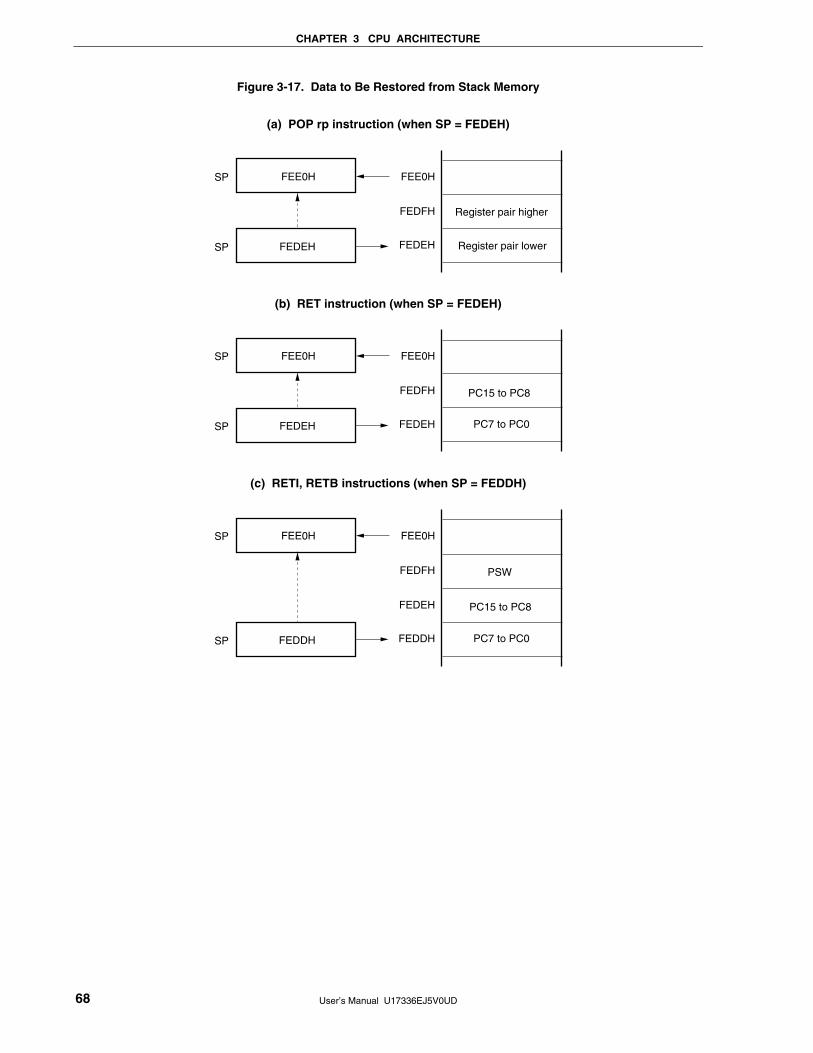
CHAPTER 3 CPU ARCHITECTURE
User’s Manual U17336EJ5V0UD 68
Figure 3-17. Data to Be Restored from Stack Memory
(a) POP rp instruction (when SP = FEDEH)
Register pair lower
FEE0HSP
SP
FEE0H
FEDFH
FEDEH
Register pair higher
FEDEH
(b) RET instruction (when SP = FEDEH)
PC15 to PC8
FEE0HSP
SP
FEE0H
FEDFH
FEDEH PC7 to PC0FEDEH
(c) RETI, RETB instructions (when SP = FEDDH)
PC15 to PC8
PSWFEDFH
FEE0HSP
SP
FEE0H
FEDEH
FEDDH PC7 to PC0FEDDH

CHAPTER 3 CPU ARCHITECTURE
User’s Manual U17336EJ5V0UD 69
3.2.2 General-purpose registers
General-purpose registers are mapped at particular addresses (FEE0H to FEFFH) of the data memory. The
general-purpose registers consists of 4 banks, each bank consisting of eight 8-bit registers (X, A, C, B, E, D, L, and H).
Each register can be used as an 8-bit register, and two 8-bit registers can also be used in a pair as a 16-bit register
(AX, BC, DE, and HL).
These registers can be described in terms of function names (X, A, C, B, E, D, L, H, AX, BC, DE, and HL) and
absolute names (R0 to R7 and RP0 to RP3).
Register banks to be used for instruction execution are set by the CPU control instruction (SEL RBn). Because of
the 4-register bank configuration, an efficient program can be created by switching between a register for normal
processing and a register for interrupts for each bank.
Figure 3-18. Configuration of General-Purpose Registers
(a) Function name
Register bank 0
Register bank 1
Register bank 2
Register bank 3
FEFFH
FEF8H
FEE0H
HL
DE
BC
AX
H
15 0 7 0
L
D
E
B
C
A
X
16-bit processing 8-bit processing
FEF0H
FEE8H
(b) Absolute name
Register bank 0
Register bank 1
Register bank 2
Register bank 3
FEFFH
FEF8H
FEE0H
RP3
RP2
RP1
RP0
R7
15 0 7 0
R6
R5
R4
R3
R2
R1
R0
16-bit processing 8-bit processing
FEF0H
FEE8H

CHAPTER 3 CPU ARCHITECTURE
User’s Manual U17336EJ5V0UD 70
3.2.3 Special function registers (SFRs)
Unlike a general-purpose register, each special function register has a special function.
SFRs are allocated to the FF00H to FFFFH area.
Special function registers can be manipulated like general-purpose registers, using operation, transfer, and bit
manipulation instructions. The manipulatable bit units, 1, 8, and 16, depend on the special function register type.
Each manipulation bit unit can be specified as follows.
• 1-bit manipulation
Describe the symbol reserved by the assembler for the 1-bit manipulation instruction operand (sfr.bit).
This manipulation can also be specified with an address.
• 8-bit manipulation
Describe the symbol reserved by the assembler for the 8-bit manipulation instruction operand (sfr).
This manipulation can also be specified with an address.
• 16-bit manipulation
Describe the symbol reserved by the assembler for the 16-bit manipulation instruction operand (sfrp).
When specifying an address, describe an even address.
Table 3-7 gives a list of the special function registers. The meanings of items in the table are as follows.
• Symbol
Symbol indicating the address of a special function register. It is a reserved word in the RA78K0, and is defined
as an sfr variable using the #pragma sfr directive in the CC78K0. When using the RA78K0, ID78K0-QB, and
SM+ for 78K0/KX2, symbols can be written as an instruction operand.
• R/W
Indicates whether the corresponding special function register can be read or written.
R/W: Read/write enable
R: Read only
W: Write only
• Manipulatable bit units
Indicates the manipulatable bit unit (1, 8, or 16). “−” indicates a bit unit for which manipulation is not possible.
• After reset
Indicates each register status upon reset signal generation.

CHAPTER 3 CPU ARCHITECTURE
User’s Manual U17336EJ5V0UD 71
Table 3-7. Special Function Register List (1/4)
Manipulatable Bit Unit Address Special Function Register (SFR) Name Symbol R/W
1 Bit 8 Bits 16 Bits
After
Reset
FF00H Port register 0 P0 R/W √ √ − 00H
FF01H Port register 1 P1 R/W √ √ − 00H
FF02H Port register 2 P2 R/W √ √ − 00H
FF03H Port register 3 P3 R/W √ √ − 00H
FF04H Port register 4 P4 R/W √ √ − 00H
FF06H Port register 6 P6 R/W √ √ − 00H
FF07H Port register 7 P7 R/W √ √ − 00H
FF08H 10-bit A/D conversion result register ADCR R − − √ 0000H
FF09H 8-bit A/D conversion result register ADCRH R − √ − 00H
FF0AH Receive buffer register 6 RXB6 R − √ − FFH
FF0BH Transmit buffer register 6 TXB6 R/W − √ − FFH
FF0CH Port register 12 P12 R/W √ √ − 00H
FF0DH Port register 13Note P13 R/W √ √ − 00H
FF0EH Port register 14Note P14 R/W √ √ − 00H
FF0FH Serial I/O shift register 10 SIO10 R − √ − 00H
FF10H
FF11H
16-bit timer counter 00 TM00 R − − √ 0000H
FF12H
FF13H
16-bit timer capture/compare register 000 CR000 R/W − − √ 0000H
FF14H
FF15H
16-bit timer capture/compare register 010 CR010 R/W − − √ 0000H
FF16H 8-bit timer counter 50 TM50 R − √ − 00H
FF17H 8-bit timer compare register 50 CR50 R/W − √ − 00H
FF18H 8-bit timer H compare register 00 CMP00 R/W − √ − 00H
FF19H 8-bit timer H compare register 10 CMP10 R/W − √ − 00H
FF1AH 8-bit timer H compare register 01 CMP01 R/W − √ − 00H
FF1BH 8-bit timer H compare register 11 CMP11 R/W − √ − 00H
FF1FH 8-bit timer counter 51 TM51 R − √ − 00H
FF20H Port mode register 0 PM0 R/W √ √ − FFH
FF21H Port mode register 1 PM1 R/W √ √ − FFH
FF22H Port mode register 2 PM2 R/W √ √ − FFH
FF23H Port mode register 3 PM3 R/W √ √ − FFH
FF24H Port mode register 4 PM4 R/W √ √ − FFH
FF26H Port mode register 6 PM6 R/W √ √ − FFH
FF27H Port mode register 7 PM7 R/W √ √ − FFH
FF28H A/D converter mode register ADM R/W √ √ − 00H
FF29H Analog input channel specification register ADS R/W √ √ − 00H
FF2CH Port mode register 12 PM12 R/W √ √ − FFH
FF2EH Port mode register 14Note PM14 R/W √ √ − FFH
FF2FH A/D port configuration register ADPC R/W √ √ − 00H
Note Available only in the 48-pin products.
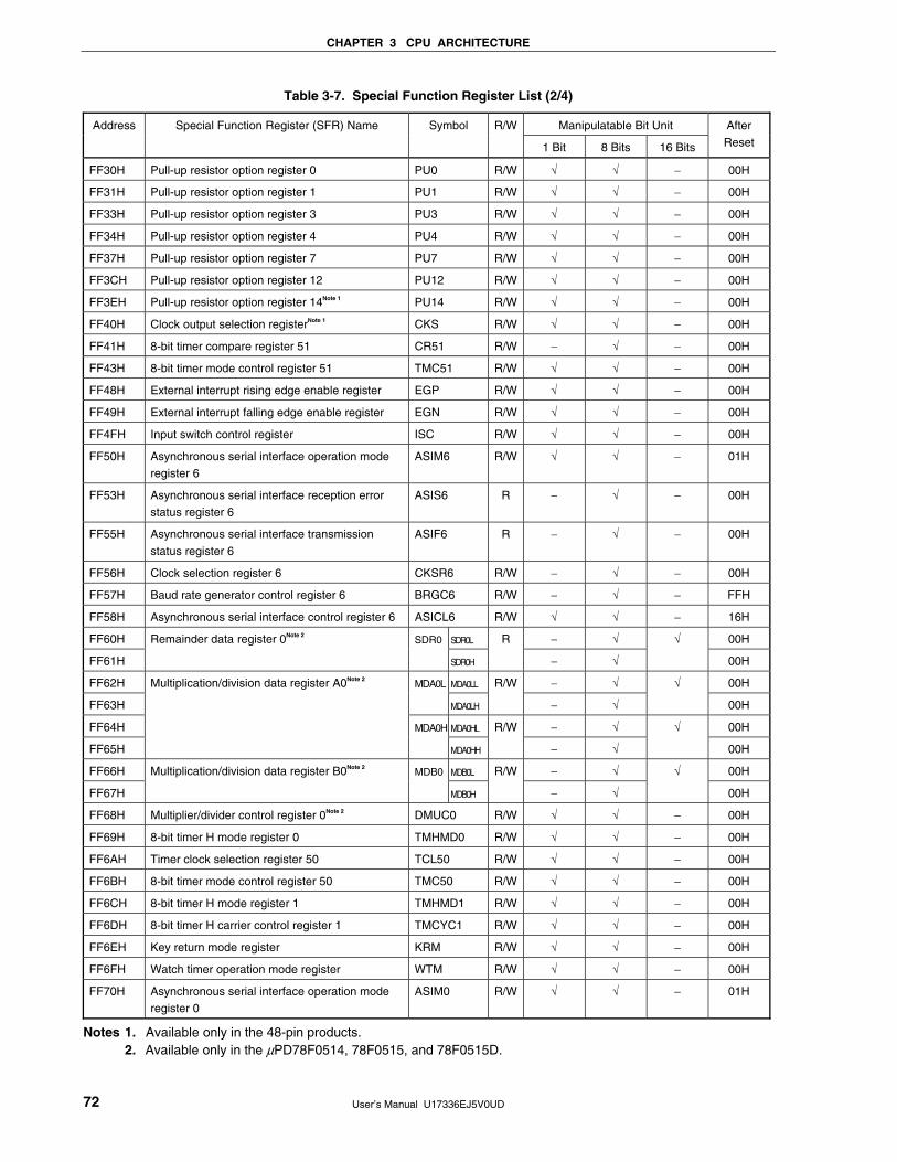
CHAPTER 3 CPU ARCHITECTURE
User’s Manual U17336EJ5V0UD 72
Table 3-7. Special Function Register List (2/4)
Manipulatable Bit Unit Address Special Function Register (SFR) Name Symbol R/W
1 Bit 8 Bits 16 Bits
After
Reset
FF30H Pull-up resistor option register 0 PU0 R/W √ √ − 00H
FF31H Pull-up resistor option register 1 PU1 R/W √ √ − 00H
FF33H Pull-up resistor option register 3 PU3 R/W √ √ − 00H
FF34H Pull-up resistor option register 4 PU4 R/W √ √ − 00H
FF37H Pull-up resistor option register 7 PU7 R/W √ √ − 00H
FF3CH Pull-up resistor option register 12 PU12 R/W √ √ − 00H
FF3EH Pull-up resistor option register 14Note 1 PU14 R/W √ √ − 00H
FF40H Clock output selection registerNote 1 CKS R/W √ √ − 00H
FF41H 8-bit timer compare register 51 CR51 R/W − √ − 00H
FF43H 8-bit timer mode control register 51 TMC51 R/W √ √ − 00H
FF48H External interrupt rising edge enable register EGP R/W √ √ − 00H
FF49H External interrupt falling edge enable register EGN R/W √ √ − 00H
FF4FH Input switch control register ISC R/W √ √ − 00H
FF50H Asynchronous serial interface operation mode register 6
ASIM6 R/W √ √ − 01H
FF53H Asynchronous serial interface reception error status register 6
ASIS6 R − √ − 00H
FF55H Asynchronous serial interface transmission
status register 6
ASIF6 R − √ − 00H
FF56H Clock selection register 6 CKSR6 R/W − √ − 00H
FF57H Baud rate generator control register 6 BRGC6 R/W − √ − FFH
FF58H Asynchronous serial interface control register 6 ASICL6 R/W √ √ − 16H
FF60H SDR0L − √ 00H
FF61H
Remainder data register 0Note 2 SDR0
SDR0H
R
− √
√
00H
FF62H MDA0LL − √ 00H
FF63H
MDA0L
MDA0LH
R/W
− √
√
00H
FF64H MDA0HL − √ 00H
FF65H
Multiplication/division data register A0Note 2
MDA0H
MDA0HH
R/W
− √
√
00H
FF66H MDB0L − √ 00H
FF67H
Multiplication/division data register B0Note 2 MDB0
MDB0H
R/W
− √
√
00H
FF68H Multiplier/divider control register 0Note 2 DMUC0 R/W √ √ − 00H
FF69H 8-bit timer H mode register 0 TMHMD0 R/W √ √ − 00H
FF6AH Timer clock selection register 50 TCL50 R/W √ √ − 00H
FF6BH 8-bit timer mode control register 50 TMC50 R/W √ √ − 00H
FF6CH 8-bit timer H mode register 1 TMHMD1 R/W √ √ − 00H
FF6DH 8-bit timer H carrier control register 1 TMCYC1 R/W √ √ − 00H
FF6EH Key return mode register KRM R/W √ √ − 00H
FF6FH Watch timer operation mode register WTM R/W √ √ − 00H
FF70H Asynchronous serial interface operation mode register 0
ASIM0 R/W √ √ − 01H
Notes 1. Available only in the 48-pin products. 2. Available only in the μPD78F0514, 78F0515, and 78F0515D.

CHAPTER 3 CPU ARCHITECTURE
User’s Manual U17336EJ5V0UD 73
Table 3-7. Special Function Register List (3/4)
Manipulatable Bit Unit Address Special Function Register (SFR) Name Symbol R/W
1 Bit 8 Bits 16 Bits
After
Reset
FF71H Baud rate generator control register 0 BRGC0 R/W − √ − 1FH
FF72H Receive buffer register 0 RXB0 R − √ − FFH
FF73H Asynchronous serial interface reception error status register 0
ASIS0 R − √ − 00H
FF74H Transmit shift register 0 TXS0 W − √ − FFH
FF80H Serial operation mode register 10 CSIM10 R/W √ √ − 00H
FF81H Serial clock selection register 10 CSIC10 R/W √ √ − 00H
FF84H Transmit buffer register 10 SOTB10 R/W − √ − 00H
FF8CH Timer clock selection register 51 TCL51 R/W √ √ − 00H
FF99H Watchdog timer enable register WDTE R/W − √ − Note 1
1AH/9AH
FF9FH Clock operation mode select register OSCCTL R/W √ √ − 00H
FFA0H Internal oscillation mode register RCM R/W √ √ − 80HNote 2
FFA1H Main clock mode register MCM R/W √ √ − 00H
FFA2H Main OSC control register MOC R/W √ √ − 80H
FFA3H Oscillation stabilization time counter status register OSTC R √ √ − 00H
FFA4H Oscillation stabilization time select register OSTS R/W − √ − 05H
FFA5H IIC shift register 0 IIC0 R/W − √ − 00H
FFA6H IIC control register 0 IICC0 R/W √ √ − 00H
FFA7H Slave address register 0 SVA0 R/W − √ − 00H
FFA8H IIC clock selection register 0 IICCL0 R/W √ √ − 00H
FFA9H IIC function expansion register 0 IICX0 R/W √ √ − 00H
FFAAH IIC status register 0 IICS0 R √ √ − 00H
FFABH IIC flag register 0 IICF0 R/W √ √ − 00H
FFACH Reset control flag register RESF R − √ − 00HNote 3
FFBAH 16-bit timer mode control register 00 TMC00 R/W √ √ − 00H
FFBBH Prescaler mode register 00 PRM00 R/W √ √ − 00H
FFBCH Capture/compare control register 00 CRC00 R/W √ √ − 00H
FFBDH 16-bit timer output control register 00 TOC00 R/W √ √ − 00H
FFBEH Low-voltage detection register LVIM R/W √ √ − 00HNote 3
FFBFH Low-voltage detection level selection register LVIS R/W √ √ − 00HNote 3
FFE0H Interrupt request flag register 0L IF0 IF0L R/W √ √ 00H
FFE1H Interrupt request flag register 0H IF0H R/W √ √
√
00H
FFE2H Interrupt request flag register 1L IF1 IF1L R/W √ √ 00H
FFE3H Interrupt request flag register 1H IF1H R/W √ √
√
00H
FFE4H Interrupt mask flag register 0L MK0 MK0L R/W √ √ FFH
FFE5H Interrupt mask flag register 0H MK0H R/W √ √
√
FFH
Notes 1. The reset value of WDTE is determined by setting of option byte.
2. The value of this register is 00H immediately after a reset release but automatically changes to 80H after
oscillation accuracy stabilization of high-speed internal oscillator has been waited.
3. The reset values of RESF, LVIM, and LVIS vary depending on the reset source.

CHAPTER 3 CPU ARCHITECTURE
User’s Manual U17336EJ5V0UD 74
Table 3-7. Special Function Register List (4/4)
Manipulatable Bit Unit Address Special Function Register (SFR) Name Symbol R/W
1 Bit 8 Bits 16 Bits
After
Reset
FFE6H Interrupt mask flag register 1L MK1 MK1L R/W √ √ FFH
FFE7H Interrupt mask flag register 1H MK1H R/W √ √
√
FFH
FFE8H Priority specification flag register 0L PR0 PR0L R/W √ √ FFH
FFE9H Priority specification flag register 0H PR0H R/W √ √
√
FFH
FFEAH Priority specification flag register 1L PR1 PR1L R/W √ √ FFH
FFEBH Priority specification flag register 1H PR1H R/W √ √
√
FFH
FFF0H Internal memory size switching registerNote 1 IMS R/W − √ − CFH
FFF4H Internal expansion RAM size switching registerNote 1
IXS R/W − √ − 0CH
FFFBH Processor clock control register PCC R/W √ √ − 01H
Notes 1. Regardless of the internal memory capacity, the initial values of the internal memory size switching register
(IMS) and internal expansion RAM size switching register (IXS) of all products in the 78K0/KC2 are fixed
(IMS = CFH, IXS = 0CH). Therefore, set the value corresponding to each product as indicated below.
Flash Memory Version
(78K0/KC2)
IMS IXS ROM
Capacity
Internal High-Speed
RAM Capacity
Internal Expansion
RAM Capacity
μPD78F0511 04H 16 KB 768 bytes
μPD78F0512 C6H 24 KB
μPD78F0513, 78F0513DNote 2 C8H
0CH
32 KB
−
μPD78F0514 CCH 0AH 48 KB 1 KB
μPD78F0515, 78F0515DNote 2 CFH 08H 60 KB
1 KB
2 KB
2. The ROM and RAM capacities of the products with the on-chip debug function can be debugged by setting
IMS and IXS, according to the debug target products. Set IMS and IXS according to the debug target
products.
<R>

CHAPTER 3 CPU ARCHITECTURE
User’s Manual U17336EJ5V0UD 75
3.3 Instruction Address Addressing
An instruction address is determined by contents of the program counter (PC), and is normally incremented (+1 for
each byte) automatically according to the number of bytes of an instruction to be fetched each time another instruction
is executed. When a branch instruction is executed, the branch destination information is set to PC and branched by
the following addressing (for details of instructions, refer to the 78K/0 Series Instructions User’s Manual (U12326E)).
3.3.1 Relative addressing
[Function]
The value obtained by adding 8-bit immediate data (displacement value: jdisp8) of an instruction code to the
start address of the following instruction is transferred to the program counter (PC) and branched. The
displacement value is treated as signed two’s complement data (−128 to +127) and bit 7 becomes a sign bit.
In other words, relative addressing consists of relative branching from the start address of the following
instruction to the −128 to +127 range.
This function is carried out when the BR $addr16 instruction or a conditional branch instruction is executed.
[Illustration]
15 0
PC
+
15 08 7 6
S
15 0
PC
α
jdisp8
When S = 0, all bits of are 0.When S = 1, all bits of are 1.
PC indicates the start addressof the instruction after the BR instruction.
...
αα

CHAPTER 3 CPU ARCHITECTURE
User’s Manual U17336EJ5V0UD 76
3.3.2 Immediate addressing
[Function]
Immediate data in the instruction word is transferred to the program counter (PC) and branched.
This function is carried out when the CALL !addr16 or BR !addr16 or CALLF !addr11 instruction is executed.
CALL !addr16 and BR !addr16 instructions can be branched to the entire memory space.
The CALLF !addr11 instruction is branched to the 0800H to 0FFFH area.
[Illustration]
In the case of CALL !addr16 and BR !addr16 instructions
15 0
PC
8 7
7 0
CALL or BR
Low Addr.
High Addr.
In the case of CALLF !addr11 instruction
15 0
PC
8 7
7 0
fa10–8
11 10
0 0 0 0 1
6 4 3
CALLF
fa7–0

CHAPTER 3 CPU ARCHITECTURE
User’s Manual U17336EJ5V0UD 77
3.3.3 Table indirect addressing
[Function]
Table contents (branch destination address) of the particular location to be addressed by bits 1 to 5 of the
immediate data of an operation code are transferred to the program counter (PC) and branched.
This function is carried out when the CALLT [addr5] instruction is executed.
This instruction references the address stored in the memory table from 40H to 7FH, and allows branching to
the entire memory space.
[Illustration]
15 1
15 0
PC
7 0
Low Addr.
High Addr.
Memory (Table)
Effective address+1
Effective address 0 10 0 0 0 0 0 0 0
8 7
8 7
6 5 0
0
11 1
7 6 5 1 0
ta4–0Operation code
3.3.4 Register addressing
[Function]
Register pair (AX) contents to be specified with an instruction word are transferred to the program counter (PC)
and branched.
This function is carried out when the BR AX instruction is executed.
[Illustration]
7 0
rp
0 7
A X
15 0
PC
8 7

CHAPTER 3 CPU ARCHITECTURE
User’s Manual U17336EJ5V0UD 78
3.4 Operand Address Addressing
The following methods are available to specify the register and memory (addressing) to undergo manipulation
during instruction execution.
3.4.1 Implied addressing
[Function]
The register that functions as an accumulator (A and AX) among the general-purpose registers is automatically
(implicitly) addressed.
Of the 78K0/KC2 instruction words, the following instructions employ implied addressing.
Instruction Register to Be Specified by Implied Addressing
MULU A register for multiplicand and AX register for product storage
DIVUW AX register for dividend and quotient storage
ADJBA/ADJBS A register for storage of numeric values that become decimal correction targets
ROR4/ROL4 A register for storage of digit data that undergoes digit rotation
[Operand format]
Because implied addressing can be automatically determined with an instruction, no particular operand format is
necessary.
[Description example]
In the case of MULU X
With an 8-bit × 8-bit multiply instruction, the product of A register and X register is stored in AX. In this example,
the A and AX registers are specified by implied addressing.

CHAPTER 3 CPU ARCHITECTURE
User’s Manual U17336EJ5V0UD 79
3.4.2 Register addressing
[Function]
The general-purpose register to be specified is accessed as an operand with the register bank select flags
(RBS0 to RBS1) and the register specify codes of an operation code.
Register addressing is carried out when an instruction with the following operand format is executed. When an
8-bit register is specified, one of the eight registers is specified with 3 bits in the operation code.
[Operand format]
Identifier Description
r X, A, C, B, E, D, L, H
rp AX, BC, DE, HL
‘r’ and ‘rp’ can be described by absolute names (R0 to R7 and RP0 to RP3) as well as function names (X, A, C,
B, E, D, L, H, AX, BC, DE, and HL).
[Description example]
MOV A, C; when selecting C register as r
Operation code 0 1 1 0 0 0 1 0
Register specify code
INCW DE; when selecting DE register pair as rp
Operation code 1 0 0 0 0 1 0 0
Register specify code

CHAPTER 3 CPU ARCHITECTURE
User’s Manual U17336EJ5V0UD 80
3.4.3 Direct addressing
[Function]
The memory to be manipulated is directly addressed with immediate data in an instruction word becoming an
operand address.
[Operand format]
Identifier Description
addr16 Label or 16-bit immediate data
[Description example]
MOV A, !0FE00H; when setting !addr16 to FE00H
Operation code 1 0 0 0 1 1 1 0 OP code
0 0 0 0 0 0 0 0 00H
1 1 1 1 1 1 1 0 FEH
[Illustration]
Memory
07
addr16 (lower)
addr16 (upper)
OP code

CHAPTER 3 CPU ARCHITECTURE
User’s Manual U17336EJ5V0UD 81
3.4.4 Short direct addressing
[Function]
The memory to be manipulated in the fixed space is directly addressed with 8-bit data in an instruction word.
This addressing is applied to the 256-byte space FE20H to FF1FH. Internal high-speed RAM and special
function registers (SFRs) are mapped at FE20H to FEFFH and FF00H to FF1FH, respectively.
The SFR area (FF00H to FF1FH) where short direct addressing is applied is a part of the overall SFR area.
Ports that are frequently accessed in a program and compare and capture registers of the timer/event counter
are mapped in this area, allowing SFRs to be manipulated with a small number of bytes and clocks.
When 8-bit immediate data is at 20H to FFH, bit 8 of an effective address is set to 0. When it is at 00H to 1FH,
bit 8 is set to 1. See the [Illustration] shown below.
[Operand format]
Identifier Description
saddr Immediate data that indicate label or FE20H to FF1FH
saddrp Immediate data that indicate label or FE20H to FF1FH (even address only)
[Description example]
LB1 EQU 0FE30H ; Defines FE30H by LB1.
:
MOV LB1, A ; When LB1 indicates FE30H of the saddr area and the value of register A is transferred to
that address
Operation code 1 1 1 1 0 0 1 0 OP code
0 0 1 1 0 0 0 0 30H (saddr-offset)
[Illustration]
15 0Short direct memory
Effective address 1 1 1 1 1 1 1
8 7
07
OP code
saddr-offset
α
When 8-bit immediate data is 20H to FFH, α = 0
When 8-bit immediate data is 00H to 1FH, α = 1

CHAPTER 3 CPU ARCHITECTURE
User’s Manual U17336EJ5V0UD 82
3.4.5 Special function register (SFR) addressing
[Function]
A memory-mapped special function register (SFR) is addressed with 8-bit immediate data in an instruction word.
This addressing is applied to the 240-byte spaces FF00H to FFCFH and FFE0H to FFFFH. However, the SFRs
mapped at FF00H to FF1FH can be accessed with short direct addressing.
[Operand format]
Identifier Description
sfr Special function register name
sfrp 16-bit manipulatable special function register name (even address only)
[Description example]
MOV PM0, A; when selecting PM0 (FF20H) as sfr
Operation code 1 1 1 1 0 1 1 0 OP code
0 0 1 0 0 0 0 0 20H (sfr-offset)
[Illustration]
15 0SFR
Effective address 1 1 1 1 1 1 1
8 7
07
OP code
sfr-offset
1

CHAPTER 3 CPU ARCHITECTURE
User’s Manual U17336EJ5V0UD 83
3.4.6 Register indirect addressing
[Function]
Register pair contents specified by a register pair specify code in an instruction word and by a register bank
select flag (RBS0 and RBS1) serve as an operand address for addressing the memory.
[Operand format]
Identifier Description
− [DE], [HL]
[Description example]
MOV A, [DE]; when selecting [DE] as register pair
Operation code 1 0 0 0 0 1 0 1
[Illustration]
16 08
D
7
E
07
7 0
A
DE
The contents of the memoryaddressed are transferred.
Memory
The memory addressspecified with theregister pair DE
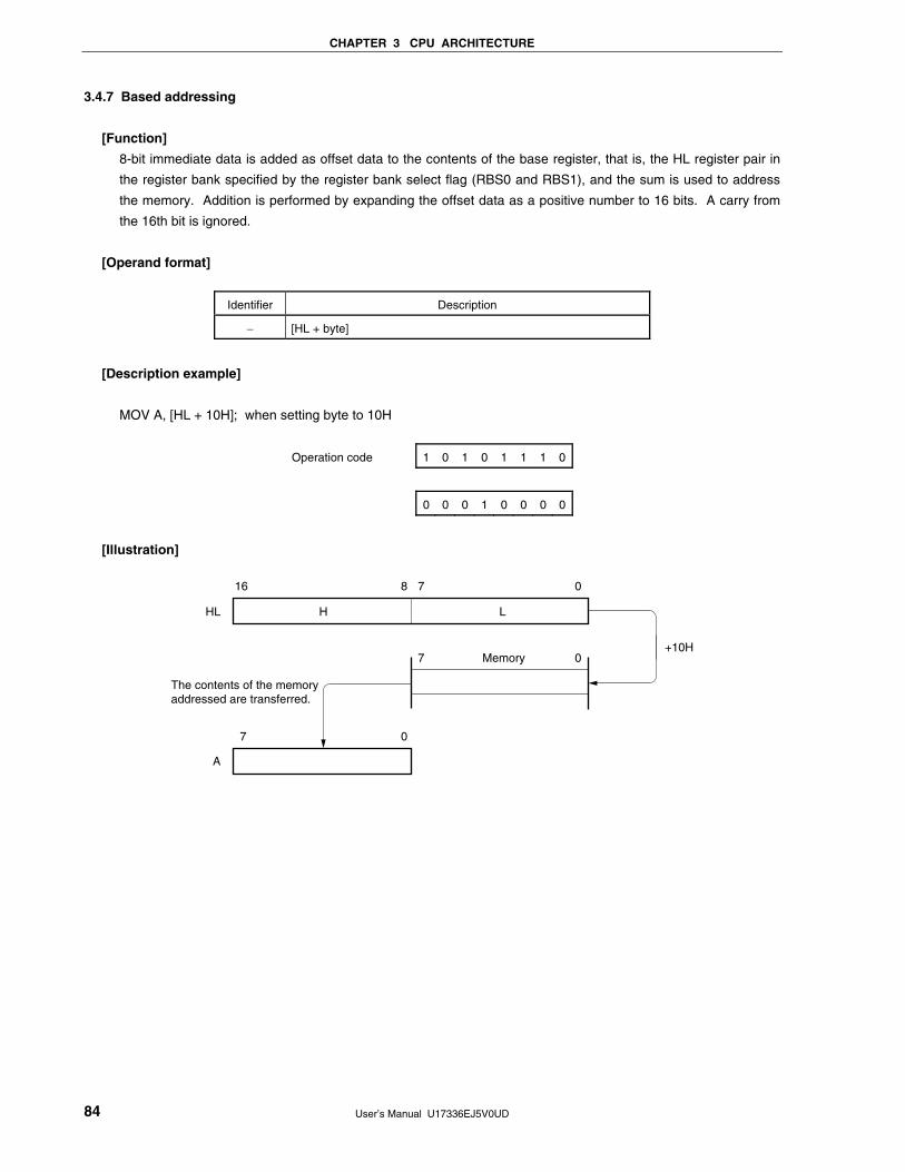
CHAPTER 3 CPU ARCHITECTURE
User’s Manual U17336EJ5V0UD 84
3.4.7 Based addressing
[Function]
8-bit immediate data is added as offset data to the contents of the base register, that is, the HL register pair in
the register bank specified by the register bank select flag (RBS0 and RBS1), and the sum is used to address
the memory. Addition is performed by expanding the offset data as a positive number to 16 bits. A carry from
the 16th bit is ignored.
[Operand format]
Identifier Description
− [HL + byte]
[Description example]
MOV A, [HL + 10H]; when setting byte to 10H
Operation code 1 0 1 0 1 1 1 0
0 0 0 1 0 0 0 0
[Illustration]
16 08
H
7
L
07
7 0
A
HL
The contents of the memoryaddressed are transferred.
Memory+10H

CHAPTER 3 CPU ARCHITECTURE
User’s Manual U17336EJ5V0UD 85
3.4.8 Based indexed addressing
[Function]
The B or C register contents specified in an instruction word are added to the contents of the base register, that
is, the HL register pair in the register bank specified by the register bank select flag (RBS0 and RBS1), and the
sum is used to address the memory. Addition is performed by expanding the B or C register contents as a
positive number to 16 bits. A carry from the 16th bit is ignored.
[Operand format]
Identifier Description
− [HL + B], [HL + C]
[Description example]
MOV A, [HL +B]; when selecting B register
Operation code 1 0 1 0 1 0 1 1
[Illustration]
16 0
H
78
L
07
B
+
07
7 0
A
HL
The contents of the memoryaddressed are transferred.
Memory


User’s Manual U17336EJ5V0UD 87
CHAPTER 4 PORT FUNCTIONS
4.1 Port Functions
There are two types of pin I/O buffer power supplies: AVREF and VDD. The relationship between these power
supplies and the pins is shown below.
Table 4-1. Pin I/O Buffer Power Supplies
Power Supply Corresponding Pins
AVREF P20 to P27
VDD Pins other than P20 to P27
78K0/KC2 products are provided with the ports shown in Figure 4-1, which enable variety of control operations.
The functions of each port are shown in Table 4-2.
In addition to the function as digital I/O ports, these ports have several alternate functions. For details of the
alternate functions, see CHAPTER 2 PIN FUNCTIONS.
Figure 4-1. Port Types
Port 0P00P01
P60
P63
P70
P75Note 2
P120
P140Note 2
P130Note 2
P124
Port 6
Port 7
Port 12
Port 14
Port 13
Port 2
P20
P27Note 1
Port 3
P30
P33
Port 1
P10
P17
Port 4P40Note 1
P41Note 1
P74Note 2P73Note 1P72Note 1P71
P26Note 1
Notes 1. 44-pin and 48-pin products only
2. 48-pin products only
<R>

CHAPTER 4 PORT FUNCTIONS
User’s Manual U17336EJ5V0UD 88
Table 4-2. Port Functions (1/2)
Function Name I/O Function After Reset Alternate Function
P00 TI000
P01
I/O Port 0.
2-bit I/O port.
Input/output can be specified in 1-bit units.
Use of an on-chip pull-up resistor can be specified by a software
setting.
Input port
TI010/TO00
P10 SCK10/TxD0
P11 SI10/RxD0
P12 SO10
P13 TxD6
P14 RxD6
P15 TOH0
P16 TOH1/INTP5
P17
I/O Port 1.
8-bit I/O port.
Input/output can be specified in 1-bit units.
Use of an on-chip pull-up resistor can be specified by a software
setting.
Input port
TI50/TO50
P20 to P25 ANI0 to ANI5
P26Note 1 and P27Note 1
I/O Port 2.
8-bit I/O port.
Input/output can be specified in 1-bit units.
Analog
input ANI6Note 1 and ANI7Note 1
P30 INTP1
P31 INTP2/OCD1ANote 2
P32 INTP3/OCD1BNote 2
P33
I/O Port 3.
4-bit I/O port.
Input/output can be specified in 1-bit units.
Use of an on-chip pull-up resistor can be specified by a software
setting.
Input port
TI51/TO51/INTP4
P40Note 1 and P41Note 1 I/O Port 4.
2-bit I/O port.
Input/output can be specified in 1-bit units.
Use of an on-chip pull-up resistor can be specified by a software
setting.
Input port −
P60 SCL0
P61 SDA0
P62 EXSCL0
P63
I/O Port 6.
4-bit I/O port.
Output of P60 to P63 is N-ch open-drain output (6 V tolerance).
Input/output can be specified in 1-bit units.
Input port
−
P70 and P71 KR0 and KR1
P72Note 1 and P73Note 1 KR2Note 1 and KR3Note 1
P74Note 3 and P75Note 3
I/O Port 7.
6-bit I/O port.
Input/output can be specified in 1-bit units.
Use of an on-chip pull-up resistor can be specified by a software
setting.
Input port
−
P120 INTP0/EXLVI
P121 X1/OCD0ANote 2
P122 X2/EXCLK/OCD0BNote 2
P123 XT1
P124
I/O Port 12.
5-bit I/O port.
Input/output can be specified in 1-bit units.
Only for P120, use of an on-chip pull-up resistor can be
specified by a software setting.
Input port
XT2/EXCLKS
P130Note 3 Output Port 13.
1-bit output-only port.
Output port −
Notes 1. 44-pin and 48-pin products only
For the 38-pin products, be sure to set bits 6 and 7 of PM2 to “1”, and bits 0 and 1 of PM4, bits 2 and 3 of
PM7, bits 6 and 7 of P2, bits 0 and 1 of P4, and bits 2 and 3 of P7 to “0”.
2. μPD78F0513D and 78F0515D only
3. 48-pin products only
<R>

CHAPTER 4 PORT FUNCTIONS
User’s Manual U17336EJ5V0UD 89
Table 4-2. Port Functions (2/2)
Function Name I/O Function After Reset Alternate Function
P140 Note I/O Port 14.
1-bit I/O port.
Input/output can be specified in 1-bit units.
Use of an on-chip pull-up resistor can be specified by a
software setting.
Input port PCL/INTP6 Note
Note 48-pin products only
4.2 Port Configuration
Ports include the following hardware.
Table 4-3. Port Configuration
Item Configuration
Control registers Port mode register (PM0 to PM4, PM6, PM7, PM12, PM14Note)
Port register (P0 to P4, P6, P7, P12, P13Note, P14Note)
Pull-up resistor option register (PU0, PU1, PU3, PU4, PU7, PU12, PU14Note)
A/D port configuration register (ADPC)
Port • 38-pin products
Total: 31 (CMOS I/O: 27, CMOS output: 0, N-ch open drain I/O: 4)
• 44-pin products
Total: 37 (CMOS I/O: 33, CMOS output: 0, N-ch open drain I/O: 4)
• 48-pin products
Total: 41 (CMOS I/O: 36, CMOS output: 1, N-ch open drain I/O: 4)
Pull-up resistor • 38-pin products Total: 17
• 44-pin products Total: 21
• 48-pin products Total: 24
Note 48-pin products only
<R>
<R>

CHAPTER 4 PORT FUNCTIONS
User’s Manual U17336EJ5V0UD 90
4.2.1 Port 0
Port 0 is a 2-bit I/O port with an output latch. Port 0 can be set to the input mode or output mode in 1-bit units
using port mode register 0 (PM0). When the P00 and P01 pins are used as an input port, use of an on-chip pull-up
resistor can be specified in 1-bit units by pull-up resistor option register 0 (PU0).
This port can also be used for timer I/O.
Reset signal generation sets port 0 to input mode.
Figures 4-2 and 4-3 show block diagrams of port 0.
Figure 4-2. Block Diagram of P00
Inte
rnal
bus
P00/TI000
WRPU
RD
PU0
PM0
WRPORT
WRPM
PU00
Alternate function
Output latch(P00)
PM00
VDD
P-ch
P0
Sel
ecto
r
P0: Port register 0
PU0: Pull-up resistor option register 0
PM0: Port mode register 0
RD: Read signal
WR××: Write signal

CHAPTER 4 PORT FUNCTIONS
User’s Manual U17336EJ5V0UD 91
Figure 4-3. Block Diagram of P01
P01/TI010/TO00
WRPU
RD
WRPORT
WRPM
PU01
PM01
VDD
P-ch
PU0
PM0
P0Inte
rnal
bus
Alternate function
Output latch(P01)
Sel
ecto
r
Alternate function
P0: Port register 0
PU0: Pull-up resistor option register 0
PM0: Port mode register 0
RD: Read signal
WR××: Write signal

CHAPTER 4 PORT FUNCTIONS
User’s Manual U17336EJ5V0UD 92
4.2.2 Port 1
Port 1 is an 8-bit I/O port with an output latch. Port 1 can be set to the input mode or output mode in 1-bit units
using port mode register 1 (PM1). When the P10 to P17 pins are used as an input port, use of an on-chip pull-up
resistor can be specified in 1-bit units by pull-up resistor option register 1 (PU1).
This port can also be used for external interrupt request input, serial interface data I/O, clock I/O, and timer I/O.
Reset signal generation sets port 1 to input mode.
Figures 4-4 to 4-8 show block diagrams of port 1.
Caution To use P10/SCK10/TxD0 and P12/SO10 as general-purpose ports, set serial operation mode
register 10 (CSIM10) and serial clock selection register 10 (CSIC10) to the default status (00H).
Figure 4-4. Block Diagram of P10
P10/SCK10/TxD0
WRPU
RD
WRPORT
WRPM
PU10
Alternatefunction
Output latch(P10)
PM10
Alternatefunction
VDD
P-ch
Sel
ecto
r
Inte
rnal
bus
PU1
PM1
P1
P1: Port register 1
PU1: Pull-up resistor option register 1
PM1: Port mode register 1
RD: Read signal
WR××: Write signal

CHAPTER 4 PORT FUNCTIONS
User’s Manual U17336EJ5V0UD 93
Figure 4-5. Block Diagram of P11 and P14
P11/SI10/RxD0,P14/RxD6
WRPU
RD
WRPORT
WRPM
PU11, PU14
Alternatefunction
Output latch(P11, P14)
PM11, PM14
VDD
P-ch
Sel
ecto
r
Inte
rnal
bus
PU1
PM1
P1
P1: Port register 1
PU1: Pull-up resistor option register 1
PM1: Port mode register 1
RD: Read signal
WR××: Write signal

CHAPTER 4 PORT FUNCTIONS
User’s Manual U17336EJ5V0UD 94
Figure 4-6. Block Diagram of P12 and P15
P12/SO10P15/TOH0
WRPU
RD
WRPORT
WRPM
PU12, PU15
Output latch(P12, P15)
PM12, PM15
Alternatefunction
VDD
P-ch
Sel
ecto
r
Inte
rnal
bus
PU1
PM1
P1
P1: Port register 1
PU1: Pull-up resistor option register 1
PM1: Port mode register 1
RD: Read signal
WR××: Write signal

CHAPTER 4 PORT FUNCTIONS
User’s Manual U17336EJ5V0UD 95
Figure 4-7. Block Diagram of P13
P13/TxD6
WRPU
RD
WRPORT
WRPM
PU13
Output latch(P13)
PM13
Alternatefunction
VDD
P-ch
Inte
rnal
bus
Sel
ecto
r
PU1
PM1
P1
P1: Port register 1
PU1: Pull-up resistor option register 1
PM1: Port mode register 1
RD: Read signal
WR××: Write signal
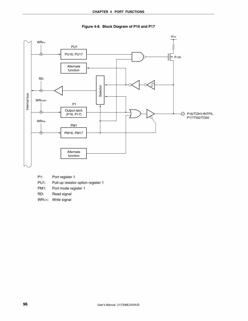
CHAPTER 4 PORT FUNCTIONS
User’s Manual U17336EJ5V0UD 96
Figure 4-8. Block Diagram of P16 and P17
P16/TOH1/INTP5,P17/TI50/TO50
WRPU
RD
WRPORT
WRPM
PU16, PU17
Alternatefunction
Output latch(P16, P17)
PM16, PM17
Alternatefunction
VDD
P-ch
Sel
ecto
r
Inte
rnal
bus
PU1
PM1
P1
P1: Port register 1
PU1: Pull-up resistor option register 1
PM1: Port mode register 1
RD: Read signal
WR××: Write signal

CHAPTER 4 PORT FUNCTIONS
User’s Manual U17336EJ5V0UD 97
4.2.3 Port 2
Port 2 is an 8-bit I/O port with an output latch. Port 2 can be set to the input mode or output mode in 1-bit units
using port mode register 2 (PM2).
This port can also be used for A/D converter analog input.
To use P20/ANI0 to P27/ANI7Note as digital input pins, set them in the digital I/O mode by using the A/D port
configuration register (ADPC) and in the input mode by using PM2. Use these pins starting from the lower bit.
To use P20/ANI0 to P27/ANI7Note as digital output pins, set them in the digital I/O mode by using ADPC and in the
output mode by using PM2.
Table 4-4. Setting Functions of P20/ANI0 to P27/ANI7Note Pins
ADPC PM2 ADS P20/ANI0 to P27/ANI7Note Pins
Input mode − Digital input Digital I/O selection
Output mode − Digital output
Selects ANI. Analog input (to be converted) Input mode
Does not select ANI. Analog input (not to be converted)
Selects ANI.
Analog input selection
Output mode
Does not select ANI.
Setting prohibited
All P20/ANI0 to P27/ANI7Note are set in the analog input mode when the reset signal is generated.
Figure 4-9 shows a block diagram of port 2.
Note 38-pin products: P20/ANI0 to P25/ANI5
44-pin and 48-pin products: P20/ANI0 to P27/ANI7
Cautions 1. Make the AVREF pin the same potential as the VDD pin when port 2 is used as a digital port.
2. For the 38-pin products, be sure to set bits 6 and 7 of PM2 to “1”, and bits 6 and 7 of P2 to “0”.
<R>
<R>

CHAPTER 4 PORT FUNCTIONS
User’s Manual U17336EJ5V0UD 98
Figure 4-9. Block Diagram of P20 to P27
In
tern
al b
us
P20/ANI0 to P27/ANI7Note
RD
WRPORT
WRPM
Output latch(P20 to P27)
PM20 to PM27S
elec
tor
PM2
A/D converter
P2
Note 38-pin products: P20/ANI0 to P25/ANI5
44-pin and 48-pin products: P20/ANI0 to P27/ANI7
P2: Port register 2
PM2: Port mode register 2
RD: Read signal
WR××: Write signal
<R>

CHAPTER 4 PORT FUNCTIONS
User’s Manual U17336EJ5V0UD 99
4.2.4 Port 3
Port 3 is a 4-bit I/O port with an output latch. Port 3 can be set to the input mode or output mode in 1-bit units
using port mode register 3 (PM3). When the P30 to P33 pins are used as an input port, use of an on-chip pull-up
resistor can be specified in 1-bit units by pull-up resistor option register 3 (PU3).
This port can also be used for external interrupt request input and timer I/O.
Reset signal generation sets port 3 to input mode.
Figures 4-10 and 4-11 show block diagrams of port 3.
Cautions 1. In the products with an on-chip debug function (μPD78F0513D and 78F0515D), be sure to pull
the P31/INTP2/OCD1ANote pin down before a reset release, to prevent malfunction.
2. For products without an on-chip debug function, with the flash memory of 48 KB or more
(μPD78F0514 and 78F0515), and having a product rank of “I”, “K”, or “E”, and for the
products with an on-chip debug function (μPD78F0513D and 78F0515D), connect
P31/INTP2/OCD1ANote as follows when writing the flash memory with a flash memory
programmer.
• P31/INTP2/OCD1ANote: Connect to VSS via a resistor (10 kΩ: recommended).
The above connection is not necessary when writing the flash memory by means of self
programming.
Note OCD1A is provided to the μPD78F0513D and 78F0515D only.
Remarks 1. For the product ranks, consult an NEC Electronics sales representative.
2. Only for the μPD78F0513D and 78F0515D, P31 and P32 can be used as on-chip debug mode
setting pins (OCD1A, OCD1B) when the on-chip debug function is used. For how to connect an in-
circuit emulator supporting on-chip debugging (QB-78K0MINI or QB-MINI2), see CHAPTER 26
ON-CHIP DEBUG FUNCTION (μPD78F0513D AND 78F0515D ONLY).
<R>
<R>

CHAPTER 4 PORT FUNCTIONS
User’s Manual U17336EJ5V0UD 100
Figure 4-10. Block Diagram of P30 to P32
P30/INTP1, P31/INTP2/OCD1ANote,P32/INTP3/OCD1BNote
WRPU
RD
WRPORT
WRPM
PU30 to PU32
Alternatefunction
Output latch(P30 to P32)
PM30 to PM32
VDD
P-ch
Sel
ecto
r
Inte
rnal
bus
PU3
PM3
P3
Note μPD78F0513D and 78F0515D only
P3: Port register 3
PU3: Pull-up resistor option register 3
PM3: Port mode register 3
RD: Read signal
WR××: Write signal

CHAPTER 4 PORT FUNCTIONS
User’s Manual U17336EJ5V0UD 101
Figure 4-11. Block Diagram of P33
P33/INTP4/TI51/TO51
WRPU
RD
WRPORT
WRPM
PU33
Alternatefunction
Output latch(P33)
PM33
Alternatefunction
VDD
P-ch
Sel
ecto
r
Inte
rnal
bus
PU3
PM3
P3
P3: Port register 3
PU3: Pull-up resistor option register 3
PM3: Port mode register 3
RD: Read signal
WR××: Write signal

CHAPTER 4 PORT FUNCTIONS
User’s Manual U17336EJ5V0UD 102
4.2.5 Port 4 (44-pin and 48-pin products only)
Port 4 is a 2-bit I/O port with an output latch. Port 4 can be set to the input mode or output mode in 1-bit units
using port mode register 4 (PM4). When the P40 and P41 pins are used as an input port, use of an on-chip pull-up
resistor can be specified in 1-bit units by pull-up resistor option register 4 (PU4).
Reset signal generation sets port 4 to input mode.
Figure 4-12 shows a block diagram of port 4.
Caution For the 38-pin products, be sure to set bits 0 and 1 of PM4 and P4 to “0”.
Figure 4-12. Block Diagram of P40, P41 (44-Pin and 48-Pin Products Only)
RD
P40, P41
P-ch
WRPU
WRPORT
WRPM
PU40, PU41
PM40, PM41
VDD
PU4
PM4
P4Inte
rnal
bus
Output latch(P40, P41)
Selector
P4: Port register 4
PU4: Pull-up resistor option register 4
PM4: Port mode register 4
RD: Read signal
WR××: Write signal
<R>

CHAPTER 4 PORT FUNCTIONS
User’s Manual U17336EJ5V0UD 103
4.2.6 Port 6
Port 6 is a 4-bit I/O port with an output latch. Port 6 can be set to the input mode or output mode in 1-bit units
using port mode register 6 (PM6).
The output of the P60 to P63 pins is N-ch open-drain output (6 V tolerance).
This port can also be used for serial interface data I/O, clock I/O, and external clock input.
Reset signal generation sets port 6 to input mode.
Figures 4-13 to 4-15 show block diagrams of port 6.
Remark When using P62/EXSCL0 as an external clock input pin of the serial interface, input a clock of 6.4 MHz
to it.
Figure 4-13. Block Diagram of P60 and P61
P60/SCL0,P61/SDA0
RD
WRPORT
WRPM
Alternatefunction
Output latch(P60, P61)
PM60, PM61
Alternatefunction
Inte
rnal
bus
Sel
ecto
r
PM6
P6
P6: Port register 6
PM6: Port mode register 6
RD: Read signal
WR××: Write signal
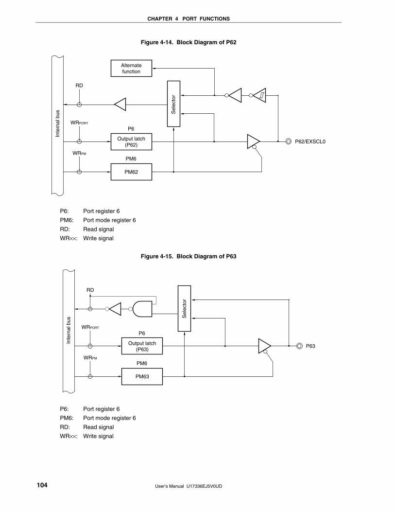
CHAPTER 4 PORT FUNCTIONS
User’s Manual U17336EJ5V0UD 104
Figure 4-14. Block Diagram of P62
P62/EXSCL0
RD
WRPORT
WRPM
Alternatefunction
Output latch(P62)
PM62
Inte
rnal
bus S
elec
tor
PM6
P6
P6: Port register 6
PM6: Port mode register 6
RD: Read signal
WR××: Write signal
Figure 4-15. Block Diagram of P63
P63
RD
WRPORT
WRPM
Output latch(P63)
PM63
Inte
rnal
bus
Sel
ecto
r
PM6
P6
P6: Port register 6
PM6: Port mode register 6
RD: Read signal
WR××: Write signal

CHAPTER 4 PORT FUNCTIONS
User’s Manual U17336EJ5V0UD 105
4.2.7 Port 7
Port 7 is a 6-bit I/O port with an output latch. Port 7 can be set to the input mode or output mode in 1-bit units
using port mode register 7 (PM7). When the P70 to P75Note pins are used as an input port, use of an on-chip pull-up
resistor can be specified in 1-bit units by pull-up resistor option register 7 (PU7).
P70 to P73 can also be used for key return input.
Reset signal generation sets port 7 to input mode.
Figure 4-16 shows a block diagram of port 7.
Note 38-pin products: P70/KR0, P71/KR1
44-pin products: P70/KR0 to P73/KR3
48-pin products: P70/KR0 to P73/KR3, P74, P75
Caution For the 38-pin products, be sure to set bits 2 and 3 of PM7 and P7 to “0”.
Figure 4-16. Block Diagram of P70 to P75
P70/KR0 to P73/KR3Note 1,P74Note 1, P75Note 1
WRPU
RD
WRPORT
WRPM
PU70 to PU75Note 2
Alternate functionNote 3
Output latch(P70 to P75Notes 2, 4)
PM70 to PM75Notes 2, 4
VDD
P-ch
Sel
ecto
r
Inte
rnal
bus
PU7
PM7
Notes 1. 38-pin products: P70/KR0, P71/KR1
44-pin products: P70/KR0 to P73/KR3
48-pin products: P70/KR0 to P73/KR3, P74, P75
2. P74, P75, PM74, PM75, PU74, and PU75 are available only in the 48-pin products.
3. The alternate function is available only in the P70 to P73 pins.
P7: Port register 7
PU7: Pull-up resistor option register 7
PM7: Port mode register 7
RD: Read signal
WR××: Write signal
<R>
<R>
<R>

CHAPTER 4 PORT FUNCTIONS
User’s Manual U17336EJ5V0UD 106
4.2.8 Port 12
Port 12 is a 5-bit I/O port with an output latch. Port 12 can be set to the input mode or output mode in 1-bit units
using port mode register 12 (PM12). When used as an input port only for P120, use of an on-chip pull-up resistor can
be specified by pull-up resistor option register 12 (PU12).
This port can also be used as pins for external interrupt request input, potential input for external low-voltage
detection, connecting resonator for main system clock, connecting resonator for subsystem clock, external clock input
for main system clock, and external clock input for subsystem clock.
Reset signal generation sets port 12 to input mode.
Figures 4-17 and 4-18 show block diagrams of port 12.
Cautions 1. When using the P121 to P124 pins to connect a resonator for the main system clock (X1, X2)
or subsystem clock (XT1, XT2), or to input an external clock for the main system clock
(EXCLK) or subsystem clock (EXCLKS), the X1 oscillation mode, XT1 oscillation mode, or
external clock input mode must be set by using the clock operation mode select register
(OSCCTL) (for details, see 5.3 (1) Clock operation mode select register (OSCCTL) and (3)
Setting of operation mode for subsystem clock pin). The reset value of OSCCTL is 00H (all of
the P121 to P124 pins are I/O port pins). At this time, setting of the PM121 to PM124 and
P121 to P124 pins is not necessary.
2. For products without an on-chip debug function, with the flash memory of 48 KB or more
(μPD78F0514 and 78F0515), and having a product rank of “I”, “K”, or “E”, and for the product
with an on-chip debug function (μPD78F0513D and 78F0515D), connect P121/X1/OCD0ANote as
follows when writing the flash memory with a flash memory programmer.
• P121/X1/OCD0ANote: When using this pin as a port, connect it to VSS via a resistor (10 kΩ:
recommended) (in the input mode) or leave it open (in the output
mode).
The above connection is not necessary when writing the flash memory by means of self
programming.
Note OCD0A is provided to the μPD78F0513D and 78F0515D only.
Remarks 1. For the product ranks, consult an NEC Electronics sales representative.
2. The X1 and X2 pins of the μPD78F0513D and 78F0515D can be used as on-chip debug mode
setting pins (OCD0A, OCD0B) when the on-chip debug function is used. For how to connect an in-
circuit emulator supporting on-chip debugging (QB-78K0MINI or QB-MINI2), see CHAPTER 26 ON-
CHIP DEBUG FUNCTION (μPD78F0513D AND 78F0515D ONLY).
<R>
<R>

CHAPTER 4 PORT FUNCTIONS
User’s Manual U17336EJ5V0UD 107
Figure 4-17. Block Diagram of P120
P120/INTP0/EXLVI
WRPU
RD
WRPORT
WRPM
PU120
Alternatefunction
Output latch(P120)
PM120
VDD
P-ch
PU12
PM12
P12
Sel
ecto
r
Inte
rnal
bus
P12: Port register 12
PU12: Pull-up resistor option register 12
PM12: Port mode register 12
RD: Read signal
WR××: Write signal
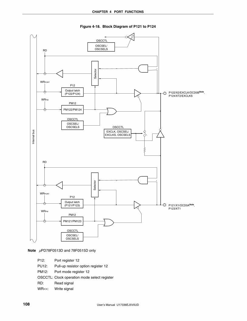
CHAPTER 4 PORT FUNCTIONS
User’s Manual U17336EJ5V0UD 108
Figure 4-18. Block Diagram of P121 to P124
P122/X2/EXCLK/OCD0BNote, P124/XT2/EXCLKS
RD
WRPORT
WRPM
Output latch(P122/P124)
PM122/PM124
PM12
P12
RD
WRPORT
WRPM
Output latch(P121/P123)
PM121/PM123
PM12
P12
EXCLK, OSCSEL/EXCLKS, OSCSELS
OSCCTL
OSCSEL/OSCSELS
OSCCTL
P121/X1/OCD0ANote, P123/XT1
OSCSEL/OSCSELS
OSCCTL
OSCSEL/OSCSELS
OSCCTL
Inte
rnal
bus
Sel
ecto
rS
elec
tor
Note μPD78F0513D and 78F0515D only
P12: Port register 12
PU12: Pull-up resistor option register 12
PM12: Port mode register 12
OSCCTL: Clock operation mode select register
RD: Read signal
WR××: Write signal

CHAPTER 4 PORT FUNCTIONS
User’s Manual U17336EJ5V0UD 109
4.2.9 Port 13 (48-pin products only)
Port 13 is a 1-bit output-only port.
Figure 4-19 shows a block diagram of port 13.
Figure 4-19. Block Diagram of P130 (48-Pin Products Only)
RD
Output latch(P130)
WRPORT
P130
Inte
rnal
bus
P13
P13: Port register 13
RD: Read signal
WR××: Write signal
Remark When reset is effected, P130 outputs a low level. If P130 is set to output a high level before reset is
effected, the output signal of P130 can be dummy-output as the CPU reset signal.
P130
Set by software
Reset signal

CHAPTER 4 PORT FUNCTIONS
User’s Manual U17336EJ5V0UD 110
4.2.10 Port 14 (48-pin products only)
Port 14 is a 1-bit I/O port with an output latch. Port 14 can be set to the input mode or output mode in 1-bit units
using port mode register 14 (PM14). When the P140 pin is used as an input port, use of an on-chip pull-up resistor
can be specified in 1-bit units by pull-up resistor option register 14 (PU14).
This port can also be used for external interrupt request input and clock output.
Reset signal generation sets port 14 to input mode.
Figures 4-20 shows a block diagram of port 14.
Figure 4-20. Block Diagram of P140 (48-Pin Products Only)
P140/PCL/INTP6
WRPU
RD
WRPORT
WRPM
PU140
Alternatefunction
Output latch(P140)
PM140
Alternatefunction
VDD
P-chS
elec
tor
Inte
rnal
bus
PU14
PM14
P14
P14: Port register 14
PU14: Pull-up resistor option register 14
PM14: Port mode register 14
RD: Read signal
WR××: Write signal

CHAPTER 4 PORT FUNCTIONS
User’s Manual U17336EJ5V0UD 111
4.3 Registers Controlling Port Function
Port functions are controlled by the following four types of registers.
• Port mode registers (PM0 to PM4, PM6, PM7, PM12, PM14Note)
• Port registers (P0 to P4, P6, P7, P12, P13Note, P14Note)
• Pull-up resistor option registers (PU0, PU1, PU3, PU4, PU7, PU12, PU14Note)
• A/D port configuration register (ADPC)
Note 48-pin products only
(1) Port mode registers (PM0 to PM4, PM6, PM7, PM12, and PM14Note)
These registers specify input or output mode for the port in 1-bit units.
These registers can be set by a 1-bit or 8-bit memory manipulation instruction.
Reset signal generation sets these registers to FFH.
When port pins are used as alternate-function pins, set the port mode register by referencing 4.5 Settings of
Port Mode Register and Output Latch When Using Alternate Function.
Note 48-pin products only

CHAPTER 4 PORT FUNCTIONS
User’s Manual U17336EJ5V0UD 112
Figure 4-21. Format of Port Mode Register
7
1
Symbol
PM0
6
1
5
1
4
1
3
1
2
1
1
PM01
0
PM00
Address
FF20H
After reset
FFH
R/W
R/W
PM17PM1 PM16 PM15 PM14 PM13 PM12 PM11 PM10 FF21H FFH R/W
PM27PM2 PM26 PM25 PM24 PM23 PM22 PM21 PM20 FF22H FFH R/W
1PM3 1 1 1 PM33 PM32 PM31 PM30 FF23H FFH R/W
1PM4 1 1 1 1 1 PM41 PM40 FF24H FFH R/W
1PM6 1 1 1 PM63 PM62 PM61 PM60 FF26H FFH R/W
1PM7 1 PM75Note PM74Note PM73 PM72 PM71 PM70 FF27H FFH R/W
1PM12 1 1 PM124 PM123 PM122 PM121 PM120 FF2CH FFH R/W
1PM14Note 1 1 1 1 1 1 PM140 FF2EH FFH R/W
PMmn Pmn pin I/O mode selection
(m = 0 to 4, 6, 7, 12, 14; n = 0 to 7)
0 Output mode (output buffer on)
1 Input mode (output buffer off)
Note 48-pin products only
Caution For the 38-pin products, be sure to set bits 2 to 7 of PM0, bits 6 and 7 of PM2, bits 4 to 7
of PM3, bits 2 to 7 of PM4, bits 4 to 7 of PM6, bits 4 to 7 of PM7, and bits 5 to 7 of PM12
to “1”. Also, be sure to set bits 0 and 1 of PM4, and bits 2 and 3 of PM7 to “0”.
For the 44-pin products, be sure to set bits 2 to 7 of PM0, bits 4 to 7 of PM3, bits 2 to 7 of
PM4, bits 4 to 7 of PM6, bits 4 to 7 of PM7, and bits 5 to 7 of PM12 to “1”.
For the 48-pin products, be sure to set bits 2 to 7 of PM0, bits 4 to 7 of PM3, bits 2 to 7 of
PM4, bits 4 to 7 of PM6, bits 6 and 7 of PM7, bits 5 to 7 of PM12, and bits 1 to 7 of PM14
to “1”.
<R>

CHAPTER 4 PORT FUNCTIONS
User’s Manual U17336EJ5V0UD 113
(2) Port registers (P0 to P4, P6, P7, P12, P13Note, and P14Note)
These registers write the data that is output from the chip when data is output from a port.
If the data is read in the input mode, the pin level is read. If it is read in the output mode, the value of the output
latch is read.
These registers can be set by a 1-bit or 8-bit memory manipulation instruction.
Reset signal generation sets these registers to 00H.
Note 48-pin products only
Figure 4-22. Format of Port Register
7
0
Symbol
P0
6
0
5
0
4
0
3
0
2
0
1
P01
0
P00
Address
FF00H
After reset
00H (output latch)
R/W
R/W
P17P1 P16 P15 P14 P13 P12 P11 P10 FF01H 00H (output latch) R/W
R/WP27P2 P26 P25 P24 P23 P22 P21 P20 FF02H 00H (output latch)
0P3 0 0 0 P33 P32 P31 P30 FF03H 00H (output latch) R/W
0P4 0 0 0 0 0 P41 P40 FF04H 00H (output latch) R/W
0P6 0 0 0 P63 P62 P61 P60 FF06H 00H (output latch) R/W
0P7 0 P75Note 1 P74Note 1 P73 P72 P71 P70 FF07H 00H (output latch) R/W
0P12 0 0 P124Note 2 P123Note 2 P122Note 2 P121Note 2 P120 FF0CH 00H (output latch) R/W
0P13Note 1 0 0 0 0 0 0 P130Note 1 FF0DH 00H (output latch) R/W
0P14Note 1 0 0 0 0 0 0 P140Note 1 FF0EH 00H (output latch) R/W
m = 0 to 4, 6, 7, 12 to 14; n = 0 to 7
Pmn
Output data control (in output mode) Input data read (in input mode)
0 Output 0 Input low level
1 Output 1 Input high level
Notes 1. 48-pin products only
2. “0” is always read from the output latch of P121 to P124 if the pin is in the external clock input
mode.
Caution For the 38-pin products, be sure to set bits 6 and 7 of P2, bits 0 and 1 of P4, and bits 2 and
3 of P7 to “0”.
<R>

CHAPTER 4 PORT FUNCTIONS
User’s Manual U17336EJ5V0UD 114
(3) Pull-up resistor option registers (PU0, PU1, PU3, PU4, PU7, PU12, and PU14Note)
These registers specify whether the on-chip pull-up resistors of P00, P01, P10 to P17, P30 to P33, P40, P41, P70
to P73, P74Note, P75Note, P120, and P140Note are to be used or not. On-chip pull-up resistors can be used in 1-bit
units only for the bits set to input mode of the pins to which the use of an on-chip pull-up resistor has been
specified in PU0, PU1, PU3, PU4, PU7, PU12, and PU14Note. On-chip pull-up resistors cannot be connected to
bits set to output mode and bits used as alternate-function output pins, regardless of the settings of PU0, PU1,
PU3, PU4, PU7, PU12, and PU14Note.
These registers can be set by a 1-bit or 8-bit memory manipulation instruction.
Reset signal generation sets these registers to 00H.
Note 48-pin products only
Figure 4-23. Format of Pull-up Resistor Option Register
7
0
Symbol
PU0
6
0
5
0
4
0
3
0
2
0
1
PU01
0
PU00
Address
FF30H
After reset
00H
R/W
R/W
PU17PU1 PU16 PU15 PU14 PU13 PU12 PU11 PU10 FF31H 00H R/W
0PU3 0 0 0 PU33 PU32 PU31 PU30 FF33H 00H R/W
0PU4 0 0 0 0 0 PU41 PU40 FF34H 00H R/W
0PU7 0 PU75Note PU74Note PU73 PU72 PU71 PU70 FF37H 00H R/W
0PU12 0 0 0 0 0 0 PU120 FF3CH 00H R/W
0PU14Note 0 0 0 0 0 0 PU140 FF3EH 00H R/W
PUmn Pmn pin on-chip pull-up resistor selection
(m = 0, 1, 3, 4, 7, 12, 14; n = 0 to 7)
0 On-chip pull-up resistor not connected
1 On-chip pull-up resistor connected
Note 48-pin products only

CHAPTER 4 PORT FUNCTIONS
User’s Manual U17336EJ5V0UD 115
(4) A/D port configuration register (ADPC)
This register switches the P20/ANI0 to P27/ANI7Note pins to digital I/O of port or analog input of A/D converter.
ADPC can be set by a 1-bit or 8-bit memory manipulation instruction.
Reset signal generation sets this register to 00H.
Note 38-pin products: P20/ANI0 to P25/ANI5 pins
44-pin and 48-pin products: P20/ANI0 to P27/ANI7 pins
Figure 4-24. Format of A/D Port Configuration Register (ADPC)
ADPC0ADPC1ADPC2ADPC30000
Digital I/O (D)/analog input (A) switching
Setting prohibited
ADPC3
01234567
ADPC
Address: FF2FH After reset: 00H R/W
Symbol
P27/ANI7
A
A
A
A
A
A
A
A
D
P26/ANI6
A
A
A
A
A
A
A
D
D
P25/ANI5
A
A
A
A
A
A
D
D
D
P24/ANI4
A
A
A
A
A
D
D
D
D
P23/ANI3
A
A
A
A
D
D
D
D
D
P22/ANI2
A
A
A
D
D
D
D
D
D
P21/ANI1
A
A
D
D
D
D
D
D
D
P20/ANI0
A
D
D
D
D
D
D
D
D
0
0
0
0
0
0
0
0
1
ADPC2
0
0
0
0
1
1
1
1
0
ADPC1
0
0
1
1
0
0
1
1
0
ADPC0
0
1
0
1
0
1
0
1
0
Other than above
Cautions 1. Set the channel used for A/D conversion to the input mode by using port mode register 2
(PM2).
2. If data is written to ADPC, a wait cycle is generated. Do not write data to ADPC when the CPU
is operating on the subsystem clock and the peripheral hardware clock is stopped. For
details, see CHAPTER 34 CAUTIONS FOR WAIT.
3. For the 38-pin products, setting ADPC3, ADPC2, ADPC1, ADPC0 to 0, 1, 1, 1 or 1, 0, 0, 0 is
prohibited.
<R>
<R>
CHAPTER 4 PORT FUNCTIONS
User’s Manual U17336EJ5V0UD 116
4.4 Port Function Operations
Port operations differ depending on whether the input or output mode is set, as shown below.
4.4.1 Writing to I/O port
(1) Output mode
A value is written to the output latch by a transfer instruction, and the output latch contents are output from the pin.
Once data is written to the output latch, it is retained until data is written to the output latch again.
The data of the output latch is cleared when a reset signal is generated.
(2) Input mode
A value is written to the output latch by a transfer instruction, but since the output buffer is off, the pin status does
not change.
Once data is written to the output latch, it is retained until data is written to the output latch again.
The data of the output latch is cleared when a reset signal is generated.
4.4.2 Reading from I/O port
(1) Output mode
The output latch contents are read by a transfer instruction. The output latch contents do not change.
(2) Input mode
The pin status is read by a transfer instruction. The output latch contents do not change.
4.4.3 Operations on I/O port
(1) Output mode
An operation is performed on the output latch contents, and the result is written to the output latch. The output
latch contents are output from the pins.
Once data is written to the output latch, it is retained until data is written to the output latch again.
The data of the output latch is cleared when a reset signal is generated.
(2) Input mode
The pin level is read and an operation is performed on its contents. The result of the operation is written to the
output latch, but since the output buffer is off, the pin status does not change.
The data of the output latch is cleared when a reset signal is generated.

CHAPTER 4 PORT FUNCTIONS
User’s Manual U17336EJ5V0UD 117
4.5 Settings of Port Mode Register and Output Latch When Using Alternate Function
To use the alternate function of a port pin, set the port mode register and output latch as shown in Table 4-5.
Table 4-5. Settings of Port Mode Register and Output Latch When Using Alternate Function
Alternate Function Pin Name
Function Name I/O
PM×× P××
P00 TI000 Input 1 ×
TI010 Input 1 × P01
TO00 Output 0 0
Input 1 × SCK10
Output 0 1
P10
TxD0 Output 0 1
SI10 Input 1 × P11
RxD0 Input 1 ×
P12 SO10 Output 0 0
P13 TxD6 Output 0 1
P14 RxD6 Input 1 ×
P15 TOH0 Output 0 0
TOH1 Output 0 0 P16
INTP5 Input 1 ×
TI50 Input 1 × P17
TO50 Output 0 0
P20 to P27Notes 1, 2 ANI0 to ANI7Notes 1, 2 Input 1 ×
P30 to P32 INTP1 to INTP3 Input 1 ×
INTP4 Input 1 ×
TI51 Input 1 ×
P33
TO51 Output 0 0
P60 SCL0 I/O 0 0
P61 SDA0 I/O 0 0
P62 EXSCL0 Input 1 ×
P70 to P73Note 1 KR0 to KR3Note 1 Input 1 ×
INTP0 Input 1 × P120
EXLVI Input 1 ×
P121 X1Note 3 − × ×
X2Note 3 − × × P122
EXCLKNote 3 Input × ×
P123 XT1Note 3 − × ×
XT2Note 3 − × × P124
EXCLKSNote 3 Input × ×
PCL Output 0 0 P140Note 4
INTP6 Input 1 ×

CHAPTER 4 PORT FUNCTIONS
User’s Manual U17336EJ5V0UD 118
Notes 1. 38-pin products: P20/ANI0 to P25/ANI5, P70/KR0, P71/KR1
44-pin and 48-pin products: P20/ANI0 to P27/ANI7, P70/KR0 to P73/KR3
2. The function of the ANI0/P20 to ANI7/P27 pins can be selected by using the A/D port configuration
register (ADPC), the analog input channel specification register (ADS), and PM2.
Table 4-6. Setting Functions of ANI0/P20 to ANI7/P27 Pins
ADPC PM2 ADS ANI0/P20 to ANI7/P27 Pins
Selects ANI. Analog input (to be converted) Input mode
Does not select ANI. Analog input (not to be converted)
Selects ANI.
Analog input selection
Output mode
Does not select ANI.
Setting prohibited
Input mode − Digital input Digital I/O selection
Output mode − Digital output
3. When using the P121 to P124 pins to connect a resonator for the main system clock (X1, X2) or
subsystem clock (XT1, XT2), or to input an external clock for the main system clock (EXCLK) or
subsystem clock (EXCLKS), the X1 oscillation mode, XT1 oscillation mode, or external clock input
mode must be set by using the clock operation mode select register (OSCCTL) (for details, see 5.3 (1)
Clock operation mode select register (OSCCTL) and (3) Setting of operation mode for
subsystem clock pin). The reset value of OSCCTL is 00H (all of the P121 to P124 are I/O port pins).
At this time, setting of PM121 to PM124 and P121 to P124 is not necessary.
4. 48-pin products only
Remarks 1. ×: Don’t care
PM××: Port mode register
P××: Port output latch
2. The X1, X2, P31, and P32 pins of the μPD78F0513D and 78F0515D can be used as on-chip debug
mode setting pins (OCD0A, OCD0B, OCD1A, OCD1B) when the on-chip debug function is used. For
how to connect an in-circuit emulator supporting on-chip debugging (QB-78K0MINI or QB-MINI2),
see CHAPTER 26 ON-CHIP DEBUG FUNCTION (μPD78F0513D and 78F0515D ONLY).
<R>

CHAPTER 4 PORT FUNCTIONS
User’s Manual U17336EJ5V0UD 119
4.6 Cautions on 1-bit Manipulation Instruction for Port Register n (Pn)
When a 1-bit manipulation instruction is executed on a port that provides both input and output functions, the
output latch value of an input port that is not subject to manipulation may be written in addition to the targeted bit.
Therefore, it is recommended to rewrite the output latch when switching a port from input mode to output mode.
<Example> When P10 is an output port, P11 to P17 are input ports (all pin statuses are high level), and the port
latch value of port 1 is 00H, if the output of output port P10 is changed from low level to high level
via a 1-bit manipulation instruction, the output latch value of port 1 is FFH.
Explanation: The targets of writing to and reading from the Pn register of a port whose PMnm bit is 1 are the
output latch and pin status, respectively.
A 1-bit manipulation instruction is executed in the following order in the 78K0/KC2.
<1> The Pn register is read in 8-bit units.
<2> The targeted one bit is manipulated.
<3> The Pn register is written in 8-bit units.
In step <1>, the output latch value (0) of P10, which is an output port, is read, while the pin statuses
of P11 to P17, which are input ports, are read. If the pin statuses of P11 to P17 are high level at
this time, the read value is FEH.
The value is changed to FFH by the manipulation in <2>.
FFH is written to the output latch by the manipulation in <3>.
Figure 4-25. Bit Manipulation Instruction (P10)
Low-level output
1-bit manipulationinstruction (set1 P1.0)is executed for P10bit.
Pin status: High level
P10
P11 to P17
Port 1 output latch
0 0 0 0 0 0 0 0
High-level output
Pin status: High level
P10
P11 to P17
Port 1 output latch
1 1 1 1 1 1 1 1
1-bit manipulation instruction for P10 bit
<1> Port register 1 (P1) is read in 8-bit units.• In the case of P10, an output port, the value of the port output latch (0) is read.• In the case of P11 to P17, input ports, the pin status (1) is read.
<2> Set the P10 bit to 1.<3> Write the results of <2> to the output latch of port register 1 (P1)
in 8-bit units.

User’s Manual U17336EJ5V0UD 120
CHAPTER 5 CLOCK GENERATOR
5.1 Functions of Clock Generator
The clock generator generates the clock to be supplied to the CPU and peripheral hardware.
The following three kinds of system clocks and clock oscillators are selectable.
(1) Main system clock
<1> X1 oscillator
This circuit oscillates a clock of fX = 1 to 20 MHz by connecting a resonator to X1 and X2.
Oscillation can be stopped by executing the STOP instruction or using the main OSC control register
(MOC).
<2> Internal high-speed oscillator
This circuit oscillates a clock of fRH = 8 MHz (TYP.). After a reset release, the CPU always starts
operating with this internal high-speed oscillation clock. Oscillation can be stopped by executing the
STOP instruction or using the internal oscillation mode register (RCM).
An external main system clock (fEXCLK = 1 to 20 MHz) can also be supplied from the EXCLK/X2/P122 pin. An
external main system clock input can be disabled by executing the STOP instruction or using RCM.
As the main system clock, a high-speed system clock (X1 clock or external main system clock) or internal high-
speed oscillation clock can be selected by using the main clock mode register (MCM).
(2) Subsystem clock
• Subsystem clock oscillator
This circuit oscillates at a frequency of fXT = 32.768 kHz by connecting a 32.768 kHz resonator across XT1
and XT2. Oscillation can be stopped by using the processor clock control register (PCC) and clock
operation mode select register (OSCCTL).
An external subsystem clock (fEXCLKS = 32.768 kHz) can also be supplied from the EXCLKS/XT2/P124 pin. An
external subsystem clock input can be disabled by setting PCC and OSCCTL.
Remarks 1. fX: X1 clock oscillation frequency
2. fRH: Internal high-speed oscillation clock frequency
3. fEXCLK: External main system clock frequency
4. fXT: XT1 clock oscillation frequency
5. fEXCLKS: External subsystem clock frequency

CHAPTER 5 CLOCK GENERATOR
User’s Manual U17336EJ5V0UD 121
(3) Internal low-speed oscillation clock (clock for watchdog timer)
• Internal low-speed oscillator
This circuit oscillates a clock of fRL = 240 kHz (TYP.). After a reset release, the internal low-speed oscillation
clock always starts operating.
Oscillation can be stopped by using the internal oscillation mode register (RCM) when “internal low-speed
oscillator can be stopped by software” is set by option byte.
The internal low-speed oscillation clock cannot be used as the CPU clock. The following hardware operates
with the internal low-speed oscillation clock.
• Watchdog timer
• TMH1 (when fRL, fRL/27, or fRL/29 is selected)
Remark fRL: Internal low-speed oscillation clock frequency
5.2 Configuration of Clock Generator
The clock generator includes the following hardware.
Table 5-1. Configuration of Clock Generator
Item Configuration
Control registers Clock operation mode select register (OSCCTL) Processor clock control register (PCC) Internal oscillation mode register (RCM) Main OSC control register (MOC) Main clock mode register (MCM) Oscillation stabilization time counter status register (OSTC) Oscillation stabilization time select register (OSTS)
Oscillators X1 oscillator XT1 oscillator Internal high-speed oscillator Internal low-speed oscillator

CH
AP
TE
R 5 C
LO
CK
GE
NE
RA
TO
R
User’s M
anual U17336E
J5V0U
D
122
Figure 5-1. Block Diagram of Clock Generator
Option byte1: Cannot be stopped0: Can be stopped
Internal oscillationmode register
(RCM)
LSRSTOPRSTS RSTOP
Internal high-speed oscillator(8 MHz (TYP.))
Internal low-speed oscillator(240 kHz (TYP.))
fRL
Clock operation modeselect register(OSCCTL)
OSCSELSEXCLKS
XT1/P123
XT2/EXCLKS/P124
fSUB
Peripheral hardware clock (fPRS)
Watchdog timer, 8-bit timer H1
Watch timer, clock output
1/2
CPU clock(fCPU)
Processor clock control register (PCC)
CSS PCC2CLS PCC1 PCC0
PrescalerMain systemclock switch
fXP
Peripheralhardware
clock switch
X1 oscillationstabilization time counter
OSTS1 OSTS0OSTS2
Oscillation stabilization time select register (OSTS)
3
MOST16
MOST15
MOST14
MOST13
MOST11
Oscillation stabilization time counter status register (OSTC)
Controller
MCM0XSELMCSMSTOPEXCLK OSCSELAMPH
Clock operation modeselect register
(OSCCTL)
4
fXP
2fXP
22fXP
23fXP
24
Main clock mode register (MCM)
Main clockmode register(MCM)
Main OSCcontrol register
(MOC)
fRH
Internal bus
Internal bus
High-speed systemclock oscillator
Crystal/ceramicoscillation
External inputclock
X1/P121
X2/EXCLK/P122
fXH
fSUB
2
Crystaloscillation
External inputclock
Subsystemclock oscillator
fX
fEXCLK
fXT
fEXCLKS
XTSTART
To subsystemclock oscillator
XTSTART
Processor clockcontrol register
(PCC)
Sel
ecto
r
STOP

CHAPTER 5 CLOCK GENERATOR
User’s Manual U17336EJ5V0UD 123
Remarks 1. fX: X1 clock oscillation frequency
2. fRH: Internal high-speed oscillation clock frequency
3. fEXCLK: External main system clock frequency
4. fXH: High-speed system clock frequency
5. fXP: Main system clock frequency
6. fPRS: Peripheral hardware clock frequency
7. fCPU: CPU clock frequency
8. fXT: XT1 clock oscillation frequency
9. fEXCLKS: External subsystem clock frequency
10. fSUB: Subsystem clock frequency
11. fRL: Internal low-speed oscillation clock frequency
5.3 Registers Controlling Clock Generator
The following seven registers are used to control the clock generator.
• Clock operation mode select register (OSCCTL)
• Processor clock control register (PCC)
• Internal oscillation mode register (RCM)
• Main OSC control register (MOC)
• Main clock mode register (MCM)
• Oscillation stabilization time counter status register (OSTC)
• Oscillation stabilization time select register (OSTS)
(1) Clock operation mode select register (OSCCTL)
This register selects the operation modes of the high-speed system and subsystem clocks, and the gain of the
on-chip oscillator.
OSCCTL can be set by a 1-bit or 8-bit memory manipulation instruction.
Reset signal generation clears this register to 00H.

CHAPTER 5 CLOCK GENERATOR
User’s Manual U17336EJ5V0UD 124
Figure 5-2. Format of Clock Operation Mode Select Register (OSCCTL)
Address: FF9FH After reset: 00H R/W
Symbol <7> <6> <5> <4> 3 2 1 <0>
OSCCTL EXCLK OSCSEL EXCLKSNote OSCSELSNote 0 0 0 AMPH
EXCLK OSCSEL High-speed system clock pin operation mode
P121/X1 pin P122/X2/EXCLK pin
0 0 I/O port mode I/O port
0 1 X1 oscillation mode Crystal/ceramic resonator connection
1 0 I/O port mode I/O port
1 1 External clock input
mode
I/O port External clock input
AMPH Operating frequency control
0 1 MHz ≤ fXH ≤ 10 MHz
1 10 MHz < fXH ≤ 20 MHz
Note EXCLKS and OSCSELS are used in combination with XTSTART (bit 6 of the processor
clock control register (PCC)). See (3) Setting of operation mode for subsystem clock
pin.
Cautions 1. Be sure to set AMPH to 1 if the high-speed system clock oscillation frequency
exceeds 10 MHz.
2. Set AMPH before setting the peripheral functions after a reset release. The value
of AMPH can be changed only once after a reset release. When the high-speed
system clock (X1 oscillation) is selected as the CPU clock, supply of the CPU
clock is stopped for 4.06 to 16.12 μs after AMPH is set to 1. When the high-
speed system clock (external clock input) is selected as the CPU clock, supply of
the CPU clock is stopped for the duration of 160 external clocks after AMPH is
set to 1.
3. If the STOP instruction is executed when AMPH = 1, supply of the CPU clock is
stopped for 4.06 to 16.12 μs after the STOP mode is released when the internal
high-speed oscillation clock is selected as the CPU clock, or for the duration of
160 external clocks when the high-speed system clock (external clock input) is
selected as the CPU clock. When the high-speed system clock (X1 oscillation) is
selected as the CPU clock, the oscillation stabilization time is counted after the
STOP mode is released.
4. To change the value of EXCLK and OSCSEL, be sure to confirm that bit 7
(MSTOP) of the main OSC control register (MOC) is 1 (the X1 oscillator stops or
the external clock from the EXCLK pin is disabled).
Remark fXH: High-speed system clock frequency
<R>
<R>

CHAPTER 5 CLOCK GENERATOR
User’s Manual U17336EJ5V0UD 125
(2) Processor clock control register (PCC)
This register is used to select the CPU clock, the division ratio, and operation mode for subsystem clock.
PCC is set by a 1-bit or 8-bit memory manipulation instruction.
Reset signal generation sets PCC to 01H.
Figure 5-3. Format of Processor Clock Control Register (PCC)
Address: FFFBH After reset: 01H R/WNote 1
Symbol 7 6 <5> <4> 3 2 1 0
PCC 0 XTSTART Note2 CLS CSS 0 PCC2 PCC1 PCC0
CLS CPU clock status
0 Main system clock
1 Subsystem clock
Notes 1. Bit 5 is read-only.
2. XTSTART is used in combination with EXCLKS and OSCSELS (bits 5 and 4 of the clock
operation mode select register (OSCCTL)). See (3) Setting of operation mode for
subsystem clock pin.
Caution Be sure to clear bits 3 and 7 to “0”.
Remarks 1. fXP: Main system clock oscillation frequency
2. fSUB: Subsystem clock oscillation frequency
The fastest instruction can be executed in 2 clocks of the CPU clock in the 78K0/KC2. Therefore, the relationship
between the CPU clock (fCPU) and the minimum instruction execution time is as shown in Table 5-2.
CSS PCC2 PCC1 PCC0 CPU clock (fCPU) selection
0 0 0 fXP
0 0 1 fXP/2 (default)
0 1 0 fXP/22
0 1 1 fXP/23
0
1 0 0 fXP/24
0 0 0
0 0 1
0 1 0
0 1 1
1
1 0 0
fSUB/2
Other than above Setting prohibited

CHAPTER 5 CLOCK GENERATOR
User’s Manual U17336EJ5V0UD 126
Table 5-2. Relationship Between CPU Clock and Minimum Instruction Execution Time
Minimum Instruction Execution Time: 2/fCPU
Main System Clock
High-Speed System ClockNote Internal High-Speed Oscillation ClockNote
Subsystem Clock
CPU Clock (fCPU)
At 10 MHz Operation
At 20 MHz Operation
At 8 MHz (TYP.) Operation At 32.768 kHz Operation
fXP 0.2 μs 0.1 μs 0.25 μs (TYP.) −
fXP/2 0.4 μs 0.2 μs 0.5 μs (TYP.) −
fXP/22 0.8 μs 0.4 μs 1.0 μs (TYP.) −
fXP/23 1.6 μs 0.8 μs 2.0 μs (TYP.) −
fXP/24 3.2 μs 1.6 μs 4.0 μs (TYP.) −
fSUB/2 − − 122.1 μs
Note The main clock mode register (MCM) is used to set the main system clock supplied to CPU clock (high-
speed system clock/internal high-speed oscillation clock) (see Figure 5-6).
(3) Setting of operation mode for subsystem clock pin
The operation mode for the subsystem clock pin can be set by using bit 6 (XTSTART) of the processor clock
control register (PCC) and bits 5 and 4 (EXCLKS, OSCSELS) of the clock operation mode select register
(OSCCTL) in combination.
Table 5-3. Setting of Operation Mode for Subsystem Clock Pin
PCC OSCCTL
Bit 6 Bit 5 Bit 4
XTSTART EXCLKS OSCSELS
Subsystem Clock Pin Operation Mode
P123/XT1 Pin P124/XT2/EXCLKS Pin
0 0 0 I/O port mode I/O port
0 0 1 XT1 oscillation mode Crystal resonator connection
0 1 0 I/O port mode I/O port
0 1 1 External clock input mode I/O port External clock input
1 × × XT1 oscillation mode Crystal resonator connection
Caution Confirm that bit 5 (CLS) of the processor clock control register (PCC) is 0 (CPU is operating
with main system clock) when changing the current values of XTSTART, EXCLKS, and
OSCSELS.
Remark ×: don’t care
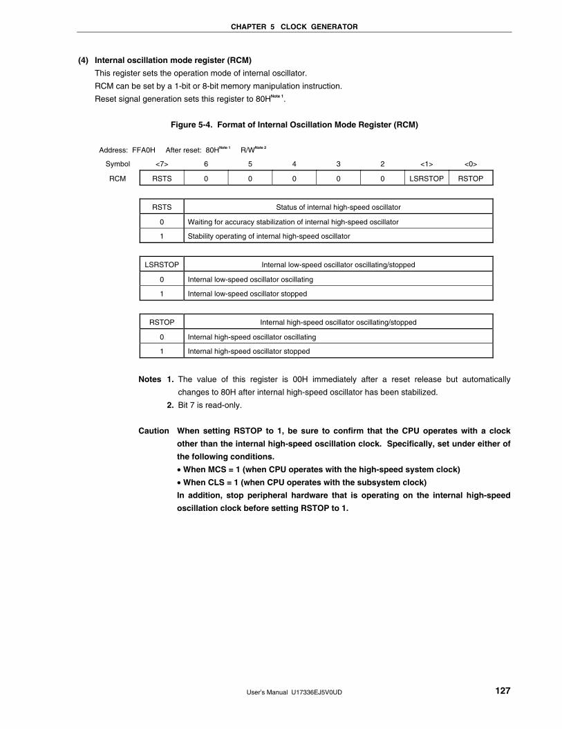
CHAPTER 5 CLOCK GENERATOR
User’s Manual U17336EJ5V0UD 127
(4) Internal oscillation mode register (RCM)
This register sets the operation mode of internal oscillator.
RCM can be set by a 1-bit or 8-bit memory manipulation instruction.
Reset signal generation sets this register to 80HNote 1.
Figure 5-4. Format of Internal Oscillation Mode Register (RCM)
Address: FFA0H After reset: 80HNote 1 R/WNote 2
Symbol <7> 6 5 4 3 2 <1> <0>
RCM RSTS 0 0 0 0 0 LSRSTOP RSTOP
RSTS Status of internal high-speed oscillator
0 Waiting for accuracy stabilization of internal high-speed oscillator
1 Stability operating of internal high-speed oscillator
LSRSTOP Internal low-speed oscillator oscillating/stopped
0 Internal low-speed oscillator oscillating
1 Internal low-speed oscillator stopped
RSTOP Internal high-speed oscillator oscillating/stopped
0 Internal high-speed oscillator oscillating
1 Internal high-speed oscillator stopped
Notes 1. The value of this register is 00H immediately after a reset release but automatically
changes to 80H after internal high-speed oscillator has been stabilized.
2. Bit 7 is read-only.
Caution When setting RSTOP to 1, be sure to confirm that the CPU operates with a clock
other than the internal high-speed oscillation clock. Specifically, set under either of
the following conditions.
• When MCS = 1 (when CPU operates with the high-speed system clock)
• When CLS = 1 (when CPU operates with the subsystem clock)
In addition, stop peripheral hardware that is operating on the internal high-speed
oscillation clock before setting RSTOP to 1.

CHAPTER 5 CLOCK GENERATOR
User’s Manual U17336EJ5V0UD 128
(5) Main OSC control register (MOC)
This register selects the operation mode of the high-speed system clock.
This register is used to stop the X1 oscillator or to disable an external clock input from the EXCLK pin when the
CPU operates with a clock other than the high-speed system clock.
MOC can be set by a 1-bit or 8-bit memory manipulation instruction.
Reset signal generation sets this register to 80H.
Figure 5-5. Format of Main OSC Control Register (MOC)
Address: FFA2H After reset: 80H R/W
Symbol <7> 6 5 4 3 2 1 0
MOC MSTOP 0 0 0 0 0 0 0
Control of high-speed system clock operation
MSTOP
X1 oscillation mode External clock input mode
0 X1 oscillator operating External clock from EXCLK pin is enabled
1 X1 oscillator stopped External clock from EXCLK pin is disabled
Cautions 1. When setting MSTOP to 1, be sure to confirm that the CPU operates with a clock
other than the high-speed system clock. Specifically, set under either of the
following conditions.
• When MCS = 0 (when CPU operates with the internal high-speed oscillation
clock)
• When CLS = 1 (when CPU operates with the subsystem clock)
In addition, stop peripheral hardware that is operating on the high-speed system
clock before setting MSTOP to 1.
2. Do not clear MSTOP to 0 while bit 6 (OSCSEL) of the clock operation mode select
register (OSCCTL) is 0 (I/O port mode).
3. The peripheral hardware cannot operate when the peripheral hardware clock is
stopped. To resume the operation of the peripheral hardware after the peripheral
hardware clock has been stopped, initialize the peripheral hardware.

CHAPTER 5 CLOCK GENERATOR
User’s Manual U17336EJ5V0UD 129
(6) Main clock mode register (MCM)
This register selects the main system clock supplied to CPU clock and clock supplied to peripheral hardware
clock.
MCM can be set by a 1-bit or 8-bit memory manipulation instruction.
Reset signal generation clears this register to 00H.
Figure 5-6. Format of Main Clock Mode Register (MCM)
Address: FFA1H After reset: 00H R/WNote
Symbol 7 6 5 4 3 <2> <1> <0>
MCM 0 0 0 0 0 XSEL MCS MCM0
Selection of clock supplied to main system clock and peripheral hardware
XSEL MCM0
Main system clock (fXP) Peripheral hardware clock (fPRS)
0 0
0 1
Internal high-speed oscillation clock
(fRH)
1 0
Internal high-speed oscillation clock
(fRH)
1 1 High-speed system clock (fXH)
High-speed system clock (fXH)
MCS Main system clock status
0 Operates with internal high-speed oscillation clock
1 Operates with high-speed system clock
Note Bit 1 is read-only.
Cautions 1. XSEL can be changed only once after a reset release.
2. A clock other than fPRS is supplied to the following peripheral functions
regardless of the setting of XSEL and MCM0.
• Watchdog timer (operates with internal low-speed oscillation clock)
• When “fRL”, “fRL/27”, or “fRL/29” is selected as the count clock for 8-bit timer H1
(operates with internal low-speed oscillation clock)
• Peripheral hardware selects the external clock as the clock source
(Except when the external count clock of TM00 is selected (TI000 pin valid
edge))
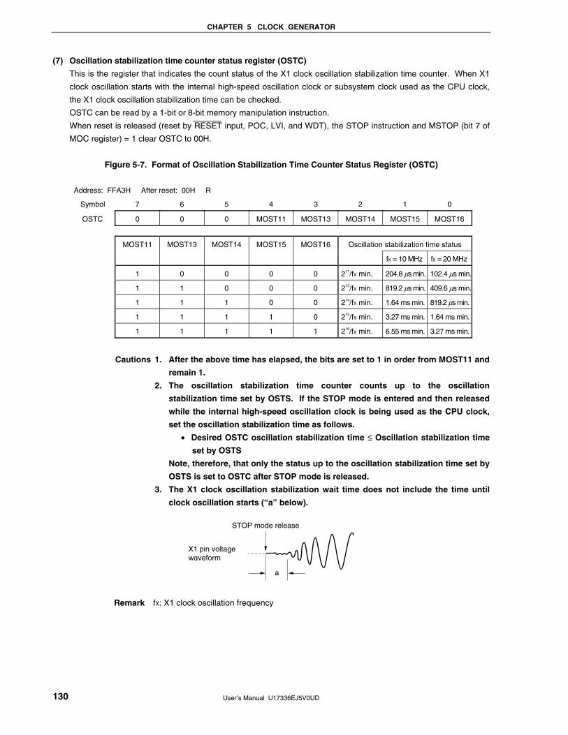
CHAPTER 5 CLOCK GENERATOR
User’s Manual U17336EJ5V0UD 130
(7) Oscillation stabilization time counter status register (OSTC)
This is the register that indicates the count status of the X1 clock oscillation stabilization time counter. When X1
clock oscillation starts with the internal high-speed oscillation clock or subsystem clock used as the CPU clock,
the X1 clock oscillation stabilization time can be checked.
OSTC can be read by a 1-bit or 8-bit memory manipulation instruction.
When reset is released (reset by RESET input, POC, LVI, and WDT), the STOP instruction and MSTOP (bit 7 of
MOC register) = 1 clear OSTC to 00H.
Figure 5-7. Format of Oscillation Stabilization Time Counter Status Register (OSTC)
Address: FFA3H After reset: 00H R
Symbol 7 6 5 4 3 2 1 0
OSTC 0 0 0 MOST11 MOST13 MOST14 MOST15 MOST16
MOST11 MOST13 MOST14 MOST15 MOST16 Oscillation stabilization time status
fX = 10 MHz fX = 20 MHz
1 0 0 0 0 211/fX min. 204.8 μs min. 102.4 μs min.
1 1 0 0 0 213/fX min. 819.2 μs min. 409.6 μs min.
1 1 1 0 0 214/fX min. 1.64 ms min. 819.2 μs min.
1 1 1 1 0 215/fX min. 3.27 ms min. 1.64 ms min.
1 1 1 1 1 216/fX min. 6.55 ms min. 3.27 ms min.
Cautions 1. After the above time has elapsed, the bits are set to 1 in order from MOST11 and
remain 1.
2. The oscillation stabilization time counter counts up to the oscillation
stabilization time set by OSTS. If the STOP mode is entered and then released
while the internal high-speed oscillation clock is being used as the CPU clock,
set the oscillation stabilization time as follows.
• Desired OSTC oscillation stabilization time ≤ Oscillation stabilization time
set by OSTS
Note, therefore, that only the status up to the oscillation stabilization time set by
OSTS is set to OSTC after STOP mode is released.
3. The X1 clock oscillation stabilization wait time does not include the time until
clock oscillation starts (“a” below).
STOP mode release
X1 pin voltage waveform
a
Remark fX: X1 clock oscillation frequency

CHAPTER 5 CLOCK GENERATOR
User’s Manual U17336EJ5V0UD 131
(8) Oscillation stabilization time select register (OSTS)
This register is used to select the X1 clock oscillation stabilization wait time when the STOP mode is released.
When the X1 clock is selected as the CPU clock, the operation waits for the time set using OSTS after the STOP
mode is released.
When the internal high-speed oscillation clock is selected as the CPU clock, confirm with OSTC that the desired
oscillation stabilization time has elapsed after the STOP mode is released. The oscillation stabilization time can
be checked up to the time set using OSTC.
OSTS can be set by an 8-bit memory manipulation instruction.
Reset signal generation sets OSTS to 05H.
Figure 5-8. Format of Oscillation Stabilization Time Select Register (OSTS)
Address: FFA4H After reset: 05H R/W
Symbol 7 6 5 4 3 2 1 0
OSTS 0 0 0 0 0 OSTS2 OSTS1 OSTS0
OSTS2 OSTS1 OSTS0 Oscillation stabilization time selection
fX = 10 MHz fX = 20 MHz
0 0 1 211/fX 204.8 μs 102.4 μs
0 1 0 213/fX 819.2 μs 409.6 μs
0 1 1 214/fX 1.64 ms 819.2 μs
1 0 0 215/fX 3.27 ms 1.64 ms
1 0 1 216/fX 6.55 ms 3.27 ms
Other than above Setting prohibited
Cautions 1. To set the STOP mode when the X1 clock is used as the CPU clock, set OSTS
before executing the STOP instruction.
2. Do not change the value of the OSTS register during the X1 clock oscillation
stabilization time.
3. The oscillation stabilization time counter counts up to the oscillation
stabilization time set by OSTS. If the STOP mode is entered and then released
while the internal high-speed oscillation clock is being used as the CPU clock,
set the oscillation stabilization time as follows.
• Desired OSTC oscillation stabilization time ≤ Oscillation stabilization time
set by OSTS
Note, therefore, that only the status up to the oscillation stabilization time set by
OSTS is set to OSTC after STOP mode is released.
4. The X1 clock oscillation stabilization wait time does not include the time until
clock oscillation starts (“a” below).
STOP mode release
X1 pin voltage waveform
a
Remark fX: X1 clock oscillation frequency

CHAPTER 5 CLOCK GENERATOR
User’s Manual U17336EJ5V0UD 132
5.4 System Clock Oscillator
5.4.1 X1 oscillator
The X1 oscillator oscillates with a crystal resonator or ceramic resonator (1 to 20 MHz) connected to the X1 and X2
pins.
An external clock can also be input. In this case, input the clock signal to the EXCLK pin.
Figure 5-9 shows an example of the external circuit of the X1 oscillator.
Figure 5-9. Example of External Circuit of X1 Oscillator
(a) Crystal or ceramic oscillation (b) External clock
VSS
X1
X2
Crystal resonator or ceramic resonator
EXCLKExternal clock
Cautions are listed on the next page.
5.4.2 XT1 oscillator
The XT1 oscillator oscillates with a crystal resonator (standard: 32.768 kHz) connected to the XT1 and XT2 pins.
An external clock can also be input. In this case, input the clock signal to the EXCLKS pin.
Figure 5-10 shows an example of the external circuit of the XT1 oscillator.
Figure 5-10. Example of External Circuit of XT1 Oscillator
(a) Crystal oscillation (b) External clock
XT2
VSS
XT1
32.768kHz
EXCLKSExternal clock
Cautions are listed on the next page.

CHAPTER 5 CLOCK GENERATOR
User’s Manual U17336EJ5V0UD 133
Caution 1. When using the X1 oscillator and XT1 oscillator, wire as follows in the area enclosed by the
broken lines in the Figures 5-9 and 5-10 to avoid an adverse effect from wiring capacitance.
• Keep the wiring length as short as possible.
• Do not cross the wiring with the other signal lines. Do not route the wiring near a signal
line through which a high fluctuating current flows.
• Always make the ground point of the oscillator capacitor the same potential as VSS. Do
not ground the capacitor to a ground pattern through which a high current flows.
• Do not fetch signals from the oscillator.
Note that the XT1 oscillator is designed as a low-amplitude circuit for reducing power
consumption.
Figure 5-11 shows examples of incorrect resonator connection.
Figure 5-11. Examples of Incorrect Resonator Connection (1/2)
(a) Too long wiring (b) Crossed signal line
X2VSS X1 X1VSS X2
PORT
Remark When using the subsystem clock, replace X1 and X2 with XT1 and XT2, respectively. Also, insert
resistors in series on the XT2 side.

CHAPTER 5 CLOCK GENERATOR
User’s Manual U17336EJ5V0UD 134
Figure 5-11. Examples of Incorrect Resonator Connection (2/2)
(c) Wiring near high alternating current (d) Current flowing through ground line of oscillator
(potential at points A, B, and C fluctuates)
VSS X1 X2
VSS X1 X2
A B C
Pmn
VDD
High current
Hig
h cu
rren
t
(e) Signals are fetched
VSS X1 X2
Remark When using the subsystem clock, replace X1 and X2 with XT1 and XT2, respectively. Also, insert
resistors in series on the XT2 side.
Caution 2. When X2 and XT1 are wired in parallel, the crosstalk noise of X2 may increase with XT1,
resulting in malfunctioning.

CHAPTER 5 CLOCK GENERATOR
User’s Manual U17336EJ5V0UD 135
5.4.3 When subsystem clock is not used
If it is not necessary to use the subsystem clock for low power consumption operations, or if not using the
subsystem clock as an I/O port, set the XT1 and XT2 pins to I/O mode (OSCSELS = 0) and connect them as follows.
Input (PM123/PM124 = 1): Independently connect to VDD or VSS via a resistor.
Output (PM123/PM124 = 0): Leave open.
Remark OSCSELS: Bit 4 of clock operation mode select register (OSCCTL)
PM123, PM124: Bits 3 and 4 of port mode register 12 (PM12)
5.4.4 Internal high-speed oscillator
The internal high-speed oscillator is incorporated in the 78K0/KC2. Oscillation can be controlled by the internal
oscillation mode register (RCM).
After a reset release, the internal high-speed oscillator automatically starts oscillation (8 MHz (TYP.)).
5.4.5 Internal low-speed oscillator
The internal low-speed oscillator is incorporated in the 78K0/KC2.
The internal low-speed oscillation clock is only used as the watchdog timer and the clock of 8-bit timer H1. The
internal low-speed oscillation clock cannot be used as the CPU clock.
“Can be stopped by software” or “Cannot be stopped” can be selected by the option byte. When “Can be stopped
by software” is set, oscillation can be controlled by the internal oscillation mode register (RCM).
After a reset release, the internal low-speed oscillator automatically starts oscillation, and the watchdog timer is
driven (240 kHz (TYP.)) if the watchdog timer operation is enabled using the option byte.
5.4.6 Prescaler
The prescaler generates various clocks by dividing the main system clock when the main system clock is selected
as the clock to be supplied to the CPU.

CHAPTER 5 CLOCK GENERATOR
User’s Manual U17336EJ5V0UD 136
5.5 Clock Generator Operation
The clock generator generates the following clocks and controls the operation modes of the CPU, such as standby
mode (see Figure 5-1).
• Main system clock fXP
• High-speed system clock fXH
X1 clock fX
External main system clock fEXCLK
• Internal high-speed oscillation clock fRH
• Subsystem clock fSUB
• XT1 clock fXT
• External subsystem clock fEXCLKS
• Internal low-speed oscillation clock fRL
• CPU clock fCPU
• Peripheral hardware clock fPRS
The CPU starts operation when the internal high-speed oscillator starts outputting after a reset release in the
78K0/KC2, thus enabling the following.
(1) Enhancement of security function
When the X1 clock is set as the CPU clock by the default setting, the device cannot operate if the X1 clock is
damaged or badly connected and therefore does not operate after reset is released. However, the start clock of
the CPU is the internal high-speed oscillation clock, so the device can be started by the internal high-speed
oscillation clock after a reset release. Consequently, the system can be safely shut down by performing a
minimum operation, such as acknowledging a reset source by software or performing safety processing when
there is a malfunction.
(2) Improvement of performance
Because the CPU can be started without waiting for the X1 clock oscillation stabilization time, the total
performance can be improved.
When the power supply voltage is turned on, the clock generator operation is shown in Figure 5-12.

CHAPTER 5 CLOCK GENERATOR
User’s Manual U17336EJ5V0UD 137
Figure 5-12. Clock Generator Operation When Power Supply Voltage Is Turned On
(When 1.59 V POC Mode Is Set (Option Byte: POCMODE = 0))
Internal high-speed oscillation clock (fRH)
CPU clock
High-speedsystem clock (fXH)
(when X1 oscillationselected)
Internal high-speed oscillation clock High-speed system clock
Switched bysoftware
Subsystem clock (fSUB)(when XT1 oscillation
selected)
Subsystem clock
X1 clockoscillation stabilization time:
211/fX to 216/fXNote 4
Starting X1 oscillation is set by software.
Starting XT1 oscillation is set by software.
Reset processing(11 to 45 s)<3> Waiting for
voltage stabilization
Internal reset signal
0 V
1.59 V (TYP.)
1.8 VNotes 1, 2
0.5 V/ms (MIN.)Notes 1, 2
Power supplyvoltage (VDD)
<1>
<2>
<4>
<5> <5>
<4>
Note 3
(1.93 to 5.39 ms)
μ
<1> When the power is turned on, an internal reset signal is generated by the power-on-clear (POC) circuit.
<2> When the power supply voltage exceeds 1.59 V (TYP.), the reset is released and the internal high-speed
oscillator automatically starts oscillation.
<3> When the power supply voltage rises with a slope of 0.5 V/ms (MIN.), the CPU starts operation on the
internal high-speed oscillation clock after the reset is released and after the stabilization times for the voltage
of the power supply and regulator have elapsed, and then reset processing is performed.
<4> Set the start of oscillation of the X1 or XT1 clock via software (see (1) in 5.6.1 Example of controlling high-
speed system clock and (1) in 5.6.3 Example of controlling subsystem clock).
<5> When switching the CPU clock to the X1 or XT1 clock, wait for the clock oscillation to stabilize, and then set
switching via software (see (3) in 5.6.1 Example of controlling high-speed system clock and (3) in 5.6.3
Example of controlling subsystem clock).
Notes 1. With standard and (A) grade products, if the voltage rises with a slope of less than 0.5 V/ms (MIN.)
from power application until the voltage reaches 1.8 V, input a low level to the RESET pin from power
application until the voltage reaches 1.8 V, or set the 2.7 V/1.59 V POC mode by using the option byte
(POCMODE = 1) (see Figure 5-13). When a low level has been input to the RESET pin until the
voltage reaches 1.8 V, the CPU operates with the same timing as <2> and thereafter in Figure 5-12,
after the reset has been released by the RESET pin.
2. With (A2) grade products, if the voltage rises with a slope of less than 0.75 V/ms (MIN.) from power
application until the voltage reaches 2.7 V, input a low level to the RESET pin from power application
until the voltage reaches 2.7 V. When a low level has been input to the RESET pin until the voltage
reaches 2.7 V, the CPU operates with the same timing as <2> and thereafter in Figure 5-12, after the
reset has been released by the RESET pin.
<R>
<R>

CHAPTER 5 CLOCK GENERATOR
User’s Manual U17336EJ5V0UD 138
Notes 3. The internal voltage stabilization time includes the oscillation accuracy stabilization time of the internal
high-speed oscillation clock.
4. When releasing a reset (above figure) or releasing STOP mode while the CPU is operating on the
internal high-speed oscillation clock, confirm the oscillation stabilization time for the X1 clock using the
oscillation stabilization time counter status register (OSTC). If the CPU operates on the high-speed
system clock (X1 oscillation), set the oscillation stabilization time when releasing STOP mode using the
oscillation stabilization time select register (OSTS).
Caution It is not necessary to wait for the oscillation stabilization time when an external clock input from
the EXCLK and EXCLKS pins is used.
Remark While the microcontroller is operating, a clock that is not used as the CPU clock can be stopped via
software settings. The internal high-speed oscillation clock and high-speed system clock can be
stopped by executing the STOP instruction (see (4) in 5.6.1 Example of controlling high-speed
system clock, (3) in 5.6.2 Example of controlling internal high-speed oscillation clock, and (4) in
5.6.3 Example of controlling subsystem clock).
Figure 5-13. Clock Generator Operation When Power Supply Voltage Is Turned On
(When 2.7 V/1.59 V POC Mode Is Set (Option Byte: POCMODE = 1))
Internal high-speed oscillation clock (fRH)
CPU clock
High-speedsystem clock (fXH)
(when X1 oscillationselected)
Internal high-speedoscillation clock High-speed system clock
Switched bysoftware
Subsystem clock (fSUB)(when XT1 oscillation
selected)
Subsystem clock
X1 clockoscillation stabilization time:
211/fX to 216/fXNote
Starting X1 oscillation is set by software.
Starting XT1 oscillation is set by software.
Waiting for oscillation accuracy stabilization (86 to 361 s)
Internal reset signal
0 V
2.7 V (TYP.) Power supplyvoltage (VDD)
<1>
<3>
<2>
<4>
<5>
Reset processing(11 to 45 s)
<4>
<5>
μ
μ
<1> When the power is turned on, an internal reset signal is generated by the power-on-clear (POC) circuit.
<2> When the power supply voltage exceeds 2.7 V (TYP.), the reset is released and the internal high-speed
oscillator automatically starts oscillation.
<3> After the reset is released and reset processing is performed, the CPU starts operation on the internal high-
speed oscillation clock.
<4> Set the start of oscillation of the X1 or XT1 clock via software (see (1) in 5.6.1 Example of controlling high-
speed system clock and (1) in 5.6.3 Example of controlling subsystem clock).

CHAPTER 5 CLOCK GENERATOR
User’s Manual U17336EJ5V0UD 139
<5> When switching the CPU clock to the X1 or XT1 clock, wait for the clock oscillation to stabilize, and then set
switching via software (see (3) in 5.6.1 Example of controlling high-speed system clock and (3) in 5.6.3
Example of controlling subsystem clock).
Note When releasing a reset (above figure) or releasing STOP mode while the CPU is operating on the internal
high-speed oscillation clock, confirm the oscillation stabilization time for the X1 clock using the oscillation
stabilization time counter status register (OSTC). If the CPU operates on the high-speed system clock (X1
oscillation), set the oscillation stabilization time when releasing STOP mode using the oscillation
stabilization time select register (OSTS).
Cautions 1. A voltage oscillation stabilization time of 1.93 to 5.39 ms is required after the supply voltage
reaches 1.59 V (TYP.). If the supply voltage rises from 1.59 V (TYP.) to 2.7 V (TYP.) within 1.93
ms, the power supply oscillation stabilization time of 0 to 5.39 ms is automatically generated
before reset processing.
2. It is not necessary to wait for the oscillation stabilization time when an external clock input
from the EXCLK and EXCLKS pins is used.
Remark While the microcontroller is operating, a clock that is not used as the CPU clock can be stopped via
software settings. The internal high-speed oscillation clock and high-speed system clock can be
stopped by executing the STOP instruction (see (4) in 5.6.1 Example of controlling high-speed
system clock, (3) in 5.6.2 Example of controlling internal high-speed oscillation clock, and (4) in
5.6.3 Example of controlling subsystem clock).

CHAPTER 5 CLOCK GENERATOR
User’s Manual U17336EJ5V0UD 140
5.6 Controlling Clock
5.6.1 Controlling high-speed system clock
The following two types of high-speed system clocks are available.
• X1 clock: Crystal/ceramic resonator is connected across the X1 and X2 pins.
• External main system clock: External clock is input to the EXCLK pin.
When the high-speed system clock is not used, the X1/P121 and X2/EXCLK/P122 pins can be used as I/O port
pins.
Caution The X1/P121 and X2/EXCLK/P122 pins are in the I/O port mode after a reset release.
The following describes examples of setting procedures for the following cases.
(1) When oscillating X1 clock
(2) When using external main system clock
(3) When using high-speed system clock as CPU clock and peripheral hardware clock
(4) When stopping high-speed system clock
(1) Example of setting procedure when oscillating the X1 clock
<1> Setting frequency (OSCCTL register)
Using AMPH, set the gain of the on-chip oscillator according to the frequency to be used.
AMPHNote Operating Frequency Control
0 1 MHz ≤ fXH ≤ 10 MHz
1 10 MHz < fXH ≤ 20 MHz
Note Set AMPH before setting the peripheral functions after a reset release. The value of AMPH can be changed only once after a reset release. When AMPH is set to 1, the clock supply to the CPU
is stopped for 4.06 to 16.12 μs.
Remark fXH: High-speed system clock frequency
<2> Setting P121/X1 and P122/X2/EXCLK pins and selecting X1 clock or external clock (OSCCTL register)
When EXCLK is cleared to 0 and OSCSEL is set to 1, the mode is switched from port mode to X1
oscillation mode.
EXCLK OSCSEL Operation Mode of High-
Speed System Clock Pin
P121/X1 Pin P122/X2/EXCLK Pin
0 1 X1 oscillation mode Crystal/ceramic resonator connection
<3> Controlling oscillation of X1 clock (MOC register) If MSTOP is cleared to 0, the X1 oscillator starts oscillating.
<4> Waiting for the stabilization of the oscillation of X1 clock
Check the OSTC register and wait for the necessary time.
During the wait time, other software processing can be executed with the internal high-speed oscillation clock.
<R>

CHAPTER 5 CLOCK GENERATOR
User’s Manual U17336EJ5V0UD 141
Cautions 1. Do not change the value of EXCLK and OSCSEL while the X1 clock is operating.
2. Set the X1 clock after the supply voltage has reached the operable voltage of the clock to
be used (see CHAPTER 28 ELECTRICAL SPECIFICATIONS (STANDARD PRODUCTS) to
CHAPTER 31 ELECTRICAL SPECIFICATIONS ((A2) GRADE PRODUCTS: TA = −40 to
+125°C)).
(2) Example of setting procedure when using the external main system clock
<1> Setting frequency (OSCCTL register)
Using AMPH, set the frequency to be used.
AMPHNote Operating Frequency Control
0 1 MHz ≤ fXH ≤ 10 MHz
1 10 MHz < fXH ≤ 20 MHz
Note Set AMPH before setting the peripheral functions after a reset release. The value of AMPH can be changed only once after a reset release. The clock supply to the CPU is stopped for the
duration of 160 external clocks after AMPH is set to 1.
Remark fXH: High-speed system clock frequency
<2> Setting P121/X1 and P122/X2/EXCLK pins and selecting operation mode (OSCCTL register)
When EXCLK and OSCSEL are set to 1, the mode is switched from port mode to external clock input
mode.
EXCLK OSCSEL Operation Mode of High-
Speed System Clock Pin
P121/X1 Pin P122/X2/EXCLK Pin
1 1 External clock input mode I/O port External clock input
<3> Controlling external main system clock input (MOC register) When MSTOP is cleared to 0, the input of the external main system clock is enabled.
Cautions 1. Do not change the value of EXCLK and OSCSEL while the external main system clock is
operating.
2. Set the external main system clock after the supply voltage has reached the operable
voltage of the clock to be used (see CHAPTER 28 ELECTRICAL SPECIFICATIONS
(STANDARD PRODUCTS) to CHAPTER 31 ELECTRICAL SPECIFICATIONS ((A2) GRADE
PRODUCTS: TA = −40 to +125°C)).
(3) Example of setting procedure when using high-speed system clock as CPU clock and peripheral
hardware clock
<1> Setting high-speed system clock oscillationNote
(See 5.6.1 (1) Example of setting procedure when oscillating the X1 clock and (2) Example of
setting procedure when using the external main system clock.)
Note The setting of <1> is not necessary when high-speed system clock is already operating.

CHAPTER 5 CLOCK GENERATOR
User’s Manual U17336EJ5V0UD 142
<2> Setting the high-speed system clock as the main system clock (MCM register)
When XSEL and MCM0 are set to 1, the high-speed system clock is supplied as the main system clock
and peripheral hardware clock.
Selection of Main System Clock and Clock Supplied to Peripheral Hardware XSEL MCM0
Main System Clock (fXP) Peripheral Hardware Clock (fPRS)
1 1 High-speed system clock (fXH) High-speed system clock (fXH)
Caution If the high-speed system clock is selected as the main system clock, a clock other than
the high-speed system clock cannot be set as the peripheral hardware clock.
<3> Setting the main system clock as the CPU clock and selecting the division ratio (PCC register)
When CSS is cleared to 0, the main system clock is supplied to the CPU. To select the CPU clock
division ratio, use PCC0, PCC1, and PCC2.
CSS PCC2 PCC1 PCC0 CPU Clock (fCPU) Selection
0 0 0 fXP
0 0 1 fXP/2 (default)
0 1 0 fXP/22
0 1 1 fXP/23
1 0 0 fXP/24
0
Other than above Setting prohibited
(4) Example of setting procedure when stopping the high-speed system clock
The high-speed system clock can be stopped in the following two ways.
• Executing the STOP instruction and stopping the X1 oscillation (disabling clock input if the external clock is
used)
• Setting MSTOP to 1 and stopping the X1 oscillation (disabling clock input if the external clock is used)
(a) To execute a STOP instruction
<1> Setting to stop peripheral hardware
Stop peripheral hardware that cannot be used in the STOP mode (for peripheral hardware that
cannot be used in STOP mode, see CHAPTER 20 STANDBY FUNCTION).
<2> Setting the X1 clock oscillation stabilization time after standby release
When the CPU is operating on the X1 clock, set the value of the OSTS register before the STOP
instruction is executed.
<3> Executing the STOP instruction
When the STOP instruction is executed, the system is placed in the STOP mode and X1 oscillation
is stopped (the input of the external clock is disabled).

CHAPTER 5 CLOCK GENERATOR
User’s Manual U17336EJ5V0UD 143
(b) To stop X1 oscillation (disabling external clock input) by setting MSTOP to 1
<1> Confirming the CPU clock status (PCC and MCM registers)
Confirm with CLS and MCS that the CPU is operating on a clock other than the high-speed system
clock.
When CLS = 0 and MCS = 1, the high-speed system clock is supplied to the CPU, so change the
CPU clock to the subsystem clock or internal high-speed oscillation clock.
CLS MCS CPU Clock Status
0 0 Internal high-speed oscillation clock
0 1 High-speed system clock
1 × Subsystem clock
<2> Stopping the high-speed system clock (MOC register)
When MSTOP is set to 1, X1 oscillation is stopped (the input of the external clock is disabled).
Caution Be sure to confirm that MCS = 0 or CLS = 1 when setting MSTOP to 1. In addition, stop
peripheral hardware that is operating on the high-speed system clock.
5.6.2 Example of controlling internal high-speed oscillation clock
The following describes examples of clock setting procedures for the following cases.
(1) When restarting oscillation of the internal high-speed oscillation clock
(2) When using internal high-speed oscillation clock as CPU clock, and internal high-speed oscillation clock or
high-speed system clock as peripheral hardware clock
(3) When stopping the internal high-speed oscillation clock
(1) Example of setting procedure when restarting oscillation of the internal high-speed oscillation clockNote 1
<1> Setting restart of oscillation of the internal high-speed oscillation clock (RCM register)
When RSTOP is cleared to 0, the internal high-speed oscillation clock starts operating.
<2> Waiting for the oscillation accuracy stabilization time of internal high-speed oscillation clock (RCM
register)
Wait until RSTS is set to 1Note 2.
Notes 1. After a reset release, the internal high-speed oscillator automatically starts oscillating and the
internal high-speed oscillation clock is selected as the CPU clock.
2. This wait time is not necessary if high accuracy is not necessary for the CPU clock and peripheral
hardware clock.
(2) Example of setting procedure when using internal high-speed oscillation clock as CPU clock, and
internal high-speed oscillation clock or high-speed system clock as peripheral hardware clock
<1> • Restarting oscillation of the internal high-speed oscillation clockNote
(See 5.6.2 (1) Example of setting procedure when restarting internal high-speed oscillation
clock).
• Oscillating the high-speed system clockNote
(This setting is required when using the high-speed system clock as the peripheral hardware clock.
See 5.6.1 (1) Example of setting procedure when oscillating the X1 clock and (2) Example of
setting procedure when using the external main system clock.)

CHAPTER 5 CLOCK GENERATOR
User’s Manual U17336EJ5V0UD 144
Note The setting of <1> is not necessary when the internal high-speed oscillation clock or high-
speed system clock is already operating.
<2> Selecting the clock supplied as the main system clock and peripheral hardware clock (MCM register)
Set the main system clock and peripheral hardware clock using XSEL and MCM0.
Selection of Main System Clock and Clock Supplied to Peripheral Hardware XSEL MCM0
Main System Clock (fXP) Peripheral Hardware Clock (fPRS)
0 0
0 1
Internal high-speed oscillation clock (fRH)
1 0
Internal high-speed oscillation clock (fRH)
High-speed system clock (fXH)
<3> Selecting the CPU clock division ratio (PCC register)
When CSS is cleared to 0, the main system clock is supplied to the CPU. To select the CPU clock
division ratio, use PCC0, PCC1, and PCC2.
CSS PCC2 PCC1 PCC0 CPU Clock (fCPU) Selection
0 0 0 fXP
0 0 1 fXP/2 (default)
0 1 0 fXP/22
0 1 1 fXP/23
1 0 0 fXP/24
0
Other than above Setting prohibited
(3) Example of setting procedure when stopping the internal high-speed oscillation clock
The internal high-speed oscillation clock can be stopped in the following two ways.
• Executing the STOP instruction to set the STOP mode
• Setting RSTOP to 1 and stopping the internal high-speed oscillation clock
(a) To execute a STOP instruction
<1> Setting of peripheral hardware
Stop peripheral hardware that cannot be used in the STOP mode (for peripheral hardware that
cannot be used in STOP mode, see CHAPTER 20 STANDBY FUNCTION).
<2> Setting the X1 clock oscillation stabilization time after standby release
When the CPU is operating on the X1 clock, set the value of the OSTS register before the STOP
instruction is executed.
<3> Executing the STOP instruction
When the STOP instruction is executed, the system is placed in the STOP mode and internal high-
speed oscillation clock is stopped.

CHAPTER 5 CLOCK GENERATOR
User’s Manual U17336EJ5V0UD 145
(b) To stop internal high-speed oscillation clock by setting RSTOP to 1
<1> Confirming the CPU clock status (PCC and MCM registers)
Confirm with CLS and MCS that the CPU is operating on a clock other than the internal high-speed
oscillation clock.
When CLS = 0 and MCS = 0, the internal high-speed oscillation clock is supplied to the CPU, so
change the CPU clock to the high-speed system clock or subsystem clock.
CLS MCS CPU Clock Status
0 0 Internal high-speed oscillation clock
0 1 High-speed system clock
1 × Subsystem clock
<2> Stopping the internal high-speed oscillation clock (RCM register)
When RSTOP is set to 1, internal high-speed oscillation clock is stopped.
Caution Be sure to confirm that MCS = 1 or CLS = 1 when setting RSTOP to 1. In addition, stop
peripheral hardware that is operating on the internal high-speed oscillation clock.
5.6.3 Example of controlling subsystem clock
The following two types of subsystem clocks are available.
• XT1 clock: Crystal/ceramic resonator is connected across the XT1 and XT2 pins.
• External subsystem clock: External clock is input to the EXCLKS pin.
When the subsystem clock is not used, the XT1/P123 and XT2/EXCLKS/P124 pins can be used as I/O port pins.
Caution The XT1/P123 and XT2/EXCLKS/P124 pins are in the I/O port mode after a reset release.
The following describes examples of setting procedures for the following cases.
(1) When oscillating XT1 clock
(2) When using external subsystem clock
(3) When using subsystem clock as CPU clock
(4) When stopping subsystem clock
(1) Example of setting procedure when oscillating the XT1 clock
<1> Setting XT1 and XT2 pins and selecting operation mode (PCC and OSCCTL registers)
When XTSTART, EXCLKS, and OSCSELS are set as any of the following, the mode is switched from
port mode to XT1 oscillation mode.
XTSTART EXCLKS OSCSELS Operation Mode of
Subsystem Clock Pin
P123/XT1 Pin P124/XT2/
EXCLKS Pin
0 0 1
1 × ×
XT1 oscillation mode Crystal/ceramic resonator connection
Remark ×: don’t care
<2> Waiting for the stabilization of the subsystem clock oscillation
Wait for the oscillation stabilization time of the subsystem clock by software, using a timer function.
Caution Do not change the value of XTSTART, EXCLKS, and OSCSELS while the subsystem clock is
operating.
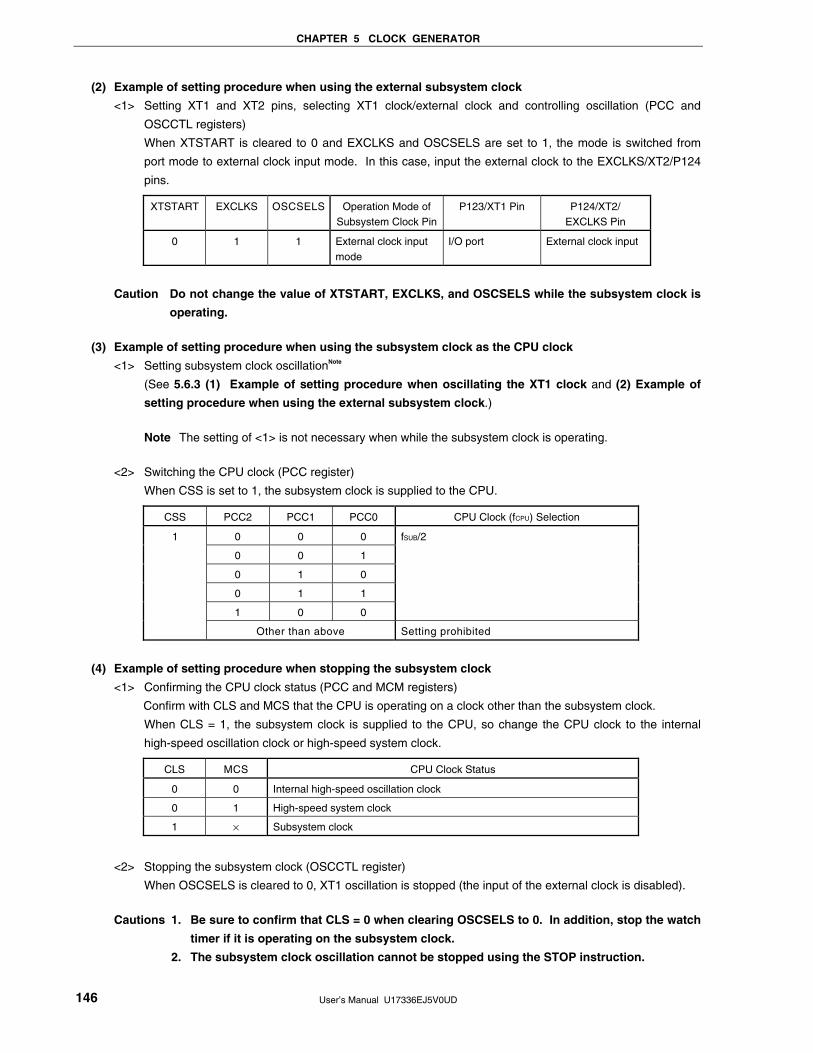
CHAPTER 5 CLOCK GENERATOR
User’s Manual U17336EJ5V0UD 146
(2) Example of setting procedure when using the external subsystem clock
<1> Setting XT1 and XT2 pins, selecting XT1 clock/external clock and controlling oscillation (PCC and
OSCCTL registers)
When XTSTART is cleared to 0 and EXCLKS and OSCSELS are set to 1, the mode is switched from
port mode to external clock input mode. In this case, input the external clock to the EXCLKS/XT2/P124
pins.
XTSTART EXCLKS OSCSELS Operation Mode of Subsystem Clock Pin
P123/XT1 Pin P124/XT2/ EXCLKS Pin
0 1 1 External clock input mode
I/O port External clock input
Caution Do not change the value of XTSTART, EXCLKS, and OSCSELS while the subsystem clock is
operating.
(3) Example of setting procedure when using the subsystem clock as the CPU clock
<1> Setting subsystem clock oscillationNote
(See 5.6.3 (1) Example of setting procedure when oscillating the XT1 clock and (2) Example of
setting procedure when using the external subsystem clock.)
Note The setting of <1> is not necessary when while the subsystem clock is operating.
<2> Switching the CPU clock (PCC register)
When CSS is set to 1, the subsystem clock is supplied to the CPU.
CSS PCC2 PCC1 PCC0 CPU Clock (fCPU) Selection
0 0 0
0 0 1
0 1 0
0 1 1
1 0 0
fSUB/2 1
Other than above Setting prohibited
(4) Example of setting procedure when stopping the subsystem clock
<1> Confirming the CPU clock status (PCC and MCM registers)
Confirm with CLS and MCS that the CPU is operating on a clock other than the subsystem clock.
When CLS = 1, the subsystem clock is supplied to the CPU, so change the CPU clock to the internal
high-speed oscillation clock or high-speed system clock.
CLS MCS CPU Clock Status
0 0 Internal high-speed oscillation clock
0 1 High-speed system clock
1 × Subsystem clock
<2> Stopping the subsystem clock (OSCCTL register)
When OSCSELS is cleared to 0, XT1 oscillation is stopped (the input of the external clock is disabled).
Cautions 1. Be sure to confirm that CLS = 0 when clearing OSCSELS to 0. In addition, stop the watch
timer if it is operating on the subsystem clock.
2. The subsystem clock oscillation cannot be stopped using the STOP instruction.

CHAPTER 5 CLOCK GENERATOR
User’s Manual U17336EJ5V0UD 147
5.6.4 Example of controlling internal low-speed oscillation clock
The internal low-speed oscillation clock cannot be used as the CPU clock.
Only the following peripheral hardware can operate with this clock.
• Watchdog timer
• 8-bit timer H1 (if fRL is selected as the count clock)
In addition, the following operation modes can be selected by the option byte.
• Internal low-speed oscillator cannot be stopped
• Internal low-speed oscillator can be stopped by software
The internal low-speed oscillator automatically starts oscillation after a reset release, and the watchdog timer is
driven (240 kHz (TYP.)) if the watchdog timer operation has been enabled by the option byte.
(1) Example of setting procedure when stopping the internal low-speed oscillation clock
<1> Setting LSRSTOP to 1 (RCM register)
When LSRSTOP is set to 1, the internal low-speed oscillation clock is stopped.
(2) Example of setting procedure when restarting oscillation of the internal low-speed oscillation clock
<1> Clearing LSRSTOP to 0 (RCM register)
When LSRSTOP is cleared to 0, the internal low-speed oscillation clock is restarted.
Caution If “Internal low-speed oscillator cannot be stopped” is selected by the option byte, oscillation of
the internal low-speed oscillation clock cannot be controlled.
5.6.5 Clocks supplied to CPU and peripheral hardware
The following table shows the relation among the clocks supplied to the CPU and peripheral hardware, and setting
of registers.
Table 5-4. Clocks Supplied to CPU and Peripheral Hardware, and Register Setting
Supplied Clock
Clock Supplied to CPU Clock Supplied to Peripheral Hardware
XSEL CSS MCM0 EXCLK
Internal high-speed oscillation clock 0 0 × ×
X1 clock 1 0 0 0 Internal high-speed oscillation clock
External main system clock 1 0 0 1
X1 clock 1 0 1 0
External main system clock 1 0 1 1
Internal high-speed oscillation clock 0 1 × ×
1 1 0 0 X1 clock
1 1 1 0
1 1 0 1
Subsystem clock
External main system clock
1 1 1 1
Remarks 1. XSEL: Bit 2 of the main clock mode register (MCM)
2. CSS: Bit 4 of the processor clock control register (PCC)
3. MCM0: Bit 0 of MCM
4. EXCLK: Bit 7 of the clock operation mode select register (OSCCTL)
5. ×: don’t care

CHAPTER 5 CLOCK GENERATOR
User’s Manual U17336EJ5V0UD 148
5.6.6 CPU clock status transition diagram
Figure 5-14 shows the CPU clock status transition diagram of this product.
Figure 5-14. CPU Clock Status Transition Diagram
(When 1.59 V POC Mode Is Set (Option Byte: POCMODE = 0))
Power ON
Reset releaseVDD ≥ 1.59 V (TYP.)
VDD ≥ 1.8 V (MIN.)Note
VDD < 1.59 V (TYP.)
Internal low-speed oscillation: Woken upInternal high-speed oscillation: Woken upX1 oscillation/EXCLK input: Stops (I/O port mode)XT1 oscillation/EXCLKS input: Stops (I/O port mode)
Internal low-speed oscillation: OperatingInternal high-speed oscillation: OperatingX1 oscillation/EXCLK input: Stops (I/O port mode)XT1 oscillation/EXCLKS input: Stops (I/O port mode)
CPU: Operatingwith internal high-speed oscillation
Internal low-speed oscillation: OperableInternal high-speed oscillation: OperatingX1 oscillation/EXCLK input: Selectable by CPUXT1 oscillation/EXCLKS input: Selectable by CPU
CPU: Internal high-speed oscillation
→ STOP
Internal low-speed oscillation: OperableInternal high-speed oscillation: StopsX1 oscillation/EXCLK input: StopsXT1 oscillation/EXCLKS input: Operable
CPU: Internal high-speed oscillation
→ HALT
Internal low-speed oscillation: OperableInternal high-speed oscillation: OperatingX1 oscillation/EXCLK input: OperableXT1 oscillation/EXCLKS input: Operable
CPU: Operatingwith X1 oscillation or
EXCLK input
CPU: X1oscillation/EXCLK
input → STOPCPU: X1
oscillation/EXCLKinput → HALT
Internal low-speed oscillation: OperableInternal high-speed oscillation: Selectable by CPUX1 oscillation/EXCLK input: OperatingXT1 oscillation/EXCLKS input: Selectable by CPU Internal low-speed oscillation:
OperableInternal high-speed oscillation: StopsX1 oscillation/EXCLK input: StopsXT1 oscillation: OperableInternal low-speed oscillation:
OperableInternal high-speed oscillation: OperableX1 oscillation/EXCLK input: OperatingXT1 oscillation/EXCLKS input: Operable
CPU: Operatingwith XT1 oscillation or
EXCLKS input
CPU: XT1oscillation/EXCLKS
input → HALT
Internal low-speed oscillation: OperableInternal high-speed oscillation: Selectable by CPUX1 oscillation/EXCLK input: Selectable by CPUXT1 oscillation/EXCLKS input: Operating
Internal low-speed oscillation: OperableInternal high-speed oscillation: OperableX1 oscillation/EXCLK input: OperableXT1 oscillation/EXCLKS input: Operating
(B)
(A)
(C)
(D)
(E)
(F)
(G)
(H)
(I)
Note 1.8 V (Standard and (A) grade products), 2.7 V ((A2) grade products)
Remark In the 2.7 V/1.59 V POC mode (option byte: POCMODE = 1), the CPU clock status changes to (A) in the
above figure when the supply voltage exceeds 2.7 V (TYP.), and to (B) after reset processing (11 to
45 μs).
<R>

CHAPTER 5 CLOCK GENERATOR
User’s Manual U17336EJ5V0UD 149
Table 5-5 shows transition of the CPU clock and examples of setting the SFR registers.
Table 5-5. CPU Clock Transition and SFR Register Setting Examples (1/4)
(1) CPU operating with internal high-speed oscillation clock (B) after reset release (A)
Status Transition SFR Register Setting
(A) → (B) SFR registers do not have to be set (default status after reset release).
(2) CPU operating with high-speed system clock (C) after reset release (A)
(The CPU operates with the internal high-speed oscillation clock immediately after a reset release (B).)
(Setting sequence of SFR registers)
Setting Flag of SFR Register
Status Transition
AMPH EXCLK OSCSEL MSTOP OSTC
Register
XSEL MCM0
(A) → (B) → (C) (X1 clock: 1 MHz ≤ fXH ≤
10 MHz)
0 0 1 0 Must be
checked
1 1
(A) → (B) → (C) (external main clock: 1 MHz ≤
fXH ≤ 10 MHz)
0 1 1 0 Must not be
checked
1 1
(A) → (B) → (C) (X1 clock: 10 MHz < fXH ≤
20 MHz)
1 0 1 0 Must be
checked
1 1
(A) → (B) → (C) (external main clock: 10 MHz <
fXH ≤ 20 MHz)
1 1 1 0 Must not be
checked
1 1
Caution Set the clock after the supply voltage has reached the operable voltage of the clock to be set (see
CHAPTER 28 ELECTRICAL SPECIFICATIONS (STANDARD PRODUCTS) to CHAPTER 31
ELECTRICAL SPECIFICATIONS ((A2) GRADE PRODUCTS: TA = −40 to +125°C)).
(3) CPU operating with subsystem clock (D) after reset release (A)
(The CPU operates with the internal high-speed oscillation clock immediately after a reset release (B).)
(Setting sequence of SFR registers)
Setting Flag of SFR Register
Status Transition
XTSTART EXCLKS OSCSELS Waiting for
Oscillation
Stabilization
CSS
0 0 1 (A) → (B) → (D) (XT1 clock)
1 × ×
Necessary 1
(A) → (B) → (D) (external subsystem clock) 0 1 1 Unnecessary 1
Remarks 1. (A) to (I) in Table 5-5 correspond to (A) to (I) in Figure 5-14.
2. EXCLK, OSCSEL, EXCLKS, OSCSELS, AMPH:
Bits 7 to 4 and 0 of the clock operation mode select register (OSCCTL)
MSTOP: Bit 7 of the main OSC control register (MOC)
XSEL, MCM0: Bits 2 and 0 of the main clock mode register (MCM)
XTSTART, CSS: Bits 6 and 4 of the processor clock control register (PCC)
×: Don’t care

CHAPTER 5 CLOCK GENERATOR
User’s Manual U17336EJ5V0UD 150
Table 5-5. CPU Clock Transition and SFR Register Setting Examples (2/4)
(4) CPU clock changing from internal high-speed oscillation clock (B) to high-speed system clock (C)
(Setting sequence of SFR registers)
Setting Flag of SFR Register
Status Transition
AMPHNote EXCLK OSCSEL MSTOP OSTC
Register
XSELNote MCM0
(B) → (C) (X1 clock: 1 MHz ≤ fXH ≤ 10 MHz) 0 0 1 0 Must be
checked
1 1
(B) → (C) (external main clock: 1 MHz ≤ fXH ≤
10 MHz)
0 1 1 0 Must not be
checked
1 1
(B) → (C) (X1 clock: 10 MHz < fXH ≤ 20 MHz) 1 0 1 0 Must be
checked
1 1
(B) → (C) (external main clock: 10 MHz < fXH ≤
20 MHz)
1 1 1 0 Must not be
checked
1 1
Unnecessary if these registers
are already set
Unnecessary if the
CPU is operating
with the high-speed
system clock
Note The value of this flag can be changed only once after a reset release. This setting is not necessary if it has
already been set.
Caution Set the clock after the supply voltage has reached the operable voltage of the clock to be set (see
CHAPTER 28 ELECTRICAL SPECIFICATIONS (STANDARD PRODUCTS) to CHAPTER 31
ELECTRICAL SPECIFICATIONS ((A2) GRADE PRODUCTS: TA = −40 to +125°C)).
(5) CPU clock changing from internal high-speed oscillation clock (B) to subsystem clock (D)
(Setting sequence of SFR registers)
Setting Flag of SFR Register
Status Transition
XTSTART EXCLKS OSCSELS Waiting for
Oscillation
Stabilization
CSS
0 0 1 (B) → (D) (XT1 clock)
1 × ×
Necessary 1
(B) → (D) (external subsystem clock) 0 1 1 Unnecessary 1
Unnecessary if the CPU is operating
with the subsystem clock
Remarks 1. (A) to (I) in Table 5-5 correspond to (A) to (I) in Figure 5-14.
2. EXCLK, OSCSEL, EXCLKS, OSCSELS, AMPH:
Bits 7 to 4 and 0 of the clock operation mode select register (OSCCTL)
MSTOP: Bit 7 of the main OSC control register (MOC)
XSEL, MCM0: Bits 2 and 0 of the main clock mode register (MCM)
XTSTART, CSS: Bits 6 and 4 of the processor clock control register (PCC)
×: Don’t care

CHAPTER 5 CLOCK GENERATOR
User’s Manual U17336EJ5V0UD 151
Table 5-5. CPU Clock Transition and SFR Register Setting Examples (3/4)
(6) CPU clock changing from high-speed system clock (C) to internal high-speed oscillation clock (B)
(Setting sequence of SFR registers)
Setting Flag of SFR Register
Status Transition
RSTOP RSTS MCM0
(C) → (B) 0 Confirm this flag is 1. 0
Unnecessary if the CPU is operating
with the internal high-speed oscillation clock
(7) CPU clock changing from high-speed system clock (C) to subsystem clock (D)
(Setting sequence of SFR registers)
Setting Flag of SFR Register
Status Transition
XTSTART EXCLKS OSCSELS Waiting for
Oscillation
Stabilization
CSS
0 0 1 (C) → (D) (XT1 clock)
1 × ×
Necessary 1
(C) → (D) (external subsystem clock) 0 1 1 Unnecessary 1
Unnecessary if the CPU is operating
with the subsystem clock
(8) CPU clock changing from subsystem clock (D) to internal high-speed oscillation clock (B)
(Setting sequence of SFR registers)
Setting Flag of SFR Register
Status Transition
RSTOP RSTS MCM0 CSS
(D) → (B) 0 Confirm this flag
is 1.
0 0
Unnecessary if the CPU is operating
with the internal high-speed
oscillation clock
↑
Unnecessary if
XSEL is 0
Remarks 1. (A) to (I) in Table 5-5 correspond to (A) to (I) in Figure 5-14.
2. MCM0: Bit 0 of the main clock mode register (MCM)
EXCLKS, OSCSELS: Bits 5 and 4 of the clock operation mode select register (OSCCTL)
RSTS, RSTOP: Bits 7 and 0 of the internal oscillation mode register (RCM)
XTSTART, CSS: Bits 6 and 4 of the processor clock control register (PCC)
×: Don’t care


CHAPTER 5 CLOCK GENERATOR
User’s Manual U17336EJ5V0UD 153
5.6.7 Condition before changing CPU clock and processing after changing CPU clock
Condition before changing the CPU clock and processing after changing the CPU clock are shown below.
Table 5-6. Changing CPU Clock
CPU Clock
Before Change After Change
Condition Before Change Processing After Change
X1 clock Stabilization of X1 oscillation
• MSTOP = 0, OSCSEL = 1, EXCLK = 0
• After elapse of oscillation stabilization time
• Internal high-speed oscillator can be
stopped (RSTOP = 1).
• Clock supply to CPU is stopped for 4.06
to 16.12 μs after AMPH has been set to 1.
Internal high-
speed oscillation
clock
External main
system clock
Enabling input of external clock from EXCLK
pin
• MSTOP = 0, OSCSEL = 1, EXCLK = 1
• Internal high-speed oscillator can be
stopped (RSTOP = 1).
• Clock supply to CPU is stopped for the
duration of 160 external clocks from the
EXCLK pin after AMPH has been set to 1.
X1 clock X1 oscillation can be stopped (MSTOP = 1).
External main
system clock
Internal high-
speed oscillation
clock
Oscillation of internal high-speed oscillator
• RSTOP = 0 External main system clock input can be
disabled (MSTOP = 1).
Internal high-
speed oscillation
clock
Operating current can be reduced by
stopping internal high-speed oscillator
(RSTOP = 1).
X1 clock X1 oscillation can be stopped (MSTOP = 1).
External main
system clock
XT1 clock Stabilization of XT1 oscillation
• XTSTART = 0, EXCLKS = 0,
OSCSELS = 1, or XTSTART = 1
• After elapse of oscillation stabilization time
External main system clock input can be
disabled (MSTOP = 1).
Internal high-
speed oscillation
clock
Operating current can be reduced by
stopping internal high-speed oscillator
(RSTOP = 1).
X1 clock X1 oscillation can be stopped (MSTOP = 1).
External main
system clock
External
subsystem clock
Enabling input of external clock from
EXCLKS pin
• XTSTART = 0, EXCLKS = 1,
OSCSELS = 1
External main system clock input can be
disabled (MSTOP = 1).
Internal high-
speed oscillation
clock
Oscillation of internal high-speed oscillator
and selection of internal high-speed
oscillation clock as main system clock
• RSTOP = 0, MCS = 0
XT1 oscillation can be stopped or external
subsystem clock input can be disabled
(OSCSELS = 0).
X1 clock Stabilization of X1 oscillation and selection
of high-speed system clock as main system
clock
• MSTOP = 0, OSCSEL = 1, EXCLK = 0
• After elapse of oscillation stabilization time
• MCS = 1
• XT1 oscillation can be stopped or external
subsystem clock input can be disabled
(OSCSELS = 0).
• Clock supply to CPU is stopped for 4.06
to 16.12 μs after AMPH has been set to 1.
XT1 clock,
external
subsystem clock
External main
system clock
Enabling input of external clock from EXCLK
pin and selection of high-speed system
clock as main system clock
• MSTOP = 0, OSCSEL = 1, EXCLK = 1
• MCS = 1
• XT1 oscillation can be stopped or external
subsystem clock input can be disabled
(OSCSELS = 0).
• Clock supply to CPU is stopped for the
duration of 160 external clocks from the
EXCLK pin after AMPH has been set to 1.
<R>
<R>

CHAPTER 5 CLOCK GENERATOR
User’s Manual U17336EJ5V0UD 154
5.6.8 Time required for switchover of CPU clock and main system clock
By setting bits 0 to 2 (PCC0 to PCC2) and bit 4 (CSS) of the processor clock control register (PCC), the CPU clock
can be switched (between the main system clock and the subsystem clock) and the division ratio of the main system
clock can be changed.
The actual switchover operation is not performed immediately after rewriting to PCC; operation continues on the
pre-switchover clock for several clocks (see Table 5-7).
Whether the CPU is operating on the main system clock or the subsystem clock can be ascertained using bit 5
(CLS) of the PCC register.
Table 5-7. Time Required for Switchover of CPU Clock and Main System Clock Cycle Division Factor
Set Value Before
Switchover
Set Value After Switchover
CSS PCC2 PCC1 PCC0 CSS PCC2 PCC1 PCC0 CSS PCC2 PCC1 PCC0 CSS PCC2 PCC1 PCC0 CSS PCC2 PCC1 PCC0 CSS PCC2 PCC1 PCC0CSS PCC2 PCC1 PCC0
0 0 0 0 0 0 0 1 0 0 1 0 0 0 1 1 0 1 0 0 1 × × ×
0 0 0 16 clocks 16 clocks 16 clocks 16 clocks 2fXP/fSUB clocks
0 0 1 8 clocks 8 clocks 8 clocks 8 clocks fXP/fSUB clocks
0 1 0 4 clocks 4 clocks 4 clocks 4 clocks fXP/2fSUB clocks
0 1 1 2 clocks 2 clocks 2 clocks 2 clocks fXP/4fSUB clocks
0
1 0 0 1 clock 1 clock 1 clock 1 clock fXP/8fSUB clocks
1 × × × 2 clocks 2 clocks 2 clocks 2 clocks 2 clocks
Caution Selection of the main system clock cycle division factor (PCC0 to PCC2) and switchover from the
main system clock to the subsystem clock (changing CSS from 0 to 1) should not be set
simultaneously.
Simultaneous setting is possible, however, for selection of the main system clock cycle division
factor (PCC0 to PCC2) and switchover from the subsystem clock to the main system clock
(changing CSS from 1 to 0).
Remarks 1. The number of clocks listed in Table 5-7 is the number of CPU clocks before switchover.
2. When switching the CPU clock from the main system clock to the subsystem clock, calculate the
number of clocks by rounding up to the next clock and discarding the decimal portion, as shown
below.
Example When switching CPU clock from fXP/2 to fSUB/2 (@ oscillation with fXP = 10 MHz, fSUB =
32.768 kHz)
fXP/fSUB = 10000/32.768 ≅ 305.1 → 306 clocks
By setting bit 0 (MCM0) of the main clock mode register (MCM), the main system clock can be switched (between
the internal high-speed oscillation clock and the high-speed system clock).
The actual switchover operation is not performed immediately after rewriting to MCM0; operation continues on the
pre-switchover clock for several clocks (see Table 5-8).
Whether the CPU is operating on the internal high-speed oscillation clock or the high-speed system clock can be
ascertained using bit 1 (MCS) of MCM.

CHAPTER 5 CLOCK GENERATOR
User’s Manual U17336EJ5V0UD 155
Table 5-8. Maximum Time Required for Main System Clock Switchover
Set Value Before Switchover Set Value After Switchover
MCM0 MCM0
0 1
0 1 + 2fRH/fXH clock
1 1 + 2fXH/fRH clock
Caution When switching the internal high-speed oscillation clock to the high-speed system clock, bit 2
(XSEL) of MCM must be set to 1 in advance. The value of XSEL can be changed only once after a
reset release.
Remarks 1. The number of clocks listed in Table 5-8 is the number of main system clocks before switchover.
2. Calculate the number of clocks in Table 5-8 by removing the decimal portion.
Example When switching the main system clock from the internal high-speed oscillation clock to the
high-speed system clock (@ oscillation with fRH = 8 MHz, fXH = 10 MHz)
1 + 2fRH/fXH = 1 + 2 × 8/10 = 1 + 2 × 0.8 = 1 + 1.6 = 2.6 → 2 clocks
5.6.9 Conditions before clock oscillation is stopped
The following lists the register flag settings for stopping the clock oscillation (disabling external clock input) and
conditions before the clock oscillation is stopped.
Table 5-9. Conditions Before the Clock Oscillation Is Stopped and Flag Settings
Clock Conditions Before Clock Oscillation Is Stopped
(External Clock Input Disabled)
Flag Settings of SFR
Register
Internal high-speed
oscillation clock
MCS = 1 or CLS = 1
(The CPU is operating on a clock other than the internal high-speed
oscillation clock)
RSTOP = 1
X1 clock
External main system clock
MCS = 0 or CLS = 1
(The CPU is operating on a clock other than the high-speed system clock)
MSTOP = 1
XT1 clock
External subsystem clock
CLS = 0
(The CPU is operating on a clock other than the subsystem clock)
OSCSELS = 0

CHAPTER 5 CLOCK GENERATOR
User’s Manual U17336EJ5V0UD 156
5.6.10 Peripheral hardware and source clocks
The following lists peripheral hardware and source clocks incorporated in the 78K0/KC2.
Table 5-10. Peripheral Hardware and Source Clocks
Source Clock Peripheral Hardware
Peripheral Hardware Clock
(fPRS)
Subsystem Clock (fSUB)
Internal Low-Speed Oscillation
Clock (fRL)
TM50 Output External Clock from Peripheral Hardware Pins
16-bit timer/ event counter 00
Y N N N Y (TI000 pin)Note 1
50 Y N N N Y (TI50 pin)Note 1 8-bit timer/ event counter 51 Y N N N Y (TI51 pin)Note 1
H0 Y N N Y N 8-bit timer
H1 Y N Y N N
Watch timer Y Y N N N
Watchdog timer N N Y N N
Clock output Note 2 Y Y N N N
A/D converter Y N N N N
UART0 Y N N Y N
UART6 Y N N Y N
CSI10 Y N N N Y (SCK10 pin)Note 1
Serial interface
IIC0 Y N N N Y (EXSCL0, SCL0 pin)Note 1
Notes 1. When the CPU is operating on the subsystem clock and the internal high-speed oscillation clock has
been stopped, do not start operation of these functions on the external clock input from peripheral
hardware pins.
2. 48-pin products only
Remark Y: Can be selected, N: Cannot be selected

User’s Manual U17336EJ5V0UD 157
CHAPTER 6 16-BIT TIMER/EVENT COUNTER 00
6.1 Functions of 16-bit Timer/Event Counter 00
16-bit timer/event counter 00 has the following functions.
(1) Interval timer
16-bit timer/event counter 00 generates an interrupt request at the preset time interval.
(2) Square-wave output
16-bit timer/event counter 00 can output a square wave with any selected frequency.
(3) External event counter
16-bit timer/event counter 00 can measure the number of pulses of an externally input signal.
(4) One-shot pulse output
16-bit timer event counter 00 can output a one-shot pulse whose output pulse width can be set freely.
(5) PPG output
16-bit timer/event counter 00 can output a rectangular wave whose frequency and output pulse width can be set
freely.
(6) Pulse width measurement
16-bit timer/event counter 00 can measure the pulse width of an externally input signal.

CHAPTER 6 16-BIT TIMER/EVENT COUNTER 00
User’s Manual U17336EJ5V0UD 158
6.2 Configuration of 16-bit Timer/Event Counter 00
16-bit timer/event counter 00 includes the following hardware.
Table 6-1. Configuration of 16-bit Timer/Event Counter 00
Item Configuration
Time/counter 16-bit timer counter 00 (TM00)
Register 16-bit timer capture/compare registers 000, 010 (CR000, CR010)
Timer input TI000, TI010 pins

CHAPTER 6 16-BIT TIMER/EVENT COUNTER 00
User’s Manual U17336EJ5V0UD 159
Cautions 2. If clearing of bits 3 and 2 (TMC003 and TMC002) of 16-bit timer mode control register 00
(TMC00) to 00 and input of the capture trigger conflict, then the captured data is undefined.
3. To change the mode from the capture mode to the comparison mode, first clear the TMC003
and TMC002 bits to 00, and then change the setting.
A value that has been once captured remains stored in CR000 unless the device is reset. If
the mode has been changed to the comparison mode, be sure to set a comparison value.
(1) 16-bit timer counter 00 (TM00)
TM00 is a 16-bit read-only register that counts count pulses.
The counter is incremented in synchronization with the rising edge of the count clock.
If the count value is read during operation, then input of the count clock is temporarily stopped, and the count
value at that point is read.
Figure 6-2. Format of 16-bit Timer Counter 00 (TM00)
TM00
FF11H FF10H
Address: FF10H, FF11H After reset: 0000H R
15 14 13 12 11 10 9 8 7 6 5 4 3 2 1 0
The count value of TM00 can be read by reading TM00 when the value of bits 3 and 2 (TMC003 and TMC002) of
16-bit timer mode control register 00 (TMC00) is other than 00. The value of TM00 is 0000H if it is read when
TMC003 and TMC002 = 00.
The count value is reset to 0000H in the following cases.
• At reset signal generation
• If TMC003 and TMC002 are cleared to 00
• If the valid edge of the TI000 pin is input in the mode in which the clear & start occurs when inputting the valid
edge to the TI000 pin
• If TM00 and CR000 match in the mode in which the clear & start occurs when TM00 and CR000 match
• OSPT00 is set to 1 in one-shot pulse output mode or the valid edge is input to the TI000 pin
Caution Even if TM00 is read, the value is not captured by CR010.
(2) 16-bit timer capture/compare register 000 (CR000), 16-bit timer capture/compare register 010 (CR010)
CR000 and CR010 are 16-bit registers that are used with a capture function or comparison function selected by
using CRC00.
Change the value of CR000 while the timer is stopped (TMC003 and TMC002 = 00).
The value of CR010 can be changed during operation if the value has been set in a specific way. For details, see
6.5.1 Rewriting CR010 during TM00 operation.
These registers can be read or written in 16-bit units.
Reset signal generation sets these registers to 0000H.

CHAPTER 6 16-BIT TIMER/EVENT COUNTER 00
User’s Manual U17336EJ5V0UD 160
Figure 6-3. Format of 16-bit Timer Capture/Compare Register 000 (CR000)
CR000
FF13H FF12H
Address: FF12H, FF13H After reset: 0000H R/W
15 14 13 12 11 10 9 8 7 6 5 4 3 2 1 0
(i) When CR000 is used as a compare register
The value set in CR000 is constantly compared with the TM00 count value, and an interrupt request signal
(INTTM000) is generated if they match. The value is held until CR000 is rewritten.
Caution CR000 does not perform the capture operation when it is set in the comparison mode, even
if a capture trigger is input to it.
(ii) When CR000 is used as a capture register
The count value of TM00 is captured to CR000 when a capture trigger is input.
As the capture trigger, an edge of a phase reverse to that of the TI000 pin or the valid edge of the TI010 pin
can be selected by using CRC00 or PRM00.
Figure 6-4. Format of 16-bit Timer Capture/Compare Register 010 (CR010)
CR010
FF15H FF14H
Address: FF14H, FF15H After reset: 0000H R/W
15 14 13 12 11 10 9 8 7 6 5 4 3 2 1 0
(i) When CR010 is used as a compare register
The value set in CR010 is constantly compared with the TM00 count value, and an interrupt request signal
(INTTM010) is generated if they match.
Caution CR010 does not perform the capture operation when it is set in the comparison mode, even
if a capture trigger is input to it.
(ii) When CR010 is used as a capture register
The count value of TM00 is captured to CR010 when a capture trigger is input.
It is possible to select the valid edge of the TI000 pin as the capture trigger. The TI000 pin valid edge is set
by PRM00.

CHAPTER 6 16-BIT TIMER/EVENT COUNTER 00
User’s Manual U17336EJ5V0UD 161
(iii) Setting range when CR000 or CR010 is used as a compare register
When CR000 or CR010 is used as a compare register, set it as shown below.
Operation CR000 Register Setting Range CR010 Register Setting Range
Operation as interval timer
Operation as square-wave output
Operation as external event counter
0000H < N ≤ FFFFH 0000HNote ≤ M ≤ FFFFH
Normally, this setting is not used. Mask the
match interrupt signal (INTTM010).
Operation in the clear & start mode
entered by TI000 pin valid edge input
Operation as free-running timer
0000HNote ≤ N ≤ FFFFH 0000HNote ≤ M ≤ FFFFH
Operation as PPG output M < N ≤ FFFFH 0000HNote ≤ M < N
Operation as one-shot pulse output 0000HNote ≤ N ≤ FFFFH (N ≠ M) 0000HNote ≤ M ≤ FFFFH (M ≠ N)
Note When 0000H is set, a match interrupt immediately after the timer operation does not occur and timer output
is not changed, and the first match timing is as follows. A match interrupt occurs at the timing when the
timer counter (TM00 register) is changed from 0000H to 0001H.
• When the timer counter is cleared due to overflow
• When the timer counter is cleared due to TI000 pin valid edge (when clear & start mode is entered by
TI000 pin valid edge input)
• When the timer counter is cleared due to compare match (when clear & start mode is entered by match
between TM00 and CR000 (CR000 = other than 0000H, CR010 = 0000H))
Operation enabled(other than 00)
TM00 register
Timer counter clear
Interrupt signal is not generated
Interrupt signal is generated
Timer operation enable bit(TMC003, TMC002)
Interrupt request signal
Compare register set value(0000H)
Operation disabled (00)
Remarks 1. N: CR000 register set value, M: CR010 register set value
2. For details of TMC003 and TMC002, see 6.3 (1) 16-bit timer mode control register 00 (TMC00).

CHAPTER 6 16-BIT TIMER/EVENT COUNTER 00
User’s Manual U17336EJ5V0UD 162
Table 6-2. Capture Operation of CR000 and CR010
External Input
Signal
Capture
Operation
TI000 Pin Input TI010 Pin Input
Set values of ES001 and
ES000
Position of edge to be
captured
Set values of ES101 and
ES100
Position of edge to be
captured
01: Rising
01: Rising
00: Falling
00: Falling
CRC001 = 1
TI000 pin input
(reverse phase)
11: Both edges
(cannot be captured)
CRC001 bit = 0
TI010 pin input
11: Both edges
Capture operation of
CR000
Interrupt signal INTTM000 signal is not
generated even if value
is captured.
Interrupt signal INTTM000 signal is
generated each time
value is captured.
Set values of ES001 and
ES000
Position of edge to be
captured
01: Rising
00: Falling
TI000 pin inputNote
11: Both edges
Capture operation of
CR010
Interrupt signal INTTM010 signal is
generated each time
value is captured.
Note The capture operation of CR010 is not affected by the setting of the CRC001 bit.
Caution To capture the count value of the TM00 register to the CR000 register by using the phase
reverse to that input to the TI000 pin, the interrupt request signal (INTTM000) is not generated
after the value has been captured. If the valid edge is detected on the TI010 pin during this
operation, the capture operation is not performed but the INTTM000 signal is generated as an
external interrupt signal. To not use the external interrupt, mask the INTTM000 signal.
Remark CRC001: See 6.3 (2) Capture/compare control register 00 (CRC00).
ES101, ES100, ES001, ES000: See 6.3 (4) Prescaler mode register 00 (PRM00).
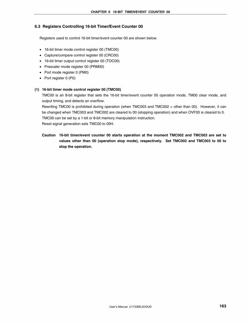
CHAPTER 6 16-BIT TIMER/EVENT COUNTER 00
User’s Manual U17336EJ5V0UD 163
6.3 Registers Controlling 16-bit Timer/Event Counter 00
Registers used to control 16-bit timer/event counter 00 are shown below.
• 16-bit timer mode control register 00 (TMC00)
• Capture/compare control register 00 (CRC00)
• 16-bit timer output control register 00 (TOC00)
• Prescaler mode register 00 (PRM00)
• Port mode register 0 (PM0)
• Port register 0 (P0)
(1) 16-bit timer mode control register 00 (TMC00)
TMC00 is an 8-bit register that sets the 16-bit timer/event counter 00 operation mode, TM00 clear mode, and
output timing, and detects an overflow.
Rewriting TMC00 is prohibited during operation (when TMC003 and TMC002 = other than 00). However, it can
be changed when TMC003 and TMC002 are cleared to 00 (stopping operation) and when OVF00 is cleared to 0.
TMC00 can be set by a 1-bit or 8-bit memory manipulation instruction.
Reset signal generation sets TMC00 to 00H.
Caution 16-bit timer/event counter 00 starts operation at the moment TMC002 and TMC003 are set to
values other than 00 (operation stop mode), respectively. Set TMC002 and TMC003 to 00 to
stop the operation.
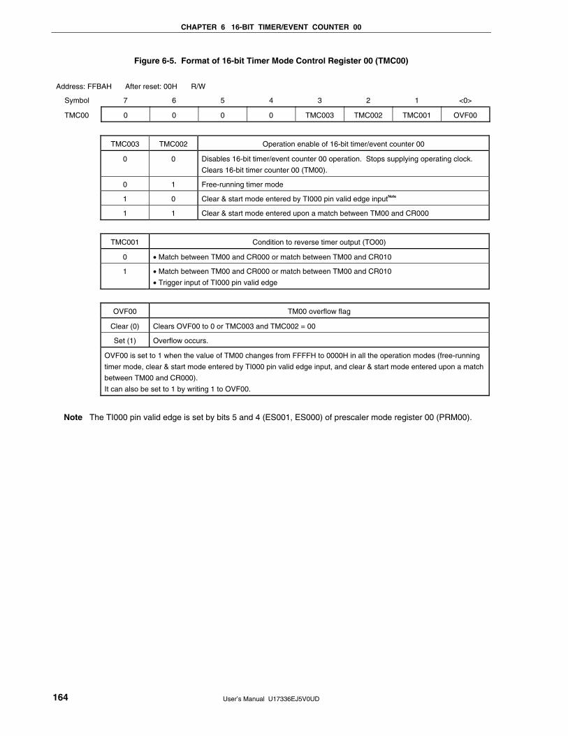
CHAPTER 6 16-BIT TIMER/EVENT COUNTER 00
User’s Manual U17336EJ5V0UD 164
Figure 6-5. Format of 16-bit Timer Mode Control Register 00 (TMC00)
Address: FFBAH After reset: 00H R/W
Symbol 7 6 5 4 3 2 1 <0>
TMC00 0 0 0 0 TMC003 TMC002 TMC001 OVF00
TMC003 TMC002 Operation enable of 16-bit timer/event counter 00
0 0 Disables 16-bit timer/event counter 00 operation. Stops supplying operating clock.
Clears 16-bit timer counter 00 (TM00).
0 1 Free-running timer mode
1 0 Clear & start mode entered by TI000 pin valid edge inputNote
1 1 Clear & start mode entered upon a match between TM00 and CR000
TMC001 Condition to reverse timer output (TO00)
0 • Match between TM00 and CR000 or match between TM00 and CR010
1 • Match between TM00 and CR000 or match between TM00 and CR010
• Trigger input of TI000 pin valid edge
OVF00 TM00 overflow flag
Clear (0) Clears OVF00 to 0 or TMC003 and TMC002 = 00
Set (1) Overflow occurs.
OVF00 is set to 1 when the value of TM00 changes from FFFFH to 0000H in all the operation modes (free-running
timer mode, clear & start mode entered by TI000 pin valid edge input, and clear & start mode entered upon a match
between TM00 and CR000).
It can also be set to 1 by writing 1 to OVF00.
Note The TI000 pin valid edge is set by bits 5 and 4 (ES001, ES000) of prescaler mode register 00 (PRM00).

CHAPTER 6 16-BIT TIMER/EVENT COUNTER 00
User’s Manual U17336EJ5V0UD 165
(2) Capture/compare control register 00 (CRC00)
CRC00 is the register that controls the operation of CR000 and CR010.
Changing the value of CRC00 is prohibited during operation (when TMC003 and TMC002 = other than 00).
CRC00 can be set by a 1-bit or 8-bit memory manipulation instruction.
Reset signal generation clears CRC00 to 00H.
Figure 6-6. Format of Capture/Compare Control Register 00 (CRC00)
Address: FFBCH After reset: 00H R/W
Symbol 7 6 5 4 3 2 1 0
CRC00 0 0 0 0 0 CRC002 CRC001 CRC000
CRC002 CR010 operating mode selection
0 Operates as compare register
1 Operates as capture register
CRC001 CR000 capture trigger selection
0 Captures on valid edge of TI010 pin
1 Captures on valid edge of TI000 pin by reverse phaseNote
The valid edge of the TI010 and TI000 pin is set by PRM00.
If ES001 and ES000 are set to 11 (both edges) when CRC001 is 1, the valid edge of the TI000 pin cannot
be detected.
CRC000 CR000 operating mode selection
0 Operates as compare register
1 Operates as capture register
If TMC003 and TMC002 are set to 11 (clear & start mode entered upon a match between TM00 and
CR000), be sure to set CRC000 to 0.
Note When the valid edge is detected from the TI010 pin, the capture operation is not performed but the
INTTM000 signal is generated as an external interrupt signal.
Caution To ensure that the capture operation is performed properly, the capture trigger requires a pulse
two cycles longer than the count clock selected by prescaler mode register 00 (PRM00).

CHAPTER 6 16-BIT TIMER/EVENT COUNTER 00
User’s Manual U17336EJ5V0UD 166
Figure 6-7. Example of CR010 Capture Operation (When Rising Edge Is Specified)
Count clock
TM00
TI000
Rising edge detection
CR010
INTTM010
N − 3 N − 2 N − 1 N N + 1
N
Valid edge
(3) 16-bit timer output control register 00 (TOC00)
TOC00 is an 8-bit register that controls TO00 output.
TOC00 can be rewritten while only OSPT00 is operating (when TMC003 and TMC002 = other than 00).
Rewriting the other bits is prohibited during operation.
However, TOC004 can be rewritten during timer operation as a means to rewrite CR010 (see 6.5.1 Rewriting
CR010 during TM00 operation).
TOC00 can be set by a 1-bit or 8-bit memory manipulation instruction.
Reset signal generation clears TOC00 to 00H.
Caution Be sure to set TOC00 using the following procedure.
<1> Set TOC004 and TOC001 to 1.
<2> Set only TOE00 to 1.
<3> Set either of LVS00 or LVR00 to 1.
<R>

CHAPTER 6 16-BIT TIMER/EVENT COUNTER 00
User’s Manual U17336EJ5V0UD 167
Figure 6-8. Format of 16-bit Timer Output Control Register 00 (TOC00)
Address: FFBDH After reset: 00H R/W
Symbol 7 <6> <5> 4 <3> <2> 1 <0>
TOC00 0 OSPT00 OSPE00 TOC004 LVS00 LVR00 TOC001 TOE00
OSPT00 One-shot pulse output trigger via software
0 −
1 One-shot pulse output
The value of this bit is always “0” when it is read. Do not set this bit to 1 in a mode other than the one-shot pulse output mode. If it is set to 1, TM00 is cleared and started.
OSPE00 One-shot pulse output operation control
0 Successive pulse output
1 One-shot pulse output
One-shot pulse output operates correctly in the free-running timer mode or clear & start mode entered by TI000 pin valid edge input. The one-shot pulse cannot be output in the clear & start mode entered upon a match between TM00 and CR000.
TOC004 TO00 output control on match between CR010 and TM00
0 Disables inversion operation
1 Enables inversion operation
The interrupt signal (INTTM010) is generated even when TOC004 = 0.
LVS00 LVR00 Setting of TO00 output status
0 0 No change
0 1 Initial value of TO00 output is low level (TO00 output is cleared to 0).
1 0 Initial value of TO00 output is high level (TO00 output is set to 1).
1 1 Setting prohibited
• LVS00 and LVR00 can be used to set the initial value of the TO00 output level. If the initial value does not have to be set, leave LVS00 and LVR00 as 00.
• Be sure to set LVS00 and LVR00 when TOE00 = 1. LVS00, LVR00, and TOE00 being simultaneously set to 1 is prohibited.
• LVS00 and LVR00 are trigger bits. By setting these bits to 1, the initial value of the TO00 output level can be set. Even if these bits are cleared to 0, TO00 output is not affected.
• The values of LVS00 and LVR00 are always 0 when they are read. • For how to set LVS00 and LVR00, see 6.5.2 Setting LVS00 and LVR00.
• The actual TO00/TI010/P01 pin output is determined depending on PM01 and P01, besides TO00 output.
TOC001 TO00 output control on match between CR000 and TM00
0 Disables inversion operation
1 Enables inversion operation
The interrupt signal (INTTM000) is generated even when TOC001 = 0.
TOE00 TO00 output control
0 Disables output (TO00 output fixed to low level)
1 Enables output
<R>

CHAPTER 6 16-BIT TIMER/EVENT COUNTER 00
User’s Manual U17336EJ5V0UD 168
(4) Prescaler mode register 00 (PRM00)
PRM00 is the register that sets the TM00 count clock and TI000 and TI010 pin input valid edges.
Rewriting PRM00 is prohibited during operation (when TMC003 and TMC002 = other than 00).
PRM00 can be set by a 1-bit or 8-bit memory manipulation instruction.
Reset signal generation clears PRM00 to 00H.
Cautions 1. Do not apply the following setting when setting the PRM001 and PRM000 bits to 11 (to
specify the valid edge of the TI000 pin as a count clock).
• Clear & start mode entered by the TI000 pin valid edge
• Setting the TI000 pin as a capture trigger
2. If the operation of the 16-bit timer/event counter 00 is enabled when the TI000 or TI010 pin is
at high level and when the valid edge of the TI000 or TI010 pin is specified to be the rising
edge or both edges, the high level of the TI000 or TI010 pin is detected as a rising edge.
Note this when the TI000 or TI010 pin is pulled up. However, the rising edge is not detected
when the timer operation has been once stopped and then is enabled again.
3. The valid edge of TI010 and timer output (TO00) cannot be used for the P01 pin at the same
time. Select either of the functions.

CHAPTER 6 16-BIT TIMER/EVENT COUNTER 00
User’s Manual U17336EJ5V0UD 169
Figure 6-9. Format of Prescaler Mode Register 00 (PRM00)
Address: FFBBH After reset: 00H R/W
Symbol 7 6 5 4 3 2 1 0
PRM00 ES101 ES100 ES001 ES000 0 0 PRM001 PRM000
ES101 ES100 TI010 pin valid edge selection
0 0 Falling edge
0 1 Rising edge
1 0 Setting prohibited
1 1 Both falling and rising edges
ES001 ES000 TI000 pin valid edge selection
0 0 Falling edge
0 1 Rising edge
1 0 Setting prohibited
1 1 Both falling and rising edges
Count clock selectionNote 1 PRM001 PRM000
fPRS = 2 MHz fPRS = 5 MHz fPRS = 10 MHz fPRS = 20 MHz
0 0 fPRSNote 2 2 MHz 5 MHz 10 MHz 20 MHz
0 1 fPRS/22 500 kHz 1.25 MHz 2.5 MHz 5 MHz
1 0 fPRS/28 7.81 kHz 19.53 kHz 39.06 kHz 78.12 kHz
1 1 TI000 valid edgeNote 3
Notes 1. If the peripheral hardware clock (fPRS) operates on the high-speed system clock (fXH) (XSEL = 1), the
fPRS operating frequency varies depending on the supply voltage.
• VDD = 4.0 to 5.5 V: fPRS ≤ 20 MHz
• VDD = 2.7 to 4.0 V: fPRS ≤ 10 MHz
• VDD = 1.8 to 2.7 V: fPRS ≤ 5 MHz (Standard and (A) grade products only)
2. If the peripheral hardware clock (fPRS) operates on the internal high-speed oscillation clock (fRH) (XSEL
= 0), when 1.8 V ≤ VDD < 2.7 V, the setting of PRM001 = PRM000 = 0 (count clock: fPRS) is prohibited.
3. The external clock from the TI000 pin requires a pulse longer than twice the cycle of the peripheral
hardware clock (fPRS).
Remark fPRS: Peripheral hardware clock frequency
<R>
<R>
<R>

CHAPTER 6 16-BIT TIMER/EVENT COUNTER 00
User’s Manual U17336EJ5V0UD 170
(5) Port mode register 0 (PM0)
This register sets port 0 input/output in 1-bit units.
When using the P01/TO00/TI010 pin for timer output, set PM01 and the output latches of P01 to 0.
When using the P00/TI000 and P01/TO00/TI010 pins for timer input, set PM00 and PM01 to 1. At this time, the
output latches of P00 and P01 may be 0 or 1.
PM0 can be set by a 1-bit or 8-bit memory manipulation instruction.
Reset signal generation sets PM0 to FFH.
Figure 6-10. Format of Port Mode Register 0 (PM0)
7
1
6
1
5
1
4
1
3
1
2
1
1
PM01
0
PM00
Symbol
PM0
Address: FF20H After reset: FFH R/W
PM0n
0
1
P0n pin I/O mode selection (n = 0, 1)
Output mode (output buffer on)
Input mode (output buffer off)

CHAPTER 6 16-BIT TIMER/EVENT COUNTER 00
User’s Manual U17336EJ5V0UD 171
6.4 Operation of 16-bit Timer/Event Counter 00
6.4.1 Interval timer operation
If bits 3 and 2 (TMC003 and TMC002) of the 16-bit timer mode control register (TMC00) are set to 11 (clear & start
mode entered upon a match between TM00 and CR000), the count operation is started in synchronization with the
count clock.
When the value of TM00 later matches the value of CR000, TM00 is cleared to 0000H and a match interrupt signal
(INTTM000) is generated. This INTTM000 signal enables TM00 to operate as an interval timer.
Remarks 1. For the setting of I/O pins, see 6.3 (5) Port mode register 0 (PM0).
2. For how to enable the INTTM000 interrupt, see CHAPTER 18 INTERRUPT FUNCTIONS.
Figure 6-11. Block Diagram of Interval Timer Operation
Figure 6-12. Basic Timing Example of Interval Timer Operation
TM00 register
0000H
Operable bits(TMC003, TMC002)
Compare register(CR000)
Compare match interrupt(INTTM000)
N
1100
N N N N
Interval(N + 1)
Interval(N + 1)
Interval(N + 1)
Interval(N + 1)
16-bit counter (TM00)
CR000 register
Operable bitsTMC003, TMC002
Count clock
Clear
Match signalINTTM000 signal

CHAPTER 6 16-BIT TIMER/EVENT COUNTER 00
User’s Manual U17336EJ5V0UD 172
Figure 6-13. Example of Register Settings for Interval Timer Operation
(a) 16-bit timer mode control register 00 (TMC00)
0 0 0 0 1 1 0 0
TMC003 TMC002 TMC001 OVF00
Clears and starts on match between TM00 and CR000.
(b) Capture/compare control register 00 (CRC00)
0 0 0 0 0 0 0 0
CRC002 CRC001 CRC000
CR000 used as compare register
(c) 16-bit timer output control register 00 (TOC00)
0 0 0 0 0
LVR00LVS00TOC004OSPE00OSPT00 TOC001 TOE00
0 0 0
(d) Prescaler mode register 00 (PRM00)
0 0 0 0 0
3 2 PRM001 PRM000ES101 ES100 ES001 ES000
Selects count clock
0 0/1 0/1
(e) 16-bit timer counter 00 (TM00)
By reading TM00, the count value can be read.
(f) 16-bit capture/compare register 000 (CR000)
If M is set to CR000, the interval time is as follows.
• Interval time = (M + 1) × Count clock cycle
Setting CR000 to 0000H is prohibited.
(g) 16-bit capture/compare register 010 (CR010)
Usually, CR010 is not used for the interval timer function. However, a compare match interrupt (INTTM010)
is generated when the set value of CR010 matches the value of TM00.
Therefore, mask the interrupt request by using the interrupt mask flag (TMMK010).

CHAPTER 6 16-BIT TIMER/EVENT COUNTER 00
User’s Manual U17336EJ5V0UD 173
Figure 6-14. Example of Software Processing for Interval Timer Function
TM00 register
0000H
Operable bits(TMC003, TMC002)
CR000 register
INTTM000 signal
N
1100
N N N
<1> <2>
TMC003, TMC002 bits = 11
TMC003, TMC002 bits = 00
Register initial settingPRM00 register,CRC00 register,CR000 register,
port setting
Initial setting of these registers is performed before setting the TMC003 and TMC002 bits to 11.
Starts count operation
The counter is initialized and counting is stopped by clearing the TMC003 and TMC002 bits to 00.
START
STOP
<1> Count operation start flow
<2> Count operation stop flow
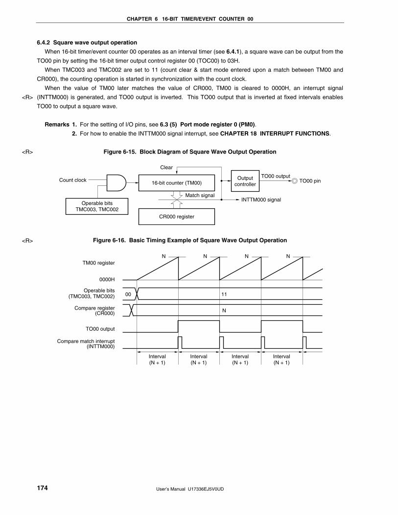
CHAPTER 6 16-BIT TIMER/EVENT COUNTER 00
User’s Manual U17336EJ5V0UD 174
6.4.2 Square wave output operation
When 16-bit timer/event counter 00 operates as an interval timer (see 6.4.1), a square wave can be output from the
TO00 pin by setting the 16-bit timer output control register 00 (TOC00) to 03H.
When TMC003 and TMC002 are set to 11 (count clear & start mode entered upon a match between TM00 and
CR000), the counting operation is started in synchronization with the count clock.
When the value of TM00 later matches the value of CR000, TM00 is cleared to 0000H, an interrupt signal
(INTTM000) is generated, and TO00 output is inverted. This TO00 output that is inverted at fixed intervals enables
TO00 to output a square wave.
Remarks 1. For the setting of I/O pins, see 6.3 (5) Port mode register 0 (PM0).
2. For how to enable the INTTM000 signal interrupt, see CHAPTER 18 INTERRUPT FUNCTIONS.
Figure 6-15. Block Diagram of Square Wave Output Operation
16-bit counter (TM00)
CR000 register
Operable bitsTMC003, TMC002
Count clock
Clear
Match signal
TO00 output
INTTM000 signal
Outputcontroller
TO00 pin
Figure 6-16. Basic Timing Example of Square Wave Output Operation
TM00 register
0000H
Operable bits(TMC003, TMC002)
Compare register(CR000)
TO00 output
Compare match interrupt(INTTM000)
N
1100
N N N N
Interval(N + 1)
Interval(N + 1)
Interval(N + 1)
Interval(N + 1)
<R>
<R>
<R>

CHAPTER 6 16-BIT TIMER/EVENT COUNTER 00
User’s Manual U17336EJ5V0UD 175
Figure 6-17. Example of Register Settings for Square Wave Output Operation
(a) 16-bit timer mode control register 00 (TMC00)
0 0 0 0 1 1 0 0
TMC003 TMC002 TMC001 OVF00
Clears and starts on match between TM00 and CR000.
(b) Capture/compare control register 00 (CRC00)
0 0 0 0 0 0 0 0
CRC002 CRC001 CRC000
CR000 used as compare register
(c) 16-bit timer output control register 00 (TOC00)
0 0 0 0 0/1
LVR00LVS00TOC004OSPE00OSPT00 TOC001 TOE00
Enables TO00 output.
Inverts TO00 output on match between TM00 and CR000.
0/1 1 1
Specifies initial value of TO00 output F/F
(d) Prescaler mode register 00 (PRM00)
0 0 0 0 0
3 2 PRM001 PRM000ES101 ES100 ES001 ES000
Selects count clock
0 0/1 0/1
(e) 16-bit timer counter 00 (TM00)
By reading TM00, the count value can be read.
(f) 16-bit capture/compare register 000 (CR000)
If M is set to CR000, the interval time is as follows.
• Square wave frequency = 1 / [2 × (M + 1) × Count clock cycle]
Setting CR000 to 0000H is prohibited.
(g) 16-bit capture/compare register 010 (CR010)
Usually, CR010 is not used for the square wave output function. However, a compare match interrupt
(INTTM010) is generated when the set value of CR010 matches the value of TM00.
Therefore, mask the interrupt request by using the interrupt mask flag (TMMK010).
<R>

CHAPTER 6 16-BIT TIMER/EVENT COUNTER 00
User’s Manual U17336EJ5V0UD 176
Figure 6-18. Example of Software Processing for Square Wave Output Function
TM00 register
0000H
Operable bits(TMC003, TMC002)
CR000 register
TO00 output
INTTM000 signal
TO00 output control bit(TOC001, TOE00)
TMC003, TMC002 bits = 11
TMC003, TMC002 bits = 00
Register initial settingPRM00 register,CRC00 register,
TOC00 registerNote,CR000 register,
port setting
Initial setting of these registers is performed before setting the TMC003 and TMC002 bits to 11.
Starts count operation
The counter is initialized and counting is stopped by clearing the TMC003 and TMC002 bits to 00.
START
STOP
<1> Count operation start flow
<2> Count operation stop flow
N
1100
N N N
<1> <2>
00
Note Care must be exercised when setting TOC00. For details, see 6.3 (3) 16-bit timer output control
register 00 (TOC00).
<R>
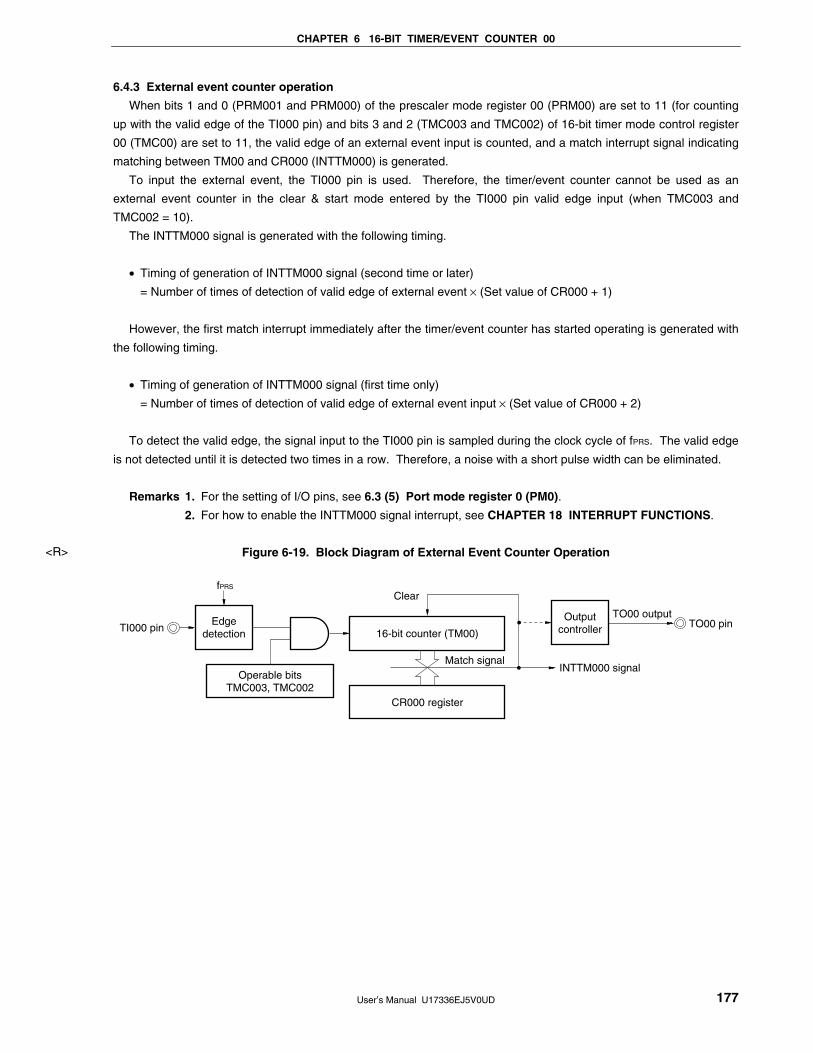
CHAPTER 6 16-BIT TIMER/EVENT COUNTER 00
User’s Manual U17336EJ5V0UD 177
6.4.3 External event counter operation
When bits 1 and 0 (PRM001 and PRM000) of the prescaler mode register 00 (PRM00) are set to 11 (for counting
up with the valid edge of the TI000 pin) and bits 3 and 2 (TMC003 and TMC002) of 16-bit timer mode control register
00 (TMC00) are set to 11, the valid edge of an external event input is counted, and a match interrupt signal indicating
matching between TM00 and CR000 (INTTM000) is generated.
To input the external event, the TI000 pin is used. Therefore, the timer/event counter cannot be used as an
external event counter in the clear & start mode entered by the TI000 pin valid edge input (when TMC003 and
TMC002 = 10).
The INTTM000 signal is generated with the following timing.
• Timing of generation of INTTM000 signal (second time or later)
= Number of times of detection of valid edge of external event × (Set value of CR000 + 1)
However, the first match interrupt immediately after the timer/event counter has started operating is generated with
the following timing.
• Timing of generation of INTTM000 signal (first time only)
= Number of times of detection of valid edge of external event input × (Set value of CR000 + 2)
To detect the valid edge, the signal input to the TI000 pin is sampled during the clock cycle of fPRS. The valid edge
is not detected until it is detected two times in a row. Therefore, a noise with a short pulse width can be eliminated.
Remarks 1. For the setting of I/O pins, see 6.3 (5) Port mode register 0 (PM0).
2. For how to enable the INTTM000 signal interrupt, see CHAPTER 18 INTERRUPT FUNCTIONS.
Figure 6-19. Block Diagram of External Event Counter Operation
16-bit counter (TM00)
CR000 register
Operable bitsTMC003, TMC002
Clear
Match signal
TO00 output
INTTM000 signal
fPRS
EdgedetectionTI000 pin
Outputcontroller TO00 pin
<R>

CHAPTER 6 16-BIT TIMER/EVENT COUNTER 00
User’s Manual U17336EJ5V0UD 178
Figure 6-20. Example of Register Settings in External Event Counter Mode (1/2)
(a) 16-bit timer mode control register 00 (TMC00)
0 0 0 0 1 1 0 0
TMC003 TMC002 TMC001 OVF00
Clears and starts on match between TM00 and CR000.
(b) Capture/compare control register 00 (CRC00)
0 0 0 0 0 0 0 0
CRC002 CRC001 CRC000
CR000 used as compare register
(c) 16-bit timer output control register 00 (TOC00)
0 0 0 0/1 0/1
LVR00LVS00TOC004OSPE00OSPT00 TOC001 TOE00
0/1 0/1 0/1
0: Disables TO00 output1: Enables TO00 output
00: Does not invert TO00 output on match between TM00 and CR000/CR010.
01: Inverts TO00 output on match between TM00 and CR000.
10: Inverts TO00 output on match between TM00 and CR010.
11: Inverts TO00 output on match between TM00 and CR000/CR010.
Specifies initial value of TO00 output F/F
(d) Prescaler mode register 00 (PRM00)
0 0 0/1 0/1 0
3 2 PRM001 PRM000ES101 ES100 ES001 ES000
Selects count clock(specifies valid edge of TI000).
00: Falling edge detection01: Rising edge detection10: Setting prohibited11: Both edges detection
0 1 1
(e) 16-bit timer counter 00 (TM00)
By reading TM00, the count value can be read.
(f) 16-bit capture/compare register 000 (CR000)
If M is set to CR000, the interrupt signal (INTTM000) is generated when the number of external events
reaches (M + 1).
Setting CR000 to 0000H is prohibited.

CHAPTER 6 16-BIT TIMER/EVENT COUNTER 00
User’s Manual U17336EJ5V0UD 179
Figure 6-20. Example of Register Settings in External Event Counter Mode (2/2)
(g) 16-bit capture/compare register 010 (CR010)
Usually, CR010 is not used in the external event counter mode. However, a compare match interrupt
(INTTM010) is generated when the set value of CR010 matches the value of TM00.
Therefore, mask the interrupt request by using the interrupt mask flag (TMMK010).
Figure 6-21. Example of Software Processing in External Event Counter Mode
TM00 register
0000H
Operable bits(TMC003, TMC002) 1100
N N N
TMC003, TMC002 bits = 11
TMC003, TMC002 bits = 00
Register initial settingPRM00 register,CRC00 register,
TOC00 registerNote,CR000 register,
port setting
START
STOP
<1> <2>
Compare match interrupt(INTTM000)
Compare register(CR000)
TO00 output control bits(TOC004, TOC001, TOE00)
TO00 output
N
00
Initial setting of these registers is performed before setting the TMC003 and TMC002 bits to 11.
Starts count operation
The counter is initialized and counting is stopped by clearing the TMC003 and TMC002 bits to 00.
<1> Count operation start flow
<2> Count operation stop flow
Note Care must be exercised when setting TOC00. For details, see 6.3 (3) 16-bit timer output control
register 00 (TOC00).
<R>
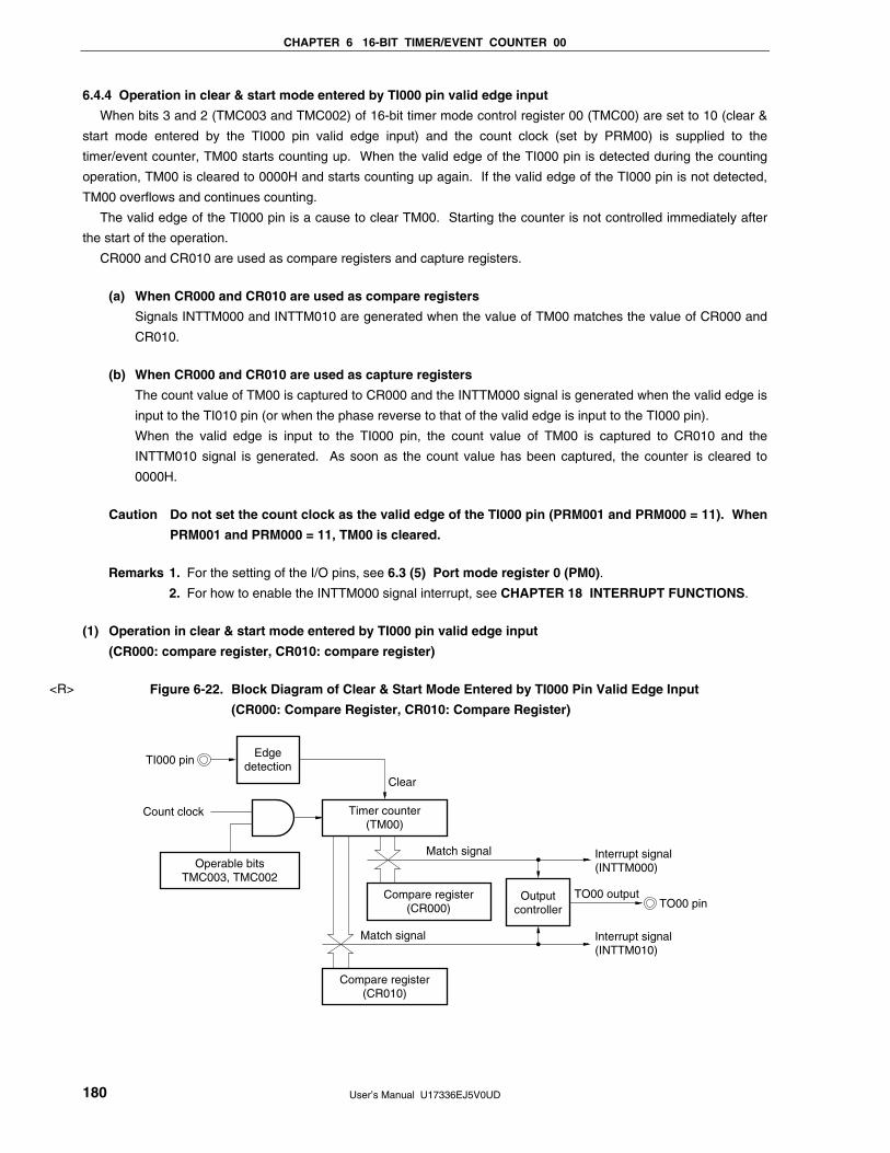
CHAPTER 6 16-BIT TIMER/EVENT COUNTER 00
User’s Manual U17336EJ5V0UD 180
6.4.4 Operation in clear & start mode entered by TI000 pin valid edge input
When bits 3 and 2 (TMC003 and TMC002) of 16-bit timer mode control register 00 (TMC00) are set to 10 (clear &
start mode entered by the TI000 pin valid edge input) and the count clock (set by PRM00) is supplied to the
timer/event counter, TM00 starts counting up. When the valid edge of the TI000 pin is detected during the counting
operation, TM00 is cleared to 0000H and starts counting up again. If the valid edge of the TI000 pin is not detected,
TM00 overflows and continues counting.
The valid edge of the TI000 pin is a cause to clear TM00. Starting the counter is not controlled immediately after
the start of the operation.
CR000 and CR010 are used as compare registers and capture registers.
(a) When CR000 and CR010 are used as compare registers
Signals INTTM000 and INTTM010 are generated when the value of TM00 matches the value of CR000 and
CR010.
(b) When CR000 and CR010 are used as capture registers
The count value of TM00 is captured to CR000 and the INTTM000 signal is generated when the valid edge is
input to the TI010 pin (or when the phase reverse to that of the valid edge is input to the TI000 pin).
When the valid edge is input to the TI000 pin, the count value of TM00 is captured to CR010 and the
INTTM010 signal is generated. As soon as the count value has been captured, the counter is cleared to
0000H.
Caution Do not set the count clock as the valid edge of the TI000 pin (PRM001 and PRM000 = 11). When
PRM001 and PRM000 = 11, TM00 is cleared.
Remarks 1. For the setting of the I/O pins, see 6.3 (5) Port mode register 0 (PM0).
2. For how to enable the INTTM000 signal interrupt, see CHAPTER 18 INTERRUPT FUNCTIONS.
(1) Operation in clear & start mode entered by TI000 pin valid edge input
(CR000: compare register, CR010: compare register)
Figure 6-22. Block Diagram of Clear & Start Mode Entered by TI000 Pin Valid Edge Input
(CR000: Compare Register, CR010: Compare Register)
Timer counter(TM00)
Clear
Outputcontroller
Edgedetection
Compare register(CR010)
Match signal
TO00 outputTO00 pin
Match signal Interrupt signal(INTTM000)
Interrupt signal(INTTM010)
TI000 pin
Compare register(CR000)
Operable bitsTMC003, TMC002
Count clock
<R>

CHAPTER 6 16-BIT TIMER/EVENT COUNTER 00
User’s Manual U17336EJ5V0UD 181
Figure 6-23. Timing Example of Clear & Start Mode Entered by TI000 Pin Valid Edge Input
(CR000: Compare Register, CR010: Compare Register)
(a) TOC00 = 13H, PRM00 = 10H, CRC00, = 00H, TMC00 = 08H
TM00 register
0000H
Operable bits(TMC003, TMC002)
Count clear input(TI000 pin input)
Compare register(CR000)
Compare match interrupt(INTTM000)
Compare register(CR010)
Compare match interrupt(INTTM010)
TO00 output
M
10
MN N N N
M M M
00
N
(b) TOC00 = 13H, PRM00 = 10H, CRC00, = 00H, TMC00 = 0AH
TM00 register
0000H
Operable bits(TMC003, TMC002)
Count clear input(TI000 pin input)
Compare register(CR000)
Compare match interrupt(INTTM000)
Compare register(CR010)
Compare match interrupt(INTTM010)
TO00 output
M
10
MN N N N
M M M
00
N
(a) and (b) differ as follows depending on the setting of bit 1 (TMC001) of 16-bit timer mode control register 01
(TMC00).
(a) The TO00 output level is inverted when TM00 matches a compare register.
(b) The TO00 output level is inverted when TM00 matches a compare register or when the valid edge of the
TI000 pin is detected.
<R>

CHAPTER 6 16-BIT TIMER/EVENT COUNTER 00
User’s Manual U17336EJ5V0UD 182
(2) Operation in clear & start mode entered by TI000 pin valid edge input
(CR000: compare register, CR010: capture register)
Figure 6-24. Block Diagram of Clear & Start Mode Entered by TI000 Pin Valid Edge Input
(CR000: Compare Register, CR010: Capture Register)
Timer counter(TM00)
Clear
Outputcontroller
Edgedetector
Capture register(CR010)
Capture signal
TO00 pin
Match signal
TO00 output
Interrupt signal(INTTM000)
Interrupt signal(INTTM010)
TI000 pin
Compare register(CR000)
Operable bitsTMC003, TMC002
Count clock
Figure 6-25. Timing Example of Clear & Start Mode Entered by TI000 Pin Valid Edge Input
(CR000: Compare Register, CR010: Capture Register) (1/2)
(a) TOC00 = 13H, PRM00 = 10H, CRC00 = 04H, TMC00 = 08H, CR000 = 0001H
TM00 register
0000H
Operable bits(TMC003, TMC002)
Capture & count clear input(TI000 pin input)
Compare register(CR000)
Compare match interrupt(INTTM000)
Capture register(CR010)
Capture interrupt(INTTM010)
TO00 output
0001H
10
QPNM
S
00
0000H M N S P Q
This is an application example where the TO00 output level is inverted when the count value has been captured
& cleared.
The count value is captured to CR010 and TM00 is cleared (to 0000H) when the valid edge of the TI000 pin is
detected. When the count value of TM00 is 0001H, a compare match interrupt signal (INTTM000) is generated,
and the TO00 output level is inverted.
<R>
<R>

CHAPTER 6 16-BIT TIMER/EVENT COUNTER 00
User’s Manual U17336EJ5V0UD 183
Figure 6-25. Timing Example of Clear & Start Mode Entered by TI000 Pin Valid Edge Input
(CR000: Compare Register, CR010: Capture Register) (2/2)
(b) TOC00 = 13H, PRM00 = 10H, CRC00 = 04H, TMC00 = 0AH, CR000 = 0003H
TM00 register
0000H
Operable bits(TMC003, TMC002)
Capture & count clear input(TI000 pin input)
Compare register(CR000)
Compare match interrupt(INTTM000)
Capture register(CR010)
Capture interrupt(INTTM010)
TO00 output
0003H
0003H
10
QPNM
S
00
0000H M
4 4 4 4
N S P Q
This is an application example where the width set to CR000 (4 clocks in this example) is to be output from the
TO00 pin when the count value has been captured & cleared.
The count value is captured to CR010, a capture interrupt signal (INTTM010) is generated, TM00 is cleared (to
0000H), and the TO00 output level is inverted when the valid edge of the TI000 pin is detected. When the count
value of TM00 is 0003H (four clocks have been counted), a compare match interrupt signal (INTTM000) is
generated and the TO00 output level is inverted.
<R>

CHAPTER 6 16-BIT TIMER/EVENT COUNTER 00
User’s Manual U17336EJ5V0UD 184
(3) Operation in clear & start mode entered by TI000 pin valid edge input
(CR000: capture register, CR010: compare register)
Figure 6-26. Block Diagram of Clear & Start Mode Entered by TI000 Pin Valid Edge Input
(CR000: Capture Register, CR010: Compare Register)
Timer counter(TM00)
Clear
Outputcontroller
Edgedetection
Capture register(CR000)
Capture signal
TO00 pin
Match signal
TO00 output
Interrupt signal(INTTM010)
Interrupt signal(INTTM000)
TI000 pin
Compare register(CR010)
Operable bitsTMC003, TMC002
Count clock
<R>
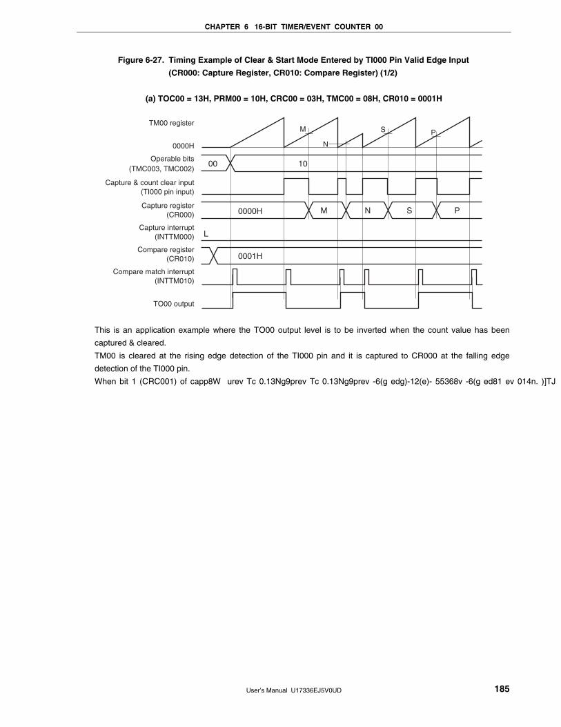
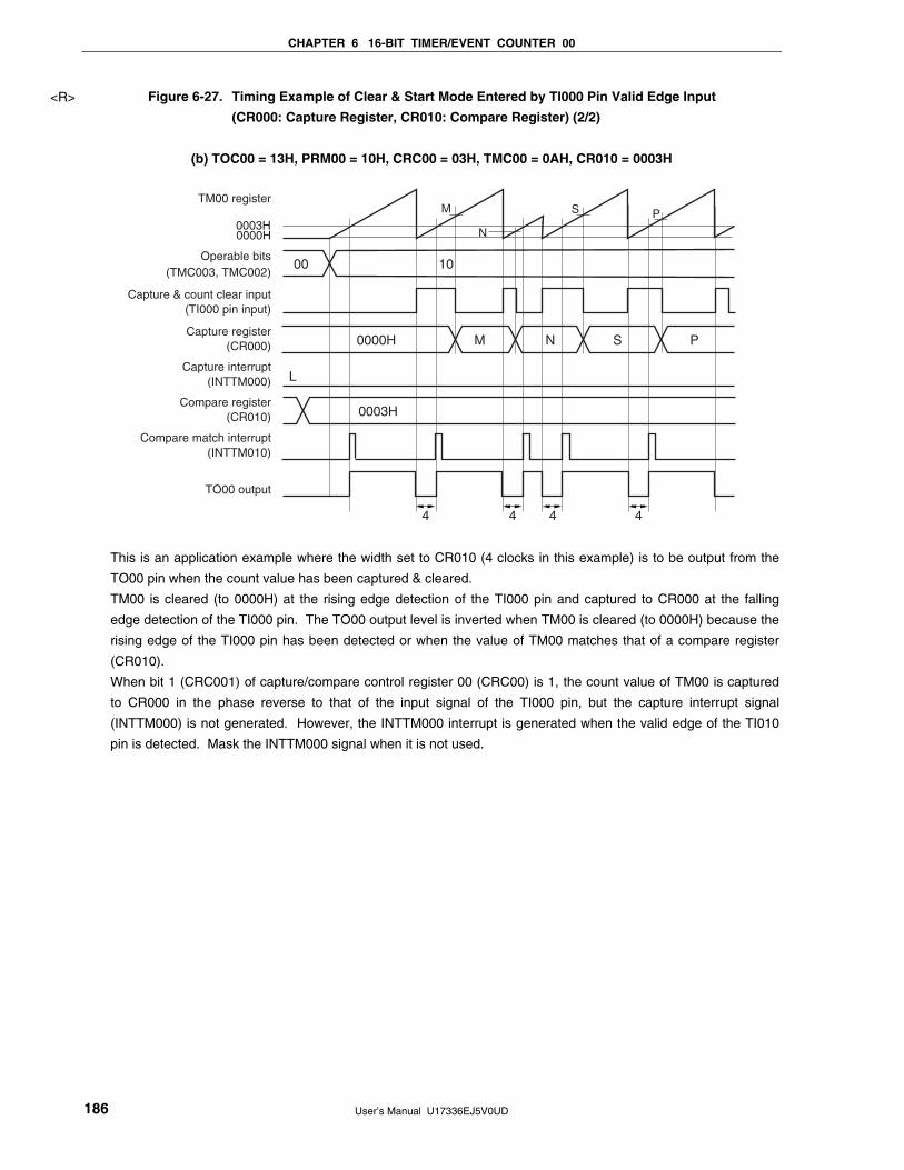
CHAPTER 6 16-BIT TIMER/EVENT COUNTER 00
User’s Manual U17336EJ5V0UD 186
Figure 6-27. Timing Example of Clear & Start Mode Entered by TI000 Pin Valid Edge Input
(CR000: Capture Register, CR010: Compare Register) (2/2)
(b) TOC00 = 13H, PRM00 = 10H, CRC00 = 03H, TMC00 = 0AH, CR010 = 0003H
TM00 register
0000H
Operable bits(TMC003, TMC002)
Capture & count clear input(TI000 pin input)
Capture register(CR000)
Capture interrupt(INTTM000)
Compare register(CR010)
Compare match interrupt(INTTM010)
TO00 output
0003H
0003H
10
P
N
M S
00
4 4 4 4
L
0000H M N S P
This is an application example where the width set to CR010 (4 clocks in this example) is to be output from the
TO00 pin when the count value has been captured & cleared.
TM00 is cleared (to 0000H) at the rising edge detection of the TI000 pin and captured to CR000 at the falling
edge detection of the TI000 pin. The TO00 output level is inverted when TM00 is cleared (to 0000H) because the
rising edge of the TI000 pin has been detected or when the value of TM00 matches that of a compare register
(CR010).
When bit 1 (CRC001) of capture/compare control register 00 (CRC00) is 1, the count value of TM00 is captured
to CR000 in the phase reverse to that of the input signal of the TI000 pin, but the capture interrupt signal
(INTTM000) is not generated. However, the INTTM000 interrupt is generated when the valid edge of the TI010
pin is detected. Mask the INTTM000 signal when it is not used.
<R>

CHAPTER 6 16-BIT TIMER/EVENT COUNTER 00
User’s Manual U17336EJ5V0UD 187
(4) Operation in clear & start mode entered by TI000 pin valid edge input
(CR000: capture register, CR010: capture register)
Figure 6-28. Block Diagram of Clear & Start Mode Entered by TI000 Pin Valid Edge Input
(CR000: Capture Register, CR010: Capture Register)
Timer counter(TM00)
Clear
TO00 outputOutputcontroller
Capture register(CR000)Capture
signal
Capture signal
TO00 pinNote
Interrupt signal(INTTM010)
Interrupt signal(INTTM000)
Capture register(CR010)
Operable bitsTMC003, TMC002
Count clock
EdgedetectionTI000 pin
EdgedetectionTI010 pinNote S
elec
tor
Note The timer output (TO00) cannot be used when detecting the valid edge of the TI010 pin is used.
Figure 6-29. Timing Example of Clear & Start Mode Entered by TI000 Pin Valid Edge Input
(CR000: Capture Register, CR010: Capture Register) (1/3)
(a) TOC00 = 13H, PRM00 = 30H, CRC00 = 05H, TMC00 = 0AH
TM00 register
0000H
Operable bits(TMC003, TMC002)
Capture & count clear input(TI000 pin input)
Capture register(CR000)
Capture interrupt(INTTM000)
Capture register(CR010)
Capture interrupt(INTTM010)
TO00 output
10
R S TO
L
MN
PQ
00
L
0000H
0000H L M N O P Q R S T
This is an application example where the count value is captured to CR010, TM00 is cleared, and TO00 output is
inverted when the rising or falling edge of the TI000 pin is detected.
When the edge of the TI010 pin is detected, an interrupt signal (INTTM000) is generated. Mask the INTTM000
signal when it is not used.
<R>
<R>

CHAPTER 6 16-BIT TIMER/EVENT COUNTER 00
User’s Manual U17336EJ5V0UD 188
Figure 6-29. Timing Example of Clear & Start Mode Entered by TI000 Pin Valid Edge Input
(CR000: Capture Register, CR010: Capture Register) (2/3)
(b) TOC00 = 13H, PRM00 = C0H, CRC00 = 05H, TMC00 = 0AH
TM00 register
0000H
Operable bits(TMC003, TMC002)
Capture trigger input(TI010 pin input)
Capture register(CR000)
Capture interrupt(INTTM000)
Capture & count clear input(TI000)
Capture register(CR010)
Capture interrupt(INTTM010)
10
R
S
TOL
MN
PQ
00
FFFFH
L
L
0000H
0000H
L M N O P Q R S T
This is a timing example where an edge is not input to the TI000 pin, in an application where the count value is
captured to CR000 when the rising or falling edge of the TI010 pin is detected.

CHAPTER 6 16-BIT TIMER/EVENT COUNTER 00
User’s Manual U17336EJ5V0UD 189
Figure 6-29. Timing Example of Clear & Start Mode Entered by TI000 Pin Valid Edge Input
(CR000: Capture Register, CR010: Capture Register) (3/3)
(c) TOC00 = 13H, PRM00 = 00H, CRC00 = 07H, TMC00 = 0AH
TM00 register
0000H
Operable bits(TMC003, TMC002)
Capture & count clear input(TI000 pin input)
Capture register(CR000)
Capture register(CR010)
Capture interrupt(INTTM010)
Capture input(TI010)
Capture interrupt(INTTM000)
0000H
10
P
OM
Q RT
S W
NL
00
L
L
L N RP T
0000H M O Q S W
This is an application example where the pulse width of the signal input to the TI000 pin is measured.
By setting CRC00, the count value can be captured to CR000 in the phase reverse to the falling edge of the
TI000 pin (i.e., rising edge) and to CR010 at the falling edge of the TI000 pin.
The high- and low-level widths of the input pulse can be calculated by the following expressions.
• High-level width = [CR010 value] – [CR000 value] × [Count clock cycle]
• Low-level width = [CR000 value] × [Count clock cycle]
If the reverse phase of the TI000 pin is selected as a trigger to capture the count value to CR000, the INTTM000
signal is not generated. Read the values of CR000 and CR010 to measure the pulse width immediately after the
INTTM010 signal is generated.
However, if the valid edge specified by bits 6 and 5 (ES101 and ES100) of prescaler mode register 00 (PRM00) is
input to the TI010 pin, the count value is not captured but the INTTM000 signal is generated. To measure the
pulse width of the TI000 pin, mask the INTTM000 signal when it is not used.

CHAPTER 6 16-BIT TIMER/EVENT COUNTER 00
User’s Manual U17336EJ5V0UD 190
Figure 6-30. Example of Register Settings in Clear & Start Mode Entered by TI000 Pin Valid Edge Input (1/2)
(a) 16-bit timer mode control register 00 (TMC00)
0 0 0 0 1 0 0/1 0
TMC003 TMC002 TMC001 OVF00
Clears and starts at valid edge input of TI000 pin.
0: Inverts TO00 output on matchbetween TM00 and CR000/CR010.
1: Inverts TO00 output on matchbetween TM00 and CR000/CR010and valid edge of TI000 pin.
(b) Capture/compare control register 00 (CRC00)
0 0 0 0 0 0/1 0/1 0/1
CRC002 CRC001 CRC000
0: CR000 used as compare register1: CR000 used as capture register
0: CR010 used as compare register1: CR010 used as capture register
0: TI010 pin is used as capture trigger of CR000.
1: Reverse phase of TI000 pin is used as capture trigger of CR000.
(c) 16-bit timer output control register 00 (TOC00)
0 0 0 0/1 0/1
LVR00LVS00TOC004OSPE00OSPT00 TOC001 TOE00
0: Disables TO00 outputNote
1: Enables TO00 output
00: Does not invert TO00 output on match between TM00 and CR000/CR010.
01: Inverts TO00 output on match between TM00 and CR000.
10: Inverts TO00 output on match between TM00 and CR010.
11: Inverts TO00 output on match between TM00 and CR000/CR010.
Specifies initial value of TO00 output F/F
0/1 0/1 0/1
Note The timer output (TO00) cannot be used when detecting the valid edge of the TI010 pin is used.

CHAPTER 6 16-BIT TIMER/EVENT COUNTER 00
User’s Manual U17336EJ5V0UD 191
Figure 6-30. Example of Register Settings in Clear & Start Mode Entered by TI000 Pin Valid Edge Input (2/2)
(d) Prescaler mode register 00 (PRM00)
0/1 0/1 0/1 0/1 0
3 2 PRM001 PRM000ES101 ES100 ES001 ES000
Count clock selection(setting TI000 valid edge is prohibited)
00: Falling edge detection01: Rising edge detection10: Setting prohibited11: Both edges detection
(setting prohibited when CRC001 = 1)
00: Falling edge detection01: Rising edge detection10: Setting prohibited11: Both edges detection
0 0/1 0/1
(e) 16-bit timer counter 00 (TM00)
By reading TM00, the count value can be read.
(f) 16-bit capture/compare register 000 (CR000)
When this register is used as a compare register and when its value matches the count value of TM00, an
interrupt signal (INTTM000) is generated. The count value of TM00 is not cleared.
To use this register as a capture register, select either the TI000 or TI010 pinNote input as a capture trigger.
When the valid edge of the capture trigger is detected, the count value of TM00 is stored in CR000.
Note The timer output (TO00) cannot be used when detection of the valid edge of the TI010 pin is used.
(g) 16-bit capture/compare register 010 (CR010)
When this register is used as a compare register and when its value matches the count value of TM00, an
interrupt signal (INTTM010) is generated. The count value of TM00 is not cleared.
When this register is used as a capture register, the TI000 pin input is used as a capture trigger. When the
valid edge of the capture trigger is detected, the count value of TM00 is stored in CR010.

CHAPTER 6 16-BIT TIMER/EVENT COUNTER 00
User’s Manual U17336EJ5V0UD 192
Figure 6-31. Example of Software Processing in Clear & Start Mode Entered by TI000 Pin Valid Edge Input
TM00 register
0000H
Operable bits(TMC003, TMC002)
Count clear input(TI000 pin input)
Compare register(CR000)
Compare match interrupt(INTTM000)
Compare register(CR010)
Compare match interrupt(INTTM010)
TO00 output
M
10
MN N N N
M M M
00
<1> <2> <2> <2> <3><2>
00
N
TMC003, TMC002 bits = 10
Edge input to TI000 pin
Register initial settingPRM00 register,CRC00 register,
TOC00 registerNote,CR000, CR010 registers,
TMC00.TMC001 bit,port setting
Initial setting of these registers is performed before setting the TMC003 and TMC002 bits to 10.
Starts count operation
When the valid edge is input to the TI000 pin, the value of the TM00 register is cleared.
START
<1> Count operation start flow
<2> TM00 register clear & start flow
TMC003, TMC002 bits = 00The counter is initialized and counting is stopped by clearing the TMC003 and TMC002 bits to 00.
STOP
<3> Count operation stop flow
Note Care must be exercised when setting TOC00. For details, see 6.3 (3) 16-bit timer output control register
00 (TOC00).
<R>

CHAPTER 6 16-BIT TIMER/EVENT COUNTER 00
User’s Manual U17336EJ5V0UD 193
6.4.5 Free-running timer operation
When bits 3 and 2 (TMC003 and TMC002) of 16-bit timer mode control register 00 (TMC00) are set to 01 (free-
running timer mode), 16-bit timer/event counter 00 continues counting up in synchronization with the count clock.
When it has counted up to FFFFH, the overflow flag (OVF00) is set to 1 at the next clock, and TM00 is cleared (to
0000H) and continues counting. Clear OVF00 to 0 by executing the CLR instruction via software.
The following three types of free-running timer operations are available.
• Both CR000 and CR010 are used as compare registers.
• One of CR000 or CR010 is used as a compare register and the other is used as a capture register.
• Both CR000 and CR010 are used as capture registers.
Remarks 1. For the setting of the I/O pins, see 6.3 (5) Port mode register 0 (PM0).
2. For how to enable the INTTM000 signal interrupt, see CHAPTER 18 INTERRUPT FUNCTIONS.
(1) Free-running timer mode operation
(CR000: compare register, CR010: compare register)
Figure 6-32. Block Diagram of Free-Running Timer Mode
(CR000: Compare Register, CR010: Compare Register)
Timer counter(TM00)
Outputcontroller
Compare register(CR010)
Match signal
TO00 pin
Match signal
TO00 output
Interrupt signal (INTTM000)
Interrupt signal (INTTM010)
Compare register(CR000)
Operable bitsTMC003, TMC002
Count clock
<R>

CHAPTER 6 16-BIT TIMER/EVENT COUNTER 00
User’s Manual U17336EJ5V0UD 194
Figure 6-33. Timing Example of Free-Running Timer Mode
(CR000: Compare Register, CR010: Compare Register)
• TOC00 = 13H, PRM00 = 00H, CRC00 = 00H, TMC00 = 04H
FFFFH
TM00 register
0000H
Operable bits(TMC003, TMC002)
Compare register(CR000)
Compare match interrupt(INTTM000)
Compare register(CR010)
Compare match interrupt(INTTM010)
TO00 output
OVF00 bit
01
MN
MN
MN
MN
00 00
N
0 write clear 0 write clear 0 write clear 0 write clear
M
This is an application example where two compare registers are used in the free-running timer mode.
The TO00 output level is inverted each time the count value of TM00 matches the set value of CR000 or CR010.
When the count value matches the register value, the INTTM000 or INTTM010 signal is generated.
(2) Free-running timer mode operation
(CR000: compare register, CR010: capture register)
Figure 6-34. Block Diagram of Free-Running Timer Mode
(CR000: Compare Register, CR010: Capture Register)
Timer counter(TM00)
Outputcontroller
Edgedetection
Capture register(CR010)Capture signal
TO00 pin
Match signal
TO00 output
Interrupt signal (INTTM000)
Interrupt signal (INTTM010)TI000 pin
Compare register(CR000)
Operable bitsTMC003, TMC002
Count clock
<R>
<R>

CHAPTER 6 16-BIT TIMER/EVENT COUNTER 00
User’s Manual U17336EJ5V0UD 195
Figure 6-35. Timing Example of Free-Running Timer Mode
(CR000: Compare Register, CR010: Capture Register)
• TOC00 = 13H, PRM00 = 10H, CRC00 = 04H, TMC00 = 04H
FFFFH
TM00 register
0000H
Operable bits(TMC003, TMC002)
Capture trigger input(TI000)
Compare register(CR000)
Compare match interrupt(INTTM000)
Capture register(CR010)
Capture interrupt(INTTM010)
TO00 output
Overflow flag(OVF00)
0 write clear 0 write clear 0 write clear 0 write clear
01
MN S P
Q
00
0000H
0000H
M N S P Q
This is an application example where a compare register and a capture register are used at the same time in the
free-running timer mode.
In this example, the INTTM000 signal is generated and the TO00 output level is inverted each time the count
value of TM00 matches the set value of CR000 (compare register). In addition, the INTTM010 signal is
generated and the count value of TM00 is captured to CR010 each time the valid edge of the TI000 pin is
detected.
<R>


CHAPTER 6 16-BIT TIMER/EVENT COUNTER 00
User’s Manual U17336EJ5V0UD 197
Figure 6-37. Timing Example of Free-Running Timer Mode
(CR000: Capture Register, CR010: Capture Register) (1/2)
(a) TOC00 = 13H, PRM00 = 50H, CRC00 = 05H, TMC00 = 04H
FFFFH
TM00 register
0000H
Operable bits(TMC003, TMC002)
Capture trigger input(TI000)
Capture register(CR010)
Capture interrupt(INTTM010)
Capture trigger input(TI010)
Capture register(CR000)
Capture interrupt(INTTM000)
Overflow flag(OVF00)
01
M
A B C D E
N S PQ
00
0 write clear 0 write clear 0 write clear 0 write clear
0000H A B C D E
0000H M N S P Q
This is an application example where the count values that have been captured at the valid edges of separate
capture trigger signals are stored in separate capture registers in the free-running timer mode.
The count value is captured to CR010 when the valid edge of the TI000 pin input is detected and to CR000 when
the valid edge of the TI010 pin input is detected.

CHAPTER 6 16-BIT TIMER/EVENT COUNTER 00
User’s Manual U17336EJ5V0UD 198
Figure 6-37. Timing Example of Free-Running Timer Mode
(CR000: Capture Register, CR010: Capture Register) (2/2)
(b) TOC00 = 13H, PRM00 = C0H, CRC00 = 05H, TMC00 = 04H
FFFFH
TM00 register
0000H
Operable bits(TMC003, TMC002)
Capture trigger input(TI010)
Capture register(CR000)
Capture interrupt(INTTM000)
Capture trigger input(TI000)
Capture register(CR010)
Capture interrupt(INTTM010)
01
L
M P S
NO R
QT
00
0000H
0000H
L M N O P Q R S T
L
L
This is an application example where both the edges of the TI010 pin are detected and the count value is
captured to CR000 in the free-running timer mode.
When both CR000 and CR010 are used as capture registers and when the valid edge of only the TI010 pin is to
be detected, the count value cannot be captured to CR010.

CHAPTER 6 16-BIT TIMER/EVENT COUNTER 00
User’s Manual U17336EJ5V0UD 199
Figure 6-38. Example of Register Settings in Free-Running Timer Mode (1/2)
(a) 16-bit timer mode control register 00 (TMC00)
0 0 0 0 0 1 0/1 0
TMC003 TMC002 TMC001 OVF00
Free-running timer mode
0: Inverts TO00 output on matchbetween TM00 and CR000/CR010.
1: Inverts TO00 output on matchbetween TM00 and CR000/CR010 and valid edge of TI000 pin.
(b) Capture/compare control register 00 (CRC00)
0 0 0 0 0 0/1 0/1 0/1
CRC002 CRC001 CRC000
0: CR000 used as compare register1: CR000 used as capture register
0: CR010 used as compare register1: CR010 used as capture register
0: TI010 pin is used as capture trigger of CR000.
1: Reverse phase of TI000 pin is used as capture trigger of CR000.
(c) 16-bit timer output control register 00 (TOC00)
0 0 0 0/1 0/1
LVR00LVS00TOC004OSPE00OSPT00 TOC001 TOE00
0: Disables TO00 output1: Enables TO00 output
00: Does not invert TO00 output on match between TM00 and CR000/CR010.
01: Inverts TO00 output on match between TM00 and CR000.
10: Inverts TO00 output on match between TM00 and CR010.
11: Inverts TO00 output on match between TM00 and CR000/CR010.
Specifies initial value of TO00 output F/F
0/1 0/1 0/1
<R>

CHAPTER 6 16-BIT TIMER/EVENT COUNTER 00
User’s Manual U17336EJ5V0UD 200
Figure 6-38. Example of Register Settings in Free-Running Timer Mode (2/2)
(d) Prescaler mode register 00 (PRM00)
0/1 0/1 0/1 0/1 0
3 2 PRM001 PRM000ES101 ES100 ES001 ES000
Count clock selection(setting TI000 valid edge is prohibited)
00: Falling edge detection01: Rising edge detection10: Setting prohibited11: Both edges detection
(setting prohibited when CRC001 = 1)
00: Falling edge detection01: Rising edge detection10: Setting prohibited11: Both edges detection
0 0/1 0/1
(e) 16-bit timer counter 00 (TM00)
By reading TM00, the count value can be read.
(f) 16-bit capture/compare register 000 (CR000)
When this register is used as a compare register and when its value matches the count value of TM00, an
interrupt signal (INTTM000) is generated. The count value of TM00 is not cleared.
To use this register as a capture register, select either the TI000 or TI010 pin input as a capture trigger.
When the valid edge of the capture trigger is detected, the count value of TM00 is stored in CR000.
(g) 16-bit capture/compare register 010 (CR010)
When this register is used as a compare register and when its value matches the count value of TM00, an
interrupt signal (INTTM010) is generated. The count value of TM00 is not cleared.
When this register is used as a capture register, the TI000 pin input is used as a capture trigger. When the
valid edge of the capture trigger is detected, the count value of TM00 is stored in CR010.

CHAPTER 6 16-BIT TIMER/EVENT COUNTER 00
User’s Manual U17336EJ5V0UD 201
Figure 6-39. Example of Software Processing in Free-Running Timer Mode
FFFFH
TM00 register
0000HOperable bits
(TMC003, TMC002)
Compare register(CR000)
Compare match interrupt(INTTM000)
Compare register(CR010)
Compare match interrupt(INTTM010)
Timer output control bits(TOE0, TOC004, TOC001)
TO00 output
M
01
N N N NMMM
00
<1> <2>
00
N
TMC003, TMC002 bits = 0, 1
Register initial settingPRM00 register,CRC00 register,
TOC00 registerNote,CR000/CR010 register,
TMC00.TMC001 bit,port setting
Initial setting of these registers is performed before setting the TMC003 and TMC002 bits to 01.
Starts count operation
START
<1> Count operation start flow
TMC003, TMC002 bits = 0, 0The counter is initialized and counting is stopped by clearing the TMC003 and TMC002 bits to 00.
STOP
<2> Count operation stop flow
Note Care must be exercised when setting TOC00. For details, see 6.3 (3) 16-bit timer output control
register 00 (TOC00).
<R>

CHAPTER 6 16-BIT TIMER/EVENT COUNTER 00
User’s Manual U17336EJ5V0UD 202
6.4.6 PPG output operation
A square wave having a pulse width set in advance by CR010 is output from the TO00 pin as a PPG
(Programmable Pulse Generator) signal during a cycle set by CR000 when bits 3 and 2 (TMC003 and TMC002) of 16-
bit timer mode control register 00 (TMC00) are set to 11 (clear & start upon a match between TM00 and CR000).
The pulse cycle and duty factor of the pulse generated as the PPG output are as follows.
• Pulse cycle = (Set value of CR000 + 1) × Count clock cycle
• Duty = (Set value of CR010 + 1) / (Set value of CR000 + 1)
Caution To change the duty factor (value of CR010) during operation, see 6.5.1 Rewriting CR010 during
TM00 operation.
Remarks 1. For the setting of I/O pins, see 6.3 (5) Port mode register 0 (PM0).
2. For how to enable the INTTM000 signal interrupt, see CHAPTER 18 INTERRUPT FUNCTIONS.
Figure 6-40. Block Diagram of PPG Output Operation
Timer counter(TM00)
Clear
Outputcontroller
Compare register(CR010)
Match signal
TO00 pin
Match signal
TO00 output
Interrupt signal (INTTM000)
Interrupt signal (INTTM010)
Compare register(CR000)
Operable bitsTMC003, TMC002
Count clock
<R>

CHAPTER 6 16-BIT TIMER/EVENT COUNTER 00
User’s Manual U17336EJ5V0UD 203
Figure 6-41. Example of Register Settings for PPG Output Operation
(a) 16-bit timer mode control register 00 (TMC00)
0 0 0 0 1 1 0 0
TMC003 TMC002 TMC001 OVF00
Clears and starts on match between TM00 and CR000.
(b) Capture/compare control register 00 (CRC00)
0 0 0 0 0 0 0 0
CRC002 CRC001 CRC000
CR000 used as compare register
CR010 used as compare register
(c) 16-bit timer output control register 00 (TOC00)
0 0 0 1 0/1
LVR00LVS00TOC004OSPE00OSPT00 TOC001 TOE00
Enables TO00 output
11: Inverts TO00 output on match between TM00 and CR000/CR010.
00: Disables one-shot pulse output
Specifies initial value of TO00 output F/F
0/1 1 1
(d) Prescaler mode register 00 (PRM00)
0 0 0 0 0
3 2 PRM001 PRM000ES101 ES100 ES001 ES000
Selects count clock
0 0/1 0/1
(e) 16-bit timer counter 00 (TM00)
By reading TM00, the count value can be read.
(f) 16-bit capture/compare register 000 (CR000)
An interrupt signal (INTTM000) is generated when the value of this register matches the count value of TM00.
The count value of TM00 is not cleared.
(g) 16-bit capture/compare register 010 (CR010)
An interrupt signal (INTTM010) is generated when the value of this register matches the count value of TM00.
The count value of TM00 is not cleared.
Caution Set values to CR000 and CR010 such that the condition 0000H ≤ CR010 < CR000 ≤ FFFFH is
satisfied.

CHAPTER 6 16-BIT TIMER/EVENT COUNTER 00
User’s Manual U17336EJ5V0UD 204
Figure 6-42. Example of Software Processing for PPG Output Operation
TM00 register
0000H
Operable bits(TMC003, TMC002)
Compare register(CR000)
Compare match interrupt(INTTM000)
Compare register(CR010)
Compare match interrupt(INTTM010)
Timer output control bits(TOE00, TOC004, TOC001)
TO00 output
M
11
M M M
NNN
00
<1>
N + 1
<2>
00
N
TMC003, TMC002 bits = 11
Register initial settingPRM00 register,CRC00 register,
TOC00 registerNote,CR000, CR010 registers,
port setting
Initial setting of these registers is performed before setting the TMC003 and TMC002 bits.
Starts count operation
START
<1> Count operation start flow
TMC003, TMC002 bits = 00The counter is initialized and counting is stopped by clearing the TMC003 and TMC002 bits to 00.
STOP
<2> Count operation stop flow
N + 1 N + 1M + 1M + 1M + 1
Note Care must be exercised when setting TOC00. For details, see 6.3 (3) 16-bit timer output control
register 00 (TOC00).
Remark PPG pulse cycle = (M + 1) × Count clock cycle
PPG duty = (N + 1) / (M + 1)
<R>
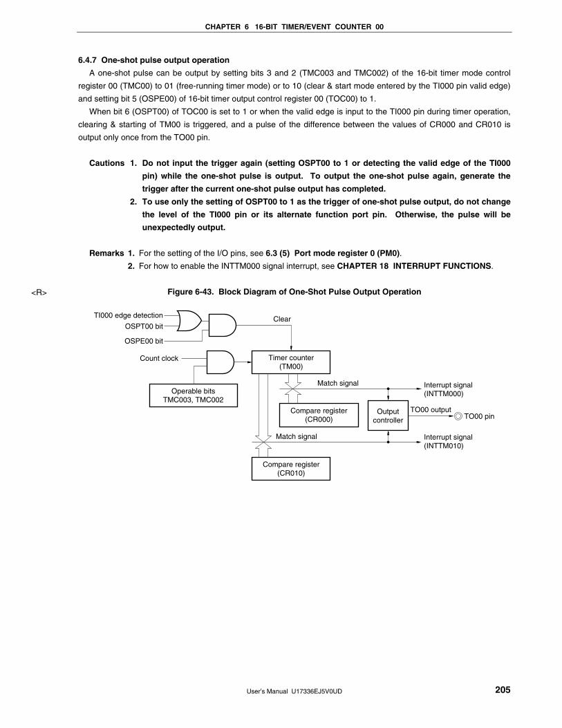
CHAPTER 6 16-BIT TIMER/EVENT COUNTER 00
User’s Manual U17336EJ5V0UD 205
6.4.7 One-shot pulse output operation
A one-shot pulse can be output by setting bits 3 and 2 (TMC003 and TMC002) of the 16-bit timer mode control
register 00 (TMC00) to 01 (free-running timer mode) or to 10 (clear & start mode entered by the TI000 pin valid edge)
and setting bit 5 (OSPE00) of 16-bit timer output control register 00 (TOC00) to 1.
When bit 6 (OSPT00) of TOC00 is set to 1 or when the valid edge is input to the TI000 pin during timer operation,
clearing & starting of TM00 is triggered, and a pulse of the difference between the values of CR000 and CR010 is
output only once from the TO00 pin.
Cautions 1. Do not input the trigger again (setting OSPT00 to 1 or detecting the valid edge of the TI000
pin) while the one-shot pulse is output. To output the one-shot pulse again, generate the
trigger after the current one-shot pulse output has completed.
2. To use only the setting of OSPT00 to 1 as the trigger of one-shot pulse output, do not change
the level of the TI000 pin or its alternate function port pin. Otherwise, the pulse will be
unexpectedly output.
Remarks 1. For the setting of the I/O pins, see 6.3 (5) Port mode register 0 (PM0).
2. For how to enable the INTTM000 signal interrupt, see CHAPTER 18 INTERRUPT FUNCTIONS.
Figure 6-43. Block Diagram of One-Shot Pulse Output Operation
Timer counter(TM00)
Outputcontroller
Compare register(CR010)
Match signal
TO00 pin
Match signal
TO00 output
Interrupt signal (INTTM000)
Interrupt signal (INTTM010)
Compare register(CR000)
Operable bitsTMC003, TMC002
Count clock
TI000 edge detection
OSPT00 bit
OSPE00 bit
Clear
<R>

CHAPTER 6 16-BIT TIMER/EVENT COUNTER 00
User’s Manual U17336EJ5V0UD 206
Figure 6-44. Example of Register Settings for One-Shot Pulse Output Operation (1/2)
(a) 16-bit timer mode control register 00 (TMC00)
0 0 0 0 0/1 0/1 0 0
TMC003 TMC002 TMC001 OVF00
01: Free running timer mode10: Clear and start mode by
valid edge of TI000 pin.
(b) Capture/compare control register 00 (CRC00)
0 0 0 0 0 0 0 0
CRC002 CRC001 CRC000
CR000 used as compare register
CR010 used as compare register
(c) 16-bit timer output control register 00 (TOC00)
0 0/1 1 1 0/1
LVR00LVS00TOC004OSPE00OSPT00 TOC001 TOE00
Enables TO00 output
Inverts TO00 output on match between TM00 and CR000/CR010.
Specifies initial value of TO00 output
Enables one-shot pulse output
Software trigger is generated by writing 1 to this bit (operation is not affected even if 0 is written to it).
0/1 1 1
(d) Prescaler mode register 00 (PRM00)
0 0 0 0 0
3 2 PRM001 PRM000ES101 ES100 ES001 ES000
Selects count clock
0 0/1 0/1
<R>

CHAPTER 6 16-BIT TIMER/EVENT COUNTER 00
User’s Manual U17336EJ5V0UD 207
Figure 6-44. Example of Register Settings for One-Shot Pulse Output Operation (2/2)
(e) 16-bit timer counter 00 (TM00)
By reading TM00, the count value can be read.
(f) 16-bit capture/compare register 000 (CR000)
This register is used as a compare register when a one-shot pulse is output. When the value of TM00
matches that of CR000, an interrupt signal (INTTM000) is generated and the TO00 output level is inverted.
(g) 16-bit capture/compare register 010 (CR010)
This register is used as a compare register when a one-shot pulse is output. When the value of TM00
matches that of CR010, an interrupt signal (INTTM010) is generated and the TO00 output level is inverted.
Caution Do not set the same value to CR000 and CR010.
<R>

CHAPTER 6 16-BIT TIMER/EVENT COUNTER 00
User’s Manual U17336EJ5V0UD 208
Figure 6-45. Example of Software Processing for One-Shot Pulse Output Operation (1/2)
FFFFH
TM00 register
0000H
Operable bits(TMC003, TMC002)
One-shot pulse enable bit(OSPE0)
One-shot pulse trigger bit(OSPT0)
One-shot pulse trigger input(TI000 pin)
Overflow plug(OVF00)
Compare register(CR000)
Compare match interrupt(INTTM000)
Compare register(CR010)
Compare match interrupt(INTTM010)
TO00 output
TO00 output control bits(TOE00, TOC004, TOC001)
N
M
N − M N − M
01 or 1000 00
NN NMM M
M + 1 M + 1
<1> <2> <2> <3>
TO00 output level is notinverted because no one-
shot trigger is input.
• Time from when the one-shot pulse trigger is input until the one-shot pulse is output
= (M + 1) × Count clock cycle
• One-shot pulse output active level width
= (N − M) × Count clock cycle
<R>

CHAPTER 6 16-BIT TIMER/EVENT COUNTER 00
User’s Manual U17336EJ5V0UD 209
Figure 6-45. Example of Software Processing for One-Shot Pulse Output Operation (2/2)
TMC003, TMC002 bits =01 or 10
Register initial settingPRM00 register,CRC00 register,
TOC00 registerNote,CR000, CR010 registers,
port setting
Initial setting of these registers is performed before setting the TMC003 and TMC002 bits.
Starts count operation
START
<1> Count operation start flow
<2> One-shot trigger input flow
TMC003, TMC002 bits = 00 The counter is initialized and counting is stopped by clearing the TMC003 and TMC002 bits to 00.
STOP
<3> Count operation stop flow
TOC00.OSPT00 bit = 1or edge input to TI000 pin
Write the same value to the bits other than the OSTP00 bit.
Note Care must be exercised when setting TOC00. For details, see 6.3 (3) 16-bit timer output control
register 00 (TOC00).

CHAPTER 6 16-BIT TIMER/EVENT COUNTER 00
User’s Manual U17336EJ5V0UD 210
6.4.8 Pulse width measurement operation
TM00 can be used to measure the pulse width of the signal input to the TI000 and TI010 pins.
Measurement can be accomplished by operating the 16-bit timer/event counter 00 in the free-running timer mode
or by restarting the timer in synchronization with the signal input to the TI000 pin.
When an interrupt is generated, read the value of the valid capture register and measure the pulse width. Check
bit 0 (OVF00) of 16-bit timer mode control register 00 (TMC00). If it is set (to 1), clear it to 0 by software.
Figure 6-46. Block Diagram of Pulse Width Measurement (Free-Running Timer Mode)
Timer counter(TM00)
Capture register(CR000)Capture
signal
Capture signal
Interrupt signal (INTTM010)
Interrupt signal (INTTM000)
Capture register(CR010)
Operable bitsTMC003, TMC002
Count clock
EdgedetectionTI000 pin
EdgedetectionTI010 pin S
elec
tor
Figure 6-47. Block Diagram of Pulse Width Measurement
(Clear & Start Mode Entered by TI000 Pin Valid Edge Input)
Timer counter(TM00)
Capture register(CR000)Capture
signal
Capture signal
Interrupt signal (INTTM010)
Interrupt signal (INTTM000)
Capture register(CR010)
Operable bitsTMC003, TMC002
Count clock
EdgedetectionTI000 pin
EdgedetectionTI010 pin
Clear
Sel
ecto
r

CHAPTER 6 16-BIT TIMER/EVENT COUNTER 00
User’s Manual U17336EJ5V0UD 211
A pulse width can be measured in the following three ways.
• Measuring the pulse width by using two input signals of the TI000 and TI010 pins (free-running timer mode)
• Measuring the pulse width by using one input signal of the TI000 pin (free-running timer mode)
• Measuring the pulse width by using one input signal of the TI000 pin (clear & start mode entered by the TI000 pin
valid edge input)
Remarks 1. For the setting of the I/O pins, see 6.3 (5) Port mode register 0 (PM0).
2. For how to enable the INTTM000 signal interrupt, see CHAPTER 18 INTERRUPT FUNCTIONS.
(1) Measuring the pulse width by using two input signals of the TI000 and TI010 pins (free-running timer
mode)
Set the free-running timer mode (TMC003 and TMC002 = 01). When the valid edge of the TI000 pin is detected,
the count value of TM00 is captured to CR010. When the valid edge of the TI010 pin is detected, the count value
of TM00 is captured to CR000. Specify detection of both the edges of the TI000 and TI010 pins.
By this measurement method, the previous count value is subtracted from the count value captured by the edge
of each input signal. Therefore, save the previously captured value to a separate register in advance.
If an overflow occurs, the value becomes negative if the previously captured value is simply subtracted from the
current captured value and, therefore, a borrow occurs (bit 0 (CY) of the program status word (PSW) is set to 1).
If this happens, ignore CY and take the calculated value as the pulse width. In addition, clear bit 0 (OVF00) of
16-bit timer mode control register 00 (TMC00) to 0.
Figure 6-48. Timing Example of Pulse Width Measurement (1)
• TMC00 = 04H, PRM00 = F0H, CRC00 = 05H
FFFFH
TM00 register
0000H
Operable bits(TMC003, TMC002)
Capture trigger input(TI000)
Capture register(CR010)
Capture interrupt(INTTM010)
Capture trigger input(TI010)
Capture register(CR000)
Capture interrupt(INTTM000)
Overflow flag(OVF00)
01
M
A B C D E
N S PQ
00
0 write clear 0 write clear 0 write clear 0 write clear
0000H A B C D E
0000H M N S P Q
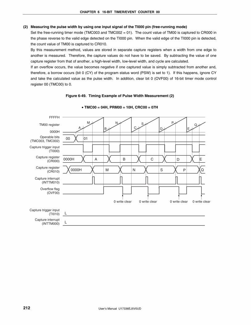
CHAPTER 6 16-BIT TIMER/EVENT COUNTER 00
User’s Manual U17336EJ5V0UD 212
(2) Measuring the pulse width by using one input signal of the TI000 pin (free-running mode)
Set the free-running timer mode (TMC003 and TMC002 = 01). The count value of TM00 is captured to CR000 in
the phase reverse to the valid edge detected on the TI000 pin. When the valid edge of the TI000 pin is detected,
the count value of TM00 is captured to CR010.
By this measurement method, values are stored in separate capture registers when a width from one edge to
another is measured. Therefore, the capture values do not have to be saved. By subtracting the value of one
capture register from that of another, a high-level width, low-level width, and cycle are calculated.
If an overflow occurs, the value becomes negative if one captured value is simply subtracted from another and,
therefore, a borrow occurs (bit 0 (CY) of the program status word (PSW) is set to 1). If this happens, ignore CY
and take the calculated value as the pulse width. In addition, clear bit 0 (OVF00) of 16-bit timer mode control
register 00 (TMC00) to 0.
Figure 6-49. Timing Example of Pulse Width Measurement (2)
• TMC00 = 04H, PRM00 = 10H, CRC00 = 07H
FFFFH
TM00 register
0000H
Operable bits(TMC003, TMC002)
Capture trigger input(TI000)
Capture register(CR000)
Capture register(CR010)
Capture interrupt(INTTM010)
Overflow flag(OVF00)
Capture trigger input(TI010)
Capture interrupt(INTTM000)
01
M
A B C D E
N S PQ
00
0 write clear 0 write clear 0 write clear 0 write clear
0000H
L
L
A B C D E
0000H M N S P Q

CHAPTER 6 16-BIT TIMER/EVENT COUNTER 00
User’s Manual U17336EJ5V0UD 213
(3) Measuring the pulse width by using one input signal of the TI000 pin (clear & start mode entered by the
TI000 pin valid edge input)
Set the clear & start mode entered by the TI000 pin valid edge (TMC003 and TMC002 = 10). The count value of
TM00 is captured to CR000 in the phase reverse to the valid edge of the TI000 pin, and the count value of TM00
is captured to CR010 and TM00 is cleared (0000H) when the valid edge of the TI000 pin is detected. Therefore,
a cycle is stored in CR010 if TM00 does not overflow.
If an overflow occurs, take the value that results from adding 10000H to the value stored in CR010 as a cycle.
Clear bit 0 (OVF00) of 16-bit timer mode control register 00 (TMC00) to 0.
Figure 6-50. Timing Example of Pulse Width Measurement (3)
• TMC00 = 08H, PRM00 = 10H, CRC00 = 07H
FFFFH
TM00 register
0000H
Operable bits(TMC003, TMC002)
Capture & count clear input(TI000)
Capture register(CR000)
Capture register(CR010)
Capture interrupt(INTTM010)
Overflow flag(OVF00)
Capture trigger input(TI010)
Capture interrupt(INTTM000)
10
<1>
<2> <3> <3> <3> <3><2> <2> <2>
<1> <1> <1>
M
A
BC D
N
S
P Q
00 00
0 write clear
0000H
L
L
A B C D
0000H M N S P Q
<1> Pulse cycle = (10000H × Number of times OVF00 bit is set to 1 + Captured value of CR010) ×
Count clock cycle
<2> High-level pulse width = (10000H × Number of times OVF00 bit is set to 1 + Captured value of CR000) ×
Count clock cycle
<3> Low-level pulse width = (Pulse cycle − High-level pulse width)

CHAPTER 6 16-BIT TIMER/EVENT COUNTER 00
User’s Manual U17336EJ5V0UD 214
Figure 6-51. Example of Register Settings for Pulse Width Measurement (1/2)
(a) 16-bit timer mode control register 00 (TMC00)
0 0 0 0 0/1 0/1 0 0
TMC003 TMC002 TMC001 OVF00
01: Free running timer mode10: Clear and start mode entered
by valid edge of TI000 pin.
(b) Capture/compare control register 00 (CRC00)
0 0 0 0 0 1 0/1 1
CRC002 CRC001 CRC000
1: CR000 used as capture register
1: CR010 used as capture register
0: TI010 pin is used as capture trigger of CR000.
1: Reverse phase of TI000 pin is used as capture trigger of CR000.
(c) 16-bit timer output control register 00 (TOC00)
0 0 0 0 0
LVR00LVS00TOC004OSPE00OSPT00 TOC001 TOE00
0 0 0
(d) Prescaler mode register 00 (PRM00)
0/1 0/1 0/1 0/1 0
3 2 PRM001 PRM000ES101 ES100 ES001 ES000
Selects count clock(setting valid edge of TI000 is prohibited)
00: Falling edge detection01: Rising edge detection10: Setting prohibited11: Both edges detection
(setting when CRC001 = 1 is prohibited)
00: Falling edge detection01: Rising edge detection10: Setting prohibited11: Both edges detection
0 0/1 0/1

CHAPTER 6 16-BIT TIMER/EVENT COUNTER 00
User’s Manual U17336EJ5V0UD 215
Figure 6-51. Example of Register Settings for Pulse Width Measurement (2/2)
(e) 16-bit timer counter 00 (TM00)
By reading TM00, the count value can be read.
(f) 16-bit capture/compare register 000 (CR000)
This register is used as a capture register. Either the TI000 or TI010 pin is selected as a capture trigger.
When a specified edge of the capture trigger is detected, the count value of TM00 is stored in CR000.
(g) 16-bit capture/compare register 010 (CR010)
This register is used as a capture register. The signal input to the TI000 pin is used as a capture trigger.
When the capture trigger is detected, the count value of TM00 is stored in CR010.
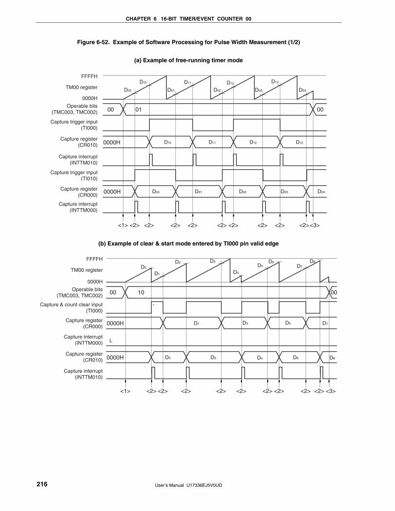
CHAPTER 6 16-BIT TIMER/EVENT COUNTER 00
User’s Manual U17336EJ5V0UD 216
Figure 6-52. Example of Software Processing for Pulse Width Measurement (1/2)
(a) Example of free-running timer mode
FFFFH
TM00 register
0000H
Operable bits(TMC003, TMC002)
Capture trigger input(TI000)
Capture register(CR010)
Capture interrupt(INTTM010)
Capture trigger input(TI010)
Capture register(CR000)
Capture interrupt(INTTM000)
01
D00
D00
D01
D01
D02
D02
D03
D03
D04
D04
D10
D10
D11
D11
D12
D12
D13
D13
00 00
0000H
0000H
<1> <2> <2> <2> <2> <2> <2> <2> <2> <2><3>
(b) Example of clear & start mode entered by TI000 pin valid edge
FFFFH
TM00 register
0000H
Operable bits(TMC003, TMC002)
Capture & count clear input(TI000)
Capture register(CR000)
Capture interrupt(INTTM000)
Capture register(CR010)
Capture interrupt(INTTM010)
10
D0
L
D0
D1
D1
D2
D2
D3
D3
D4
D4
D5
D5
D6
D6
D7
D7
D8
D8
00 00
0000H
0000H
<1> <2> <2> <2> <2> <2> <2> <2> <2> <3><2>

CHAPTER 6 16-BIT TIMER/EVENT COUNTER 00
User’s Manual U17336EJ5V0UD 217
Figure 6-52. Example of Software Processing for Pulse Width Measurement (2/2)
<2> Capture trigger input flow
Edge detection of TI000, TI010 pins
Calculated pulse widthfrom capture value
Stores count value to CR000, CR010 registers
Generates capture interruptNote
TMC003, TMC002 bits =01 or 10
Register initial settingPRM00 register,CRC00 register,
port setting
Initial setting of these registers is performed before setting the TMC003 and TMC002 bits.
Starts count operation
START
<1> Count operation start flow
TMC003, TMC002 bits = 00 The counter is initialized and counting is stopped by clearing the TMC003 and TMC002 bits to 00.
STOP
<3> Count operation stop flow
Note The capture interrupt signal (INTTM000) is not generated when the reverse-phase edge of the TI000 pin
input is selected to the valid edge of CR000.

CHAPTER 6 16-BIT TIMER/EVENT COUNTER 00
User’s Manual U17336EJ5V0UD 218
6.5 Special Use of TM00
6.5.1 Rewriting CR010 during TM00 operation
In principle, rewriting CR000 and CR010 of the 78K0/KC2 when they are used as compare registers is prohibited
while TM00 is operating (TMC003 and TMC002 = other than 00).
However, the value of CR010 can be changed, even while TM00 is operating, using the following procedure if
CR010 is used for PPG output and the duty factor is changed. (When changing the value of CR010 to a smaller value
than the current one, rewrite it immediately after its value matches the value of TM00. When changing the value of
CR010 to a larger value than the current one, rewrite it immediately after the values of CR000 and TM00 match. If the
value of CR010 is rewritten immediately before a match between CR010 and TM00, or between CR000 and TM00, an
unexpected operation may be performed.).
Procedure for changing value of CR010
<1> Disable interrupt INTTM010 (TMMK010 = 1).
<2> Disable reversal of the timer output when the value of TM00 matches that of CR010 (TOC004 = 0).
<3> Change the value of CR010.
<4> Wait for one cycle of the count clock of TM00.
<5> Enable reversal of the timer output when the value of TM00 matches that of CR010 (TOC004 = 1).
<6> Clear the interrupt flag of INTTM010 (TMIF010 = 0) to 0.
<7> Enable interrupt INTTM010 (TMMK010 = 0).
Remark For TMIF010 and TMMK010, see CHAPTER 18 INTERRUPT FUNCTIONS.
6.5.2 Setting LVS00 and LVR00
(1) Usage of LVS00 and LVR00
LVS00 and LVR00 are used to set the default value of TO00 output and to invert the timer output without enabling
the timer operation (TMC003 and TMC002 = 00). Clear LVS00 and LVR00 to 00 (default value: low-level output)
when software control is unnecessary.
LVS00 LVR00 Timer Output Status
0 0 Not changed (low-level output)
0 1 Cleared (low-level output)
1 0 Set (high-level output)
1 1 Setting prohibited
<R>
<R>
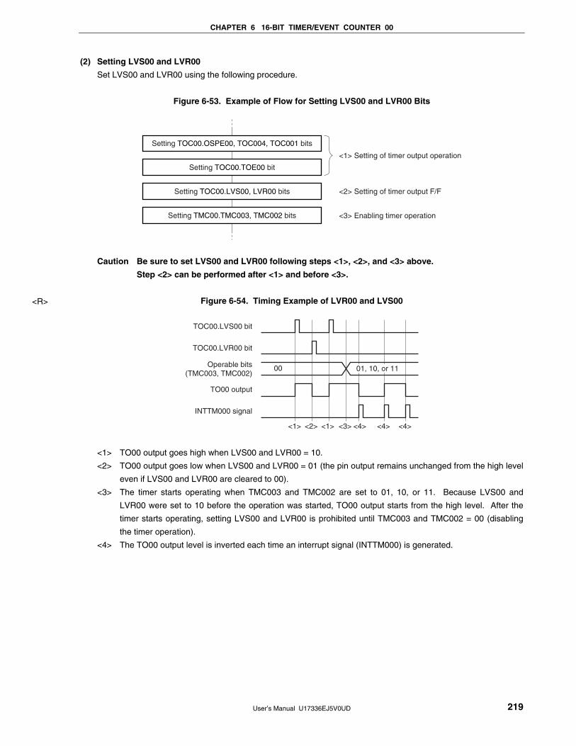
CHAPTER 6 16-BIT TIMER/EVENT COUNTER 00
User’s Manual U17336EJ5V0UD 219
(2) Setting LVS00 and LVR00
Set LVS00 and LVR00 using the following procedure.
Figure 6-53. Example of Flow for Setting LVS00 and LVR00 Bits
Setting TOC00.OSPE00, TOC004, TOC001 bits
Setting TOC00.TOE00 bit
Setting TOC00.LVS00, LVR00 bits
Setting TMC00.TMC003, TMC002 bits <3> Enabling timer operation
<2> Setting of timer output F/F
<1> Setting of timer output operation
Caution Be sure to set LVS00 and LVR00 following steps <1>, <2>, and <3> above.
Step <2> can be performed after <1> and before <3>.
Figure 6-54. Timing Example of LVR00 and LVS00
TOC00.LVS00 bit
TOC00.LVR00 bit
Operable bits(TMC003, TMC002)
TO00 output
INTTM000 signal
<1>
00
<2> <1> <3> <4> <4> <4>
01, 10, or 11
<1> TO00 output goes high when LVS00 and LVR00 = 10.
<2> TO00 output goes low when LVS00 and LVR00 = 01 (the pin output remains unchanged from the high level
even if LVS00 and LVR00 are cleared to 00).
<3> The timer starts operating when TMC003 and TMC002 are set to 01, 10, or 11. Because LVS00 and
LVR00 were set to 10 before the operation was started, TO00 output starts from the high level. After the
timer starts operating, setting LVS00 and LVR00 is prohibited until TMC003 and TMC002 = 00 (disabling
the timer operation).
<4> The TO00 output level is inverted each time an interrupt signal (INTTM000) is generated.
<R>

CHAPTER 6 16-BIT TIMER/EVENT COUNTER 00
User’s Manual U17336EJ5V0UD 220
6.6 Cautions for 16-bit Timer/Event Counter 00
(1) Restrictions for each channel of 16-bit timer/event counter 00
Table 6-3 shows the restrictions for each channel.
Table 6-3. Restrictions for Each Channel of 16-bit Timer/Event Counter 00
Operation Restriction
As interval timer
As square wave output
As external event counter
−
As clear & start mode entered by
TI000 pin valid edge input
Using timer output (TO00) is prohibited when detection of the valid edge of the TI010 pin is
used. (TOC00 = 00H)
As free-running timer −
As PPG output 0000H ≤ CR010 < CR000 ≤ FFFFH
As one-shot pulse output Setting the same value to CR000 and CR010 is prohibited.
As pulse width measurement Using timer output (TO00) is prohibited (TOC00 = 00H)
(2) Timer start errors
An error of up to one clock may occur in the time required for a match signal to be generated after timer start.
This is because counting TM00 is started asynchronously to the count pulse.
Figure 6-55. Start Timing of TM00 Count
0000H
Timer start
0001H 0002H 0003H 0004H
Count pulse
TM00 count value
(3) Setting of CR000 and CR010 (clear & start mode entered upon a match between TM00 and CR000)
Set a value other than 0000H to CR000 and CR010 (TM00 cannot count one pulse when it is used as an external
event counter).

CHAPTER 6 16-BIT TIMER/EVENT COUNTER 00
User’s Manual U17336EJ5V0UD 221
(4) Timing of holding data by capture register
(a) When the valid edge is input to the TI000/TI010 pin and the reverse phase of the TI000 pin is detected while
CR000/CR010 is read, CR010 performs a capture operation but the read value of CR000/CR010 is not
guaranteed. At this time, an interrupt signal (INTTM000/INTTM010) is generated when the valid edge of the
TI000/TI010 pin is detected (the interrupt signal is not generated when the reverse-phase edge of the TI000
pin is detected).
When the count value is captured because the valid edge of the TI000/TI010 pin was detected, read the
value of CR000/CR010 after INTTM000/INTTM010 is generated.
Figure 6-56. Timing of Holding Data by Capture Register
N N + 1 N + 2
X N + 1
M M + 1 M + 2
Count pulse
TM00 count value
Edge input
INTTM010
Value captured to CR010
Capture read signal
Capture operation is performed but read value is not guaranteed.
Capture operation
(b) The values of CR000 and CR010 are not guaranteed after 16-bit timer/event counter 00 stops.
(5) Setting valid edge
Set the valid edge of the TI000 pin while the timer operation is stopped (TMC003 and TMC002 = 00). Set the
valid edge by using ES000 and ES001.
(6) Re-triggering one-shot pulse
Make sure that the trigger is not generated while an active level is being output in the one-shot pulse output mode.
Be sure to input the next trigger after the current active level is output.

CHAPTER 6 16-BIT TIMER/EVENT COUNTER 00
User’s Manual U17336EJ5V0UD 222
(7) Operation of OVF00 flag
(a) Setting OVF00 flag (1)
The OVF00 flag is set to 1 in the following case, as well as when TM00 overflows.
Select the clear & start mode entered upon a match between TM00 and CR000.
↓
Set CR000 to FFFFH.
↓
When TM00 matches CR000 and TM00 is cleared from FFFFH to 0000H
Figure 6-57. Operation Timing of OVF00 Flag
FFFEH
FFFFH
FFFFH 0000H 0001H
Count pulse
TM00
INTTM000
OVF00
CR000
(b) Clearing OVF00 flag
Even if the OVF00 flag is cleared to 0 after TM00 overflows and before the next count clock is counted
(before the value of TM00 becomes 0001H), it is set to 1 again and clearing is invalid.
(8) One-shot pulse output
One-shot pulse output operates correctly in the free-running timer mode or the clear & start mode entered by the
TI000 pin valid edge. The one-shot pulse cannot be output in the clear & start mode entered upon a match
between TM00 and CR000.

CHAPTER 6 16-BIT TIMER/EVENT COUNTER 00
User’s Manual U17336EJ5V0UD 223
(9) Capture operation
(a) When valid edge of TI000 is specified as count clock
When the valid edge of TI000 is specified as the count clock, the capture register for which TI000 is specified
as a trigger does not operate correctly.
(b) Pulse width to accurately capture value by signals input to TI010 and TI000 pins
To accurately capture the count value, the pulse input to the TI000 and TI010 pins as a capture trigger must
be wider than two count clocks selected by PRM00 (see Figure 6-7).
(c) Generation of interrupt signal
The capture operation is performed at the falling edge of the count clock but the interrupt signals (INTTM000
and INTTM010) are generated at the rising edge of the next count clock (see Figure 6-7).
(d) Note when CRC001 (bit 1 of capture/compare control register 00 (CRC00)) is set to 1
When the count value of the TM00 register is captured to the CR000 register in the phase reverse to the
signal input to the TI000 pin, the interrupt signal (INTTM000) is not generated after the count value is
captured. If the valid edge is detected on the TI010 pin during this operation, the capture operation is not
performed but the INTTM000 signal is generated as an external interrupt signal. Mask the INTTM000 signal
when the external interrupt is not used.
(10) Edge detection
(a) Specifying valid edge after reset
If the operation of the 16-bit timer/event counter 00 is enabled after reset and while the TI000 or TI010 pin is
at high level and when the rising edge or both the edges are specified as the valid edge of the TI000 or TI010
pin, then the high level of the TI000 or TI010 pin is detected as the rising edge. Note this when the TI000 or
TI010 pin is pulled up. However, the rising edge is not detected when the operation is once stopped and
then enabled again.
(b) Sampling clock for eliminating noise
The sampling clock for eliminating noise differs depending on whether the valid edge of TI000 is used as the
count clock or capture trigger. In the former case, the sampling clock is fixed to fPRS. In the latter, the count
clock selected by PRM00 is used for sampling.
When the signal input to the TI000 pin is sampled and the valid level is detected two times in a row, the valid
edge is detected. Therefore, noise having a short pulse width can be eliminated (see Figure 6-7).
(11) Timer operation
The signal input to the TI000/TI010 pin is not acknowledged while the timer is stopped, regardless of the
operation mode of the CPU.
Remark fPRS: Peripheral hardware clock frequency

User’s Manual U17336EJ5V0UD 224
CHAPTER 7 8-BIT TIMER/EVENT COUNTERS 50 AND 51
7.1 Functions of 8-bit Timer/Event Counters 50 and 51
8-bit timer/event counters 50 and 51 have the following functions.
• Interval timer
• External event counter
• Square-wave output
• PWM output
7.2 Configuration of 8-bit Timer/Event Counters 50 and 51
8-bit timer/event counters 50 and 51 include the following hardware.
Table 7-1. Configuration of 8-bit Timer/Event Counters 50 and 51
Item Configuration
Timer register 8-bit timer counter 5n (TM5n)
Register 8-bit timer compare register 5n (CR5n)
Timer input TI5n
Timer output TO5n
Control registers Timer clock selection register 5n (TCL5n)
8-bit timer mode control register 5n (TMC5n)
Port mode register 1 (PM1) or port mode register 3 (PM3)
Port register 1 (P1) or port register 3 (P3)
Figures 7-1 and 7-2 show the block diagrams of 8-bit timer/event counters 50 and 51.

CHAPTER 7 8-BIT TIMER/EVENT COUNTERS 50 AND 51
User’s Manual U17336EJ5V0UD 225
Figure 7-1. Block Diagram of 8-bit Timer/Event Counter 50
Internal bus
8-bit timer compareregister 50 (CR50)
TI50/TO50/P17
fPRS/213
fPRS
fPRS/2
Match
Mas
k ci
rcui
t
OVF
3
Clear
TCL502 TCL501 TCL500
Timer clock selectionregister 50 (TCL50)
Internal bus
TCE50 TMC506 LVS50 LVR50 TMC501 TOE50
Invertlevel
8-bit timer mode control register 50 (TMC50)
S
R
SQ
R
INV
SelectorTo TMH0To UART0To UART6
INTTM50
TO50output
TO50/TI50/P17
Note 1
Note 2
Sel
ecto
r
8-bit timercounter 50 (TM50)S
elec
tor
Output latch(P17)
PM17
fPRS/22
fPRS/28fPRS/26
Figure 7-2. Block Diagram of 8-bit Timer/Event Counter 51
Internal bus
8-bit timer compareregister 51 (CR51)
TI51/TO51/P33/INTP4
fPRS/212
fPRS
fPRS/2
Match
Mas
k ci
rcui
t
OVF
3
Clear
TCL512 TCL511 TCL510
Timer clock selectionregister 51 (TCL51)
Internal bus
TCE51 TMC516 LVS51 LVR51 TMC511 TOE51
Invertlevel
8-bit timer mode control register 51 (TMC51)
S
R
SQ
R
INV
Selector INTTM51
TO51 output
TO51/TI51/P33/INTP4
Note 1
Note 2
Sel
ecto
r
8-bit timercounter 51 (TM51)S
elec
tor
Output latch(P33)
PM33
fPRS/26fPRS/24
fPRS/28
Notes 1. Timer output F/F
2. PWM output F/F
<R>
<R>
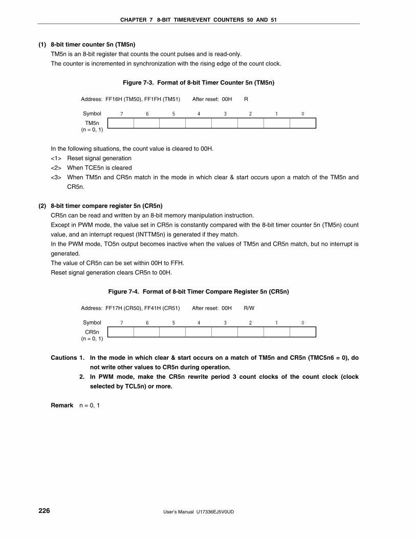
CHAPTER 7 8-BIT TIMER/EVENT COUNTERS 50 AND 51
User’s Manual U17336EJ5V0UD 226
(1) 8-bit timer counter 5n (TM5n)
TM5n is an 8-bit register that counts the count pulses and is read-only.
The counter is incremented in synchronization with the rising edge of the count clock.
Figure 7-3. Format of 8-bit Timer Counter 5n (TM5n)
Symbol
TM5n(n = 0, 1)
Address: FF16H (TM50), FF1FH (TM51) After reset: 00H R
In the following situations, the count value is cleared to 00H.
<1> Reset signal generation
<2> When TCE5n is cleared
<3> When TM5n and CR5n match in the mode in which clear & start occurs upon a match of the TM5n and
CR5n.
(2) 8-bit timer compare register 5n (CR5n)
CR5n can be read and written by an 8-bit memory manipulation instruction.
Except in PWM mode, the value set in CR5n is constantly compared with the 8-bit timer counter 5n (TM5n) count
value, and an interrupt request (INTTM5n) is generated if they match.
In the PWM mode, TO5n output becomes inactive when the values of TM5n and CR5n match, but no interrupt is
generated.
The value of CR5n can be set within 00H to FFH.
Reset signal generation clears CR5n to 00H.
Figure 7-4. Format of 8-bit Timer Compare Register 5n (CR5n)
Symbol
CR5n(n = 0, 1)
Address: FF17H (CR50), FF41H (CR51) After reset: 00H R/W
Cautions 1. In the mode in which clear & start occurs on a match of TM5n and CR5n (TMC5n6 = 0), do
not write other values to CR5n during operation.
2. In PWM mode, make the CR5n rewrite period 3 count clocks of the count clock (clock
selected by TCL5n) or more.
Remark n = 0, 1

CHAPTER 7 8-BIT TIMER/EVENT COUNTERS 50 AND 51
User’s Manual U17336EJ5V0UD 227
7.3 Registers Controlling 8-bit Timer/Event Counters 50 and 51
The following four registers are used to control 8-bit timer/event counters 50 and 51.
• Timer clock selection register 5n (TCL5n)
• 8-bit timer mode control register 5n (TMC5n)
• Port mode register 1 (PM1) or port mode register 3 (PM3)
• Port register 1 (P1) or port register 3 (P3)
(1) Timer clock selection register 5n (TCL5n)
This register sets the count clock of 8-bit timer/event counter 5n and the valid edge of the TI5n pin input.
TCL5n can be set by a 1-bit or 8-bit memory manipulation instruction.
Reset signal generation clears TCL5n to 00H.
Remark n = 0, 1
Figure 7-5. Format of Timer Clock Selection Register 50 (TCL50)
Address: FF6AH After reset: 00H R/W
Symbol 7 6 5 4 3 2 1 0
TCL50 0 0 0 0 0 TCL502 TCL501 TCL500
Count clock selectionNote 1 TCL502 TCL501 TCL500
fPRS =
2 MHz
fPRS =
5 MHz
fPRS =
10 MHz
fPRS =
20 MHz
0 0 0 TI50 pin falling edge
0 0 1 TI50 pin rising edge
0 1 0 fPRSNote 2 2 MHz 5 MHz 10 MHz 20 MHz
0 1 1 fPRS/2 1 MHz 2.5 MHz 5 MHz 10 MHz
1 0 0 fPRS/22 500 kHz 1.25 MHz 2.5 MHz 5 MHz
1 0 1 fPRS/26 31.25 kHz 78.13 kHz 156.25 kHz 312.5 kHz
1 1 0 fPRS/28 7.81 kHz 19.53 kHz 39.06 kHz 78.13 kHz
1 1 1 fPRS/213 0.24 kHz 0.61 kHz 1.22 kHz 2.44 kHz
Notes 1. If the peripheral hardware clock (fPRS) operates on the high-speed system clock (fXH) (XSEL = 1), the
fPRS operating frequency varies depending on the supply voltage.
• VDD = 4.0 to 5.5 V: fPRS ≤ 20 MHz
• VDD = 2.7 to 4.0 V: fPRS ≤ 10 MHz
• VDD = 1.8 to 2.7 V: fPRS ≤ 5 MHz (Standard and (A) grade products only)
2. If the peripheral hardware clock (fPRS) operates on the internal high-speed oscillation clock (fRH) (XSEL
= 0), when 1.8 V ≤ VDD < 2.7 V, the setting of TCL502, TCL501, TCL500 = 0, 1, 0 (count clock: fPRS) is
prohibited.
Cautions 1. When rewriting TCL50 to other data, stop the timer operation beforehand.
2. Be sure to clear bits 3 to 7 to “0”.
Remark fPRS: Peripheral hardware clock frequency
<R>
<R>


CHAPTER 7 8-BIT TIMER/EVENT COUNTERS 50 AND 51
User’s Manual U17336EJ5V0UD 229
(2) 8-bit timer mode control register 5n (TMC5n)
TMC5n is a register that performs the following five types of settings.
<1> 8-bit timer counter 5n (TM5n) count operation control
<2> 8-bit timer counter 5n (TM5n) operating mode selection
<3> Timer output F/F (flip flop) status setting
<4> Active level selection in timer F/F control or PWM (free-running) mode.
<5> Timer output control
TMC5n can be set by a 1-bit or 8-bit memory manipulation instruction.
Reset signal generation clears this register to 00H.
Remark n = 0, 1
Figure 7-7. Format of 8-bit Timer Mode Control Register 50 (TMC50)
Address: FF6BH After reset: 00H R/WNote
Symbol <7> 6 5 4 <3> <2> 1 <0>
TMC50 TCE50 TMC506 0 0 LVS50 LVR50 TMC501 TOE50
TCE50 TM50 count operation control
0 After clearing to 0, count operation disabled (counter stopped)
1 Count operation start
TMC506 TM50 operating mode selection
0 Mode in which clear & start occurs on a match between TM50 and CR50
1 PWM (free-running) mode
LVS50 LVR50 Timer output F/F status setting
0 0 No change
0 1 Timer output F/F clear (0) (default value of TO50 output: low level)
1 0 Timer output F/F set (1) (default value of TO50 output: high level)
1 1 Setting prohibited
In other modes (TMC506 = 0) In PWM mode (TMC506 = 1) TMC501
Timer F/F control Active level selection
0 Inversion operation disabled Active-high
1 Inversion operation enabled Active-low
TOE50 Timer output control
0 Output disabled (TO50 output is low level)
1 Output enabled
Note Bits 2 and 3 are write-only.
(Cautions and Remarks are listed on the next page.)
<R>
<R>

CHAPTER 7 8-BIT TIMER/EVENT COUNTERS 50 AND 51
User’s Manual U17336EJ5V0UD 230
Figure 7-8. Format of 8-bit Timer Mode Control Register 51 (TMC51)
Address: FF43H After reset: 00H R/WNote
Symbol <7> 6 5 4 <3> <2> 1 <0>
TMC51 TCE51 TMC516 0 0 LVS51 LVR51 TMC511 TOE51
TCE51 TM51 count operation control
0 After clearing to 0, count operation disabled (counter stopped)
1 Count operation start
TMC516 TM51 operating mode selection
0 Mode in which clear & start occurs on a match between TM51 and CR51
1 PWM (free-running) mode
LVS51 LVR51 Timer output F/F status setting
0 0 No change
0 1 Timer output F/F clear (0) (default value of TO51 output: low level)
1 0 Timer output F/F set (1) (default value of TO51 output: high level)
1 1 Setting prohibited
In other modes (TMC516 = 0) In PWM mode (TMC516 = 1) TMC511
Timer F/F control Active level selection
0 Inversion operation disabled Active-high
1 Inversion operation enabled Active-low
TOE51 Timer output control
0 Output disabled (TO51 output is low level)
1 Output enabled
Note Bits 2 and 3 are write-only.
Cautions 1. The settings of LVS5n and LVR5n are valid in other than PWM mode.
2. Perform <1> to <4> below in the following order, not at the same time.
<1> Set TMC5n1, TMC5n6: Operation mode setting
<2> Set TOE5n to enable output: Timer output enable
<3> Set LVS5n, LVR5n (see Caution 1): Timer F/F setting
<4> Set TCE5n
3. When TCE5n = 1, setting the other bits of TMC5n is prohibited.
4. The actual TO50/TI50/P17 and TO51/TI51/P33/INTP4 pin outputs are determined depending on
PM17 and P17, and PM33 and P33, besides TO5n output.
Remarks 1. In PWM mode, PWM output is made inactive by clearing TCE5n to 0.
2. If LVS5n and LVR5n are read, the value is 0.
3. The values of the TMC5n6, LVS5n, LVR5n, TMC5n1, and TOE5n bits are reflected in TO5n output
regardless of the value of TCE5n.
4. n = 0, 1
<R>
<R>
<R>
<R>

CHAPTER 7 8-BIT TIMER/EVENT COUNTERS 50 AND 51
User’s Manual U17336EJ5V0UD 231
(3) Port mode registers 1 and 3 (PM1, PM3)
These registers set port 1 and 3 input/output in 1-bit units.
When using the P17/TO50/TI50 and P33/TO51/TI51/INTP4 pins for timer output, clear PM17 and PM33 and the
output latches of P17 and P33 to 0.
When using the P17/TO50/TI50 and P33/TO51/TI51/INTP4 pins for timer input, set PM17 and PM33 to 1. The
output latches of P17 and P33 at this time may be 0 or 1.
PM1 and PM3 can be set by a 1-bit or 8-bit memory manipulation instruction.
Reset signal generation sets these registers to FFH.
Figure 7-9. Format of Port Mode Register 1 (PM1)
Address: FF21H After reset: FFH R/W
Symbol 7 6 5 4 3 2 1 0
PM1 PM17 PM16 PM15 PM14 PM13 PM12 PM11 PM10
PM1n P1n pin I/O mode selection (n = 0 to 7)
0 Output mode (output buffer on)
1 Input mode (output buffer off)
Figure 7-10. Format of Port Mode Register 3 (PM3)
Address: FF23H After reset: FFH R/W
Symbol 7 6 5 4 3 2 1 0
PM3 1 1 1 1 PM33 PM32 PM31 PM30
PM3n P3n pin I/O mode selection (n = 0 to 3)
0 Output mode (output buffer on)
1 Input mode (output buffer off)

CHAPTER 7 8-BIT TIMER/EVENT COUNTERS 50 AND 51
User’s Manual U17336EJ5V0UD 232
7.4 Operations of 8-bit Timer/Event Counters 50 and 51
7.4.1 Operation as interval timer
8-bit timer/event counter 5n operates as an interval timer that generates interrupt requests repeatedly at intervals
of the count value preset to 8-bit timer compare register 5n (CR5n).
When the count value of 8-bit timer counter 5n (TM5n) matches the value set to CR5n, counting continues with the
TM5n value cleared to 0 and an interrupt request signal (INTTM5n) is generated.
The count clock of TM5n can be selected with bits 0 to 2 (TCL5n0 to TCL5n2) of timer clock selection register 5n
(TCL5n).
Setting
<1> Set the registers.
• TCL5n: Select the count clock.
• CR5n: Compare value
• TMC5n: Stop the count operation, select the mode in which clear & start occurs on a match of TM5n
and CR5n.
(TMC5n = 0000×××0B × = Don’t care)
<2> After TCE5n = 1 is set, the count operation starts.
<3> If the values of TM5n and CR5n match, INTTM5n is generated (TM5n is cleared to 00H).
<4> INTTM5n is generated repeatedly at the same interval.
Set TCE5n to 0 to stop the count operation.
Caution Do not write other values to CR5n during operation.
Remarks 1. For how to enable the INTTM5n signal interrupt, see CHAPTER 18 INTERRUPT FUNCTIONS.
2. n = 0, 1
Figure 7-11. Interval Timer Operation Timing (1/2)
(a) Basic operation
t
Count clock
TM5n count value
CR5n
TCE5n
INTTM5n
Count start Clear Clear
00H 01H N 00H 01H N 00H 01H N
NNNN
Interrupt acknowledged Interrupt acknowledged
Interval timeInterval time
Remark Interval time = (N + 1) × t
N = 01H to FFH
n = 0, 1
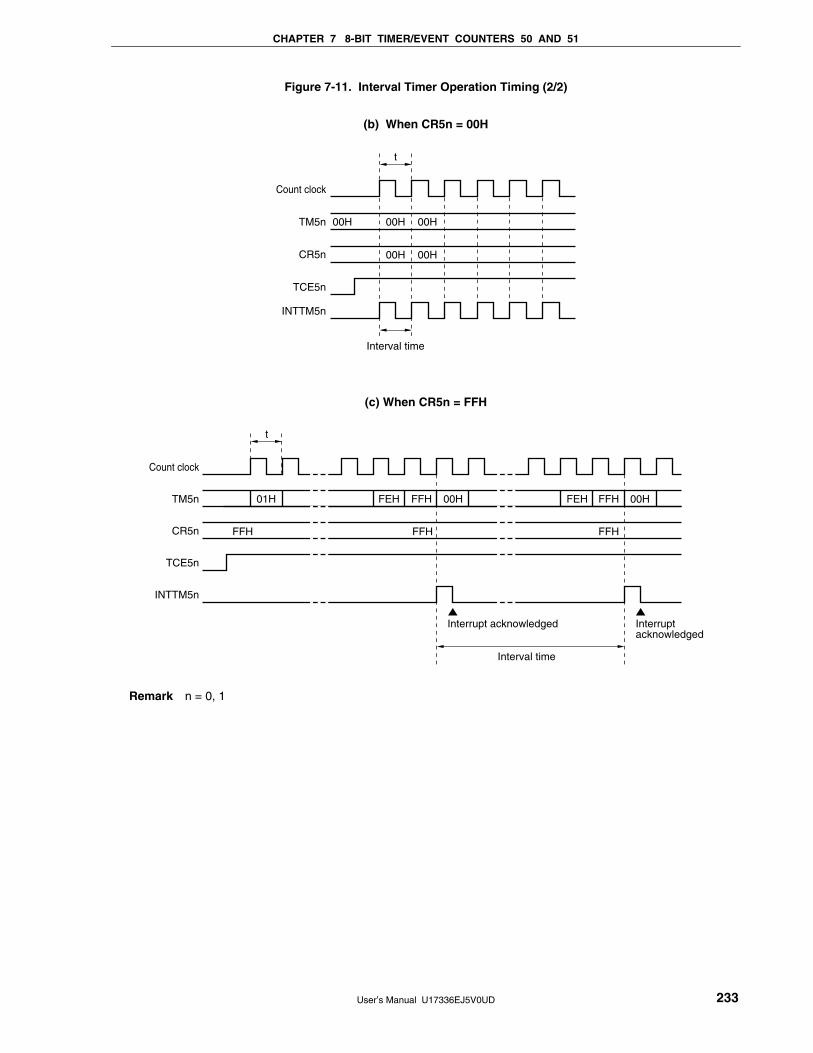
CHAPTER 7 8-BIT TIMER/EVENT COUNTERS 50 AND 51
User’s Manual U17336EJ5V0UD 233
Figure 7-11. Interval Timer Operation Timing (2/2)
(b) When CR5n = 00H
t
Interval time
Count clock
TM5n
CR5n
TCE5n
INTTM5n
00H 00H 00H
00H 00H
(c) When CR5n = FFH
t
Count clock
TM5n
CR5n
TCE5n
INTTM5n
01H FEH FFH 00H FEH FFH 00H
FFHFFHFFH
Interval time
Interrupt acknowledged
Interrupt acknowledged
Remark n = 0, 1

CHAPTER 7 8-BIT TIMER/EVENT COUNTERS 50 AND 51
User’s Manual U17336EJ5V0UD 234
7.4.2 Operation as external event counter
The external event counter counts the number of external clock pulses to be input to the TI5n pin by 8-bit timer
counter 5n (TM5n).
TM5n is incremented each time the valid edge specified by timer clock selection register 5n (TCL5n) is input.
Either the rising or falling edge can be selected.
When the TM5n count value matches the value of 8-bit timer compare register 5n (CR5n), TM5n is cleared to 0
and an interrupt request signal (INTTM5n) is generated.
Whenever the TM5n value matches the value of CR5n, INTTM5n is generated.
Setting
<1> Set each register.
• Set the port mode register (PM17 or PM33)Note to 1.
• TCL5n: Select TI5n pin input edge.
TI5n pin falling edge → TCL5n = 00H
TI5n pin rising edge → TCL5n = 01H
• CR5n: Compare value
• TMC5n: Stop the count operation, select the mode in which clear & start occurs on match of TM5n and
CR5n, disable the timer F/F inversion operation, disable timer output.
(TMC5n = 00000000B)
<2> When TCE5n = 1 is set, the number of pulses input from the TI5n pin is counted.
<3> When the values of TM5n and CR5n match, INTTM5n is generated (TM5n is cleared to 00H).
<4> After these settings, INTTM5n is generated each time the values of TM5n and CR5n match.
Note 8-bit timer/event counter 50: PM17
8-bit timer/event counter 51: PM33
Remark For how to enable the INTTM5n signal interrupt, see CHAPTER 18 INTERRUPT FUNCTIONS.
Figure 7-12. External Event Counter Operation Timing (with Rising Edge Specified)
TI5n
TM5n count value
CR5n
INTTM5n
00H 01H 02H 03H 04H 05H N − 1 N 00H 01H 02H 03H
N
Count start
Remark N = 00H to FFH
n = 0, 1

CHAPTER 7 8-BIT TIMER/EVENT COUNTERS 50 AND 51
User’s Manual U17336EJ5V0UD 235
7.4.3 Square-wave output operation
A square wave with any selected frequency is output at intervals determined by the value preset to 8-bit timer
compare register 5n (CR5n).
The TO5n output status is inverted at intervals determined by the count value preset to CR5n by setting bit 0
(TOE5n) of 8-bit timer mode control register 5n (TMC5n) to 1. This enables a square wave with any selected
frequency to be output (duty = 50%).
Setting
<1> Set each register.
• Clear the port output latch (P17 or P33)Note and port mode register (PM17 or PM33)Note to 0.
• TCL5n: Select the count clock.
• CR5n: Compare value
• TMC5n: Stop the count operation, select the mode in which clear & start occurs on a match of TM5n and
CR5n.
LVS5n LVR5n Timer Output F/F Status Setting
0 1 Timer output F/F clear (0) (default value of TO5n output: low level)
1 0 Timer output F/F set (1) (default value of TO5n output: high level)
Timer output enabled
(TMC5n = 00001011B or 00000111B)
<2> After TCE5n = 1 is set, the count operation starts.
<3> The timer output F/F is inverted by a match of TM5n and CR5n. After INTTM5n is generated, TM5n is
cleared to 00H.
<4> After these settings, the timer output F/F is inverted at the same interval and a square wave is output from
TO5n.
The frequency is as follows.
• Frequency = 1/2t (N + 1)
(N: 00H to FFH)
Note 8-bit timer/event counter 50: P17, PM17
8-bit timer/event counter 51: P33, PM33
Caution Do not write other values to CR5n during operation.
Remarks 1. For how to enable the INTTM5n signal interrupt, see CHAPTER 18 INTERRUPT FUNCTIONS.
2. n = 0, 1

CHAPTER 7 8-BIT TIMER/EVENT COUNTERS 50 AND 51
User’s Manual U17336EJ5V0UD 236
Figure 7-13. Square-Wave Output Operation Timing
Count clock
TM5n count value 00H 01H 02H N − 1 N
N
00H N − 1 N 00H01H 02H
CR5n
TO5nNote
t
Count start
Note The initial value of TO5n output can be set by bits 2 and 3 (LVR5n, LVS5n) of 8-bit timer mode control
register 5n (TMC5n).
7.4.4 PWM output operation
8-bit timer/event counter 5n operates as a PWM output when bit 6 (TMC5n6) of 8-bit timer mode control register 5n
(TMC5n) is set to 1.
The duty pulse determined by the value set to 8-bit timer compare register 5n (CR5n) is output from TO5n.
Set the active level width of the PWM pulse to CR5n; the active level can be selected with bit 1 (TMC5n1) of
TMC5n.
The count clock can be selected with bits 0 to 2 (TCL5n0 to TCL5n2) of timer clock selection register 5n (TCL5n).
PWM output can be enabled/disabled with bit 0 (TOE5n) of TMC5n.
Caution In PWM mode, make the CR5n rewrite period 3 count clocks of the count clock (clock selected by
TCL5n) or more.
Remark n = 0, 1

CHAPTER 7 8-BIT TIMER/EVENT COUNTERS 50 AND 51
User’s Manual U17336EJ5V0UD 237
(1) PWM output basic operation
Setting
<1> Set each register.
• Clear the port output latch (P17 or P33)Note and port mode register (PM17 or PM33)Note to 0.
• TCL5n: Select the count clock.
• CR5n: Compare value
• TMC5n: Stop the count operation, select PWM mode.
The timer output F/F is not changed.
TMC5n1 Active Level Selection
0 Active-high
1 Active-low
Timer output enabled
(TMC5n = 01000001B or 01000011B)
<2> The count operation starts when TCE5n = 1.
Clear TCE5n to 0 to stop the count operation.
Note 8-bit timer/event counter 50: P17, PM17
8-bit timer/event counter 51: P33, PM33
PWM output operation
<1> PWM output (TO5n output) outputs an inactive level until an overflow occurs.
<2> When an overflow occurs, the active level is output. The active level is output until CR5n matches the count
value of 8-bit timer counter 5n (TM5n).
<3> After the CR5n matches the count value, the inactive level is output until an overflow occurs again.
<4> Operations <2> and <3> are repeated until the count operation stops.
<5> When the count operation is stopped with TCE5n = 0, PWM output becomes inactive.
For details of timing, see Figures 7-14 and 7-15.
The cycle, active-level width, and duty are as follows.
• Cycle = 28t
• Active-level width = Nt
• Duty = N/28
(N = 00H to FFH)
Remark n = 0, 1

CHAPTER 7 8-BIT TIMER/EVENT COUNTERS 50 AND 51
User’s Manual U17336EJ5V0UD 238
Figure 7-14. PWM Output Operation Timing
(a) Basic operation (active level = H)
Count clock
TM5n
CR5n
TCE5n
INTTM5n
TO5n
00H 01H FFH 00H 01H 02H N N + 1 FFH 00H 01H 02H M 00H
N
<2> Active level<1> Inactive level <3> Inactive level <5> Inactive level
t
<2> Active level
(b) CR5n = 00H
Count clock
TM5n
CR5n
TCE5n
INTTM5n
01H00H FFH 00H 01H 02H
00H
FFH 00H 01H 02H M 00H
TO5n L (Inactive level)
t
(c) CR5n = FFH
TM5n
CR5n
TCE5n
INTTM5n
TO5n
01H00H FFH 00H 01H 02H
FFH
<1> Inactive level <2> Active level
FFH 00H 01H 02H M 00H
<3> Inactive level
<2> Active level<5> Inactive level
t
Remarks 1. <1> to <3> and <5> in Figure 7-14 (a) correspond to <1> to <3> and <5> in PWM output operation in
7.4.4 (1) PWM output basic operation.
2. n = 0, 1

CHAPTER 7 8-BIT TIMER/EVENT COUNTERS 50 AND 51
User’s Manual U17336EJ5V0UD 239
(2) Operation with CR5n changed
Figure 7-15. Timing of Operation with CR5n Changed
(a) CR5n value is changed from N to M before clock rising edge of FFH
→ Value is transferred to CR5n at overflow immediately after change.
Count clock
TM5n
CR5n
TCE5nINTTM5n
TO5n
<1> CR5n change (N → M)
N N + 1 N + 2 FFH 00H 01H M M + 1 M + 2 FFH 00H 01H 02H M M + 1 M + 2
N
02H
M
H
<2>
t
(b) CR5n value is changed from N to M after clock rising edge of FFH
→ Value is transferred to CR5n at second overflow.
Count clock
TM5n
CR5n
TCE5nINTTM5n
TO5n
N N + 1 N + 2 FFH 00H 01H N N + 1 N + 2 FFH 00H 01H 02H
N
02H
N
H
M
M M + 1 M + 2
<1> CR5n change (N → M) <2>
t
Caution When reading from CR5n between <1> and <2> in Figure 7-15, the value read differs from the
actual value (read value: M, actual value of CR5n: N).

CHAPTER 7 8-BIT TIMER/EVENT COUNTERS 50 AND 51
User’s Manual U17336EJ5V0UD 240
7.5 Cautions for 8-bit Timer/Event Counters 50 and 51
(1) Timer start error
An error of up to one clock may occur in the time required for a match signal to be generated after timer start.
This is because 8-bit timer counters 50 and 51 (TM50, TM51) are started asynchronously to the count clock.
Figure 7-16. 8-bit Timer Counter 5n Start Timing
Count clock
TM5n count value 00H 01H 02H 03H 04H
Timer start
Remark n = 0, 1

User’s Manual U17336EJ5V0UD 241
CHAPTER 8 8-BIT TIMERS H0 AND H1
8.1 Functions of 8-bit Timers H0 and H1
8-bit timers H0 and H1 have the following functions.
• Interval timer
• Square-wave output
• PWM output
• Carrier generator (8-bit timer H1 only)
8.2 Configuration of 8-bit Timers H0 and H1
8-bit timers H0 and H1 include the following hardware.
Table 8-1. Configuration of 8-bit Timers H0 and H1
Item Configuration
Timer register 8-bit timer counter Hn
Registers 8-bit timer H compare register 0n (CMP0n)
8-bit timer H compare register 1n (CMP1n)
Timer output TOHn, output controller
Control registers 8-bit timer H mode register n (TMHMDn)
8-bit timer H carrier control register 1 (TMCYC1)Note
Port mode register 1 (PM1)
Port register 1 (P1)
Note 8-bit timer H1 only
Remark n = 0, 1
Figures 8-1 and 8-2 show the block diagrams.

CH
AP
TE
R 8 8-B
IT T
IME
RS
H0 A
ND
H1
User’s M
anual U17336E
J5V0U
D
242 <R> Figure 8-1. Block Diagram of 8-bit Timer H0
TMHE0 CKS02 CKS01 CKS00 TMMD01 TMMD00 TOLEV0 TOEN0
TOH0/P15
TOH0output
INTTMH0
fPRS
fPRS/2fPRS/22
fPRS/26
fPRS/210
10
F/F
R
3 2
PM15Match
Internal bus
8-bit timer H mode register 0 (TMHMD0)
8-bit timer H compare register
10 (CMP10)
Decoder
Selector
Interrupt generator
Output controller
Levelinversion
PWM mode signal
Timer H enable signal
Clear
8-bit timer H compare register
00 (CMP00)
Output latch(P15)
8-bit timer/event counter 50 output
Sel
ecto
r
8-bit timercounter H0

CH
AP
TE
R 8 8-B
IT T
IME
RS
H0 A
ND
H1
User’s M
anual U17336E
J5V0U
D
243
<R> Figure 8-2. Block Diagram of 8-bit Timer H1
Match
Internal bus
TMHE1 CKS12 CKS11 CKS10 TMMD11 TMMD10 TOLEV1 TOEN1 8-bit timer Hcompare
register 11(CMP11)
Decoder
TOH1/INTP5/P16
8-bit timer H carrier control register 1(TMCYC1)
INTTMH1
INTTM51
TOH1output
Selector
fPRS
fPRS/22
fPRS/24
fPRS/26
fPRS/212
fRL
fRL/27
fRL/29
Interruptgenerator
Outputcontroller
Levelinversion PM16Output latch
(P16)
10
F/F
R
PWM mode signal
Carrier generator mode signal
Timer H enable signal
3 2
8-bit timer Hcompare
register 01(CMP01)
8-bit timercounter H1
Clear
RMC1 NRZB1 NRZ1
Reload/interrupt control
8-bit timer H mode register 1 (TMHMD1)
Sel
ecto
r

CHAPTER 8 8-BIT TIMERS H0 AND H1
User’s Manual U17336EJ5V0UD 244
(1) 8-bit timer H compare register 0n (CMP0n)
This register can be read or written by an 8-bit memory manipulation instruction. This register is used in all of the
timer operation modes.
This register constantly compares the value set to CMP0n with the count value of 8-bit timer counter Hn and,
when the two values match, generates an interrupt request signal (INTTMHn) and inverts the output level of
TOHn.
Rewrite the value of CMP0n while the timer is stopped (TMHEn = 0).
A reset signal generation clears this register to 00H.
Figure 8-3. Format of 8-bit Timer H Compare Register 0n (CMP0n)
Symbol
CMP0n(n = 0, 1)
Address: FF18H (CMP00), FF1AH (CMP01) After reset: 00H R/W
7 6 5 4 3 2 1 0
Caution CMP0n cannot be rewritten during timer count operation. CMP0n can be refreshed (the same
value is written) during timer count operation.
(2) 8-bit timer H compare register 1n (CMP1n)
This register can be read or written by an 8-bit memory manipulation instruction. This register is used in the
PWM output mode and carrier generator mode.
In the PWM output mode, this register constantly compares the value set to CMP1n with the count value of 8-bit
timer counter Hn and, when the two values match, inverts the output level of TOHn. No interrupt request signal is
generated.
In the carrier generator mode, the CMP1n register always compares the value set to CMP1n with the count value
of 8-bit timer counter Hn and, when the two values match, generates an interrupt request signal (INTTMHn). At
the same time, the count value is cleared.
CMP1n can be refreshed (the same value is written) and rewritten during timer count operation.
If the value of CMP1n is rewritten while the timer is operating, the new value is latched and transferred to CMP1n
when the count value of the timer matches the old value of CMP1n, and then the value of CMP1n is changed to
the new value. If matching of the count value and the CMP1n value and writing a value to CMP1n conflict, the
value of CMP1n is not changed.
A reset signal generation clears this register to 00H.
Figure 8-4. Format of 8-bit Timer H Compare Register 1n (CMP1n)
Symbol
CMP1n(n = 0, 1)
Address: FF19H (CMP10), FF1BH (CMP11) After reset: 00H R/W
7 6 5 4 3 2 1 0
Caution In the PWM output mode and carrier generator mode, be sure to set CMP1n when starting the
timer count operation (TMHEn = 1) after the timer count operation was stopped (TMHEn = 0) (be
sure to set again even if setting the same value to CMP1n).
Remark n = 0, 1

CHAPTER 8 8-BIT TIMERS H0 AND H1
User’s Manual U17336EJ5V0UD 245
8.3 Registers Controlling 8-bit Timers H0 and H1
The following four registers are used to control 8-bit timers H0 and H1.
• 8-bit timer H mode register n (TMHMDn)
• 8-bit timer H carrier control register 1 (TMCYC1)Note
• Port mode register 1 (PM1)
• Port register 1 (P1)
Note 8-bit timer H1 only
(1) 8-bit timer H mode register n (TMHMDn)
This register controls the mode of timer H.
This register can be set by a 1-bit or 8-bit memory manipulation instruction.
Reset signal generation clears this register to 00H.
Remark n = 0, 1

CHAPTER 8 8-BIT TIMERS H0 AND H1
User’s Manual U17336EJ5V0UD 246
Figure 8-5. Format of 8-bit Timer H Mode Register 0 (TMHMD0)
TMHE0
Stops timer count operation (counter is cleared to 0)
Enables timer count operation (count operation started by inputting clock)
TMHE0
0
1
Timer operation enable
TMHMD0 CKS02 CKS01 CKS00 TMMD01 TMMD00 TOLEV0 TOEN0
Address: FF69H After reset: 00H R/W
Symbol
fPRSNote 2
fPRS/2
fPRS/22
fPRS/26
fPRS/210
TM50 outputNote 3
Setting prohibited
CKS02
0
0
0
0
1
1
CKS01
0
0
1
1
0
0
CKS00
0
1
0
1
0
1
fPRS = 2 MHz
2 MHz
1 MHz
500 kHz
31.25 kHz
1.95 kHz
Count clock selectionNote 1
Other than above
Interval timer mode
PWM output mode
Setting prohibited
TMMD01
0
1
TMMD00
0
0
Timer operation mode
Low level
High level
TOLEV0
0
1
Timer output level control (in default mode)
Disables output
Enables output
TOEN0
0
1
Timer output control
Other than above
<7> 6 5 4 3 2 <1> <0>
fPRS = 5 MHz
5 MHz
2.5 MHz
1.25 MHz
78.13 kHz
4.88 kHz
fPRS = 10 MHz
10 MHz
5 MHz
2.5 MHz
156.25 kHz
9.77 kHz
fPRS = 20 MHz
20 MHz
10 MHz
5 MHz
312.5 kHz
19.54 kHz
Notes 1. If the peripheral hardware clock (fPRS) operates on the high-speed system clock (fXH) (XSEL = 1), the
fPRS operating frequency varies depending on the supply voltage.
• VDD = 4.0 to 5.5 V: fPRS ≤ 20 MHz
• VDD = 2.7 to 4.0 V: fPRS ≤ 10 MHz
• VDD = 1.8 to 2.7 V: fPRS ≤ 5 MHz (Standard and (A) grade products only)
2. If the peripheral hardware clock (fPRS) operates on the internal high-speed oscillation clock (fRH) (XSEL
= 0), when 1.8 V ≤ VDD < 2.7 V, the setting of CKS02 = CKS01 = CKS00 = 0 (count clock: fPRS) is
prohibited.
<R>
<R>
CHAPTER 8 8-BIT TIMERS H0 AND H1
User’s Manual U17336EJ5V0UD 247
Note 3. Note the following points when selecting the TM50 output as the count clock.
• Mode in which the count clock is cleared and started upon a match of TM50 and CR50 (TMC506 = 0)
Start the operation of 8-bit timer/event counter 50 first and then enable the timer F/F inversion
operation (TMC501 = 1).
• PWM mode (TMC506 = 1)
Start the operation of 8-bit timer/event counter 50 first and then set the count clock to make the duty =
50%.
It is not necessary to enable (TOE50 = 1) TO50 output in any mode.
Cautions 1. When TMHE0 = 1, setting the other bits of TMHMD0 is prohibited. However, TMHMD0 can be
refreshed (the same value is written).
2. In the PWM output mode, be sure to set 8-bit timer H compare register 10 (CMP10) when
starting the timer count operation (TMHE0 = 1) after the timer count operation was stopped
(TMHE0 = 0) (be sure to set again even if setting the same value to CMP10).
3. The actual TOH0/P15 pin output is determined depending on PM15 and P15, besides TOH0
output.
Remarks 1. fPRS: Peripheral hardware clock frequency
2. TMC506: Bit 6 of 8-bit timer mode control register 50 (TMC50)
TMC501: Bit 1 of TMC50
<R>
<R>

CHAPTER 8 8-BIT TIMERS H0 AND H1
User’s Manual U17336EJ5V0UD 248
Figure 8-6. Format of 8-bit Timer H Mode Register 1 (TMHMD1)
TMHE1
Stops timer count operation (counter is cleared to 0)
Enables timer count operation (count operation started by inputting clock)
TMHE1
0
1
Timer operation enable
TMHMD1 CKS12 CKS11 CKS10 TMMD11 TMMD10 TOLEV1 TOEN1
Address: FF6CH After reset: 00H R/W
Symbol
Interval timer mode
Carrier generator mode
PWM output mode
Setting prohibited
TMMD11
0
0
1
1
TMMD10
0
1
0
1
Timer operation mode
Low level
High level
TOLEV1
0
1
Timer output level control (in default mode)
Disables output
Enables output
TOEN1
0
1
Timer output control
<7> 6 5 4 3 2 <1> <0>
fPRSNote 2
fPRS/22
fPRS/24
fPRS/26
fPRS/212
fRL/27
fRL/29
fRL
CKS12
0
0
0
0
1
1
1
1
CKS11
0
0
1
1
0
0
1
1
CKS10
0
1
0
1
0
1
0
1
fPRS = 2 MHz
2 MHz
500 kHz
125 kHz
31.25 kHz
0.49 kHz
1.88 kHz (TYP.)
0.47 kHz (TYP.)
240 kHz (TYP.)
Count clock selectionNote 1
fPRS = 5 MHz
5 MHz
1.25 MHz
312.5 kHz
78.13 kHz
1.22 kHz
fPRS = 10 MHz
10 MHz
2.5 MHz
625 kHz
156.25 kHz
2.44 kHz
fPRS = 20 MHz
20 MHz
5 MHz
1.25 MHz
312.5 kHz
4.88 kHz
Notes 1. If the peripheral hardware clock (fPRS) operates on the high-speed system clock (fXH) (XSEL = 1), the
fPRS operating frequency varies depending on the supply voltage.
• VDD = 4.0 to 5.5 V: fPRS ≤ 20 MHz
• VDD = 2.7 to 4.0 V: fPRS ≤ 10 MHz
• VDD = 1.8 to 2.7 V: fPRS ≤ 5 MHz (Standard and (A) grade products only)
2. If the peripheral hardware clock (fPRS) operates on the internal high-speed oscillation clock (fRH) (XSEL
= 0), when 1.8 V ≤ VDD < 2.7 V, the setting of CKS12 = CKS11 = CKS10 = 0 (count clock: fPRS) is
prohibited.
<R>
<R>
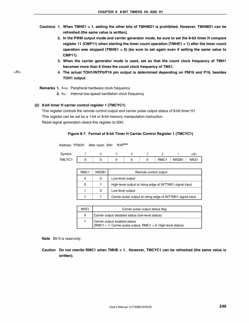
CHAPTER 8 8-BIT TIMERS H0 AND H1
User’s Manual U17336EJ5V0UD 249
Cautions 1. When TMHE1 = 1, setting the other bits of TMHMD1 is prohibited. However, TMHMD1 can be
refreshed (the same value is written).
2. In the PWM output mode and carrier generator mode, be sure to set the 8-bit timer H compare
register 11 (CMP11) when starting the timer count operation (TMHE1 = 1) after the timer count
operation was stopped (TMHE1 = 0) (be sure to set again even if setting the same value to
CMP11).
3. When the carrier generator mode is used, set so that the count clock frequency of TMH1
becomes more than 6 times the count clock frequency of TM51.
4. The actual TOH1/INTP5/P16 pin output is determined depending on PM16 and P16, besides
TOH1 output.
Remarks 1. fPRS: Peripheral hardware clock frequency
2. fRL: Internal low-speed oscillation clock frequency
(2) 8-bit timer H carrier control register 1 (TMCYC1)
This register controls the remote control output and carrier pulse output status of 8-bit timer H1.
This register can be set by a 1-bit or 8-bit memory manipulation instruction.
Reset signal generation clears this register to 00H.
Figure 8-7. Format of 8-bit Timer H Carrier Control Register 1 (TMCYC1)
0TMCYC1 0 0 0 0 RMC1 NRZB1 NRZ1
Address: FF6DH After reset: 00H R/WNote
Symbol
Low-level output
High-level output at rising edge of INTTM51 signal input
Low-level output
Carrier pulse output at rising edge of INTTM51 signal input
RMC1
0
0
1
1
NRZB1
0
1
0
1
Remote control output
Carrier output disabled status (low-level status)
Carrier output enabled status (RMC1 = 1: Carrier pulse output, RMC1 = 0: High-level status)
NRZ1
0
1
Carrier pulse output status flag
<0>
Note Bit 0 is read-only.
Caution Do not rewrite RMC1 when TMHE = 1. However, TMCYC1 can be refreshed (the same value is
written).
<R>

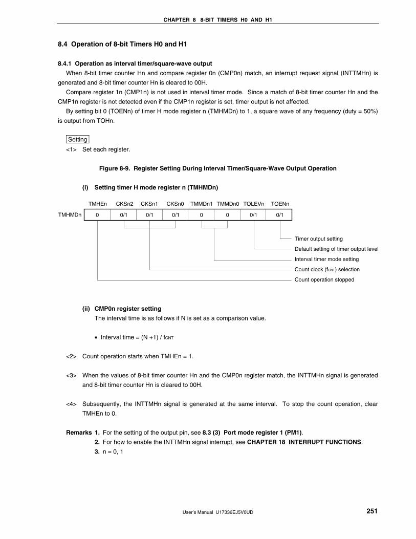
CHAPTER 8 8-BIT TIMERS H0 AND H1
User’s Manual U17336EJ5V0UD 251
8.4 Operation of 8-bit Timers H0 and H1
8.4.1 Operation as interval timer/square-wave output
When 8-bit timer counter Hn and compare register 0n (CMP0n) match, an interrupt request signal (INTTMHn) is
generated and 8-bit timer counter Hn is cleared to 00H.
Compare register 1n (CMP1n) is not used in interval timer mode. Since a match of 8-bit timer counter Hn and the
CMP1n register is not detected even if the CMP1n register is set, timer output is not affected.
By setting bit 0 (TOENn) of timer H mode register n (TMHMDn) to 1, a square wave of any frequency (duty = 50%)
is output from TOHn.
Setting
<1> Set each register.
Figure 8-9. Register Setting During Interval Timer/Square-Wave Output Operation
(i) Setting timer H mode register n (TMHMDn)
0 0/1 0/1 0/1 0 0 0/1 0/1
TMMDn0 TOLEVn TOENnCKSn1CKSn2TMHEn
TMHMDn
CKSn0 TMMDn1
Timer output setting
Default setting of timer output level
Interval timer mode setting
Count clock (fCNT) selection
Count operation stopped
(ii) CMP0n register setting
The interval time is as follows if N is set as a comparison value.
• Interval time = (N +1) / fCNT
<2> Count operation starts when TMHEn = 1.
<3> When the values of 8-bit timer counter Hn and the CMP0n register match, the INTTMHn signal is generated
and 8-bit timer counter Hn is cleared to 00H.
<4> Subsequently, the INTTMHn signal is generated at the same interval. To stop the count operation, clear
TMHEn to 0.
Remarks 1. For the setting of the output pin, see 8.3 (3) Port mode register 1 (PM1).
2. For how to enable the INTTMHn signal interrupt, see CHAPTER 18 INTERRUPT FUNCTIONS.
3. n = 0, 1

CHAPTER 8 8-BIT TIMERS H0 AND H1
User’s Manual U17336EJ5V0UD 252
Figure 8-10. Timing of Interval Timer/Square-Wave Output Operation (1/2)
(a) Basic operation (Operation When 01H ≤ CMP0n ≤ FEH)
00H
Count clock
Count start
8-bit timer counter Hn
CMP0n
TMHEn
INTTMHn
TOHn
01H N
Clear
Interval time
Clear
N
00H 01H N 00H 01H 00H
<2> Level inversion,
match interrupt occurrence,8-bit timer counter Hn clear
<2> Level inversion,
match interrupt occurrence,8-bit timer counter Hn clear
<3><1>
<1> The count operation is enabled by setting the TMHEn bit to 1. The count clock starts counting no more than
1 clock after the operation is enabled.
<2> When the value of the 8-bit timer counter Hn matches the value of the CMP0n register, the value of the timer
counter is cleared, and the level of the TOHn output is inverted. In addition, the INTTMHn signal is output at
the rising edge of the count clock.
<3> If the TMHEn bit is cleared to 0 while timer H is operating, the INTTMHn signal and TOHn output are set to
the default level. If they are already at the default level before the TMHEn bit is cleared to 0, then that level
is maintained.
Remark n = 0, 1
01H ≤ N ≤ FEH

CHAPTER 8 8-BIT TIMERS H0 AND H1
User’s Manual U17336EJ5V0UD 253
Figure 8-10. Timing of Interval Timer/Square-Wave Output Operation (2/2)
(b) Operation when CMP0n = FFH
00H
Count clock
Count start
8-bit timer counter Hn
CMP0n
TMHEn
INTTMHn
TOHn
01H FEH
ClearClear
FFH 00H FEH FFH 00H
FFH
Interval time
(c) Operation when CMP0n = 00H
00H
00H
Count clock
Count start
8-bit timer counter Hn
CMP0n
TMHEn
INTTMHn
TOHn
Interval time
Remark n = 0, 1

CHAPTER 8 8-BIT TIMERS H0 AND H1
User’s Manual U17336EJ5V0UD 254
8.4.2 Operation as PWM output
In PWM output mode, a pulse with an arbitrary duty and arbitrary cycle can be output.
8-bit timer compare register 0n (CMP0n) controls the cycle of timer output (TOHn). Rewriting the CMP0n register
during timer operation is prohibited.
8-bit timer compare register 1n (CMP1n) controls the duty of timer output (TOHn). Rewriting the CMP1n register
during timer operation is possible.
The operation in PWM output mode is as follows.
PWM output (TOHn output) outputs an active level and 8-bit timer counter Hn is cleared to 0 when 8-bit timer
counter Hn and the CMP0n register match after the timer count is started. PWM output (TOHn output) outputs an
inactive level when 8-bit timer counter Hn and the CMP1n register match.
Setting
<1> Set each register.
Figure 8-11. Register Setting in PWM Output Mode
(i) Setting timer H mode register n (TMHMDn)
0 0/1 0/1 0/1 1 0 0/1 1
TMMDn0 TOLEVn TOENnCKSn1CKSn2TMHEn
TMHMDn
CKSn0 TMMDn1
Timer output enabled
Default setting of timer output level
PWM output mode selection
Count clock (fCNT) selection
Count operation stopped
(ii) Setting CMP0n register
• Compare value (N): Cycle setting
(iii) Setting CMP1n register
• Compare value (M): Duty setting
Remarks 1. n = 0, 1
2. 00H ≤ CMP1n (M) < CMP0n (N) ≤ FFH
<2> The count operation starts when TMHEn = 1.
<3> The CMP0n register is the compare register that is to be compared first after counter operation is enabled.
When the values of 8-bit timer counter Hn and the CMP0n register match, 8-bit timer counter Hn is cleared,
an interrupt request signal (INTTMHn) is generated, and an active level is output. At the same time, the
compare register to be compared with 8-bit timer counter Hn is changed from the CMP0n register to the
CMP1n register.
<4> When 8-bit timer counter Hn and the CMP1n register match, an inactive level is output and the compare
register to be compared with 8-bit timer counter Hn is changed from the CMP1n register to the CMP0n
register. At this time, 8-bit timer counter Hn is not cleared and the INTTMHn signal is not generated.
<R>
<R>
<R>
CHAPTER 8 8-BIT TIMERS H0 AND H1
User’s Manual U17336EJ5V0UD 255
<5> By performing procedures <3> and <4> repeatedly, a pulse with an arbitrary duty can be obtained.
<6> To stop the count operation, set TMHEn = 0.
If the setting value of the CMP0n register is N, the setting value of the CMP1n register is M, and the count
clock frequency is fCNT, the PWM pulse output cycle and duty are as follows.
• PWM pulse output cycle = (N + 1) / fCNT
• Duty = (M + 1) / (N + 1)
Cautions 1. The set value of the CMP1n register can be changed while the timer counter is operating.
However, this takes a duration of three operating clocks (signal selected by the CKSn2 to
CKSn0 bits of the TMHMDn register) from when the value of the CMP1n register is changed
until the value is transferred to the register.
2. Be sure to set the CMP1n register when starting the timer count operation (TMHEn = 1) after
the timer count operation was stopped (TMHEn = 0) (be sure to set again even if setting the
same value to the CMP1n register).
3. Make sure that the CMP1n register setting value (M) and CMP0n register setting value (N) are
within the following range.
00H ≤ CMP1n (M) < CMP0n (N) ≤ FFH
Remarks 1. For the setting of the output pin, see 8.3 (3) Port mode register 1 (PM1).
2. For details on how to enable the INTTMHn signal interrupt, see CHAPTER 18 INTERRUPT
FUNCTIONS.
3. n = 0, 1

CHAPTER 8 8-BIT TIMERS H0 AND H1
User’s Manual U17336EJ5V0UD 256
Figure 8-12. Operation Timing in PWM Output Mode (1/4)
(a) Basic operation
Count clock
8-bit timer counter Hn
CMP0n
TMHEn
INTTMHn
TOHn(TOLEVn = 0)
TOHn(TOLEVn = 1)
00H 01H A5H 00H 01H 02H A5H 00H A5H 00H01H 02H
CMP1n
A5H
01H
<1> <2> <3> <4>
<1> The count operation is enabled by setting the TMHEn bit to 1. Start 8-bit timer counter Hn by masking one
count clock to count up. At this time, PWM output outputs an inactive level.
<2> When the values of 8-bit timer counter Hn and the CMP0n register match, an active level is output. At this
time, the value of 8-bit timer counter Hn is cleared, and the INTTMHn signal is output.
<3> When the values of 8-bit timer counter Hn and the CMP1n register match, an inactive level is output. At this
time, the 8-bit counter value is not cleared and the INTTMHn signal is not output.
<4> Clearing the TMHEn bit to 0 during timer Hn operation sets the INTTMHn signal to the default and PWM
output to an inactive level.
Remark n = 0, 1
<R>
<R>
<R>
<R>

CHAPTER 8 8-BIT TIMERS H0 AND H1
User’s Manual U17336EJ5V0UD 257
Figure 8-12. Operation Timing in PWM Output Mode (2/4)
(b) Operation when CMP0n = FFH, CMP1n = 00H
Count clock
8-bit timer counter Hn
CMP0n
TMHEn
INTTMHn
TOHn(TOLEVn = 0)
00H 01H FFH 00H 01H 02H FFH 00H FFH 00H01H 02H
CMP1n
FFH
00H

CHAPTER 8 8-BIT TIMERS H0 AND H1
User’s Manual U17336EJ5V0UD 258
Figure 8-12. Operation Timing in PWM Output Mode (3/4)
(d) Operation when CMP0n = 01H, CMP1n = 00H
Count clock
8-bit timer counter Hn
CMP0n
TMHEn
INTTMHn
TOHn(TOLEVn = 0)
01H
00H 01H 00H 01H 00H 00H 01H 00H 01H
CMP1n 00H
Remark n = 0, 1

CHAPTER 8 8-BIT TIMERS H0 AND H1
User’s Manual U17336EJ5V0UD 259
Figure 8-12. Operation Timing in PWM Output Mode (4/4)
(e) Operation by changing CMP1n (CMP1n = 02H → 03H, CMP0n = A5H)
Count clock
8-bit timer counter Hn
CMP01
TMHE1
INTTMH1
TOH1(TOLEV1 = 0)
00H 01H 02H A5H 00H 01H 02H 03H A5H 00H 01H 02H 03H A5H 00H
<1> <4><3>
<2>
CMP11
<6><5>
02H
A5H
03H02H (03H)
<2>’
80H
<1> The count operation is enabled by setting TMHEn = 1. Start 8-bit timer counter Hn by masking one count
clock to count up. At this time, PWM output outputs an inactive level.
<2> The CMP1n register value can be changed during timer counter operation. This operation is asynchronous
to the count clock.
<3> When the values of 8-bit timer counter Hn and the CMP0n register match, the value of 8-bit timer counter Hn
is cleared, an active level is output, and the INTTMHn signal is output.
<4> If the CMP1n register value is changed, the value is latched and not transferred to the register. When the
values of 8-bit timer counter Hn and the CMP1n register before the change match, the value is transferred to
the CMP1n register and the CMP1n register value is changed (<2>’).
However, three count clocks or more are required from when the CMP1n register value is changed to when
the value is transferred to the register. If a match signal is generated within three count clocks, the changed
value cannot be transferred to the register.
<5> When the values of 8-bit timer counter Hn and the CMP1n register after the change match, an inactive level
is output. 8-bit timer counter Hn is not cleared and the INTTMHn signal is not generated.
<6> Clearing the TMHEn bit to 0 during timer Hn operation sets the INTTMHn signal to the default and PWM
output to an inactive level.
Remark n = 0, 1
<R>
<R>
<R>
<R>

CHAPTER 8 8-BIT TIMERS H0 AND H1
User’s Manual U17336EJ5V0UD 260
8.4.3 Carrier generator operation (8-bit timer H1 only)
In the carrier generator mode, 8-bit timer H1 is used to generate the carrier signal of an infrared remote controller,
and 8-bit timer/event counter 51 is used to generate an infrared remote control signal (time count).
The carrier clock generated by 8-bit timer H1 is output in the cycle set by 8-bit timer/event counter 51.
In carrier generator mode, the output of the 8-bit timer H1 carrier pulse is controlled by 8-bit timer/event counter 51,
and the carrier pulse is output from the TOH1 output.
(1) Carrier generation
In carrier generator mode, 8-bit timer H compare register 01 (CMP01) generates a low-level width carrier pulse
waveform and 8-bit timer H compare register 11 (CMP11) generates a high-level width carrier pulse waveform.
Rewriting the CMP11 register during the 8-bit timer H1 operation is possible but rewriting the CMP01 register is
prohibited.
(2) Carrier output control
Carrier output is controlled by the interrupt request signal (INTTM51) of 8-bit timer/event counter 51 and the
NRZB1 and RMC1 bits of the 8-bit timer H carrier control register (TMCYC1). The relationship between the
outputs is shown below.
RMC1 Bit NRZB1 Bit Output
0 0 Low-level output
0 1 High-level output at rising edge of
INTTM51 signal input
1 0 Low-level output
1 1 Carrier pulse output at rising edge of
INTTM51 signal input
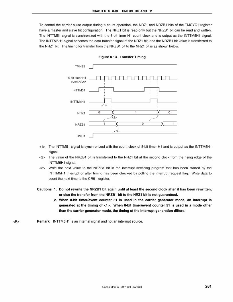
CHAPTER 8 8-BIT TIMERS H0 AND H1
User’s Manual U17336EJ5V0UD 261
To control the carrier pulse output during a count operation, the NRZ1 and NRZB1 bits of the TMCYC1 register
have a master and slave bit configuration. The NRZ1 bit is read-only but the NRZB1 bit can be read and written.
The INTTM51 signal is synchronized with the 8-bit timer H1 count clock and is output as the INTTM5H1 signal.
The INTTM5H1 signal becomes the data transfer signal of the NRZ1 bit, and the NRZB1 bit value is transferred to
the NRZ1 bit. The timing for transfer from the NRZB1 bit to the NRZ1 bit is as shown below.
Figure 8-13. Transfer Timing
8-bit timer H1count clock
TMHE1
INTTM51
INTTM5H1
NRZ1
NRZB1
RMC1
1
1
10
0 0
<1>
<2>
<3>
<1> The INTTM51 signal is synchronized with the count clock of 8-bit timer H1 and is output as the INTTM5H1
signal.
<2> The value of the NRZB1 bit is transferred to the NRZ1 bit at the second clock from the rising edge of the
INTTM5H1 signal.
<3> Write the next value to the NRZB1 bit in the interrupt servicing program that has been started by the
INTTM5H1 interrupt or after timing has been checked by polling the interrupt request flag. Write data to
count the next time to the CR51 register.
Cautions 1. Do not rewrite the NRZB1 bit again until at least the second clock after it has been rewritten,
or else the transfer from the NRZB1 bit to the NRZ1 bit is not guaranteed.
2. When 8-bit timer/event counter 51 is used in the carrier generator mode, an interrupt is
generated at the timing of <1>. When 8-bit timer/event counter 51 is used in a mode other
than the carrier generator mode, the timing of the interrupt generation differs.
Remark INTTM5H1 is an internal signal and not an interrupt source. <R>

CHAPTER 8 8-BIT TIMERS H0 AND H1
User’s Manual U17336EJ5V0UD 262
Setting
<1> Set each register.
Figure 8-14. Register Setting in Carrier Generator Mode
(i) Setting 8-bit timer H mode register 1 (TMHMD1)
0 0/1 0/1 0/1 0
Timer output enabled
Default setting of timer output level
Carrier generator mode selection
Count clock (fCNT) selection
Count operation stopped
1 0/1 1
TMMD10 TOLEV1 TOEN1CKS11CKS12TMHE1
TMHMD1
CKS10 TMMD11
(ii) CMP01 register setting
• Compare value
(iii) CMP11 register setting
• Compare value
(iv) TMCYC1 register setting
• RMC1 = 1 ... Remote control output enable bit
• NRZB1 = 0/1 ... carrier output enable bit
(v) TCL51 and TMC51 register setting
• See 7.3 Registers Controlling 8-bit Timer/Event Counters 50 and 51.
<2> When TMHE1 = 1, 8-bit timer H1 starts counting.
<3> When TCE51 of 8-bit timer mode control register 51 (TMC51) is set to 1, 8-bit timer/event counter 51 starts
counting.
<4> After the count operation is enabled, the first compare register to be compared is the CMP01 register.
When the count value of 8-bit timer counter H1 and the CMP01 register value match, the INTTMH1 signal
is generated, 8-bit timer counter H1 is cleared. At the same time, the compare register to be compared with
8-bit timer counter H1 is switched from the CMP01 register to the CMP11 register.
<5> When the count value of 8-bit timer counter H1 and the CMP11 register value match, the INTTMH1 signal
is generated, 8-bit timer counter H1 is cleared. At the same time, the compare register to be compared with
8-bit timer counter H1 is switched from the CMP11 register to the CMP01 register.
<6> By performing procedures <4> and <5> repeatedly, a carrier clock is generated.
<7> The INTTM51 signal is synchronized with count clock of 8-bit timer H1 and output as the INTTM5H1 signal.
The INTTM5H1 signal becomes the data transfer signal for the NRZB1 bit, and the NRZB1 bit value is
transferred to the NRZ1 bit.
<8> Write the next value to the NRZB1 bit in the interrupt servicing program that has been started by the
INTTM5H1 interrupt or after timing has been checked by polling the interrupt request flag. Write data to
count the next time to the CR51 register.
<9> When the NRZ1 bit is high level, a carrier clock is output by TOH1 output. <R>

CHAPTER 8 8-BIT TIMERS H0 AND H1
User’s Manual U17336EJ5V0UD 263
<10> By performing the procedures above, an arbitrary carrier clock is obtained. To stop the count operation,
clear TMHE1 to 0.
If the setting value of the CMP01 register is N, the setting value of the CMP11 register is M, and the count
clock frequency is fCNT, the carrier clock output cycle and duty are as follows.
• Carrier clock output cycle = (N + M + 2) / fCNT
• Duty = High-level width/carrier clock output width = (M + 1) / (N + M + 2)
Cautions 1. Be sure to set the CMP11 register when starting the timer count operation (TMHE1 = 1)
after the timer count operation was stopped (TMHE1 = 0) (be sure to set again even if
setting the same value to the CMP11 register).
2. Set so that the count clock frequency of TMH1 becomes more than 6 times the count
clock frequency of TM51.
3. Set the values of the CMP01 and CMP11 registers in a range of 01H to FFH.
4. The set value of the CMP11 register can be changed while the timer counter is
operating. However, it takes the duration of three operating clocks (signal selected by
the CKS12 to CKS10 bits of the TMHMD1 register) since the value of the CMP11
register has been changed until the value is transferred to the register.
5. Be sure to set the RMC1 bit before the count operation is started.
Remarks 1. For the setting of the output pin, see 8.3 (3) Port mode register 1 (PM1).
2. For how to enable the INTTMH1 signal interrupt, see CHAPTER 18 INTERRUPT
FUNCTIONS.

CHAPTER 8 8-BIT TIMERS H0 AND H1
User’s Manual U17336EJ5V0UD 264
Figure 8-15. Carrier Generator Mode Operation Timing (1/3)
(a) Operation when CMP01 = N, CMP11 = N
CMP01
CMP11
TMHE11
INTTMH1
Carrier clock
00H N 00H N 00H N 00H N 00H N 00H N
N
N
8-bit timer 51count clock
TM51 count value
CR51
TCE51
TOH1
0
0
1
1
0
0
1
1
0
0
INTTM51
NRZB1
NRZ1
Carrier clock
00H 01H K 00H 01H L 00H 01H M 00H 01H 00H 01HN
INTTM5H1
<1><2><3> <4>
<5>
<6>
<7>
8-bit timer H1count clock
8-bit timer counterH1 count value
K L M N
<1> When TMHE1 = 0 and TCE51 = 0, 8-bit timer counter H1 operation is stopped.
<2> When TMHE1 = 1 is set, 8-bit timer counter H1 starts a count operation. At that time, the carrier clock
remains default.
<3> When the count value of 8-bit timer counter H1 matches the CMP01 register value, the first INTTMH1 signal
is generated, the carrier clock signal is inverted, and the compare register to be compared with 8-bit timer
counter H1 is switched from the CMP01 register to the CMP11 register. 8-bit timer counter H1 is cleared to
00H.
<4> When the count value of 8-bit timer counter H1 matches the CMP11 register value, the INTTMH1 signal is
generated, the carrier clock signal is inverted, and the compare register to be compared with 8-bit timer
counter H1 is switched from the CMP11 register to the CMP01 register. 8-bit timer counter H1 is cleared to
00H. By performing procedures <3> and <4> repeatedly, a carrier clock with duty fixed to 50% is generated.
<5> When the INTTM51 signal is generated, it is synchronized with the 8-bit timer H1 count clock and is output as
the INTTM5H1 signal.
<6> The INTTM5H1 signal becomes the data transfer signal for the NRZB1 bit, and the NRZB1 bit value is
transferred to the NRZ1 bit.
<7> When NRZ1 = 0 is set, the TOH1 output becomes low level.
Remark INTTM5H1 is an internal signal and not an interrupt source. <R>

CHAPTER 8 8-BIT TIMERS H0 AND H1
User’s Manual U17336EJ5V0UD 265
Figure 8-15. Carrier Generator Mode Operation Timing (2/3)
(b) Operation when CMP01 = N, CMP11 = M
NCMP01
CMP11
TMHE1
INTTMH1
Carrier clock
TM51 count value
00H N 00H 01H M 00H N 00H 01H M 00H 00HN
M
TCE51
TOH1
0
0
1
1
0
0
1
1
0
0
INTTM51
NRZB1
NRZ1
Carrier clock
00H 01H K 00H 01H L 00H 01H M 00H 01H 00H 01HN
INTTM5H1
<1><2><3> <4>
<5>
<6><7>
8-bit timer 51count clock
8-bit timer H1count clock
8-bit timer counterH1 count value
KCR51 L M N
<1> When TMHE1 = 0 and TCE51 = 0, 8-bit timer counter H1 operation is stopped.
<2> When TMHE1 = 1 is set, 8-bit timer counter H1 starts a count operation. At that time, the carrier clock
remains default.
<3> When the count value of 8-bit timer counter H1 matches the CMP01 register value, the first INTTMH1 signal
is generated, the carrier clock signal is inverted, and the compare register to be compared with 8-bit timer
counter H1 is switched from the CMP01 register to the CMP11 register. 8-bit timer counter H1 is cleared to
00H.
<4> When the count value of 8-bit timer counter H1 matches the CMP11 register value, the INTTMH1 signal is
generated, the carrier clock signal is inverted, and the compare register to be compared with 8-bit timer
counter H1 is switched from the CMP11 register to the CMP01 register. 8-bit timer counter H1 is cleared to
00H. By performing procedures <3> and <4> repeatedly, a carrier clock with duty fixed to other than 50% is
generated.
<5> When the INTTM51 signal is generated, it is synchronized with the 8-bit timer H1 count clock and is output as
the INTTM5H1 signal.
<6> A carrier signal is output at the first rising edge of the carrier clock if NRZ1 is set to 1.
<7> When NRZ1 = 0, the TOH1 output is held at the high level and is not changed to low level while the carrier
clock is high level (from <6> and <7>, the high-level width of the carrier clock waveform is guaranteed).
Remark INTTM5H1 is an internal signal and not an interrupt source. <R>
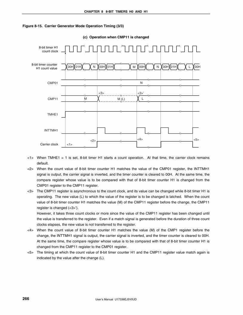
CHAPTER 8 8-BIT TIMERS H0 AND H1
User’s Manual U17336EJ5V0UD 266
Figure 8-15. Carrier Generator Mode Operation Timing (3/3)
(c) Operation when CMP11 is changed
8-bit timer H1
count clock
CMP01
TMHE1
INTTMH1
Carrier clock
00H 01H N 00H 01H 01HM 00H N 00H L 00H
<1>
<3>’
<4>
<3>
<2>
CMP11
<5>
M
N
LM (L)
8-bit timer counterH1 count value
<1> When TMHE1 = 1 is set, 8-bit timer H1 starts a count operation. At that time, the carrier clock remains
default.
<2> When the count value of 8-bit timer counter H1 matches the value of the CMP01 register, the INTTMH1
signal is output, the carrier signal is inverted, and the timer counter is cleared to 00H. At the same time, the
compare register whose value is to be compared with that of 8-bit timer counter H1 is changed from the
CMP01 register to the CMP11 register.
<3> The CMP11 register is asynchronous to the count clock, and its value can be changed while 8-bit timer H1 is
operating. The new value (L) to which the value of the register is to be changed is latched. When the count
value of 8-bit timer counter H1 matches the value (M) of the CMP11 register before the change, the CMP11
register is changed (<3>’).
However, it takes three count clocks or more since the value of the CMP11 register has been changed until
the value is transferred to the register. Even if a match signal is generated before the duration of three count
clocks elapses, the new value is not transferred to the register.
<4> When the count value of 8-bit timer counter H1 matches the value (M) of the CMP1 register before the
change, the INTTMH1 signal is output, the carrier signal is inverted, and the timer counter is cleared to 00H.
At the same time, the compare register whose value is to be compared with that of 8-bit timer counter H1 is
changed from the CMP11 register to the CMP01 register.
<5> The timing at which the count value of 8-bit timer counter H1 and the CMP11 register value match again is
indicated by the value after the change (L).

User’s Manual U17336EJ5V0UD 267
CHAPTER 9 WATCH TIMER
9.1 Functions of Watch Timer
The watch timer has the following functions.
• Watch timer
• Interval timer
The watch timer and the interval timer can be used simultaneously.
Figure 9-1 shows the watch timer block diagram.
Figure 9-1. Block Diagram of Watch Timer
fPRS/27
fW/24 fW/25 fW/26 fW/27 fW/28 fW/210 fW/211 fW/29fSUB
INTWT
INTWTI
WTM0WTM1WTM2WTM3WTM4WTM5WTM6WTM7
fW
Clear
11-bit prescalerClear
5-bit counter
Watch timer operation mode register (WTM)
Internal bus
Sel
ecto
r
Sel
ecto
r
Sel
ecto
r
Sel
ecto
r fWX/24
fWX/25fWX
Remark fPRS: Peripheral hardware clock frequency
fSUB: Subsystem clock frequency
fW: Watch timer clock frequency (fPRS/27 or fSUB)
fWX: fW or fW/29

CHAPTER 9 WATCH TIMER
User’s Manual U17336EJ5V0UD 268
(1) Watch timer
When the peripheral hardware clock or subsystem clock is used, interrupt request signals (INTWT) are
generated at preset intervals.
Table 9-1. Watch Timer Interrupt Time
Interrupt Time When Operated at
fSUB = 32.768 kHz
When Operated at
fPRS = 2 MHz
When Operated at
fPRS = 5 MHz
When Operated at
fPRS = 10 MHz
When Operated at
fPRS = 20 MHz
24/fW 488 μs 1.02 ms 410 μs 205 μs 102 μs
25/fW 977 μs 2.05 ms 819 μs 410 μs 205 μs
213/fW 0.25 s 0.52 s 0.210 s 0.105 s 52.5 ms
214/fW 0.5 s 1.05 s 0.419 s 0.210 s 0.105 s
Remark fPRS: Peripheral hardware clock frequency
fSUB: Subsystem clock frequency
fW: Watch timer clock frequency (fPRS/27 or fSUB)
(2) Interval timer
Interrupt request signals (INTWTI) are generated at preset time intervals.
Table 9-2. Interval Timer Interval Time
Interval Time When Operated at
fSUB = 32.768 kHz
When Operated at
fPRS = 2 MHz
When Operated at
fPRS = 5 MHz
When Operated at
fPRS = 10 MHz
When Operated at
fPRS = 20 MHz
24/fW 488 μs 1.02 ms 410 μs 205 μs 102 μs
25/fW 977 μs 2.05 ms 820 μs 410 μs 205 μs
26/fW 1.95 ms 4.10 ms 1.64 ms 820 μs 410 μs
27/fW 3.91 ms 8.20 ms 3.28 ms 1.64 ms 820 μs
28/fW 7.81 ms 16.4 ms 6.55 ms 3.28 ms 1.64 ms
29/fW 15.6 ms 32.8 ms 13.1 ms 6.55 ms 3.28 ms
210/fW 31.3 ms 65.5 ms 26.2 ms 13.1 ms 6.55 ms
211/fW 62.5 ms 131.1 ms 52.4 ms 26.2 ms 13.1 ms
Remark fPRS: Peripheral hardware clock frequency
fSUB: Subsystem clock frequency
fW: Watch timer clock frequency (fPRS/27 or fSUB)
9.2 Configuration of Watch Timer
The watch timer includes the following hardware.
Table 9-3. Watch Timer Configuration
Item Configuration
Counter 5 bits × 1
Prescaler 11 bits × 1
Control register Watch timer operation mode register (WTM)

CHAPTER 9 WATCH TIMER
User’s Manual U17336EJ5V0UD 269
9.3 Register Controlling Watch Timer
The watch timer is controlled by the watch timer operation mode register (WTM).
• Watch timer operation mode register (WTM)
This register sets the watch timer count clock, enables/disables operation, prescaler interval time, and 5-bit
counter operation control.
WTM is set by a 1-bit or 8-bit memory manipulation instruction.
Reset signal generation clears WTM to 00H.

CHAPTER 9 WATCH TIMER
User’s Manual U17336EJ5V0UD 270
Figure 9-2. Format of Watch Timer Operation Mode Register (WTM)
Address: FF6FH After reset: 00H R/W
Symbol 7 6 5 4 3 2 <1> <0>
WTM WTM7 WTM6 WTM5 WTM4 WTM3 WTM2 WTM1 WTM0
Watch timer count clock selection (fW)Note WTM7
fSUB = 32.768 kHz fPRS = 2 MHz fPRS = 5 MHz fPRS = 10 MHz fPRS = 20 MHz
0 fPRS/27 − 15.625 kHz 39.062 kHz 78.125 kHz 156.25 kHz
1 fSUB 32.768 kHz −
WTM6 WTM5 WTM4 Prescaler interval time selection
0 0 0 24/fW
0 0 1 25/fW
0 1 0 26/fW
0 1 1 27/fW
1 0 0 28/fW
1 0 1 29/fW
1 1 0 210/fW
1 1 1 211/fW
WTM3 WTM2 Selection of watch timer interrupt time
0 0 214/fW
0 1 213/fW
1 0 25/fW
1 1 24/fW
WTM1 5-bit counter operation control
0 Clear after operation stop
1 Start
WTM0 Watch timer operation enable
0 Operation stop (clear both prescaler and 5-bit counter)
1 Operation enable
Note If the peripheral hardware clock (fPRS) operates on the high-speed system clock (fXH) (XSEL = 1), the fPRS
operating frequency varies depending on the supply voltage.
• VDD = 4.0 to 5.5 V: fPRS ≤ 20 MHz
• VDD = 2.7 to 4.0 V: fPRS ≤ 10 MHz
• VDD = 1.8 to 2.7 V: fPRS ≤ 5 MHz (Standard and (A) grade products only)
Caution Do not change the count clock and interval time (by setting bits 4 to 7 (WTM4 to WTM7) of WTM)
during watch timer operation.
Remarks 1. fW: Watch timer clock frequency (fPRS/27 or fSUB)
2. fPRS: Peripheral hardware clock frequency
3. fSUB: Subsystem clock frequency
<R>

CHAPTER 9 WATCH TIMER
User’s Manual U17336EJ5V0UD 271
9.4 Watch Timer Operations
9.4.1 Watch timer operation
The watch timer generates an interrupt request signal (INTWT) at a specific time interval by using the peripheral
hardware clock or subsystem clock.
When bit 0 (WTM0) and bit 1 (WTM1) of the watch timer operation mode register (WTM) are set to 1, the count
operation starts. When these bits are cleared to 0, the 5-bit counter is cleared and the count operation stops.
When the interval timer is simultaneously operated, zero-second start can be achieved only for the watch timer by
clearing WTM1 to 0. In this case, however, the 11-bit prescaler is not cleared. Therefore, an error up to 29 × 1/fW
seconds occurs in the first overflow (INTWT) after zero-second start.
The interrupt request is generated at the following time intervals.
Table 9-4. Watch Timer Interrupt Time
WTM3 WTM2 Interrupt Time
Selection
When Operated at
fSUB = 32.768 kHz
(WTM7 = 1)
When Operated at
fPRS = 2 MHz
(WTM7 = 0)
When Operated at
fPRS = 5 MHz
(WTM7 = 0)
When Operated at
fPRS = 10 MHz
(WTM7 = 0)
When Operated at
fPRS = 20 MHz
(WTM7 = 0)
0 0 214/fW 0.5 s 1.05 s 0.419 s 0.210 s 0.105 s
0 1 213/fW 0.25 s 0.52 s 0.210 s 0.105 s 52.5 ms
1 0 25/fW 977 μs 2.05 ms 819 μs 410 μs 205 μs
1 1 24/fW 488 μs 1.02 ms 410 μs 205 μs 102 μs
Remarks 1. fW: Watch timer clock frequency (fPRS/27 or fSUB)
2. fPRS: Peripheral hardware clock frequency
3. fSUB: Subsystem clock frequency
9.4.2 Interval timer operation
The watch timer operates as interval timer which generates interrupt request signals (INTWTI) repeatedly at an
interval of the preset count value.
The interval time can be selected with bits 4 to 6 (WTM4 to WTM6) of the watch timer operation mode register
(WTM).
When bit 0 (WTM0) of the WTM is set to 1, the count operation starts. When this bit is set to 0, the count operation
stops.
Table 9-5. Interval Timer Interval Time
WTM6 WTM5 WTM4 Interval Time When Operated
at fSUB = 32.768
kHz (WTM7 = 1)
When Operated
at fPRS = 2 MHz
(WTM7 = 0)
When Operated
at fPRS = 5 MHz
(WTM7 = 0)
When Operated
at fPRS = 10 MHz
(WTM7 = 0)
When Operated
at fPRS = 20 MHz
(WTM7 = 0)
0 0 0 24/fW 488 μs 1.02 ms 410 μs 205 μs 102 μs
0 0 1 25/fW 977 μs 2.05 ms 820 μs 410 μs 205 μs
0 1 0 26/fW 1.95 ms 4.10 ms 1.64 ms 820 μs 410 μs
0 1 1 27/fW 3.91 ms 8.20 ms 3.28 ms 1.64 ms 820 μs
1 0 0 28/fW 7.81 ms 16.4 ms 6.55 ms 3.28 ms 1.64 ms
1 0 1 29/fW 15.6 ms 32.8 ms 13.1 ms 6.55 ms 3.28 ms
1 1 0 210/fW 31.3 ms 65.5 ms 26.2 ms 13.1 ms 6.55 ms
1 1 1 211/fW 62.5 ms 131.1 ms 52.4 ms 26.2 ms 13.1 ms
Remarks 1. fW: Watch timer clock frequency (fPRS/27 or fSUB)
2. fPRS: Peripheral hardware clock frequency
3. fSUB: Subsystem clock frequency

CHAPTER 9 WATCH TIMER
User’s Manual U17336EJ5V0UD 272
Figure 9-3. Operation Timing of Watch Timer/Interval Timer
0H
StartOverflow Overflow
5-bit counter
Count clock
Watch timerinterrupt INTWT
Interval timerinterrupt INTWTI
Interrupt time of watch timer (0.5 s)
Interval time(T)
T
Interrupt time of watch timer (0.5 s)
Remark fW: Watch timer clock frequency
Figures in parentheses are for operation with fW = 32.768 kHz (WTM7 = 1, WTM3, WTM2 = 0, 0)
9.5 Cautions for Watch Timer
When operation of the watch timer and 5-bit counter is enabled by the watch timer mode control register (WTM) (by
setting bits 0 (WTM0) and 1 (WTM1) of WTM to 1), the interval until the first interrupt request signal (INTWT) is
generated after the register is set does not exactly match the specification made with bits 2 and 3 (WTM2, WTM3) of
WTM. Subsequently, however, the INTWT signal is generated at the specified intervals.
Figure 9-4. Example of Generation of Watch Timer Interrupt Request Signal (INTWT)
(When Interrupt Period = 0.5 s)
It takes 0.515625 seconds for the first INTWT to be generated (29 × 1/32768 = 0.015625 s longer).
INTWT is then generated every 0.5 seconds.
0.5 s0.5 s0.515625 s
WTM0, WTM1
INTWT

User’s Manual U17336EJ5V0UD 273
CHAPTER 10 WATCHDOG TIMER
10.1 Functions of Watchdog Timer
The watchdog timer operates on the internal low-speed oscillation clock.
The watchdog timer is used to detect an inadvertent program loop. If a program loop is detected, an internal reset
signal is generated.
Program loop is detected in the following cases.
• If the watchdog timer counter overflows
• If a 1-bit manipulation instruction is executed on the watchdog timer enable register (WDTE)
• If data other than “ACH” is written to WDTE
• If data is written to WDTE during a window close period
• If the instruction is fetched from an area not set by the IMS and IXS registers (detection of an invalid check while
the CPU hangs up)
• If the CPU accesses an area that is not set by the IMS and IXS registers (excluding FB00H to FFFFH) by
executing a read/write instruction (detection of an abnormal access during a CPU program loop)
When a reset occurs due to the watchdog timer, bit 4 (WDTRF) of the reset control flag register (RESF) is set to 1.
For details of RESF, see CHAPTER 21 RESET FUNCTION.

CHAPTER 10 WATCHDOG TIMER
User’s Manual U17336EJ5V0UD 274
10.2 Configuration of Watchdog Timer
The watchdog timer includes the following hardware.
Table 10-1. Configuration of Watchdog Timer
Item Configuration
Control register Watchdog timer enable register (WDTE)
How the counter operation is controlled, overflow time, and window open period are set by the option byte.
Table 10-2. Setting of Option Bytes and Watchdog Timer
Setting of Watchdog Timer Option Byte (0080H)
Window open period Bits 6 and 5 (WINDOW1, WINDOW0)
Controlling counter operation of watchdog timer Bit 4 (WDTON)
Overflow time of watchdog timer Bits 3 to 1 (WDCS2 to WDCS0)
Remark For the option byte, see CHAPTER 24 OPTION BYTE.
Figure 10-1. Block Diagram of Watchdog Timer
fRL/2Clock input
controller
Resetoutput
controllerInternal reset signal
Internal bus
Selector17-bitcounter
210/fRL to217/fRL
Watchdog timer enableregister (WDTE)
Clear, reset control
WDTON of option byte (0080H)
WINDOW1 and WINDOW0of option byte (0080H)
Count clearsignal
WDCS2 to WDCS0 of option byte (0080H)
Overflow signal
CPU access signal CPU accesserror detector
Window size determination
signal
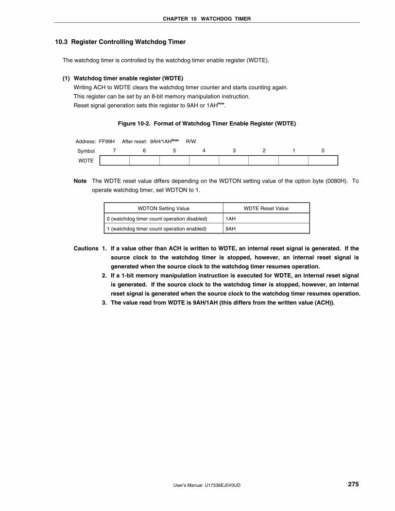
CHAPTER 10 WATCHDOG TIMER
User’s Manual U17336EJ5V0UD 275
10.3 Register Controlling Watchdog Timer
The watchdog timer is controlled by the watchdog timer enable register (WDTE).
(1) Watchdog timer enable register (WDTE)
Writing ACH to WDTE clears the watchdog timer counter and starts counting again.
This register can be set by an 8-bit memory manipulation instruction.
Reset signal generation sets this register to 9AH or 1AHNote.
Figure 10-2. Format of Watchdog Timer Enable Register (WDTE)
01234567Symbol
WDTE
Address: FF99H After reset: 9AH/1AHNote R/W
Note The WDTE reset value differs depending on the WDTON setting value of the option byte (0080H). To
operate watchdog timer, set WDTON to 1.
WDTON Setting Value WDTE Reset Value
0 (watchdog timer count operation disabled) 1AH
1 (watchdog timer count operation enabled) 9AH
Cautions 1. If a value other than ACH is written to WDTE, an internal reset signal is generated. If the
source clock to the watchdog timer is stopped, however, an internal reset signal is
generated when the source clock to the watchdog timer resumes operation.
2. If a 1-bit memory manipulation instruction is executed for WDTE, an internal reset signal
is generated. If the source clock to the watchdog timer is stopped, however, an internal
reset signal is generated when the source clock to the watchdog timer resumes operation.
3. The value read from WDTE is 9AH/1AH (this differs from the written value (ACH)).

CHAPTER 10 WATCHDOG TIMER
User’s Manual U17336EJ5V0UD 276
10.4 Operation of Watchdog Timer
10.4.1 Controlling operation of watchdog timer
1. When the watchdog timer is used, its operation is specified by the option byte (0080H).
• Enable counting operation of the watchdog timer by setting bit 4 (WDTON) of the option byte (0080H) to 1
(the counter starts operating after a reset release) (for details, see CHAPTER 26).
WDTON Operation Control of Watchdog Timer Counter/Illegal Access Detection
0 Counter operation disabled (counting stopped after reset), illegal access detection operation disabled
1 Counter operation enabled (counting started after reset), illegal access detection operation enabled
• Set an overflow time by using bits 3 to 1 (WDCS2 to WDCS0) of the option byte (0080H) (for details, see
10.4.2 and CHAPTER 24).
• Set a window open period by using bits 6 and 5 (WINDOW1 and WINDOW0) of the option byte (0080H) (for
details, see 10.4.3 and CHAPTER 24).
2. After a reset release, the watchdog timer starts counting.
3. By writing “ACH” to WDTE after the watchdog timer starts counting and before the overflow time set by the
option byte, the watchdog timer is cleared and starts counting again.
4. After that, write WDTE the second time or later after a reset release during the window open period. If WDTE
is written during a window close period, an internal reset signal is generated.
5. If the overflow time expires without “ACH” written to WDTE, an internal reset signal is generated.
A internal reset signal is generated in the following cases.
• If a 1-bit manipulation instruction is executed on the watchdog timer enable register (WDTE)
• If data other than “ACH” is written to WDTE
• If the instruction is fetched from an area not set by the IMS and IXS registers (detection of an invalid check
during a CPU program loop)
• If the CPU accesses an area not set by the IMS and IXS registers (excluding FB00H to FFFFH) by executing
a read/write instruction (detection of an abnormal access during a CPU program loop)
Cautions 1. The first writing to WDTE after a reset release clears the watchdog timer, if it is made before
the overflow time regardless of the timing of the writing, and the watchdog timer starts
counting again.
2. If the watchdog timer is cleared by writing “ACH” to WDTE, the actual overflow time may be
different from the overflow time set by the option byte by up to 2/fRL seconds.
3. The watchdog timer can be cleared immediately before the count value overflows (FFFFH).

CHAPTER 10 WATCHDOG TIMER
User’s Manual U17336EJ5V0UD 277
Cautions 4. The operation of the watchdog timer in the HALT and STOP modes differs as follows
depending on the set value of bit 0 (LSROSC) of the option byte.
LSROSC = 0 (Internal Low-Speed
Oscillator Can Be Stopped by Software)
LSROSC = 1 (Internal Low-Speed
Oscillator Cannot Be Stopped)
In HALT mode
In STOP mode
Watchdog timer operation stops. Watchdog timer operation continues.
If LSROSC = 0, the watchdog timer resumes counting after the HALT or STOP mode is
released. At this time, the counter is not cleared to 0 but starts counting from the value at
which it was stopped.
If oscillation of the internal low-speed oscillator is stopped by setting LSRSTOP (bit 1 of the
internal oscillation mode register (RCM) = 1) when LSROSC = 0, the watchdog timer stops
operating. At this time, the counter is not cleared to 0.
5. The watchdog timer continues its operation during self programming and EEPROM emulation
of the flash memory. During processing, the interrupt acknowledge time is delayed. Set the
overflow time and window size taking this delay into consideration.
10.4.2 Setting overflow time of watchdog timer
Set the overflow time of the watchdog timer by using bits 3 to 1 (WDCS2 to WDCS0) of the option byte (0080H).
If an overflow occurs, an internal reset signal is generated. The present count is cleared and the watchdog timer
starts counting again by writing “ACH” to WDTE during the window open period before the overflow time.
The following overflow time is set.
Table 10-3. Setting of Overflow Time of Watchdog Timer
WDCS2 WDCS1 WDCS0 Overflow Time of Watchdog Timer
0 0 0 210/fRL (3.88 ms)
0 0 1 211/fRL (7.76 ms)
0 1 0 212/fRL (15.52 ms)
0 1 1 213/fRL (31.03 ms)
1 0 0 214/fRL (62.06 ms)
1 0 1 215/fRL (124.12 ms)
1 1 0 216/fRL (248.24 ms)
1 1 1 217/fRL (496.48 ms)
Cautions 1. The combination of WDCS2 = WDCS1 = WDCS0 = 0 and WINDOW1 = WINDOW0 = 0
is prohibited.
2. The watchdog timer continues its operation during self programming and EEPROM
emulation of the flash memory. During processing, the interrupt acknowledge time
is delayed. Set the overflow time and window size taking this delay into
consideration.
Remarks 1. fRL: Internal low-speed oscillation clock frequency
2. ( ): fRL = 264 kHz (MAX.)
<R>
<R>

CHAPTER 10 WATCHDOG TIMER
User’s Manual U17336EJ5V0UD 278
10.4.3 Setting window open period of watchdog timer
Set the window open period of the watchdog timer by using bits 6 and 5 (WINDOW1, WINDOW0) of the option
byte (0080H). The outline of the window is as follows.
• If “ACH” is written to WDTE during the window open period, the watchdog timer is cleared and starts counting
again.
• Even if “ACH” is written to WDTE during the window close period, an abnormality is detected and an internal
reset signal is generated.
Example: If the window open period is 25%
Window close period (75%)Window openperiod (25%)
Countingstarts
Overflowtime
Counting starts again when ACH is written to WDTE.
Internal reset signal is generated if ACH is written to WDTE.
Caution The first writing to WDTE after a reset release clears the watchdog timer, if it is made before the
overflow time regardless of the timing of the writing, and the watchdog timer starts counting
again.
The window open period to be set is as follows.
Table 10-4. Setting Window Open Period of Watchdog Timer
WINDOW1 WINDOW0 Window Open Period of Watchdog Timer
0 0 25%
0 1 50%
1 0 75%
1 1 100%
Cautions 1. The combination of WDCS2 = WDCS1 = WDCS0 = 0 and WINDOW1 = WINDOW0 = 0
is prohibited.
2. The watchdog timer continues its operation during self programming and EEPROM
emulation of the flash memory. During processing, the interrupt acknowledge time
is delayed. Set the overflow time and window size taking this delay into
consideration.
<R>
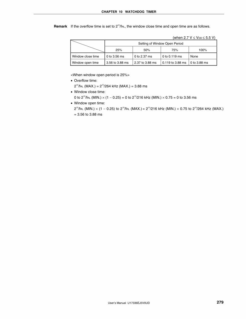
CHAPTER 10 WATCHDOG TIMER
User’s Manual U17336EJ5V0UD 279
Remark If the overflow time is set to 210/fRL, the window close time and open time are as follows.
(when 2.7 V ≤ VDD ≤ 5.5 V)
Setting of Window Open Period
25% 50% 75% 100%
Window close time 0 to 3.56 ms 0 to 2.37 ms 0 to 0.119 ms None
Window open time 3.56 to 3.88 ms 2.37 to 3.88 ms 0.119 to 3.88 ms 0 to 3.88 ms
<When window open period is 25%>
• Overflow time:
210/fRL (MAX.) = 210/264 kHz (MAX.) = 3.88 ms
• Window close time:
0 to 210/fRL (MIN.) × (1 − 0.25) = 0 to 210/216 kHz (MIN.) × 0.75 = 0 to 3.56 ms
• Window open time:
210/fRL (MIN.) × (1 − 0.25) to 210/fRL (MAX.) = 210/216 kHz (MIN.) × 0.75 to 210/264 kHz (MAX.)
= 3.56 to 3.88 ms

User’s Manual U17336EJ5V0UD 280
CHAPTER 11 CLOCK OUTPUT CONTROLLER (48-PIN PRODUCTS ONLY)
11.1 Functions of Clock Output Controller
The clock output controller is intended for carrier output during remote controlled transmission and clock output for
supply to peripheral ICs. The clock selected with the clock output selection register (CKS) is output.
Figure 11-1 shows the block diagram of clock output controller.
Figure 11-1. Block Diagram of Clock Output Controller
fPRS
fPRS to fPRS/27
fSUB
CLOE
8
PCL/INTP6/P140Clock
controller
Prescaler
Internal bus
CCS3
Clock output select register (CKS)
CCS2 CCS1 CCS0
Output latch(P140)
PM140
Sel
ecto
r

CHAPTER 11 CLOCK OUTPUT CONTROLLER (48-PIN PRODUCTS ONLY)
User’s Manual U17336EJ5V0UD 281
11.2 Configuration of Clock Output Controller
The clock output controller includes the following hardware.
Table 11-1. Configuration of Clock Output Controller
Item Configuration
Control registers Clock output selection register (CKS)
Port mode register 14 (PM14)
Port register 14 (P14)
11.3 Registers Controlling Clock Output Controller
The following two registers are used to control the clock output controller.
• Clock output selection register (CKS)
• Port mode register 14 (PM14)
(1) Clock output selection register (CKS)
This register sets output enable/disable for clock output (PCL), and sets the output clock.
CKS is set by a 1-bit or 8-bit memory manipulation instruction.
Reset signal generation sets CKS to 00H.

CHAPTER 11 CLOCK OUTPUT CONTROLLER (48-PIN PRODUCTS ONLY)
User’s Manual U17336EJ5V0UD 282
Figure 11-2. Format of Clock Output Selection Register (CKS)
Address: FF40H After reset: 00H R/W
Symbol 7 6 5 <4> 3 2 1 0
CKS 0 0 0 CLOE CCS3 CCS2 CCS1 CCS0
CLOE PCL output enable/disable specification
0 Clock division circuit operation stopped. PCL fixed to low level.
1 Clock division circuit operation enabled. PCL output enabled.
PCL output clock selectionNote 1 CCS3 CCS2 CCS1 CCS0
fSUB =
32.768 kHz
fPRS =
10 MHz
fPRS =
20 MHz
0 0 0 0 fPRSNote 2 10 MHz Setting
prohibitedNote 3
0 0 0 1 fPRS/2 5 MHz 10 MHz
0 0 1 0 fPRS/22 2.5 MHz 5 MHz
0 0 1 1 fPRS/23 1.25 MHz 2.5 MHz
0 1 0 0 fPRS/24 625 kHz 1.25 MHz
0 1 0 1 fPRS/25 312.5 kHz 625 kHz
0 1 1 0 fPRS/26 156.25 kHz 312.5 kHz
0 1 1 1 fPRS/27
−
78.125 kHz 156.25 kHz
1 0 0 0 fSUB 32.768 kHz −
Other than above Setting prohibited
Notes 1. If the peripheral hardware clock (fPRS) operates on the high-speed system clock (fXH) (XSEL = 1), the
fPRS operating frequency varies depending on the supply voltage.
• VDD = 4.0 to 5.5 V: fPRS ≤ 20 MHz
• VDD = 2.7 to 4.0 V: fPRS ≤ 10 MHz
• VDD = 1.8 to 2.7 V: fPRS ≤ 5 MHz (Standard and (A) grade products only)
2. If the peripheral hardware clock (fPRS) operates on the internal high-speed oscillation clock (XSEL = 0)
when 1.8 V ≤ VDD < 2.7 V, setting CCS3 = CCS2 = CCS1 = CCS0 = 0 (output clock of PCL: fPRS) is
prohibited.
3. The PCL output clock prohibits settings if they exceed 10 MHz.
Caution Set CCS3 to CCS0 while the clock output operation is stopped (CLOE = 0).
Remarks 1. fPRS: Peripheral hardware clock frequency
2. fSUB: Subsystem clock frequency
<R>
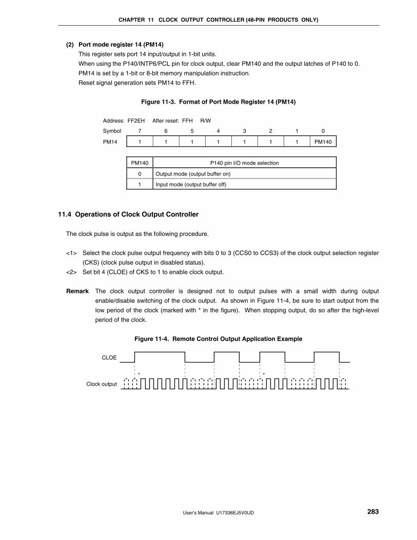
CHAPTER 11 CLOCK OUTPUT CONTROLLER (48-PIN PRODUCTS ONLY)
User’s Manual U17336EJ5V0UD 283
(2) Port mode register 14 (PM14)
This register sets port 14 input/output in 1-bit units.
When using the P140/INTP6/PCL pin for clock output, clear PM140 and the output latches of P140 to 0.
PM14 is set by a 1-bit or 8-bit memory manipulation instruction.
Reset signal generation sets PM14 to FFH.
Figure 11-3. Format of Port Mode Register 14 (PM14)
Address: FF2EH After reset: FFH R/W
Symbol 7 6 5 4 3 2 1 0
PM14 1 1 1 1 1 1 1 PM140
PM140 P140 pin I/O mode selection
0 Output mode (output buffer on)
1 Input mode (output buffer off)
11.4 Operations of Clock Output Controller
The clock pulse is output as the following procedure.
<1> Select the clock pulse output frequency with bits 0 to 3 (CCS0 to CCS3) of the clock output selection register
(CKS) (clock pulse output in disabled status).
<2> Set bit 4 (CLOE) of CKS to 1 to enable clock output.
Remark The clock output controller is designed not to output pulses with a small width during output
enable/disable switching of the clock output. As shown in Figure 11-4, be sure to start output from the
low period of the clock (marked with * in the figure). When stopping output, do so after the high-level
period of the clock.
Figure 11-4. Remote Control Output Application Example
CLOE
Clock output
* *

User’s Manual U17336EJ5V0UD 284
CHAPTER 12 A/D CONVERTER
12.1 Function of A/D Converter
The A/D converter converts an analog input signal into a digital value, and consists of up to eight channels (ANI0 to
ANI7Note) with a resolution of 10 bits.
The A/D converter has the following function.
• 10-bit resolution A/D conversion
10-bit resolution A/D conversion is carried out repeatedly for one analog input channel selected from ANI0 to
ANI7Note. Each time an A/D conversion operation ends, an interrupt request (INTAD) is generated.
Note 38-pin products: ANI0 to ANI5
44-pin and 48-pin products: ANI0 to ANI7
Figure 12-1. Block Diagram of A/D Converter
AVREF
AVSS
INTAD
ADCS bit
ADCS FR2 FR1 ADCEFR0
Sample & hold circuit
AVSS
Voltage comparator
A/D converter mode register (ADM)
Internal bus
3
ADS2 ADS1 ADS0
Analog input channelspecification register (ADS)
ANI0/P20ANI1/P21ANI2/P22ANI3/P23ANI4/P24ANI5/P25
ANI6/P26Note
ANI7/P27Note
Controller
A/D conversion resultregister (ADCR)
Successive approximation register (SAR)
LV1 LV0
5
A/D port configuration register (ADPC)
ADPC3 ADPC2 ADPC1 ADPC0
4
Sel
ecto
r
Tap
sel
ecto
r
Note 44-pin and 48-pin products only
<R>
<R>

CHAPTER 12 A/D CONVERTER
User’s Manual U17336EJ5V0UD 285
12.2 Configuration of A/D Converter
The A/D converter includes the following hardware.
(1) ANI0 to ANI7 pinsNote
These are the analog input pins of the 8-channel A/D converter. They input analog signals to be converted into
digital signals. Pins other than the one selected as the analog input pin can be used as I/O port pins.
Note 38-pin products: ANI0 to ANI5 pins
44-pin and 48-pin products: ANI0 to ANI7 pins
(2) Sample & hold circuit
The sample & hold circuit samples the input voltage of the analog input pin selected by the selector when A/D
conversion is started, and holds the sampled voltage value during A/D conversion.
(3) Series resistor string
The series resistor string is connected between AVREF and AVSS, and generates a voltage to be compared with
the sampled voltage value.
Figure 12-2. Circuit Configuration of Series Resistor String
ADCS
Series resistor string
AVREF
P-ch
AVSS
(4) Voltage comparator
The voltage comparator compares the sampled voltage value and the output voltage of the series resistor string.
(5) Successive approximation register (SAR)
This register converts the result of comparison by the voltage comparator, starting from the most significant bit
(MSB).
When the voltage value is converted into a digital value down to the least significant bit (LSB) (end of A/D
conversion), the contents of the SAR register are transferred to the A/D conversion result register (ADCR).
(6) 10-bit A/D conversion result register (ADCR)
The A/D conversion result is loaded from the successive approximation register to this register each time A/D
conversion is completed, and the ADCR register holds the A/D conversion result in its higher 10 bits (the lower 6
bits are fixed to 0).
<R>

CHAPTER 12 A/D CONVERTER
User’s Manual U17336EJ5V0UD 286
(7) 8-bit A/D conversion result register (ADCRH)
The A/D conversion result is loaded from the successive approximation register to this register each time A/D
conversion is completed, and the ADCRH register stores the higher 8 bits of the A/D conversion result.
Caution When data is read from ADCR and ADCRH, a wait cycle is generated. Do not read data from
ADCR and ADCRH when the CPU is operating on the subsystem clock and the peripheral
hardware clock is stopped. For details, see CHAPTER 34 CAUTIONS FOR WAIT.
(8) Controller
This circuit controls the conversion time of an input analog signal that is to be converted into a digital signal, as
well as starting and stopping of the conversion operation. When A/D conversion has been completed, this
controller generates INTAD.
(9) AVREF pin
This pin inputs an analog power/reference voltage to the A/D converter. Make this pin the same potential as the
VDD pin when port 2 is used as a digital port.
The signal input to the ANI0 to ANI7 pinsNote is converted into a digital signal, based on the voltage applied across
AVREF and AVSS.
(10) AVSS pin
This is the ground potential pin of the A/D converter. Always use this pin at the same potential as that of the VSS
pin even when the A/D converter is not used.
(11) A/D converter mode register (ADM)
This register is used to set the conversion time of the analog input signal to be converted, and to start or stop the
conversion operation.
(12) A/D port configuration register (ADPC)
This register switches the ANI0/P20 to ANI7/P27 pinsNote to analog input of A/D converter or digital I/O of port.
(13) Analog input channel specification register (ADS)
This register is used to specify the port that inputs the analog voltage to be converted into a digital signal.
(14) Port mode register 2 (PM2)
This register switches the ANI0/P20 to ANI7/P27 pinsNote to input or output.
Note 38-pin products: ANI0 to ANI5 pins
44-pin and 48-pin products: ANI0 to ANI7 pins
<R>
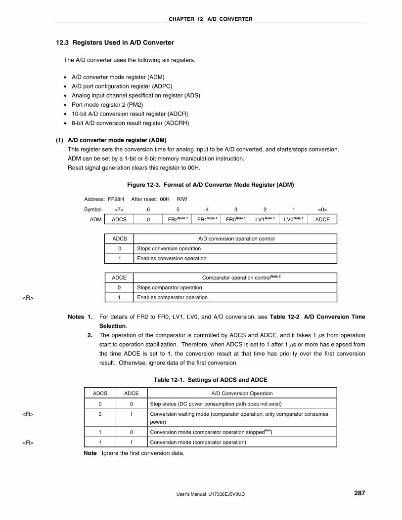
CHAPTER 12 A/D CONVERTER
User’s Manual U17336EJ5V0UD 287
12.3 Registers Used in A/D Converter
The A/D converter uses the following six registers.
• A/D converter mode register (ADM)
• A/D port configuration register (ADPC)
• Analog input channel specification register (ADS)
• Port mode register 2 (PM2)
• 10-bit A/D conversion result register (ADCR)
• 8-bit A/D conversion result register (ADCRH)
(1) A/D converter mode register (ADM)
This register sets the conversion time for analog input to be A/D converted, and starts/stops conversion.
ADM can be set by a 1-bit or 8-bit memory manipulation instruction.
Reset signal generation clears this register to 00H.
Figure 12-3. Format of A/D Converter Mode Register (ADM)
ADCELV0Note 1LV1Note 1FR0Note 1FR1Note 1FR2Note 10ADCS
A/D conversion operation control
Stops conversion operation
Enables conversion operation
ADCS
0
1
<0>123456<7>
ADM
Address: FF28H After reset: 00H R/W
Symbol
Comparator operation controlNote 2
Stops comparator operation
Enables comparator operation
ADCE
0
1
Notes 1. For details of FR2 to FR0, LV1, LV0, and A/D conversion, see Table 12-2 A/D Conversion Time
Selection.
2. The operation of the comparator is controlled by ADCS and ADCE, and it takes 1 μs from operation
start to operation stabilization. Therefore, when ADCS is set to 1 after 1 μs or more has elapsed from
the time ADCE is set to 1, the conversion result at that time has priority over the first conversion
result. Otherwise, ignore data of the first conversion.
Table 12-1. Settings of ADCS and ADCE
ADCS ADCE A/D Conversion Operation
0 0 Stop status (DC power consumption path does not exist)
0 1 Conversion waiting mode (comparator operation, only comparator consumes
power)
1 0 Conversion mode (comparator operation stoppedNote)
1 1 Conversion mode (comparator operation)
Note Ignore the first conversion data.
<R>
<R>
<R>
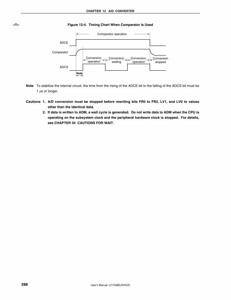
CHAPTER 12 A/D CONVERTER
User’s Manual U17336EJ5V0UD 288
Figure 12-4. Timing Chart When Comparator Is Used
ADCE
Comparator
ADCS
Conversion operation
Conversion operation
Conversionstopped
Conversionwaiting
Comparator operation
Note
Note To stabilize the internal circuit, the time from the rising of the ADCE bit to the falling of the ADCS bit must be
1 μs or longer.
Cautions 1. A/D conversion must be stopped before rewriting bits FR0 to FR2, LV1, and LV0 to values
other than the identical data.
2. If data is written to ADM, a wait cycle is generated. Do not write data to ADM when the CPU is
operating on the subsystem clock and the peripheral hardware clock is stopped. For details,
see CHAPTER 34 CAUTIONS FOR WAIT.
<R>

CHAPTER 12 A/D CONVERTER
User’s Manual U17336EJ5V0UD 289
Table 12-2. A/D Conversion Time Selection
(1) 2.7 V ≤ AVREF ≤ 5.5 V
A/D Converter Mode Register (ADM) Conversion Time Selection
FR2 FR1 FR0 LV1 LV0 fPRS = 2 MHz fPRS = 10 MHz fPRS = 20 MHzNote
Conversion Clock
(fAD)
0 0 0 0 0 264/fPRS 26.4 μs 13.2 μsNote fPRS/12
0 0 1 0 0 176/fPRS 17.6 μs 8.8 μsNote fPRS/8
0 1 0 0 0 132/fPRS 13.2 μs 6.6 μsNote fPRS/6
0 1 1 0 0 88/fPRS
Setting prohibited
8.8 μsNote fPRS/4
1 0 0 0 0 66/fPRS 33.0 μs 6.6 μsNote fPRS/3
1 0 1 0 0 44/fPRS 22.0 μs Setting prohibited
Setting prohibited
fPRS/2
Other than above Setting prohibited
Note This can be set only when 4.0 V ≤ AVREF ≤ 5.5 V.
(2) 2.3 V ≤ AVREF < 2.7 V
A/D Converter Mode Register (ADM) Conversion Time Selection
FR2 FR1 FR0 LV1 LV0 fPRS = 2 MHz fPRS = 5 MHz
Conversion Clock
(fAD)
0 0 0 0 1 480/fPRS Setting prohibited fPRS/12
0 0 1 0 1 320/fPRS 64.0 μs fPRS/8
0 1 0 0 1 240/fPRS 48.0 μs fPRS/6
0 1 1 0 1 160/fPRS
Setting prohibited
32.0 μs fPRS/4
1 0 0 0 1 120/fPRS 60.0 μs Setting prohibited fPRS/3
1 0 1 0 1 80/fPRS 40.0 μs Setting prohibited fPRS/2
Other than above Setting prohibited
Cautions 1. Set the conversion times with the following conditions.
• 4.0 V ≤ AVREF ≤ 5.5 V: fAD = 0.6 to 3.6 MHz
• 2.7 V ≤ AVREF < 4.0 V: fAD = 0.6 to 1.8 MHz
• 2.3 V ≤ AVREF < 2.7 V: fAD = 0.6 to 1.48 MHz
2. When rewriting FR2 to FR0, LV1, and LV0 to other than the same data, stop A/D conversion
once (ADCS = 0) beforehand.
3. Change LV1 and LV0 from the default value, when 2.3 V ≤ AVREF < 2.7 V.
4. The above conversion time does not include clock frequency errors. Select conversion time,
taking clock frequency errors into consideration.
Remark fPRS: Peripheral hardware clock frequency

CHAPTER 12 A/D CONVERTER
User’s Manual U17336EJ5V0UD 290
Figure 12-5. A/D Converter Sampling and A/D Conversion Timing
ADCS
WaitperiodNote
Conversion time Conversion time
Sampling
Samplingtiming
INTAD
ADCS ← 1 or ADS rewrite
SamplingSARclear
SARclear
Transferto ADCR,
INTADgeneration
Successive conversion
Note For details of wait period, see CHAPTER 34 CAUTIONS FOR WAIT.
(2) 10-bit A/D conversion result register (ADCR)
This register is a 16-bit register that stores the A/D conversion result. The lower 6 bits are fixed to 0. Each time
A/D conversion ends, the conversion result is loaded from the successive approximation register. The higher 8
bits of the conversion result are stored in FF09H and the lower 2 bits are stored in the higher 2 bits of FF08H.
ADCR can be read by a 16-bit memory manipulation instruction.
Reset signal generation clears this register to 0000H.
Figure 12-6. Format of 10-bit A/D Conversion Result Register (ADCR)
Symbol
Address: FF08H, FF09H After reset: 0000H R
FF09H FF08H
000000ADCR
Cautions 1. When writing to the A/D converter mode register (ADM), analog input channel specification
register (ADS), and A/D port configuration register (ADPC), the contents of ADCR may
become undefined. Read the conversion result following conversion completion before
writing to ADM, ADS, and ADPC. Using timing other than the above may cause an incorrect
conversion result to be read.
2. If data is read from ADCR, a wait cycle is generated. Do not read data from ADCR when the
CPU is operating on the subsystem clock and the peripheral hardware clock is stopped. For
details, see CHAPTER 34 CAUTIONS FOR WAIT.

CHAPTER 12 A/D CONVERTER
User’s Manual U17336EJ5V0UD 291
(3) 8-bit A/D conversion result register (ADCRH)
This register is an 8-bit register that stores the A/D conversion result. The higher 8 bits of 10-bit resolution are
stored.
ADCRH can be read by an 8-bit memory manipulation instruction.
Reset signal generation clears this register to 00H.
Figure 12-7. Format of 8-bit A/D Conversion Result Register (ADCRH)
Symbol
ADCRH
Address: FF09H After reset: 00H R
7 6 5 4 3 2 1 0
Cautions 1. When writing to the A/D converter mode register (ADM), analog input channel specification
register (ADS), and A/D port configuration register (ADPC), the contents of ADCRH may
become undefined. Read the conversion result following conversion completion before
writing to ADM, ADS, and ADPC. Using timing other than the above may cause an incorrect
conversion result to be read.
2. If data is read from ADCRH, a wait cycle is generated. Do not read data from ADCRH when
the CPU is operating on the subsystem clock and the peripheral hardware clock is stopped.
For details, see CHAPTER 34 CAUTIONS FOR WAIT.
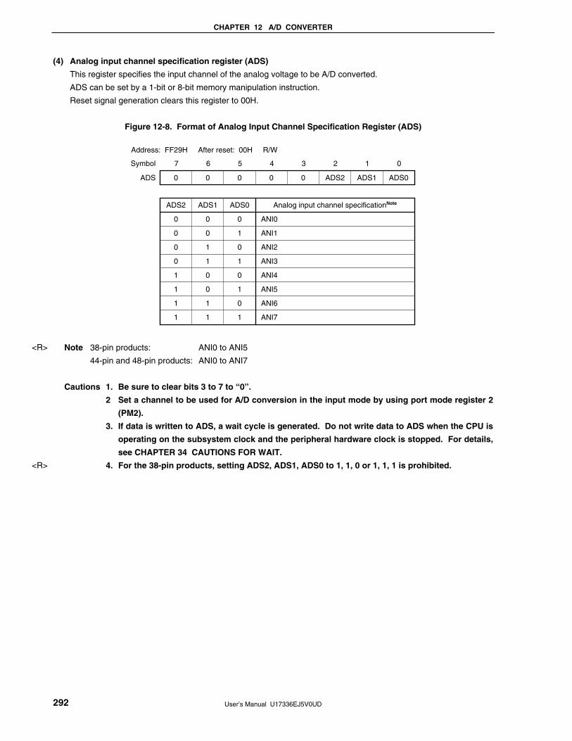
CHAPTER 12 A/D CONVERTER
User’s Manual U17336EJ5V0UD 292
(4) Analog input channel specification register (ADS)
This register specifies the input channel of the analog voltage to be A/D converted.
ADS can be set by a 1-bit or 8-bit memory manipulation instruction.
Reset signal generation clears this register to 00H.
Figure 12-8. Format of Analog Input Channel Specification Register (ADS)
ADS0ADS1ADS200000
Analog input channel specificationNote
ANI0
ANI1
ANI2
ANI3
ANI4
ANI5
ANI6
ANI7
ADS0
0
1
0
1
0
1
0
1
ADS1
0
0
1
1
0
0
1
1
ADS2
0
0
0
0
1
1
1
1
01234567
ADS
Address: FF29H After reset: 00H R/W
Symbol
Note 38-pin products: ANI0 to ANI5
44-pin and 48-pin products: ANI0 to ANI7
Cautions 1. Be sure to clear bits 3 to 7 to “0”.
2 Set a channel to be used for A/D conversion in the input mode by using port mode register 2
(PM2).
3. If data is written to ADS, a wait cycle is generated. Do not write data to ADS when the CPU is
operating on the subsystem clock and the peripheral hardware clock is stopped. For details,
see CHAPTER 34 CAUTIONS FOR WAIT.
4. For the 38-pin products, setting ADS2, ADS1, ADS0 to 1, 1, 0 or 1, 1, 1 is prohibited.
<R>
<R>

CHAPTER 12 A/D CONVERTER
User’s Manual U17336EJ5V0UD 293
(5) A/D port configuration register (ADPC)
This register switches the ANI0/P20 to ANI7/P27 pinsNote to analog input of A/D converter or digital I/O of port.
ADPC can be set by a 1-bit or 8-bit memory manipulation instruction.
Reset signal generation clears this register to 00H.
Note 38-pin products: ANI0/P20 to ANI5/P25 pins
44-pin and 48-pin products ANI0/P20 to ANI7/P27 pins
Figure 12-9. Format of A/D Port Configuration Register (ADPC)
ADPC0ADPC1ADPC2ADPC30000
Analog input (A)/digital I/O (D) switching
Setting prohibited
ADPC3
01234567
ADPC
Address: FF2FH After reset: 00H R/W
Symbol
ANI7/P27
A
A
A
A
A
A
A
A
D
ANI6/P26
A
A
A
A
A
A
A
D
D
ANI5/P25
A
A
A
A
A
A
D
D
D
ANI4/P24
A
A
A
A
A
D
D
D
D
ANI3/P23
A
A
A
A
D
D
D
D
D
ANI2/P22
A
A
A
D
D
D
D
D
D
ANI1/P21
A
A
D
D
D
D
D
D
D
ANI0/P20
A
D
D
D
D
D
D
D
D
0
0
0
0
0
0
0
0
1
ADPC2
0
0
0
0
1
1
1
1
0
ADPC1
0
0
1
1
0
0
1
1
0
ADPC0
0
1
0
1
0
1
0
1
0
Other than above
Cautions 1. Set a channel to be used for A/D conversion in the input mode by using port mode register 2
(PM2).
2. If data is written to ADPC, a wait cycle is generated. Do not write data to ADPC when the CPU
is operating on the subsystem clock and the peripheral hardware clock is stopped. For
details, see CHAPTER 34 CAUTIONS FOR WAIT.
3. For the 38-pin products, setting ADPC3, ADPC2, ADPC1, ADPC0 to 0, 1, 1, 1 or 1, 0, 0, 0 is
prohibited.
<R>
<R>

CHAPTER 12 A/D CONVERTER
User’s Manual U17336EJ5V0UD 294
(6) Port mode register 2 (PM2)
When using the ANI0/P20 to ANI7/P27 pinsNote for analog input port, set PM20 to PM27 to 1. The output latches
of P20 to P27 at this time may be 0 or 1.
If PM20 to PM27 are set to 0, they cannot be used as analog input port pins.
PM2 can be set by a 1-bit or 8-bit memory manipulation instruction.
Reset signal generation sets this register to FFH.
Figure 12-10. Format of Port Mode Register 2 (PM2)
PM20PM21PM22PM23PM24PM25PM26PM27
P2n pin I/O mode selection (n = 0 to 7)
Output mode (output buffer on)
Input mode (output buffer off)
PM2n
0
1
01234567
PM2
Address: FF22H After reset: FFH R/W
Symbol
Caution For the 38-pin products, be sure to set bits 6 and 7 of PM2 to “1”, and bits 6 and 7 of P2 to “0”.
ANI0/P20 to ANI7/P27 pinsNote are as shown below depending on the settings of ADPC, ADS, and PM2.
Table 12-3. Setting Functions of ANI0/P20 to ANI7/P27 Pins
ADPC PM2 ADS ANI0/P20 to ANI7/P27 PinsNote
Selects ANI. Analog input (to be converted) Input mode
Does not select ANI. Analog input (not to be converted)
Selects ANI.
Analog input selection
Output mode
Does not select ANI.
Setting prohibited
Input mode − Digital input Digital I/O selection
Output mode − Digital output
Note 38-pin products: ANI0/P20 to ANI5/P25 pins
44-pin and 48-pin products: ANI0/P20 to ANI7/P27 pins
<R>
<R>
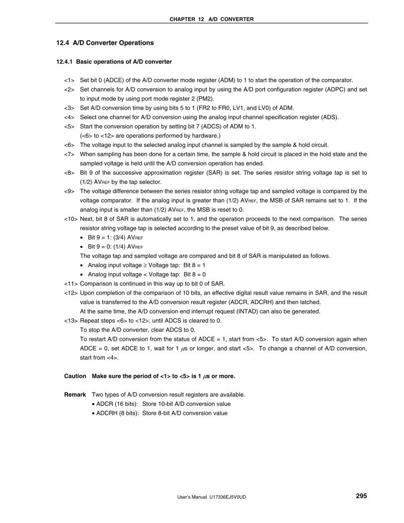
CHAPTER 12 A/D CONVERTER
User’s Manual U17336EJ5V0UD 295
12.4 A/D Converter Operations
12.4.1 Basic operations of A/D converter
<1> Set bit 0 (ADCE) of the A/D converter mode register (ADM) to 1 to start the operation of the comparator.
<2> Set channels for A/D conversion to analog input by using the A/D port configuration register (ADPC) and set
to input mode by using port mode register 2 (PM2).
<3> Set A/D conversion time by using bits 5 to 1 (FR2 to FR0, LV1, and LV0) of ADM.
<4> Select one channel for A/D conversion using the analog input channel specification register (ADS).
<5> Start the conversion operation by setting bit 7 (ADCS) of ADM to 1.
(<6> to <12> are operations performed by hardware.)
<6> The voltage input to the selected analog input channel is sampled by the sample & hold circuit.
<7> When sampling has been done for a certain time, the sample & hold circuit is placed in the hold state and the
sampled voltage is held until the A/D conversion operation has ended.
<8> Bit 9 of the successive approximation register (SAR) is set. The series resistor string voltage tap is set to
(1/2) AVREF by the tap selector.
<9> The voltage difference between the series resistor string voltage tap and sampled voltage is compared by the
voltage comparator. If the analog input is greater than (1/2) AVREF, the MSB of SAR remains set to 1. If the
analog input is smaller than (1/2) AVREF, the MSB is reset to 0.
<10> Next, bit 8 of SAR is automatically set to 1, and the operation proceeds to the next comparison. The series
resistor string voltage tap is selected according to the preset value of bit 9, as described below.
• Bit 9 = 1: (3/4) AVREF
• Bit 9 = 0: (1/4) AVREF
The voltage tap and sampled voltage are compared and bit 8 of SAR is manipulated as follows.
• Analog input voltage ≥ Voltage tap: Bit 8 = 1
• Analog input voltage < Voltage tap: Bit 8 = 0
<11> Comparison is continued in this way up to bit 0 of SAR.
<12> Upon completion of the comparison of 10 bits, an effective digital result value remains in SAR, and the result
value is transferred to the A/D conversion result register (ADCR, ADCRH) and then latched.
At the same time, the A/D conversion end interrupt request (INTAD) can also be generated.
<13> Repeat steps <6> to <12>, until ADCS is cleared to 0.
To stop the A/D converter, clear ADCS to 0.
To restart A/D conversion from the status of ADCE = 1, start from <5>. To start A/D conversion again when
ADCE = 0, set ADCE to 1, wait for 1 μs or longer, and start <5>. To change a channel of A/D conversion,
start from <4>.
Caution Make sure the period of <1> to <5> is 1 μs or more.
Remark Two types of A/D conversion result registers are available.
• ADCR (16 bits): Store 10-bit A/D conversion value
• ADCRH (8 bits): Store 8-bit A/D conversion value
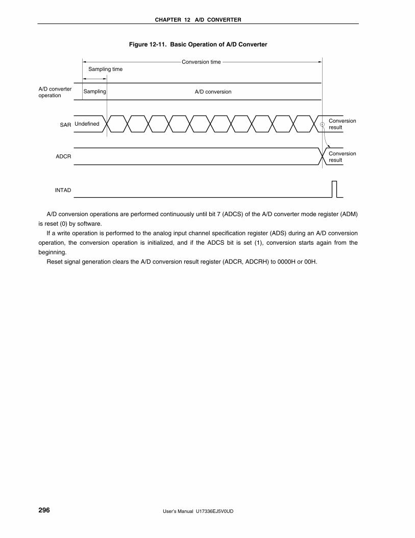
CHAPTER 12 A/D CONVERTER
User’s Manual U17336EJ5V0UD 296
Figure 12-11. Basic Operation of A/D Converter
Conversion time
Sampling time
Sampling A/D conversion
Undefined Conversion result
A/D converteroperation
SAR
ADCR
INTAD
Conversion result
A/D conversion operations are performed continuously until bit 7 (ADCS) of the A/D converter mode register (ADM)
is reset (0) by software.
If a write operation is performed to the analog input channel specification register (ADS) during an A/D conversion
operation, the conversion operation is initialized, and if the ADCS bit is set (1), conversion starts again from the
beginning.
Reset signal generation clears the A/D conversion result register (ADCR, ADCRH) to 0000H or 00H.

CHAPTER 12 A/D CONVERTER
User’s Manual U17336EJ5V0UD 297
12.4.2 Input voltage and conversion results
The relationship between the analog input voltage input to the analog input pins (ANI0 to ANI7Note) and the
theoretical A/D conversion result (stored in the 10-bit A/D conversion result register (ADCR)) is shown by the following
expression.
SAR = INT ( × 1024 + 0.5)
ADCR = SAR × 64
or
( − 0.5) × ≤ VAIN < ( + 0.5) ×
where, INT( ): Function which returns integer part of value in parentheses
VAIN: Analog input voltage
AVREF: AVREF pin voltage
ADCR: A/D conversion result register (ADCR) value
SAR: Successive approximation register
Note 38-pin products: ANI0 to ANI5
44-pin and 48-pin products: ANI0 to ANI7
Figure 12-12 shows the relationship between the analog input voltage and the A/D conversion result.
Figure 12-12. Relationship Between Analog Input Voltage and A/D Conversion Result
1023
1022
1021
3
2
1
0
FFC0H
FF80H
FF40H
00C0H
0080H
0040H
0000H
A/D conversion result
SAR ADCR
12048
11024
32048
21024
52048
Input voltage/AVREF
31024
20432048
10221024
20452048
10231024
20472048
1
VAIN
AVREF
AVREF
1024
AVREF
1024
ADCR
64
ADCR
64
<R>

CHAPTER 12 A/D CONVERTER
User’s Manual U17336EJ5V0UD 298
12.4.3 A/D converter operation mode
The operation mode of the A/D converter is the select mode. One channel of analog input is selected from ANI0 to
ANI7Note by the analog input channel specification register (ADS) and A/D conversion is executed.
Note 38-pin products: ANI0 to ANI5
44-pin and 48-pin products: ANI0 to ANI7
(1) A/D conversion operation
By setting bit 7 (ADCS) of the A/D converter mode register (ADM) to 1, the A/D conversion operation of the
voltage, which is applied to the analog input pin specified by the analog input channel specification register
(ADS), is started.
When A/D conversion has been completed, the result of the A/D conversion is stored in the A/D conversion result
register (ADCR), and an interrupt request signal (INTAD) is generated. When one A/D conversion has been
completed, the next A/D conversion operation is immediately started.
If ADS is rewritten during A/D conversion, the A/D conversion operation under execution is stopped and restarted
from the beginning.
If 0 is written to ADCS during A/D conversion, A/D conversion is immediately stopped. At this time, the
conversion result immediately before is retained.
Figure 12-13. A/D Conversion Operation
ANIn
Rewriting ADMADCS = 1 Rewriting ADS ADCS = 0
ANIn
ANIn ANIn ANIm
ANIn ANIm ANIm
StoppedConversion result immediately before is retained
A/D conversion
ADCR,ADCRH
INTAD
Conversion is stoppedConversion result immediately before is retained
Remarks 1. n = 0 to 5 (38-pin products), n = 0 to 7 (44-pin and 48-pin products)
2. m = 0 to 5 (38-pin products), m = 0 to 7 (44-pin and 48-pin products)
<R>
<R>

CHAPTER 12 A/D CONVERTER
User’s Manual U17336EJ5V0UD 299
The setting methods are described below.
<1> Set bit 0 (ADCE) of the A/D converter mode register (ADM) to 1.
<2> Set the channel to be used in the analog input mode by using bits 3 to 0 (ADPC3 to ADPC0) of the A/D
port configuration register (ADPC) and bits 7 to 0 (PM27 to PM20) of port mode register 2 (PM2).
<3> Select conversion time by using bits 5 to 1 (FR2 to FR0, LV1, and LV0) of ADM.
<4> Select a channel to be used by using bits 2 to 0 (ADS2 to ADS0) of the analog input channel
specification register (ADS).
<5> Set bit 7 (ADCS) of ADM to 1 to start A/D conversion.
<6> When one A/D conversion has been completed, an interrupt request signal (INTAD) is generated.
<7> Transfer the A/D conversion data to the A/D conversion result register (ADCR, ADCRH).
<Change the channel>
<8> Change the channel using bits 2 to 0 (ADS2 to ADS0) of ADS to start A/D conversion.
<9> When one A/D conversion has been completed, an interrupt request signal (INTAD) is generated.
<10> Transfer the A/D conversion data to the A/D conversion result register (ADCR, ADCRH).
<Complete A/D conversion>
<11> Clear ADCS to 0.
<12> Clear ADCE to 0.
Cautions 1. Make sure the period of <1> to <5> is 1 μs or more.
2. <1> may be done between <2> and <4>.
3. <1> can be omitted. However, ignore data of the first conversion after <5> in this case.
4. The period from <6> to <9> differs from the conversion time set using bits 5 to 1 (FR2 to
FR0, LV1, LV0) of ADM. The period from <8> to <9> is the conversion time set using FR2
to FR0, LV1, and LV0.
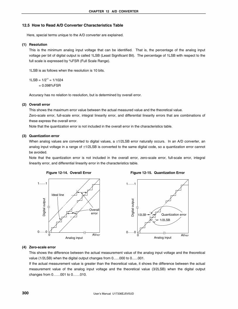
CHAPTER 12 A/D CONVERTER
User’s Manual U17336EJ5V0UD 300
12.5 How to Read A/D Converter Characteristics Table
Here, special terms unique to the A/D converter are explained.
(1) Resolution
This is the minimum analog input voltage that can be identified. That is, the percentage of the analog input
voltage per bit of digital output is called 1LSB (Least Significant Bit). The percentage of 1LSB with respect to the
full scale is expressed by %FSR (Full Scale Range).
1LSB is as follows when the resolution is 10 bits.
1LSB = 1/210 = 1/1024
= 0.098%FSR
Accuracy has no relation to resolution, but is determined by overall error.
(2) Overall error
This shows the maximum error value between the actual measured value and the theoretical value.
Zero-scale error, full-scale error, integral linearity error, and differential linearity errors that are combinations of
these express the overall error.
Note that the quantization error is not included in the overall error in the characteristics table.
(3) Quantization error
When analog values are converted to digital values, a ±1/2LSB error naturally occurs. In an A/D converter, an
analog input voltage in a range of ±1/2LSB is converted to the same digital code, so a quantization error cannot
be avoided.
Note that the quantization error is not included in the overall error, zero-scale error, full-scale error, integral
linearity error, and differential linearity error in the characteristics table.
Figure 12-14. Overall Error Figure 12-15. Quantization Error
Ideal line
0……0
1……1
Dig
ital o
utpu
t
Overallerror
Analog inputAVREF0
0……0
1……1
Dig
ital o
utpu
t
Quantization error1/2LSB
1/2LSB
Analog input0 AVREF
(4) Zero-scale error
This shows the difference between the actual measurement value of the analog input voltage and the theoretical
value (1/2LSB) when the digital output changes from 0......000 to 0......001.
If the actual measurement value is greater than the theoretical value, it shows the difference between the actual
measurement value of the analog input voltage and the theoretical value (3/2LSB) when the digital output
changes from 0……001 to 0……010.
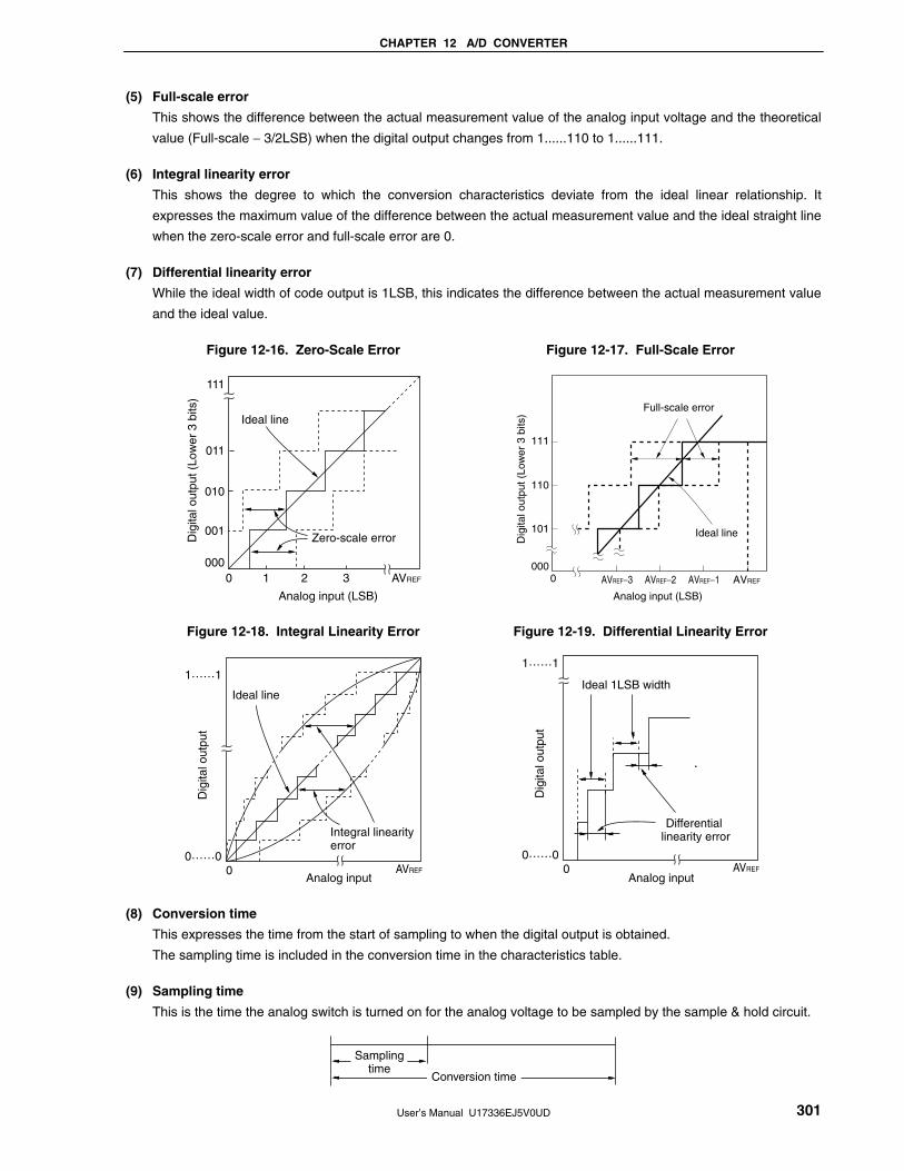
CHAPTER 12 A/D CONVERTER
User’s Manual U17336EJ5V0UD 301
(5) Full-scale error
This shows the difference between the actual measurement value of the analog input voltage and the theoretical
value (Full-scale − 3/2LSB) when the digital output changes from 1......110 to 1......111.
(6) Integral linearity error
This shows the degree to which the conversion characteristics deviate from the ideal linear relationship. It
expresses the maximum value of the difference between the actual measurement value and the ideal straight line
when the zero-scale error and full-scale error are 0.
(7) Differential linearity error
While the ideal width of code output is 1LSB, this indicates the difference between the actual measurement value
and the ideal value.
Figure 12-16. Zero-Scale Error Figure 12-17. Full-Scale Error
111
011
010
001Zero-scale error
Ideal line
0000 1 2 3 AVREF
Dig
ital o
utpu
t (Lo
wer
3 b
its)
Analog input (LSB)
111
110
101
0000 AVREF−3
Full-scale error
Ideal line
Analog input (LSB)
Dig
ital o
utpu
t (Lo
wer
3 b
its)
AVREF−2 AVREF−1 AVREF
Figure 12-18. Integral Linearity Error Figure 12-19. Differential Linearity Error
0 AVREF
Dig
ital o
utpu
t
Analog input
Integral linearityerror
Ideal line
1……1
0……0
0 AVREF
Dig
ital o
utpu
t
Analog input
Differential linearity error
1……1
0……0
Ideal 1LSB width
(8) Conversion time
This expresses the time from the start of sampling to when the digital output is obtained.
The sampling time is included in the conversion time in the characteristics table.
(9) Sampling time
This is the time the analog switch is turned on for the analog voltage to be sampled by the sample & hold circuit.
Samplingtime
Conversion time

CHAPTER 12 A/D CONVERTER
User’s Manual U17336EJ5V0UD 302
12.6 Cautions for A/D Converter
(1) Operating current in STOP mode
The A/D converter stops operating in the STOP mode. At this time, the operating current can be reduced by
clearing bit 7 (ADCS) and bit 0 (ADCE) of the A/D converter mode register (ADM) to 0.
To restart from the standby status, clear bit 0 (ADIF) of interrupt request flag register 1L (IF1L) to 0 and start
operation.
(2) Input range of ANI0 to ANI7Note
Observe the rated range of the ANI0 to ANI7Note input voltage. If a voltage of AVREF or higher and AVSS or lower
(even in the range of absolute maximum ratings) is input to an analog input channel, the converted value of that
channel becomes undefined. In addition, the converted values of the other channels may also be affected.
(3) Conflicting operations
<1> Conflict between A/D conversion result register (ADCR, ADCRH) write and ADCR or ADCRH read by
instruction upon the end of conversion
ADCR or ADCRH read has priority. After the read operation, the new conversion result is written to ADCR
or ADCRH.
<2> Conflict between ADCR or ADCRH write and A/D converter mode register (ADM) write, analog input
channel specification register (ADS), or A/D port configuration register (ADPC) write upon the end of
conversion
ADM, ADS, or ADPC write has priority. ADCR or ADCRH write is not performed, nor is the conversion end
interrupt signal (INTAD) generated.
(4) Noise countermeasures
To maintain the 10-bit resolution, attention must be paid to noise input to the AVREF pin and ANI0 to ANI7 pinsNote.
<1> Connect a capacitor with a low equivalent resistance and a good frequency response to the power supply.
<2> The higher the output impedance of the analog input source, the greater the influence. To reduce the
noise, connecting external C as shown in Figure 12-20 is recommended.
<3> Do not switch these pins with other pins during conversion.
<4> The accuracy is improved if the HALT mode is set immediately after the start of conversion.
Note 38-pin products: ANI0 to ANI5 pins
44-pin and 48-pin products: ANI0 to ANI7 pins
<R>

CHAPTER 12 A/D CONVERTER
User’s Manual U17336EJ5V0UD 303
Figure 12-20. Analog Input Pin Connection
Referencevoltage
input
C = 100 to 1,000 pF
If there is a possibility that noise equal to or higher than AVREF or equal to or lower than AVSS may enter, clamp with a diode with a small VF value (0.3 V or lower).
AVREF
AVSS
VSS
ANI0 to ANI7Note
(5) ANI0/P20 to ANI7/P27Note
<1> The analog input pins (ANI0 to ANI7Note) are also used as input port pins (P20 to P27Note).
When A/D conversion is performed with any of ANI0 to ANI7Note selected, do not access P20 to P27Note while
conversion is in progress; otherwise the conversion resolution may be degraded. It is recommended to
select pins used as P20 to P27Note starting with the ANI0/P20 that is the furthest from AVREF.
<2> If a digital pulse is applied to the pins adjacent to the pins currently used for A/D conversion, the expected
value of the A/D conversion may not be obtained due to coupling noise. Therefore, do not apply a pulse to
the pins adjacent to the pin undergoing A/D conversion.
(6) Input impedance of ANI0 to ANI7 pinsNote
This A/D converter charges a sampling capacitor for sampling during sampling time.
Therefore, only a leakage current flows when sampling is not in progress, and a current that charges the
capacitor flows during sampling. Consequently, the input impedance fluctuates depending on whether sampling
is in progress, and on the other states.
To make sure that sampling is effective, however, it is recommended to keep the output impedance of the analog
input source to within 10 kΩ, and to connect a capacitor of about 100 pF to the ANI0 to ANI7 pinsNote (see Figure
12-20).
(7) AVREF pin input impedance
A series resistor string of several tens of kΩ is connected between the AVREF and AVSS pins.
Therefore, if the output impedance of the reference voltage source is high, this will result in a series connection to
the series resistor string between the AVREF and AVSS pins, resulting in a large reference voltage error.
Note 38-pin products: ANI0/P20 to ANI5/P25 pins
44-pin and 48-pin products: ANI0/P20 to ANI7/P27 pins
<R>

CHAPTER 12 A/D CONVERTER
User’s Manual U17336EJ5V0UD 304
(8) Interrupt request flag (ADIF)
The interrupt request flag (ADIF) is not cleared even if the analog input channel specification register (ADS) is
changed.
Therefore, if an analog input pin is changed during A/D conversion, the A/D conversion result and ADIF for the
pre-change analog input may be set just before the ADS rewrite. Caution is therefore required since, at this time,
when ADIF is read immediately after the ADS rewrite, ADIF is set despite the fact A/D conversion for the post-
change analog input has not ended.
When A/D conversion is stopped and then resumed, clear ADIF before the A/D conversion operation is resumed.
Figure 12-21. Timing of A/D Conversion End Interrupt Request Generation
ADS rewrite (start of ANIn conversion)
A/D conversion
ADCR
ADIF
ANIn ANIn ANIm ANIm
ANIn ANIn ANIm ANIm
ADS rewrite (start of ANIm conversion)
ADIF is set but ANIm conversion has not ended.
Remarks 1. n = 0 to 5 (38-pin products), n = 0 to 7 (44-pin and 48-pin products)
2. m = 0 to 5 (38-pin products), m = 0 to 7 (44-pin and 48-pin products)
(9) Conversion results just after A/D conversion start
The first A/D conversion value immediately after A/D conversion starts may not fall within the rating range if the
ADCS bit is set to 1 within 1 μs after the ADCE bit was set to 1, or if the ADCS bit is set to 1 with the ADCE bit =
0. Take measures such as polling the A/D conversion end interrupt request (INTAD) and removing the first
conversion result.
(10) A/D conversion result register (ADCR, ADCRH) read operation
When a write operation is performed to the A/D converter mode register (ADM), analog input channel
specification register (ADS), and A/D port configuration register (ADPC), the contents of ADCR and ADCRH may
become undefined. Read the conversion result following conversion completion before writing to ADM, ADS, and
ADPC. Using a timing other than the above may cause an incorrect conversion result to be read.
<R>
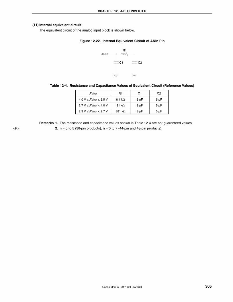
CHAPTER 12 A/D CONVERTER
User’s Manual U17336EJ5V0UD 305
(11) Internal equivalent circuit
The equivalent circuit of the analog input block is shown below.
Figure 12-22. Internal Equivalent Circuit of ANIn Pin
ANIn
C1 C2
R1
Table 12-4. Resistance and Capacitance Values of Equivalent Circuit (Reference Values)
AVREF R1 C1 C2
4.0 V ≤ AVREF ≤ 5.5 V 8.1 kΩ 8 pF 5 pF
2.7 V ≤ AVREF < 4.0 V 31 kΩ 8 pF 5 pF
2.3 V ≤ AVREF < 2.7 V 381 kΩ 8 pF 5 pF
Remarks 1. The resistance and capacitance values shown in Table 12-4 are not guaranteed values.
2. n = 0 to 5 (38-pin products), n = 0 to 7 (44-pin and 48-pin products)
<R>

User’s Manual U17336EJ5V0UD 306
CHAPTER 13 SERIAL INTERFACE UART0
13.1 Functions of Serial Interface UART0
Serial interface UART0 has the following two modes.
(1) Operation stop mode
This mode is used when serial communication is not executed and can enable a reduction in the power
consumption.
For details, see 13.4.1 Operation stop mode.
(2) Asynchronous serial interface (UART) mode
The functions of this mode are outlined below.
For details, see 13.4.2 Asynchronous serial interface (UART) mode and 13.4.3 Dedicated baud rate
generator.
• Maximum transfer rate: 625 kbps
• Two-pin configuration TXD0: Transmit data output pin
RXD0: Receive data input pin
• Length of communication data can be selected from 7 or 8 bits.
• Dedicated on-chip 5-bit baud rate generator allowing any baud rate to be set
• Transmission and reception can be performed independently (full-duplex operation).
• Fixed to LSB-first communication
Cautions 1. If clock supply to serial interface UART0 is not stopped (e.g., in the HALT mode), normal
operation continues. If clock supply to serial interface UART0 is stopped (e.g., in the STOP
mode), each register stops operating, and holds the value immediately before clock supply
was stopped. The TXD0 pin also holds the value immediately before clock supply was
stopped and outputs it. However, the operation is not guaranteed after clock supply is
resumed. Therefore, reset the circuit so that POWER0 = 0, RXE0 = 0, and TXE0 = 0.
2. Set POWER0 = 1 and then set TXE0 = 1 (transmission) or RXE0 = 1 (reception) to start
communication.
3. TXE0 and RXE0 are synchronized by the base clock (fXCLK0) set by BRGC0. To enable
transmission or reception again, set TXE0 or RXE0 to 1 at least two clocks of base clock
after TXE0 or RXE0 has been cleared to 0. If TXE0 or RXE0 is set within two clocks of base
clock, the transmission circuit or reception circuit may not be initialized.
4. Set transmit data to TXS0 at least one base clock (fXCLK0) after setting TXE0 = 1.

CHAPTER 13 SERIAL INTERFACE UART0
User’s Manual U17336EJ5V0UD 307
13.2 Configuration of Serial Interface UART0
Serial interface UART0 includes the following hardware.
Table 13-1. Configuration of Serial Interface UART0
Item Configuration
Registers Receive buffer register 0 (RXB0)
Receive shift register 0 (RXS0)
Transmit shift register 0 (TXS0)
Control registers Asynchronous serial interface operation mode register 0 (ASIM0)
Asynchronous serial interface reception error status register 0 (ASIS0)
Baud rate generator control register 0 (BRGC0)
Port mode register 1 (PM1)
Port register 1 (P1)

CH
AP
TE
R 13 S
ER
IAL
INT
ER
FA
CE
UA
RT
0
User’s M
anual U17336E
J5V0U
D
308 <R> Figure 13-1. Block Diagram of Serial Interface UART0
TXD0/SCK10/P10
INTST0
fXCLK0
RXD0/SI10/P11
INTSR0
fPRS/25
fPRS/23
fPRS/2
Transmit shift register 0 (TXS0)
Receive shift register 0 (RXS0)
Receive buffer register 0(RXB0)
Asynchronous serial interface reception error status register 0 (ASIS0)
Asynchronous serial interface operation mode
register 0 (ASIM0)
Baud rate generator control register 0
(BRGC0)
8-bit timer/event counter50 output
Registers
Sel
ecto
r
Baud rate generator
Baud rate generator
Reception unit
Reception control
Filter
Internal bus
Transmission control
Transmission unit
Output latch(P10)
PM10
7 7

CHAPTER 13 SERIAL INTERFACE UART0
User’s Manual U17336EJ5V0UD 309
(1) Receive buffer register 0 (RXB0)
This 8-bit register stores parallel data converted by receive shift register 0 (RXS0).
Each time 1 byte of data has been received, new receive data is transferred to this register from receive shift
register 0 (RXS0).
If the data length is set to 7 bits the receive data is transferred to bits 0 to 6 of RXB0 and the MSB of RXB0 is
always 0.
If an overrun error (OVE0) occurs, the receive data is not transferred to RXB0.
RXB0 can be read by an 8-bit memory manipulation instruction. No data can be written to this register.
Reset signal generation and POWER0 = 0 set this register to FFH.
(2) Receive shift register 0 (RXS0)
This register converts the serial data input to the RXD0 pin into parallel data.
RXS0 cannot be directly manipulated by a program.
(3) Transmit shift register 0 (TXS0)
This register is used to set transmit data. Transmission is started when data is written to TXS0, and serial data is
transmitted from the TXD0 pins.
TXS0 can be written by an 8-bit memory manipulation instruction. This register cannot be read.
Reset signal generation, POWER0 = 0, and TXE0 = 0 set this register to FFH.
Cautions 1. Set transmit data to TXS0 at least one base clock (fXCLK0) after setting TXE0 = 1.
2. Do not write the next transmit data to TXS0 before the transmission completion interrupt
signal (INTST0) is generated.
CHAPTER 13 SERIAL INTERFACE UART0
User’s Manual U17336EJ5V0UD 310
13.3 Registers Controlling Serial Interface UART0
Serial interface UART0 is controlled by the following five registers.
• Asynchronous serial interface operation mode register 0 (ASIM0)
• Asynchronous serial interface reception error status register 0 (ASIS0)
• Baud rate generator control register 0 (BRGC0)
• Port mode register 1 (PM1)
• Port register 1 (P1)
(1) Asynchronous serial interface operation mode register 0 (ASIM0)
This 8-bit register controls the serial communication operations of serial interface UART0.
This register can be set by a 1-bit or 8-bit memory manipulation instruction.
Reset signal generation sets this register to 01H.
Figure 13-2. Format of Asynchronous Serial Interface Operation Mode Register 0 (ASIM0) (1/2)
Address: FF70H After reset: 01H R/W
Symbol <7> <6> <5> 4 3 2 1 0
ASIM0 POWER0 TXE0 RXE0 PS01 PS00 CL0 SL0 1
POWER0 Enables/disables operation of internal operation clock
0Note 1 Disables operation of the internal operation clock (fixes the clock to low level) and asynchronously
resets the internal circuitNote 2.
1 Enables operation of the internal operation clock.
TXE0 Enables/disables transmission
0 Disables transmission (synchronously resets the transmission circuit).
1 Enables transmission.
RXE0 Enables/disables reception
0 Disables reception (synchronously resets the reception circuit).
1 Enables reception.
Notes 1. The input from the RXD0 pin is fixed to high level when POWER0 = 0.
2. Asynchronous serial interface reception error status register 0 (ASIS0), transmit shift register 0 (TXS0),
and receive buffer register 0 (RXB0) are reset.

CHAPTER 13 SERIAL INTERFACE UART0
User’s Manual U17336EJ5V0UD 311
Figure 13-2. Format of Asynchronous Serial Interface Operation Mode Register 0 (ASIM0) (2/2)
PS01 PS00 Transmission operation Reception operation
0 0 Does not output parity bit. Reception without parity
0 1 Outputs 0 parity. Reception as 0 parityNote
1 0 Outputs odd parity. Judges as odd parity.
1 1 Outputs even parity. Judges as even parity.
CL0 Specifies character length of transmit/receive data
0 Character length of data = 7 bits
1 Character length of data = 8 bits
SL0 Specifies number of stop bits of transmit data
0 Number of stop bits = 1
1 Number of stop bits = 2
Note If “reception as 0 parity” is selected, the parity is not judged. Therefore, bit 2 (PE0) of asynchronous serial
interface reception error status register 0 (ASIS0) is not set and the error interrupt does not occur.
Cautions 1. To start the transmission, set POWER0 to 1 and then set TXE0 to 1. To stop the transmission,
clear TXE0 to 0, and then clear POWER0 to 0.
2. To start the reception, set POWER0 to 1 and then set RXE0 to 1. To stop the reception, clear
RXE0 to 0, and then clear POWER0 to 0.
3. Set POWER0 to 1 and then set RXE0 to 1 while a high level is input to the RxD0 pin. If
POWER0 is set to 1 and RXE0 is set to 1 while a low level is input, reception is started.
4. TXE0 and RXE0 are synchronized by the base clock (fXCLK0) set by BRGC0. To enable
transmission or reception again, set TXE0 or RXE0 to 1 at least two clocks of base clock after
TXE0 or RXE0 has been cleared to 0. If TXE0 or RXE0 is set within two clocks of base clock,
the transmission circuit or reception circuit may not be initialized.
5. Set transmit data to TXS0 at least one base clock (fXCLK0) after setting TXE0 = 1.
6. Clear the TXE0 and RXE0 bits to 0 before rewriting the PS01, PS00, and CL0 bits.
7. Make sure that TXE0 = 0 when rewriting the SL0 bit. Reception is always performed with
“number of stop bits = 1”, and therefore, is not affected by the set value of the SL0 bit.
8. Be sure to set bit 0 to 1.

CHAPTER 13 SERIAL INTERFACE UART0
User’s Manual U17336EJ5V0UD 312
(2) Asynchronous serial interface reception error status register 0 (ASIS0)
This register indicates an error status on completion of reception by serial interface UART0. It includes three
error flag bits (PE0, FE0, OVE0).
This register is read-only by an 8-bit memory manipulation instruction.
Reset signal generation, or clearing bit 7 (POWER0) or bit 5 (RXE0) of ASIM0 to 0 clears this register to 00H.
00H is read when this register is read. If a reception error occurs, read ASIS0 and then read receive buffer
register 0 (RXB0) to clear the error flag.
Figure 13-3. Format of Asynchronous Serial Interface Reception Error Status Register 0 (ASIS0)
Address: FF73H After reset: 00H R
Symbol 7 6 5 4 3 2 1 0
ASIS0 0 0 0 0 0 PE0 FE0 OVE0
PE0 Status flag indicating parity error
0 If POWER0 = 0 or RXE0 = 0, or if ASIS0 register is read.
1 If the parity of transmit data does not match the parity bit on completion of reception.
FE0 Status flag indicating framing error
0 If POWER0 = 0 or RXE0 = 0, or if ASIS0 register is read.
1 If the stop bit is not detected on completion of reception.
OVE0 Status flag indicating overrun error
0 If POWER0 = 0 or RXE0 = 0, or if ASIS0 register is read.
1 If receive data is set to the RXB0 register and the next reception operation is completed before the
data is read.
Cautions 1. The operation of the PE0 bit differs depending on the set values of the PS01 and PS00 bits of
asynchronous serial interface operation mode register 0 (ASIM0).
2. For the stop bit of the receive data, only the first stop bit is checked regardless of the number
of stop bits.
3. If an overrun error occurs, the next receive data is not written to receive buffer register 0
(RXB0) but discarded.
4. If data is read from ASIS0, a wait cycle is generated. Do not read data from ASIS0 when the
CPU is operating on the subsystem clock and the peripheral hardware clock is stopped. For
details, see CHAPTER 34 CAUTIONS FOR WAIT.
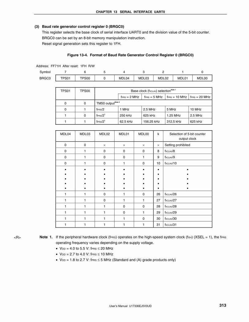
CHAPTER 13 SERIAL INTERFACE UART0
User’s Manual U17336EJ5V0UD 313
(3) Baud rate generator control register 0 (BRGC0)
This register selects the base clock of serial interface UART0 and the division value of the 5-bit counter.
BRGC0 can be set by an 8-bit memory manipulation instruction.
Reset signal generation sets this register to 1FH.
Figure 13-4. Format of Baud Rate Generator Control Register 0 (BRGC0)
Address: FF71H After reset: 1FH R/W
Symbol 7 6 5 4 3 2 1 0
BRGC0 TPS01 TPS00 0 MDL04 MDL03 MDL02 MDL01 MDL00
Base clock (fXCLK0) selectionNote 1 TPS01 TPS00
fPRS = 2 MHz fPRS = 5 MHz fPRS = 10 MHz fPRS = 20 MHz
0 0 TM50 outputNote 2
0 1 fPRS/2 1 MHz 2.5 MHz 5 MHz 10 MHz
1 0 fPRS/23 250 kHz 625 kHz 1.25 MHz 2.5 MHz
1 1 fPRS/25 62.5 kHz 156.25 kHz 312.5 kHz 625 kHz
MDL04 MDL03 MDL02 MDL01 MDL00 k Selection of 5-bit counter output clock
0 0 × × × × Setting prohibited
0 1 0 0 0 8 fXCLK0/8
0 1 0 0 1 9 fXCLK0/9
0 1 0 1 0 10 fXCLK0/10
• • • •
•
• • • •
•
• • • •
•
• • • •
•
• • • •
•
• • • •
•
• • • •
•
1 1 0 1 0 26 fXCLK0/26
1 1 0 1 1 27 fXCLK0/27
1 1 1 0 0 28 fXCLK0/28
1 1 1 0 1 29 fXCLK0/29
1 1 1 1 0 30 fXCLK0/30
1 1 1 1 1 31 fXCLK0/31
Note 1. If the peripheral hardware clock (fPRS) operates on the high-speed system clock (fXH) (XSEL = 1), the fPRS
operating frequency varies depending on the supply voltage.
• VDD = 4.0 to 5.5 V: fPRS ≤ 20 MHz
• VDD = 2.7 to 4.0 V: fPRS ≤ 10 MHz
• VDD = 1.8 to 2.7 V: fPRS ≤ 5 MHz (Standard and (A) grade products only)
<R>
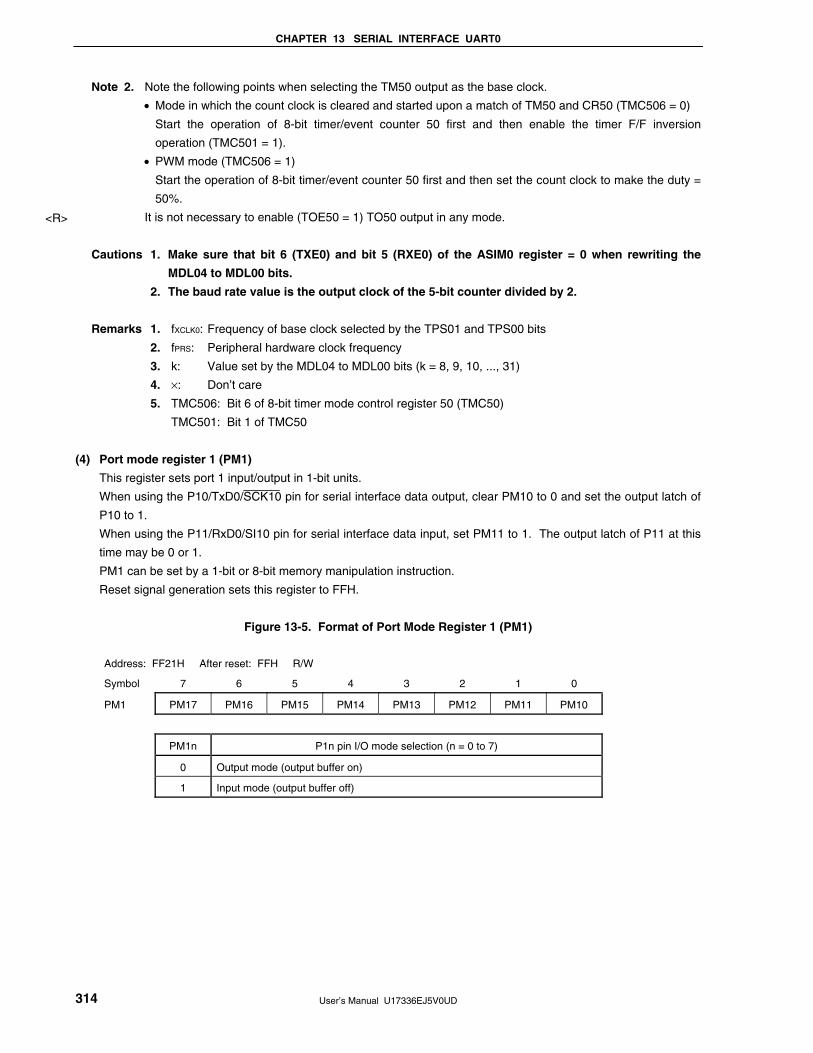
CHAPTER 13 SERIAL INTERFACE UART0
User’s Manual U17336EJ5V0UD 314
Note 2. Note the following points when selecting the TM50 output as the base clock.
• Mode in which the count clock is cleared and started upon a match of TM50 and CR50 (TMC506 = 0)
Start the operation of 8-bit timer/event counter 50 first and then enable the timer F/F inversion
operation (TMC501 = 1).
• PWM mode (TMC506 = 1)
Start the operation of 8-bit timer/event counter 50 first and then set the count clock to make the duty =
50%.
It is not necessary to enable (TOE50 = 1) TO50 output in any mode.
Cautions 1. Make sure that bit 6 (TXE0) and bit 5 (RXE0) of the ASIM0 register = 0 when rewriting the
MDL04 to MDL00 bits.
2. The baud rate value is the output clock of the 5-bit counter divided by 2.
Remarks 1. fXCLK0: Frequency of base clock selected by the TPS01 and TPS00 bits
2. fPRS: Peripheral hardware clock frequency
3. k: Value set by the MDL04 to MDL00 bits (k = 8, 9, 10, ..., 31)
4. ×: Don’t care
5. TMC506: Bit 6 of 8-bit timer mode control register 50 (TMC50)
TMC501: Bit 1 of TMC50
(4) Port mode register 1 (PM1)
This register sets port 1 input/output in 1-bit units.
When using the P10/TxD0/SCK10 pin for serial interface data output, clear PM10 to 0 and set the output latch of
P10 to 1.
When using the P11/RxD0/SI10 pin for serial interface data input, set PM11 to 1. The output latch of P11 at this
time may be 0 or 1.
PM1 can be set by a 1-bit or 8-bit memory manipulation instruction.
Reset signal generation sets this register to FFH.
Figure 13-5. Format of Port Mode Register 1 (PM1)
Address: FF21H After reset: FFH R/W
Symbol 7 6 5 4 3 2 1 0
PM1 PM17 PM16 PM15 PM14 PM13 PM12 PM11 PM10
PM1n P1n pin I/O mode selection (n = 0 to 7)
0 Output mode (output buffer on)
1 Input mode (output buffer off)
<R>

CHAPTER 13 SERIAL INTERFACE UART0
User’s Manual U17336EJ5V0UD 315
13.4 Operation of Serial Interface UART0
Serial interface UART0 has the following two modes.
• Operation stop mode
• Asynchronous serial interface (UART) mode
13.4.1 Operation stop mode
In this mode, serial communication cannot be executed, thus reducing the power consumption. In addition, the
pins can be used as ordinary port pins in this mode. To set the operation stop mode, clear bits 7, 6, and 5 (POWER0,
TXE0, and RXE0) of ASIM0 to 0.
(1) Register used
The operation stop mode is set by asynchronous serial interface operation mode register 0 (ASIM0).
ASIM0 can be set by a 1-bit or 8-bit memory manipulation instruction.
Reset signal generation sets this register to 01H.
Address: FF70H After reset: 01H R/W
Symbol <7> <6> <5> 4 3 2 1 0
ASIM0 POWER0 TXE0 RXE0 PS01 PS00 CL0 SL0 1
POWER0 Enables/disables operation of internal operation clock
0Note 1 Disables operation of the internal operation clock (fixes the clock to low level) and asynchronously
resets the internal circuitNote 2.
TXE0 Enables/disables transmission
0 Disables transmission (synchronously resets the transmission circuit).
RXE0 Enables/disables reception
0 Disables reception (synchronously resets the reception circuit).
Notes 1. The input from the RXD0 pin is fixed to high level when POWER0 = 0.
2. Asynchronous serial interface reception error status register 0 (ASIS0), transmit shift register 0 (TXS0),
and receive buffer register 0 (RXB0) are reset.
Caution Clear POWER0 to 0 after clearing TXE0 and RXE0 to 0 to set the operation stop mode.
To start the communication, set POWER0 to 1, and then set TXE0 or RXE0 to 1.
Remark To use the RxD0/SI10/P11 and TxD0/SCK10/P10 pins as general-purpose port pins, see CHAPTER 4
PORT FUNCTIONS.
CHAPTER 13 SERIAL INTERFACE UART0
User’s Manual U17336EJ5V0UD 316
13.4.2 Asynchronous serial interface (UART) mode
In this mode, 1-byte data is transmitted/received following a start bit, and a full-duplex operation can be performed.
A dedicated UART baud rate generator is incorporated, so that communication can be executed at a wide range of
baud rates.
(1) Registers used
• Asynchronous serial interface operation mode register 0 (ASIM0)
• Asynchronous serial interface reception error status register 0 (ASIS0)
• Baud rate generator control register 0 (BRGC0)
• Port mode register 1 (PM1)
• Port register 1 (P1)
The basic procedure of setting an operation in the UART mode is as follows.
<1> Set the BRGC0 register (see Figure 13-4).
<2> Set bits 1 to 4 (SL0, CL0, PS00, and PS01) of the ASIM0 register (see Figure 13-2).
<3> Set bit 7 (POWER0) of the ASIM0 register to 1.
<4> Set bit 6 (TXE0) of the ASIM0 register to 1. → Transmission is enabled.
Set bit 5 (RXE0) of the ASIM0 register to 1. → Reception is enabled.
<5> Write data to the TXS0 register. → Data transmission is started.
Caution Take relationship with the other party of communication when setting the port mode register
and port register.
The relationship between the register settings and pins is shown below.
Table 13-2. Relationship Between Register Settings and Pins
Pin Function POWER0 TXE0 RXE0 PM10 P10 PM11 P11 UART0
Operation TxD0/SCK10/P10 RxD0/SI10/P11
0 0 0 ×Note ×Note ×Note ×Note Stop SCK10/P10 SI10/P11
0 1 ×Note ×Note 1 × Reception SCK10/P10 RxD0
1 0 0 1 ×Note ×Note Transmission TxD0 SI10/P11
1
1 1 0 1 1 × Transmission/
reception
TxD0 RxD0
Note Can be set as port function or serial interface CSI10.
Remark ×: don’t care
POWER0: Bit 7 of asynchronous serial interface operation mode register 0 (ASIM0)
TXE0: Bit 6 of ASIM0
RXE0: Bit 5 of ASIM0
PM1×: Port mode register
P1×: Port output latch

CHAPTER 13 SERIAL INTERFACE UART0
User’s Manual U17336EJ5V0UD 317
(2) Communication operation
(a) Format and waveform example of normal transmit/receive data
Figures 13-6 and 13-7 show the format and waveform example of the normal transmit/receive data.
Figure 13-6. Format of Normal UART Transmit/Receive Data
Start bit
Parity bit
D0 D1 D2 D3 D4
1 data frame
Character bits
D5 D6 D7 Stop bit
One data frame consists of the following bits.
• Start bit ... 1 bit
• Character bits ... 7 or 8 bits (LSB first)
• Parity bit ... Even parity, odd parity, 0 parity, or no parity
• Stop bit ... 1 or 2 bits
The character bit length, parity, and stop bit length in one data frame are specified by asynchronous serial
interface operation mode register 0 (ASIM0).
Figure 13-7. Example of Normal UART Transmit/Receive Data Waveform
1. Data length: 8 bits, Parity: Even parity, Stop bit: 1 bit, Communication data: 55H
1 data frame
Start D0 D1 D2 D3 D4 D5 D6 D7 Parity Stop
2. Data length: 7 bits, Parity: Odd parity, Stop bit: 2 bits, Communication data: 36H
1 data frame
Start D0 D1 D2 D3 D4 D5 D6 Parity StopStop
3. Data length: 8 bits, Parity: None, Stop bit: 1 bit, Communication data: 87H
1 data frame
Start D0 D1 D2 D3 D4 D5 D6 D7 Stop

CHAPTER 13 SERIAL INTERFACE UART0
User’s Manual U17336EJ5V0UD 318
(b) Parity types and operation
The parity bit is used to detect a bit error in communication data. Usually, the same type of parity bit is used
on both the transmission and reception sides. With even parity and odd parity, a 1-bit (odd number) error
can be detected. With zero parity and no parity, an error cannot be detected.
(i) Even parity
• Transmission
Transmit data, including the parity bit, is controlled so that the number of bits that are “1” is even.
The value of the parity bit is as follows.
If transmit data has an odd number of bits that are “1”: 1
If transmit data has an even number of bits that are “1”: 0
• Reception
The number of bits that are “1” in the receive data, including the parity bit, is counted. If it is odd, a
parity error occurs.
(ii) Odd parity
• Transmission
Unlike even parity, transmit data, including the parity bit, is controlled so that the number of bits that
are “1” is odd.
If transmit data has an odd number of bits that are “1”: 0
If transmit data has an even number of bits that are “1”: 1
• Reception
The number of bits that are “1” in the receive data, including the parity bit, is counted. If it is even, a
parity error occurs.
(iii) 0 parity
The parity bit is cleared to 0 when data is transmitted, regardless of the transmit data.
The parity bit is not detected when the data is received. Therefore, a parity error does not occur
regardless of whether the parity bit is “0” or “1”.
(iv) No parity
No parity bit is appended to the transmit data.
Reception is performed assuming that there is no parity bit when data is received. Because there is no
parity bit, a parity error does not occur.

CHAPTER 13 SERIAL INTERFACE UART0
User’s Manual U17336EJ5V0UD 319
(c) Transmission
If bit 7 (POWER0) of asynchronous serial interface operation mode register 0 (ASIM0) is set to 1 and bit 6
(TXE0) of ASIM0 is then set to 1, transmission is enabled. Transmission can be started by writing transmit
data to transmit shift register 0 (TXS0). The start bit, parity bit, and stop bit are automatically appended to
the data.
When transmission is started, the start bit is output from the TXD0 pin, and the transmit data is output
followed by the rest of the data in order starting from the LSB. When transmission is completed, the parity
and stop bits set by ASIM0 are appended and a transmission completion interrupt request (INTST0) is
generated.
Transmission is stopped until the data to be transmitted next is written to TXS0.
Figure 13-8 shows the timing of the transmission completion interrupt request (INTST0). This interrupt
occurs as soon as the last stop bit has been output.
Caution After transmit data is written to TXS0, do not write the next transmit data before the
transmission completion interrupt signal (INTST0) is generated.
Figure 13-8. Transmission Completion Interrupt Request Timing
1. Stop bit length: 1
INTST0
D0Start D1 D2 D6 D7 StopTXD0 (output) Parity
2. Stop bit length: 2
TXD0 (output)
INTST0
D0Start D1 D2 D6 D7 Parity Stop

CHAPTER 13 SERIAL INTERFACE UART0
User’s Manual U17336EJ5V0UD 320
(d) Reception
Reception is enabled and the RXD0 pin input is sampled when bit 7 (POWER0) of asynchronous serial
interface operation mode register 0 (ASIM0) is set to 1 and then bit 5 (RXE0) of ASIM0 is set to 1.
The 5-bit counter of the baud rate generator starts counting when the falling edge of the RXD0 pin input is
detected. When the set value of baud rate generator control register 0 (BRGC0) has been counted, the
RXD0 pin input is sampled again ( in Figure 13-9). If the RXD0 pin is low level at this time, it is recognized
as a start bit.
When the start bit is detected, reception is started, and serial data is sequentially stored in receive shift
register 0 (RXS0) at the set baud rate. When the stop bit has been received, the reception completion
interrupt (INTSR0) is generated and the data of RXS0 is written to receive buffer register 0 (RXB0). If an
overrun error (OVE0) occurs, however, the receive data is not written to RXB0.
Even if a parity error (PE0) occurs while reception is in progress, reception continues to the reception
position of the stop bit, and an reception error interrupt (INTSR0) is generated after completion of reception.
INTSR0 occurs upon completion of reception and in case of a reception error.
Figure 13-9. Reception Completion Interrupt Request Timing
RXD0 (input)
INTSR0
Start D0 D1 D2 D3 D4 D5 D6 D7 Parity Stop
RXB0
Cautions 1. If a reception error occurs, read asynchronous serial interface reception error status
register 0 (ASIS0) and then read receive buffer register 0 (RXB0) to clear the error flag.
Otherwise, an overrun error will occur when the next data is received, and the reception
error status will persist.
2. Reception is always performed with the “number of stop bits = 1”. The second stop bit
is ignored.

CHAPTER 13 SERIAL INTERFACE UART0
User’s Manual U17336EJ5V0UD 321
(e) Reception error
Three types of errors may occur during reception: a parity error, framing error, or overrun error. If the error
flag of asynchronous serial interface reception error status register 0 (ASIS0) is set as a result of data
reception, a reception error interrupt (INTSR0) is generated.
Which error has occurred during reception can be identified by reading the contents of ASIS0 in the reception
error interrupt (INTSR0) servicing (see Figure 13-3).
The contents of ASIS0 are cleared to 0 when ASIS0 is read.
Table 13-3. Cause of Reception Error
Reception Error Cause
Parity error The parity specified for transmission does not match the parity of the receive data.
Framing error Stop bit is not detected.
Overrun error Reception of the next data is completed before data is read from receive buffer
register 0 (RXB0).
(f) Noise filter of receive data
The RXD0 signal is sampled using the base clock output by the prescaler block.
If two sampled values are the same, the output of the match detector changes, and the data is sampled as
input data.
Because the circuit is configured as shown in Figure 13-10, the internal processing of the reception operation
is delayed by two clocks from the external signal status.
Figure 13-10. Noise Filter Circuit
Internal signal BInternal signal A
Match detector
In
Base clock
RXD0/SI10/P11 Q In
LD_EN
Q
CHAPTER 13 SERIAL INTERFACE UART0
User’s Manual U17336EJ5V0UD 322
13.4.3 Dedicated baud rate generator
The dedicated baud rate generator consists of a source clock selector and a 5-bit programmable counter, and
generates a serial clock for transmission/reception of UART0.
Separate 5-bit counters are provided for transmission and reception.
(1) Configuration of baud rate generator
• Base clock
The clock selected by bits 7 and 6 (TPS01 and TPS00) of baud rate generator control register 0 (BRGC0) is
supplied to each module when bit 7 (POWER0) of asynchronous serial interface operation mode register 0
(ASIM0) is 1. This clock is called the base clock and its frequency is called fXCLK0. The base clock is fixed
to low level when POWER0 = 0.
• Transmission counter
This counter stops operation, cleared to 0, when bit 7 (POWER0) or bit 6 (TXE0) of asynchronous serial
interface operation mode register 0 (ASIM0) is 0.
It starts counting when POWER0 = 1 and TXE0 = 1.
The counter is cleared to 0 when the first data transmitted is written to transmit shift register 0 (TXS0).
• Reception counter
This counter stops operation, cleared to 0, when bit 7 (POWER0) or bit 5 (RXE0) of asynchronous serial
interface operation mode register 0 (ASIM0) is 0.
It starts counting when the start bit has been detected.
The counter stops operation after one frame has been received, until the next start bit is detected.
Figure 13-11. Configuration of Baud Rate Generator
fXCLK0
Selector
POWER0
5-bit counter
Match detector Baud rate
BRGC0: MDL04 to MDL00
1/2
POWER0, TXE0 (or RXE0)
BRGC0: TPS01, TPS00
8-bit timer/event counter
50 output
fPRS/25
fPRS/2
fPRS/23
Baud rate generator
Remark POWER0: Bit 7 of asynchronous serial interface operation mode register 0 (ASIM0)
TXE0: Bit 6 of ASIM0
RXE0: Bit 5 of ASIM0
BRGC0: Baud rate generator control register 0

CHAPTER 13 SERIAL INTERFACE UART0
User’s Manual U17336EJ5V0UD 323
(2) Generation of serial clock
A serial clock to be generated can be specified by using baud rate generator control register 0 (BRGC0).
Select the clock to be input to the 5-bit counter by using bits 7 and 6 (TPS01 and TPS00) of BRGC0.
Bits 4 to 0 (MDL04 to MDL00) of BRGC0 can be used to select the division value (fXCLK0/8 to fXCLK0/31) of the 5-bit
counter.
13.4.4 Calculation of baud rate
(1) Baud rate calculation expression
The baud rate can be calculated by the following expression.
• Baud rate = [bps]
fXCLK0: Frequency of base clock selected by the TPS01 and TPS00 bits of the BRGC0 register
k: Value set by the MDL04 to MDL00 bits of the BRGC0 register (k = 8, 9, 10, ..., 31)
Table 13-4. Set Value of TPS01 and TPS00
Base clock (fXCLK0) selectionNote 1 TPS01 TPS00
fPRS = 2 MHz fPRS = 5 MHz fPRS = 10 MHz fPRS = 20 MHz
0 0 TM50 outputNote 2
0 1 fPRS/2 1 MHz 2.5 MHz 5 MHz 10 MHz
1 0 fPRS/23 250 kHz 625 kHz 1.25 MHz 2.5 MHz
1 1 fPRS/25 62.5 kHz 156.25 kHz 312.5 kHz 625 kHz
Notes 1. If the peripheral hardware clock (fPRS) operates on the high-speed system clock (fXH) (XSEL = 1), the
fPRS operating frequency varies depending on the supply voltage.
• VDD = 4.0 to 5.5 V: fPRS ≤ 20 MHz
• VDD = 2.7 to 4.0 V: fPRS ≤ 10 MHz
• VDD = 1.8 to 2.7 V: fPRS ≤ 5 MHz (Standard and (A) grade products only)
2. Note the following points when selecting the TM50 output as the base clock.
• Mode in which the count clock is cleared and started upon a match of TM50 and CR50 (TMC506 = 0)
Start the operation of 8-bit timer/event counter 50 first and then enable the timer F/F inversion
operation (TMC501 = 1).
• PWM mode (TMC506 = 1)
Start the operation of 8-bit timer/event counter 50 first and then set the count clock to make the duty =
50%.
It is not necessary to enable (TOE50 = 1) TO50 output in any mode.
(2) Error of baud rate
The baud rate error can be calculated by the following expression.
• Error (%) = − 1 × 100 [%]
Cautions 1. Keep the baud rate error during transmission to within the permissible error range at the
reception destination.
2. Make sure that the baud rate error during reception satisfies the range shown in (4)
Permissible baud rate range during reception.
fXCLK0
2 × k
Actual baud rate (baud rate with error)
Desired baud rate (correct baud rate)
<R>
<R>

CHAPTER 13 SERIAL INTERFACE UART0
User’s Manual U17336EJ5V0UD 324
Example: Frequency of base clock = 2.5 MHz = 2,500,000 Hz
Set value of MDL04 to MDL00 bits of BRGC0 register = 10000B (k = 16)
Target baud rate = 76,800 bps
Baud rate = 2.5 M/(2 × 16)
= 2,500,000/(2 × 16) = 78,125 [bps]
Error = (78,125/76,800 − 1) × 100
= 1.725 [%]
(3) Example of setting baud rate
Table 13-5. Set Data of Baud Rate Generator
fPRS = 2.0 MHz fPRS = 5.0 MHz fPRS = 10.0 MHz fPRS = 20.0 MHz Baud
Rate
[bps] TPS01,
TPS00
k Calculated
Value
ERR
[%]
TPS01,
TPS00
k Calculated
Value
ERR
[%]
TPS01,
TPS00
k Calculated
Value
ERR
[%]
TPS01,
TPS00
k Calculated
Value
ERR
[%]
4800 2H 26 4808 0.16 3H 16 4883 1.73 − − − − − − − −
9600 2H 13 9615 0.16 3H 8 9766 1.73 3H 16 9766 1.73 − − − −
10400 2H 12 10417 0.16 2H 30 10417 0.16 3H 15 10417 0.16 3H 30 10417 0.16
19200 1H 26 19231 0.16 2H 16 19531 1.73 3H 8 19531 1.73 3H 16 19531 1.73
24000 1H 21 23810 −0.79 2H 13 24038 0.16 2H 26 24038 0.16 3H 13 24038 0.16
31250 1H 16 31250 0 2H 10 31250 0 2H 20 31250 0 3H 10 31250 0
33660 1H 15 33333 −0.79 2H 9 34722 3.34 2H 18 34722 3.34 3H 9 34722 3.34
38400 1H 13 38462 0.16 2H 8 39063 1.73 2H 16 39063 1.73 3H 8 39063 1.73
56000 1H 9 55556 −0.79 1H 22 56818 1.46 2H 11 56818 1.46 2H 22 56818 1.46
62500 1H 8 62500 0 1H 20 62500 0 2H 10 62500 0 2H 20 62500 0
76800 − − − − 1H 16 78125 1.73 2H 8 78125 1.73 2H 16 78125 1.73
115200 − − − − 1H 11 113636 −1.36 1H 22 113636 −1.36 2H 11 113636 −1.36
153600 − − − − 1H 8 156250 1.73 1H 16 156250 1.73 2H 8 156250 1.73
312500 − − − − − − − − 1H 8 312500 0 1H 16 312500 0
625000 − − − − − − − − − − − − 1H 8 625000 0
Remark TPS01, TPS00: Bits 7 and 6 of baud rate generator control register 0 (BRGC0) (setting of base clock
(fXCLK0))
k: Value set by the MDL04 to MDL00 bits of BRGC0 (k = 8, 9, 10, ..., 31)
fPRS: Peripheral hardware clock frequency
ERR: Baud rate error

CHAPTER 13 SERIAL INTERFACE UART0
User’s Manual U17336EJ5V0UD 325
(4) Permissible baud rate range during reception
The permissible error from the baud rate at the transmission destination during reception is shown below.
Caution Make sure that the baud rate error during reception is within the permissible error range, by
using the calculation expression shown below.
Figure 13-12. Permissible Baud Rate Range During Reception
FL
1 data frame (11 × FL)
FLmin
FLmax
Data frame lengthof UART0
Start bit Bit 0 Bit 1 Bit 7 Parity bit
Minimum permissibledata frame length
Maximum permissibledata frame length
Stop bit
Start bit Bit 0 Bit 1 Bit 7 Parity bit
Latch timing
Stop bit
Start bit Bit 0 Bit 1 Bit 7 Parity bit Stop bit
As shown in Figure 13-12, the latch timing of the receive data is determined by the counter set by baud rate
generator control register 0 (BRGC0) after the start bit has been detected. If the last data (stop bit) meets this
latch timing, the data can be correctly received.
Assuming that 11-bit data is received, the theoretical values can be calculated as follows.
FL = (Brate)−1
Brate: Baud rate of UART0
k: Set value of BRGC0
FL: 1-bit data length
Margin of latch timing: 2 clocks

CHAPTER 13 SERIAL INTERFACE UART0
User’s Manual U17336EJ5V0UD 326
Minimum permissible data frame length: FLmin = 11 × FL − × FL = FL
Therefore, the maximum receivable baud rate at the transmission destination is as follows.
BRmax = (FLmin/11)−1 = Brate
Similarly, the maximum permissible data frame length can be calculated as follows.
10 k + 2 21k − 2
11 2 × k 2 × k
FLmax = FL × 11
Therefore, the minimum receivable baud rate at the transmission destination is as follows.
BRmin = (FLmax/11)−1 = Brate
The permissible baud rate error between UART0 and the transmission destination can be calculated from the
above minimum and maximum baud rate expressions, as follows.
Table 13-6. Maximum/Minimum Permissible Baud Rate Error
Division Ratio (k) Maximum Permissible Baud Rate Error Minimum Permissible Baud Rate Error
8 +3.53% −3.61%
16 +4.14% −4.19%
24 +4.34% −4.38%
31 +4.44% −4.47%
Remarks 1. The permissible error of reception depends on the number of bits in one frame, input clock
frequency, and division ratio (k). The higher the input clock frequency and the higher the division
ratio (k), the higher the permissible error.
2. k: Set value of BRGC0
k − 2
2k
21k + 2
2k
22k
21k + 2
× FLmax = 11 × FL − × FL = FL
21k – 2
20k
20k
21k − 2

User’s Manual U17336EJ5V0UD 327
CHAPTER 14 SERIAL INTERFACE UART6
14.1 Functions of Serial Interface UART6
Serial interface UART6 has the following two modes.
(1) Operation stop mode
This mode is used when serial communication is not executed and can enable a reduction in the power
consumption.
For details, see 14.4.1 Operation stop mode.
(2) Asynchronous serial interface (UART) mode
This mode supports the LIN (Local Interconnect Network)-bus. The functions of this mode are outlined below.
For details, see 14.4.2 Asynchronous serial interface (UART) mode and 14.4.3 Dedicated baud rate
generator.
• Maximum transfer rate: 625 kbps
• Two-pin configuration TXD6: Transmit data output pin
RXD6: Receive data input pin
• Data length of communication data can be selected from 7 or 8 bits.
• Dedicated internal 8-bit baud rate generator allowing any baud rate to be set
• Transmission and reception can be performed independently (full duplex operation).
• MSB- or LSB-first communication selectable
• Inverted transmission operation
• Sync break field transmission from 13 to 20 bits
• More than 11 bits can be identified for sync break field reception (SBF reception flag provided).
Cautions 1. The TXD6 output inversion function inverts only the transmission side and not the reception
side. To use this function, the reception side must be ready for reception of inverted data.
2. If clock supply to serial interface UART6 is not stopped (e.g., in the HALT mode), normal
operation continues. If clock supply to serial interface UART6 is stopped (e.g., in the STOP
mode), each register stops operating, and holds the value immediately before clock supply
was stopped. The TXD6 pin also holds the value immediately before clock supply was
stopped and outputs it. However, the operation is not guaranteed after clock supply is
resumed. Therefore, reset the circuit so that POWER6 = 0, RXE6 = 0, and TXE6 = 0.
3. Set POWER6 = 1 and then set TXE6 = 1 (transmission) or RXE6 = 1 (reception) to start
communication.
4. TXE6 and RXE6 are synchronized by the base clock (fXCLK6) set by CKSR6. To enable
transmission or reception again, set TXE6 or RXE6 to 1 at least two clocks of the base clock
after TXE6 or RXE6 has been cleared to 0. If TXE6 or RXE6 is set within two clocks of the
base clock, the transmission circuit or reception circuit may not be initialized.
5. Set transmit data to TXB6 at least one base clock (fXCLK6) after setting TXE6 = 1.
6. If data is continuously transmitted, the communication timing from the stop bit to the next
start bit is extended two operating clocks of the macro. However, this does not affect the
result of communication because the reception side initializes the timing when it has
detected a start bit. Do not use the continuous transmission function if the interface is
used in LIN communication operation.

CHAPTER 14 SERIAL INTERFACE UART6
User’s Manual U17336EJ5V0UD 328
Remark LIN stands for Local Interconnect Network and is a low-speed (1 to 20 kbps) serial communication
protocol intended to aid the cost reduction of an automotive network.
LIN communication is single-master communication, and up to 15 slaves can be connected to one
master.
The LIN slaves are used to control the switches, actuators, and sensors, and these are connected to the
LIN master via the LIN network.
Normally, the LIN master is connected to a network such as CAN (Controller Area Network).
In addition, the LIN bus uses a single-wire method and is connected to the nodes via a transceiver that
complies with ISO9141.
In the LIN protocol, the master transmits a frame with baud rate information and the slave receives it and
corrects the baud rate error. Therefore, communication is possible when the baud rate error in the slave
is ±15% or less.
Figures 14-1 and 14-2 outline the transmission and reception operations of LIN.
Figure 14-1. LIN Transmission Operation
LIN Bus
Wakeupsignal frame
8 bitsNote 1
55Htransmission
Datatransmission
Datatransmission
Datatransmission
Datatransmission
13-bitNote 2 SBFtransmission
Syncbreak field
Sync field Identifierfield
Data field Data field Checksumfield
TX6(output)
INTST6Note 3
Notes 1. The wakeup signal frame is substituted by 80H transmission in the 8-bit mode.
2. The sync break field is output by hardware. The output width is the bit length set by bits 4 to 2 (SBL62
to SBL60) of asynchronous serial interface control register 6 (ASICL6) (see 14.4.2 (2) (h) SBF
transmission).
3. INTST6 is output on completion of each transmission. It is also output when SBF is transmitted.
Remark The interval between each field is controlled by software.

CHAPTER 14 SERIAL INTERFACE UART6
User’s Manual U17336EJ5V0UD 329
Figure 14-2. LIN Reception Operation
LIN Bus
13-bitSBF reception
SFreception
IDreception
Datareception
Datareception
Datareception
Wakeupsignal frame
Syncbreak field
Sync field Identifierfield
Data field Data field Checksumfield
RXD6(input)
Reception interrupt(INTSR6)
Edge detection(INTP0)
Capture timerDisable Enable
Disable Enable
<1>
<2>
<3>
<4>
<5>
Reception processing is as follows.
<1> The wakeup signal is detected at the edge of the pin, and enables UART6 and sets the SBF reception
mode.
<2> Reception continues until the STOP bit is detected. When an SBF with low-level data of 11 bits or more has
been detected, it is assumed that SBF reception has been completed correctly, and an interrupt signal is
output. If an SBF with low-level data of less than 11 bits has been detected, it is assumed that an SBF
reception error has occurred. The interrupt signal is not output and the SBF reception mode is restored.
<3> If SBF reception has been completed correctly, an interrupt signal is output. Start 16-bit timer/event counter
00 by the SBF reception end interrupt servicing and measure the bit interval (pulse width) of the sync field
(see 6.4.8 Pulse width measurement operation). Detection of errors OVE6, PE6, and FE6 is
suppressed, and error detection processing of UART communication and data transfer of the shift register
and RXB6 is not performed. The shift register holds the reset value FFH.
<4> Calculate the baud rate error from the bit interval of the sync field, disable UART6 after SF reception, and
then re-set baud rate generator control register 6 (BRGC6).
<5> Distinguish the checksum field by software. Also perform processing by software to initialize UART6 after
reception of the checksum field and to set the SBF reception mode again.
Figure 14-3 shows the port configuration for LIN reception operation.
The wakeup signal transmitted from the LIN master is received by detecting the edge of the external interrupt
(INTP0). The length of the sync field transmitted from the LIN master can be measured using the external event
capture operation of 16-bit timer/event counter 00, and the baud rate error can be calculated.
The input source of the reception port input (RXD6) can be input to the external interrupt (INTP0) and 16-bit
timer/event counter 00 by port input switch control (ISC0/ISC1), without connecting RXD6 and INTP0/TI000 externally.

CHAPTER 14 SERIAL INTERFACE UART6
User’s Manual U17336EJ5V0UD 330
Figure 14-3. Port Configuration for LIN Reception Operation
RXD6 input
INTP0 input
TI000 input
P14/RxD6
P120/INTP0/EXLVI
P00/TI000
Port inputswitch control
(ISC0)
<ISC0>0: Select INTP0 (P120)1: Select RxD6 (P14)
Port mode(PM14)
Output latch(P14)
Port mode(PM120)
Output latch(P120)
Port inputswitch control
(ISC1)
<ISC1>0: Select TI000 (P00)1: Select RxD6 (P14)
SelectorSelector
Selector
Selector
Selector
Port mode(PM00)
Output latch(P00)
Remark ISC0, ISC1: Bits 0 and 1 of the input switch control register (ISC) (see Figure 14-11)
The peripheral functions used in the LIN communication operation are shown below.
<Peripheral functions used>
• External interrupt (INTP0); wakeup signal detection
Use: Detects the wakeup signal edges and detects start of communication.
• 16-bit timer/event counter 00 (TI000); baud rate error detection
Use: Detects the baud rate error (measures the TI000 input edge interval in the capture mode) by detecting the
sync field (SF) length and divides it by the number of bits.
• Serial interface UART6

CHAPTER 14 SERIAL INTERFACE UART6
User’s Manual U17336EJ5V0UD 331
14.2 Configuration of Serial Interface UART6
Serial interface UART6 includes the following hardware.
Table 14-1. Configuration of Serial Interface UART6
Item Configuration
Registers Receive buffer register 6 (RXB6)
Receive shift register 6 (RXS6)
Transmit buffer register 6 (TXB6)
Transmit shift register 6 (TXS6)
Control registers Asynchronous serial interface operation mode register 6 (ASIM6)
Asynchronous serial interface reception error status register 6 (ASIS6)
Asynchronous serial interface transmission status register 6 (ASIF6)
Clock selection register 6 (CKSR6)
Baud rate generator control register 6 (BRGC6)
Asynchronous serial interface control register 6 (ASICL6)
Input switch control register (ISC)
Port mode register 1 (PM1)
Port register 1 (P1)

CH
AP
TE
R 14 S
ER
IAL
INT
ER
FA
CE
UA
RT
6
User’s M
anual U17336E
J5V0U
D
332
Figure 14-4. Block Diagram of Serial Interface UART6
Internal bus
Asynchronous serial interface control register 6 (ASICL6)
Transmit buffer register 6 (TXB6)
Transmit shift register 6 (TXS6)
TXD6/P13
INTST6
Baud rategenerator
Asynchronous serial interface control register 6 (ASICL6)
Reception controlReceive shift register 6
(RXS6)
Receive buffer register 6 (RXB6)
RXD6/P14
TI000, INTP0Note
INTSR6
Baud rategenerator
Filter
INTSRE6
Asynchronous serial interface reception error status register 6 (ASIS6)
Asynchronous serial interface operation mode
register 6 (ASIM6)
Asynchronous serial interface transmission
status register 6 (ASIF6)
Transmission control
Registers
fPRS
fPRS/2fPRS/22
fPRS/23
fPRS/24
fPRS/25
fPRS/26
fPRS/27
fPRS/28
fPRS/29
fPRS/210
8-bit timer/event counter
50 output
8
Reception unit
Transmission unit
Clock selection register 6 (CKSR6)
Baud rate generator control register 6
(BRGC6)
Output latch(P13) PM13
8
Sel
ecto
r
fXCLK6
Note Selectable with input switch control register (ISC).
<R>

CHAPTER 14 SERIAL INTERFACE UART6
User’s Manual U17336EJ5V0UD 333
(1) Receive buffer register 6 (RXB6)
This 8-bit register stores parallel data converted by receive shift register 6 (RXS6).
Each time 1 byte of data has been received, new receive data is transferred to this register from RXS6. If the
data length is set to 7 bits, data is transferred as follows.
• In LSB-first reception, the receive data is transferred to bits 0 to 6 of RXB6 and the MSB of RXB6 is always 0.
• In MSB-first reception, the receive data is transferred to bits 1 to 7 of RXB6 and the LSB of RXB6 is always 0.
If an overrun error (OVE6) occurs, the receive data is not transferred to RXB6.
RXB6 can be read by an 8-bit memory manipulation instruction. No data can be written to this register.
Reset signal generation sets this register to FFH.
(2) Receive shift register 6 (RXS6)
This register converts the serial data input to the RXD6 pin into parallel data.
RXS6 cannot be directly manipulated by a program.
(3) Transmit buffer register 6 (TXB6)
This buffer register is used to set transmit data. Transmission is started when data is written to TXB6.
This register can be read or written by an 8-bit memory manipulation instruction.
Reset signal generation sets this register to FFH.
Cautions 1. Do not write data to TXB6 when bit 1 (TXBF6) of asynchronous serial interface transmission
status register 6 (ASIF6) is 1.
2. Do not refresh (write the same value to) TXB6 by software during a communication
operation (when bits 7 and 6 (POWER6, TXE6) of asynchronous serial interface operation
mode register 6 (ASIM6) are 1 or when bits 7 and 5 (POWER6, RXE6) of ASIM6 are 1).
3. Set transmit data to TXB6 at least one base clock (fXCLK6) after setting TXE6 = 1.
(4) Transmit shift register 6 (TXS6)
This register transmits the data transferred from TXB6 from the TXD6 pin as serial data. Data is transferred from
TXB6 immediately after TXB6 is written for the first transmission, or immediately before INTST6 occurs after one
frame was transmitted for continuous transmission. Data is transferred from TXB6 and transmitted from the TXD6
pin at the falling edge of the base clock.
TXS6 cannot be directly manipulated by a program.
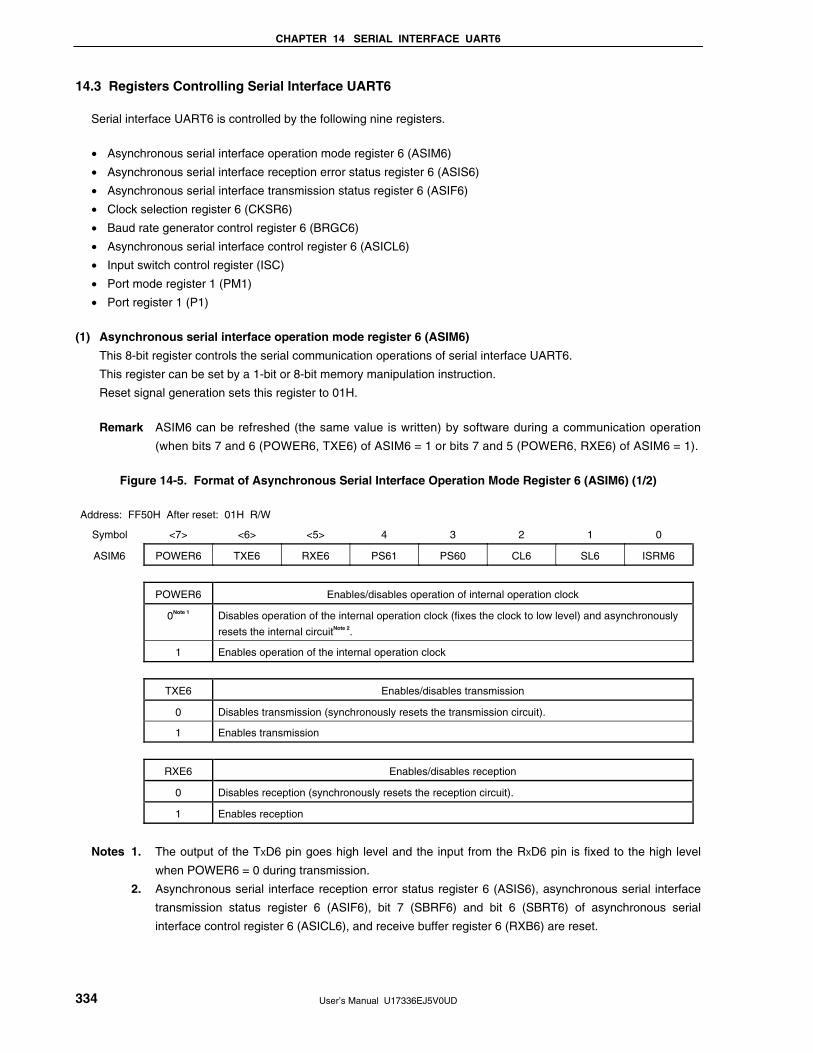
CHAPTER 14 SERIAL INTERFACE UART6
User’s Manual U17336EJ5V0UD 334
14.3 Registers Controlling Serial Interface UART6
Serial interface UART6 is controlled by the following nine registers.
• Asynchronous serial interface operation mode register 6 (ASIM6)
• Asynchronous serial interface reception error status register 6 (ASIS6)
• Asynchronous serial interface transmission status register 6 (ASIF6)
• Clock selection register 6 (CKSR6)
• Baud rate generator control register 6 (BRGC6)
• Asynchronous serial interface control register 6 (ASICL6)
• Input switch control register (ISC)
• Port mode register 1 (PM1)
• Port register 1 (P1)
(1) Asynchronous serial interface operation mode register 6 (ASIM6)
This 8-bit register controls the serial communication operations of serial interface UART6.
This register can be set by a 1-bit or 8-bit memory manipulation instruction.
Reset signal generation sets this register to 01H.
Remark ASIM6 can be refreshed (the same value is written) by software during a communication operation
(when bits 7 and 6 (POWER6, TXE6) of ASIM6 = 1 or bits 7 and 5 (POWER6, RXE6) of ASIM6 = 1).
Figure 14-5. Format of Asynchronous Serial Interface Operation Mode Register 6 (ASIM6) (1/2)
Address: FF50H After reset: 01H R/W
Symbol <7> <6> <5> 4 3 2 1 0
ASIM6 POWER6 TXE6 RXE6 PS61 PS60 CL6 SL6 ISRM6
POWER6 Enables/disables operation of internal operation clock
0Note 1 Disables operation of the internal operation clock (fixes the clock to low level) and asynchronously
resets the internal circuitNote 2.
1 Enables operation of the internal operation clock
TXE6 Enables/disables transmission
0 Disables transmission (synchronously resets the transmission circuit).
1 Enables transmission
RXE6 Enables/disables reception
0 Disables reception (synchronously resets the reception circuit).
1 Enables reception
Notes 1. The output of the TXD6 pin goes high level and the input from the RXD6 pin is fixed to the high level
when POWER6 = 0 during transmission.
2. Asynchronous serial interface reception error status register 6 (ASIS6), asynchronous serial interface
transmission status register 6 (ASIF6), bit 7 (SBRF6) and bit 6 (SBRT6) of asynchronous serial
interface control register 6 (ASICL6), and receive buffer register 6 (RXB6) are reset.

CHAPTER 14 SERIAL INTERFACE UART6
User’s Manual U17336EJ5V0UD 335
Figure 14-5. Format of Asynchronous Serial Interface Operation Mode Register 6 (ASIM6) (2/2)
PS61 PS60 Transmission operation Reception operation
0 0 Does not output parity bit. Reception without parity
0 1 Outputs 0 parity. Reception as 0 parityNote
1 0 Outputs odd parity. Judges as odd parity.
1 1 Outputs even parity. Judges as even parity.
CL6 Specifies character length of transmit/receive data
0 Character length of data = 7 bits
1 Character length of data = 8 bits
SL6 Specifies number of stop bits of transmit data
0 Number of stop bits = 1
1 Number of stop bits = 2
ISRM6 Enables/disables occurrence of reception completion interrupt in case of error
0 “INTSRE6” occurs in case of error (at this time, INTSR6 does not occur).
1 “INTSR6” occurs in case of error (at this time, INTSRE6 does not occur).
Note If “reception as 0 parity” is selected, the parity is not judged. Therefore, bit 2 (PE6) of asynchronous serial
interface reception error status register 6 (ASIS6) is not set and the error interrupt does not occur.
Cautions 1. To start the transmission, set POWER6 to 1 and then set TXE6 to 1. To stop the transmission,
clear TXE6 to 0, and then clear POWER6 to 0.
2. To start the reception, set POWER6 to 1 and then set RXE6 to 1. To stop the reception, clear
RXE6 to 0, and then clear POWER6 to 0.
3. Set POWER6 to 1 and then set RXE6 to 1 while a high level is input to the RXD6 pin. If
POWER6 is set to 1 and RXE6 is set to 1 while a low level is input, reception is started.
4. TXE6 and RXE6 are synchronized by the base clock (fXCLK6) set by CKSR6. To enable
transmission or reception again, set TXE6 or RXE6 to 1 at least two clocks of the base clock
after TXE6 or RXE6 has been cleared to 0. If TXE6 or RXE6 is set within two clocks of the
base clock, the transmission circuit or reception circuit may not be initialized.
5. Set transmit data to TXB6 at least one base clock (fXCLK6) after setting TXE6 = 1.
6. Clear the TXE6 and RXE6 bits to 0 before rewriting the PS61, PS60, and CL6 bits.
7. Fix the PS61 and PS60 bits to 0 when used in LIN communication operation.
8. Clear TXE6 to 0 before rewriting the SL6 bit. Reception is always performed with “the
number of stop bits = 1”, and therefore, is not affected by the set value of the SL6 bit.
9. Make sure that RXE6 = 0 when rewriting the ISRM6 bit.
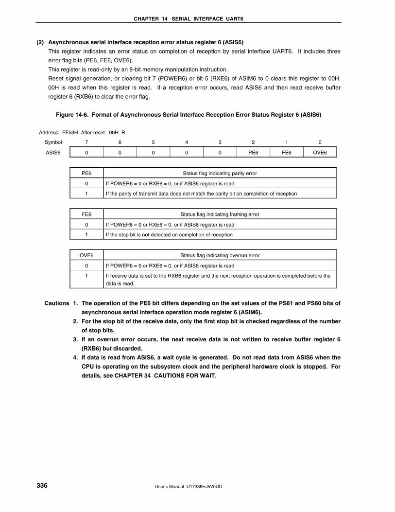
CHAPTER 14 SERIAL INTERFACE UART6
User’s Manual U17336EJ5V0UD 336
(2) Asynchronous serial interface reception error status register 6 (ASIS6)
This register indicates an error status on completion of reception by serial interface UART6. It includes three
error flag bits (PE6, FE6, OVE6).
This register is read-only by an 8-bit memory manipulation instruction.
Reset signal generation, or clearing bit 7 (POWER6) or bit 5 (RXE6) of ASIM6 to 0 clears this register to 00H.
00H is read when this register is read. If a reception error occurs, read ASIS6 and then read receive buffer
register 6 (RXB6) to clear the error flag.
Figure 14-6. Format of Asynchronous Serial Interface Reception Error Status Register 6 (ASIS6)
Address: FF53H After reset: 00H R
Symbol 7 6 5 4 3 2 1 0
ASIS6 0 0 0 0 0 PE6 FE6 OVE6
PE6 Status flag indicating parity error
0 If POWER6 = 0 or RXE6 = 0, or if ASIS6 register is read
1 If the parity of transmit data does not match the parity bit on completion of reception
FE6 Status flag indicating framing error
0 If POWER6 = 0 or RXE6 = 0, or if ASIS6 register is read
1 If the stop bit is not detected on completion of reception
OVE6 Status flag indicating overrun error
0 If POWER6 = 0 or RXE6 = 0, or if ASIS6 register is read
1 If receive data is set to the RXB6 register and the next reception operation is completed before the
data is read.
Cautions 1. The operation of the PE6 bit differs depending on the set values of the PS61 and PS60 bits of
asynchronous serial interface operation mode register 6 (ASIM6).
2. For the stop bit of the receive data, only the first stop bit is checked regardless of the number
of stop bits.
3. If an overrun error occurs, the next receive data is not written to receive buffer register 6
(RXB6) but discarded.
4. If data is read from ASIS6, a wait cycle is generated. Do not read data from ASIS6 when the
CPU is operating on the subsystem clock and the peripheral hardware clock is stopped. For
details, see CHAPTER 34 CAUTIONS FOR WAIT.

CHAPTER 14 SERIAL INTERFACE UART6
User’s Manual U17336EJ5V0UD 337
(3) Asynchronous serial interface transmission status register 6 (ASIF6)
This register indicates the status of transmission by serial interface UART6. It includes two status flag bits
(TXBF6 and TXSF6).
Transmission can be continued without disruption even during an interrupt period, by writing the next data to the
TXB6 register after data has been transferred from the TXB6 register to the TXS6 register.
This register is read-only by an 8-bit memory manipulation instruction.
Reset signal generation, or clearing bit 7 (POWER6) or bit 6 (TXE6) of ASIM6 to 0 clears this register to 00H.
Figure 14-7. Format of Asynchronous Serial Interface Transmission Status Register 6 (ASIF6)
Address: FF55H After reset: 00H R
Symbol 7 6 5 4 3 2 1 0
ASIF6 0 0 0 0 0 0 TXBF6 TXSF6
TXBF6 Transmit buffer data flag
0 If POWER6 = 0 or TXE6 = 0, or if data is transferred to transmit shift register 6 (TXS6)
1 If data is written to transmit buffer register 6 (TXB6) (if data exists in TXB6)
TXSF6 Transmit shift register data flag
0 If POWER6 = 0 or TXE6 = 0, or if the next data is not transferred from transmit buffer register 6
(TXB6) after completion of transfer
1 If data is transferred from transmit buffer register 6 (TXB6) (if data transmission is in progress)
Cautions 1. To transmit data continuously, write the first transmit data (first byte) to the TXB6 register.
Be sure to check that the TXBF6 flag is “0”. If so, write the next transmit data (second byte)
to the TXB6 register. If data is written to the TXB6 register while the TXBF6 flag is “1”, the
transmit data cannot be guaranteed.
2. To initialize the transmission unit upon completion of continuous transmission, be sure to
check that the TXSF6 flag is “0” after generation of the transmission completion interrupt,
and then execute initialization. If initialization is executed while the TXSF6 flag is “1”, the
transmit data cannot be guaranteed.
(4) Clock selection register 6 (CKSR6)
This register selects the base clock of serial interface UART6.
CKSR6 can be set by an 8-bit memory manipulation instruction.
Reset signal generation clears this register to 00H.
Remark CKSR6 can be refreshed (the same value is written) by software during a communication operation
(when bits 7 and 6 (POWER6, TXE6) of ASIM6 = 1 or bits 7 and 5 (POWER6, RXE6) of ASIM6 = 1).

CHAPTER 14 SERIAL INTERFACE UART6
User’s Manual U17336EJ5V0UD 338
Figure 14-8. Format of Clock Selection Register 6 (CKSR6)
Address: FF56H After reset: 00H R/W
Symbol 7 6 5 4 3 2 1 0
CKSR6 0 0 0 0 TPS63 TPS62 TPS61 TPS60
Base clock (fXCLK6) selectionNote 1 TPS63 TPS62 TPS61 TPS60
fPRS =
2 MHz
fPRS =
5 MHz
fPRS =
10 MHz
fPRS =
20 MHz
0 0 0 0 fPRSNote 2 2 MHz 5 MHz 10 MHz 20 MHz
0 0 0 1 fPRS/2 1 MHz 2.5 MHz 5 MHz 10 MHz
0 0 1 0 fPRS/22 500 kHz 1.25 MHz 2.5 MHz 5 MHz
0 0 1 1 fPRS/23 250 kHz 625 kHz 1.25 MHz 2.5 MHz
0 1 0 0 fPRS/24 125 kHz 312.5 kHz 625 kHz 1.25 MHz
0 1 0 1 fPRS/25 62.5 kHz 156.25 kHz 312.5 kHz 625 kHz
0 1 1 0 fPRS/26 31.25 kHz 78.13 kHz 156.25 kHz 312.5 kHz
0 1 1 1 fPRS/27 15.625 kHz 39.06 kHz 78.13 kHz 156.25 kHz
1 0 0 0 fPRS/28 7.813 kHz 19.53 kHz 39.06 kHz 78.13 kHz
1 0 0 1 fPRS/29 3.906 kHz 9.77 kHz 19.53 kHz 39.06 kHz
1 0 1 0 fPRS/210 1.953 kHz 4.88 kHz 9.77 kHz 19.53 kHz
1 0 1 1 TM50 outputNote 3
Other than above Setting prohibited
Notes 1. If the peripheral hardware clock (fPRS) operates on the high-speed system clock (fXH) (XSEL = 1), the
fPRS operating frequency varies depending on the supply voltage.
• VDD = 4.0 to 5.5 V: fPRS ≤ 20 MHz
• VDD = 2.7 to 4.0 V: fPRS ≤ 10 MHz
• VDD = 1.8 to 2.7 V: fPRS ≤ 5 MHz (Standard and (A) grade products only)
2. If the peripheral hardware clock (fPRS) operates on the internal high-speed oscillation clock (fRH) (XSEL
= 0), when 1.8 V ≤ VDD < 2.7 V, the setting of TPS63 = TPS62 = TPS61 = TPS60 = 0 (base clock: fPRS)
is prohibited.
3. Note the following points when selecting the TM50 output as the base clock.
• Mode in which the count clock is cleared and started upon a match of TM50 and CR50 (TMC506 =
0)
Start the operation of 8-bit timer/event counter 50 first and then enable the timer F/F inversion
operation (TMC501 = 1).
• PWM mode (TMC506 = 1)
Start the operation of 8-bit timer/event counter 50 first and then set the count clock to make the duty
= 50%.
It is not necessary to enable (TOE50 = 1) TO50 output in any mode.
Caution Make sure POWER6 = 0 when rewriting TPS63 to TPS60.
Remarks 1. fPRS: Peripheral hardware clock frequency
2. TMC506: Bit 6 of 8-bit timer mode control register 50 (TMC50)
TMC501: Bit 1 of TMC50
<R>
<R>
<R>

CHAPTER 14 SERIAL INTERFACE UART6
User’s Manual U17336EJ5V0UD 339
(5) Baud rate generator control register 6 (BRGC6)
This register sets the division value of the 8-bit counter of serial interface UART6.
BRGC6 can be set by an 8-bit memory manipulation instruction.
Reset signal generation sets this register to FFH.
Remark BRGC6 can be refreshed (the same value is written) by software during a communication operation
(when bits 7 and 6 (POWER6, TXE6) of ASIM6 = 1 or bits 7 and 5 (POWER6, RXE6) of ASIM6 = 1).
Figure 14-9. Format of Baud Rate Generator Control Register 6 (BRGC6)
Address: FF57H After reset: FFH R/W
Symbol 7 6 5 4 3 2 1 0
BRGC6 MDL67 MDL66 MDL65 MDL64 MDL63 MDL62 MDL61 MDL60
MDL67 MDL66 MDL65 MDL64 MDL63 MDL62 MDL61 MDL60 k Output clock selection of
8-bit counter
0 0 0 0 0 0 × × × Setting prohibited
0 0 0 0 0 1 0 0 4 fXCLK6/4
0 0 0 0 0 1 0 1 5 fXCLK6/5
0 0 0 0 0 1 1 0 6 fXCLK6/6
•
•
•
•
•
•
•
•
•
•
•
•
•
•
•
•
•
•
•
•
•
•
•
•
•
•
•
•
•
•
•
•
•
•
•
•
•
•
•
•
•
•
•
•
•
•
•
•
•
•
1 1 1 1 1 1 0 0 252 fXCLK6/252
1 1 1 1 1 1 0 1 253 fXCLK6/253
1 1 1 1 1 1 1 0 254 fXCLK6/254
1 1 1 1 1 1 1 1 255 fXCLK6/255
Cautions 1. Make sure that bit 6 (TXE6) and bit 5 (RXE6) of the ASIM6 register = 0 when rewriting the
MDL67 to MDL60 bits.
2. The baud rate is the output clock of the 8-bit counter divided by 2.
Remarks 1. fXCLK6: Frequency of base clock selected by the TPS63 to TPS60 bits of CKSR6 register
2. k: Value set by MDL67 to MDL60 bits (k = 4, 5, 6, ..., 255)
3. ×: Don’t care

CHAPTER 14 SERIAL INTERFACE UART6
User’s Manual U17336EJ5V0UD 340
(6) Asynchronous serial interface control register 6 (ASICL6)
This register controls the serial communication operations of serial interface UART6.
ASICL6 can be set by a 1-bit or 8-bit memory manipulation instruction.
Reset signal generation sets this register to 16H.
Caution ASICL6 can be refreshed (the same value is written) by software during a communication
operation (when bits 7 and 6 (POWER6, TXE6) of ASIM6 = 1 or bits 7 and 5 (POWER6, RXE6) of
ASIM6 = 1). However, do not set both SBRT6 and SBTT6 to 1 by a refresh operation during SBF
reception (SBRT6 = 1) or SBF transmission (until INTST6 occurs since SBTT6 has been set (1)),
because it may re-trigger SBF reception or SBF transmission.
Figure 14-10. Format of Asynchronous Serial Interface Control Register 6 (ASICL6) (1/2)
Address: FF58H After reset: 16H R/WNote
Symbol <7> <6> 5 4 3 2 1 0
ASICL6 SBRF6 SBRT6 SBTT6 SBL62 SBL61 SBL60 DIR6 TXDLV6
SBRF6 SBF reception status flag
0 If POWER6 = 0 and RXE6 = 0 or if SBF reception has been completed correctly
1 SBF reception in progress
SBRT6 SBF reception trigger
0 −
1 SBF reception trigger
SBTT6 SBF transmission trigger
0 −
1 SBF transmission trigger
Note Bit 7 is read-only.
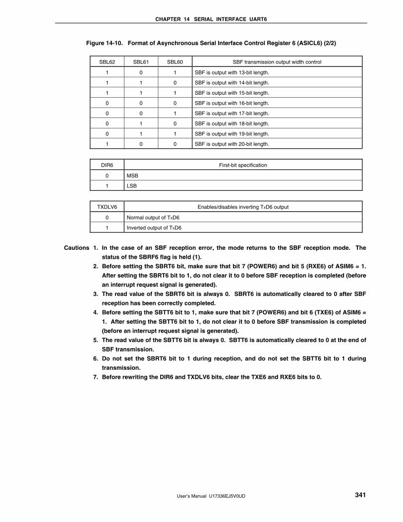
CHAPTER 14 SERIAL INTERFACE UART6
User’s Manual U17336EJ5V0UD 341
Figure 14-10. Format of Asynchronous Serial Interface Control Register 6 (ASICL6) (2/2)
SBL62 SBL61 SBL60 SBF transmission output width control
1 0 1 SBF is output with 13-bit length.
1 1 0 SBF is output with 14-bit length.
1 1 1 SBF is output with 15-bit length.
0 0 0 SBF is output with 16-bit length.
0 0 1 SBF is output with 17-bit length.
0 1 0 SBF is output with 18-bit length.
0 1 1 SBF is output with 19-bit length.
1 0 0 SBF is output with 20-bit length.
DIR6 First-bit specification
0 MSB
1 LSB
TXDLV6 Enables/disables inverting TXD6 output
0 Normal output of TXD6
1 Inverted output of TXD6
Cautions 1. In the case of an SBF reception error, the mode returns to the SBF reception mode. The
status of the SBRF6 flag is held (1).
2. Before setting the SBRT6 bit, make sure that bit 7 (POWER6) and bit 5 (RXE6) of ASIM6 = 1.
After setting the SBRT6 bit to 1, do not clear it to 0 before SBF reception is completed (before
an interrupt request signal is generated).
3. The read value of the SBRT6 bit is always 0. SBRT6 is automatically cleared to 0 after SBF
reception has been correctly completed.
4. Before setting the SBTT6 bit to 1, make sure that bit 7 (POWER6) and bit 6 (TXE6) of ASIM6 =
1. After setting the SBTT6 bit to 1, do not clear it to 0 before SBF transmission is completed
(before an interrupt request signal is generated).
5. The read value of the SBTT6 bit is always 0. SBTT6 is automatically cleared to 0 at the end of
SBF transmission.
6. Do not set the SBRT6 bit to 1 during reception, and do not set the SBTT6 bit to 1 during
transmission.
7. Before rewriting the DIR6 and TXDLV6 bits, clear the TXE6 and RXE6 bits to 0.

CHAPTER 14 SERIAL INTERFACE UART6
User’s Manual U17336EJ5V0UD 342
(7) Input switch control register (ISC)
The input switch control register (ISC) is used to receive a status signal transmitted from the master during LIN
(Local Interconnect Network) reception.
The signal input from the P14/RXD6 pin is selected as the input source of INTP0 and TI000 when ISC0 and ISC1
are set to 1.
This register can be set by a 1-bit or 8-bit memory manipulation instruction.
Reset signal generation clears this register to 00H.
Figure 14-11. Format of Input Switch Control Register (ISC)
Address: FF4FH After reset: 00H R/W
Symbol 7 6 5 4 3 2 1 0
ISC 0 0 0 0 0 0 ISC1 ISC0
ISC1 TI000 input source selection
0 TI000 (P00)
1 RXD6 (P14)
ISC0 INTP0 input source selection
0 INTP0 (P120)
1 RXD6 (P14)
(8) Port mode register 1 (PM1)
This register sets port 1 input/output in 1-bit units.
When using the P13/TXD6 pin for serial interface data output, clear PM13 to 0 and set the output latch of P13 to 1.
When using the P14/RXD6 pin for serial interface data input, set PM14 to 1. The output latch of P14 at this time
may be 0 or 1.
PM1 can be set by a 1-bit or 8-bit memory manipulation instruction.
Reset signal generation sets this register to FFH.
Figure 14-12. Format of Port Mode Register 1 (PM1)
Address: FF21H After reset: FFH R/W
Symbol 7 6 5 4 3 2 1 0
PM1 PM17 PM16 PM15 PM14 PM13 PM12 PM11 PM10
PM1n P1n pin I/O mode selection (n = 0 to 7)
0 Output mode (output buffer on)
1 Input mode (output buffer off)

CHAPTER 14 SERIAL INTERFACE UART6
User’s Manual U17336EJ5V0UD 343
14.4 Operation of Serial Interface UART6
Serial interface UART6 has the following two modes.
• Operation stop mode
• Asynchronous serial interface (UART) mode
14.4.1 Operation stop mode
In this mode, serial communication cannot be executed; therefore, the power consumption can be reduced. In
addition, the pins can be used as ordinary port pins in this mode. To set the operation stop mode, clear bits 7, 6, and
5 (POWER6, TXE6, and RXE6) of ASIM6 to 0.
(1) Register used
The operation stop mode is set by asynchronous serial interface operation mode register 6 (ASIM6).
ASIM6 can be set by a 1-bit or 8-bit memory manipulation instruction.
Reset signal generation sets this register to 01H.
Address: FF50H After reset: 01H R/W
Symbol <7> <6> <5> 4 3 2 1 0
ASIM6 POWER6 TXE6 RXE6 PS61 PS60 CL6 SL6 ISRM6
POWER6 Enables/disables operation of internal operation clock
0Note 1 Disables operation of the internal operation clock (fixes the clock to low level) and asynchronously
resets the internal circuitNote 2.
TXE6 Enables/disables transmission
0 Disables transmission operation (synchronously resets the transmission circuit).
RXE6 Enables/disables reception
0 Disables reception (synchronously resets the reception circuit).
Notes 1. The output of the TXD6 pin goes high and the input from the RXD6 pin is fixed to high level when
POWER6 = 0 during transmission.
2. Asynchronous serial interface reception error status register 6 (ASIS6), asynchronous serial interface
transmission status register 6 (ASIF6), bit 7 (SBRF6) and bit 6 (SBRT6) of asynchronous serial
interface control register 6 (ASICL6), and receive buffer register 6 (RXB6) are reset.
Caution Clear POWER6 to 0 after clearing TXE6 and RXE6 to 0 to stop the operation.
To start the communication, set POWER6 to 1, and then set TXE6 or RXE6 to 1.
Remark To use the RXD6/P14 and TXD6/P13 pins as general-purpose port pins, see CHAPTER 4 PORT
FUNCTIONS.

CHAPTER 14 SERIAL INTERFACE UART6
User’s Manual U17336EJ5V0UD 344
14.4.2 Asynchronous serial interface (UART) mode
In this mode, data of 1 byte is transmitted/received following a start bit, and a full-duplex operation can be
performed.
A dedicated UART baud rate generator is incorporated, so that communication can be executed at a wide range of
baud rates. (1) Registers used
• Asynchronous serial interface operation mode register 6 (ASIM6)
• Asynchronous serial interface reception error status register 6 (ASIS6)
• Asynchronous serial interface transmission status register 6 (ASIF6)
• Clock selection register 6 (CKSR6)
• Baud rate generator control register 6 (BRGC6)
• Asynchronous serial interface control register 6 (ASICL6)
• Input switch control register (ISC)
• Port mode register 1 (PM1)
• Port register 1 (P1)
The basic procedure of setting an operation in the UART mode is as follows.
<1> Set the CKSR6 register (see Figure 14-8).
<2> Set the BRGC6 register (see Figure 14-9).
<3> Set bits 0 to 4 (ISRM6, SL6, CL6, PS60, PS61) of the ASIM6 register (see Figure 14-5).
<4> Set bits 0 and 1 (TXDLV6, DIR6) of the ASICL6 register (see Figure 14-10).
<5> Set bit 7 (POWER6) of the ASIM6 register to 1.
<6> Set bit 6 (TXE6) of the ASIM6 register to 1. → Transmission is enabled.
Set bit 5 (RXE6) of the ASIM6 register to 1. → Reception is enabled.
<7> Write data to transmit buffer register 6 (TXB6). → Data transmission is started.
Caution Take the relationship with the other party of communication when setting the port mode
register and port register.
The relationship between the register settings and pins is shown below.
Table 14-2. Relationship Between Register Settings and Pins
Pin Function POWER6 TXE6 RXE6 PM13 P13 PM14 P14 UART6 Operation TXD6/P13 RXD6/P14
0 0 0 ×Note ×Note ×Note ×Note Stop P13 P14
0 1 ×Note ×Note 1 × Reception P13 RXD6
1 0 0 1 ×Note ×Note Transmission TXD6 P14
1
1 1 0 1 1 × Transmission/reception
TXD6 RXD6
Note Can be set as port function.
Remark ×: don’t care
POWER6: Bit 7 of asynchronous serial interface operation mode register 6 (ASIM6)
TXE6: Bit 6 of ASIM6
RXE6: Bit 5 of ASIM6
PM1×: Port mode register
P1×: Port output latch

CHAPTER 14 SERIAL INTERFACE UART6
User’s Manual U17336EJ5V0UD 345
(2) Communication operation
(a) Format and waveform example of normal transmit/receive data
Figures 14-13 and 14-14 show the format and waveform example of the normal transmit/receive data.
Figure 14-13. Format of Normal UART Transmit/Receive Data
1. LSB-first transmission/reception
Start bit
Parity bit
D0 D1 D2 D3 D4
1 data frame
Character bits
D5 D6 D7 Stop bit
2. MSB-first transmission/reception
Start bit
Parity bit
D7 D6 D5 D4 D3
1 data frame
Character bits
D2 D1 D0 Stop bit
One data frame consists of the following bits.
• Start bit ... 1 bit
• Character bits ... 7 or 8 bits
• Parity bit ... Even parity, odd parity, 0 parity, or no parity
• Stop bit ... 1 or 2 bits
The character bit length, parity, and stop bit length in one data frame are specified by asynchronous serial
interface operation mode register 6 (ASIM6).
Whether data is communicated with the LSB or MSB first is specified by bit 1 (DIR6) of asynchronous serial
interface control register 6 (ASICL6).
Whether the TXD6 pin outputs normal or inverted data is specified by bit 0 (TXDLV6) of ASICL6.
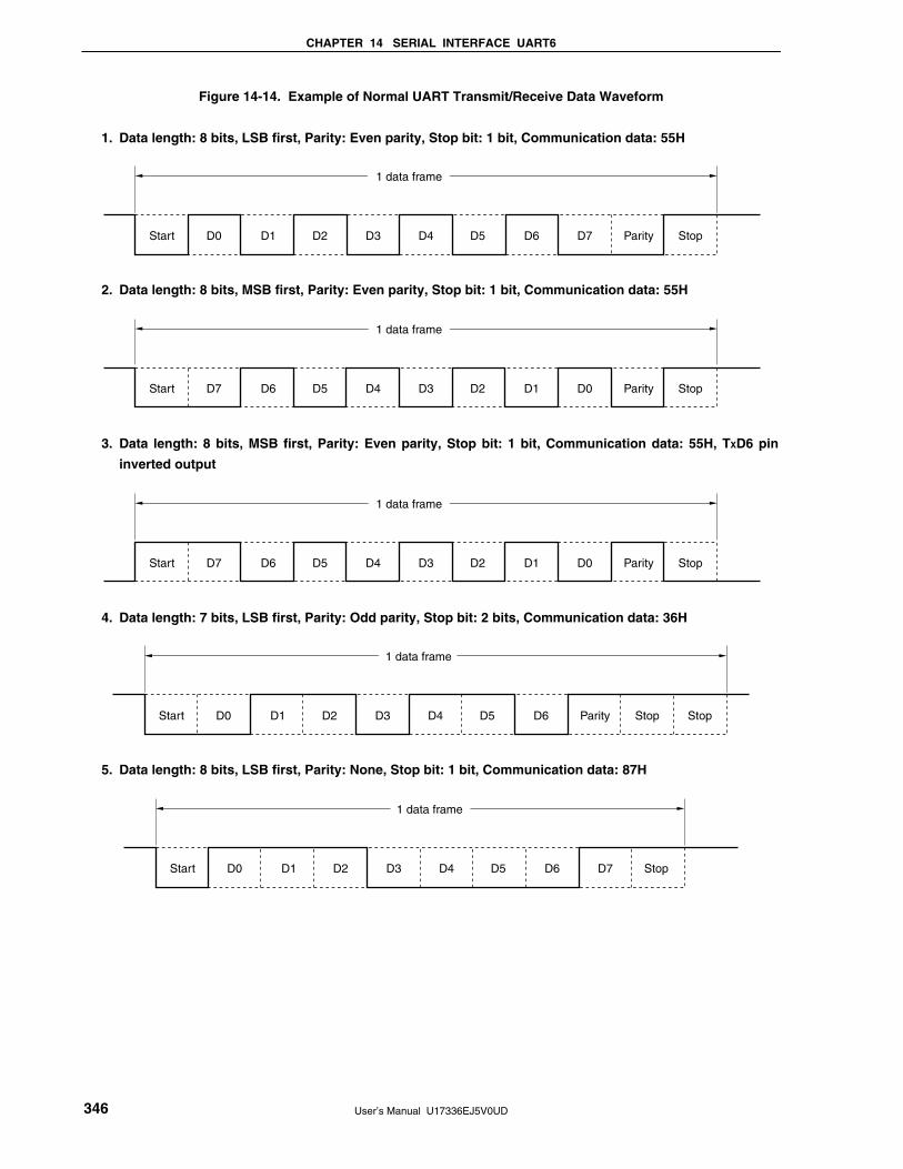
CHAPTER 14 SERIAL INTERFACE UART6
User’s Manual U17336EJ5V0UD 346
Figure 14-14. Example of Normal UART Transmit/Receive Data Waveform
1. Data length: 8 bits, LSB first, Parity: Even parity, Stop bit: 1 bit, Communication data: 55H
1 data frame
Start D0 D1 D2 D3 D4 D5 D6 D7 Parity Stop
2. Data length: 8 bits, MSB first, Parity: Even parity, Stop bit: 1 bit, Communication data: 55H
1 data frame
Start D7 D6 D5 D4 D3 D2 D1 D0 Parity Stop
3. Data length: 8 bits, MSB first, Parity: Even parity, Stop bit: 1 bit, Communication data: 55H, TXD6 pin
inverted output
1 data frame
Start D7 D6 D5 D4 D3 D2 D1 D0 Parity Stop
4. Data length: 7 bits, LSB first, Parity: Odd parity, Stop bit: 2 bits, Communication data: 36H
1 data frame
Start D0 D1 D2 D3 D4 D5 D6 Parity StopStop
5. Data length: 8 bits, LSB first, Parity: None, Stop bit: 1 bit, Communication data: 87H
1 data frame
Start D0 D1 D2 D3 D4 D5 D6 D7 Stop

CHAPTER 14 SERIAL INTERFACE UART6
User’s Manual U17336EJ5V0UD 347
(b) Parity types and operation
The parity bit is used to detect a bit error in communication data. Usually, the same type of parity bit is used
on both the transmission and reception sides. With even parity and odd parity, a 1-bit (odd number) error
can be detected. With zero parity and no parity, an error cannot be detected.
Caution Fix the PS61 and PS60 bits to 0 when the device is used in LIN communication operation.
(i) Even parity
• Transmission
Transmit data, including the parity bit, is controlled so that the number of bits that are “1” is even.
The value of the parity bit is as follows.
If transmit data has an odd number of bits that are “1”: 1
If transmit data has an even number of bits that are “1”: 0
• Reception
The number of bits that are “1” in the receive data, including the parity bit, is counted. If it is odd, a
parity error occurs.
(ii) Odd parity
• Transmission
Unlike even parity, transmit data, including the parity bit, is controlled so that the number of bits that
are “1” is odd.
If transmit data has an odd number of bits that are “1”: 0
If transmit data has an even number of bits that are “1”: 1
• Reception
The number of bits that are “1” in the receive data, including the parity bit, is counted. If it is even, a
parity error occurs.
(iii) 0 parity
The parity bit is cleared to 0 when data is transmitted, regardless of the transmit data.
The parity bit is not detected when the data is received. Therefore, a parity error does not occur
regardless of whether the parity bit is “0” or “1”.
(iv) No parity
No parity bit is appended to the transmit data.
Reception is performed assuming that there is no parity bit when data is received. Because there is no
parity bit, a parity error does not occur.

CHAPTER 14 SERIAL INTERFACE UART6
User’s Manual U17336EJ5V0UD 348
(c) Normal transmission
When bit 7 (POWER6) of asynchronous serial interface operation mode register 6 (ASIM6) is set to 1 and bit
6 (TXE6) of ASIM6 is then set to 1, transmission is enabled. Transmission can be started by writing transmit
data to transmit buffer register 6 (TXB6). The start bit, parity bit, and stop bit are automatically appended to
the data.
When transmission is started, the data in TXB6 is transferred to transmit shift register 6 (TXS6). After that,
the transmit data is sequentially output from TXS6 to the TXD6 pin. When transmission is completed, the
parity and stop bits set by ASIM6 are appended and a transmission completion interrupt request (INTST6) is
generated.
Transmission is stopped until the data to be transmitted next is written to TXB6.
Figure 14-15 shows the timing of the transmission completion interrupt request (INTST6). This interrupt
occurs as soon as the last stop bit has been output.
Figure 14-15. Normal Transmission Completion Interrupt Request Timing
1. Stop bit length: 1
INTST6
D0Start D1 D2 D6 D7 StopTXD6 (output) Parity
2. Stop bit length: 2
TXD6 (output)
INTST6
D0Start D1 D2 D6 D7 Parity Stop

CHAPTER 14 SERIAL INTERFACE UART6
User’s Manual U17336EJ5V0UD 349
(d) Continuous transmission
The next transmit data can be written to transmit buffer register 6 (TXB6) as soon as transmit shift register 6
(TXS6) has started its shift operation. Consequently, even while the INTST6 interrupt is being serviced after
transmission of one data frame, data can be continuously transmitted and an efficient communication rate
can be realized. In addition, the TXB6 register can be efficiently written twice (2 bytes) without having to wait
for the transmission time of one data frame, by reading bit 0 (TXSF6) of asynchronous serial interface
transmission status register 6 (ASIF6) when the transmission completion interrupt has occurred.
To transmit data continuously, be sure to reference the ASIF6 register to check the transmission status and
whether the TXB6 register can be written, and then write the data.
Cautions 1. The TXBF6 and TXSF6 flags of the ASIF6 register change from “10” to “11”, and to “01”
during continuous transmission. To check the status, therefore, do not use a
combination of the TXBF6 and TXSF6 flags for judgment. Read only the TXBF6 flag
when executing continuous transmission.
2. When the device is use in LIN communication operation, the continuous transmission
function cannot be used. Make sure that asynchronous serial interface transmission
status register 6 (ASIF6) is 00H before writing transmit data to transmit buffer register 6
(TXB6).
TXBF6 Writing to TXB6 Register
0 Writing enabled
1 Writing disabled
Caution To transmit data continuously, write the first transmit data (first byte) to the TXB6 register.
Be sure to check that the TXBF6 flag is “0”. If so, write the next transmit data (second byte)
to the TXB6 register. If data is written to the TXB6 register while the TXBF6 flag is “1”, the
transmit data cannot be guaranteed.
The communication status can be checked using the TXSF6 flag.
TXSF6 Transmission Status
0 Transmission is completed.
1 Transmission is in progress.
Cautions 1. To initialize the transmission unit upon completion of continuous transmission, be sure
to check that the TXSF6 flag is “0” after generation of the transmission completion
interrupt, and then execute initialization. If initialization is executed while the TXSF6
flag is “1”, the transmit data cannot be guaranteed.
2. During continuous transmission, the next transmission may complete before execution
of INTST6 interrupt servicing after transmission of one data frame. As a
countermeasure, detection can be performed by developing a program that can count
the number of transmit data and by referencing the TXSF6 flag.

CHAPTER 14 SERIAL INTERFACE UART6
User’s Manual U17336EJ5V0UD 350
Figure 14-16 shows an example of the continuous transmission processing flow.
Figure 14-16. Example of Continuous Transmission Processing Flow
Write TXB6.
Set registers.
Write TXB6.
Transferexecuted necessary
number of times?Yes
Read ASIF6TXBF6 = 0?
No
No
Yes
Transmissioncompletion interrupt
occurs?
Read ASIF6TXSF6 = 0?
No
No
No
Yes
Yes
Yes
YesCompletion oftransmission processing
Transferexecuted necessary
number of times?
Remark TXB6: Transmit buffer register 6
ASIF6: Asynchronous serial interface transmission status register 6
TXBF6: Bit 1 of ASIF6 (transmit buffer data flag)
TXSF6: Bit 0 of ASIF6 (transmit shift register data flag)

CHAPTER 14 SERIAL INTERFACE UART6
User’s Manual U17336EJ5V0UD 351
Figure 14-17 shows the timing of starting continuous transmission, and Figure 14-18 shows the timing of
ending continuous transmission.
Figure 14-17. Timing of Starting Continuous Transmission
TXD6 Start
INTST6
Data (1)
Data (1) Data (2) Data (3)
Data (2)Data (1) Data (3)
FF
FF
Parity Stop Data (2) Parity Stop
TXB6
TXS6
TXBF6
TXSF6
Start Start
Note
Note When ASIF6 is read, there is a period in which TXBF6 and TXSF6 = 1, 1. Therefore, judge whether
writing is enabled using only the TXBF6 bit.
Remark TXD6: TXD6 pin (output)
INTST6: Interrupt request signal
TXB6: Transmit buffer register 6
TXS6: Transmit shift register 6
ASIF6: Asynchronous serial interface transmission status register 6
TXBF6: Bit 1 of ASIF6
TXSF6: Bit 0 of ASIF6

CHAPTER 14 SERIAL INTERFACE UART6
User’s Manual U17336EJ5V0UD 352
Figure 14-18. Timing of Ending Continuous Transmission
TXD6 Start
INTST6
Data (n − 1)
Data (n − 1) Data (n)
Data (n)Data (n − 1) FF
ParityStop Stop Data (n) Parity Stop
TXB6
TXS6
TXBF6
TXSF6
POWER6 or TXE6
Start
Remark TXD6: TXD6 pin (output)
INTST6: Interrupt request signal
TXB6: Transmit buffer register 6
TXS6: Transmit shift register 6
ASIF6: Asynchronous serial interface transmission status register 6
TXBF6: Bit 1 of ASIF6
TXSF6: Bit 0 of ASIF6
POWER6: Bit 7 of asynchronous serial interface operation mode register (ASIM6)
TXE6: Bit 6 of asynchronous serial interface operation mode register (ASIM6)

CHAPTER 14 SERIAL INTERFACE UART6
User’s Manual U17336EJ5V0UD 353
(e) Normal reception
Reception is enabled and the RXD6 pin input is sampled when bit 7 (POWER6) of asynchronous serial
interface operation mode register 6 (ASIM6) is set to 1 and then bit 5 (RXE6) of ASIM6 is set to 1.
The 8-bit counter of the baud rate generator starts counting when the falling edge of the RXD6 pin input is
detected. When the set value of baud rate generator control register 6 (BRGC6) has been counted, the
RXD6 pin input is sampled again ( in Figure 14-19). If the RXD6 pin is low level at this time, it is recognized
as a start bit.
When the start bit is detected, reception is started, and serial data is sequentially stored in the receive shift
register (RXS6) at the set baud rate. When the stop bit has been received, the reception completion interrupt
(INTSR6) is generated and the data of RXS6 is written to receive buffer register 6 (RXB6). If an overrun
error (OVE6) occurs, however, the receive data is not written to RXB6.
Even if a parity error (PE6) occurs while reception is in progress, reception continues to the reception
position of the stop bit, and a reception error interrupt (INTSR6/INTSRE6) is generated on completion of
reception.
Figure 14-19. Reception Completion Interrupt Request Timing
RXD6 (input)
INTSR6
Start D0 D1 D2 D3 D4 D5 D6 D7 Parity
RXB6
Stop
Cautions 1. If a reception error occurs, read ASIS6 and then RXB6 to clear the error flag. Otherwise,
an overrun error will occur when the next data is received, and the reception error
status will persist.
2. Reception is always performed with the “number of stop bits = 1”. The second stop bit
is ignored.
3. Be sure to read asynchronous serial interface reception error status register 6 (ASIS6)
before reading RXB6.

CHAPTER 14 SERIAL INTERFACE UART6
User’s Manual U17336EJ5V0UD 354
(f) Reception error
Three types of errors may occur during reception: a parity error, framing error, or overrun error. If the error
flag of asynchronous serial interface reception error status register 6 (ASIS6) is set as a result of data
reception, a reception error interrupt request (INTSR6/INTSRE6) is generated.
Which error has occurred during reception can be identified by reading the contents of ASIS6 in the reception
error interrupt (INTSR6/INTSRE6) servicing (see Figure 14-6).
The contents of ASIS6 are cleared to 0 when ASIS6 is read.
Table 14-3. Cause of Reception Error
Reception Error Cause
Parity error The parity specified for transmission does not match the parity of the receive data.
Framing error Stop bit is not detected.
Overrun error Reception of the next data is completed before data is read from receive buffer
register 6 (RXB6).
The reception error interrupt can be separated into reception completion interrupt (INTSR6) and error
interrupt (INTSRE6) by clearing bit 0 (ISRM6) of asynchronous serial interface operation mode register 6
(ASIM6) to 0.
Figure 14-20. Reception Error Interrupt
1. If ISRM6 is cleared to 0 (reception completion interrupt (INTSR6) and error interrupt (INTSRE6) are
separated)
(a) No error during reception (b) Error during reception
INTSR6
INTSRE6
INTSR6
INTSRE6
2. If ISRM6 is set to 1 (error interrupt is included in INTSR6)
(a) No error during reception (b) Error during reception
INTSRE6
INTSR6
INTSRE6
INTSR6

CHAPTER 14 SERIAL INTERFACE UART6
User’s Manual U17336EJ5V0UD 355
(g) Noise filter of receive data
The RxD6 signal is sampled with the base clock output by the prescaler block.
If two sampled values are the same, the output of the match detector changes, and the data is sampled as
input data.
Because the circuit is configured as shown in Figure 14-21, the internal processing of the reception operation
is delayed by two clocks from the external signal status.
Figure 14-21. Noise Filter Circuit
Internal signal BInternal signal A
Match detector
In
Base clock
RXD6/P14 Q In
LD_EN
Q
(h) SBF transmission
When the device is use in LIN communication operation, the SBF (Synchronous Break Field) transmission
control function is used for transmission. For the transmission operation of LIN, see Figure 14-1 LIN
Transmission Operation.
When bit 7 (POWER6) of asynchronous serial interface mode register 6 (ASIM6) is set to 1, the TXD6 pin
outputs high level. Next, when bit 6 (TXE6) of ASIM6 is set to 1, the transmission enabled status is entered,
and SBF transmission is started by setting bit 5 (SBTT6) of asynchronous serial interface control register 6
(ASICL6) to 1.
Thereafter, a low level of bits 13 to 20 (set by bits 4 to 2 (SBL62 to SBL60) of ASICL6) is output. Following
the end of SBF transmission, the transmission completion interrupt request (INTST6) is generated and
SBTT6 is automatically cleared. Thereafter, the normal transmission mode is restored.
Transmission is suspended until the data to be transmitted next is written to transmit buffer register 6 (TXB6),
or until SBTT6 is set to 1.
Figure 14-22. SBF Transmission
TXD6
INTST6
SBTT6
1 2 3 4 5 6 7 8 9 10 11 12 13 Stop
Remark TXD6: TXD6 pin (output)
INTST6: Transmission completion interrupt request
SBTT6: Bit 5 of asynchronous serial interface control register 6 (ASICL6)


CHAPTER 14 SERIAL INTERFACE UART6
User’s Manual U17336EJ5V0UD 357
14.4.3 Dedicated baud rate generator
The dedicated baud rate generator consists of a source clock selector and an 8-bit programmable counter, and
generates a serial clock for transmission/reception of UART6.
Separate 8-bit counters are provided for transmission and reception.
(1) Configuration of baud rate generator
• Base clock
The clock selected by bits 3 to 0 (TPS63 to TPS60) of clock selection register 6 (CKSR6) is supplied to
each module when bit 7 (POWER6) of asynchronous serial interface operation mode register 6 (ASIM6) is
1. This clock is called the base clock and its frequency is called fXCLK6. The base clock is fixed to low level
when POWER6 = 0.
• Transmission counter
This counter stops operation, cleared to 0, when bit 7 (POWER6) or bit 6 (TXE6) of asynchronous serial
interface operation mode register 6 (ASIM6) is 0.
It starts counting when POWER6 = 1 and TXE6 = 1.
The counter is cleared to 0 when the first data transmitted is written to transmit buffer register 6 (TXB6).
If data are continuously transmitted, the counter is cleared to 0 again when one frame of data has been
completely transmitted. If there is no data to be transmitted next, the counter is not cleared to 0 and continues
counting until POWER6 or TXE6 is cleared to 0.
• Reception counter
This counter stops operation, cleared to 0, when bit 7 (POWER6) or bit 5 (RXE6) of asynchronous serial
interface operation mode register 6 (ASIM6) is 0.
It starts counting when the start bit has been detected.
The counter stops operation after one frame has been received, until the next start bit is detected.
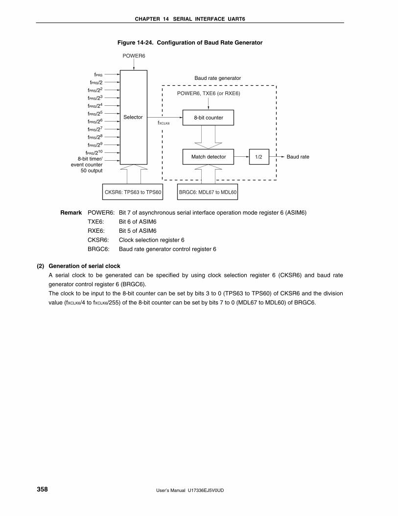
CHAPTER 14 SERIAL INTERFACE UART6
User’s Manual U17336EJ5V0UD 358
Figure 14-24. Configuration of Baud Rate Generator
Selector
POWER6
8-bit counter
Match detector Baud rate
Baud rate generator
BRGC6: MDL67 to MDL60
1/2
POWER6, TXE6 (or RXE6)
CKSR6: TPS63 to TPS60
fPRS
fPRS/2
fPRS/22
fPRS/23
fPRS/24
fPRS/25
fPRS/26
fPRS/27
fPRS/28
fPRS/29
fPRS/210
8-bit timer/event counter
50 output
fXCLK6
Remark POWER6: Bit 7 of asynchronous serial interface operation mode register 6 (ASIM6)
TXE6: Bit 6 of ASIM6
RXE6: Bit 5 of ASIM6
CKSR6: Clock selection register 6
BRGC6: Baud rate generator control register 6
(2) Generation of serial clock
A serial clock to be generated can be specified by using clock selection register 6 (CKSR6) and baud rate
generator control register 6 (BRGC6).
The clock to be input to the 8-bit counter can be set by bits 3 to 0 (TPS63 to TPS60) of CKSR6 and the division
value (fXCLK6/4 to fXCLK6/255) of the 8-bit counter can be set by bits 7 to 0 (MDL67 to MDL60) of BRGC6.
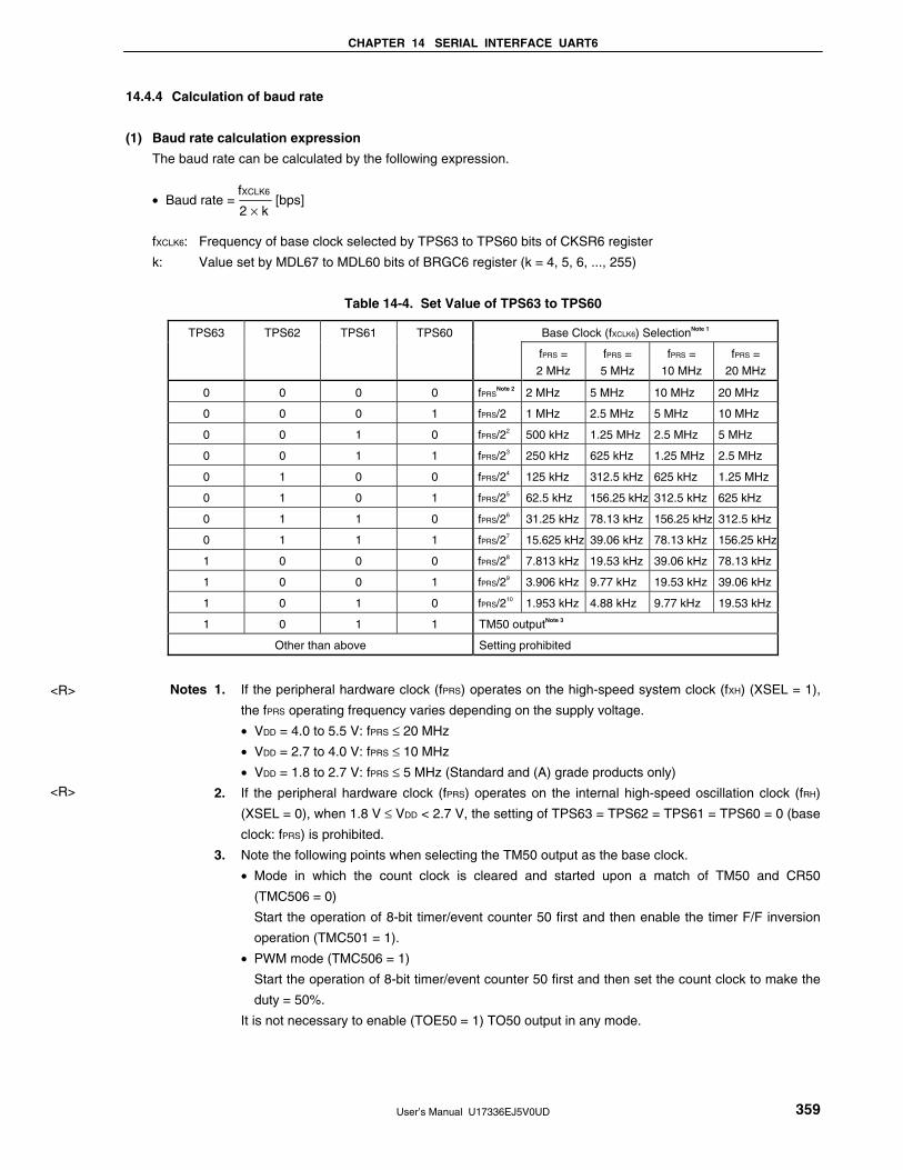
CHAPTER 14 SERIAL INTERFACE UART6
User’s Manual U17336EJ5V0UD 359
14.4.4 Calculation of baud rate
(1) Baud rate calculation expression
The baud rate can be calculated by the following expression.
• Baud rate = [bps]
fXCLK6: Frequency of base clock selected by TPS63 to TPS60 bits of CKSR6 register
k: Value set by MDL67 to MDL60 bits of BRGC6 register (k = 4, 5, 6, ..., 255)
Table 14-4. Set Value of TPS63 to TPS60
Base Clock (fXCLK6) SelectionNote 1 TPS63 TPS62 TPS61 TPS60
fPRS = 2 MHz
fPRS = 5 MHz
fPRS = 10 MHz
fPRS = 20 MHz
0 0 0 0 fPRSNote 2 2 MHz 5 MHz 10 MHz 20 MHz
0 0 0 1 fPRS/2 1 MHz 2.5 MHz 5 MHz 10 MHz
0 0 1 0 fPRS/22 500 kHz 1.25 MHz 2.5 MHz 5 MHz
0 0 1 1 fPRS/23 250 kHz 625 kHz 1.25 MHz 2.5 MHz
0 1 0 0 fPRS/24 125 kHz 312.5 kHz 625 kHz 1.25 MHz
0 1 0 1 fPRS/25 62.5 kHz 156.25 kHz 312.5 kHz 625 kHz
0 1 1 0 fPRS/26 31.25 kHz 78.13 kHz 156.25 kHz 312.5 kHz
0 1 1 1 fPRS/27 15.625 kHz 39.06 kHz 78.13 kHz 156.25 kHz
1 0 0 0 fPRS/28 7.813 kHz 19.53 kHz 39.06 kHz 78.13 kHz
1 0 0 1 fPRS/29 3.906 kHz 9.77 kHz 19.53 kHz 39.06 kHz
1 0 1 0 fPRS/210 1.953 kHz 4.88 kHz 9.77 kHz 19.53 kHz
1 0 1 1 TM50 outputNote 3
Other than above Setting prohibited
Notes 1. If the peripheral hardware clock (fPRS) operates on the high-speed system clock (fXH) (XSEL = 1),
the fPRS operating frequency varies depending on the supply voltage.
• VDD = 4.0 to 5.5 V: fPRS ≤ 20 MHz
• VDD = 2.7 to 4.0 V: fPRS ≤ 10 MHz
• VDD = 1.8 to 2.7 V: fPRS ≤ 5 MHz (Standard and (A) grade products only)
2. If the peripheral hardware clock (fPRS) operates on the internal high-speed oscillation clock (fRH)
(XSEL = 0), when 1.8 V ≤ VDD < 2.7 V, the setting of TPS63 = TPS62 = TPS61 = TPS60 = 0 (base
clock: fPRS) is prohibited.
3. Note the following points when selecting the TM50 output as the base clock.
• Mode in which the count clock is cleared and started upon a match of TM50 and CR50
(TMC506 = 0)
Start the operation of 8-bit timer/event counter 50 first and then enable the timer F/F inversion
operation (TMC501 = 1).
• PWM mode (TMC506 = 1)
Start the operation of 8-bit timer/event counter 50 first and then set the count clock to make the
duty = 50%.
It is not necessary to enable (TOE50 = 1) TO50 output in any mode.
fXCLK6
2 × k
<R>
<R>

CHAPTER 14 SERIAL INTERFACE UART6
User’s Manual U17336EJ5V0UD 360
(2) Error of baud rate
The baud rate error can be calculated by the following expression.
• Error (%) = − 1 × 100 [%]
Cautions 1. Keep the baud rate error during transmission to within the permissible error range at the
reception destination.
2. Make sure that the baud rate error during reception satisfies the range shown in (4)
Permissible baud rate range during reception.
Example: Frequency of base clock = 10 MHz = 10,000,000 Hz
Set value of MDL67 to MDL60 bits of BRGC6 register = 00100001B (k = 33)
Target baud rate = 153600 bps
Baud rate = 10 M / (2 × 33)
= 10000000 / (2 × 33) = 151,515 [bps]
Error = (151515/153600 − 1) × 100
= −1.357 [%]
(3) Example of setting baud rate
Table 14-5. Set Data of Baud Rate Generator
fPRS = 2.0 MHz fPRS = 5.0 MHz fPRS = 10.0 MHz fPRS = 20.0 MHz Baud
Rate
[bps] TPS63-
TPS60
k Calculated
Value
ERR
[%]
TPS63-
TPS60
k Calculated
Value
ERR
[%]
TPS63-
TPS60
k Calculated
Value
ERR
[%]
TPS63-
TPS60
k Calculated
Value
ERR
[%]
300 8H 13 301 0.16 7H 65 301 0.16 8H 65 301 0.16 9H 65 301 0.16
600 7H 13 601 0.16 6H 65 601 0.16 7H 65 601 0.16 8H 65 601 0.16
1200 6H 13 1202 0.16 5H 65 1202 0.16 6H 65 1202 0.16 7H 65 1202 0.16
2400 5H 13 2404 0.16 4H 65 2404 0.16 5H 65 2404 0.16 6H 65 2404 0.16
4800 4H 13 4808 0.16 3H 65 4808 0.16 4H 65 4808 0.16 5H 65 4808 0.16
9600 3H 13 9615 0.16 2H 65 9615 0.16 3H 65 9615 0.16 4H 65 9615 0.16
19200 2H 13 19231 0.16 1H 65 19231 0.16 2H 65 19231 0.16 3H 65 19231 0.16
24000 1H 21 23810

CHAPTER 14 SERIAL INTERFACE UART6
User’s Manual U17336EJ5V0UD 361
(4) Permissible baud rate range during reception
The permissible error from the baud rate at the transmission destination during reception is shown below.
Caution Make sure that the baud rate error during reception is within the permissible error range, by
using the calculation expression shown below.
Figure 14-25. Permissible Baud Rate Range During Reception
FL
1 data frame (11 × FL)
FLmin
FLmax
Data frame lengthof UART6
Start bit Bit 0 Bit 1 Bit 7 Parity bit
Minimum permissibledata frame length
Maximum permissibledata frame length
Stop bit
Start bit Bit 0 Bit 1 Bit 7 Parity bit
Latch timing
Stop bit
Start bit Bit 0 Bit 1 Bit 7 Parity bit Stop bit
As shown in Figure 14-25, the latch timing of the receive data is determined by the counter set by baud rate
generator control register 6 (BRGC6) after the start bit has been detected. If the last data (stop bit) meets this
latch timing, the data can be correctly received.
Assuming that 11-bit data is received, the theoretical values can be calculated as follows.
FL = (Brate)−1
Brate: Baud rate of UART6
k: Set value of BRGC6
FL: 1-bit data length
Margin of latch timing: 2 clocks

CHAPTER 14 SERIAL INTERFACE UART6
User’s Manual U17336EJ5V0UD 362
Minimum permissible data frame length: FLmin = 11 × FL − × FL = FL
Therefore, the maximum receivable baud rate at the transmission destination is as follows.
BRmax = (FLmin/11)−1 = Brate
Similarly, the maximum permissible data frame length can be calculated as follows.
10 k + 2 21k − 2
11 2 × k 2 × k
FLmax = FL × 11
Therefore, the minimum receivable baud rate at the transmission destination is as follows.
BRmin = (FLmax/11)−1 = Brate
The permissible baud rate error between UART6 and the transmission destination can be calculated from the
above minimum and maximum baud rate expressions, as follows.
Table 14-6. Maximum/Minimum Permissible Baud Rate Error
Division Ratio (k) Maximum Permissible Baud Rate Error Minimum Permissible Baud Rate Error
4 +2.33% −2.44%
8 +3.53% −3.61%
20 +4.26% −4.31%
50 +4.56% −4.58%
100 +4.66% −4.67%
255 +4.72% −4.73%
Remarks 1. The permissible error of reception depends on the number of bits in one frame, input clock
frequency, and division ratio (k). The higher the input clock frequency and the higher the division
ratio (k), the higher the permissible error.
2. k: Set value of BRGC6
22k
21k + 2
× FLmax = 11 × FL − × FL = FL
21k – 2
20k
20k
21k − 2
k − 2
2k
21k + 2
2k

CHAPTER 14 SERIAL INTERFACE UART6
User’s Manual U17336EJ5V0UD 363
(5) Data frame length during continuous transmission
When data is continuously transmitted, the data frame length from a stop bit to the next start bit is extended by
two clocks of base clock from the normal value. However, the result of communication is not affected because
the timing is initialized on the reception side when the start bit is detected.
Figure 14-26. Data Frame Length During Continuous Transmission
Start bit Bit 0 Bit 1 Bit 7 Parity bit Stop bit
FL
1 data frame
FL FL FL FL FLFLFLstp
Start bit of second byte
Start bit Bit 0
Where the 1-bit data length is FL, the stop bit length is FLstp, and base clock frequency is fXCLK6, the following
expression is satisfied.
FLstp = FL + 2/fXCLK6
Therefore, the data frame length during continuous transmission is:
Data frame length = 11 × FL + 2/fXCLK6

User’s Manual U17336EJ5V0UD 364
CHAPTER 15 SERIAL INTERFACE CSI10
15.1 Functions of Serial Interface CSI10
Serial interface CSI10 has the following two modes.
• Operation stop mode
• 3-wire serial I/O mode
(1) Operation stop mode
This mode is used when serial communication is not performed and can enable a reduction in the power
consumption.
For details, see 15.4.1 Operation stop mode.
(2) 3-wire serial I/O mode (MSB/LSB-first selectable)
This mode is used to communicate 8-bit data using three lines: a serial clock line (SCK10) and two serial data
lines (SI10 and SO10).
The processing time of data communication can be shortened in the 3-wire serial I/O mode because transmission
and reception can be simultaneously executed.
In addition, whether 8-bit data is communicated with the MSB or LSB first can be specified, so this interface can
be connected to any device.
The 3-wire serial I/O mode is used for connecting peripheral ICs and display controllers with a clocked serial
interface.
For details, see 15.4.2 3-wire serial I/O mode.

CHAPTER 15 SERIAL INTERFACE CSI10
User’s Manual U17336EJ5V0UD 365
15.2 Configuration of Serial Interface CSI10
Serial interface CSI10 includes the following hardware.
Table 15-1. Configuration of Serial Interface CSI10
Item Configuration
Controller Transmit controller
Clock start/stop controller & clock phase controller
Registers Transmit buffer register 10 (SOTB10)
Serial I/O shift register 10 (SIO10)
Control registers Serial operation mode register 10 (CSIM10)
Serial clock selection register 10 (CSIC10)
Port mode register 1 (PM1)
Port register 1 (P1)
Figure 15-1. Block Diagram of Serial Interface CSI10
Internal bus
SI10/P11/RXD0
INTCSI10
fPRS/2fPRS/22
fPRS/23
fPRS/24
fPRS/25
fPRS/26
fPRS/27
SCK10/P10/TxD0
Transmit bufferregister 10 (SOTB10)
Transmit controller
Clock start/stop controller &clock phase controller
Serial I/O shiftregister 10 (SIO10)
Outputselector SO10/P12
Output latch
8
Transmit datacontroller
8
Output latch(P12)
PM12
SO10 output
Baud rate generator
Output latch(P10)PM10
Sel
ecto
r

CHAPTER 15 SERIAL INTERFACE CSI10
User’s Manual U17336EJ5V0UD 366
(1) Transmit buffer register 10 (SOTB10)
This register sets the transmit data.
Transmission/reception is started by writing data to SOTB10 when bit 7 (CSIE10) and bit 6 (TRMD10) of serial
operation mode register 10 (CSIM10) is 1.
The data written to SOTB10 is converted from parallel data into serial data by serial I/O shift register 10, and
output to the serial output pin (SO10).
SOTB10 can be written or read by an 8-bit memory manipulation instruction.
Reset signal generation sets this register to 00H.
Caution Do not access SOTB10 when CSOT10 = 1 (during serial communication).
(2) Serial I/O shift register 10 (SIO10)
This is an 8-bit register that converts data from parallel data into serial data and vice versa.
This register can be read by an 8-bit memory manipulation instruction.
Reception is started by reading data from SIO10 if bit 6 (TRMD10) of serial operation mode register 10 (CSIM10)
is 0.
During reception, the data is read from the serial input pin (SI10) to SIO10.
Reset signal generation sets this register to 00H.
Caution Do not access SIO10 when CSOT10 = 1 (during serial communication).

CHAPTER 15 SERIAL INTERFACE CSI10
User’s Manual U17336EJ5V0UD 367
15.3 Registers Controlling Serial Interface CSI10
Serial interface CSI10 is controlled by the following four registers.
• Serial operation mode register 10 (CSIM10)
• Serial clock selection register 10 (CSIC10)
• Port mode register 1 (PM1)
• Port register 1 (P1)
(1) Serial operation mode register 10 (CSIM10)
CSIM10 is used to select the operation mode and enable or disable operation.
CSIM10 can be set by a 1-bit or 8-bit memory manipulation instruction.
Reset signal generation sets this register to 00H.
Figure 15-2. Format of Serial Operation Mode Register 10 (CSIM10)
Address: FF80H After reset: 00H R/WNote 1
Symbol <7> 6 5 4 3 2 1 0
CSIM10 CSIE10 TRMD10 0 DIR10 0 0 0 CSOT10
CSIE10 Operation control in 3-wire serial I/O mode
0 Disables operationNote 2 and asynchronously resets the internal circuitNote 3.
1 Enables operation
TRMD10Note 4 Transmit/receive mode control
0Note 5 Receive mode (transmission disabled).
1 Transmit/receive mode
DIR10Note 6 First bit specification
0 MSB
1 LSB
CSOT10 Communication status flag
0 Communication is stopped.
1 Communication is in progress.
Notes 1. Bit 0 is a read-only bit.
2. To use P10/SCK10/TXD0 and P12/SO10 as general-purpose ports, set CSIM10 in the default status
(00H).
3. Bit 0 (CSOT10) of CSIM10 and serial I/O shift register 10 (SIO10) are reset.
4. Do not rewrite TRMD10 when CSOT10 = 1 (during serial communication).
5. The SO10 output (see Figure 15-1) is fixed to the low level when TRMD10 is 0. Reception is started
when data is read from SIO10.
6. Do not rewrite DIR10 when CSOT10 = 1 (during serial communication).
Caution Be sure to clear bit 5 to 0.

CHAPTER 15 SERIAL INTERFACE CSI10
User’s Manual U17336EJ5V0UD 368
(2) Serial clock selection register 10 (CSIC10)
This register specifies the timing of the data transmission/reception and sets the serial clock.
CSIC10 can be set by a 1-bit or 8-bit memory manipulation instruction.
Reset signal generation sets this register to 00H.
Figure 15-3. Format of Serial Clock Selection Register 10 (CSIC10)
Address: FF81H After reset: 00H R/W
Symbol 7 6 5 4 3 2 1 0
CSIC10 0 0 0 CKP10 DAP10 CKS102 CKS101 CKS100
CKP10 DAP10 Specification of data transmission/reception timing Type
0 0
D7 D6 D5 D4 D3 D2 D1 D0
SCK10
SO10
SI10 input timing
1
0 1
D7 D6 D5 D4 D3 D2 D1 D0
SCK10
SO10
SI10 input timing
2
1 0
D7 D6 D5 D4 D3 D2 D1 D0
SCK10
SO10
SI10 input timing
3
1 1
D7 D6 D5 D4 D3 D2 D1 D0
SCK10
SO10
SI10 input timing
4
CSI10 serial clock selectionNotes 1, 2 CKS102 CKS101 CKS100
fPRS = 2 MHz
fPRS = 5 MHz
fPRS = 10 MHz
fPRS = 20 MHz
Mode
0 0 0 fPRS/2 1 MHz 2.5 MHz 5 MHz Setting prohibited
0 0 1 fPRS/22 500 kHz 1.25 MHz 2.5 MHz 5 MHz
0 1 0 fPRS/23 250 kHz 625 kHz 1.25 MHz 2.5 MHz
0 1 1 fPRS/24 125 kHz 312.5 kHz 625 kHz 1.25 MHz
1 0 0 fPRS/25 62.5 kHz 156.25 kHz 312.5 kHz 625 kHz
1 0 1 fPRS/26 31.25 kHz 78.13 kHz 156.25 kHz 312.5 kHz
1 1 0 fPRS/27 15.63 kHz 39.06 kHz 78.13 kHz 156.25 kHz
Master mode
1 1 1 External clock input to SCK10 Slave mode
Note 1. If the peripheral hardware clock (fPRS) operates on the high-speed system clock (fXH) (XSEL = 1), the
fPRS operating frequency varies depending on the supply voltage.
• VDD = 4.0 to 5.5 V: fPRS ≤ 20 MHz
• VDD = 2.7 to 4.0 V: fPRS ≤ 10 MHz
• VDD = 1.8 to 2.7 V: fPRS ≤ 5 MHz (Standard and (A) grade products only)
<R>
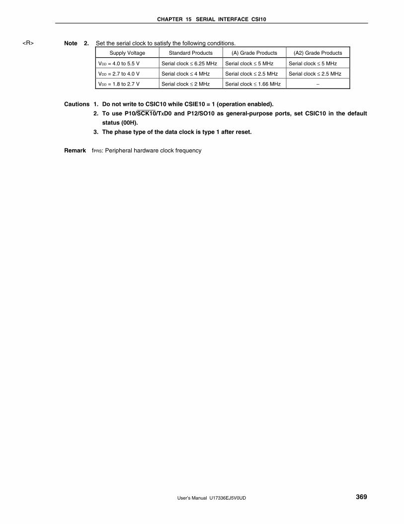
CHAPTER 15 SERIAL INTERFACE CSI10
User’s Manual U17336EJ5V0UD 369
Note 2. Set the serial clock to satisfy the following conditions.
Supply Voltage Standard Products (A) Grade Products (A2) Grade Products
VDD = 4.0 to 5.5 V Serial clock ≤ 6.25 MHz Serial clock ≤ 5 MHz Serial clock ≤ 5 MHz
VDD = 2.7 to 4.0 V Serial clock ≤ 4 MHz Serial clock ≤ 2.5 MHz Serial clock ≤ 2.5 MHz
VDD = 1.8 to 2.7 V Serial clock ≤ 2 MHz Serial clock ≤ 1.66 MHz −
Cautions 1. Do not write to CSIC10 while CSIE10 = 1 (operation enabled).
2. To use P10/SCK10/TXD0 and P12/SO10 as general-purpose ports, set CSIC10 in the default
status (00H).
3. The phase type of the data clock is type 1 after reset.
Remark fPRS: Peripheral hardware clock frequency
<R>

CHAPTER 15 SERIAL INTERFACE CSI10
User’s Manual U17336EJ5V0UD 370
(3) Port mode register 1 (PM1)
This register sets port 1 input/output in 1-bit units.
When using P10/SCK10 as the clock output pin of the serial interface, clear PM10 to 0, and set the output latch of
P10 to 1.
When using P12/SO10 as the data output pin of the serial interface, clear PM12 and the output latch of P12 to 0.
When using P10/SCK10/TxD0 as the clock input pin of the serial interface, P11/SI10/RXD0 as the data input pin,
set PM10 and PM11 to 1. At this time, the output latches of P10 and P11 may be 0 or 1.
PM1 can be set by a 1-bit or 8-bit memory manipulation instruction.
Reset signal generation sets this register to FFH.
Figure 15-4. Format of Port Mode Register 1 (PM1)
7
PM17
6
PM16
5
PM15
4
PM14
3
PM13
2
PM12
1
PM11
0
PM10
Symbol
PM1
Address: FF21H After reset: FFH R/W
PM1n
0
1
P1n pin I/O mode selection (n = 0 to 7)
Output mode (output buffer on)
Input mode (output buffer off)

CHAPTER 15 SERIAL INTERFACE CSI10
User’s Manual U17336EJ5V0UD 371
15.4 Operation of Serial Interface CSI10
Serial interface CSI10 can be used in the following two modes.
• Operation stop mode
• 3-wire serial I/O mode
15.4.1 Operation stop mode
Serial communication is not executed in this mode. Therefore, the power consumption can be reduced. In
addition, the P10/SCK10/TXD0, P11/SI10/RXD0, and P12/SO10 pins can be used as ordinary I/O port pins in this
mode.
(1) Register used
The operation stop mode is set by serial operation mode register 10 (CSIM10).
To set the operation stop mode, clear bit 7 (CSIE10) of CSIM10 to 0.
(a) Serial operation mode register 10 (CSIM10)
CSIM10 can be set by a 1-bit or 8-bit memory manipulation instruction.
Reset signal generation sets CSIM10 to 00H.
Address: FF80H After reset: 00H R/W
Symbol <7> 6 5 4 3 2 1 0
CSIM10 CSIE10 TRMD10 0 DIR10 0 0 0 CSOT10
CSIE10 Operation control in 3-wire serial I/O mode
0 Disables operationNote 1 and asynchronously resets the internal circuitNote 2.
Notes 1. To use P10/SCK10/TXD0 and P12/SO10 as general-purpose ports, set CSIM10 in the default
status (00H).
2. Bit 0 (CSOT10) of CSIM10 and serial I/O shift register 10 (SIO10) are reset.
15.4.2 3-wire serial I/O mode
The 3-wire serial I/O mode is used for connecting peripheral ICs and display controllers with a clocked serial
interface.
In this mode, communication is executed by using three lines: the serial clock (SCK10), serial output (SO10), and
serial input (SI10) lines.
(1) Registers used
• Serial operation mode register 10 (CSIM10)
• Serial clock selection register 10 (CSIC10)
• Port mode register 1 (PM1)
• Port register 1 (P1)

CHAPTER 15 SERIAL INTERFACE CSI10
User’s Manual U17336EJ5V0UD 372
The basic procedure of setting an operation in the 3-wire serial I/O mode is as follows.
<1> Set the CSIC10 register (see Figure 15-3).
<2> Set bits 4, and 6 (DIR10, and TRMD10) of the CSIM10 register (see Figure 15-2).
<3> Set bit 7 (CSIE10) of the CSIM10 register to 1. → Transmission/reception is enabled.
<4> Write data to transmit buffer register 10 (SOTB10). → Data transmission/reception is started.
Read data from serial I/O shift register 10 (SIO10). → Data reception is started.
Caution Take the relationship with the other party of communication when setting the port mode
register and port register.
The relationship between the register settings and pins is shown below.
Table 15-2. Relationship Between Register Settings and Pins
Pin Function CSIE10 TRMD10 PM11 P11 PM12 P12 PM10 P10 CSI10
Operation SI10/RXD0/
P11
SO10/P12 SCK10/
TXD0/P10
0 × ×Note 1 ×Note 1 ×Note 1 ×Note 1 ×Note 1 ×Note 1 Stop RXD0/P11 P12 TXD0/
P10Note 2
1 0 1 × ×Note 1 ×Note 1 1 × Slave
receptionNote 3
SI10 P12 SCK10
(input)Note 3
1 1 ×Note 1 ×Note 1 0 0 1 × Slave
transmissionNote 3
RXD0/P11 SO10 SCK10
(input)Note 3
1 1 1 × 0 0 1 × Slave
transmission/
receptionNote 3
SI10 SO10 SCK10
(input)Note 3
1 0 1 × ×Note 1 ×Note 1 0 1 Master reception SI10 P12 SCK10
(output)
1 1 ×Note 1 ×Note 1 0 0 0 1 Master
transmission
RXD0/P11 SO10 SCK10
(output)
1 1 1 × 0 0 0 1 Master
transmission/
reception
SI10 SO10 SCK10
(output)
Notes 1. Can be set as port function.
2. To use P10/SCK10/TXD0 as port pins, clear CKP10 to 0.
3. To use the slave mode, set CKS102, CKS101, and CKS100 to 1, 1, 1.
Remark ×: don’t care
CSIE10: Bit 7 of serial operation mode register 10 (CSIM10)
TRMD10: Bit 6 of CSIM10
CKP10: Bit 4 of serial clock selection register 10 (CSIC10)
CKS102, CKS101, CKS100: Bits 2 to 0 of CSIC10
PM1×: Port mode register
P1×: Port output latch
CHAPTER 15 SERIAL INTERFACE CSI10
User’s Manual U17336EJ5V0UD 373
(2) Communication operation
In the 3-wire serial I/O mode, data is transmitted or received in 8-bit units. Each bit of the data is transmitted or
received in synchronization with the serial clock.
Data can be transmitted or received if bit 6 (TRMD10) of serial operation mode register 10 (CSIM10) is 1.
Transmission/reception is started when a value is written to transmit buffer register 10 (SOTB10). In addition,
data can be received when bit 6 (TRMD10) of serial operation mode register 10 (CSIM10) is 0.
Reception is started when data is read from serial I/O shift register 10 (SIO10).
After communication has been started, bit 0 (CSOT10) of CSIM10 is set to 1. When communication of 8-bit data
has been completed, a communication completion interrupt request flag (CSIIF10) is set, and CSOT10 is cleared
to 0. Then the next communication is enabled.
Caution Do not access the control register and data register when CSOT10 = 1 (during serial
communication).
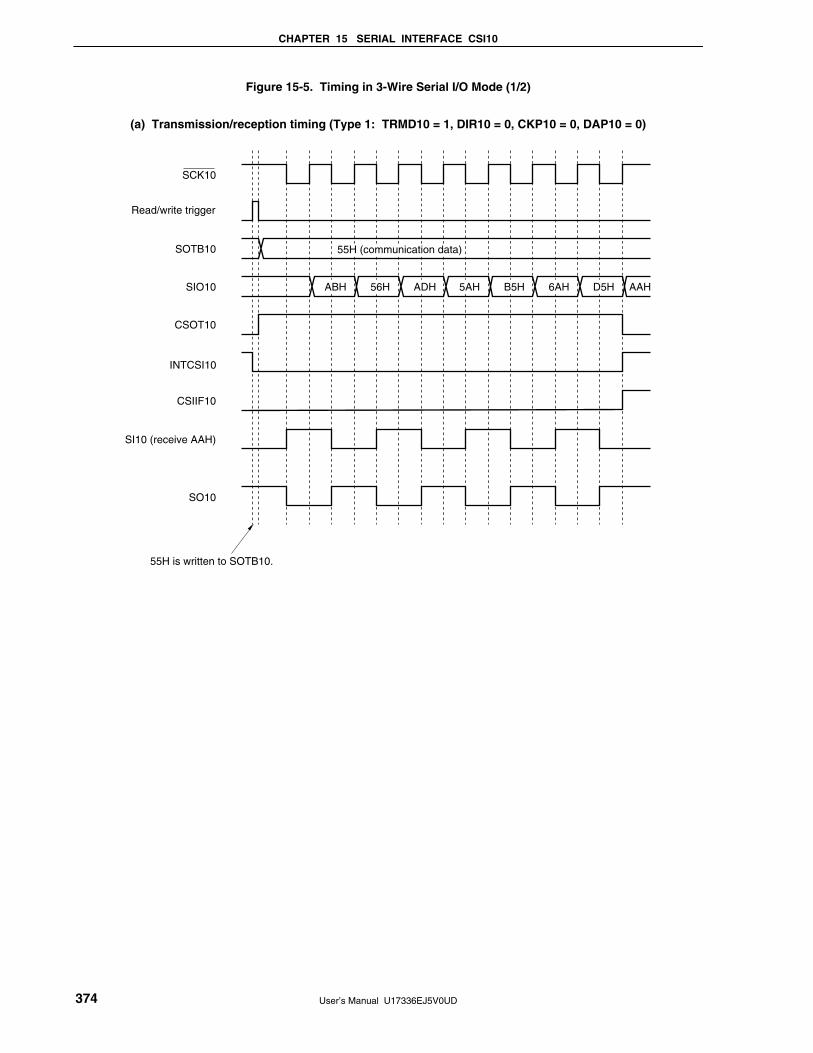
CHAPTER 15 SERIAL INTERFACE CSI10
User’s Manual U17336EJ5V0UD 374
Figure 15-5. Timing in 3-Wire Serial I/O Mode (1/2)
(a) Transmission/reception timing (Type 1: TRMD10 = 1, DIR10 = 0, CKP10 = 0, DAP10 = 0)
AAHABH 56H ADH 5AH B5H 6AH D5H
55H (communication data)
55H is written to SOTB10.
SCK10
SOTB10
SIO10
CSOT10
CSIIF10
SO10
SI10 (receive AAH)
Read/write trigger
INTCSI10

CHAPTER 15 SERIAL INTERFACE CSI10
User’s Manual U17336EJ5V0UD 375
Figure 15-5. Timing in 3-Wire Serial I/O Mode (2/2)
(b) Transmission/reception timing (Type 2: TRMD10 = 1, DIR10 = 0, CKP10 = 0, DAP10 = 1)
ABH 56H ADH 5AH B5H 6AH D5H
SCK10
SOTB10
SIO10
CSOT10
CSIIF10
SO10
SI10 (input AAH)
AAH
55H (communication data)
55H is written to SOTB10.
Read/write trigger
INTCSI10

CHAPTER 15 SERIAL INTERFACE CSI10
User’s Manual U17336EJ5V0UD 376
Figure 15-6. Timing of Clock/Data Phase
(a) Type 1: CKP10 = 0, DAP10 = 0, DIR10 = 0
D7 D6 D5 D4 D3 D2 D1 D0
SCK10
SO10 Writing to SOTB10 or
reading from SIO10
SI10 capture
CSIIF10
CSOT10
(b) Type 2: CKP10 = 0, DAP10 = 1, DIR10 = 0
D7 D6 D5 D4 D3 D2 D1 D0
SCK10
SO10Writing to SOTB10 or
reading from SIO10
SI10 capture
CSIIF10
CSOT10
(c) Type 3: CKP10 = 1, DAP10 = 0, DIR10 = 0
D7 D6 D5 D4 D3 D2 D1 D0
SCK10
SO10Writing to SOTB10 or
reading from SIO10
SI10 capture
CSIIF10
CSOT10
(d) Type 4: CKP10 = 1, DAP10 = 1, DIR10 = 0
D7 D6 D5 D4 D3 D2 D1 D0
SCK10
SO10Writing to SOTB10 or
reading from SIO10
SI10 capture
CSIIF10
CSOT10
Remark The above figure illustrates a communication operation where data is transmitted with the MSB first.

CHAPTER 15 SERIAL INTERFACE CSI10
User’s Manual U17336EJ5V0UD 377
(3) Timing of output to SO10 pin (first bit)
When communication is started, the value of transmit buffer register 10 (SOTB10) is output from the SO10 pin.
The output operation of the first bit at this time is described below.
Figure 15-7. Output Operation of First Bit (1/2)
(a) Type 1: CKP10 = 0, DAP10 = 0
SCK10
SOTB10
SIO10
SO10
Writing to SOTB10 orreading from SIO10
First bit 2nd bit
Output latch
(b) Type 3: CKP10 = 1, DAP10 = 0
SCK10
SOTB10
SIO10
Output latch
SO10
Writing to SOTB10 orreading from SIO10
First bit 2nd bit
The first bit is directly latched by the SOTB10 register to the output latch at the falling (or rising) edge of SCK10,
and output from the SO10 pin via an output selector. Then, the value of the SOTB10 register is transferred to the
SIO10 register at the next rising (or falling) edge of SCK10, and shifted one bit. At the same time, the first bit of
the receive data is stored in the SIO10 register via the SI10 pin.
The second and subsequent bits are latched by the SIO10 register to the output latch at the next falling (or rising)
edge of SCK10, and the data is output from the SO10 pin.

CHAPTER 15 SERIAL INTERFACE CSI10
User’s Manual U17336EJ5V0UD 378
Figure 15-7. Output Operation of First Bit (2/2)
(c) Type 2: CKP10 = 0, DAP10 = 1
SCK10
SOTB10
SIO10
SO10
Writing to SOTB10 orreading from SIO10
First bit 2nd bit 3rd bit
Output latch
(d) Type 4: CKP10 = 1, DAP10 = 1
First bit 2nd bit 3rd bit
SCK10
SOTB10
SIO10
Output latch
SO10
Writing to SOTB10 orreading from SIO10
The first bit is directly latched by the SOTB10 register at the falling edge of the write signal of the SOTB10
register or the read signal of the SIO10 register, and output from the SO10 pin via an output selector. Then, the
value of the SOTB10 register is transferred to the SIO10 register at the next falling (or rising) edge of SCK10, and
shifted one bit. At the same time, the first bit of the receive data is stored in the SIO10 register via the SI10 pin.
The second and subsequent bits are latched by the SIO10 register to the output latch at the next rising (or falling)
edge of SCK10, and the data is output from the SO10 pin.

CHAPTER 15 SERIAL INTERFACE CSI10
User’s Manual U17336EJ5V0UD 379
(4) Output value of SO10 pin (last bit)
After communication has been completed, the SO10 pin holds the output value of the last bit.
Figure 15-8. Output Value of SO10 Pin (Last Bit) (1/2)
(a) Type 1: CKP10 = 0, DAP10 = 0
SCK10
SOTB10
SIO10
SO10
Writing to SOTB10 orreading from SIO10
( ← Next request is issued.)
Last bit
Output latch
(b) Type 3: CKP10 = 1, DAP10 = 0
Last bit
( ← Next request is issued.)
SCK10
SOTB10
SIO10
Output latch
SO10
Writing to SOTB10 orreading from SIO10

CHAPTER 15 SERIAL INTERFACE CSI10
User’s Manual U17336EJ5V0UD 380
Figure 15-8. Output Value of SO10 Pin (Last Bit) (2/2)
(c) Type 2: CKP10 = 0, DAP10 = 1
SCK10
SOTB10
SIO10
SO10 Last bit
Writing to SOTB10 orreading from SIO10
( ← Next request is issued.)
Output latch
(d) Type 4: CKP10 = 1, DAP10 = 1
Last bit
( ← Next request is issued.)
SCK10
SOTB10
SIO10
Output latch
SO10
Writing to SOTB10 orreading from SIO10

CHAPTER 15 SERIAL INTERFACE CSI10
User’s Manual U17336EJ5V0UD 381
(5) SO10 output (see Figure 15-1)
The status of the SO10 output is as follows if bit 7 (CSIE10) of serial operation mode register 10 (CSIM10) is
cleared to 0.
Table 15-3. SO10 Output Status
TRMD10 DAP10 DIR10 SO10 OutputNote 1
TRMD10 = 0Note 2 − − Outputs low levelNote 2
DAP10 = 0 − Value of SO10 latch
(low-level output)
DIR10 = 0 Value of bit 7 of SOTB10
TRMD10 = 1
DAP10 = 1
DIR10 = 1 Value of bit 0 of SOTB10
Notes 1. The actual output of the SO10/P12 pin is determined according to PM12 and P12, as well as
the SO10 output.
2. Status after reset
Caution If a value is written to TRMD10, DAP10, and DIR10, the output value of SO10 changes.

User’s Manual U17336EJ5V0UD 382
CHAPTER 16 SERIAL INTERFACE IIC0
16.1 Functions of Serial Interface IIC0
Serial interface IIC0 has the following two modes.
(1) Operation stop mode
This mode is used when serial transfers are not performed. It can therefore be used to reduce power
consumption.
(2) I2C bus mode (multimaster supported)
This mode is used for 8-bit data transfers with several devices via two lines: a serial clock (SCL0) line and a
serial data bus (SDA0) line.
This mode complies with the I2C bus format and the master device can generated “start condition”, “address”,
“transfer direction specification”, “data”, and “stop condition” data to the slave device, via the serial data bus.
The slave device automatically detects these received status and data by hardware. This function can simplify
the part of application program that controls the I2C bus.
Since the SCL0 and SDA0 pins are used for open drain outputs, IIC0 requires pull-up resistors for the serial
clock line and the serial data bus line.
Caution Do not use serial interface IIC0 and the multiplier/divider simultaneously, because various
flags corresponding to interrupt request sources are shared among serial interface IIC0 and
the multiplier/divider.
Figure 16-1 shows a block diagram of serial interface IIC0.
<R>
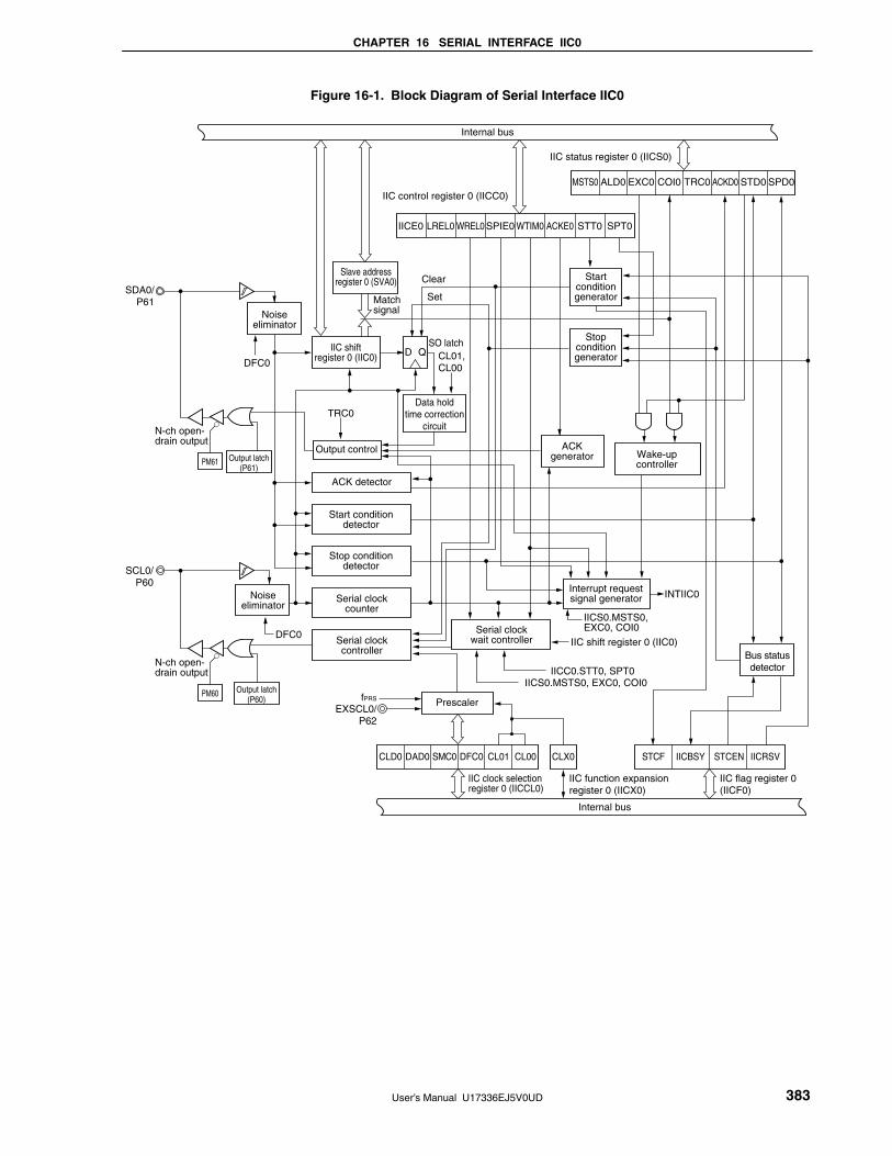
CHAPTER 16 SERIAL INTERFACE IIC0
User’s Manual U17336EJ5V0UD 383
Figure 16-1. Block Diagram of Serial Interface IIC0
Internal bus
IIC status register 0 (IICS0)
IIC control register 0 (IICC0)
Slave addressregister 0 (SVA0)
Noiseeliminator
Noiseeliminator
Bus statusdetector
Match signal
IIC shiftregister 0 (IIC0)
SO latch
IICE0
D Q
Set
Clear
CL01,CL00
TRC0
DFC0
DFC0
SDA0/P61
SCL0/P60
Data holdtime correction
circuit
Startconditiongenerator
Stopconditiongenerator
ACKgenerator Wake-up
controller
ACK detector
Output control
Stop conditiondetector
Serial clockcounter
Interrupt requestsignal generator
Serial clockcontroller
Serial clockwait controller
Prescaler
INTIIC0
IIC shift register 0 (IIC0)
IICC0.STT0, SPT0IICS0.MSTS0, EXC0, COI0
IICS0.MSTS0, EXC0, COI0
fPRS
LREL0 WREL0 SPIE0 WTIM0 ACKE0 STT0 SPT0
MSTS0 ALD0 EXC0 COI0 TRC0 ACKD0 STD0 SPD0
Start conditiondetector
Internal bus
CLD0 DAD0 SMC0 DFC0 CL01 CL00 CLX0
IIC clock selectionregister 0 (IICCL0)
STCF IICBSY STCEN IICRSV
IIC flag register 0(IICF0)
IIC function expansion register 0 (IICX0)
N-ch open-drain output
PM61 Output latch(P61)
N-ch open-drain output
PM60 Output latch(P60)
EXSCL0/P62

CHAPTER 16 SERIAL INTERFACE IIC0
User’s Manual U17336EJ5V0UD 384
Figure 16-2 shows a serial bus configuration example.
Figure 16-2. Serial Bus Configuration Example Using I2C Bus
Master CPU1
Slave CPU1
Address 0
SDA0
SCL0
Serial data bus
Serial clock
+ VDD + VDD
SDA0
SCL0
SDA0
SCL0
SDA0
SCL0
SDA0
SCL0
Master CPU2
Slave CPU2
Address 1
Slave CPU3
Address 2
Slave IC
Address 3
Slave IC
Address N

CHAPTER 16 SERIAL INTERFACE IIC0
User’s Manual U17336EJ5V0UD 385
16.2 Configuration of Serial Interface IIC0
Serial interface IIC0 includes the following hardware.
Table 16-1. Configuration of Serial Interface IIC0
Item Configuration
Registers IIC shift register 0 (IIC0) Slave address register 0 (SVA0)
Control registers IIC control register 0 (IICC0) IIC status register 0 (IICS0) IIC flag register 0 (IICF0) IIC clock selection register 0 (IICCL0) IIC function expansion register 0 (IICX0) Port mode register 6 (PM6) Port register 6 (P6)
(1) IIC shift register 0 (IIC0)
IIC0 is used to convert 8-bit serial data to 8-bit parallel data and vice versa in synchronization with the serial
clock. IIC0 can be used for both transmission and reception.
The actual transmit and receive operations can be controlled by writing and reading operations to IIC0.
Cancel the wait state and start data transfer by writing data to IIC0 during the wait period.
IIC0 is set by an 8-bit memory manipulation instruction.
Reset signal generation clears IIC0 to 00H.
Figure 16-3. Format of IIC Shift Register 0 (IIC0)
Symbol
IIC0
Address: FFA5H After reset: 00H R/W
7 6 5 4 3 2 1 0
Cautions 1. Do not write data to IIC0 during data transfer.
2. Write or read IIC0 only during the wait period. Accessing IIC0 in a communication state
other than during the wait period is prohibited. When the device serves as the master,
however, IIC0 can be written only once after the communication trigger bit (STT0) is set to
1.
(2) Slave address register 0 (SVA0)
This register stores local addresses when in slave mode.
SVA0 is set by an 8-bit memory manipulation instruction.
However, rewriting to this register is prohibited while STD0 = 1 (while the start condition is detected).
Reset signal generation clears SVA0 to 00H.
Figure 16-4. Format of Slave Address Register 0 (SVA0)
Symbol
SVA0
Address: FFA7H After reset: 00H R/W
7 6 5 4 3 2 1 0
0Note
Note Bit 0 is fixed to 0.

CHAPTER 16 SERIAL INTERFACE IIC0
User’s Manual U17336EJ5V0UD 386
(3) SO latch
The SO latch is used to retain the SDA0 pin’s output level.
(4) Wake-up controller
This circuit generates an interrupt request (INTIIC0) when the address received by this register matches the
address value set to slave address register 0 (SVA0) or when an extension code is received.
(5) Prescaler
This selects the sampling clock to be used.
(6) Serial clock counter
This counter counts the serial clocks that are output or input during transmit/receive operations and is used to
verify that 8-bit data was transmitted or received.
(7) Interrupt request signal generator
This circuit controls the generation of interrupt request signals (INTIIC0).
An I2C interrupt request is generated by the following two triggers.
• Falling edge of eighth or ninth clock of the serial clock (set by WTIM0 bit)
• Interrupt request generated when a stop condition is detected (set by SPIE0 bit)
Remark WTIM0 bit: Bit 3 of IIC control register 0 (IICC0)
SPIE0 bit: Bit 4 of IIC control register 0 (IICC0)
(8) Serial clock controller
In master mode, this circuit generates the clock output via the SCL0 pin from a sampling clock.
(9) Serial clock wait controller
This circuit controls the wait timing.
(10) ACK generator, stop condition detector, start condition detector, and ACK detector
These circuits generate and detect each status.
(11) Data hold time correction circuit
This circuit generates the hold time for data corresponding to the falling edge of the serial clock.
(12) Start condition generator
This circuit generates a start condition when the STT0 bit is set to 1.
However, in the communication reservation disabled status (IICRSV bit = 1), when the bus is not released
(IICBSY bit = 1), start condition requests are ignored and the STCF bit is set to 1.
(13) Stop condition generator
This circuit generates a stop condition when the SPT0 bit is set to 1.

CHAPTER 16 SERIAL INTERFACE IIC0
User’s Manual U17336EJ5V0UD 387
(14) Bus status detector
This circuit detects whether or not the bus is released by detecting start conditions and stop conditions.
However, as the bus status cannot be detected immediately following operation, the initial status is set by the
STCEN bit.
Remark STT0 bit: Bit 1 of IIC control register 0 (IICC0)
SPT0 bit: Bit 0 of IIC control register 0 (IICC0)
IICRSV bit: Bit 0 of IIC flag register 0 (IICF0)
IICBSY bit: Bit 6 of IIC flag register 0 (IICF0)
STCF bit: Bit 7 of IIC flag register 0 (IICF0)
STCEN bit: Bit 1 of IIC flag register 0 (IICF0)

CHAPTER 16 SERIAL INTERFACE IIC0
User’s Manual U17336EJ5V0UD 388
16.3 Registers to Control Serial Interface IIC0
Serial interface IIC0 is controlled by the following seven registers.
• IIC control register 0 (IICC0)
• IIC flag register 0 (IICF0)
• IIC status register 0 (IICS0)
• IIC clock selection register 0 (IICCL0)
• IIC function expansion register 0 (IICX0)
• Port mode register 6 (PM6)
• Port register 6 (P6)
(1) IIC control register 0 (IICC0)
This register is used to enable/stop I2C operations, set wait timing, and set other I2C operations.
IICC0 is set by a 1-bit or 8-bit memory manipulation instruction. However, set the SPIE0, WTIM0, and ACKE0
bits while IICE0 bit = 0 or during the wait period. These bits can be set at the same time when the IICE0 bit is
set from “0” to “1”.
Reset signal generation clears IICC0 to 00H.

CHAPTER 16 SERIAL INTERFACE IIC0
User’s Manual U17336EJ5V0UD 389
Figure 16-5. Format of IIC Control Register 0 (IICC0) (1/4)
Address: FFA6H After reset: 00H R/W
Symbol <7> <6> <5> <4> <3> <2> <1> <0>
IICC0 IICE0 LREL0 WREL0 SPIE0 WTIM0 ACKE0 STT0 SPT0
IICE0 I2C operation enable
0 Stop operation. Reset IIC status register 0 (IICS0)Note 1. Stop internal operation.
1 Enable operation.
Be sure to set this bit (1) while the SCL0 and SDA0 lines are at high level.
Condition for clearing (IICE0 = 0) Condition for setting (IICE0 = 1)
• Cleared by instruction
• Reset
• Set by instruction
LREL0Note 2 Exit from communications
0 Normal operation
1 This exits from the current communications and sets standby mode. This setting is automatically cleared to 0
after being executed.
Its uses include cases in which a locally irrelevant extension code has been received.
The SCL0 and SDA0 lines are set to high impedance.
The following flags of IIC control register 0 (IICC0) and IIC status register 0 (IICS0) are cleared to 0. • STT0 • SPT0 • MSTS0 • EXC0 • COI0 • TRC0 • ACKD0 • STD0
The standby mode following exit from communications remains in effect until the following communications entry conditions
are met.
• After a stop condition is detected, restart is in master mode.
• An address match or extension code reception occurs after the start condition.
Condition for clearing (LREL0 = 0) Condition for setting (LREL0 = 1)
• Automatically cleared after execution
• Reset
• Set by instruction
WREL0Note 2 Wait cancellation
0 Do not cancel wait
1 Cancel wait. This setting is automatically cleared after wait is canceled.
When WREL0 is set (wait canceled) during the wait period at the ninth clock pulse in the transmission status (TRC0 = 1), the
SDA0 line goes into the high impedance state (TRC0 = 0).
Condition for clearing (WREL0 = 0) Condition for setting (WREL0 = 1)
• Automatically cleared after execution
• Reset
• Set by instruction
Notes 1. The IICS0 register, the STCF0 and IICBSY bits of the IICF0 register, and the CLD0 and DAD0 bits of the
IICCL0 register are reset.
2. This flag’s signal is invalid when IICE0 = 0.
Caution The start condition is detected immediately after I2C is enabled to operate (IICE0 = 1) while the
SCL0 line is at high level and the SDA0 line is at low level. Immediately after enabling I2C to
operate (IICE0 = 1), set LREL0 (1) by using a 1-bit memory manipulation instruction.

CHAPTER 16 SERIAL INTERFACE IIC0
User’s Manual U17336EJ5V0UD 390
Figure 16-5. Format of IIC Control Register 0 (IICC0) (2/4)
SPIE0Note 1 Enable/disable generation of interrupt request when stop condition is detected
0 Disable
1 Enable
Condition for clearing (SPIE0 = 0) Condition for setting (SPIE0 = 1)
• Cleared by instruction
• Reset
• Set by instruction
WTIM0Note 1 Control of wait and interrupt request generation
0 Interrupt request is generated at the eighth clock’s falling edge.
Master mode: After output of eight clocks, clock output is set to low level and wait is set.
Slave mode: After input of eight clocks, the clock is set to low level and wait is set for master device.
1 Interrupt request is generated at the ninth clock’s falling edge.
Master mode: After output of nine clocks, clock output is set to low level and wait is set.
Slave mode: After input of nine clocks, the clock is set to low level and wait is set for master device.
An interrupt is generated at the falling edge of the ninth clock during address transfer independently of the setting of this bit.
The setting of this bit is valid when the address transfer is completed. When in master mode, a wait is inserted at the falling
edge of the ninth clock during address transfers. For a slave device that has received a local address, a wait is inserted at the
falling edge of the ninth clock after an acknowledge (ACK) is issued. However, when the slave device has received an
extension code, a wait is inserted at the falling edge of the eighth clock.
Condition for clearing (WTIM0 = 0) Condition for setting (WTIM0 = 1)
• Cleared by instruction
• Reset
• Set by instruction
ACKE0Notes 1, 2 Acknowledgment control
0 Disable acknowledgment.
1 Enable acknowledgment. During the ninth clock period, the SDA0 line is set to low level.
Condition for clearing (ACKE0 = 0) Condition for setting (ACKE0 = 1)
• Cleared by instruction
• Reset
• Set by instruction
Notes 1. This flag’s signal is invalid when IICE0 = 0.
2. The set value is invalid during address transfer and if the code is not an extension code.
When the device serves as a slave and the addresses match, an acknowledge is generated regardless
of the set value.


CHAPTER 16 SERIAL INTERFACE IIC0
User’s Manual U17336EJ5V0UD 392
Figure 16-5. Format of IIC Control Register 0 (IICC0) (4/4)
SPT0 Stop condition trigger
0 Stop condition is not generated.
1 Stop condition is generated (termination of master device’s transfer).
After the SDA0 line goes to low level, either set the SCL0 line to high level or wait until it goes to high level. Next,
after the rated amount of time has elapsed, the SDA0 line changes from low level to high level and a stop
condition is generated.
Cautions concerning set timing
• For master reception: Cannot be set to 1 during transfer.
Can be set to 1 only in the waiting period when ACKE0 has been cleared to 0 and slave has been
notified of final reception.
• For master transmission: A stop condition cannot be generated normally during the acknowledge period. Therefore, set it
during the wait period that follows output of the ninth clock.
• Cannot be set to 1 at the same time as STT0.
• SPT0 can be set to 1 only when in master modeNote.
• When WTIM0 has been cleared to 0, if SPT0 is set to 1 during the wait period that follows output of eight clocks, note that a
stop condition will be generated during the high-level period of the ninth clock. WTIM0 should be changed from 0 to 1 during
the wait period following the output of eight clocks, and SPT0 should be set to 1 during the wait period that follows the output
of the ninth clock.
• Setting SPT0 to 1 and then setting it again before it is cleared to 0 is prohibited.
Condition for clearing (SPT0 = 0) Condition for setting (SPT0 = 1)
• Cleared by loss in arbitration
• Automatically cleared after stop condition is detected
• Cleared by LREL0 = 1 (exit from communications)
• When IICE0 = 0 (operation stop)
• Reset
• Set by instruction
Note Set SPT0 to 1 only in master mode. However, SPT0 must be set to 1 and a stop condition generated before
the first stop condition is detected following the switch to the operation enabled status. For details, see
16.5.15 Cautions.
Caution When bit 3 (TRC0) of IIC status register 0 (IICS0) is set to 1, WREL0 is set to 1 during the ninth
clock and wait is canceled, after which TRC0 is cleared and the SDA0 line is set to high
impedance.
Remark Bit 0 (SPT0) becomes 0 when it is read after data setting.

CHAPTER 16 SERIAL INTERFACE IIC0
User’s Manual U17336EJ5V0UD 393
(2) IIC status register 0 (IICS0)
This register indicates the status of I2C.
IICS0 is read by a 1-bit or 8-bit memory manipulation instruction only when STT0 = 1 and during the wait
period.
Reset signal generation clears IICS0 to 00H.
Caution If data is read from IICS0, a wait cycle is generated. Do not read data from IICS0 when the
CPU is operating on the subsystem clock and the peripheral hardware clock is stopped. For
details, see CHAPTER 34 CAUTIONS FOR WAIT.
Figure 16-6. Format of IIC Status Register 0 (IICS0) (1/3)
Address: FFAAH After reset: 00H R
Symbol <7> <6> <5> <4> <3> <2> <1> <0>
IICS0 MSTS0 ALD0 EXC0 COI0 TRC0 ACKD0 STD0 SPD0
MSTS0 Master device status
0 Slave device status or communication standby status
1 Master device communication status
Condition for clearing (MSTS0 = 0) Condition for setting (MSTS0 = 1)
• When a stop condition is detected • When ALD0 = 1 (arbitration loss) • Cleared by LREL0 = 1 (exit from communications) • When IICE0 changes from 1 to 0 (operation stop) • Reset
• When a start condition is generated
ALD0 Detection of arbitration loss
0 This status means either that there was no arbitration or that the arbitration result was a “win”.
1 This status indicates the arbitration result was a “loss”. MSTS0 is cleared.
Condition for clearing (ALD0 = 0) Condition for setting (ALD0 = 1)
• Automatically cleared after IICS0 is readNote
• When IICE0 changes from 1 to 0 (operation stop) • Reset
• When the arbitration result is a “loss”.
EXC0 Detection of extension code reception
0 Extension code was not received.
1 Extension code was received.
Condition for clearing (EXC0 = 0) Condition for setting (EXC0 = 1)
• When a start condition is detected • When a stop condition is detected • Cleared by LREL0 = 1 (exit from communications) • When IICE0 changes from 1 to 0 (operation stop) • Reset
• When the higher four bits of the received address data is either “0000” or “1111” (set at the rising edge of the eighth clock).
Note This register is also cleared when a 1-bit memory manipulation instruction is executed for bits other
than IICS0. Therefore, when using the ALD0 bit, read the data of this bit before the data of the other
bits.
Remark LREL0: Bit 6 of IIC control register 0 (IICC0)
IICE0: Bit 7 of IIC control register 0 (IICC0)

CHAPTER 16 SERIAL INTERFACE IIC0
User’s Manual U17336EJ5V0UD 394
Figure 16-6. Format of IIC Status Register 0 (IICS0) (2/3)
COI0 Detection of matching addresses
0 Addresses do not match.
1 Addresses match.
Condition for clearing (COI0 = 0) Condition for setting (COI0 = 1)
• When a start condition is detected
• When a stop condition is detected
• Cleared by LREL0 = 1 (exit from communications)
• When IICE0 changes from 1 to 0 (operation stop)
• Reset
• When the received address matches the local address
(slave address register 0 (SVA0))
(set at the rising edge of the eighth clock).
TRC0 Detection of transmit/receive status
0 Receive status (other than transmit status). The SDA0 line is set for high impedance.
1 Transmit status. The value in the SO0 latch is enabled for output to the SDA0 line (valid starting at the
falling edge of the first byte’s ninth clock).
Condition for clearing (TRC0 = 0) Condition for setting (TRC0 = 1)
<Both master and slave>
• When a stop condition is detected
• Cleared by LREL0 = 1 (exit from communications)
• When IICE0 changes from 1 to 0 (operation stop)
• Cleared by WREL0 = 1Note (wait cancel)
• When ALD0 changes from 0 to 1 (arbitration loss)
• Reset
<Master>
• When “1” is output to the first byte’s LSB (transfer
direction specification bit)
<Slave>
• When a start condition is detected
• When “0” is input to the first byte’s LSB (transfer direction
specification bit)
<When not used for communication>
<Master>
• When a start condition is generated
• When “0” is output to the first byte’s LSB (transfer
direction specification bit)
<Slave>
• When “1” is input to the first byte’s LSB (transfer
direction specification bit)
Note If the wait state is canceled by setting bit 5 (WREL0) of IIC control register 0 (IICC0) to 1 at the ninth
clock when bit 3 (TRC0) of IIC status register 0 (IICS0) is 1, TRC0 is cleared, and the SDA0 line goes
into a high-impedance state.
Remark LREL0: Bit 6 of IIC control register 0 (IICC0)
IICE0: Bit 7 of IIC control register 0 (IICC0)

CHAPTER 16 SERIAL INTERFACE IIC0
User’s Manual U17336EJ5V0UD 395
Figure 16-6. Format of IIC Status Register 0 (IICS0) (3/3)
ACKD0 Detection of ACK
0 ACK was not detected.
1 ACK was detected.
Condition for clearing (ACKD0 = 0) Condition for setting (ACKD0 = 1)
• When a stop condition is detected
• At the rising edge of the next byte’s first clock
• Cleared by LREL0 = 1 (exit from communications)
• When IICE0 changes from 1 to 0 (operation stop)
• Reset
• After the SDA0 line is set to low level at the rising edge of
SCL0’s ninth clock
STD0 Detection of start condition
0 Start condition was not detected.
1 Start condition was detected. This indicates that the address transfer period is in effect.
Condition for clearing (STD0 = 0) Condition for setting (STD0 = 1)
• When a stop condition is detected
• At the rising edge of the next byte’s first clock following
address transfer
• Cleared by LREL0 = 1 (exit from communications)
• When IICE0 changes from 1 to 0 (operation stop)
• Reset
• When a start condition is detected
SPD0 Detection of stop condition
0 Stop condition was not detected.
1 Stop condition was detected. The master device’s communication is terminated and the bus is released.
Condition for clearing (SPD0 = 0) Condition for setting (SPD0 = 1)
• At the rising edge of the address transfer byte’s first
clock following setting of this bit and detection of a start
condition
• When IICE0 changes from 1 to 0 (operation stop)
• Reset
• When a stop condition is detected
Remark LREL0: Bit 6 of IIC control register 0 (IICC0)
IICE0: Bit 7 of IIC control register 0 (IICC0)
(3) IIC flag register 0 (IICF0)
This register sets the operation mode of I2C and indicates the status of the I2C bus.
IICF0 is set by a 1-bit or 8-bit memory manipulation instruction. However, the STCF and IICBSY bits are read-
only.
The IICRSV bit can be used to enable/disable the communication reservation function (see 16.5.14
Communication reservation).
STCEN can be used to set the initial value of the IICBSY bit (see 16.5.15 Cautions).
IICRSV and STCEN can be written only when the operation of I2C is disabled (bit 7 (IICE0) of IIC control
register 0 (IICC0) = 0). When operation is enabled, the IICF0 register can be read.
Reset signal generation clears IICF0 to 00H.
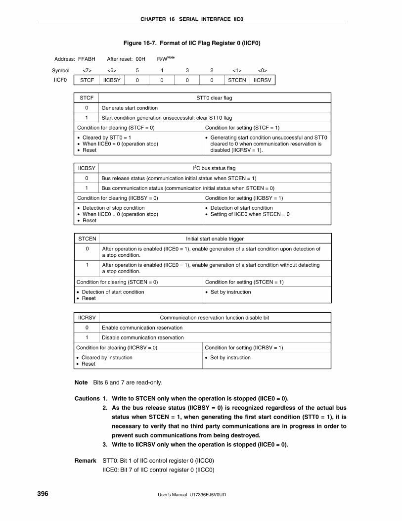
CHAPTER 16 SERIAL INTERFACE IIC0
User’s Manual U17336EJ5V0UD 396
Figure 16-7. Format of IIC Flag Register 0 (IICF0)
<7>
STCF
Condition for clearing (STCF = 0)
• Cleared by STT0 = 1 • When IICE0 = 0 (operation stop)• Reset
Condition for setting (STCF = 1)
• Generating start condition unsuccessful and STT0 cleared to 0 when communication reservation is disabled (IICRSV = 1).
STCF
0
1
Generate start condition
Start condition generation unsuccessful: clear STT0 flag
STT0 clear flag
IICF0
Symbol <6>
IICBSY
5
0
4
0
3
0
2
0
<1>
STCEN
<0>
IICRSV
Address: FFABH After reset: 00H R/WNote
Condition for clearing (IICBSY = 0)
• Detection of stop condition • When IICE0 = 0 (operation stop)• Reset
Condition for setting (IICBSY = 1)
• Detection of start condition • Setting of IICE0 when STCEN = 0
IICBSY
0
1
Bus release status (communication initial status when STCEN = 1)
Bus communication status (communication initial status when STCEN = 0)
I2C bus status flag
Condition for clearing (STCEN = 0)
• Detection of start condition • Reset
Condition for setting (STCEN = 1)
• Set by instruction
STCEN
0
1
After operation is enabled (IICE0 = 1), enable generation of a start condition upon detection of a stop condition.
After operation is enabled (IICE0 = 1), enable generation of a start condition without detecting a stop condition.
Initial start enable trigger
Condition for clearing (IICRSV = 0)
• Cleared by instruction • Reset
Condition for setting (IICRSV = 1)
• Set by instruction
IICRSV
0
1
Enable communication reservation
Disable communication reservation
Communication reservation function disable bit
Note Bits 6 and 7 are read-only.
Cautions 1. Write to STCEN only when the operation is stopped (IICE0 = 0).
2. As the bus release status (IICBSY = 0) is recognized regardless of the actual bus
status when STCEN = 1, when generating the first start condition (STT0 = 1), it is
necessary to verify that no third party communications are in progress in order to
prevent such communications from being destroyed.
3. Write to IICRSV only when the operation is stopped (IICE0 = 0).
Remark STT0: Bit 1 of IIC control register 0 (IICC0)
IICE0: Bit 7 of IIC control register 0 (IICC0)

CHAPTER 16 SERIAL INTERFACE IIC0
User’s Manual U17336EJ5V0UD 397
(4) IIC clock selection register 0 (IICCL0)
This register is used to set the transfer clock for the I2C bus.
IICCL0 is set by a 1-bit or 8-bit memory manipulation instruction. However, the CLD0 and DAD0 bits are read-
only. The SMC0, CL01, and CL00 bits are set in combination with bit 0 (CLX0) of IIC function expansion
register 0 (IICX0) (see 16.3 (6) I2C transfer clock setting method).
Set IICCL0 while bit 7 (IICE0) of IIC control register 0 (IICC0) is 0.
Reset signal generation clears IICCL0 to 00H.
Figure 16-8. Format of IIC Clock Selection Register 0 (IICCL0)
Address: FFA8H After reset: 00H R/WNote
Symbol 7 6 <5> <4> <3> <2> 1 0
IICCL0 0 0 CLD0 DAD0 SMC0 DFC0 CL01 CL00
CLD0 Detection of SCL0 pin level (valid only when IICE0 = 1)
0 The SCL0 pin was detected at low level.
1 The SCL0 pin was detected at high level.
Condition for clearing (CLD0 = 0) Condition for setting (CLD0 = 1)
• When the SCL0 pin is at low level
• When IICE0 = 0 (operation stop)
• Reset
• When the SCL0 pin is at high level
DAD0 Detection of SDA0 pin level (valid only when IICE0 = 1)
0 The SDA0 pin was detected at low level.
1 The SDA0 pin was detected at high level.
Condition for clearing (DAD0 = 0) Condition for setting (DAD0 = 1)
• When the SDA0 pin is at low level
• When IICE0 = 0 (operation stop)
• Reset
• When the SDA0 pin is at high level
SMC0 Operation mode switching
0 Operates in standard mode.
1 Operates in high-speed mode.
DFC0 Digital filter operation control
0 Digital filter off.
1 Digital filter on.
Digital filter can be used only in high-speed mode.
In high-speed mode, the transfer clock does not vary regardless of DFC0 bit set (1)/clear (0).
The digital filter is used for noise elimination in high-speed mode.
Note Bits 4 and 5 are read-only.
Remark IICE0: Bit 7 of IIC control register 0 (IICC0)

CHAPTER 16 SERIAL INTERFACE IIC0
User’s Manual U17336EJ5V0UD 398
(5) IIC function expansion register 0 (IICX0)
This register sets the function expansion of I2C.
IICX0 is set by a 1-bit or 8-bit memory manipulation instruction. The CLX0 bit is set in combination with bits 3,
1, and 0 (SMC0, CL01, and CL00) of IIC clock selection register 0 (IICCL0) (see 16.3 (6) I2C transfer clock
setting method).
Set IICX0 while bit 7 (IICE0) of IIC control register 0 (IICC0) is 0.
Reset signal generation clears IICX0 to 00H.
Figure 16-9. Format of IIC Function Expansion Register 0 (IICX0)
Address: FFA9H After reset: 00H R/W
Symbol 7 6 5 4 3 2 1 <0>
IICX0 0 0 0 0 0 0 0 CLX0
(6) I2C transfer clock setting method
The I2C transfer clock frequency (fSCL) is calculated using the following expression.
fSCL = 1/(m × T + tR + tF)
m = 12, 16, 24, 44, 66, 86 (see Table 16-2 Selection Clock Setting)
T: 1/fW
tR: SCL0 rise time
tF: SCL0 fall time
For example, the I2C transfer clock frequency (fSCL) when fW = fPRS/2 = 4.19 MHz, m = 86, tR = 200 ns, and tF =
50 ns is calculated using following expression.
fSCL = 1/(88 × 238.7 ns + 200 ns + 50 ns) ≅ 48.1 kHz
m × T + tR + tF
m/2 × Tm/2 × T tFtR
SCL0
SCL0 inversion SCL0 inversion SCL0 inversion
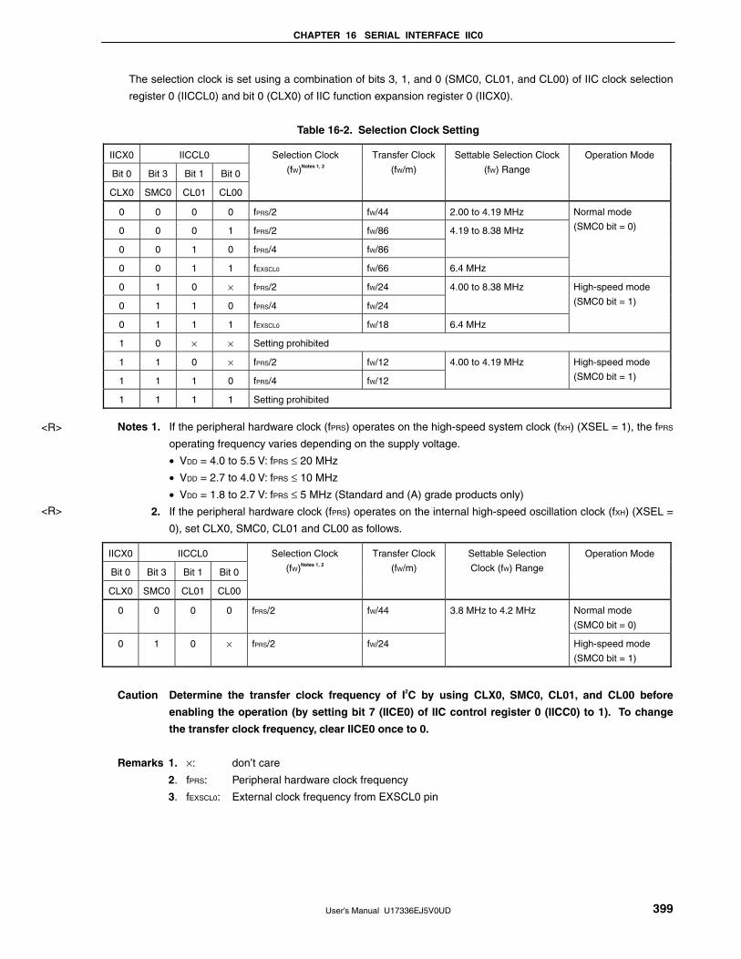
CHAPTER 16 SERIAL INTERFACE IIC0
User’s Manual U17336EJ5V0UD 399
The selection clock is set using a combination of bits 3, 1, and 0 (SMC0, CL01, and CL00) of IIC clock selection
register 0 (IICCL0) and bit 0 (CLX0) of IIC function expansion register 0 (IICX0).
Table 16-2. Selection Clock Setting
IICX0 IICCL0
Bit 0 Bit 3 Bit 1 Bit 0
CLX0 SMC0 CL01 CL00
Selection Clock
(fW)Notes 1, 2
Transfer Clock
(fW/m)
Settable Selection Clock
(fW) Range
Operation Mode
0 0 0 0 fPRS/2 fW/44 2.00 to 4.19 MHz
0 0 0 1 fPRS/2 fW/86
0 0 1 0 fPRS/4 fW/86
4.19 to 8.38 MHz
0 0 1 1 fEXSCL0 fW/66 6.4 MHz
Normal mode
(SMC0 bit = 0)
0 1 0 × fPRS/2 fW/24
0 1 1 0 fPRS/4 fW/24
4.00 to 8.38 MHz
0 1 1 1 fEXSCL0 fW/18 6.4 MHz
High-speed mode
(SMC0 bit = 1)
1 0 × × Setting prohibited
1 1 0 × fPRS/2 fW/12
1 1 1 0 fPRS/4 fW/12
4.00 to 4.19 MHz High-speed mode
(SMC0 bit = 1)
1 1 1 1 Setting prohibited
Notes 1. If the peripheral hardware clock (fPRS) operates on the high-speed system clock (fXH) (XSEL = 1), the fPRS
operating frequency varies depending on the supply voltage.
• VDD = 4.0 to 5.5 V: fPRS ≤ 20 MHz
• VDD = 2.7 to 4.0 V: fPRS ≤ 10 MHz
• VDD = 1.8 to 2.7 V: fPRS ≤ 5 MHz (Standard and (A) grade products only)
2. If the peripheral hardware clock (fPRS) operates on the internal high-speed oscillation clock (fXH) (XSEL =
0), set CLX0, SMC0, CL01 and CL00 as follows.
IICX0 IICCL0
Bit 0 Bit 3 Bit 1 Bit 0
CLX0 SMC0 CL01 CL00
Selection Clock
(fW)Notes 1, 2
Transfer Clock
(fW/m)
Settable Selection
Clock (fW) Range
Operation Mode
0 0 0 0 fPRS/2 fW/44 Normal mode
(SMC0 bit = 0)
0 1 0 × fPRS/2 fW/24
3.8 MHz to 4.2 MHz
High-speed mode
(SMC0 bit = 1)
Caution Determine the transfer clock frequency of I2C by using CLX0, SMC0, CL01, and CL00 before
enabling the operation (by setting bit 7 (IICE0) of IIC control register 0 (IICC0) to 1). To change
the transfer clock frequency, clear IICE0 once to 0.
Remarks 1. ×: don’t care
2. fPRS: Peripheral hardware clock frequency
3. fEXSCL0: External clock frequency from EXSCL0 pin
<R>
<R>

CHAPTER 16 SERIAL INTERFACE IIC0
User’s Manual U17336EJ5V0UD 400
(7) Port mode register 6 (PM6)
This register sets the input/output of port 6 in 1-bit units.
When using the P60/SCL0 pin as clock I/O and the P61/SDA0 pin as serial data I/O, clear PM60 and PM61,
and the output latches of P60 and P61 to 0.
Set IICE0 (bit 7 of IIC control register 0 (IICC0)) to 1 before setting the output mode because the P60/SCL0
and P61/SDA0 pins output a low level (fixed) when IICE0 is 0.
PM6 is set by a 1-bit or 8-bit memory manipulation instruction.
Reset signal generation sets PM6 to FFH.
Figure 16-10. Format of Port Mode Register 6 (PM6)
PM60PM61PM62PM631111
P6n pin I/O mode selection (n = 0 to 3)
Output mode (output buffer on)
Input mode (output buffer off)
PM6n
0
1
01234567
PM6
Address: FF26H After reset: FFH R/W
Symbol

CHAPTER 16 SERIAL INTERFACE IIC0
User’s Manual U17336EJ5V0UD 401
16.4 I2C Bus Mode Functions
16.4.1 Pin configuration
The serial clock pin (SCL0) and serial data bus pin (SDA0) are configured as follows.
(1) SCL0 ...... This pin is used for serial clock input and output.
This pin is an N-ch open-drain output for both master and slave devices. Input is Schmitt input.
(2) SDA0 ...... This pin is used for serial data input and output.
This pin is an N-ch open-drain output for both master and slave devices. Input is Schmitt input.
Since outputs from the serial clock line and the serial data bus line are N-ch open-drain outputs, an external pull-up
resistor is required.
Figure 16-11. Pin Configuration Diagram
Master device
Clock output
(Clock input)
Data output
Data input
VSS
VSS
SCL0
SDA0
VDD
VDD
(Clock output)
Clock input
Data output
Data input
VSS
VSS
Slave device
SCL0
SDA0

CHAPTER 16 SERIAL INTERFACE IIC0
User’s Manual U17336EJ5V0UD 402
16.5 I2C Bus Definitions and Control Methods
The following section describes the I2C bus’s serial data communication format and the signals used by the I2C bus.
Figure 16-12 shows the transfer timing for the “start condition”, “address”, “data”, and “stop condition” output via the
I2C bus’s serial data bus.
Figure 16-12. I2C Bus Serial Data Transfer Timing
SCL0
SDA0
Startcondition
Address R/W ACK Data
1-7 8 9 1-8
ACK Data ACK Stop condition
9 1-8 9
The master device generates the start condition, slave address, and stop condition.
The acknowledge (ACK) can be generated by either the master or slave device (normally, it is output by the device
that receives 8-bit data).
The serial clock (SCL0) is continuously output by the master device. However, in the slave device, the SCL0’s low
level period can be extended and a wait can be inserted.
16.5.1 Start conditions
A start condition is met when the SCL0 pin is at high level and the SDA0 pin changes from high level to low level.
The start conditions for the SCL0 pin and SDA0 pin are signals that the master device generates to the slave device
when starting a serial transfer. When the device is used as a slave, start conditions can be detected.
Figure 16-13. Start Conditions
SCL0
SDA0
H
A start condition is output when bit 1 (STT0) of IIC control register 0 (IICC0) is set (to 1) after a stop condition has
been detected (SPD0: Bit 0 = 1 in IIC status register 0 (IICS0)). When a start condition is detected, bit 1 (STD0) of
IICS0 is set (to 1).

CHAPTER 16 SERIAL INTERFACE IIC0
User’s Manual U17336EJ5V0UD 403
16.5.2 Addresses
The address is defined by the 7 bits of data that follow the start condition.
An address is a 7-bit data segment that is output in order to select one of the slave devices that are connected to
the master device via the bus lines. Therefore, each slave device connected via the bus lines must have a unique
address.
The slave devices include hardware that detects the start condition and checks whether or not the 7-bit address
data matches the data values stored in slave address register 0 (SVA0). If the address data matches the SVA0
values, the slave device is selected and communicates with the master device until the master device generates a
start condition or stop condition.
Figure 16-14. Address
SCL0
SDA0
INTIIC0
1 2 3 4 5 6 7 8 9
A6 A5 A4 A3 A2 A1 A0 R/W
Address
Note
Note INTIIC0 is not issued if data other than a local address or extension code is received during slave device
operation.
The slave address and the eighth bit, which specifies the transfer direction as described in 16.5.3 Transfer
direction specification below, are together written to IIC shift register 0 (IIC0) and are then output. Received
addresses are written to IIC0.
The slave address is assigned to the higher 7 bits of IIC0.
16.5.3 Transfer direction specification
In addition to the 7-bit address data, the master device sends 1 bit that specifies the transfer direction.
When this transfer direction specification bit has a value of “0”, it indicates that the master device is transmitting
data to a slave device. When the transfer direction specification bit has a value of “1”, it indicates that the master
device is receiving data from a slave device.
Figure 16-15. Transfer Direction Specification
SCL0
SDA0
INTIIC0
1 2 3 4 5 6 7 8 9
A6 A5 A4 A3 A2 A1 A0 R/W
Transfer direction specification
Note
Note INTIIC0 is not issued if data other than a local address or extension code is received during slave device
operation.

CHAPTER 16 SERIAL INTERFACE IIC0
User’s Manual U17336EJ5V0UD 404
16.5.4 ACK
ACK is used to check the status of serial data at the transmission and reception sides.
The reception side returns ACK each time it has received 8-bit data.
The transmission side usually receives ACK after transmitting 8-bit data. When ACK is returned from the reception
side, it is assumed that reception has been correctly performed and processing is continued. Whether ACK has been
detected can be checked by using bit 2 (ACKD0) of IIC status register 0 (IICS0).
When the master receives the last data item, it does not return ACK and instead generates a stop condition. If a
slave does not return ACK after receiving data, the master outputs a stop condition or restart condition and stops
transmission. If ACK is not returned, the possible causes are as follows.
<1> Reception was not performed normally.
<2> The final data item was received.
<3> The reception side specified by the address does not exist.
To generate ACK, the reception side makes the SDA0 line low at the ninth clock (indicating normal reception).
Automatic generation of ACK is enabled by setting bit 2 (ACKE0) of IIC control register 0 (IICC0) to 1. Bit 3 (TRC0)
of the IICS0 register is set by the data of the eighth bit that follows 7-bit address information. Usually, set ACKE0 to 1
for reception (TRC0 = 0).
If a slave can receive no more data during reception (TRC0 = 0) or does not require the next data item, then the
slave must inform the master, by clearing ACKE0 to 0, that it will not receive any more data.
When the master does not require the next data item during reception (TRC0 = 0), it must clear ACKE0 to 0 so that
ACK is not generated. In this way, the master informs a slave at the transmission side that it does not require any
more data (transmission will be stopped).
Figure 16-16. ACK
SCL0
SDA0
1 2 3 4 5 6 7 8 9
A6 A5 A4 A3 A2 A1 A0 R/W ACK
When the local address is received, ACK is automatically generated, regardless of the value of ACKE0. When an
address other than that of the local address is received, ACK is not generated (NACK).
When an extension code is received, ACK is generated if ACKE0 is set to 1 in advance.
How ACK is generated when data is received differs as follows depending on the setting of the wait timing.
• When 8-clock wait state is selected (bit 3 (WTIM0) of IICC0 register = 0):
By setting ACKE0 to 1 before releasing the wait state, ACK is generated at the falling edge of the eighth clock of
the SCL0 pin.
• When 9-clock wait state is selected (bit 3 (WTIM0) of IICC0 register = 1):
ACK is generated by setting ACKE0 to 1 in advance.

CHAPTER 16 SERIAL INTERFACE IIC0
User’s Manual U17336EJ5V0UD 405
16.5.5 Stop condition
When the SCL0 pin is at high level, changing the SDA0 pin from low level to high level generates a stop condition.
A stop condition is a signal that the master device generates to the slave device when serial transfer has been
completed. When the device is used as a slave, stop conditions can be detected.
Figure 16-17. Stop Condition
SCL0
SDA0
H
A stop condition is generated when bit 0 (SPT0) of IIC control register 0 (IICC0) is set to 1. When the stop
condition is detected, bit 0 (SPD0) of IIC status register 0 (IICS0) is set to 1 and INTIIC0 is generated when bit 4
(SPIE0) of IICC0 is set to 1.

CHAPTER 16 SERIAL INTERFACE IIC0
User’s Manual U17336EJ5V0UD 406
16.5.6 Wait
The wait is used to notify the communication partner that a device (master or slave) is preparing to transmit or
receive data (i.e., is in a wait state).
Setting the SCL0 pin to low level notifies the communication partner of the wait state. When wait state has been
canceled for both the master and slave devices, the next data transfer can begin.
Figure 16-18. Wait (1/2)
(1) When master device has a nine-clock wait and slave device has an eight-clock wait
(master transmits, slave receives, and ACKE0 = 1)
Master
IIC0
SCL0
Slave
IIC0
SCL0
ACKE0
Transfer lines
SCL0
SDA0
6 7 8 9 1 2 3
Master returns to highimpedance but slaveis in wait state (low level).
Wait after outputof ninth clock
IIC0 data write (cancel wait)
Wait after outputof eighth clock
Wait from slave Wait from master
FFH is written to IIC0 or WREL0 is set to 1
6 7 8 9 1 2 3
D2 D1 D0 D7 D6 D5ACK
H


CHAPTER 16 SERIAL INTERFACE IIC0
User’s Manual U17336EJ5V0UD 408
16.5.7 Canceling wait
The I2C usually cancels a wait state by the following processing.
• Writing data to IIC shift register 0 (IIC0)
• Setting bit 5 (WREL0) of IIC control register 0 (IICC0) (canceling wait)
• Setting bit 1 (STT0) of IIC0 register (generating start condition)Note
• Setting bit 0 (SPT0) of IIC0 register (generating stop condition)Note
Note Master only
When the above wait canceling processing is executed, the I2C cancels the wait state and communication is
resumed.
To cancel a wait state and transmit data (including addresses), write the data to IIC0.
To receive data after canceling a wait state, or to complete data transmission, set bit 5 (WREL0) of the IIC0 control
register 0 (IICC0) to 1.
To generate a restart condition after canceling a wait state, set bit 1 (STT0) of IICC0 to 1.
To generate a stop condition after canceling a wait state, set bit 0 (SPT0) of IICC0 to 1.
Execute the canceling processing only once for one wait state.
If, for example, data is written to IIC0 after canceling a wait state by setting WREL0 to 1, an incorrect value may be
output to SDA0 because the timing for changing the SDA0 line conflicts with the timing for writing IIC0.
In addition to the above, communication is stopped if IICE0 is cleared to 0 when communication has been aborted,
so that the wait state can be canceled.
If the I2C bus has deadlocked due to noise, processing is saved from communication by setting bit 6 (LREL0) of
IICC0, so that the wait state can be canceled.
16.5.8 Interrupt request (INTIIC0) generation timing and wait control
The setting of bit 3 (WTIM0) of IIC control register 0 (IICC0) determines the timing by which INTIIC0 is generated
and the corresponding wait control, as shown in Table 16-3.
Table 16-3. INTIIC0 Generation Timing and Wait Control
During Slave Device Operation During Master Device Operation WTIM0
Address Data Reception Data Transmission Address Data Reception Data Transmission
0 9Notes 1, 2 8Note 2 8Note 2 9 8 8
1 9Notes 1, 2 9Note 2 9Note 2 9 9 9
Notes 1. The slave device’s INTIIC0 signal and wait period occurs at the falling edge of the ninth clock only when
there is a match with the address set to slave address register 0 (SVA0).
At this point, ACK is generated regardless of the value set to IICC0’s bit 2 (ACKE0). For a slave device
that has received an extension code, INTIIC0 occurs at the falling edge of the eighth clock.
However, if the address does not match after restart, INTIIC0 is generated at the falling edge of the 9th
clock, but wait does not occur.
2. If the received address does not match the contents of slave address register 0 (SVA0) and extension
code is not received, neither INTIIC0 nor a wait occurs.
Remark The numbers in the table indicate the number of the serial clock’s clock signals. Interrupt requests and
wait control are both synchronized with the falling edge of these clock signals.

CHAPTER 16 SERIAL INTERFACE IIC0
User’s Manual U17336EJ5V0UD 409
(1) During address transmission/reception
• Slave device operation: Interrupt and wait timing are determined depending on the conditions described in
Notes 1 and 2 above, regardless of the WTIM0 bit.
• Master device operation: Interrupt and wait timing occur at the falling edge of the ninth clock regardless of
the WTIM0 bit.
(2) During data reception
• Master/slave device operation: Interrupt and wait timing are determined according to the WTIM0 bit.
(3) During data transmission
• Master/slave device operation: Interrupt and wait timing are determined according to the WTIM0 bit.
(4) Wait cancellation method
The four wait cancellation methods are as follows.
• Writing data to IIC shift register 0 (IIC0)
• Setting bit 5 (WREL0) of IIC control register 0 (IICC0) (canceling wait)
• Setting bit 1 (STT0) of IIC0 register (generating start condition)Note
• Setting bit 0 (SPT0) of IIC0 register (generating stop condition)Note
Note Master only.
When an 8-clock wait has been selected (WTIM0 = 0), the presence/absence of ACK generation must be
determined prior to wait cancellation.
(5) Stop condition detection
INTIIC0 is generated when a stop condition is detected (only when SPIE0 = 1).
16.5.9 Address match detection method
In I2C bus mode, the master device can select a particular slave device by transmitting the corresponding slave
address.
Address match can be detected automatically by hardware. An interrupt request (INTIIC0) occurs when a local
address has been set to slave address register 0 (SVA0) and when the address set to SVA0 matches the slave
address sent by the master device, or when an extension code has been received.
16.5.10 Error detection
In I2C bus mode, the status of the serial data bus (SDA0) during data transmission is captured by IIC shift register 0
(IIC0) of the transmitting device, so the IIC0 data prior to transmission can be compared with the transmitted IIC0 data
to enable detection of transmission errors. A transmission error is judged as having occurred when the compared
data values do not match.

CHAPTER 16 SERIAL INTERFACE IIC0
User’s Manual U17336EJ5V0UD 410
16.5.11 Extension code
(1) When the higher 4 bits of the receive address are either “0000” or “1111”, the extension code reception flag
(EXC0) is set to 1 for extension code reception and an interrupt request (INTIIC0) is issued at the falling edge
of the eighth clock. The local address stored in slave address register 0 (SVA0) is not affected.
(2) If “11110××0” is set to SVA0 by a 10-bit address transfer and “11110××0” is transferred from the master device,
the results are as follows. Note that INTIIC0 occurs at the falling edge of the eighth clock.
• Higher four bits of data match: EXC0 = 1
• Seven bits of data match: COI0 = 1
Remark EXC0: Bit 5 of IIC status register 0 (IICS0)
COI0: Bit 4 of IIC status register 0 (IICS0)
(3) Since the processing after the interrupt request occurs differs according to the data that follows the extension
code, such processing is performed by software.
If the extension code is received while a slave device is operating, then the slave device is participating in
communication even if its address does not match.
For example, after the extension code is received, if you do not wish to operate the target device as a slave
device, set bit 6 (LREL0) of the IIC control register 0 (IICC0) to 1 to set the standby mode for the next
communication operation.
Table 16-4. Extension Code Bit Definitions
Slave Address R/W Bit Description
0 0 0 0 0 0 0 0 General call address
0 0 0 0 0 0 0 1 Start byte
0 0 0 0 0 0 1 × C-BUS address
0 0 0 0 0 1 0 × Address that is reserved for different bus format
1 1 1 1 0 X X × 10-bit slave address specification
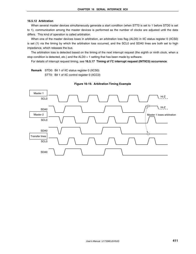
CHAPTER 16 SERIAL INTERFACE IIC0
User’s Manual U17336EJ5V0UD 411
16.5.12 Arbitration
When several master devices simultaneously generate a start condition (when STT0 is set to 1 before STD0 is set
to 1), communication among the master devices is performed as the number of clocks are adjusted until the data
differs. This kind of operation is called arbitration.
When one of the master devices loses in arbitration, an arbitration loss flag (ALD0) in IIC status register 0 (IICS0)
is set (1) via the timing by which the arbitration loss occurred, and the SCL0 and SDA0 lines are both set to high
impedance, which releases the bus.
The arbitration loss is detected based on the timing of the next interrupt request (the eighth or ninth clock, when a
stop condition is detected, etc.) and the ALD0 = 1 setting that has been made by software.
For details of interrupt request timing, see 16.5.17 Timing of I2C interrupt request (INTIIC0) occurrence.
Remark STD0: Bit 1 of IIC status register 0 (IICS0)
STT0: Bit 1 of IIC control register 0 (IICC0)
Figure 16-19. Arbitration Timing Example
SCL0
SDA0
SCL0
SDA0
SCL0
SDA0
Hi-Z
Hi-Z
Master 1 loses arbitration
Master 1
Master 2
Transfer lines

CHAPTER 16 SERIAL INTERFACE IIC0
User’s Manual U17336EJ5V0UD 412
Table 16-5. Status During Arbitration and Interrupt Request Generation Timing
Status During Arbitration Interrupt Request Generation Timing
During address transmission
Read/write data after address transmission
During extension code transmission
Read/write data after extension code transmission
During data transmission
During ACK transfer period after data transmission
When restart condition is detected during data transfer
At falling edge of eighth or ninth clock following byte transferNote 1
When stop condition is detected during data transfer When stop condition is generated (when SPIE0 = 1)Note 2
When data is at low level while attempting to generate a restart
condition
At falling edge of eighth or ninth clock following byte transferNote 1
When stop condition is detected while attempting to generate a
restart condition
When stop condition is generated (when SPIE0 = 1)Note 2
When data is at low level while attempting to generate a stop
condition
When SCL0 is at low level while attempting to generate a
restart condition
At falling edge of eighth or ninth clock following byte transferNote 1
Notes 1. When WTIM0 (bit 3 of IIC control register 0 (IICC0)) = 1, an interrupt request occurs at the falling edge
of the ninth clock. When WTIM0 = 0 and the extension code’s slave address is received, an interrupt
request occurs at the falling edge of the eighth clock.
2. When there is a chance that arbitration will occur, set SPIE0 = 1 for master device operation.
Remark SPIE0: Bit 4 of IIC control register 0 (IICC0)
16.5.13 Wakeup function
The I2C bus slave function is a function that generates an interrupt request signal (INTIIC0) when a local address
and extension code have been received.
This function makes processing more efficient by preventing unnecessary INTIIC0 signal from occurring when
addresses do not match.
When a start condition is detected, wakeup standby mode is set. This wakeup standby mode is in effect while
addresses are transmitted due to the possibility that an arbitration loss may change the master device (which has
generated a start condition) to a slave device.
However, when a stop condition is detected, bit 4 (SPIE0) of IIC control register 0 (IICC0) is set regardless of the
wakeup function, and this determines whether interrupt requests are enabled or disabled.

CHAPTER 16 SERIAL INTERFACE IIC0
User’s Manual U17336EJ5V0UD 413
16.5.14 Communication reservation
(1) When communication reservation function is enabled (bit 0 (IICRSV) of IIC flag register 0 (IICF0) = 0)
To start master device communications when not currently using a bus, a communication reservation can be
made to enable transmission of a start condition when the bus is released. There are two modes under which
the bus is not used.
• When arbitration results in neither master nor slave operation
• When an extension code is received and slave operation is disabled (ACK is not returned and the bus was
released when bit 6 (LREL0) of IIC control register 0 (IICC0) was set to 1).
If bit 1 (STT0) of IICC0 is set to 1 while the bus is not used (after a stop condition is detected), a start condition
is automatically generated and wait state is set.
If an address is written to IIC shift register 0 (IIC0) after bit 4 (SPIE0) of IICC0 was set to 1, and it was detected
by generation of an interrupt request signal (INTIIC0) that the bus was released (detection of the stop
condition), then the device automatically starts communication as the master. Data written to IIC0 before the
stop condition is detected is invalid.
When STT0 has been set to 1, the operation mode (as start condition or as communication reservation) is
determined according to the bus status.
• If the bus has been released.........................................a start condition is generated
• If the bus has not been released (standby mode) .........communication reservation
Check whether the communication reservation operates or not by using MSTS0 (bit 7 of IIC status register 0
(IICS0)) after STT0 is set to 1 and the wait time elapses.
The wait periods, which should be set via software, are listed in Table 16-6.
Table 16-6. Wait Periods
CLX0 SMC0 CL01 CL00 Wait Period
0 0 0 0 46 clocks
0 0 0 1 86 clocks
0 0 1 0 172 clocks
0 0 1 1 34 clocks
0 1 0 0
0 1 0 1
30 clocks
0 1 1 0 60 clocks
0 1 1 1 12 clocks
1 1 0 0
1 1 0 1
18 clocks
1 1 1 0 36 clocks
Figure 16-20 shows the communication reservation timing.

CHAPTER 16 SERIAL INTERFACE IIC0
User’s Manual U17336EJ5V0UD 414
Figure 16-20. Communication Reservation Timing
21 3 4 5 6 21 3 4 5 67 8 9SCL0
SDA0
Program processing
Hardware processing
Write toIIC0
Set SPD0and INTIIC0
STT0 = 1
Communi-cationreservation
SetSTD0
Generate by master device with bus mastership
Remark IIC0: IIC shift register 0
STT0: Bit 1 of IIC control register 0 (IICC0)
STD0: Bit 1 of IIC status register 0 (IICS0)
SPD0: Bit 0 of IIC status register 0 (IICS0)
Communication reservations are accepted via the following timing. After bit 1 (STD0) of IIC status register 0
(IICS0) is set to 1, a communication reservation can be made by setting bit 1 (STT0) of IIC control register 0
(IICC0) to 1 before a stop condition is detected.
Figure 16-21. Timing for Accepting Communication Reservations
SCL0
SDA0
STD0
SPD0
Standby mode
Figure 16-22 shows the communication reservation protocol.

CHAPTER 16 SERIAL INTERFACE IIC0
User’s Manual U17336EJ5V0UD 415
Figure 16-22. Communication Reservation Protocol
DI
SET1 STT0
Define communicationreservation
Wait
MSTS0 = 0? (Communication reservation)Note
Yes
No
(Generate start condition)
Cancel communicationreservation
MOV IIC0, #××H
EI
Sets STT0 flag (communication reservation)
Defines that communication reservation is in effect(defines and sets user flag to any part of RAM)
Secures wait period set by software (see Table 16-6).
Confirmation of communication reservation
Clear user flag
IIC0 write operation
Note The communication reservation operation executes a write to IIC shift register 0 (IIC0) when a stop
condition interrupt request occurs.
Remark STT0: Bit 1 of IIC control register 0 (IICC0)
MSTS0: Bit 7 of IIC status register 0 (IICS0)
IIC0: IIC shift register 0
(2) When communication reservation function is disabled (bit 0 (IICRSV) of IIC flag register 0 (IICF0) = 1)
When bit 1 (STT0) of IIC control register 0 (IICC0) is set to 1 when the bus is not used in a communication
during bus communication, this request is rejected and a start condition is not generated. The following two
statuses are included in the status where bus is not used.
• When arbitration results in neither master nor slave operation
• When an extension code is received and slave operation is disabled (ACK is not returned and the bus was
released when bit 6 (LREL0) of IICC0 was set to 1)
To confirm whether the start condition was generated or request was rejected, check STCF (bit 7 of IICF0).
The time shown in Table 16-7 is required until STCF is set to 1 after setting STT0 = 1. Therefore, secure the
time by software.
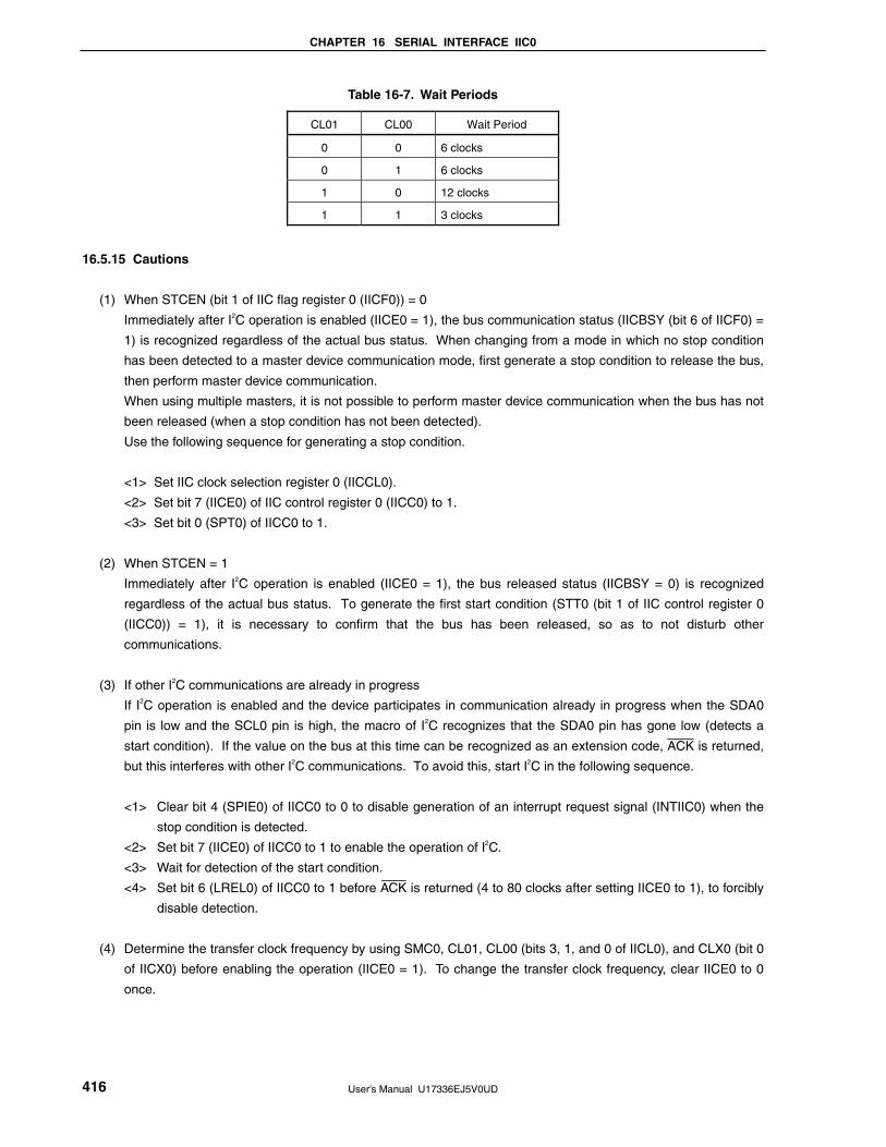
CHAPTER 16 SERIAL INTERFACE IIC0
User’s Manual U17336EJ5V0UD 416
Table 16-7. Wait Periods
CL01 CL00 Wait Period
0 0 6 clocks
0 1 6 clocks
1 0 12 clocks
1 1 3 clocks
16.5.15 Cautions
(1) When STCEN (bit 1 of IIC flag register 0 (IICF0)) = 0
Immediately after I2C operation is enabled (IICE0 = 1), the bus communication status (IICBSY (bit 6 of IICF0) =
1) is recognized regardless of the actual bus status. When changing from a mode in which no stop condition
has been detected to a master device communication mode, first generate a stop condition to release the bus,
then perform master device communication.
When using multiple masters, it is not possible to perform master device communication when the bus has not
been released (when a stop condition has not been detected).
Use the following sequence for generating a stop condition.
<1> Set IIC clock selection register 0 (IICCL0).
<2> Set bit 7 (IICE0) of IIC control register 0 (IICC0) to 1.
<3> Set bit 0 (SPT0) of IICC0 to 1.
(2) When STCEN = 1
Immediately after I2C operation is enabled (IICE0 = 1), the bus released status (IICBSY = 0) is recognized
regardless of the actual bus status. To generate the first start condition (STT0 (bit 1 of IIC control register 0
(IICC0)) = 1), it is necessary to confirm that the bus has been released, so as to not disturb other
communications.
(3) If other I2C communications are already in progress
If I2C operation is enabled and the device participates in communication already in progress when the SDA0
pin is low and the SCL0 pin is high, the macro of I2C recognizes that the SDA0 pin has gone low (detects a
start condition). If the value on the bus at this time can be recognized as an extension code, ACK is returned,
but this interferes with other I2C communications. To avoid this, start I2C in the following sequence.
<1> Clear bit 4 (SPIE0) of IICC0 to 0 to disable generation of an interrupt request signal (INTIIC0) when the
stop condition is detected.
<2> Set bit 7 (IICE0) of IICC0 to 1 to enable the operation of I2C.
<3> Wait for detection of the start condition.
<4> Set bit 6 (LREL0) of IICC0 to 1 before ACK is returned (4 to 80 clocks after setting IICE0 to 1), to forcibly
disable detection.
(4) Determine the transfer clock frequency by using SMC0, CL01, CL00 (bits 3, 1, and 0 of IICL0), and CLX0 (bit 0
of IICX0) before enabling the operation (IICE0 = 1). To change the transfer clock frequency, clear IICE0 to 0
once.

CHAPTER 16 SERIAL INTERFACE IIC0
User’s Manual U17336EJ5V0UD 417
(5) Setting STT0 and SPT0 (bits 1 and 0 of IICC0) again after they are set and before they are cleared to 0 is
prohibited.
(6) When transmission is reserved, set SPIE0 (bit 4 of IICL0) to 1 so that an interrupt request is generated when
the stop condition is detected. Transfer is started when communication data is written to IIC0 after the interrupt
request is generated. Unless the interrupt is generated when the stop condition is detected, the device stops
in the wait state because the interrupt request is not generated when communication is started. However, it is
not necessary to set SPIE0 to 1 when MSTS0 (bit 7 of IICS0) is detected by software.
16.5.16 Communication operations
The following shows three operation procedures with the flowchart.
(1) Master operation in single master system
The flowchart when using the 78K0/KC2 as the master in a single master system is shown below.
This flowchart is broadly divided into the initial settings and communication processing. Execute the initial
settings at startup. If communication with the slave is required, prepare the communication and then execute
communication processing.
(2) Master operation in multimaster system
In the I2C bus multimaster system, whether the bus is released or used cannot be judged by the I2C bus
specifications when the bus takes part in a communication. Here, when data and clock are at a high level for a
certain period (1 frame), the 78K0/KC2 takes part in a communication with bus released state.
This flowchart is broadly divided into the initial settings, communication waiting, and communication processing.
The processing when the 78K0/KC2 looses in arbitration and is specified as the slave is omitted here, and only
the processing as the master is shown. Execute the initial settings at startup to take part in a communication.
Then, wait for the communication request as the master or wait for the specification as the slave. The actual
communication is performed in the communication processing, and it supports the transmission/reception with
the slave and the arbitration with other masters.
(3) Slave operation
An example of when the 78K0/KC2 is used as the I2C bus slave is shown below.
When used as the slave, operation is started by an interrupt. Execute the initial settings at startup, then wait
for the INTIIC0 interrupt occurrence (communication waiting). When an INTIIC0 interrupt occurs, the
communication status is judged and its result is passed as a flag over to the main processing.
By checking the flags, necessary communication processing is performed.

CHAPTER 16 SERIAL INTERFACE IIC0
User’s Manual U17336EJ5V0UD 418
(1) Master operation in single-master system
Figure 16-23. Master Operation in Single-Master System
SPT0 = 1
SPT0 = 1
WREL0 = 1
START
END
ACKE0 = 0WTIM0 = WREL0 = 1
No
No
Yes
NoNo
No
Yes
YesYes
Yes
STCEN = 1?
ACKE0 = 1WTIM0 = 0
TRC0 = 1?
ACKD0 = 1?
ACKD0 = 1?
No
Yes
No
Yes
Yes
No
Yes
No
Yes
No
Yes
No
Yes
No
STT0 = 1
IICX0 ← 0XHIICCL0 ← XXH
IICF0 ← 0XHSetting STCEN, IICRSV = 0
IICC0 ← XXHACKE0 = WTIM0 = SPIE0 = 1
IICE0 = 1
Setting port
Initializing I2C busNote
SVA0 ← XXH
Writing IIC0
Writing IIC0
Reading IIC0
INTIIC0interrupt occurs?
End of transfer?End of transfer?
Restart?
Sets each pin in the I2C mode (see 16.3 (7) Port mode register 6 (PM6)).
Selects a transfer clock.
Sets a local address.
Sets a start condition.
Prepares for starting communication (generates a start condition).
Starts communication (specifies an address and transfer direction).
Waits for detection of acknowledge.
Waits for data transmission.
Starts transmission.
Com
mun
icat
ion
proc
essi
ngIn
itial
set
ting
Starts reception.
Waits for data reception.
INTIIC0interrupt occurs?
Waits for detection of acknowledge.
Prepares for starting communication (generates a stop condition).
Waits for detection of the stop condition.
INTIIC0Interrupt occurs?
INTIIC0interrupt occurs?
INTIIC0interrupt occurs?
Note Release (SCL0 and SDA0 pins = high level) the I2C bus in conformance with the specifications of the product that is communicating. If EEPROM is outputting a low level to the SDA0 pin, for example, set the
SCL0 pin in the output port mode, and output a clock pulse from the output port until the SDA0 pin is
constantly at high level.
Remark Conform to the specifications of the product that is communicating, with respect to the transmission and reception formats.

CHAPTER 16 SERIAL INTERFACE IIC0
User’s Manual U17336EJ5V0UD 419
(2) Master operation in multi-master system
Figure 16-24. Master Operation in Multi-Master System (1/3)
IICX0 ← 0XHIICCL0 ← XXH
IICF0 ← 0XHSetting STCEN and IICRSV
IICC0 ← XXHACKE0 = WTIM0 = SPIE0 = 1
IICE0 = 1
Setting port
SPT0 = 1
SVA0 ← XXH
SPIE0 = 1
START
Slave operation
Slave operation
Releases the bus for a specific period.
Bus status is being checked.
Yes
Checking bus statusNote
Master operationstarts?
Enables reservingcommunication.
Disables reservingcommunication.
SPD0 = 1?
STCEN = 1?
IICRSV = 0?
A
Sets each pin in the I2C mode (see 16.3 (7) Port mode register 6 (PM6)).
Selects a transfer clock.
Sets a local address.
Sets a start condition.
(Communication start request)
(No communication start request)
• Waiting to be specified as a slave by other master• Waiting for a communication start request (depends on user program)
Prepares for starting communication (generates a stop condition).
Waits for detection of the stop condition.
No
Yes
Yes
NoINTIIC0interrupt occurs?
INTIIC0interrupt occurs?
Yes
No Yes
No
SPD0 = 1?
Yes
NoSlave operation
No
INTIIC0interrupt occurs?
Yes
No
1
B
SPIE0 = 0
Yes
NoWaits for a communication request.
Wai
ts fo
r a
com
mun
icat
ion
Initi
al s
ettin
g
Note Confirm that the bus is released (CLD0 bit = 1, DAD0 bit = 1) for a specific period (for example, for a period
of one frame). If the SDA0 pin is constantly at low level, decide whether to release the I2C bus (SCL0 and
SDA0 pins = high level) in conformance with the specifications of the product that is communicating.

CHAPTER 16 SERIAL INTERFACE IIC0
User’s Manual U17336EJ5V0UD 420
Figure 16-24. Master Operation in Multi-Master System (2/3)
STT0 = 1
Wait
Slave operation
Yes
MSTS0 = 1?
EXC0 = 1 or COI0 =1?
Prepares for starting communication (generates a start condition).
Secure wait time by software (see Table 16-6).
Waits for bus release (communication being reserved).
Wait state after stop condition was detected and start condition was generated by the communication reservation function.
NoINTIIC0interrupt occurs?
Yes
Yes
No
No
A
C
STT0 = 1
Wait
Slave operation
Yes
IICBSY = 0?
EXC0 = 1 or COI0 =1?
Prepares for starting communication (generates a start condition).
Disables reserving communication.
Enables reserving communication.
Secure wait time by software (see Table 18-7).
Waits for bus release
Detects a stop condition.
No
No
INTIIC0interrupt occurs?
Yes
Yes
No
Yes
STCF = 0? No
B
D
C
D
Com
mun
icat
ion
proc
essi
ngC
omm
unic
atio
n pr
oces
sing

CHAPTER 16 SERIAL INTERFACE IIC0
User’s Manual U17336EJ5V0UD 421
Figure 16-24. Master Operation in Multi-Master System (3/3)
Writing IIC0
WTIM0 = 1
WREL0 = 1
Reading IIC0
ACKE0 = 1WTIM0 = 0
WTIM0 = WREL0 = 1ACKE0 = 0
Writing IIC0
Yes
TRC0 = 1?
Restart?
MSTS0 = 1?
Starts communication (specifies an address and transfer direction).
Starts transmission.
No
Yes
Waits for data reception.
Starts reception.
Yes
NoINTIIC0interrupt occurs?
Yes
NoTransfer end?
Waits for detection of ACK.
Yes
NoINTIIC0interrupt occurs?
Waits for data transmission.
Does not participate in communication.
Yes
NoINTIIC0interrupt occurs?
No
Yes
ACKD0 = 1?No
Yes
No
C
2
Yes
MSTS0 = 1? No
Yes
Transfer end?No
Yes
ACKD0 = 1? No
2
Yes
MSTS0 = 1? No
2
Waits for detection of ACK.
Yes
NoINTIIC0interrupt occurs?
Yes
MSTS0 = 1? No
C
2
Yes
EXC0 = 1 or COI0 = 1? No
1
2
SPT0 = 1
STT0 = 1
Slave operation
END
Com
mun
icat
ion
proc
essi
ngC
omm
unic
atio
n pr
oces
sing
Remarks 1. Conform to the specifications of the product that is communicating, with respect to the transmission
and reception formats.
2. To use the device as a master in a multi-master system, read the MSTS0 bit each time interrupt INTIIC0 has occurred to check the arbitration result.
3. To use the device as a slave in a multi-master system, check the status by using the IICS0 and IICF0
registers each time interrupt INTIIC0 has occurred, and determine the processing to be performed next.

CHAPTER 16 SERIAL INTERFACE IIC0
User’s Manual U17336EJ5V0UD 422
(3) Slave operation
The processing procedure of the slave operation is as follows.
Basically, the slave operation is event-driven. Therefore, processing by the INTIIC0 interrupt (processing that
must substantially change the operation status such as detection of a stop condition during communication) is
necessary.
In the following explanation, it is assumed that the extension code is not supported for data communication. It
is also assumed that the INTIIC0 interrupt servicing only performs status transition processing, and that actual
data communication is performed by the main processing.
IIC0
Interrupt servicing
Main processing
INTIIC0 Flag
Setting
Data
Setting
Therefore, data communication processing is performed by preparing the following three flags and passing
them to the main processing instead of INTIIC0.
<1> Communication mode flag
This flag indicates the following two communication statuses.
• Clear mode: Status in which data communication is not performed
• Communication mode: Status in which data communication is performed (from valid address detection
to stop condition detection, no detection of ACK from master, address
mismatch)
<2> Ready flag
This flag indicates that data communication is enabled. Its function is the same as the INTIIC0 interrupt
for ordinary data communication. This flag is set by interrupt servicing and cleared by the main
processing. Clear this flag by interrupt servicing when communication is started. However, the ready flag
is not set by interrupt servicing when the first data is transmitted. Therefore, the first data is transmitted
without the flag being cleared (an address match is interpreted as a request for the next data).
<3> Communication direction flag
This flag indicates the direction of communication. Its value is the same as TRC0.

CHAPTER 16 SERIAL INTERFACE IIC0
User’s Manual U17336EJ5V0UD 423
The main processing of the slave operation is explained next.
Start serial interface IIC0 and wait until communication is enabled. When communication is enabled, execute
communication by using the communication mode flag and ready flag (processing of the stop condition and
start condition is performed by an interrupt. Here, check the status by using the flags).
The transmission operation is repeated until the master no longer returns ACK. If ACK is not returned from the
master, communication is completed.
For reception, the necessary amount of data is received. When communication is completed, ACK is not
returned as the next data. After that, the master generates a stop condition or restart condition. Exit from the
communication status occurs in this way.
Figure 16-25. Slave Operation Flowchart (1)
Yes
Yes
Yes
Yes
Yes
Yes
Yes
No
No
No
No
No
No
WREL0 = 1
ACKD0 = 1?
No
Yes
No
Yes
No
START
Communicationmode flag = 1?
Communicationmode flag = 1?
Communicationdirection flag = 1?
Ready flag = 1?
Communicationdirection flag = 1?
Reading IIC0
Clearing ready flag
Clearing ready flag
Communicationdirection flag = 1?
Clearing communicationmode flag
WREL0 = 1
Writing IIC0
IICC0 ← XXHACKE0 = WTIM0 = 1SPIE0 = 0, IICE0 = 1
SVA0 ← XXH Sets a local address.
IICX0 ← 0XH
IICCL0 ← XXHSelects a transfer clock.
IICF0 ← 0XH
Setting IICRSVSets a start condition.
Starts transmission.
Starts reception.
Communicationmode flag = 1?
Ready flag = 1?
Setting port Sets each pin to the I2C mode (see 16.3 (7) Port mode register 6 (PM6)).
Com
mun
icat
ion
proc
essi
ngIn
itial
set
ting
Remark Conform to the specifications of the product that is in communication, regarding the transmission and
reception formats.

CHAPTER 16 SERIAL INTERFACE IIC0
User’s Manual U17336EJ5V0UD 424
An example of the processing procedure of the slave with the INTIIC0 interrupt is explained below (processing
is performed assuming that no extension code is used). The INTIIC0 interrupt checks the status, and the
following operations are performed.
<1> Communication is stopped if the stop condition is issued.
<2> If the start condition is issued, the address is checked and communication is completed if the address
does not match. If the address matches, the communication mode is set, wait is cancelled, and
processing returns from the interrupt (the ready flag is cleared).
<3> For data transmit/receive, only the ready flag is set. Processing returns from the interrupt with the I2C bus
remaining in the wait state.
Remark <1> to <3> above correspond to <1> to <3> in Figure 16-26 Slave Operation Flowchart (2).
Figure 16-26. Slave Operation Flowchart (2)
Yes
Yes
Yes
NoNo
No
INTIIC0 generated
Set ready flag
Interrupt servicing completed
SPD0 = 1?
STD0 = 1?
COI0 = 1?
Communication direction flag← TRC0
Set communication mode flagClear ready flag
Clear communication direction flag, ready flag, and
communication mode flag
<1>
<2>
<3>

CHAPTER 16 SERIAL INTERFACE IIC0
User’s Manual U17336EJ5V0UD 425
16.5.17 Timing of I2C interrupt request (INTIIC0) occurrence
The timing of transmitting or receiving data and generation of interrupt request signal INTIIC0, and the value of the
IICS0 register when the INTIIC0 signal is generated are shown below.
Remark ST: Start condition
AD6 to AD0: Address
R/W: Transfer direction specification
ACK: Acknowledge
D7 to D0: Data
SP: Stop condition
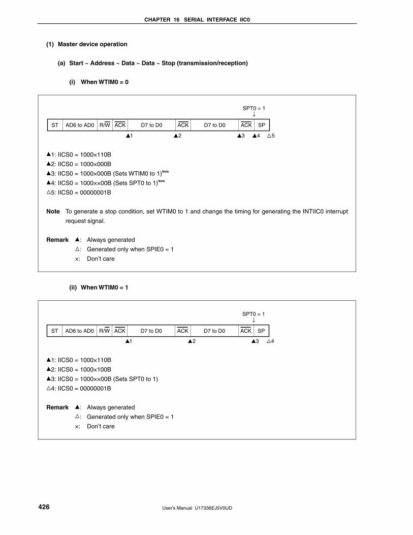
CHAPTER 16 SERIAL INTERFACE IIC0
User’s Manual U17336EJ5V0UD 426
(1) Master device operation
(a) Start ~ Address ~ Data ~ Data ~ Stop (transmission/reception)
(i) When WTIM0 = 0
ST AD6 to AD0 R/W ACK D7 to D0 D7 to D0ACK ACK SP
SPT0 = 1↓
3 4 5 2 1
1: IICS0 = 1000×110B
2: IICS0 = 1000×000B
3: IICS0 = 1000×000B (Sets WTIM0 to 1)Note
4: IICS0 = 1000××00B (Sets SPT0 to 1)Note
5: IICS0 = 00000001B
Note To generate a stop condition, set WTIM0 to 1 and change the timing for generating the INTIIC0 interrupt
request signal.
Remark : Always generated
: Generated only when SPIE0 = 1
×: Don’t care
(ii) When WTIM0 = 1
ST AD6 to AD0 R/W ACK D7 to D0 D7 to D0ACK ACK SP
SPT0 = 1↓
3 4 2 1
1: IICS0 = 1000×110B
2: IICS0 = 1000×100B
3: IICS0 = 1000××00B (Sets SPT0 to 1)
4: IICS0 = 00000001B
Remark : Always generated
: Generated only when SPIE0 = 1
×: Don’t care
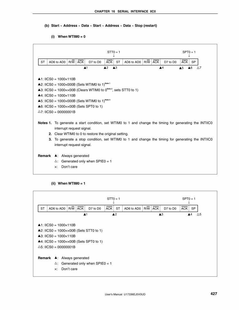
CHAPTER 16 SERIAL INTERFACE IIC0
User’s Manual U17336EJ5V0UD 427
(b) Start ~ Address ~ Data ~ Start ~ Address ~ Data ~ Stop (restart)
(i) When WTIM0 = 0
ST AD6 to AD0 R/W ACK D7 to D0 AD6 to AD0ACK ACK SPST R/W D7 to D0 ACK
STT0 = 1↓
SPT0 = 1↓
3 4 7 2 1 5 6
1: IICS0 = 1000×110B
2: IICS0 = 1000×000B (Sets WTIM0 to 1)Note 1
3: IICS0 = 1000××00B (Clears WTIM0 to 0Note 2, sets STT0 to 1)
4: IICS0 = 1000×110B
5: IICS0 = 1000×000B (Sets WTIM0 to 1)Note 3
6: IICS0 = 1000××00B (Sets SPT0 to 1)
7: IICS0 = 00000001B
Notes 1. To generate a start condition, set WTIM0 to 1 and change the timing for generating the INTIIC0
interrupt request signal.
2. Clear WTIM0 to 0 to restore the original setting.
3. To generate a stop condition, set WTIM0 to 1 and change the timing for generating the INTIIC0
interrupt request signal.
Remark : Always generated
: Generated only when SPIE0 = 1
×: Don’t care
(ii) When WTIM0 = 1
ST AD6 to AD0 R/W ACK D7 to D0 AD6 to AD0ACK ACK SPST R/W D7 to D0 ACK
STT0 = 1↓
SPT0 = 1↓
3 4 5 2 1
1: IICS0 = 1000×110B
2: IICS0 = 1000××00B (Sets STT0 to 1)
3: IICS0 = 1000×110B
4: IICS0 = 1000××00B (Sets SPT0 to 1)
5: IICS0 = 00000001B
Remark : Always generated
: Generated only when SPIE0 = 1
×: Don’t care

CHAPTER 16 SERIAL INTERFACE IIC0
User’s Manual U17336EJ5V0UD 428
(c) Start ~ Code ~ Data ~ Data ~ Stop (extension code transmission)
(i) When WTIM0 = 0
ST AD6 to AD0 R/W ACK D7 to D0 D7 to D0ACK ACK SP
SPT0 = 1↓
3 4 5 2 1
1: IICS0 = 1010×110B
2: IICS0 = 1010×000B
3: IICS0 = 1010×000B (Sets WTIM0 to 1)Note
4: IICS0 = 1010××00B (Sets SPT0 to 1)
5: IICS0 = 00000001B
Note To generate a stop condition, set WTIM0 to 1 and change the timing for generating the INTIIC0 interrupt
request signal.
Remark : Always generated
: Generated only when SPIE0 = 1
×: Don’t care
(ii) When WTIM0 = 1
ST AD6 to AD0 R/W ACK D7 to D0 D7 to D0ACK ACK SP
SPT0 = 1↓
3 4 2 1
1: IICS0 = 1010×110B
2: IICS0 = 1010×100B
3: IICS0 = 1010××00B (Sets SPT0 to 1)
4: IICS0 = 00001001B
Remark : Always generated
: Generated only when SPIE0 = 1
×: Don’t care

CHAPTER 16 SERIAL INTERFACE IIC0
User’s Manual U17336EJ5V0UD 429
(2) Slave device operation (slave address data reception)
(a) Start ~ Address ~ Data ~ Data ~ Stop
(i) When WTIM0 = 0
ST AD6 to AD0 R/W ACK D7 to D0 D7 to D0ACK ACK SP
3 4 2 1
1: IICS0 = 0001×110B
2: IICS0 = 0001×000B
3: IICS0 = 0001×000B
4: IICS0 = 00000001B
Remark : Always generated
: Generated only when SPIE0 = 1
×: Don’t care
(ii) When WTIM0 = 1
ST AD6 to AD0 R/W ACK D7 to D0 D7 to D0ACK ACK SP
3 4 2 1
1: IICS0 = 0001×110B
2: IICS0 = 0001×100B
3: IICS0 = 0001××00B
4: IICS0 = 00000001B
Remark : Always generated
: Generated only when SPIE0 = 1
×: Don’t care

CHAPTER 16 SERIAL INTERFACE IIC0
User’s Manual U17336EJ5V0UD 430
(b) Start ~ Address ~ Data ~ Start ~ Address ~ Data ~ Stop
(i) When WTIM0 = 0 (after restart, matches with SVA0)
ST AD6 to AD0 R/W ACK D7 to D0 AD6 to AD0ACK ACK SPST R/W D7 to D0 ACK
3 4 5 2 1
1: IICS0 = 0001×110B
2: IICS0 = 0001×000B
3: IICS0 = 0001×110B
4: IICS0 = 0001×000B
5: IICS0 = 00000001B
Remark : Always generated
: Generated only when SPIE0 = 1
×: Don’t care
(ii) When WTIM0 = 1 (after restart, matches with SVA0)
ST AD6 to AD0 R/W ACK D7 to D0 AD6 to AD0ACK ACK SPST R/W D7 to D0 ACK
3 4 5 2 1
1: IICS0 = 0001×110B
2: IICS0 = 0001××00B
3: IICS0 = 0001×110B
4: IICS0 = 0001××00B
5: IICS0 = 00000001B
Remark : Always generated
: Generated only when SPIE0 = 1
×: Don’t care
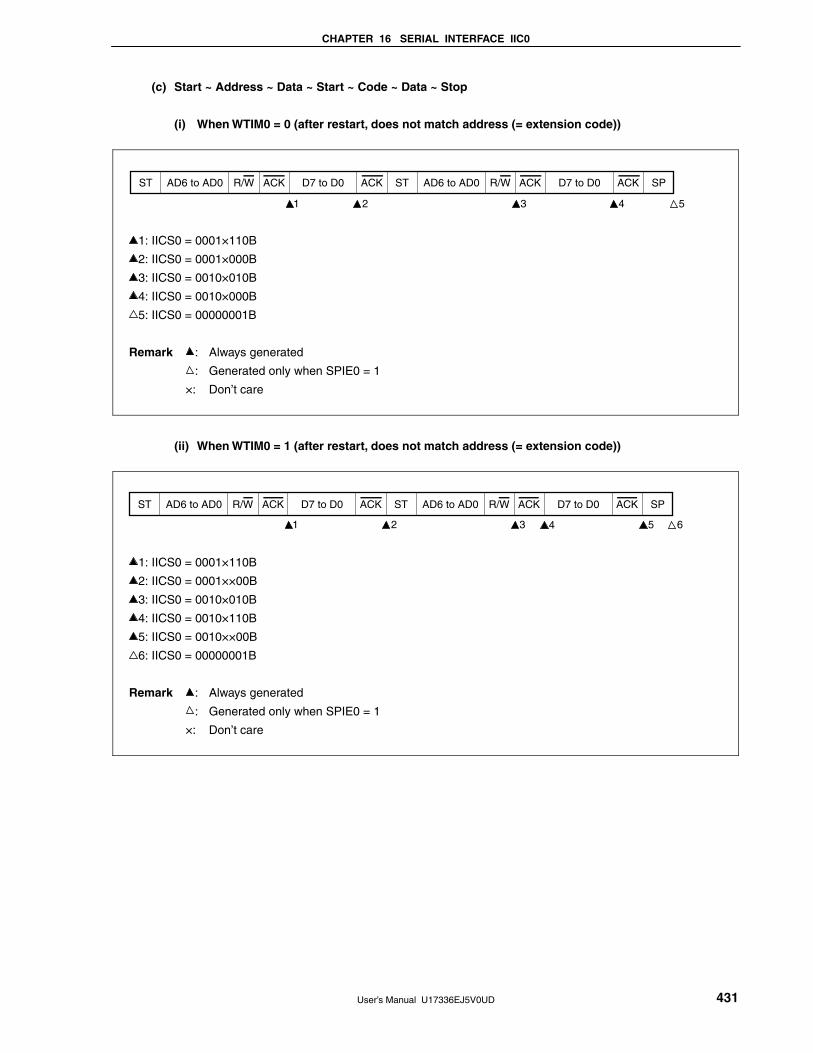
CHAPTER 16 SERIAL INTERFACE IIC0
User’s Manual U17336EJ5V0UD 431
(c) Start ~ Address ~ Data ~ Start ~ Code ~ Data ~ Stop
(i) When WTIM0 = 0 (after restart, does not match address (= extension code))
ST AD6 to AD0 R/W ACK D7 to D0 AD6 to AD0ACK ACK SPST R/W D7 to D0 ACK
3 4 5 2 1
1: IICS0 = 0001×110B
2: IICS0 = 0001×000B
3: IICS0 = 0010×010B
4: IICS0 = 0010×000B
5: IICS0 = 00000001B
Remark : Always generated
: Generated only when SPIE0 = 1
×: Don’t care
(ii) When WTIM0 = 1 (after restart, does not match address (= extension code))
ST AD6 to AD0 R/W ACK D7 to D0 AD6 to AD0ACK ACK SPST R/W D7 to D0 ACK
3 5 6 2 1 4
1: IICS0 = 0001×110B
2: IICS0 = 0001××00B
3: IICS0 = 0010×010B
4: IICS0 = 0010×110B
5: IICS0 = 0010××00B
6: IICS0 = 00000001B
Remark : Always generated
: Generated only when SPIE0 = 1
×: Don’t care

CHAPTER 16 SERIAL INTERFACE IIC0
User’s Manual U17336EJ5V0UD 432
(d) Start ~ Address ~ Data ~ Start ~ Address ~ Data ~ Stop
(i) When WTIM0 = 0 (after restart, does not match address (= not extension code))
ST AD6 to AD0 R/W ACK D7 to D0 AD6 to AD0ACK ACK SPST R/W D7 to D0 ACK
3 4 2 1
1: IICS0 = 0001×110B
2: IICS0 = 0001×000B
3: IICS0 = 00000110B
4: IICS0 = 00000001B
Remark : Always generated
: Generated only when SPIE0 = 1
×: Don’t care
(ii) When WTIM0 = 1 (after restart, does not match address (= not extension code))
ST AD6 to AD0 R/W ACK D7 to D0 AD6 to AD0ACK ACK SPST R/W D7 to D0 ACK
3 4 2 1
1: IICS0 = 0001×110B
2: IICS0 = 0001××00B
3: IICS0 = 00000110B
4: IICS0 = 00000001B
Remark : Always generated
: Generated only when SPIE0 = 1
×: Don’t care

CHAPTER 16 SERIAL INTERFACE IIC0
User’s Manual U17336EJ5V0UD 433
(3) Slave device operation (when receiving extension code)
The device is always participating in communication when it receives an extension code.
(a) Start ~ Code ~ Data ~ Data ~ Stop
(i) When WTIM0 = 0
ST AD6 to AD0 R/W ACK D7 to D0 D7 to D0ACK ACK SP
3 4 2 1
1: IICS0 = 0010×010B
2: IICS0 = 0010×000B
3: IICS0 = 0010×000B
4: IICS0 = 00000001B
Remark : Always generated
: Generated only when SPIE0 = 1
×: Don’t care
(ii) When WTIM0 = 1
ST AD6 to AD0 R/W ACK D7 to D0 D7 to D0ACK ACK SP
3 4 5 2 1
1: IICS0 = 0010×010B
2: IICS0 = 0010×110B
3: IICS0 = 0010×100B
4: IICS0 = 0010××00B
5: IICS0 = 00000001B
Remark : Always generated
: Generated only when SPIE0 = 1
×: Don’t care

CHAPTER 16 SERIAL INTERFACE IIC0
User’s Manual U17336EJ5V0UD 434
(b) Start ~ Code ~ Data ~ Start ~ Address ~ Data ~ Stop
(i) When WTIM0 = 0 (after restart, matches SVA0)
ST AD6 to AD0 R/W ACK D7 to D0 AD6 to AD0ACK ACK SPST R/W D7 to D0 ACK
3 4 5 2 1
1: IICS0 = 0010×010B
2: IICS0 = 0010×000B
3: IICS0 = 0001×110B
4: IICS0 = 0001×000B
5: IICS0 = 00000001B
Remark : Always generated
: Generated only when SPIE0 = 1
×: Don’t care
(ii) When WTIM0 = 1 (after restart, matches SVA0)
ST AD6 to AD0 R/W ACK D7 to D0 AD6 to AD0ACK ACK SPST R/W D7 to D0 ACK
3 4 6 2 1 5
1: IICS0 = 0010×010B
2: IICS0 = 0010×110B
3: IICS0 = 0010××00B
4: IICS0 = 0001×110B
5: IICS0 = 0001××00B
6: IICS0 = 00000001B
Remark : Always generated
: Generated only when SPIE0 = 1
×: Don’t care

CHAPTER 16 SERIAL INTERFACE IIC0
User’s Manual U17336EJ5V0UD 435
(c) Start ~ Code ~ Data ~ Start ~ Code ~ Data ~ Stop
(i) When WTIM0 = 0 (after restart, extension code reception)
ST AD6 to AD0 R/W ACK D7 to D0 AD6 to AD0ACK ACK SPST R/W D7 to D0 ACK
3 4 5 2 1
1: IICS0 = 0010×010B
2: IICS0 = 0010×000B
3: IICS0 = 0010×010B
4: IICS0 = 0010×000B
5: IICS0 = 00000001B
Remark : Always generated
: Generated only when SPIE0 = 1
×: Don’t care
(ii) When WTIM0 = 1 (after restart, extension code reception)
ST AD6 to AD0 R/W ACK D7 to D0 AD6 to AD0ACK ACK SPST R/W D7 to D0 ACK
3 4 7 2 1 5 6
1: IICS0 = 0010×010B
2: IICS0 = 0010×110B
3: IICS0 = 0010××00B
4: IICS0 = 0010×010B
5: IICS0 = 0010×110B
6: IICS0 = 0010××00B
7: IICS0 = 00000001B
Remark : Always generated

CHAPTER 16 SERIAL INTERFACE IIC0
User’s Manual U17336EJ5V0UD 436
(d) Start ~ Code ~ Data ~ Start ~ Address ~ Data ~ Stop
(i) When WTIM0 = 0 (after restart, does not match address (= not extension code))
ST AD6 to AD0 R/W ACK D7 to D0 AD6 to AD0ACK ACK SPST R/W D7 to D0 ACK
3 4 2 1
1: IICS0 = 00100010B
2: IICS0 = 00100000B
3: IICS0 = 00000110B
4: IICS0 = 00000001B
Remark : Always generated
: Generated only when SPIE0 = 1
×: Don’t care
(ii) When WTIM0 = 1 (after restart, does not match address (= not extension code))
ST AD6 to AD0 R/W ACK D7 to D0 AD6 to AD0ACK ACK SPST R/W D7 to D0 ACK
3 4 5 2 1
1: IICS0 = 00100010B
2: IICS0 = 00100110B
3: IICS0 = 00100×00B
4: IICS0 = 00000110B
5: IICS0 = 00000001B
Remark : Always generated
: Generated only when SPIE0 = 1
×: Don’t care

CHAPTER 16 SERIAL INTERFACE IIC0
User’s Manual U17336EJ5V0UD 437
(4) Operation without communication
(a) Start ~ Code ~ Data ~ Data ~ Stop
ST AD6 to AD0 R/W ACK D7 to D0 D7 to D0ACK ACK SP
1
1: IICS0 = 00000001B
Remark : Generated only when SPIE0 = 1
(5) Arbitration loss operation (operation as slave after arbitration loss)
When the device is used as a master in a multi-master system, read the MSTS0 bit each time interrupt request
signal INTIIC0 has occurred to check the arbitration result.
(a) When arbitration loss occurs during transmission of slave address data
(i) When WTIM0 = 0
ST AD6 to AD0 R/W ACK D7 to D0 D7 to D0ACK ACK SP
3 4 2 1
1: IICS0 = 0101×110B
2: IICS0 = 0001×000B
3: IICS0 = 0001×000B
4: IICS0 = 00000001B
Remark : Always generated
: Generated only when SPIE0 = 1
×: Don’t care

CHAPTER 16 SERIAL INTERFACE IIC0
User’s Manual U17336EJ5V0UD 438
(ii) When WTIM0 = 1
ST AD6 to AD0 R/W ACK D7 to D0 D7 to D0ACK ACK SP
3 4 2 1
1: IICS0 = 0101×110B
2: IICS0 = 0001×100B
3: IICS0 = 0001××00B
4: IICS0 = 00000001B
Remark : Always generated
: Generated only when SPIE0 = 1
×: Don’t care
(b) When arbitration loss occurs during transmission of extension code
(i) When WTIM0 = 0
ST AD6 to AD0 R/W ACK D7 to D0 D7 to D0ACK ACK SP
3 4 2 1
1: IICS0 = 0110×010B
2: IICS0 = 0010×000B
3: IICS0 = 0010×000B
4: IICS0 = 00000001B
Remark : Always generated
: Generated only when SPIE0 = 1
×: Don’t care

CHAPTER 16 SERIAL INTERFACE IIC0
User’s Manual U17336EJ5V0UD 439
(ii) When WTIM0 = 1
ST AD6 to AD0 R/W ACK D7 to D0 D7 to D0ACK ACK SP
3 4 5 2 1
1: IICS0 = 0110×010B
2: IICS0 = 0010×110B
3: IICS0 = 0010×100B
4: IICS0 = 0010××00B
5: IICS0 = 00000001B
Remark : Always generated
: Generated only when SPIE0 = 1
×: Don’t care
(6) Operation when arbitration loss occurs (no communication after arbitration loss)
When the device is used as a master in a multi-master system, read the MSTS0 bit each time interrupt request
signal INTIIC0 has occurred to check the arbitration result.
(a) When arbitration loss occurs during transmission of slave address data (when WTIM0 = 1)
ST AD6 to AD0 R/W ACK D7 to D0 D7 to D0ACK ACK SP
2 1
1: IICS0 = 01000110B
2: IICS0 = 00000001B
Remark : Always generated
: Generated only when SPIE0 = 1
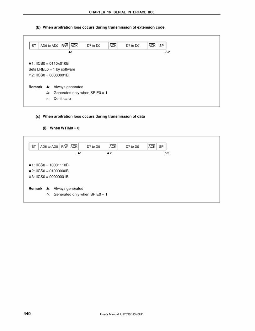
CHAPTER 16 SERIAL INTERFACE IIC0
User’s Manual U17336EJ5V0UD 440
(b) When arbitration loss occurs during transmission of extension code
ST AD6 to AD0 R/W ACK D7 to D0 D7 to D0ACK ACK SP
2 1
1: IICS0 = 0110×010B
Sets LREL0 = 1 by software
2: IICS0 = 00000001B
Remark : Always generated
: Generated only when SPIE0 = 1
×: Don’t care
(c) When arbitration loss occurs during transmission of data
(i) When WTIM0 = 0
ST AD6 to AD0 R/W ACK D7 to D0 D7 to D0ACK ACK SP
3 2 1
1: IICS0 = 10001110B
2: IICS0 = 01000000B
3: IICS0 = 00000001B
Remark : Always generated
: Generated only when SPIE0 = 1

CHAPTER 16 SERIAL INTERFACE IIC0
User’s Manual U17336EJ5V0UD 441
(ii) When WTIM0 = 1
ST AD6 to AD0 R/W ACK D7 to D0 D7 to D0ACK ACK SP
3 2 1
1: IICS0 = 10001110B
2: IICS0 = 01000100B
3: IICS0 = 00000001B
Remark : Always generated
: Generated only when SPIE0 = 1
(d) When loss occurs due to rest

CHAPTER 16 SERIAL INTERFACE IIC0
User’s Manual U17336EJ5V0UD 442
(ii) Extension code
ST AD6 to AD0 R/W ACK D7 to Dn AD6 to AD0 ACK SPST R/W D7 to D0 ACK
3 2 1
1: IICS0 = 1000×110B
2: IICS0 = 01100010B
Sets LREL0 = 1 by software
3: IICS0 = 00000001B
Remark : Always generated
: Generated only when SPIE0 = 1
×: Don’t care
n = 6 to 0
(e) When loss occurs due to stop condition during data transfer
ST AD6 to AD0 R/W ACK D7 to Dn SP
2 1
1: IICS0 = 10000110B
2: IICS0 = 01000001B
Remark : Always generated
: Generated only when SPIE0 = 1
×: Don’t care
n = 6 to 0

CHAPTER 16 SERIAL INTERFACE IIC0
User’s Manual U17336EJ5V0UD 443
(f) When arbitration loss occurs due to low-level data when attempting to generate a restart condition
(i) When WTIM0 = 0
ST AD6 to AD0 R/W ACK D7 to D0 D7 to D0ACK SPACK D7 to D0 ACK
STT0 = 1 ↓
3 4 5 2 1
1: IICS0 = 1000×110B
2: IICS0 = 1000×000B (Sets WTIM0 to 1)
3: IICS0 = 1000×100B (Clears WTIM0 to 0)
4: IICS0 = 01000000B
5: IICS0 = 00000001B
Remark : Always generated
: Generated only when SPIE0 = 1
×: Don’t care
(ii) When WTIM0 = 1
ST AD6 to AD0 R/W ACK D7 to D0 D7 to D0ACK SPACK D7 to D0 ACK
STT0 = 1 ↓
3 4 2 1
1: IICS0 = 1000×110B
2: IICS0 = 1000×100B (Sets STT0 to 1)
3: IICS0 = 01000100B
4: IICS0 = 00000001B
Remark : Always generated
: Generated only when SPIE0 = 1
×: Don’t care

CHAPTER 16 SERIAL INTERFACE IIC0
User’s Manual U17336EJ5V0UD 444
(g) When arbitration loss occurs due to a stop condition when attempting to generate a restart
condition
(i) When WTIM0 = 0
ST AD6 to AD0 R/W ACK D7 to D0 ACK SP
STT0 = 1 ↓
3 4 2 1
1: IICS0 = 1000×110B
2: IICS0 = 1000×000B (Sets WTIM0 to 1)
3: IICS0 = 1000××00B (Sets STT0 to 1)
4: IICS0 = 01000001B
Remark : Always generated
: Generated only when SPIE0 = 1
×: Don’t care
(ii) When WTIM0 = 1
ST AD6 to AD0 R/W ACK D7 to D0 ACK SP
STT0 = 1 ↓
2 3 1
1: IICS0 = 1000×110B
2: IICS0 = 1000××00B (Sets STT0 to 1)
3: IICS0 = 01000001B
Remark : Always generated
: Generated only when SPIE0 = 1
×: Don’t care

CHAPTER 16 SERIAL INTERFACE IIC0
User’s Manual U17336EJ5V0UD 445
(h) When arbitration loss occurs due to low-level data when attempting to generate a stop condition
(i) When WTIM0 = 0
ST AD6 to AD0 R/W ACK D7 to D0 D7 to D0ACK SPACK D7 to D0 ACK
SPT0 = 1 ↓
3 4 5 2 1
1: IICS0 = 1000×110B
2: IICS0 = 1000×000B (Sets WTIM0 to 1)
3: IICS0 = 1000×100B (Clears WTIM0 to 0)
4: IICS0 = 01000100B
5: IICS0 = 00000001B
Remark : Always generated
: Generated only when SPIE0 = 1
×: Don’t care
(ii) When WTIM0 = 1
ST AD6 to AD0 R/W ACK D7 to D0 D7 to D0ACK SPACK D7 to D0 ACK
SPT0 = 1 ↓
3 4 2 1
1: IICS0 = 1000×110B
2: IICS0 = 1000×100B (Sets SPT0 to 1)
3: IICS0 = 01000100B
4: IICS0 = 00000001B
Remark : Always generated
: Generated only when SPIE0 = 1
×: Don’t care

CHAPTER 16 SERIAL INTERFACE IIC0
User’s Manual U17336EJ5V0UD 446
16.6 Timing Charts
When using the I2C bus mode, the master device outputs an address via the serial bus to select one of several
slave devices as its communication partner.
After outputting the slave address, the master device transmits the TRC0 bit (bit 3 of IIC status register 0 (IICS0)),
which specifies the data transfer direction, and then starts serial communication with the slave device.
Figures 16-27 and 16-28 show timing charts of the data communication.
IIC shift register 0 (IIC0)’s shift operation is synchronized with the falling edge of the serial clock (SCL0). The
transmit data is transferred to the SO0 latch and is output (MSB first) via the SDA0 pin.
Data input via the SDA0 pin is captured into IIC0 at the rising edge of SCL0.

CHAPTER 16 SERIAL INTERFACE IIC0
User’s Manual U17336EJ5V0UD 447
Figure 16-27. Example of Master to Slave Communication
(When 9-Clock Wait Is Selected for Both Master and Slave) (1/3)
(1) Start condition ~ address
IIC0
ACKD0
STD0
SPD0
WTIM0
H
H
L
L
L
L
H
H
H
L
L
ACKE0
MSTS0
STT0
SPT0
WREL0
INTIIC0
TRC0
IIC0
ACKD0
STD0
SPD0
WTIM0
ACKE0
MSTS0
STT0
SPT0
WREL0
INTIIC0
TRC0
SCL0
SDA0
Processing by master device
Transfer lines
Processing by slave device
1 2 3 4 5 6 7 8 9 4321
AD6 AD5 AD4 AD3 AD2 AD1 AD0 W ACK D4D5D6D7
IIC0 ← address IIC0 ← data
IIC0 ← FFH
Transmit
Start condition
Receive(When EXC0 = 1)
Note
Note
Note To cancel slave wait, write “FFH” to IIC0 or set WREL0.

CHAPTER 16 SERIAL INTERFACE IIC0
User’s Manual U17336EJ5V0UD 448
Figure 16-27. Example of Master to Slave Communication
(When 9-Clock Wait Is Selected for Both Master and Slave) (2/3)
(2) Data
IIC0
ACKD0
STD0
SPD0
WTIM0
H
H
L
L
L
L
L
L
H
H
H
H
L
L
L
L
L
ACKE0
MSTS0
STT0
SPT0
WREL0
INTIIC0
TRC0
IIC0
ACKD0
STD0
SPD0
WTIM0
ACKE0
MSTS0
STT0
SPT0
WREL0
INTIIC0
TRC0
SCL0
SDA0
Processing by master device
Transfer lines
Processing by slave device
198 2 3 4 5 6 7 8 9 321
D7D0 D6 D5 D4 D3 D2 D1 D0 D5D6D7
IIC0 ← data
IIC0 ← FFH IIC0 ← FFH
IIC0 ← data
Transmit
Receive
Note Note
ACKACK
Note Note
Note To cancel slave wait, write “FFH” to IIC0 or set WREL0.

CHAPTER 16 SERIAL INTERFACE IIC0
User’s Manual U17336EJ5V0UD 449
Figure 16-27. Example of Master to Slave Communication
(When 9-Clock Wait Is Selected for Both Master and Slave) (3/3)
(3) Stop condition
IIC0
ACKD0
STD0
SPD0
WTIM0
H
H
L
L
L
L
H
H
H
L
ACKE0
MSTS0
STT0
SPT0
WREL0
INTIIC0
TRC0
IIC0
ACKD0
STD0
SPD0
WTIM0
ACKE0
MSTS0
STT0
SPT0
WREL0
INTIIC0
TRC0
SCL0
SDA0
Processing by master device
Transfer lines
Processing by slave device
1 2 3 4 5 6 7 8 9 21
D7 D6 D5 D4 D3 D2 D1 D0 AD5AD6
IIC0 ← data IIC0 ← address
IIC0 ← FFH Note IIC0 ← FFH Note
Stopcondition
Startcondition
Transmit
Note Note
(When SPIE0 = 1)Receive
(When SPIE0 = 1)
ACK
Note To cancel slave wait, write “FFH” to IIC0 or set WREL0.

CHAPTER 16 SERIAL INTERFACE IIC0
User’s Manual U17336EJ5V0UD 450
Figure 16-28. Example of Slave to Master Communication
(When 8-Clock Wait Is Selected for Master, 9-Clock Wait Is Selected for Slave) (1/3)
(1) Start condition ~ address
IIC0
ACKD0
STD0
SPD0
WTIM0
H
H
L
L
L
H
L
ACKE0
MSTS0
STT0
L
L
SPT0
WREL0
INTIIC0
TRC0
IIC0
ACKD0
STD0
SPD0
WTIM0
ACKE0
MSTS0
STT0
SPT0
WREL0
INTIIC0
TRC0
SCL0
SDA0
Processing by master device
Transfer lines
Processing by slave device
1 2 3 4 5 6 7 8 9 4 5 6321
AD6 AD5 AD4 AD3 AD2 AD1 AD0 R D4 D3 D2D5D6D7
IIC0 ← address IIC0 ← FFH Note
Note
IIC0 ← data
Start conditionACK
Note To cancel master wait, write “FFH” to IIC0 or set WREL0.

CHAPTER 16 SERIAL INTERFACE IIC0
User’s Manual U17336EJ5V0UD 451
Figure 16-28. Example of Slave to Master Communication
(When 8-Clock Wait Is Selected for Master, 9-Clock Wait Is Selected for Slave) (2/3)
(2) Data
IIC0
ACKD0
STD0
SPD0
WTIM0
H
H
H
L
L
L
L
L
L
L
H
H
L
L
L
L
L
ACKE0
MSTS0
STT0
SPT0
WREL0
INTIIC0
TRC0
IIC0
ACKD0
STD0
SPD0
WTIM0
ACKE0
MSTS0
STT0
SPT0
WREL0
INTIIC0
TRC0
SCL0
SDA0
Processing by master device
Transfer lines
Processing by slave device
18 9 2 3 4 5 6 7 8 9 321
D7D0 ACK D6 D5 D4 D3 D2 D1 D0 ACK D5D6D7
Note Note
Receive
Transmit
IIC0 ← data IIC0 ← data
IIC0 ← FFH Note IIC0 ← FFH Note
Note To cancel master wait, write “FFH” to IIC0 or set WREL0.

CHAPTER 16 SERIAL INTERFACE IIC0
User’s Manual U17336EJ5V0UD 452
Figure 16-28. Example of Slave to Master Communication
(When 8-Clock and 9-Clock Wait Is Selected for Master, 9-Clock Wait Is Selected for Slave) (3/3)
(3) Stop condition
IIC0
ACKD0
STD0
SPD0
WTIM0
H
H
L
L
L
ACKE0
MSTS0
STT0
SPT0
WREL0
INTIIC0
TRC0
IIC0
ACKD0
STD0
SPD0
WTIM0
ACKE0
MSTS0
STT0
SPT0
WREL0
INTIIC0
TRC0
SCL0
SDA0
Processing by master device
Transfer lines
Processing by slave device
1 2 3 4 5 6 7 8 9 1
D7 D6 D5 D4 D3 D2 D1 D0 AD6
IIC0 ← address
IIC0 ← FFH Note
Note
IIC0 ← data
Stopcondition
Startcondition
(When SPIE0 = 1)
NACK
(When SPIE0 = 1)
Note To cancel master wait, write “FFH” to IIC0 or set WREL0.

User’s Manual U17336EJ5V0UD 453
CHAPTER 17 MULTIPLIER/DIVIDER (μPD78F0514, 78F0515, AND 78F0515D ONLY)
Only for the μPD78F0514, 78F0515, and 78F0515D, the multiplier/divider is provided.
Caution Do not use serial interface IIC0 and the multiplier/divider simultaneously, because various flags
corresponding to interrupt request sources are shared among serial interface IIC0 and the
multiplier/divider.
17.1 Functions of Multiplier/Divider
The multiplier/divider has the following functions.
• 16 bits × 16 bits = 32 bits (multiplication)
• 32 bits ÷ 16 bits = 32 bits, 16-bit remainder (division)
17.2 Configuration of Multiplier/Divider
The multiplier/divider includes the following hardware.
Table 17-1. Configuration of Multiplier/Divider
Item Configuration
Registers Remainder data register 0 (SDR0)
Multiplication/division data registers A0 (MDA0H, MDA0L)
Multiplication/division data registers B0 (MDB0)
Control register Multiplier/divider control register 0 (DMUC0)
Figure 17-1 shows the block diagram of the multiplier/divider.
<R>

CH
AP
TE
R 17 M
UL
TIP
LIE
R/D
IVID
ER
(μPD
78F0514, 78F
0515, AN
D 78F
0515D O
NL
Y)
User’s M
anual U17336E
J5V0U
D 454
Figure 17-1. Block Diagram of Multiplier/Divider
Internal bus
fPRS
Start
Clear
17-bitadder
Controller
Multiplication/division data register B0(MDB0 (MDB0H + MDB0L))
Remainder data register 0(SDR0 (SDR0H + SDR0L))
6-bitcounter
DMUSEL0
Multiplier/divider control register 0 (DMUC0)
Controller
Multiplication/division data register A0(MDA0H (MDA0HH + MDA0HL) + MDA0L (MDA0LH + MDA0LL) )
Controller
DMUE
MDA000 INTDMU
<R>

CHAPTER 17 MULTIPLIER/DIVIDER (μPD78F0514, 78F0515, AND 78F0515D ONLY)
User’s Manual U17336EJ5V0UD 455
(1) Remainder data register 0 (SDR0)
SDR0 is a 16-bit register that stores a remainder. This register stores 0 in the multiplication mode and the
remainder of an operation result in the division mode.
SDR0 can be read by an 8-bit or 16-bit memory manipulation instruction.
Reset signal generation sets SDR0 to 0000H.
Figure 17-2. Format of Remainder Data Register 0 (SDR0)
Address: FF60H, FF61H After reset: 0000H R
Symbol FF61H (SDR0H) FF60H (SDR0L)
SDR0 SDR
015
SDR
014
SDR
013
SDR
012
SDR
011
SDR
010
SDR
009
SDR
008
SDR
007
SDR
006
SDR
005
SDR
004
SDR
003
SDR
002
SDR
001
SDR
000
Cautions 1. The value read from SDR0 during operation processing (while bit 7 (DMUE) of
multiplier/divider control register 0 (DMUC0) is 1) is not guaranteed.
2. SDR0 is reset when the operation is started (when DMUE is set to 1).
(2) Multiplication/division data register A0 (MDA0H, MDA0L)
MDA0 is a 32-bit register that sets a 16-bit multiplier A in the multiplication mode and a 32-bit dividend in the
division mode, and stores the 32-bit result of the operation (higher 16 bits: MDA0H, lower 16 bits: MDA0L).
Figure 17-3. Format of Multiplication/Division Data Register A0 (MDA0H, MDA0L)
Address: FF62H, FF63H, FF64H, FF65H After reset: 0000H, 0000H R/W
Symbol FF65H (MDA0HH) FF64H (MDA0HL)
MDA0H MDA
031
MDA
030
MDA
029
MDA
028
MDA
027
MDA
026
MDA
025
MDA
024
MDA
023
MDA
022
MDA
021
MDA
020
MDA
019
MDA
018
MDA
017
MDA
016
Symbol FF63H (MDA0LH) FF62H (MDA0LL)
MDA0L MDA
015
MDA
014
MDA
013
MDA
012
MDA
011
MDA
010
MDA
009
MDA
008
MDA
007
MDA
006
MDA
005
MDA
004
MDA
003
MDA
002
MDA
001
MDA
000
Cautions 1. MDA0H is cleared to 0 when an operation is started in the multiplication mode (when
multiplier/divider control register 0 (DMUC0) is set to 81H).
2. Do not change the value of MDA0 during operation processing (while bit 7 (DMUE) of
multiplier/divider control register 0 (DMUC0) is 1). Even in this case, the operation is
executed, but the result is undefined.
3. The value read from MDA0 during operation processing (while DMUE is 1) is not guaranteed.

CHAPTER 17 MULTIPLIER/DIVIDER (μPD78F0514, 78F0515, AND 78F0515D ONLY)
User’s Manual U17336EJ5V0UD 456
The functions of MDA0 when an operation is executed are shown in the table below.
Table 17-2. Functions of MDA0 During Operation Execution
DMUSEL0 Operation Mode Setting Operation Result
0 Division mode Dividend Division result (quotient)
1 Multiplication mode Higher 16 bits: 0, Lower 16
bits: Multiplier A
Multiplication result
(product)
Remark DMUSEL0: Bit 0 of multiplier/divider control register 0 (DMUC0)
The register configuration differs between when multiplication is executed and when division is executed, as
follows.
• Register configuration during multiplication
<Multiplier A> <Multiplier B> <Product>
MDA0 (bits 15 to 0) × MDB0 (bits 15 to 0) = MDA0 (bits 31 to 0)
• Register configuration during division
<Dividend> <Divisor> <Quotient> <Remainder>
MDA0 (bits 31 to 0) ÷ MDB0 (bits 15 to 0) = MDA0 (bits 31 to 0) … SDR0 (bits 15 to 0)
MDA0 fetches the calculation result as soon as the clock is input, when bit 7 (DMUE) of multiplier/divider
control register 0 (DMUC0) is set to 1.
MDA0H and MDA0L can be set by an 8-bit or 16-bit memory manipulation instruction.
Reset signal generation clears MDA0H and MDA0L to 0000H.
(3) Multiplication/division data register B0 (MDB0)
MDB0 is a register that stores a 16-bit multiplier B in the multiplication mode and a 16-bit divisor in the
division mode.
MDB0 can be set by an 8-bit or 16-bit memory manipulation instruction.
Reset signal generation sets MDB0 to 0000H.
Figure 17-4. Format of Multiplication/Division Data Register B0 (MDB0)
Address: FF66H, FF67H After reset: 0000H R/W
Symbol FF67H (MDB0H) FF66H (MDB0L)
MDB0 MDB
015
MDB
014
MDB
013
MDB
012
MDB
011
MDB
010
MDB
009
MDB
008
MDB
007
MDB
006
MDB
005
MDB
004
MDB
003
MDB
002
MDB
001
MDB
000
Cautions 1. Do not change the value of MDB0 during operation processing (while bit 7 (DMUE) of
multiplier/divider control register 0 (DMUC0) is 1). Even in this case, the operation is
executed, but the result is undefined.
2. Do not clear MDB0 to 0000H in the division mode. If set, undefined operation results are
stored in MDA0 and SDR0.
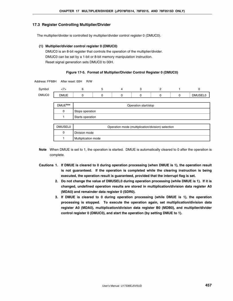
CHAPTER 17 MULTIPLIER/DIVIDER (μPD78F0514, 78F0515, AND 78F0515D ONLY)
User’s Manual U17336EJ5V0UD 457
17.3 Register Controlling Multiplier/Divider
The multiplier/divider is controlled by multiplier/divider control register 0 (DMUC0).
(1) Multiplier/divider control register 0 (DMUC0)
DMUC0 is an 8-bit register that controls the operation of the multiplier/divider.
DMUC0 can be set by a 1-bit or 8-bit memory manipulation instruction.
Reset signal generation sets DMUC0 to 00H.
Figure 17-5. Format of Multiplier/Divider Control Register 0 (DMUC0)
DMUEDMUC0 0 0 0 0 0 0 DMUSEL0
Stops operation
Starts operation
DMUENote
0
1
Operation start/stop
Division mode
Multiplication mode
DMUSEL0
0
1
Operation mode (multiplication/division) selection
Address: FF68H After reset: 00H R/W
Symbol 4 3 2 1 06<7> 5
Note When DMUE is set to 1, the operation is started. DMUE is automatically cleared to 0 after the operation is
complete.
Cautions 1. If DMUE is cleared to 0 during operation processing (when DMUE is 1), the operation result
is not guaranteed. If the operation is completed while the clearing instruction is being
executed, the operation result is guaranteed, provided that the interrupt flag is set.
2. Do not change the value of DMUSEL0 during operation processing (while DMUE is 1). If it is
changed, undefined operation results are stored in multiplication/division data register A0
(MDA0) and remainder data register 0 (SDR0).
3. If DMUE is cleared to 0 during operation processing (while DMUE is 1), the operation
processing is stopped. To execute the operation again, set multiplication/division data
register A0 (MDA0), multiplication/division data register B0 (MDB0), and multiplier/divider
control register 0 (DMUC0), and start the operation (by setting DMUE to 1).

CHAPTER 17 MULTIPLIER/DIVIDER (μPD78F0514, 78F0515, AND 78F0515D ONLY)
User’s Manual U17336EJ5V0UD 458
17.4 Operations of Multiplier/Divider
17.4.1 Multiplication operation
• Initial setting
1. Set operation data to multiplication/division data register A0L (MDA0L) and multiplication/division data register
B0 (MDB0).
2. Set bits 0 (DMUSEL0) and 7 (DMUE) of multiplier/divider control register 0 (DMUC0) to 1. Operation will start.
• During operation
3. The operation will be completed when 16 peripheral hardware clocks (fPRS) have been issued after the start of
the operation (intermediate data is stored in the MDA0L and MDA0H registers during operation, and therefore
the read values of these registers are not guaranteed).
• End of operation
4. The operation result data is stored in the MDA0L and MDA0H registers.
5. DMUE is cleared to 0 (end of operation).
6. After the operation, an interrupt request signal (INTDMU) is generated.
• Next operation
7. To execute multiplication next, start from the initial setting in 17.4.1 Multiplication operation.
8. To execute division next, start from the initial setting in 17.4.2 Division operation.
<R>
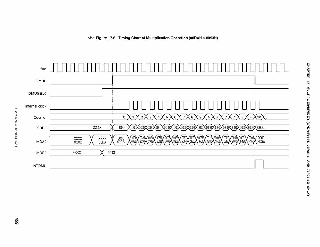
CH
AP
TE
R 17 M
UL
TIP
LIE
R/D
IVID
ER
(μPD
78F0514, 78F
0515, AN
D 78F
0515D O
NL
Y)
User’s M
anual U17336E
J5V0U
D 459
Figure 17-6. Timing Chart of Multiplication Operation (00DAH × 0093H)
fPRS
MDA0
SDR0
MDB0
1 2 3 4 5 6 7 8 9 A B C D E F 100 0
0000 0000 0000 0000 0000 0000 0000 0000 0000 0000 0000 0000 0000 0000 0000 0000 0000
0000006D
000000DA
XXXX00DA
XXXX
XXXXXXXX
00498036
0024C01B
005BE00D
00777006
003BB803
00675C01
007D2E00
003E9700
001F4B80
000FA5C0
0007D2E0
0003E970
0001F4B8
0000FA5C
00007D2E
0093XXXX
Internal clock
DMUE
DMUSEL0
Counter
INTDMU
<R>

CHAPTER 17 MULTIPLIER/DIVIDER (μPD78F0514, 78F0515, AND 78F0515D ONLY)
User’s Manual U17336EJ5V0UD 460
17.4.2 Division operation
• Initial setting
1. Set operation data to multiplication/division data register A0 (MDA0L and MDA0H) and multiplication/division
data register B0 (MDB0).
2. Set bits 0 (DMUSEL0) and 7 (DMUE) of multiplier/divider control register 0 (DMUC0) to 0 and 1, respectively.
Operation will start.
• During operation
3. The operation will be completed when 32 peripheral hardware clocks (fPRS) have been issued after the start of
the operation (intermediate data is stored in the MDA0L and MDA0H registers and remainder data register 0
(SDR0) during operation, and therefore the read values of these registers are not guaranteed).
• End of operation
4. The result data is stored in the MDA0L, MDA0H, and SDR0 registers.
5. DMUE is cleared to 0 (end of operation).
6. After the operation, an interrupt request signal (INTDMU) is generated.
• Next operation
7. To execute multiplication next, start from the initial setting in 17.4.1 Multiplication operation.
8. To execute division next, start from the initial setting in 17.4.2 Division operation.
<R>

CH
AP
TE
R 17 M
UL
TIP
LIE
R/D
IVID
ER
(μPD
78F0514, 78F
0515, AN
D 78F
0515D O
NL
Y)
User’s M
anual U17336E
J5V0U
D 461
Figure 17-7. Timing Chart of Division Operation (DCBA2586H ÷ 0018H)
fPRS
MDA0
SDR0
MDB0
1 2 3 4 5 6 7 8 19 1A 1B 1C 1D 1E 1F 200 0
0000 0001 0003 0006 000D 0003 0007 000E 0004 000B 0016 0014 0010 0008 0011 000B 0016
B9744B0C
DCBA2586
XXXX
XXXXXXXX
72E89618
E5D12C30
CBA25860
9744B0C1
2E896182
5D12C304
BA258609
0C1264D8
1824C9B0
30499361
609326C3
C1264D87
824C9B0E
0499361D
09326C3A
0018XXXX
Internal clock
DMUE
DMUSEL0
Counter
INTDMU
“0”
<R>

User’s Manual U17336EJ5V0UD 462
CHAPTER 18 INTERRUPT FUNCTIONS
18.1 Interrupt Function Types
The following two types of interrupt functions are used.
(1) Maskable interrupts
These interrupts undergo mask control. Maskable interrupts can be divided into a high interrupt priority group
and a low interrupt priority group by setting the priority specification flag registers (PR0L, PR0H, PR1L, PR1H).
Multiple interrupt servicing can be applied to low-priority interrupts when high-priority interrupts are generated. If
two or more interrupt requests, each having the same priority, are simultaneously generated, then they are
processed according to the priority of vectored interrupt servicing. For the priority order, see Table 18-1.
A standby release signal is generated and STOP and HALT modes are released.
External interrupt requests and internal interrupt requests are provided as maskable interrupts.
• 38-pin and 44-pin products External: 7, Internal: 16
• 48-pin products External: 8, Internal: 16
(2) Software interrupt
This is a vectored interrupt generated by executing the BRK instruction. It is acknowledged even when interrupts
are disabled. The software interrupt does not undergo interrupt priority control.
18.2 Interrupt Sources and Configuration
The 78K0/KC2 products have a total of 24 interrupt sources in the 38-pin and 44-pin products, 25 interrupt sources
in the 48-pin products, including maskable interrupts and software interrupts. In addition, they also have up to four
reset sources (see Table 18-1).
<R>
<R>
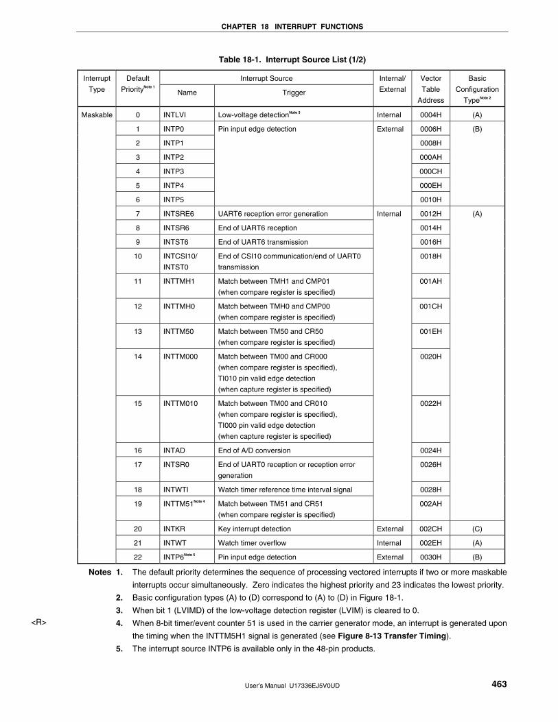
CHAPTER 18 INTERRUPT FUNCTIONS
User’s Manual U17336EJ5V0UD 463
Table 18-1. Interrupt Source List (1/2)
Interrupt Source Interrupt
Type
Default
PriorityNote 1 Name Trigger
Internal/
External
Vector
Table
Address
Basic
Configuration
TypeNote 2
0 INTLVI Low-voltage detectionNote 3 Internal 0004H (A)
1 INTP0 0006H
2 INTP1 0008H
3 INTP2 000AH
4 INTP3 000CH
5 INTP4 000EH
6 INTP5
Pin input edge detection External
0010H
(B)
7 INTSRE6 UART6 reception error generation 0012H
8 INTSR6 End of UART6 reception 0014H
9 INTST6 End of UART6 transmission 0016H
10 INTCSI10/
INTST0
End of CSI10 communication/end of UART0
transmission
0018H
11 INTTMH1 Match between TMH1 and CMP01
(when compare register is specified)
001AH
12 INTTMH0 Match between TMH0 and CMP00
(when compare register is specified)
001CH
13 INTTM50 Match between TM50 and CR50
(when compare register is specified)
001EH
14 INTTM000 Match between TM00 and CR000
(when compare register is specified),
TI010 pin valid edge detection
(when capture register is specified)
0020H
15 INTTM010 Match between TM00 and CR010
(when compare register is specified),
TI000 pin valid edge detection
(when capture register is specified)
0022H
16 INTAD End of A/D conversion 0024H
17 INTSR0 End of UART0 reception or reception error
generation
0026H
18 INTWTI Watch timer reference time interval signal 0028H
19 INTTM51Note 4 Match between TM51 and CR51
(when compare register is specified)
Internal
002AH
(A)
20 INTKR Key interrupt detection External 002CH (C)
21 INTWT Watch timer overflow Internal 002EH (A)
Maskable
22 INTP6Note 5 Pin input edge detection External 0030H (B)
Notes 1. The default priority determines the sequence of processing vectored interrupts if two or more maskable
interrupts occur simultaneously. Zero indicates the highest priority and 23 indicates the lowest priority.
2. Basic configuration types (A) to (D) correspond to (A) to (D) in Figure 18-1.
3. When bit 1 (LVIMD) of the low-voltage detection register (LVIM) is cleared to 0.
4. When 8-bit timer/event counter 51 is used in the carrier generator mode, an interrupt is generated upon
the timing when the INTTM5H1 signal is generated (see Figure 8-13 Transfer Timing).
5. The interrupt source INTP6 is available only in the 48-pin products.
<R>

CHAPTER 18 INTERRUPT FUNCTIONS
User’s Manual U17336EJ5V0UD 464
Table 18-1. Interrupt Source List (2/2)
Interrupt Source Interrupt
Type
Default
PriorityNote 1 Name Trigger
Internal/
External
Vector
Table
Address
Basic
Configuration
TypeNote 2
Maskable 23 INTIIC0/
INTDMUNote 3
End of IIC0 communication/end of
multiply/divide operation
Internal 0034H (A)
Software − BRK BRK instruction execution − 003EH (D)
RESET Reset input
POC Power-on-clear
LVI Low-voltage detectionNote 4
Reset −
WDT WDT overflow
− 0000H −
Notes 1. The default priority determines the sequence of processing vectored interrupts if two or more maskable
interrupts occur simultaneously. Zero indicates the highest priority and 23 indicates the lowest priority.
2. Basic configuration types (A) to (D) correspond to (A) to (D) in Figure 18-1.
3. The interrupt source INTDMU is available only in the μPD78F0514, 78F0515, and 78F0515D.
4. When bit 1 (LVIMD) of the low-voltage detection register (LVIM) is set to 1.
Figure 18-1. Basic Configuration of Interrupt Function (1/2)
(A) Internal maskable interrupt
Internal bus
Interrupt request
IF
MK IE PR ISP
Priority controllerVector table address generator
Standby release signal
IF: Interrupt request flag
IE: Interrupt enable flag
ISP: In-service priority flag
MK: Interrupt mask flag
PR: Priority specification flag

CHAPTER 18 INTERRUPT FUNCTIONS
User’s Manual U17336EJ5V0UD 465
Figure 18-1. Basic Configuration of Interrupt Function (2/2)
(B) External maskable interrupt (INTP0 to INTP6Note)
Internal bus
Interrupt request
IF
MK IE PR ISP
Priority controllerVector table address generator
Standby release signal
External interrupt edge enable register (EGP, EGN)
Edge detector
Note 38-pin and 44-pin products: INTP0 to INTP5
48-pin products INTP0 to INTP6
(C) External maskable interrupt (INTKR)
IF
MK IE PR ISP
Internal bus
Interrupt request Priority controller
Vector table address generator
Standby release signal
Key interrupt detector
1 when KRMn = 1 (n = 0 to 3)
(D) Software interrupt
Internal bus
Interrupt request
Priority controller Vector table address generator
IF: Interrupt request flag
IE: Interrupt enable flag
ISP: In-service priority flag
MK: Interrupt mask flag
PR: Priority specification flag
KRM: Key return mode register
<R>

CHAPTER 18 INTERRUPT FUNCTIONS
User’s Manual U17336EJ5V0UD 466
18.3 Registers Controlling Interrupt Functions
The following 6 types of registers are used to control the interrupt functions.
• Interrupt request flag register (IF0L, IF0H, IF1L, IF1H)
• Interrupt mask flag register (MK0L, MK0H, MK1L, MK1H)
• Priority specification flag register (PR0L, PR0H, PR1L, PR1H)
• External interrupt rising edge enable register (EGP)
• External interrupt falling edge enable register (EGN)
• Program status word (PSW)
Table 18-2 shows a list of interrupt request flags, interrupt mask flags, and priority specification flags corresponding
to interrupt request sources.

CHAPTER 18 INTERRUPT FUNCTIONS
User’s Manual U17336EJ5V0UD 467
Table 18-2. Flags Corresponding to Interrupt Request Sources
Interrupt Request Flag Interrupt Mask Flag Priority Specification Flag Interrupt
Source Register Register Register
INTLVI LVIIF IF0L LVIMK MK0L LVIPR PR0L
INTP0 PIF0 PMK0 PPR0
INTP1 PIF1 PMK1 PPR1
INTP2 PIF2 PMK2 PPR2
INTP3 PIF3 PMK3 PPR3
INTP4 PIF4 PMK4 PPR4
INTP5 PIF5 PMK5 PPR5
INTSRE6 SREIF6 SREMK6 SREPR6
INTSR6 SRIF6 IF0H SRMK6 MK0H SRPR6 PR0H
INTST6 STIF6 STMK6 STPR6
INTCSI10 CSIIF10
Note 1
CSIMK10
Note 2
CSIPR10
Note 3
INTST0 STIF0
Note 1
DUALIF0 Note 1
STMK0
Note 2
DUALMK0Note 2
STPR0
Note 3
DUALPR0Note 3
INTTMH1 TMIFH1 TMMKH1 TMPRH1
INTTMH0 TMIFH0 TMMKH0 TMPRH0
INTTM50 TMIF50 TMMK50 TMPR50
INTTM000 TMIF000 TMMK000 TMPR000
INTTM010 TMIF010 TMMK010 TMPR010
INTAD ADIF IF1L ADMK MK1L ADPR PR1L
INTSR0 SRIF0 SRMK0 SRPR0
INTWTI WTIIF WTIMK WTIPR
INTTM51 Note 4 TMIF51 TMMK51 TMPR51
INTKR KRIF KRMK KRPR
INTWT WTIF WTMK WTPR
INTP6Note 5 PIF6Note 5 PMK6Note 5 PPR6Note 5
INTIIC0Note 6 IICIF0Note 8 IICMK0Note 9 IICPR0Note 10
INTDMUNotes 6, 7 DMUIFNotes 7, 8
IF1H
DMUMKNotes 7, 9
MK1H
DMUPRNotes 7, 10
PR1H
Notes 1. If either interrupt source INTCSI10 or INTST0 is generated, bit 2 of IF0H is set (1).
2. Bit 2 of MK0H supports both interrupt sources INTCSI10 and INTST0.
3. Bit 2 of PR0H supports both interrupt sources INTCSI10 and INTST0.
4. When 8-bit timer/event counter 51 is used in the carrier generator mode, an interrupt is generated upon
the timing when the INTTM5H1 signal is generated (see Figure 8-13 Transfer Timing).
5. 48-pin products only.
6. Do not use serial interface IIC0 and the multiplier/divider simultaneously, because various flags
corresponding to interrupt request sources are shared among serial interface IIC0 and the
multiplier/divider. When developing software which uses serial interface IIC0, by using the CC78K0 C
compiler, do not select the “Use Multiplication and Division Code” check box on the PM+ GUI.
7. μPD78F0514, 78F0515, and 78F0515D only.
8. If either interrupt source INTIIC0 or INTDMU is generated, bit 0 of IF1H is set (1).
9. Bit 0 of MK1H supports both interrupt sources INTIIC0 and INTDMU.
10. Bit 0 of PR1H supports both interrupt sources INTIIC0 and INTDMU.
<R>
<R>
<R>
<R>
<R>
<R>
<R>

CHAPTER 18 INTERRUPT FUNCTIONS
User’s Manual U17336EJ5V0UD 468
(1) Interrupt request flag registers (IF0L, IF0H, IF1L, IF1H)
The interrupt request flags are set to 1 when the corresponding interrupt request is generated or an instruction is
executed. They are cleared to 0 when an instruction is executed upon acknowledgment of an interrupt request or
upon reset signal generation.
When an interrupt is acknowledged, the interrupt request flag is automatically cleared and then the interrupt
routine is entered.
IF0L, IF0H, IF1L, and IF1H are set by a 1-bit or 8-bit memory manipulation instruction. When IF0L and IF0H, and
IF1L and IF1H are combined to form 16-bit registers IF0 and IF1, they are set by a 16-bit memory manipulation
instruction.
Reset signal generation sets these registers to 00H.
Figure 18-2. Format of Interrupt Request Flag Registers (IF0L, IF0H, IF1L, IF1H)
Address: FFE0H After reset: 00H R/W
Symbol <7> <6> <5> <4> <3> <2> <1> <0>
IF0L SREIF6 PIF5 PIF4 PIF3 PIF2 PIF1 PIF0 LVIIF
Address: FFE1H After reset: 00H R/W
Symbol <7> <6> <5> <4> <3> <2> <1> <0>
IF0H TMIF010 TMIF000 TMIF50 TMIFH0 TMIFH1 DUALIF0
CSIIF10
STIF0
STIF6 SRIF6
Address: FFE2H After reset: 00H R/W
Symbol 7 <6> <5> <4> <3> <2> <1> <0>
IF1L 0 PIF6 Note 1 WTIF KRIF TMIF51 WTIIF SRIF0 ADIF
Address: FFE3H After reset: 00H R/W
Symbol 7 6 5 4 3 2 1 <0>
IF1H 0 0 0 0 0 0 0 IICIF0
DMUIF Note 2
XXIFX Interrupt request flag
0 No interrupt request signal is generated
1 Interrupt request is generated, interrupt request status
Notes 1. 48-pin products only.
2. μPD78F0514, 78F0515, and 78F0515D only.
Cautions 1. Be sure to clear bits 6 and 7 of IF1L to 0 in the 38-pin and 44-pin products.
Be sure to clear bit 7 of IF1L to 0 in the 48-pin products.
2. Be sure to clear bits 1 to 7 of IF1H to 0.
3. When operating a timer, serial interface, or A/D converter after standby release, operate it
once after clearing the interrupt request flag. An interrupt request flag may be set by noise.
<R>

CHAPTER 18 INTERRUPT FUNCTIONS
User’s Manual U17336EJ5V0UD 469
Caution 4. When manipulating a flag of the interrupt request flag register, use a 1-bit memory
manipulation instruction (CLR1). When describing in C language, use a bit manipulation
instruction such as “IF0L.0 = 0;” or “_asm(“clr1 IF0L, 0”);” because the compiled assembler
must be a 1-bit memory manipulation instruction (CLR1).
If a program is described in C language using an 8-bit memory manipulation instruction such
as “IF0L &= 0xfe;” and compiled, it becomes the assembler of three instructions.
mov a, IF0L
and a, #0FEH
mov IF0L, a
In this case, even if the request flag of another bit of the same interrupt request flag register
(IF0L) is set to 1 at the timing between “mov a, IF0L” and “mov IF0L, a”, the flag is cleared to
0 at “mov IF0L, a”. Therefore, care must be exercised when using an 8-bit memory
manipulation instruction in C language.
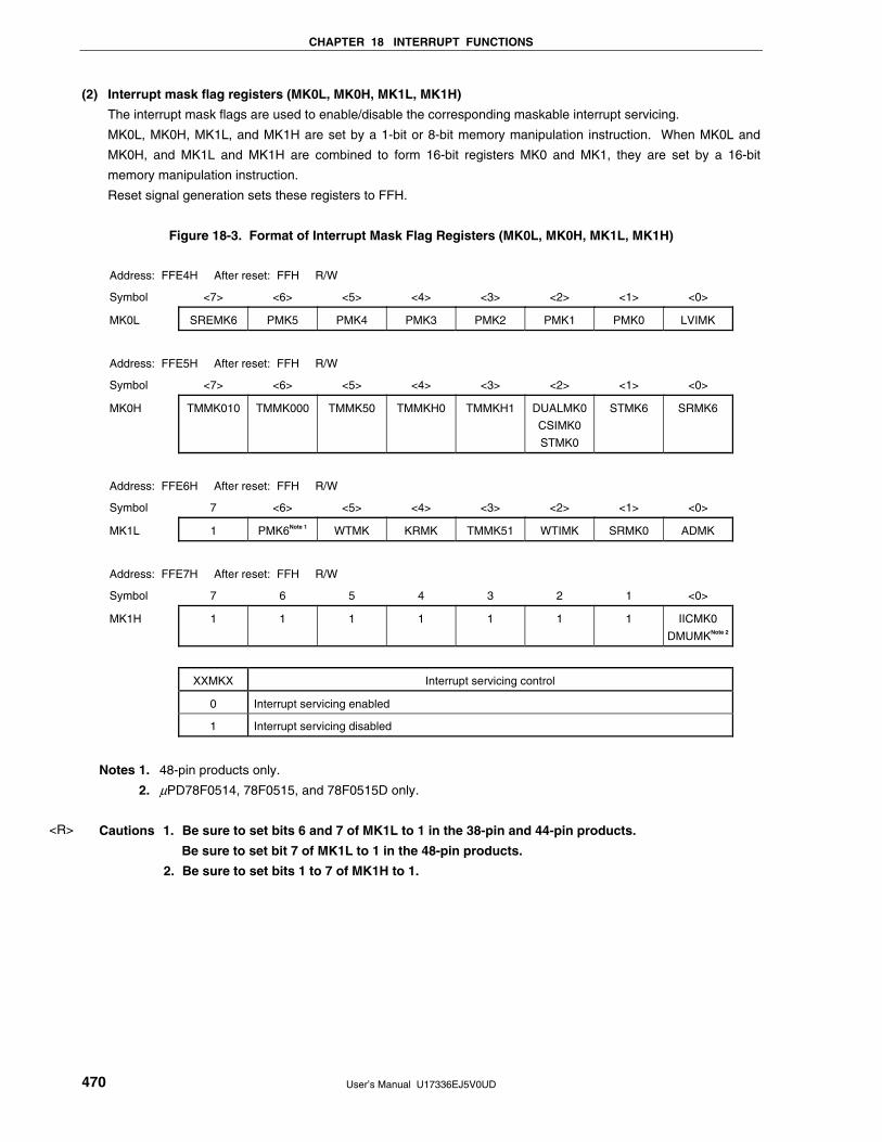
CHAPTER 18 INTERRUPT FUNCTIONS
User’s Manual U17336EJ5V0UD 470
(2) Interrupt mask flag registers (MK0L, MK0H, MK1L, MK1H)
The interrupt mask flags are used to enable/disable the corresponding maskable interrupt servicing.
MK0L, MK0H, MK1L, and MK1H are set by a 1-bit or 8-bit memory manipulation instruction. When MK0L and
MK0H, and MK1L and MK1H are combined to form 16-bit registers MK0 and MK1, they are set by a 16-bit
memory manipulation instruction.
Reset signal generation sets these registers to FFH.
Figure 18-3. Format of Interrupt Mask Flag Registers (MK0L, MK0H, MK1L, MK1H)
Address: FFE4H After reset: FFH R/W
Symbol <7> <6> <5> <4> <3> <2> <1> <0>
MK0L SREMK6 PMK5 PMK4 PMK3 PMK2 PMK1 PMK0 LVIMK
Address: FFE5H After reset: FFH R/W
Symbol <7> <6> <5> <4> <3> <2> <1> <0>
MK0H TMMK010 TMMK000 TMMK50 TMMKH0 TMMKH1 DUALMK0
CSIMK0
STMK0
STMK6 SRMK6
Address: FFE6H After reset: FFH R/W
Symbol 7 <6> <5> <4> <3> <2> <1> <0>
MK1L 1 PMK6Note 1 WTMK KRMK TMMK51 WTIMK SRMK0 ADMK
Address: FFE7H After reset: FFH R/W
Symbol 7 6 5 4 3 2 1 <0>
MK1H 1 1 1 1 1 1 1 IICMK0
DMUMKNote 2
XXMKX Interrupt servicing control
0 Interrupt servicing enabled
1 Interrupt servicing disabled
Notes 1. 48-pin products only.
2. μPD78F0514, 78F0515, and 78F0515D only.
Cautions 1. Be sure to set bits 6 and 7 of MK1L to 1 in the 38-pin and 44-pin products.
Be sure to set bit 7 of MK1L to 1 in the 48-pin products.
2. Be sure to set bits 1 to 7 of MK1H to 1.
<R>

CHAPTER 18 INTERRUPT FUNCTIONS
User’s Manual U17336EJ5V0UD 471
(3) Priority specification flag registers (PR0L, PR0H, PR1L, PR1H)
The priority specification flag registers are used to set the corresponding maskable interrupt priority order.
PR0L, PR0H, PR1L, and PR1H are set by a 1-bit or 8-bit memory manipulation instruction. If PR0L and PR0H,
and PR1L and PR1H are combined to form 16-bit registers PR0 and PR1, they are set by a 16-bit memory
manipulation instruction.
Reset signal generation sets these registers to FFH.
Figure 18-4. Format of Priority Specification Flag Registers (PR0L, PR0H, PR1L, PR1H)
Address: FFE8H After reset: FFH R/W
Symbol <7> <6> <5> <4> <3> <2> <1> <0>
PR0L SREPR6 PPR5 PPR4 PPR3 PPR2 PPR1 PPR0 LVIPR
Address: FFE9H After reset: FFH R/W
Symbol <7> <6> <5> <4> <3> <2> <1> <0>
PR0H TMPR010 TMPR000 TMPR50 TMPRH0 TMPRH1 DUALPR0
CSIPR10
STPR0
STPR6 SRPR6
Address: FFEAH After reset: FFH R/W
Symbol 7 <6> <5> <4> <3> <2> <1> <0>
PR1L 1 PPR6Note 1 WTPR KRPR TMPR51 WTIPR SRPR0 ADPR
Address: FFEBH After reset: FFH R/W
Symbol 7 6 5 4 3 2 1 <0>
PR1H 1 1 1 1 1 1 1 IICPR0
DMUPRNote 2
XXPRX Priority level selection
0 High priority level
1 Low priority level
Notes 1. 48-pin products only.
2. μPD78F0514, 78F0515, and 78F0515D only.
Cautions 1. Be sure to set bits 6 and 7 of PR1L to 1 in the 38-pin and 44-pin products.
Be sure to set bit 7 of PR1L to 1 in the 48-pin products.
2. Be sure to set bits 1 to 7 of PR1H to 1.
<R>

CHAPTER 18 INTERRUPT FUNCTIONS
User’s Manual U17336EJ5V0UD 472
(4) External interrupt rising edge enable register (EGP), external interrupt falling edge enable register (EGN)
These registers specify the valid edge for INTP0 to INTP6.
EGP and EGN are set by a 1-bit or 8-bit memory manipulation instruction.
Reset signal generation sets these registers to 00H.
Figure 18-5. Format of External Interrupt Rising Edge Enable Register (EGP)
and External Interrupt Falling Edge Enable Register (EGN)
Address: FF48H After reset: 00H R/W
Symbol 7 6 5 4 3 2 1 0
EGP 0 EGP6Note EGP5 EGP4 EGP3 EGP2 EGP1 EGP0
Address: FF49H After reset: 00H R/W
Symbol 7 6 5 4 3 2 1 0
EGN 0 EGN6Note EGN5 EGN4 EGN3 EGN2 EGN1 EGN0
EGPn EGNn INTPn pin valid edge selection (n = 0 to 6)
0 0 Edge detection disabled
0 1 Falling edge
1 0 Rising edge
1 1 Both rising and falling edges
Note 48-pin products only.
Caution Be sure to clear bits 6 and 7 of EGP and EGN to 0 in the 38-pin and 44-pin products.
Be sure to clear bit 7 of EGP and EGN to 0 in the 48-pin products.
Table 18-3 shows the ports corresponding to EGPn and EGNn.
Table 18-3. Ports Corresponding to EGPn and EGNn
Detection Enable Register Edge Detection Port Interrupt Request Signal
EGP0 EGN0 P120 INTP0
EGP1 EGN1 P30 INTP1
EGP2 EGN2 P31 INTP2
EGP3 EGN3 P32 INTP3
EGP4 EGN4 P33 INTP4
EGP5 EGN5 P16 INTP5
EGP6Note EGN6Note P140Note INTP6Note
Note 48-pin products only.
Caution Select the port mode by clearing EGPn and EGNn to 0 because an edge may be
detected when the external interrupt function is switched to the port function.
Remark 38-pin and 44-pin products: n = 0 to 5
48-pin products: n = 0 to 6
<R>

CHAPTER 18 INTERRUPT FUNCTIONS
User’s Manual U17336EJ5V0UD 473
(5) Program status word (PSW)
The program status word is a register used to hold the instruction execution result and the current status for an
interrupt request. The IE flag that sets maskable interrupt enable/disable and the ISP flag that controls multiple
interrupt servicing are mapped to the PSW.
Besides 8-bit read/write, this register can carry out operations using bit manipulation instructions and dedicated
instructions (EI and DI). When a vectored interrupt request is acknowledged, if the BRK instruction is executed,
the contents of the PSW are automatically saved into a stack and the IE flag is reset to 0. If a maskable interrupt
request is acknowledged, the contents of the priority specification flag of the acknowledged interrupt are
transferred to the ISP flag. The PSW contents are also saved into the stack with the PUSH PSW instruction.
They are restored from the stack with the RETI, RETB, and POP PSW instructions.
Reset signal generation sets PSW to 02H.
Figure 18-6. Format of Program Status Word
<7>
IE
<6>
Z
<5>
RBS1
<4>
AC
<3>
RBS0
2
0
<1>
ISP
0
CYPSW
After reset
02H
ISP
High-priority interrupt servicing (low-priority interrupt disabled)
IE
0
1
Disabled
Priority of interrupt currently being serviced
Interrupt request acknowledgment enable/disable
Used when normal instruction is executed
Enabled
Interrupt request not acknowledged, or low-priority interrupt servicing (all maskable interrupts enabled)
0
1

CHAPTER 18 INTERRUPT FUNCTIONS
User’s Manual U17336EJ5V0UD 474
18.4 Interrupt Servicing Operations
18.4.1 Maskable interrupt acknowledgment
A maskable interrupt becomes acknowledgeable when the interrupt request flag is set to 1 and the mask (MK) flag
corresponding to that interrupt request is cleared to 0. A vectored interrupt request is acknowledged if interrupts are
in the interrupt enabled state (when the IE flag is set to 1). However, a low-priority interrupt request is not
acknowledged during servicing of a higher priority interrupt request (when the ISP flag is reset to 0).
The times from generation of a maskable interrupt request until vectored interrupt servicing is performed are listed
in Table 18-4 below.
For the interrupt request acknowledgment timing, see Figures 18-8 and 18-9.
Table 18-4. Time from Generation of Maskable Interrupt Until Servicing
Minimum Time Maximum TimeNote
When ××PR = 0 7 clocks 32 clocks
When ××PR = 1 8 clocks 33 clocks
Note If an interrupt request is generated just before a divide instruction, the wait time becomes longer.
Remark 1 clock: 1/fCPU (fCPU: CPU clock)
If two or more maskable interrupt requests are generated simultaneously, the request with a higher priority level
specified in the priority specification flag is acknowledged first. If two or more interrupts requests have the same
priority level, the request with the highest default priority is acknowledged first.
An interrupt request that is held pending is acknowledged when it becomes acknowledgeable.
Figure 18-7 shows the interrupt request acknowledgment algorithm.
If a maskable interrupt request is acknowledged, the contents are saved into the stacks in the order of PSW, then
PC, the IE flag is reset (0), and the contents of the priority specification flag corresponding to the acknowledged
interrupt are transferred to the ISP flag. The vector table data determined for each interrupt request is the loaded into
the PC and branched.
Restoring from an interrupt is possible by using the RETI instruction.
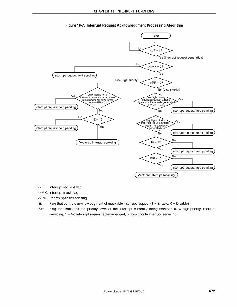
CHAPTER 18 INTERRUPT FUNCTIONS
User’s Manual U17336EJ5V0UD 475
Figure 18-7. Interrupt Request Acknowledgment Processing Algorithm
Start
××IF = 1?
××MK = 0?
××PR = 0?
IE = 1?
ISP = 1?
Interrupt request held pending
Yes
Yes
No
No
Yes (interrupt request generation)
Yes
No (Low priority)
No
No
Yes
Yes
No
IE = 1?
No
Any high-priority interrupt request among those
simultaneously generated with ××PR = 0?
Yes (High priority)
No
Yes
Yes
No
Vectored interrupt servicing
Interrupt request held pending
Interrupt request held pending
Interrupt request held pending
Interrupt request held pending
Interrupt request held pending
Interrupt request held pending
Vectored interrupt servicing
Any high-priority interrupt request among
those simultaneously generated?
Any high-priority interrupt request among
those simultaneously generated with ××PR = 0?
××IF: Interrupt request flag
××MK: Interrupt mask flag
××PR: Priority specification flag
IE: Flag that controls acknowledgment of maskable interrupt request (1 = Enable, 0 = Disable)
ISP: Flag that indicates the priority level of the interrupt currently being serviced (0 = high-priority interrupt
servicing, 1 = No interrupt request acknowledged, or low-priority interrupt servicing)

CHAPTER 18 INTERRUPT FUNCTIONS
User’s Manual U17336EJ5V0UD 476
Figure 18-8. Interrupt Request Acknowledgment Timing (Minimum Time)
8 clocks
7 clocks
Instruction InstructionPSW and PC saved, jump to interrupt servicing
Interrupt servicing program
CPU processing
××IF(××PR = 1)
××IF(××PR = 0)
6 clocks
Remark 1 clock: 1/fCPU (fCPU: CPU clock)
Figure 18-9. Interrupt Request Acknowledgment Timing (Maximum Time)
33 clocks
32 clocks
Instruction Divide instructionPSW and PC saved, jump to interrupt servicing
Interrupt servicing program
CPU processing
××IF(××PR = 1)
××IF(××PR = 0)
6 clocks25 clocks
Remark 1 clock: 1/fCPU (fCPU: CPU clock)
18.4.2 Software interrupt request acknowledgment
A software interrupt request is acknowledged by BRK instruction execution. Software interrupts cannot be disabled.
If a software interrupt request is acknowledged, the contents are saved into the stacks in the order of the program
status word (PSW), then program counter (PC), the IE flag is reset (0), and the contents of the vector table (003EH,
003FH) are loaded into the PC and branched.
Restoring from a software interrupt is possible by using the RETB instruction.
Caution Do not use the RETI instruction for restoring from the software interrupt.

CHAPTER 18 INTERRUPT FUNCTIONS
User’s Manual U17336EJ5V0UD 477
18.4.3 Multiple interrupt servicing
Multiple interrupt servicing occurs when another interrupt request is acknowledged during execution of an interrupt.
Multiple interrupt servicing does not occur unless the interrupt request acknowledgment enabled state is selected
(IE = 1). When an interrupt request is acknowledged, interrupt request acknowledgment becomes disabled (IE = 0).
Therefore, to enable multiple interrupt servicing, it is necessary to set (1) the IE flag with the EI instruction during
interrupt servicing to enable interrupt acknowledgment.
Moreover, even if interrupts are enabled, multiple interrupt servicing may not be enabled, this being subject to
interrupt priority control. Two types of priority control are available: default priority control and programmable priority
control. Programmable priority control is used for multiple interrupt servicing.
In the interrupt enabled state, if an interrupt request with a priority equal to or higher than that of the interrupt
currently being serviced is generated, it is acknowledged for multiple interrupt servicing. If an interrupt with a priority
lower than that of the interrupt currently being serviced is generated during interrupt servicing, it is not acknowledged
for multiple interrupt servicing. Interrupt requests that are not enabled because interrupts are in the interrupt disabled
state or because they have a lower priority are held pending. When servicing of the current interrupt ends, the
pending interrupt request is acknowledged following execution of at least one main processing instruction execution.
Table 18-5 shows relationship between interrupt requests enabled for multiple interrupt servicing and Figure 18-10
shows multiple interrupt servicing examples.
Table 18-5. Relationship Between Interrupt Requests Enabled for Multiple Interrupt Servicing
During Interrupt Servicing
Maskable Interrupt Request
PR = 0 PR = 1
Multiple Interrupt Request
Interrupt Being Serviced IE = 1 IE = 0 IE = 1 IE = 0
Software
Interrupt
Request
ISP = 0 × × × Maskable interrupt
ISP = 1 × ×
Software interrupt × ×
Remarks 1. : Multiple interrupt servicing enabled
2. ×: Multiple interrupt servicing disabled
3. ISP and IE are flags contained in the PSW.
ISP = 0: An interrupt with higher priority is being serviced.
ISP = 1: No interrupt request has been acknowledged, or an interrupt with a lower
priority is being serviced.
IE = 0: Interrupt request acknowledgment is disabled.
IE = 1: Interrupt request acknowledgment is enabled.
4. PR is a flag contained in PR0L, PR0H, PR1L, and PR1H.
PR = 0: Higher priority level
PR = 1: Lower priority level

CHAPTER 18 INTERRUPT FUNCTIONS
User’s Manual U17336EJ5V0UD 478
Figure 18-10. Examples of Multiple Interrupt Servicing (1/2)
Example 1. Multiple interrupt servicing occurs twice
Main processing INTxx servicing INTyy servicing INTzz servicing
EIEI EI
RETI RETI
RETI
INTxx(PR = 1)
INTyy(PR = 0)
INTzz(PR = 0)
IE = 0 IE = 0 IE = 0
IE = 1 IE = 1IE = 1
During servicing of interrupt INTxx, two interrupt requests, INTyy and INTzz, are acknowledged, and multiple
interrupt servicing takes place. Before each interrupt request is acknowledged, the EI instruction must always be
issued to enable interrupt request acknowledgment.
Example 2. Multiple interrupt servicing does not occur due to priority control
Main processing INTxx servicing INTyy servicing
INTxx(PR = 0)
INTyy(PR = 1)
EI
RETI
IE = 0
IE = 0EI
1 instruction execution
RETIIE = 1
IE = 1
Interrupt request INTyy issued during servicing of interrupt INTxx is not acknowledged because its priority is lower
than that of INTxx, and multiple interrupt servicing does not take place. The INTyy interrupt request is held pending,
and is acknowledged following execution of one main processing instruction.
PR = 0: Higher priority level
PR = 1: Lower priority level
IE = 0: Interrupt request acknowledgment disabled

CHAPTER 18 INTERRUPT FUNCTIONS
User’s Manual U17336EJ5V0UD 479
Figure 18-10. Examples of Multiple Interrupt Servicing (2/2)
Example 3. Multiple interrupt servicing does not occur because interrupts are not enabled
Main processing INTxx servicing INTyy servicing
EI
1 instruction execution
RETI
RETI
INTxx(PR = 0)
INTyy(PR = 0)
IE = 0
IE = 0
IE = 1
IE = 1
Interrupts are not enabled during servicing of interrupt INTxx (EI instruction is not issued), therefore, interrupt
request INTyy is not acknowledged and multiple interrupt servicing does not take place. The INTyy interrupt request
is held pending, and is acknowledged following execution of one main processing instruction.
PR = 0: Higher priority level
IE = 0: Interrupt request acknowledgment disabled

CHAPTER 18 INTERRUPT FUNCTIONS
User’s Manual U17336EJ5V0UD 480
18.4.4 Interrupt request hold
There are instructions where, even if an interrupt request is issued for them while another instruction is being
executed, request acknowledgment is held pending until the end of execution of the next instruction. These
instructions (interrupt request hold instructions) are listed below.
• MOV PSW, #byte
• MOV A, PSW
• MOV PSW, A
• MOV1 PSW. bit, CY
• MOV1 CY, PSW. bit
• AND1 CY, PSW. bit
• OR1 CY, PSW. bit
• XOR1 CY, PSW. bit
• SET1 PSW. bit
• CLR1 PSW. bit
• RETB
• RETI
• PUSH PSW
• POP PSW
• BT PSW. bit, $addr16
• BF PSW. bit, $addr16
• BTCLR PSW. bit, $addr16
• EI
• DI
• Manipulation instructions for the IF0L, IF0H, IF1L, IF1H, MK0L, MK0H, MK1L, MK1H, PR0L, PR0H, PR1L, and
PR1H registers.
Caution The BRK instruction is not one of the above-listed interrupt request hold instructions. However,
the software interrupt activated by executing the BRK instruction causes the IE flag to be cleared.
Therefore, even if a maskable interrupt request is generated during execution of the BRK
instruction, the interrupt request is not acknowledged.
Figure 18-11 shows the timing at which interrupt requests are held pending.
Figure 18-11. Interrupt Request Hold
Instruction N Instruction MPSW and PC saved, jump to interrupt servicing
Interrupt servicingprogram
CPU processing
××IF
Remarks 1. Instruction N: Interrupt request hold instruction
2. Instruction M: Instruction other than interrupt request hold instruction
3. The ××PR (priority level) values do not affect the operation of ××IF (interrupt request).

User’s Manual U17336EJ5V0UD 481
CHAPTER 19 KEY INTERRUPT FUNCTION
19.1 Functions of Key Interrupt
A key interrupt (INTKR) can be generated by setting the key return mode register (KRM) and inputting a falling
edge to the key interrupt input pins (KR0 to KR3Note).
Note 38-pin products: KR0, KR1
44-pin and 48-pin products: KR0 to KR3
Table 19-1. Assignment of Key Interrupt Detection Pins
Flag Description
KRM0 Controls KR0 signal in 1-bit units.
KRM1 Controls KR1 signal in 1-bit units.
KRM2 Controls KR2 signal in 1-bit units.
KRM3 Controls KR3 signal in 1-bit units.
19.2 Configuration of Key Interrupt
The key interrupt includes the following hardware.
Table 19-2. Configuration of Key Interrupt
Item Configuration
Control register Key return mode register (KRM)
Figure 19-1. Block Diagram of Key Interrupt
INTKR
Key return mode register (KRM)
0 0 0 0 KRM3 KRM2 KRM1 KRM0
KR3Note
KR2Note
KR1
KR0
Note 44-pin and 48-pin products only
<R>
<R>

CHAPTER 19 KEY INTERRUPT FUNCTION
User’s Manual U17336EJ5V0UD 482
19.3 Register Controlling Key Interrupt
(1) Key return mode register (KRM)
This register controls the KRM0 to KRM3 bits using the KR0 to KR3 signals, respectively.
KRM is set by a 1-bit or 8-bit memory manipulation instruction.
Reset signal generation sets KRM to 00H.
Figure 19-2. Format of Key Return Mode Register (KRM)
0
Does not detect key interrupt signal
Detects key interrupt signal
KRMn
0
1
Key interrupt mode control
KRM 0 0 0 KRM3 KRM2 KRM1 KRM0
Address: FF6EH After reset: 00H R/W
Symbol 7 6 5 4 3 2 0
Cautions 1. For the 38-pin products, be sure to set bits 2 and 3 of KRM, PM7, and P7 to “0”.
2. If any of the KRM0 to KRM3 bits used is set to 1, set bits 0 to 3 (PU70 to PU73) of the
corresponding pull-up resistor register 7 (PU7) to 1.
3. If KRM is changed, the interrupt request flag may be set. Therefore, disable interrupts and
then change the KRM register. Clear the interrupt request flag and enable interrupts.
4. The bits not used in the key interrupt mode can be used as normal ports.
<R>

User’s Manual U17336EJ5V0UD 483
CHAPTER 20 STANDBY FUNCTION
20.1 Standby Function and Configuration
20.1.1 Standby function
The standby function is designed to reduce the operating current of the system. The following two modes are
available.
(1) HALT mode
HALT instruction execution sets the HALT mode. In the HALT mode, the CPU operation clock is stopped. If the
high-speed system clock oscillator, internal high-speed oscillator, internal low-speed oscillator, or subsystem
clock oscillator is operating before the HALT mode is set, oscillation of each clock continues. In this mode, the
operating current is not decreased as much as in the STOP mode, but the HALT mode is effective for restarting
operation immediately upon interrupt request generation and carrying out intermittent operations frequently.
(2) STOP mode
STOP instruction execution sets the STOP mode. In the STOP mode, the high-speed system clock oscillator and
internal high-speed oscillator stop, stopping the whole system, thereby considerably reducing the CPU operating
current.
Because this mode can be cleared by an interrupt request, it enables intermittent operations to be carried out.
However, because a wait time is required to secure the oscillation stabilization time after the STOP mode is
released when the X1 clock is selected, select the HALT mode if it is necessary to start processing immediately
upon interrupt request generation.
In either of these two modes, all the contents of registers, flags and data memory just before the standby mode is
set are held. The I/O port output latches and output buffer statuses are also held.
Cautions 1. The STOP mode can be used only when the CPU is operating on the main system clock. The
subsystem clock oscillation cannot be stopped. The HALT mode can be used when the CPU
is operating on either the main system clock or the subsystem clock.
2. When shifting to the STOP mode, be sure to stop the peripheral hardware operation
operating with main system clock before executing STOP instruction.
3. The following sequence is recommended for operating current reduction of the A/D converter
when the standby function is used: First clear bit 7 (ADCS) and bit 0 (ADCE) of the A/D
converter mode register (ADM) to 0 to stop the A/D conversion operation, and then execute
the STOP instruction.
20.1.2 Registers controlling standby function
The standby function is controlled by the following two registers.
• Oscillation stabilization time counter status register (OSTC)
• Oscillation stabilization time select register (OSTS)
Remark For the registers that start, stop, or select the clock, see CHAPTER 5 CLOCK GENERATOR.

CHAPTER 20 STANDBY FUNCTION
User’s Manual U17336EJ5V0UD 484
(1) Oscillation stabilization time counter status register (OSTC)
This is the register that indicates the count status of the X1 clock oscillation stabilization time counter. When X1
clock oscillation starts with the internal high-speed oscillation clock or subsystem clock used as the CPU clock,
the X1 clock oscillation stabilization time can be checked.
OSTC can be read by a 1-bit or 8-bit memory manipulation instruction.
When reset is released (reset by RESET input, POC, LVI, and WDT), the STOP instruction and MSTOP (bit 7 of
MOC register) = 1 clear OSTC to 00H.
Figure 20-1. Format of Oscillation Stabilization Time Counter Status Register (OSTC)
Address: FFA3H After reset: 00H R
Symbol 7 6 5 4 3 2 1 0
OSTC 0 0 0 MOST11 MOST13 MOST14 MOST15 MOST16
MOST11 MOST13 MOST14 MOST15 MOST16 Oscillation stabilization time status
fX = 10 MHz fX = 20 MHz
1 0 0 0 0 211/fX min. 204.8 μs min. 102.4 μs min.
1 1 0 0 0 213/fX min. 819.2 μs min. 409.6 μs min.
1 1 1 0 0 214/fX min. 1.64 ms min. 819.2 μs min.
1 1 1 1 0 215/fX min. 3.27 ms min. 1.64 ms min.
1 1 1 1 1 216/fX min. 6.55 ms min. 3.27 ms min.
Cautions 1. After the above time has elapsed, the bits are set to 1 in order from MOST11 and
remain 1.
2. The oscillation stabilization time counter counts up to the oscillation
stabilization time set by OSTS. If the STOP mode is entered and then released
while the internal high-speed oscillation clock is being used as the CPU clock,
set the oscillation stabilization time as follows.
• Desired OSTC oscillation stabilization time ≤ Oscillation stabilization time
set by OSTS
Note, therefore, that only the status up to the oscillation stabilization time set by
OSTS is set to OSTC after STOP mode is released.
3. The X1 clock oscillation stabilization wait time does not include the time until
clock oscillation starts (“a” below).
STOP mode release
X1 pin voltage waveform
a
Remark fX: X1 clock oscillation frequency

CHAPTER 20 STANDBY FUNCTION
User’s Manual U17336EJ5V0UD 485
(2) Oscillation stabilization time select register (OSTS)
This register is used to select the X1 clock oscillation stabilization wait time when the STOP mode is released.
When the X1 clock is selected as the CPU clock, the operation waits for the time set using OSTS after the STOP
mode is released.
When the internal high-speed oscillation clock is selected as the CPU clock, confirm with OSTC that the desired
oscillation stabilization time has elapsed after the STOP mode is released. The oscillation stabilization time can
be checked up to the time set using OSTC.
OSTS can be set by an 8-bit memory manipulation instruction.
Reset signal generation sets OSTS to 05H.
Figure 20-2. Format of Oscillation Stabilization Time Select Register (OSTS)
Address: FFA4H After reset: 05H R/W
Symbol 7 6 5 4 3 2 1 0
OSTS 0 0 0 0 0 OSTS2 OSTS1 OSTS0
OSTS2 OSTS1 OSTS0 Oscillation stabilization time selection
fX = 10 MHz fX = 20 MHz
0 0 1 211/fX 204.8 μs 102.4 μs
0 1 0 213/fX 819.2 μs 409.6 μs
0 1 1 214/fX 1.64 ms 819.2 μs
1 0 0 215/fX 3.27 ms 1.64 ms
1 0 1 216/fX 6.55 ms 3.27 ms
Other than above Setting prohibited
Cautions 1. To set the STOP mode when the X1 clock is used as the CPU clock, set OSTS
before executing the STOP instruction.
2. Do not change the value of the OSTS register during the X1 clock oscillation
stabilization time.
3. The oscillation stabilization time counter counts up to the oscillation
stabilization time set by OSTS. If the STOP mode is entered and then released
while the internal high-speed oscillation clock is being used as the CPU clock,
set the oscillation stabilization time as follows.
• Desired OSTC oscillation stabilization time ≤ Oscillation stabilization time
set by OSTS
Note, therefore, that only the status up to the oscillation stabilization time set by
OSTS is set to OSTC after STOP mode is released.
4. The X1 clock oscillation stabilization wait time does not include the time until
clock oscillation starts (“a” below).
STOP mode release
X1 pin voltage waveform
a
Remark fX: X1 clock oscillation frequency
CHAPTER 20 STANDBY FUNCTION
User’s Manual U17336EJ5V0UD 486
20.2 Standby Function Operation
20.2.1 HALT mode
(1) HALT mode
The HALT mode is set by executing the HALT instruction. HALT mode can be set regardless of whether the CPU
clock before the setting was the high-speed system clock, internal high-speed oscillation clock, or subsystem
clock.
The operating statuses in the HALT mode are shown below.

CHAPTER 20 STANDBY FUNCTION
User’s Manual U17336EJ5V0UD 487
Table 20-1. Operating Statuses in HALT Mode (1/2)
When HALT Instruction Is Executed While CPU Is Operating on Main System Clock HALT Mode Setting
Item
When CPU Is Operating on Internal High-Speed
Oscillation Clock (fRH)
When CPU Is Operating on X1 Clock (fX)
When CPU Is Operating on External Main System Clock
(fEXCLK)
System clock Clock supply to the CPU is stopped
fRH Operation continues (cannot be stopped)
Status before HALT mode was set is continued
fX Status before HALT mode was set is continued
Operation continues (cannot be stopped)
Status before HALT mode was set is retained
Main system clock
fEXCLK Operates or stops by external clock input Operation continues (cannot be stopped)
fXT Status before HALT mode was set is continued
Subsystem clock
fEXCLKS Operates or stops by external clock input
fRL Status before HALT mode was set is continued
CPU
Flash memory
Operation stopped
RAM
Port (latch)
Status before HALT mode was set is retained
16-bit timer/event counter 00
50 8-bit timer/event counter 51
H0 8-bit timer
H1
Watch timer
Operable
Watchdog timer Operable. Clock supply to watchdog timer stops when “internal low-speed oscillator can be stopped by software” is set by option byte.
Clock outputNote 1
A/D converter
UART0
UART6
CSI10
Serial interface
IIC0
Multiplier/dividerNote 2
Power-on-clear function
Low-voltage detection function
External interrupt
Operable
Notes 1. 48-pin products only.
2. μPD78F0514, 78F0515, and 78F0515D only.
Remark fRH: Internal high-speed oscillation clock
fX: X1 clock
fEXCLK: External main system clock
fXT: XT1 clock
fEXCLKS: External subsystem clock
fRL: Internal low-speed oscillation clock

CHAPTER 20 STANDBY FUNCTION
User’s Manual U17336EJ5V0UD 488
Table 20-1. Operating Statuses in HALT Mode (2/2)
When HALT Instruction Is Executed While CPU Is Operating on Subsystem Clock HALT Mode Setting
Item
When CPU Is Operating on XT1 Clock (fXT) When CPU Is Operating on External
Subsystem Clock (fEXCLKS)
System clock Clock supply to the CPU is stopped
fRH
fX
Status before HALT mode was set is continued
Main system clock
fEXCLK Operates or stops by external clock input
fXT Operation continues (cannot be stopped) Status before HALT mode was set is continued
Subsystem clock
fEXCLKS Operates or stops by external clock input Operation continues (cannot be stopped)
fRL Status before HALT mode was set is continued
CPU
Flash memory
Operation stopped
RAM
Port (latch)
Status before HALT mode was set is retained
16-bit timer/event counter 00Note 1
50Note 1 8-bit timer/event
counter 51Note 1
H0 8-bit timer
H1
Watch timer
Operable
Watchdog timer Operable. Clock supply to watchdog timer stops when “internal low-speed oscillator can be
stopped by software” is set by option byte.
Clock outputNote 2 Operable
A/D converter Operable. However, operation disabled when peripheral hardware clock (fPRS) is stopped.
UART0
UART6
CSI10Note 1
Serial interface
IIC0Note 1
Multiplier/dividerNote 3
Power-on-clear function
Low-voltage detection function
External interrupt
Operable
Notes 1. When the CPU is operating on the subsystem clock and the internal high-speed oscillation clock has been
stopped, do not start operation of these functions on the external clock input from peripheral hardware pins.
2. 48-pin products only.
3. μPD78F0514, 78F0515, and 78F0515D only.
Remark fRH: Internal high-speed oscillation clock
fX: X1 clock
fEXCLK: External main system clock
fXT: XT1 clock
fEXCLKS: External subsystem clock
fRL: Internal low-speed oscillation clock

CHAPTER 20 STANDBY FUNCTION
User’s Manual U17336EJ5V0UD 489
(2) HALT mode release
The HALT mode can be released by the following two sources.
(a) Release by unmasked interrupt request
When an unmasked interrupt request is generated, the HALT mode is released. If interrupt acknowledgment
is enabled, vectored interrupt servicing is carried out. If interrupt acknowledgment is disabled, the next
address instruction is executed.
Figure 20-3. HALT Mode Release by Interrupt Request Generation
HALTinstruction
WaitNote Normal operationHALT modeNormal operation
OscillationHigh-speed system clock,internal high-speed oscillation clock,
or subsystem clock
Status of CPU
Standbyrelease signal
Interruptrequest
Note The wait time is as follows:
• When vectored interrupt servicing is carried out: 8 or 9 clocks
• When vectored interrupt servicing is not carried out: 2 or 3 clocks
Remark The broken line indicates the case when the interrupt request which has released the standby
mode is acknowledged.

CHAPTER 20 STANDBY FUNCTION
User’s Manual U17336EJ5V0UD 490
(b) Release by reset signal generation
When the reset signal is generated, HALT mode is released, and then, as in the case with a normal reset
operation, the program is executed after branching to the reset vector address.
Figure 20-4. HALT Mode Release by Reset
(1) When high-speed system clock is used as CPU clock
HALT
instruction
Reset signal
High-speedsystem clock
(X1 oscillation)
HALT modeResetperiod
OscillatesOscillationstopped Oscillates
Status of CPU
Normal operation(high-speed
system clock)
Oscillation stabilization time(211/fX to 216/fX)
Normal operation(internal high-speed
oscillation clock)
Oscillationstopped
Starting X1 oscillation is specified by software.
Resetprocessing(11 to 45 s)μ
(2) When internal high-speed oscillation clock is used as CPU clock
HALT
instruction
Reset signal
Internal high-speedoscillation clock
Normal operation(internal high-speed
oscillation clock) HALT modeResetperiod
Normal operation(internal high-speed
oscillation clock)
OscillatesOscillationstopped Oscillates
Status of CPU
Wait for oscillationaccuracy stabilization
(86 to 361 s)
Resetprocessing(11 to 45 s)μ
μ
(3) When subsystem clock is used as CPU clock
HALT
instruction
Reset signal
Subsystem clock(XT1 oscillation)
Normal operation(subsystem clock) HALT mode
Resetperiod
Normal operation mode(internal high-speed
oscillation clock)
OscillatesOscillationstopped Oscillates
Status of CPU
Oscillationstopped
Starting XT1 oscillation is specified by software.
Resetprocessing(11 to 45 s)μ
Remark fX: X1 clock oscillation frequency

CHAPTER 20 STANDBY FUNCTION
User’s Manual U17336EJ5V0UD 491
Table 20-2. Operation in Response to Interrupt Request in HALT Mode
Release Source MK×× PR×× IE ISP Operation
0 0 0 × Next address
instruction execution
0 0 1 × Interrupt servicing
execution
0 1 0 1
0 1 × 0
Next address
instruction execution
0 1 1 1 Interrupt servicing
execution
Maskable interrupt
request
1 × × × HALT mode held
Reset − − × × Reset processing
×: don’t care
20.2.2 STOP mode
(1) STOP mode setting and operating statuses
The STOP mode is set by executing the STOP instruction, and it can be set only when the CPU clock before the
setting was the main system clock.
Caution Because the interrupt request signal is used to clear the standby mode, if there is an interrupt
source with the interrupt request flag set and the interrupt mask flag reset, the standby mode is
immediately cleared if set. Thus, the STOP mode is reset to the HALT mode immediately after
execution of the STOP instruction and the system returns to the operating mode as soon as the
wait time set using the oscillation stabilization time select register (OSTS) has elapsed.
The operating statuses in the STOP mode are shown below.

CHAPTER 20 STANDBY FUNCTION
User’s Manual U17336EJ5V0UD 492
Table 20-3. Operating Statuses in STOP Mode
When STOP Instruction Is Executed While CPU Is Operating on Main System Clock STOP Mode Setting
Item
When CPU Is Operating on Internal High-Speed
Oscillation Clock (fRH)
When CPU Is Operating on X1 Clock (fX)
When CPU Is Operating on External Main System Clock
(fEXCLK)
System clock Clock supply to the CPU is stopped
fRH
fX
Stopped
Main system clock
fEXCLK Input invalid
fXT Status before STOP mode was set is continued
Subsystem clock
fEXCLKS Operates or stops by external clock input
fRL Status before STOP mode was set is continued
CPU
Flash memory
Operation stopped
RAM
Port (latch)
Status before STOP mode was set is retained
16-bit timer/event counter 00Note 1 Operation stopped
50Note 1 Operable only when TI50 is selected as the count clock 8-bit timer/event counter 51Note 1 Operable only when TI51 is selected as the count clock
H0 Operable only when TM50 output is selected as the count clock during 8-bit timer/event counter 50 operation
8-bit timer
H1 Operable only when fRL, fRL/27, fRL/29 is selected as the count clock
Watch timer Operable only when subsystem clock is selected as the count clock
Watchdog timer Operable. Clock supply to watchdog timer stops when “internal low-speed oscillator can be stopped by software” is set by option byte.
Clock outputNote 2 Operable only when subsystem clock is selected as the count clock
A/D converter Operation stopped
UART0
UART6
Operable only when TM50 output is selected as the serial clock during 8-bit timer/event counter 50 operation
CSI10Note 1 Operable only when the external clock is selected as the serial clock
Serial interface
IIC0Note 1 Operable only when the external clock from the EXSCL0/P62 pin is selected as the serial clock
Multiplier/dividerNote 3 Operation stopped
Power-on-clear function
Low-voltage detection function
External interrupt
Operable
Notes 1. Do not start operation of these functions on the external clock input from peripheral hardware pins in the
stop mode.
2. 48-pin products only.
3. μPD78F0514, 78F0515, and 78F0515D only.
Remark fRH: Internal high-speed oscillation clock
fX: X1 clock
fEXCLK: External main system clock
fXT: XT1 clock
fEXCLKS: External subsystem clock
fRL: Internal low-speed oscillation clock
<R>
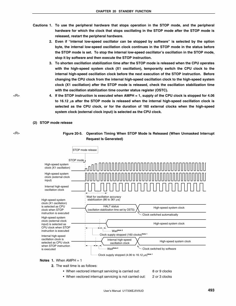
CHAPTER 20 STANDBY FUNCTION
User’s Manual U17336EJ5V0UD 493
Cautions 1. To use the peripheral hardware that stops operation in the STOP mode, and the peripheral
hardware for which the clock that stops oscillating in the STOP mode after the STOP mode is
released, restart the peripheral hardware.
2. Even if “internal low-speed oscillator can be stopped by software” is selected by the option
byte, the internal low-speed oscillation clock continues in the STOP mode in the status before
the STOP mode is set. To stop the internal low-speed oscillator’s oscillation in the STOP mode,
stop it by software and then execute the STOP instruction.
3. To shorten oscillation stabilization time after the STOP mode is released when the CPU operates
with the high-speed system clock (X1 oscillation), temporarily switch the CPU clock to the
internal high-speed oscillation clock before the next execution of the STOP instruction. Before
changing the CPU clock from the internal high-speed oscillation clock to the high-speed system
clock (X1 oscillation) after the STOP mode is released, check the oscillation stabilization time
with the oscillation stabilization time counter status register (OSTC).
4. If the STOP instruction is executed when AMPH = 1, supply of the CPU clock is stopped for 4.06
to 16.12 μs after the STOP mode is released when the internal high-speed oscillation clock is
selected as the CPU clock, or for the duration of 160 external clocks when the high-speed
system clock (external clock input) is selected as the CPU clock.
(2) STOP mode release
Figure 20-5. Operation Timing When STOP Mode Is Released (When Unmasked Interrupt
Request Is Generated)
STOP mode
STOP mode release
High-speed system clock (X1 oscillation)
High-speed system clock (external clock input)
Internal high-speed oscillation clock
High-speed system clock (X1 oscillation)is selected as CPU clock when STOP instruction is executed
High-speed system clock (external clock input) is selected as CPU clock when STOP instruction is executed
Internal high-speed oscillation clock is selected as CPU clock when STOP instruction is executed
Wait for oscillation accuracystabilization (86 to 361 s) μ
HALT status(oscillation stabilization time set by OSTS)
Clock switched automatically
Clock switched by software
High-speed system clock
High-speed system clock
WaitNote 2
WaitNote 2
Clock supply stopped (4.06 to 16.12 s)Note 1
High-speed system clock
μ
Clock supply stopped (160 clocks)Note 1
Internal high-speed oscillation clock
Notes 1. When AMPH = 1
2. The wait time is as follows:
• When vectored interrupt servicing is carried out: 8 or 9 clocks
• When vectored interrupt servicing is not carried out: 2 or 3 clocks
<R>
<R>

CHAPTER 20 STANDBY FUNCTION
User’s Manual U17336EJ5V0UD 494
The STOP mode can be released by the following two sources.
(a) Release by unmasked interrupt request
When an unmasked interrupt request is generated, the STOP mode is released. If interrupt acknowledgment
is enabled, vectored interrupt servicing is carried out. If interrupt acknowledgment is disabled, the next
address instruction is executed.
Figure 20-6. STOP Mode Release by Interrupt Request Generation (1/2)
(1) When high-speed system clock (X1 oscillation) is used as CPU clock
Normal operation(high-speed
system clock)
Normal operation(high-speed
system clock)
OscillatesOscillates
STOPinstruction
STOP mode
Wait(set by OSTS)
Standby release signal
Oscillation stabilization wait(HALT mode status)
Oscillation stoppedHigh-speedsystem clock
(X1 oscillation)
Status of CPU
Oscillation stabilization time (set by OSTS)
Interruptrequest
(2) When high-speed system clock (external clock input) is used as CPU clock (1/2)
• When AMPH = 1 Interruptrequest
STOPinstruction
Standby release signal
Status of CPU
High-speedsystem clock
(external clock input)
Oscillates
Normal operation(high-speed
system clock) STOP mode
Oscillation stopped Oscillates
Normal operation(high-speed
system clock)WaitNoteClock supply
stopped
(160 clocks)
Note The wait time is as follows:
• When vectored interrupt servicing is carried out: 8 or 9 clocks
• When vectored interrupt servicing is not carried out: 2 or 3 clocks
Remark The broken lines indicate the case when the interrupt request that has released the standby mode
is acknowledged.
<R>

CHAPTER 20 STANDBY FUNCTION
User’s Manual U17336EJ5V0UD 495
Figure 20-6. STOP Mode Release by Interrupt Request Generation (2/2)
(2) When high-speed system clock (external clock input) is used as CPU clock (2/2)
• When AMPH = 0 InterruptrequestSTOP
instruction
Standby release signal
Status of CPU
High-speedsystem clock
(external clock input)
Normal operation(high-speed
system clock)
Oscillates
STOP mode
Oscillation stopped
WaitNote
Normal operation(high-speed
system clock)
Oscillates
(3) When internal high-speed oscillation clock is used as CPU clock
• When AMPH = 1
(4.06 to 16.12 s)
Standby release signal
Status of CPU
Internal high-speedoscillation clock
Normal operation(internal high-speed
oscillation clock)
Oscillates
STOP mode
Oscillation stopped
Wait for oscillationaccuracy stabilization
(86 to 361 s)μ
InterruptrequestSTOP
instruction
WaitNote
Normal operation(internal high-speed
oscillation clock)Clock supply
stopped
μOscillates
• When AMPH = 0
WaitNote
Wait for oscillationaccuracy stabilization
(86 to 361 s)
Oscillates
Normal operation(internal high-speed
oscillation clock)STOP mode
Oscillation stoppedOscillates
Normal operation(internal high-speed
oscillation clock)
Internal high-speedoscillation clock
Status of CPU
Standby release signal
STOPinstruction
Interruptrequest
μ
Note The wait time is as follows:
• When vectored interrupt servicing is carried out: 8 or 9 clocks
• When vectored interrupt servicing is not carried out: 2 or 3 clocks
Remark The broken lines indicate the case when the interrupt request that has released the standby mode
is acknowledged.
<R>

CHAPTER 20 STANDBY FUNCTION
User’s Manual U17336EJ5V0UD 496
(b) Release by reset signal generation
When the reset signal is generated, STOP mode is released, and then, as in the case with a normal reset
operation, the program is executed after branching to the reset vector address.
Figure 20-7. STOP Mode Release by Reset
(1) When high-speed system clock is used as CPU clock
STOPinstruction
Reset signal
High-speedsystem clock
(X1 oscillation)
Normal operation(high-speed
system clock) STOP modeResetperiod
Normal operation(internal high-speed
oscillation clock)
OscillatesOscillationstopped Oscillates
Status of CPU
Oscillation stabilization time(211/fX to 216/fX)
Oscillationstopped
Starting X1 oscillation is specified by software.
Oscillation stopped
Resetprocessing(11 to 45 s)μ
(2) When internal high-speed oscillation clock is used as CPU clock
STOPinstruction
Reset signal
Internal high-speedoscillation clock
Normal operation(internal high-speed
oscillation clock) STOP modeResetperiod
Normal operation(internal high-speed
oscillation clock)
OscillatesOscillationstopped
Status of CPU
OscillatesOscillation stopped
Wait for oscillationaccuracy stabilization
(86 to 361 s)
Resetprocessing(11 to 45 s)μ
μ
Remark fX: X1 clock oscillation frequency
Table 20-4. Operation in Response to Interrupt Request in STOP Mode
Release Source MK×× PR×× IE ISP Operation
0 0 0 × Next address
instruction execution
0 0 1 × Interrupt servicing
execution
0 1 0 1
0 1 × 0
Next address
instruction execution
0 1 1 1 Interrupt servicing
execution
Maskable interrupt
request
1 × × × STOP mode held
Reset − − × × Reset processing
×: don’t care

User’s Manual U17336EJ5V0UD 497
CHAPTER 21 RESET FUNCTION
The following four operations are available to generate a reset signal.
(1) External reset input via RESET pin
(2) Internal reset by watchdog timer program loop detection
(3) Internal reset by comparison of supply voltage and detection voltage of power-on-clear (POC) circuit
(4) Internal reset by comparison of supply voltage and detection voltage of low-power-supply detector (LVI)
External and internal resets have no functional differences. In both cases, program execution starts at the address
at 0000H and 0001H when the reset signal is generated.
A reset is applied when a low level is input to the RESET pin, the watchdog timer overflows, or by POC and LVI
circuit voltage detection, and each item of hardware is set to the status shown in Tables 21-1 and 21-2. Each pin is
high impedance during reset signal generation or during the oscillation stabilization time just after a reset release,
except for P130, which is low-level output.
When a low level is input to the RESET pin, the device is reset. It is released from the reset status when a high
level is input to the RESET pin and program execution is started with the internal high-speed oscillation clock after
reset processing. A reset by the watchdog timer is automatically released, and program execution starts using the
internal high-speed oscillation clock (see Figures 21-2 to 21-4) after reset processing. Reset by POC and LVI circuit
power supply detection is automatically released when VDD ≥ VPOC or VDD ≥ VLVI after the reset, and program
execution starts using the internal high-speed oscillation clock (see CHAPTER 22 POWER-ON-CLEAR CIRCUIT
and CHAPTER 23 LOW-VOLTAGE DETECTOR) after reset processing.
Cautions 1. For an external reset, input a low level for 10 μs or more to the RESET pin.
2. During reset input, the X1 clock, XT1 clock, internal high-speed oscillation clock, and internal
low-speed oscillation clock stop oscillating. External main system clock input and external
subsystem clock input become invalid.
3. When the STOP mode is released by a reset, the STOP mode contents are held during reset
input. However, the port pins become high-impedance, except for P130Note, which is set to
low-level output.
Note 48-pin products only.

CH
AP
TE
R 21 R
ES
ET
FU
NC
TIO
N
User’s M
anual U17336E
J5V0U
D
498
Figure 21-1. Block Diagram of Reset Function
LVIRFWDTRF
Reset control flag register (RESF)
Internal bus
Watchdog timer reset signal
RESET
Power-on-clear circuit reset signal
Low-voltage detector reset signal Reset signal
Reset signal to LVIM/LVIS register
Clear
Set
Clear
Set
Caution An LVI circuit internal reset does not reset the LVI circuit.
Remarks 1. LVIM: Low-voltage detection register
2. LVIS: Low-voltage detection level selection register

CHAPTER 21 RESET FUNCTION
User’s Manual U17336EJ5V0UD 499
Figure 21-2. Timing of Reset by RESET Input
Delay Delay(5 s (TYP.))
Hi-Z
Normal operationCPU clock Reset period (oscillation stop)
Normal operation (internal high-speed oscillation clock)
RESET
Internal reset signal
Port pin(except P130Note 1)
Port pin (P130Note 1) Note 2
High-speed system clock(when X1 oscillation is selected)
Internal high-speedoscillation clock
Starting X1 oscillation is specified by software.
Resetprocessing
(11 to 45 s)μ
μ
Wait for oscillationaccuracy stabilization
(86 to 361 s)μ
Remark When reset is effected, P130Note 1 outputs a low level. If P130Note 1 is set to output a high level before reset
is effected, the output signal of P130Note 1 can be dummy-output as the CPU reset signal.
Notes 1. 48-pin products only.
2. Set P130 to high-level output by software.
Figure 21-3. Timing of Reset Due to Watchdog Timer Overflow
Normal operation Reset period (oscillation stop)
CPU clock
Watchdog timeroverflow
Internal reset signal
Hi-Z Port pin(except P130Note 1)
Port pin (P130Note 1) Note 2
High-speed system clock(when X1 oscillation is selected)
Internal high-speedoscillation clock
Starting X1 oscillation is specified by software.
Normal operation (internal high-speed oscillation clock)
Resetprocessing
(11 to 45 s)μ
Wait for oscillationaccuracy stabilization
(86 to 361 s)μ
Caution A watchdog timer internal reset resets the watchdog timer.
Remark When reset is effected, P130Note 1 outputs a low level. If P130Note 1 is set to output a high level before reset
is effected, the output signal of P130Note 1 can be dummy-output as the CPU reset signal.
Notes 1. 48-pin products only.
2. Set P130 to high-level output by software.
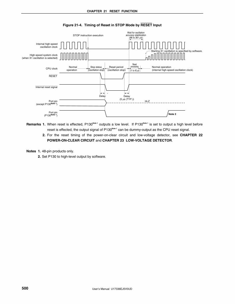
CHAPTER 21 RESET FUNCTION
User’s Manual U17336EJ5V0UD 500
Figure 21-4. Timing of Reset in STOP Mode by RESET Input
Delay
NormaloperationCPU clock
Reset period (oscillation stop)
RESET
Internal reset signal
STOP instruction execution
Stop status (oscillation stop)
High-speed system clock(when X1 oscillation is selected)
Internal high-speedoscillation clock
Hi-Z Port pin(except P130Note 1)
Port pin (P130Note 1) Note 2
Starting X1 oscillation is specified by software.
Normal operation (internal high-speed oscillation clock)
Resetprocessing
(11 to 45 s)
Delay(5 s (TYP.))
μ
μ
Wait for oscillationaccuracy stabilization
(86 to 361 s)μ
Remarks 1. When reset is effected, P130Note 1 outputs a low level. If P130Note 1 is set to output a high level before
reset is effected, the output signal of P130Note 1 can be dummy-output as the CPU reset signal.
2. For the reset timing of the power-on-clear circuit and low-voltage detector, see CHAPTER 22
POWER-ON-CLEAR CIRCUIT and CHAPTER 23 LOW-VOLTAGE DETECTOR.
Notes 1. 48-pin products only.
2. Set P130 to high-level output by software.

CHAPTER 21 RESET FUNCTION
User’s Manual U17336EJ5V0UD 501
Table 21-1. Operation Statuses During Reset Period
Item During Reset Period
System clock Clock supply to the CPU is stopped.
fRH Operation stopped
fX Operation stopped (pin is I/O port mode)
Main system clock
fEXCLK Clock input invalid (pin is I/O port mode)
fXT Operation stopped (pin is I/O port mode)
Subsystem clock
fEXCLKS Clock input invalid (pin is I/O port mode)
fRL
CPU
Flash memory
RAM
Port (latch)
16-bit timer/event counter 00
50 8-bit timer/event
counter 51
H0 8-bit timer
H1
Watch timer
Watchdog timer
Clock outputNote 1
A/D converter
UART0
UART6
CSI10
Serial interface
IIC0
Multiplier/dividerNote 2
Operation stopped
Power-on-clear function Operable
Low-voltage detection function
External interrupt
Operation stopped
Notes 1. 48-pin products only.
2. μPD78F0514, 78F0515, and 78F0515D only.
Remark fRH: Internal high-speed oscillation clock
fX: X1 oscillation clock
fEXCLK: External main system clock
fXT: XT1 oscillation clock
fEXCLKS: External subsystem clock
fRL: Internal low-speed oscillation clock

CHAPTER 21 RESET FUNCTION
User’s Manual U17336EJ5V0UD 502
Table 21-2. Hardware Statuses After Reset Acknowledgment (1/3)
Hardware After Reset AcknowledgmentNote 1
Program counter (PC) The contents of the reset vector table (0000H, 0001H) are set.
Stack pointer (SP) Undefined
Program status word (PSW) 02H
Data memory UndefinedNote 2 RAM
General-purpose registers UndefinedNote 2
Port registers (P0 to P4, P6, P7, P12, P13Note 3, P14Note 3) (output latches) 00H
Port mode registers (PM0 to PM4, PM6, PM7, PM12, PM14Note 3) FFH
Pull-up resistor option registers (PU0, PU1, PU3, PU4, PU7, PU12, PU14Note 3) 00H
Internal expansion RAM size switching register (IXS) 0CHNote 4
Internal memory size switching register (IMS) CFHNote 4
Clock operation mode select register (OSCCTL) 00H
Processor clock control register (PCC) 01H
Internal oscillation mode register (RCM) 80H
Main OSC control register (MOC) 80H
Main clock mode register (MCM) 00H
Oscillation stabilization time counter status register (OSTC) 00H
Oscillation stabilization time select register (OSTS) 05H
Timer counter 00 (TM00) 0000H
Capture/compare registers 000, 010 (CR000, CR010) 0000H
Mode control register 00 (TMC00) 00H
Prescaler mode register 00 (PRM00) 00H
Capture/compare control register 00 (CRC00) 00H
16-bit timer/event counter 00
Timer output control register 00 (TOC00) 00H
Notes 1. During reset signal generation or oscillation stabilization time wait, only the PC contents among the
hardware statuses become undefined. All other hardware statuses remain unchanged after reset.
2. When a reset is executed in the standby mode, the pre-reset status is held even after reset.
3. 48-pin products only.
4. The initial values of the internal memory size switching register (IMS) and internal expansion RAM size
switching register (IXS) after a reset release are constant (IMS = CFH, IXS = 0CH) in all the 78K0/KC2
products, regardless of the internal memory capacity. Therefore, after a reset is released, be sure to set
the following values for each product.
Flash Memory Version (78K0/KC2) IMS IXS
μPD78F0511 04H
μPD78F0512 C6H
μPD78F0513, 78F0513DNote 5 C8H
0CH
μPD78F0514 CCH 0AH
μPD78F0515, 78F0515DNote 5 CFH 08H
5. The ROM and RAM capacities of the products with the on-chip debug function can be debugged by
setting IMS and IXS, according to the debug target products. Set IMS and IXS according to the debug
target products.
<R>

CHAPTER 21 RESET FUNCTION
User’s Manual U17336EJ5V0UD 503
Table 21-2. Hardware Statuses After Reset Acknowledgment (2/3)
Hardware Status After Reset
AcknowledgmentNote 1
Timer counters 50, 51 (TM50, TM51) 00H
Compare registers 50, 51 (CR50, CR51) 00H
Timer clock selection registers 50, 51 (TCL50, TCL51) 00H
8-bit timer/event counters 50, 51
Mode control registers 50, 51 (TMC50, TMC51) 00H
Compare registers 00, 10, 01, 11 (CMP00, CMP10, CMP01, CMP11) 00H
Mode registers (TMHMD0, TMHMD1) 00H
8-bit timers H0, H1
Carrier control register 1 (TMCYC1)Note 2 00H
Watch timer Operation mode register (WTM) 00H
Clock output controllerNote 3
Clock output selection register (CKS) 00H
Watchdog timer Enable register (WDTE) 1AH/9AHNote 4
10-bit A/D conversion result register (ADCR) 0000H
8-bit A/D conversion result register (ADCRH) 00H
Mode register (ADM) 00H
Analog input channel specification register (ADS) 00H
A/D converter
A/D port configuration register (ADPC) 00H
Receive buffer register 0 (RXB0) FFH
Transmit shift register 0 (TXS0) FFH
Asynchronous serial interface operation mode register 0 (ASIM0) 01H
Asynchronous serial interface reception error status register 0 (ASIS0) 00H
Serial interface
UART0
Baud rate generator control register 0 (BRGC0) 1FH
Receive buffer register 6 (RXB6) FFH
Transmit buffer register 6 (TXB6) FFH
Asynchronous serial interface operation mode register 6 (ASIM6) 01H
Asynchronous serial interface reception error status register 6 (ASIS6) 00H
Asynchronous serial interface transmission status register 6 (ASIF6) 00H
Clock selection register 6 (CKSR6) 00H
Baud rate generator control register 6 (BRGC6) FFH
Asynchronous serial interface control register 6 (ASICL6) 16H
Serial interface
UART6
Input switch control register (ISC) 00H
Transmit buffer register 10 (SOTB10) 00H
Serial I/O shift registers 10 (SIO10) 00H
Serial operation mode registers 10 (CSIM10) 00H
Serial interface
CSI10
Serial clock selection registers 10 (CSIC10) 00H
Notes 1. During reset signal generation or oscillation stabilization time wait, only the PC contents among the
hardware statuses become undefined. All other hardware statuses remain unchanged after reset.
2. 8-bit timer H1 only.
3. 48-pin products only.
4. The reset value of WDTE is determined by the option byte setting.
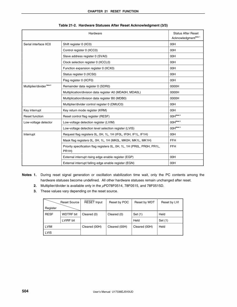
CHAPTER 21 RESET FUNCTION
User’s Manual U17336EJ5V0UD 504
Table 21-2. Hardware Statuses After Reset Acknowledgment (3/3)
Hardware Status After Reset
AcknowledgmentNote 1
Shift register 0 (IIC0) 00H
Control register 0 (IICC0) 00H
Slave address register 0 (SVA0) 00H
Clock selection register 0 (IICCL0) 00H
Function expansion register 0 (IICX0) 00H
Status register 0 (IICS0) 00H
Serial interface IIC0
Flag register 0 (IICF0) 00H
Remainder data register 0 (SDR0) 0000H
Multiplication/division data register A0 (MDA0H, MDA0L) 0000H
Multiplication/division data register B0 (MDB0) 0000H
Multiplier/divider Note 2
Multiplier/divider control register 0 (DMUC0) 00H
Key interrupt Key return mode register (KRM) 00H
Reset function Reset control flag register (RESF) 00HNote 3
Low-voltage detection register (LVIM) 00HNote 3 Low-voltage detector
Low-voltage detection level selection register (LVIS) 00HNote 3
Request flag registers 0L, 0H, 1L, 1H (IF0L, IF0H, IF1L, IF1H) 00H
Mask flag registers 0L, 0H, 1L, 1H (MK0L, MK0H, MK1L, MK1H) FFH
Priority specification flag registers 0L, 0H, 1L, 1H (PR0L, PR0H, PR1L,
PR1H)
FFH
External interrupt rising edge enable register (EGP) 00H
Interrupt
External interrupt falling edge enable register (EGN) 00H
Notes 1. During reset signal generation or oscillation stabilization time wait, only the PC contents among the
hardware statuses become undefined. All other hardware statuses remain unchanged after reset.
2. Multiplier/divider is available only in the μPD78F0514, 78F0515, and 78F0515D.
3. These values vary depending on the reset source.
Reset Source
Register
RESET Input Reset by POC Reset by WDT Reset by LVI
WDTRF bit Set (1) Held RESF
LVIRF bit
Cleared (0) Cleared (0)
Held Set (1)
LVIM
LVIS
Cleared (00H) Cleared (00H) Cleared (00H) Held
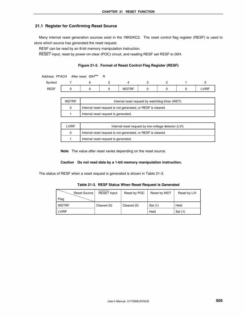
CHAPTER 21 RESET FUNCTION
User’s Manual U17336EJ5V0UD 505
21.1 Register for Confirming Reset Source
Many internal reset generation sources exist in the 78K0/KC2. The reset control flag register (RESF) is used to
store which source has generated the reset request.
RESF can be read by an 8-bit memory manipulation instruction.
RESET input, reset by power-on-clear (POC) circuit, and reading RESF set RESF to 00H.
Figure 21-5. Format of Reset Control Flag Register (RESF)
Address: FFACH After reset: 00HNote R
Symbol 7 6 5 4 3 2 1 0
RESF 0 0 0 WDTRF 0 0 0 LVIRF
WDTRF Internal reset request by watchdog timer (WDT)
0 Internal reset request is not generated, or RESF is cleared.
1 Internal reset request is generated.
LVIRF Internal reset request by low-voltage detector (LVI)
0 Internal reset request is not generated, or RESF is cleared.
1 Internal reset request is generated.
Note The value after reset varies depending on the reset source.
Caution Do not read data by a 1-bit memory manipulation instruction.
The status of RESF when a reset request is generated is shown in Table 21-3.
Table 21-3. RESF Status When Reset Request Is Generated
Reset Source
Flag
RESET Input Reset by POC Reset by WDT Reset by LVI
WDTRF Set (1) Held
LVIRF
Cleared (0) Cleared (0)
Held Set (1)

User’s Manual U17336EJ5V0UD 506
CHAPTER 22 POWER-ON-CLEAR CIRCUIT
22.1 Functions of Power-on-Clear Circuit
The power-on-clear circuit (POC) has the following functions.
• Generates internal reset signal at power on.
In the 1.59 V POC mode (option byte: POCMODE = 0), the reset signal is released when the supply voltage
(VDD) exceeds 1.59 V ±0.15 V.
In the 2.7 V/1.59 V POC mode (option byte: POCMODE = 1), the reset signal is released when the supply
voltage (VDD) exceeds 2.7 V ±0.2 V.
• Compares supply voltage (VDD) and detection voltage (VPOC = 1.59 V ±0.15 V), generates internal reset signal
when VDD < VPOC.
Caution If an internal reset signal is generated in the POC circuit, the reset control flag register (RESF)
is cleared to 00H.
Remark The 78K0/KC2 incorporates multiple hardware functions that generate an internal reset signal. A flag
that indicates the reset source is located in the reset control flag register (RESF) for when an internal
reset signal is generated by the watchdog timer (WDT) or low-voltage-detector (LVI). RESF is not
cleared to 00H and the flag is set to 1 when an internal reset signal is generated by WDT or LVI.
For details of RESF, see CHAPTER 21 RESET FUNCTION.
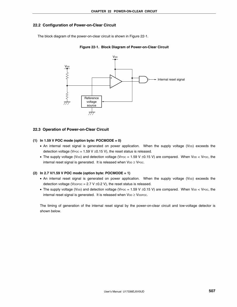
CHAPTER 22 POWER-ON-CLEAR CIRCUIT
User’s Manual U17336EJ5V0UD 507
22.2 Configuration of Power-on-Clear Circuit
The block diagram of the power-on-clear circuit is shown in Figure 22-1.
Figure 22-1. Block Diagram of Power-on-Clear Circuit
−
+
Referencevoltagesource
Internal reset signal
VDD
VDD
22.3 Operation of Power-on-Clear Circuit
(1) In 1.59 V POC mode (option byte: POCMODE = 0)
• An internal reset signal is generated on power application. When the supply voltage (VDD) exceeds the
detection voltage (VPOC = 1.59 V ±0.15 V), the reset status is released.
• The supply voltage (VDD) and detection voltage (VPOC = 1.59 V ±0.15 V) are compared. When VDD < VPOC, the
internal reset signal is generated. It is released when VDD ≥ VPOC.
(2) In 2.7 V/1.59 V POC mode (option byte: POCMODE = 1)
• An internal reset signal is generated on power application. When the supply voltage (VDD) exceeds the
detection voltage (VDDPOC = 2.7 V ±0.2 V), the reset status is released.
• The supply voltage (VDD) and detection voltage (VPOC = 1.59 V ±0.15 V) are compared. When VDD < VPOC, the
internal reset signal is generated. It is released when VDD ≥ VDDPOC.
The timing of generation of the internal reset signal by the power-on-clear circuit and low-voltage detector is
shown below.

CHAPTER 22 POWER-ON-CLEAR CIRCUIT
User’s Manual U17336EJ5V0UD 508
Figure 22-2. Timing of Generation of Internal Reset Signal by Power-on-Clear Circuit
and Low-Voltage Detector (1/2)
(1) In 1.59 V POC mode (option byte: POCMODE = 0)
Note 4 Note 4
Internal high-speedoscillation clock (fRH)
High-speedsystem clock (fXH)
(when X1 oscillation is selected)
Starting oscillation isspecified by software.
VPOC = 1.59 V (TYP.)
VLVI
Operationstops
Wait for voltagestabilization
(1.93 to 5.39 ms)
Normal operation (internal high-speedoscillation clock)Note 5
Operation stops
Reset period(oscillation
stop)
Reset period(oscillation
stop)
Wait for oscillationaccuracy stabilization(86 to 361 s)
Normal operation (internal high-speedoscillation clock)Note 5
Starting oscillation isspecified by software.
Starting oscillation isspecified by software.
CPU
0 V
Supply voltage(VDD)
1.8 VNotes 1, 2, 3
Wait for voltagestabilization
(1.93 to 5.39 ms)
Normal operation (internal high-speedoscillation clock)Note 5
0.5 V/ms (MIN.)Notes 2, 3
Set LVI to be used for reset
Set LVI to be used for reset
Set LVI to be used for interrupt
Internal reset signal
Reset processing (11 to 45 s)μ Reset processing (11 to 45 s)μ Reset processing (11 to 45 s)μ
μ
Notes 1. The guaranteed operation range for the standard and (A) grade products is 1.8 V ≤ VDD ≤ 5.5 V, and
2.7 V ≤ VDD ≤ 5.5 V for the (A2) grade products. To set the voltage range below the guaranteed
operation range to the reset state when the supply voltage falls, use the reset function of the low-
voltage detector, or input a low level to the RESET pin.
2. With the standard and (A) grade products, if the voltage rises to 1.8 V at a rate slower than 0.5 V/ms
(MIN.) on power application, input a low level to the RESET pin after power application and before the
voltage reaches 1.8 V, or set the 2.7 V/1.59 V POC mode by using an option byte (POCMODE = 1).
3. With the (A2) grade products, if the voltage rises to 2.7 V at a rate slower than 0.75 V/ms (MIN.) on
power application, input a low level to the RESET pin after power application and before the voltage
reaches 2.7 V.
4. The oscillation accuracy stabilization time of the internal high-speed oscillation clock is included in the
internal voltage stabilization time.
5. The CPU clock can be switched from the internal high-speed oscillation clock to the high-speed system
clock or to the subsystem clock. To use the X1 clock, use the OSTC register to confirm the lapse of
the oscillation stabilization time. To use the XT1 clock, use the timer function for confirmation of the
lapse of the stabilization time.
Caution Set the low-voltage detector by software after the reset status is released (see CHAPTER 23
LOW-VOLTAGE DETECTOR).
Remark VLVI: LVI detection voltage
VPOC: POC detection voltage
<R>
<R>
<R>

CHAPTER 22 POWER-ON-CLEAR CIRCUIT
User’s Manual U17336EJ5V0UD 509
Figure 22-2. Timing of Generation of Internal Reset Signal by Power-on-Clear Circuit
and Low-Voltage Detector (2/2)
(2) In 2.7 V/1.59 V POC mode (option byte: POCMODE = 1)
Internal high-speedoscillation clock (fRH)
High-speedsystem clock (fXH)
(when X1 oscillation is selected)
Starting oscillation isspecified by software.
Internal reset signal
VDDPOC = 2.7 V (TYP.)
VPOC = 1.59 V (TYP.)
VLVI
Operationstops
Normal operation (internal high-speedoscillation clock)Note 2
Normal operation (internal high-speedoscillation clock)Note 2
Operation stops
Reset period(oscillation
stop)
Reset period(oscillation
stop)
Normal operation (internal high-speedoscillation clock)Note 2
Starting oscillation isspecified by software.
Starting oscillation isspecified by software.
CPU
0 V
Supply voltage(VDD)
1.8 VNote 1
Reset processing (11 to 45 s)μ Reset processing (11 to 45 s)μ Reset processing (11 to 45 s)μ
Set LVI to be used for reset
Set LVI to be used for reset
Set LVI to be used for interrupt
Wait for oscillationaccuracy stabilization(86 to 361 s)μ
Wait for oscillationaccuracy stabilization(86 to 361 s)μ
Wait for oscillationaccuracy stabilization(86 to 361 s)μ
Notes 1. The guaranteed operation range for the standard and (A) grade products is 1.8 V ≤ VDD ≤ 5.5 V, and
2.7 V ≤ VDD ≤ 5.5 V for the (A2) grade products. To set the voltage range below the guaranteed
operation range to the reset state when the supply voltage falls, use the reset function of the low-
voltage detector, or input a low level to the RESET pin.
2. The CPU clock can be switched from the internal high-speed oscillation clock to the high-speed system
clock or to the subsystem clock. To use the X1 clock, use the OSTC register to confirm the lapse of
the oscillation stabilization time. To use the XT1 clock, use the timer function for confirmation of the
lapse of the stabilization time.
Cautions 1. Set the low-voltage detector by software after the reset status is released (see CHAPTER 23
LOW-VOLTAGE DETECTOR).
2. A voltage oscillation stabilization time of 1.93 to 5.39 ms is required after the supply voltage
reaches 1.59 V (TYP.). If the supply voltage rises from 1.59 V (TYP.) to 2.7 V (TYP.) within 1.93
ms, the power supply oscillation stabilization time of 0 to 5.39 ms is automatically generated
before reset processing.
Remark VLVI: LVI detection voltage
VPOC: POC detection voltage
<R>

CHAPTER 22 POWER-ON-CLEAR CIRCUIT
User’s Manual U17336EJ5V0UD 510
22.4 Cautions for Power-on-Clear Circuit
In a system where the supply voltage (VDD) fluctuates for a certain period in the vicinity of the POC detection
voltage (VPOC), the system may be repeatedly reset and released from the reset status. In this case, the time from
release of reset to the start of the operation of the microcontroller can be arbitrarily set by taking the following action.
<Action>
After releasing the reset signal, wait for the supply voltage fluctuation period of each system by means of a
software counter that uses a timer, and then initialize the ports.
Figure 22-3. Example of Software Processing After Reset Release (1/2)
• If supply voltage fluctuation is 50 ms or less in vicinity of POC detection voltage
; Check the reset sourceNote 2
Initialize the port.
Note 1
Reset
Initializationprocessing <1>
50 ms has passed?(TMIFH1 = 1?)
Initializationprocessing <2>
Setting 8-bit timer H1(to measure 50 ms)
; Setting of division ratio of system clock, such as setting of timer or A/D converter
Yes
No
Power-on-clear
Clearing WDT
; fPRS = Internal high-speed oscillation clock (8.4 MHz (MAX.)) (default)Source: fPRS (8.4 MHz (MAX.))/212,
where comparison value = 102: ≅ 50 msTimer starts (TMHE1 = 1).
Notes 1. If reset is generated again during this period, initialization processing <2> is not started.
2. A flowchart is shown on the next page.

CHAPTER 22 POWER-ON-CLEAR CIRCUIT
User’s Manual U17336EJ5V0UD 511
Figure 22-3. Example of Software Processing After Reset Release (2/2)
• Checking reset source
Yes
No
Check reset source
Power-on-clear/externalreset generated
Reset processing bywatchdog timer
Reset processing bylow-voltage detector
No
WDTRF of RESFregister = 1?
LVIRF of RESFregister = 1?
Yes

User’s Manual U17336EJ5V0UD 512
CHAPTER 23 LOW-VOLTAGE DETECTOR
23.1 Functions of Low-Voltage Detector
The low-voltage detector (LVI) has the following functions.
• The LVI circuit compares the supply voltage (VDD) with the detection voltage (VLVI) or the input voltage from an
external input pin (EXLVI) with the detection voltage (VEXLVI = 1.21 V (TYP.): fixed), and generates an internal
reset or internal interrupt signal.
• The supply voltage (VDD) or input voltage from an external input pin (EXLVI) can be selected by software.
• Reset or interrupt function can be selected by software.
• Detection levels (16 levels) of supply voltage can be changed by software.
• Operable in STOP mode.
The reset and interrupt signals are generated as follows depending on selection by software.
Selection of Level Detection of Supply Voltage (VDD)
(LVISEL = 0)
Selection Level Detection of Input Voltage from
External Input Pin (EXLVI) (LVISEL = 1)
Selects reset (LVIMD = 1). Selects interrupt (LVIMD = 0). Selects reset (LVIMD = 1). Selects interrupt (LVIMD = 0).
Generates an internal reset
signal when VDD < VLVI and
releases the reset signal when
VDD ≥ VLVI.
Generates an internal interrupt
signal when VDD drops lower
than VLVI (VDD < VLVI) or when
VDD becomes VLVI or higher
(VDD ≥ VLVI).
Generates an internal reset
signal when EXLVI < VEXLVI
and releases the reset signal
when EXLVI ≥ VEXLVI.
Generates an internal interrupt
signal when EXLVI drops
lower than VEXLVI (EXLVI <
VEXLVI) or when EXLVI
becomes VEXLVI or higher
(EXLVI ≥ VEXLVI).
Remark LVISEL: Bit 2 of low-voltage detection register (LVIM)
LVIMD: Bit 1 of LVIM
While the low-voltage detector is operating, whether the supply voltage or the input voltage from an external input
pin is more than or less than the detection level can be checked by reading the low-voltage detection flag (LVIF: bit 0
of LVIM).
When the low-voltage detector is used to reset, bit 0 (LVIRF) of the reset control flag register (RESF) is set to 1 if
reset occurs. For details of RESF, see CHAPTER 21 RESET FUNCTION.

CHAPTER 23 LOW-VOLTAGE DETECTOR
User’s Manual U17336EJ5V0UD 513
23.2 Configuration of Low-Voltage Detector
The block diagram of the low-voltage detector is shown in Figure 23-1.
Figure 23-1. Block Diagram of Low-Voltage Detector
LVIS1 LVIS0 LVION
−
+
Referencevoltagesource
VDD
Internal bus
N-ch
Low-voltage detection level selection register (LVIS)
Low-voltage detection register(LVIM)
LVIS2LVIS3 LVIF
INTLVI
Internal reset signal
4
LVISEL
EXLVI/P120/INTP0
LVIMD
VDDLo
w-v
olta
ge d
etec
tion
leve
l sel
ecto
r
Sel
ecto
r
Sel
ecto
r
23.3 Registers Controlling Low-Voltage Detector
The low-voltage detector is controlled by the following registers.
• Low-voltage detection register (LVIM)
• Low-voltage detection level selection register (LVIS)
• Port mode register 12 (PM12)
(1) Low-voltage detection register (LVIM)
This register sets low-voltage detection and the operation mode.
This register can be set by a 1-bit or 8-bit memory manipulation instruction.
The generation of a reset signal other than an LVI reset clears this register to 00H.
<R>

CHAPTER 23 LOW-VOLTAGE DETECTOR
User’s Manual U17336EJ5V0UD 514
Figure 23-2. Format of Low-Voltage Detection Register (LVIM)
<0>
LVIF
<1>
LVIMD
<2>
LVISEL
3
0
4
0
5
0
6
0
<7>
LVION
Symbol
LVIM
Address: FFBEH After reset: 00HNote 1 R/WNote 2
LVIONNotes 3, 4 Enables low-voltage detection operation
0 Disables operation
1 Enables operation
LVISELNote 3 Voltage detection selection
0 Detects level of supply voltage (VDD)
1 Detects level of input voltage from external input pin (EXLVI)
LVIMDNote 3 Low-voltage detection operation mode (interrupt/reset) selection
0 • LVISEL = 0: Generates an internal interrupt signal when the supply voltage (VDD) drops
lower than the detection voltage (VLVI) (VDD < VLVI) or when VDD becomes
VLVI or higher (VDD ≥ VLVI).
• LVISEL = 1: Generates an interrupt signal when the input voltage from an external
input pin (EXLVI) drops lower than the detection voltage (VEXLVI) (EXLVI <
VEXLVI) or when EXLVI becomes VEXLVI or higher (EXLVI ≥ VEXLVI).
1 • LVISEL = 0: Generates an internal reset signal when the supply voltage (VDD) <
detection voltage (VLVI) and releases the reset signal when VDD ≥ VLVI.
• LVISEL = 1: Generates an internal reset signal when the input voltage from an
external input pin (EXLVI) < detection voltage (VEXLVI) and releases the
reset signal when EXLVI ≥ VEXLVI.
LVIFNote 4 Low-voltage detection flag
0 • LVISEL = 0: Supply voltage (VDD) ≥ detection voltage (VLVI), or when operation is
disabled
• LVISEL = 1: Input voltage from external input pin (EXLVI) ≥ detection voltage (VEXLVI),
or when operation is disabled
1 • LVISEL = 0: Supply voltage (VDD) < detection voltage (VLVI)
• LVISEL = 1: Input voltage from external input pin (EXLVI) < detection voltage (VEXLVI)
Notes 1. This bit is cleared to 00H upon a reset other than an LVI reset.
2. Bit 0 is read-only.
3. LVION, LVIMD, and LVISEL are cleared to 0 in the case of a reset other than an LVI reset.
These are not cleared to 0 in the case of an LVI reset.
4. When LVION is set to 1, operation of the comparator in the LVI circuit is started. Use
software to wait for an operation stabilization time (10 μs (MAX.)) from when LVION is set to 1
until operation is stabilized. After operation has stabilized, 200 μs (MIN.) are required from
when a state below LVI detection voltage has been entered, until LVIF is set (1).
Cautions 1. To stop LVI, follow either of the procedures below.
• When using 8-bit memory manipulation instruction: Write 00H to LVIM.
• When using 1-bit memory manipulation instruction: Clear LVION to 0.
2. Input voltage from external input pin (EXLVI) must be EXLVI < VDD.
3. After an LVI reset has been generated, do not write values to LVIS and LVIM when
LVION = 1.
4. When using LVI as an interrupt, if LVION is cleared (0) in a state below the LVI
detection voltage, an INTLVI signal is generated and LVIIF becomes 1.
<R>
<R>
<R>
<R>

CHAPTER 23 LOW-VOLTAGE DETECTOR
User’s Manual U17336EJ5V0UD 515
(2) Low-voltage detection level selection register (LVIS)
This register selects the low-voltage detection level.
This register can be set by a 1-bit or 8-bit memory manipulation instruction.
The generation of a reset signal other than an LVI reset clears this register to 00H.
Figure 23-3. Format of Low-Voltage Detection Level Selection Register (LVIS)
0
LVIS0
1
LVIS1
2
LVIS2
3
LVIS3
4
0
5
0
6
0
7
0
Symbol
LVIS
Address: FFBFH After reset: 00HNote 1 R/W
LVIS3 LVIS2 LVIS1 LVIS0 Detection level
0 0 0 0 VLVI0 (4.24 V ±0.1 V)
0 0 0 1 VLVI1 (4.09 V ±0.1 V)
0 0 1 0 VLVI2 (3.93 V ±0.1 V)
0 0 1 1 VLVI3 (3.78 V ±0.1 V)
0 1 0 0 VLVI4 (3.62 V ±0.1 V)
0 1 0 1 VLVI5 (3.47 V ±0.1 V)
0 1 1 0 VLVI6 (3.32 V ±0.1 V)
0 1 1 1 VLVI7 (3.16 V ±0.1 V)
1 0 0 0 VLVI8 (3.01 V ±0.1 V)
1 0 0 1 VLVI9 (2.85 V ±0.1 V)
1 0 1 0 VLVI10 (2.70 V ±0.1 V)Note 2
1 0 1 1 VLVI11 (2.55 V ±0.1 V)Note 2
1 1 0 0 VLVI12 (2.39 V ±0.1 V)Note 2
1 1 0 1 VLVI13 (2.24 V ±0.1 V)Note 2
1 1 1 0 VLVI14 (2.08 V ±0.1 V)Note 2
1 1 1 1 VLVI15 (1.93 V ±0.1 V)Note 2
Notes 1. The value of LVIS is not reset but retained as is, upon a reset by LVI. It is cleared to 00H
upon other resets.
2. Do not set VLVI10 to VLVI15 for (A2) grade products.
Cautions 1. Be sure to clear bits 4 to 7 to “0”.
2. Do not change the value of LVIS during LVI operation.
3. When an input voltage from the external input pin (EXLVI) is detected, the detection
voltage (VEXLVI = 1.21 V (TYP.)) is fixed. Therefore, setting of LVIS is not necessary.
4. After an LVI reset has been generated, do not write values to LVIS and LVIM when
LVION = 1.
<R>
<R>
<R>
<R>

CHAPTER 23 LOW-VOLTAGE DETECTOR
User’s Manual U17336EJ5V0UD 516
(3) Port mode register 12 (PM12)
When using the P120/EXLVI/INTP0 pin for external low-voltage detection potential input, set PM120 to 1. At this
time, the output latch of P120 may be 0 or 1.
PM12 can be set by a 1-bit or 8-bit memory manipulation instruction.
Reset signal generation sets PM12 to FFH.
Figure 23-4. Format of Port Mode Register 12 (PM12)
0
PM120
1
PM121
2
PM122
3
PM123
4
PM124
5
1
6
1
7
1
Symbol
PM12
Address: FF2CH After reset: FFH R/W
PM12n P12n pin I/O mode selection (n = 0 to 4)
0 Output mode (output buffer on)
1 Input mode (output buffer off)
23.4 Operation of Low-Voltage Detector
The low-voltage detector can be used in the following two modes.
(1) Used as reset (LVIMD = 1)
• If LVISEL = 0, compares the supply voltage (VDD) and detection voltage (VLVI), generates an internal reset
signal when VDD < VLVI, and releases internal reset when VDD ≥ VLVI.
• If LVISEL = 1, compares the input voltage from external input pin (EXLVI) and detection voltage (VEXLVI = 1.21
V (TYP.)), generates an internal reset signal when EXLVI < VEXLVI, and releases internal reset when EXLVI ≥
VEXLVI.
(2) Used as interrupt (LVIMD = 0)
• If LVISEL = 0, compares the supply voltage (VDD) and detection voltage (VLVI). When VDD drops lower than
VLVI (VDD < VLVI) or when VDD becomes VLVI or higher (VDD ≥ VLVI), generates an interrupt signal (INTLVI).
• If LVISEL = 1, compares the input voltage from external input pin (EXLVI) and detection voltage (VEXLVI = 1.21
V (TYP.)). When EXLVI drops lower than VEXLVI (EXLVI < VEXLVI) or when EXLVI becomes VEXLVI or higher
(EXLVI ≥ VEXLVI), generates an interrupt signal (INTLVI).
While the low-voltage detector is operating, whether the supply voltage or the input voltage from an external input
pin is more than or less than the detection level can be checked by reading the low-voltage detection flag (LVIF: bit 0
of LVIM).
Remark LVIMD: Bit 1 of low-voltage detection register (LVIM)
LVISEL: Bit 2 of LVIM

CHAPTER 23 LOW-VOLTAGE DETECTOR
User’s Manual U17336EJ5V0UD 517
23.4.1 When used as reset
(1) When detecting level of supply voltage (VDD)
• When starting operation
<1> Mask the LVI interrupt (LVIMK = 1).
<2> Clear bit 2 (LVISEL) of the low-voltage detection register (LVIM) to 0 (detects level of supply voltage
(VDD)) (default value).
<3> Set the detection voltage using bits 3 to 0 (LVIS3 to LVIS0) of the low-voltage detection level selection
register (LVIS).
<4> Set bit 7 (LVION) of LVIM to 1 (enables LVI operation).
<5> Use software to wait for an operation stabilization time (10 μs (MAX.)).
<6> Wait until it is checked that (supply voltage (VDD) ≥ detection voltage (VLVI)) by bit 0 (LVIF) of LVIM.
<7> Set bit 1 (LVIMD) of LVIM to 1 (generates reset when the level is detected).
Figure 23-5 shows the timing of the internal reset signal generated by the low-voltage detector. The numbers
in this timing chart correspond to <1> to <7> above.
Cautions 1. <1> must always be executed. When LVIMK = 0, an interrupt may occur immediately
after the processing in <4>.
2. If supply voltage (VDD) ≥ detection voltage (VLVI) when LVIMD is set to 1, an internal reset
signal is not generated.
• When stopping operation
Either of the following procedures must be executed.
• When using 8-bit memory manipulation instruction:
Write 00H to LVIM.
• When using 1-bit memory manipulation instruction:
Clear LVIMD to 0 and then LVION to 0.

CHAPTER 23 LOW-VOLTAGE DETECTOR
User’s Manual U17336EJ5V0UD 518
Figure 23-5. Timing of Low-Voltage Detector Internal Reset Signal Generation
(Detects Level of Supply Voltage (VDD)) (1/2)
(1) In 1.59 V POC mode (option byte: POCMODE = 0)
Supply voltage (VDD)
<3>
<1>
Time
LVIMK flag(set by software)
LVIF flag
LVIRF flagNote 3
Note 2
LVI reset signal
POC reset signal
Internal reset signal
Cleared bysoftware
Not cleared Not cleared
Not cleared Not cleared
Cleared bysoftware
<4>
<7>
Clear
Clear
Clear
<5> Wait time
LVION flag(set by software)
LVIMD flag(set by software)
HNote 1
LLVISEL flag
(set by software)
<6>
<2>
VLVI
VPOC = 1.59 V (TYP.)
Notes 1. The LVIMK flag is set to “1” by reset signal generation.
2. The LVIF flag may be set (1).
3. LVIRF is bit 0 of the reset control flag register (RESF). For details of RESF, see CHAPTER 21
RESET FUNCTION.
Remark <1> to <7> in Figure 23-5 above correspond to <1> to <7> in the description of “When starting
operation” in 23.4.1 (1) When detecting level of supply voltage (VDD).

CHAPTER 23 LOW-VOLTAGE DETECTOR
User’s Manual U17336EJ5V0UD 519
Figure 23-5. Timing of Low-Voltage Detector Internal Reset Signal Generation
(Detects Level of Supply Voltage (VDD)) (2/2)
(2) In 2.7 V/1.59 V POC mode (option byte: POCMODE = 1)
Supply voltage (VDD)
VLVI
<3>
<1>
Time
LVIMK flag(set by software)
LVIF flag
LVIRF flagNote 3
Note 2
LVI reset signal
POC reset signal
Internal reset signal
Cleared bysoftware
Not cleared Not cleared
Not cleared Not cleared
Cleared bysoftware
<4>
<7>
Clear
Clear
Clear
<5> Wait time
LVION flag(set by software)
LVIMD flag(set by software)
HNote 1
LLVISEL flag
(set by software)
<6>
<2>
2.7 V (TYP.)VPOC = 1.59 V (TYP.)
Notes 1. The LVIMK flag is set to “1” by reset signal generation.
2. The LVIF flag may be set (1).
3. LVIRF is bit 0 of the reset control flag register (RESF). For details of RESF, see CHAPTER 21
RESET FUNCTION.
Remark <1> to <7> in Figure 23-5 above correspond to <1> to <7> in the description of “When starting
operation” in 23.4.1 (1) When detecting level of supply voltage (VDD).
CHAPTER 23 LOW-VOLTAGE DETECTOR
User’s Manual U17336EJ5V0UD 520
(2) When detecting level of input voltage from external input pin (EXLVI)
• When starting operation
<1> Mask the LVI interrupt (LVIMK = 1).
<2> Set bit 2 (LVISEL) of the low-voltage detection register (LVIM) to 1 (detects level of input voltage from
external input pin (EXLVI)).
<3> Set bit 7 (LVION) of LVIM to 1 (enables LVI operation).
<4> Use software to wait for an operation stabilization time (10 μs (MAX.)).
<5> Wait until it is checked that (input voltage from external input pin (EXLVI) ≥ detection voltage (VEXLVI =
1.21 V (TYP.))) by bit 0 (LVIF) of LVIM.
<6> Set bit 1 (LVIMD) of LVIM to 1 (generates reset signal when the level is detected).
Figure 23-6 shows the timing of the internal reset signal generated by the low-voltage detector. The numbers
in this timing chart correspond to <1> to <6> above.
Cautions 1. <1> must always be executed. When LVIMK = 0, an interrupt may occur immediately
after the processing in <3>.
2. If input voltage from external input pin (EXLVI) ≥ detection voltage (VEXLVI = 1.21 V (TYP.))
when LVIMD is set to 1, an internal reset signal is not generated.
3. Input voltage from external input pin (EXLVI) must be EXLVI < VDD.
• When stopping operation
Either of the following procedures must be executed.
• When using 8-bit memory manipulation instruction:
Write 00H to LVIM.
• When using 1-bit memory manipulation instruction:
Clear LVIMD to 0 and then LVION to 0.

CHAPTER 23 LOW-VOLTAGE DETECTOR
User’s Manual U17336EJ5V0UD 521
Figure 23-6. Timing of Low-Voltage Detector Internal Reset Signal Generation
(Detects Level of Input Voltage from External Input Pin (EXLVI))
Input voltage fromexternal input pin (EXLVI)
LVI detection voltage(VEXLVI)
<1>
Time
LVIMK flag(set by software)
LVIF flag
LVIRF flagNote 3
Note 2
LVI reset signal
Internal reset signal
Cleared bysoftware
Not cleared Not cleared
Not cleared Not cleared
Cleared bysoftware
<3>
<6>
LVION flag(set by software)
LVIMD flag(set by software)
HNote 1
LVISEL flag(set by software)
<5>
<2>Not clearedNot cleared
<4> Wait time
Not cleared
Not cleared
Not cleared
Notes 1. The LVIMK flag is set to “1” by reset signal generation.
2. The LVIF flag may be set (1).
3. LVIRF is bit 0 of the reset control flag register (RESF). For details of RESF, see CHAPTER 21
RESET FUNCTION.
Remark <1> to <6> in Figure 23-6 above correspond to <1> to <6> in the description of “When starting
operation” in 23.4.1 (2) When detecting level of input voltage from external input pin (EXLVI).

CHAPTER 23 LOW-VOLTAGE DETECTOR
User’s Manual U17336EJ5V0UD 522
23.4.2 When used as interrupt
(1) When detecting level of supply voltage (VDD)
• When starting operation
<1> Mask the LVI interrupt (LVIMK = 1).
<2> Clear bit 2 (LVISEL) of the low-voltage detection register (LVIM) to 0 (detects level of supply voltage
(VDD)) (default value).
<3> Set the detection voltage using bits 3 to 0 (LVIS3 to LVIS0) of the low-voltage detection level selection
register (LVIS).
<4> Set bit 7 (LVION) of LVIM to 1 (enables LVI operation).
<5> Use software to wait for an operation stabilization time (10 μs (MAX.)).
<6> Confirm that “supply voltage (VDD) ≥ detection voltage (VLVI)” when detecting the falling edge of VDD, or
“supply voltage (VDD) < detection voltage (VLVI)” when detecting the rising edge of VDD, at bit 0 (LVIF) of
LVIM.
<7> Clear the interrupt request flag of LVI (LVIIF) to 0.
<8> Release the interrupt mask flag of LVI (LVIMK).
<9> Clear bit 1 (LVIMD) of LVIM to 0 (generates interrupt signal when the level is detected) (default value).
<10> Execute the EI instruction (when vector interrupts are used).
Figure 23-7 shows the timing of the interrupt signal generated by the low-voltage detector. The numbers in
this timing chart correspond to <1> to <9> above.
• When stopping operation
Either of the following procedures must be executed.
• When using 8-bit memory manipulation instruction:
Write 00H to LVIM.
• When using 1-bit memory manipulation instruction:
Clear LVION to 0.

CHAPTER 23 LOW-VOLTAGE DETECTOR
User’s Manual U17336EJ5V0UD 523
Figure 23-7. Timing of Low-Voltage Detector Interrupt Signal Generation
(Detects Level of Supply Voltage (VDD)) (1/2)
(1) In 1.59 V POC mode (option byte: POCMODE = 0)
Supply voltage (VDD)
Time
<1>Note 1 <8> Cleared by software
LVIMK flag(set by software)
LVIF flag
INTLVI
LVIIF flag
Internal reset signal
<4>
<6>
<7> Cleared by software
<5> Wait time
LVION flag(set by software)
Note 2
Note 2
<3>L
LVISEL flag(set by software)
<2>
LVIMD flag(set by software) L
<9>
VLVI
VPOC = 1.59 V (TYP.)
Note 2
Note 3 Note 3
Notes 1. The LVIMK flag is set to “1” by reset signal generation.
2. The interrupt request signal (INTLVI) is generated and the LVIF and LVIIF flags may be set (1).
3. If LVION is cleared (0) in a state below the LVI detection voltage, an INTLVI signal is generated and
LVIIF becomes 1.
Remark <1> to <9> in Figure 23-7 above correspond to <1> to <9> in the description of “When starting
operation” in 23.4.2 (1) When detecting level of supply voltage (VDD).
<R>

CHAPTER 23 LOW-VOLTAGE DETECTOR
User’s Manual U17336EJ5V0UD 524
Figure 23-7. Timing of Low-Voltage Detector Interrupt Signal Generation
(Detects Level of Supply Voltage (VDD)) (2/2)
(2) In 2.7 V/1.59 V POC mode (option byte: POCMODE = 1)
Supply voltage (VDD)
Time
<1>Note 1 <8> Cleared by software
LVIMK flag(set by software)
LVIF flag
INTLVI
LVIIF flag
Internal reset signal
<4>
<6>
<7> Cleared by software
<5> Wait time
LVION flag(set by software)
Note 2
Note 2
<3>L
LVISEL flag(set by software)
<2>
LVIMD flag(set by software) L
<9>
VLVI
2.7 V(TYP.)VPOC = 1.59 V (TYP.)
Note 2
Note 3 Note 3
Notes 1. The LVIMK flag is set to “1” by reset signal generation.
2. The interrupt request signal (INTLVI) is generated and the LVIF and LVIIF flags may be set (1).
3. If LVION is cleared (0) in a state below the LVI detection voltage, an INTLVI signal is generated and
LVIIF becomes 1.
Remark <1> to <9> in Figure 23-7 above correspond to <1> to <9> in the description of “When starting
operation” in 23.4.2 (1) When detecting level of supply voltage (VDD).
<R>
CHAPTER 23 LOW-VOLTAGE DETECTOR
User’s Manual U17336EJ5V0UD 525
(2) When detecting level of input voltage from external input pin (EXLVI)
• When starting operation
<1> Mask the LVI interrupt (LVIMK = 1).
<2> Set bit 2 (LVISEL) of the low-voltage detection register (LVIM) to 1 (detects level of input voltage from
external input pin (EXLVI)).
<3> Set bit 7 (LVION) of LVIM to 1 (enables LVI operation).
<4> Use software to wait for an operation stabilization time (10 μs (MAX.)).
<5> Confirm that “input voltage from external input pin (EXLVI) ≥ detection voltage (VEXLVI = 1.21 V (TYP.)”
when detecting the falling edge of EXLVI, or “input voltage from external input pin (EXLVI) < detection
voltage (VEXLVI = 1.21 V (TYP.)” when detecting the rising edge of EXLVI, at bit 0 (LVIF) of LVIM.
<6> Clear the interrupt request flag of LVI (LVIIF) to 0.
<7> Release the interrupt mask flag of LVI (LVIMK).
<8> Clear bit 1 (LVIMD) of LVIM to 0 (generates interrupt signal when the level is detected) (default value).
<9> Execute the EI instruction (when vector interrupts are used).
Figure 23-8 shows the timing of the interrupt signal generated by the low-voltage detector. The numbers in
this timing chart correspond to <1> to <8> above.
Caution Input voltage from external input pin (EXLVI) must be EXLVI < VDD.
• When stopping operation
Either of the following procedures must be executed.
• When using 8-bit memory manipulation instruction:
Write 00H to LVIM.
• When using 1-bit memory manipulation instruction:
Clear LVION to 0.

CHAPTER 23 LOW-VOLTAGE DETECTOR
User’s Manual U17336EJ5V0UD 526
Figure 23-8. Timing of Low-Voltage Detector Interrupt Signal Generation
(Detects Level of Input Voltage from External Input Pin (EXLVI))
Input voltage from
external input pin (EXLVI)
VEXLVI
Time
<1>Note 1 <7> Cleared by software
LVIMK flag(set by software)
LVIF flag
INTLVI
LVIIF flag
<3>
<5>
<6> Cleared by software
<4> Wait time
LVION flag(set by software)
Note 2
Note 2
LVISEL flag(set by software)
<2>
LVIMD flag(set by software) L
<8>
Note 2
Note 3 Note 3
Notes 1. The LVIMK flag is set to “1” by reset signal generation.
2. The interrupt request signal (INTLVI) is generated and the LVIF and LVIIF flags may be set (1).
3. If LVION is cleared (0) in a state below the LVI detection voltage, an INTLVI signal is generated and
LVIIF becomes 1.
Remark <1> to <8> in Figure 23-8 above correspond to <1> to <8> in the description of “When starting
operation” in 23.4.2 (2) When detecting level of input voltage from external input pin (EXLVI).
<R>

CHAPTER 23 LOW-VOLTAGE DETECTOR
User’s Manual U17336EJ5V0UD 527
23.5 Cautions for Low-Voltage Detector
In a system where the supply voltage (VDD) fluctuates for a certain period in the vicinity of the LVI detection voltage
(VLVI), the operation is as follows depending on how the low-voltage detector is used.
(1) When used as reset
The system may be repeatedly reset and released from the reset status.
In this case, the time from release of reset to the start of the operation of the microcontroller can be arbitrarily set
by taking action (1) below.
(2) When used as interrupt
Interrupt requests may be frequently generated. Take (b) of action (2) below.
<Action>
(1) When used as reset
After releasing the reset signal, wait for the supply voltage fluctuation period of each system by means of a
software counter that uses a timer, and then initialize the ports (see Figure 23-9).
(2) When used as interrupt
(a) Confirm that “supply voltage (VDD) ≥ detection voltage (VLVI)” when detecting the falling edge of VDD, or
“supply voltage (VDD) < detection voltage (VLVI)” when detecting the rising edge of VDD, in the servicing routine
of the LVI interrupt by using bit 0 (LVIF) of the low-voltage detection register (LVIM). Clear bit 0 (LVIIF) of
interrupt request flag register 0L (IF0L) to 0.
(b) In a system where the supply voltage fluctuation period is long in the vicinity of the LVI detection voltage, wait
for the supply voltage fluctuation period, confirm that “supply voltage (VDD) ≥ detection voltage (VLVI)” when
detecting the falling edge of VDD, or “supply voltage (VDD) < detection voltage (VLVI)” when detecting the rising
edge of VDD, using the LVIF flag, and clear the LVIIF flag to 0.
Remark If bit 2 (LVISEL) of the low voltage detection register (LVIM) is set to “1”, the meanings of the above
words change as follows.
• Supply voltage (VDD) → Input voltage from external input pin (EXLVI)
• Detection voltage (VLVI) → Detection voltage (VEXLVI = 1.21 V)
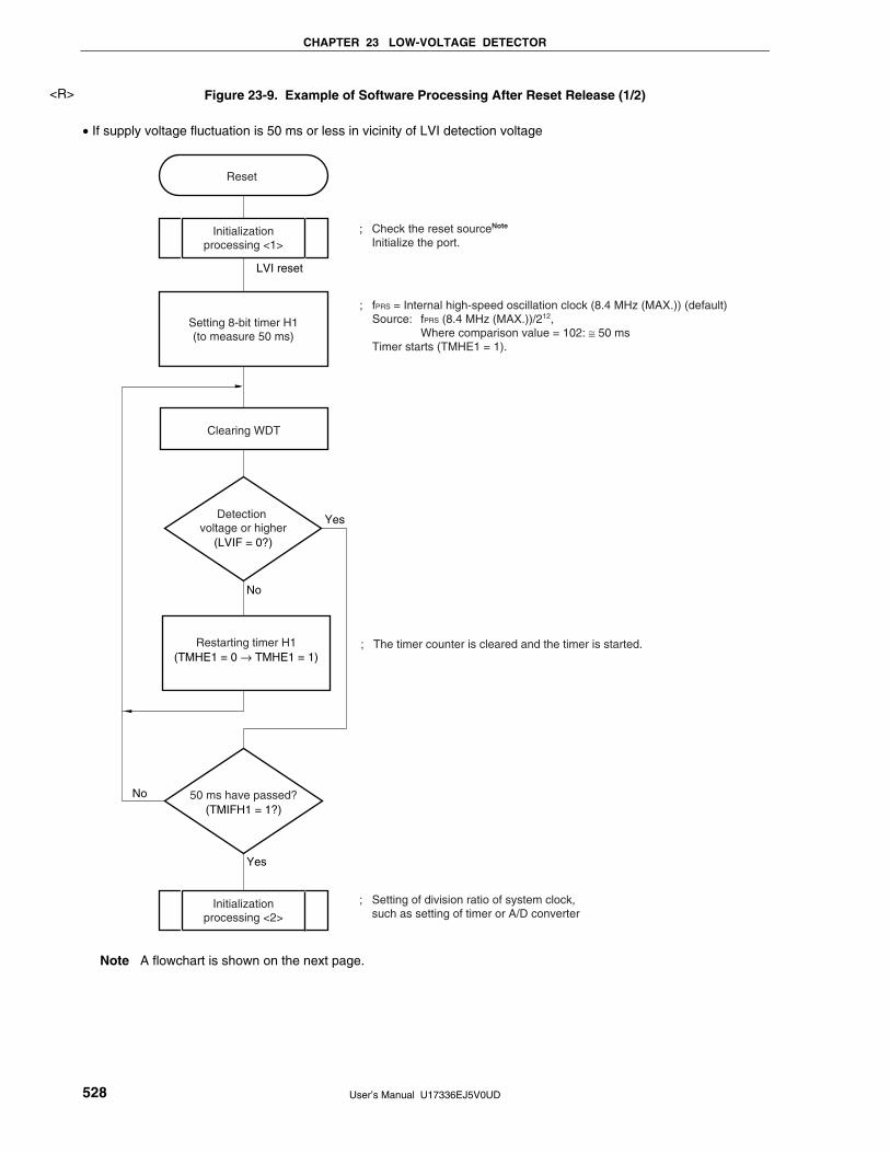
CHAPTER 23 LOW-VOLTAGE DETECTOR
User’s Manual U17336EJ5V0UD 528
Figure 23-9. Example of Software Processing After Reset Release (1/2)
• If supply voltage fluctuation is 50 ms or less in vicinity of LVI detection voltage
; Check the reset sourceNote
Initialize the port.
Reset
Initializationprocessing <1>
50 ms have passed?(TMIFH1 = 1?)
Initializationprocessing <2>
Setting 8-bit timer H1(to measure 50 ms)
; Setting of division ratio of system clock, such as setting of timer or A/D converter
Yes
No
Clearing WDT
Detection voltage or higher
(LVIF = 0?)
Yes
Restarting timer H1(TMHE1 = 0 → TMHE1 = 1)
No
; The timer counter is cleared and the timer is started.
LVI reset
; fPRS = Internal high-speed oscillation clock (8.4 MHz (MAX.)) (default)Source: fPRS (8.4 MHz (MAX.))/212,
Where comparison value = 102: ≅ 50 msTimer starts (TMHE1 = 1).
Note A flowchart is shown on the next page.
<R>

CHAPTER 23 LOW-VOLTAGE DETECTOR
User’s Manual U17336EJ5V0UD 529
Figure 23-9. Example of Software Processing After Reset Release (2/2)
• Checking reset source
Yes: Reset generation by LVI
No: Reset generation other than by LVI
Set LVI(Set LVIM and LVIS registers)
Check reset source
LVION of LVIMregister = 1?
<R>

User’s Manual U17336EJ5V0UD 530
CHAPTER 24 OPTION BYTE
24.1 Functions of Option Bytes
The flash memory at 0080H to 0084H of the 78K0/KC2 is an option byte area. When power is turned on or when
the device is restarted from the reset status, the device automatically references the option bytes and sets specified
functions. When using the product, be sure to set the following functions by using the option bytes.
When the boot swap operation is used during self programming, 0080H to 0084H are switched to 1080H to 1084H.
Therefore, set values that are the same as those of 0080H to 0084H to 1080H to 1084H in advance.
Caution Be sure to set 00H to 0082H and 0083H (0082H/1082H and 0083H/1083H when the boot swap
function is used).
(1) 0080H/1080H
Internal low-speed oscillator operation
• Can be stopped by software
• Cannot be stopped
Watchdog timer interval time setting
Watchdog timer counter operation
• Enabled counter operation
• Disabled counter operation
Watchdog timer window open period setting
Caution Set a value that is the same as that of 0080H to 1080H because 0080H and 1080H are
switched during the boot swap operation.
(2) 0081H/1081H
Selecting POC mode
• During 2.7 V/1.59 V POC mode operation (POCMODE = 1)
The device is in the reset state upon power application and until the supply voltage reaches 2.7 V (TYP.). It
is released from the reset state when the voltage exceeds 2.7 V (TYP.). After that, POC is not detected at
2.7 V but is detected at 1.59 V (TYP.).
With standard and (A) grade products, if the supply voltage rises to 1.8 V after power application at a rate
slower than 0.5 V/ms (MIN.), use of the 2.7 V/1.59 V POC mode is recommended.
• During 1.59 V POC mode operation (POCMODE = 0)
The device is in the reset state upon power application and until the supply voltage reaches 1.59 V (TYP.).
It is released from the reset state when the voltage exceeds 1.59 V (TYP.). After that, POC is detected at
1.59 V (TYP.), in the same manner as on power application.
Caution POCMODE can only be written by using a dedicated flash memory programmer. It cannot be
set during self programming or boot swap operation during self programming (at this time,
1.59 V POC mode (default) is set). However, because the value of 1081H is copied to 0081H
during the boot swap operation, it is recommended to set a value that is the same as that of
0081H to 1081H when the boot swap function is used.
<R>

CHAPTER 24 OPTION BYTE
User’s Manual U17336EJ5V0UD 531
(3) 0084H/1084H
On-chip debug operation control
• Disabling on-chip debug operation
• Enabling on-chip debug operation and erasing data of the flash memory in case authentication of the on-
chip debug security ID fails
• Enabling on-chip debug operation and not erasing data of the flash memory even in case authentication of
the on-chip debug security ID fails
Cautions 1. Be sure to set 00H (disabling on-chip debug operation) to 0084H for products not
equipped with the on-chip debug function (μPD78F0511, 78F0512, 78F0513, 78F0514, and
78F0515). Also set 00H to 1084H because 0084H and 1084H are switched during the boot
operation.
2. To use the on-chip debug function with a product equipped with the on-chip debug
function (μPD78F0513D, 78F0515D), set 02H or 03H to 0084H. Set a value that is the
same as that of 0084H to 1084H because 0084H and 1084H are switched during the boot
operation.

CHAPTER 24 OPTION BYTE
User’s Manual U17336EJ5V0UD 532
24.2 Format of Option Byte
The format of the option byte is shown below.
Figure 24-1. Format of Option Byte (1/2)
Address: 0080H/1080HNote
7 6 5 4 3 2 1 0
0 WINDOW1 WINDOW0 WDTON WDCS2 WDCS1 WDCS0 LSROSC
WINDOW1 WINDOW0 Watchdog timer window open period
0 0 25%
0 1 50%
1 0 75%
1 1 100%
WDTON Operation control of watchdog timer counter/illegal access detection
0 Counter operation disabled (counting stopped after reset), illegal access detection operation disabled
1 Counter operation enabled (counting started after reset), illegal access detection operation enabled
WDCS2 WDCS1 WDCS0 Watchdog timer overflow time
0 0 0 210/fRL (3.88 ms)
0 0 1 211/fRL (7.76 ms)
0 1 0 212/fRL (15.52 ms)
0 1 1 213/fRL (31.03 ms)
1 0 0 214/fRL (62.06 ms)
1 0 1 215/fRL (124.12 ms)
1 1 0 216/fRL (248.24 ms)
1 1 1 217/fRL (496.48 ms)
LSROSC Internal low-speed oscillator operation
0 Can be stopped by software (stopped when 1 is written to bit 1 (LSRSTOP) of RCM register)
1 Cannot be stopped (not stopped even if 1 is written to LSRSTOP bit)
Note Set a value that is the same as that of 0080H to 1080H because 0080H and 1080H are switched during the
boot swap operation.
Cautions 1. The combination of WDCS2 = WDCS1 = WDCS0 = 0 and WINDOW1 = WINDOW0 = 0 is prohibited.
2. The watchdog timer continues its operation during self programming and EEPROM emulation of the flash memory. During processing, the interrupt acknowledge time is delayed. Set the overflow time and window size taking this delay into consideration.
3. If LSROSC = 0 (oscillation can be stopped by software), the count clock is not supplied to the watchdog timer in the HALT and STOP modes, regardless of the setting of bit 1 (LSRSTOP) of the internal oscillation mode register (RCM).
When 8-bit timer H1 operates with the internal low-speed oscillation clock, the count clock is supplied to 8-bit timer H1 even in the HALT/STOP mode.
4. Be sure to clear bit 7 to 0.
Remarks 1. fRL: Internal low-speed oscillation clock frequency 2. ( ): fRL = 264 kHz (MAX.)
<R>

CHAPTER 24 OPTION BYTE
User’s Manual U17336EJ5V0UD 533
Figure 24-1. Format of Option Byte (2/2)
Address: 0081H/1081HNotes 1, 2
7 6 5 4 3 2 1 0
0 0 0 0 0 0 0 POCMODE
POCMODE POC mode selection
0 1.59 V POC mode (default)
1 2.7 V/1.59 V POC mode
Notes 1. POCMODE can only be written by using a dedicated flash memory programmer. It cannot be set
during self programming or boot swap operation during self programming (at this time, 1.59 V POC
mode (default) is set). However, because the value of 1081H is copied to 0081H during the boot swap
operation, it is recommended to set a value that is the same as that of 0081H to 1081H when the boot
swap function is used.
2. To change the setting for the POC mode, set the value to 0081H again after batch erasure (chip
erasure) of the flash memory. The setting cannot be changed after the memory of the specified block
is erased.
Caution Be sure to clear bits 7 to 1 to “0”.
Address: 0082H/1082H, 0083H/1083HNote
7 6 5 4 3 2 1 0
0 0 0 0 0 0 0 0
Note Be sure to set 00H to 0082H and 0083H, as these addresses are reserved areas. Also set 00H to 1082H
and 1083H because 0082H and 0083H are switched with 1082H and 1083H when the boot swap operation
is used.
Address: 0084H/1084HNotes 1, 2
7 6 5 4 3 2 1 0
0 0 0 0 0 0 OCDEN1 OCDEN0
OCDEN1 OCDEN0 On-chip debug operation control
0 0 Operation disabled
0 1 Setting prohibited
1 0 Operation enabled. Does not erase data of the flash memory in case authentication of the on-chip debug security ID fails.
1 1 Operation enabled. Erases data of the flash memory in case authentication of the on-chip debug security ID fails.
Notes 1. Be sure to set 00H (on-chip debug operation disabled) to 0084H for products not equipped with the on-
chip debug function (μPD78F0511, 78F0512, 78F0513, 78F0514, and 78F0515). Also set 00H to
1084H because 0084H and 1084H are switched during the boot swap operation.
2. To use the on-chip debug function with a product equipped with the on-chip debug function
(μPD78F0513D, 78F0515D), set 02H or 03H to 0084H. Set a value that is the same as that of 0084H
to 1084H because 0084H and 1084H are switched during the boot swap operation.
Remark For the on-chip debug security ID, see CHAPTER 26 ON-CHIP DEBUG FUNCTION (μPD78F0513D
AND 78F0515D ONLY).

CHAPTER 24 OPTION BYTE
User’s Manual U17336EJ5V0UD 534
Here is an example of description of the software for setting the option bytes.
OPT CSEG AT 0080H
OPTION: DB 30H ; Enables watchdog timer operation (illegal access detection operation),
; Window open period of watchdog timer: 50%,
; Overflow time of watchdog timer: 210/fRL,
; Internal low-speed oscillator can be stopped by software.
DB 00H ; 1.59 V POC mode
DB 00H ; Reserved area
DB 00H ; Reserved area
DB 00H ; On-chip debug operation disabled
Remark Referencing of the option byte is performed during reset processing. For the reset processing timing,
see CHAPTER 21 RESET FUNCTION.
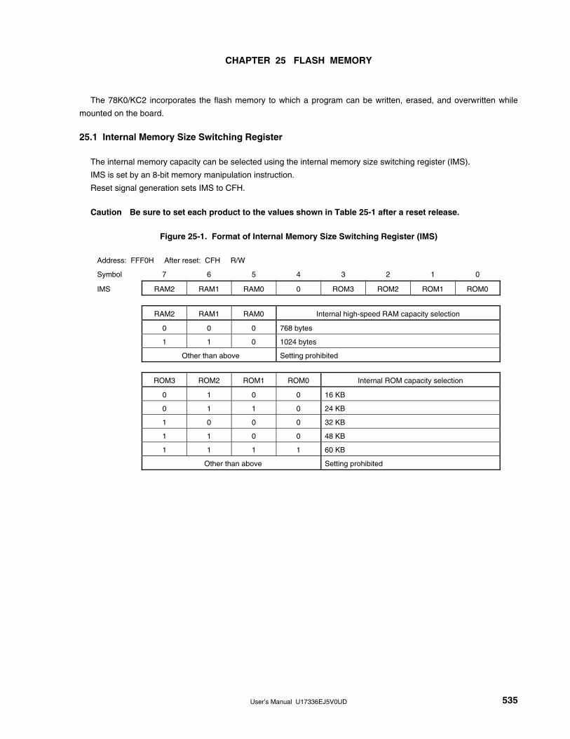
User’s Manual U17336EJ5V0UD 535
CHAPTER 25 FLASH MEMORY
The 78K0/KC2 incorporates the flash memory to which a program can be written, erased, and overwritten while
mounted on the board.
25.1 Internal Memory Size Switching Register
The internal memory capacity can be selected using the internal memory size switching register (IMS).
IMS is set by an 8-bit memory manipulation instruction.
Reset signal generation sets IMS to CFH.
Caution Be sure to set each product to the values shown in Table 25-1 after a reset release.
Figure 25-1. Format of Internal Memory Size Switching Register (IMS)
Address: FFF0H After reset: CFH R/W
Symbol 7 6 5 4 3 2 1 0
IMS RAM2 RAM1 RAM0 0 ROM3 ROM2 ROM1 ROM0
RAM2 RAM1 RAM0 Internal high-speed RAM capacity selection
0 0 0 768 bytes
1 1 0 1024 bytes
Other than above Setting prohibited
ROM3 ROM2 ROM1 ROM0 Internal ROM capacity selection
0 1 0 0 16 KB
0 1 1 0 24 KB
1 0 0 0 32 KB
1 1 0 0 48 KB
1 1 1 1 60 KB
Other than above Setting prohibited

CHAPTER 25 FLASH MEMORY
User’s Manual U17336EJ5V0UD 536
Table 25-1. Internal Memory Size Switching Register Settings
Flash Memory Versions (78K0/KC2) IMS Setting
μPD78F0511 04H
μPD78F0512 C6H
μPD78F0513, 78F0513DNote C8H
μPD78F0514 CCH
μPD78F0515, 78F0515DNote CFH
Note The internal ROM and internal high-speed RAM capacities of the products with the on-chip debug function
can be debugged by setting IMS, according to the debug target products. Set IMS according to the debug
target products.
25.2 Internal Expansion RAM Size Switching Register
The internal expansion RAM capacity can be selected using the internal expansion RAM size switching register
(IXS).
IXS is set by an 8-bit memory manipulation instruction.
Reset signal generation sets IXS to 0CH.
Caution Be sure to set each product to the values shown in Table 25-2 after a reset release.
Figure 25-2. Format of Internal Expansion RAM Size Switching Register (IXS)
Address: FFF4H After reset: 0CH R/W
Symbol 7 6 5 4 3 2 1 0
IXS 0 0 0 IXRAM4 IXRAM3 IXRAM2 IXRAM1 IXRAM0
IXRAM4 IXRAM3 IXRAM2 IXRAM1 IXRAM0 Internal expansion RAM capacity selection
0 1 1 0 0 0 byte
0 1 0 1 0 1024 bytes
0 1 0 0 0 2048 bytes
Other than above Setting prohibited
Table 25-2. Internal Expansion RAM Size Switching Register Settings
Flash Memory Versions (78K0/KC2) IXS Setting
μPD78F0511
μPD78F0512
μPD78F0513, 78F0513DNote
0CH
μPD78F0514 0AH
μPD78F0515, 78F0515DNote 08H
Note The internal expansion RAM capacity of the products with the on-chip debug function can be debugged by
setting IXS, according to the debug target products. Set IXS according to the debug target products.
<R>
<R>

CHAPTER 25 FLASH MEMORY
User’s Manual U17336EJ5V0UD 537
25.3 Writing with Flash Memory Programmer
Data can be written to the flash memory on-board or off-board, by using a dedicated flash memory programmer.
(1) On-board programming
The contents of the flash memory can be rewritten after the 78K0/KC2 has been mounted on the target system.
The connectors that connect the dedicated flash memory programmer must be mounted on the target system.
(2) Off-board programming
Data can be written to the flash memory with a dedicated program adapter (FA series) before the 78K0/KC2 is
mounted on the target system.
Remark The FA series is a product of Naito Densei Machida Mfg. Co., Ltd.
Table 25-3. Wiring Between 78K0/KC2 and Dedicated Flash Memory Programmer (1/2)
(a) 38-pin products
Pin Configuration of Dedicated Flash Memory Programmer With CSI10 With UART6
Signal Name I/O Pin Function Pin Name Pin No. Pin Name Pin No.
SI/RxD Input Receive signal SO10/P12 30 TxD6/P13 29
SO/TxD Output Transmit signal SI10/RxD0/P11 31 RxD6/P14 28
SCK Output Transfer clock SCK10/TxD0/P10 32 − −
CLK Output Clock to 78K0/KC2 −Note 1 − Note 2 Note 2
/RESET Output Reset signal RESET 6 RESET 6
FLMD0 Output Mode signal FLMD0 9 FLMD0 9
VDD 14 VDD 14 VDD I/O VDD voltage generation/
power monitoring AVREF 33 AVREF 33
VSS 13 VSS 13 GND − Ground
AVSS 34 AVSS 34
Notes 1. Only the internal high-speed oscillation clock (fRH) can be used when CSI10 is used.
2. Only the X1 clock (fX) or external main system clock (fEXCLK) can be used when UART6 is used. When
using the clock output of the dedicated flash memory programmer, pin connection varies depending on the
type of the dedicated flash memory programmer used.
• PG-FP4, FL-PR4: Connect CLK of the programmer to EXCLK/X2/P122 (pin 10).
• PG-FPL3, FP-LITE3: Connect CLK of the programmer to X1/P121 (pin 11), and connect its inverted
signal to X2/EXCLK/P122 (pin 10).
<R>

CHAPTER 25 FLASH MEMORY
User’s Manual U17336EJ5V0UD 538
Table 25-3. Wiring Between 78K0/KC2 and Dedicated Flash Memory Programmer (2/2)
(b) 44-pin products
Pin Configuration of Dedicated Flash Memory Programmer With CSI10 With UART6
Signal Name I/O Pin Function Pin Name Pin No. Pin Name Pin No.
SI/RxD Input Receive signal SO10/P12 29 TxD6/P13 28
SO/TxD Output Transmit signal SI10/RxD0/P11 30 RxD6/P14 27
SCK Output Transfer clock SCK10/TxD0/P10 31 − −
CLK Output Clock to 78K0/KC2 −Note 1 − Note 2 Note 2
/RESET Output Reset signal RESET 3 RESET 3
FLMD0 Output Mode signal FLMD0 6 FLMD0 6
VDD 11 VDD 11 VDD I/O VDD voltage generation/
power monitoring AVREF 32 AVREF 32
VSS 10 VSS 10 GND − Ground
AVSS 33 AVSS 33
Notes 1. Only the internal high-speed oscillation clock (fRH) can be used when CSI10 is used.
2. Only the X1 clock (fX) or external main system clock (fEXCLK) can be used when UART6 is used. When
using the clock output of the dedicated flash memory programmer, pin connection varies depending on the
type of the dedicated flash memory programmer used.
• PG-FP4, FL-PR4: Connect CLK of the programmer to EXCLK/X2/P122 (pin 7).
• PG-FPL3, FP-LITE3: Connect CLK of the programmer to X1/P121 (pin 8), and connect its inverted
signal to X2/EXCLK/P122 (pin 7).
(c) 48-pin products
Pin Configuration of Dedicated Flash Memory Programmer With CSI10 With UART6
Signal Name I/O Pin Function Pin Name Pin No. Pin Name Pin No.
SI/RxD Input Receive signal SO10/P12 20 TxD6/P13 19
SO/TxD Output Transmit signal SI10/RxD0/P11 21 RxD6/P14 18
SCK Output Transfer clock SCK10/TxD0/P10 22 − −
CLK Output Clock to 78K0/KC2 −Note 1 − Note 2 Note 2
/RESET Output Reset signal RESET 40 RESET 40
FLMD0 Output Mode signal FLMD0 43 FLMD0 43
VDD 48 VDD 48 VDD I/O VDD voltage generation/
power monitoring AVREF 23 AVREF 23
VSS 47 VSS 47 GND − Ground
AVSS 24 AVSS 24
Notes 1. Only the internal high-speed oscillation clock (fRH) can be used when CSI10 is used.
2. Only the X1 clock (fX) or external main system clock (fEXCLK) can be used when UART6 is used. When
using the clock output of the dedicated flash memory programmer, pin connection varies depending on the
type of the dedicated flash memory programmer used.
• PG-FP4, FL-PR4: Connect CLK of the programmer to EXCLK/X2/P122 (pin 44).
• PG-FPL3, FP-LITE3: Connect CLK of the programmer to X1/P121 (pin 45), and connect its inverted
signal to X2/EXCLK/P122 (pin 44).

CHAPTER 25 FLASH MEMORY
User’s Manual U17336EJ5V0UD 539
Examples of the recommended connection when using the adapter for flash memory writing are shown below.
Figure 25-3. Example of Wiring Adapter for Flash Memory Writing in 3-Wire Serial I/O (CSI10) Mode
(38-Pin Products)
1
2
3
4
5
6
7
8
9
10
11
12
13
14
15
16
17
18
19
38
37
36
35
34
33
32
31
30
29
28
27
26
25
24
23
22
21
20
GND
VDD
VDD2
SI SO SCK CLK /RESET
WRITER INTERFACE
FLMD0
GND
VDD (2.7 to 5.5 V)
<R>

CHAPTER 25 FLASH MEMORY
User’s Manual U17336EJ5V0UD 540
Figure 25-4. Example of Wiring Adapter for Flash Memory Writing in UART (UART6) Mode
(38-Pin Products)
1
2
3
4
5
6
7
8
9
10Note
11
12
13
14
15
16
17
18
19
38
37
36
35
34
33
32
31
30
29
28
27
26
25
24
23
22
21
20
GND
VDD
VDD2
SI SO SCK CLKNote /RESET
WRITER INTERFACE
FLMD0
GND
VDD (2.7 to 5.5 V)
Note The above figure illustrates an example of wiring when using the clock output from the PG-FP4 or FL-PR4.
When using the clock output from the PG-FPL3 or FP-LITE3, connect CLK to X1/P121 (pin 11), and connect
its inverted signal to X2/EXCLK/P122 (pin 10).
<R>

CHAPTER 25 FLASH MEMORY
User’s Manual U17336EJ5V0UD 541
Figure 25-5. Example of Wiring Adapter for Flash Memory Writing in 3-Wire Serial I/O (CSI10) Mode
(44-Pin Products)
44 43 42 41 40 39 38
1312 14 15 16 17 18 19 20 21 2223
1
2
3
4
5
6
7
8
91011
36 35 3433
32
31
30
29
28
27
2625
37
24
GNDVDDVDD2
SI SO SCK CLK /RESET
WRITER INTERFACE
VDD (2.7 to 5.5 V)
GND
FLMD0
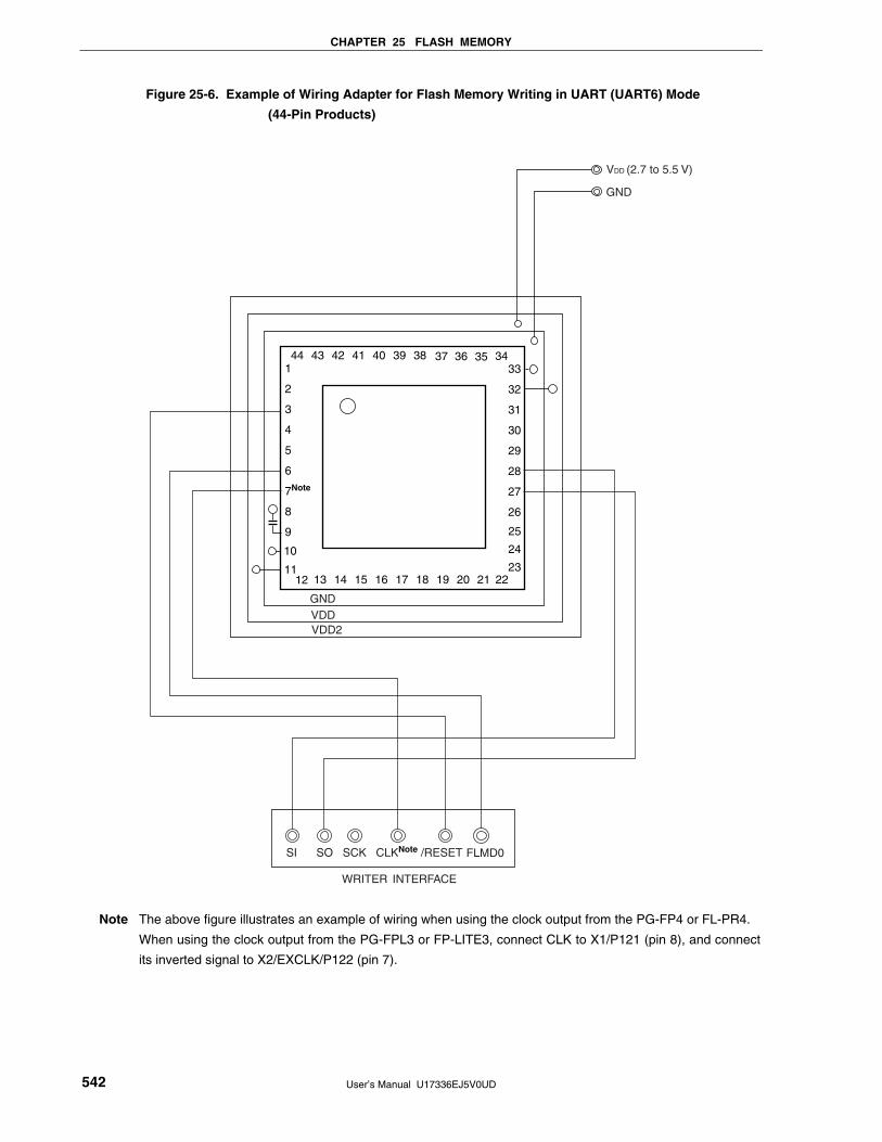
CHAPTER 25 FLASH MEMORY
User’s Manual U17336EJ5V0UD 542
Figure 25-6. Example of Wiring Adapter for Flash Memory Writing in UART (UART6) Mode
(44-Pin Products)
44 43 42 41 40 39 38
1312 14 15 16 17 18 19 20 21 2223
1
2
3
4
5
6
7Note
8
9
10
11
36 35 3433
32
31
30
29
28
27
26
25
37
24
GNDVDDVDD2
SI SO SCK CLKNote /RESET
WRITER INTERFACE
VDD (2.7 to 5.5 V)
GND
FLMD0
Note The above figure illustrates an example of wiring when using the clock output from the PG-FP4 or FL-PR4.
When using the clock output from the PG-FPL3 or FP-LITE3, connect CLK to X1/P121 (pin 8), and connect
its inverted signal to X2/EXCLK/P122 (pin 7).

CHAPTER 25 FLASH MEMORY
User’s Manual U17336EJ5V0UD 543
Figure 25-7. Example of Wiring Adapter for Flash Memory Writing in 3-Wire Serial I/O (CSI10) Mode
(48-Pin Products)
48 47 46 45 44 43 42 41 40 39 38
13 14 15 16 17 18 19 20 21 22 23
1
2
3
4
5
6
7
8
9
10
11
36
35
34
33
32
31
30
29
28
27
2612 25
37
24GNDVDDVDD2
SI SO SCK CLK /RESET FLMD0
WRITER INTERFACE
VDD (2.7 to 5.5 V)
GND

CHAPTER 25 FLASH MEMORY
User’s Manual U17336EJ5V0UD 544
Figure 25-8. Example of Wiring Adapter for Flash Memory Writing in UART (UART6) Mode
(48-Pin Products)
48 47 46 45 44Note
43 42 41 40 39 38
13 14 15 16 17 18 19 20 21 22 23
1
2
3
4
5
6
7
8
9
10
11
36
35
34
33
32
31
30
29
28
27
26
12 25
37
24
GND
VDDVDD2
SI SO SCK CLKNote /RESET FLMD0
WRITER INTERFACE
VDD (2.7 to 5.5 V)
GND
Note The above figure illustrates an example of wiring when using the clock output from the PG-FP4 or FL-PR4.
When using the clock output from the PG-FPL3 or FP-LITE3, connect CLK to X1/P121 (pin 45), and connect
its inverted signal to X2/EXCLK/P122 (pin 44).

CHAPTER 25 FLASH MEMORY
User’s Manual U17336EJ5V0UD 545
25.4 Programming Environment
The environment required for writing a program to the flash memory of the 78K0/KC2 is illustrated below.
Figure 25-9. Environment for Writing Program to Flash Memory
RS-232C
USB
78K0/KC2
FLMD0
VDD
VSS
RESET
CSI10/UART6
Host machine


CHAPTER 25 FLASH MEMORY
User’s Manual U17336EJ5V0UD 547
25.6 Handling of Pins on Board
To write the flash memory on-board, connectors that connect the dedicated flash memory programmer must be
provided on the target system. First provide a function that selects the normal operation mode or flash memory
programming mode on the board.
When the flash memory programming mode is set, all the pins not used for programming the flash memory are in
the same status as immediately after reset. Therefore, if the external device does not recognize the state immediately
after reset, the pins must be handled as described below.
25.6.1 FLMD0 pin
In the normal operation mode, 0 V is input to the FLMD0 pin. In the flash memory programming mode, the VDD
write voltage is supplied to the FLMD0 pin. An FLMD0 pin connection example is shown below.
Figure 25-12. FLMD0 Pin Connection Example
78K0/KC2
FLMD0
10 kΩ (recommended)
Dedicated flash memory programmer connection pin
25.6.2 Serial interface pins
The pins used by each serial interface are listed below.
Table 25-5. Pins Used by Each Serial Interface
Serial Interface Pins Used
CSI10 SO10, SI10, SCK10
UART6 TxD6, RxD6
To connect the dedicated flash memory programmer to the pins of a serial interface that is connected to another
device on the board, care must be exercised so that signals do not collide or that the other device does not
malfunction.
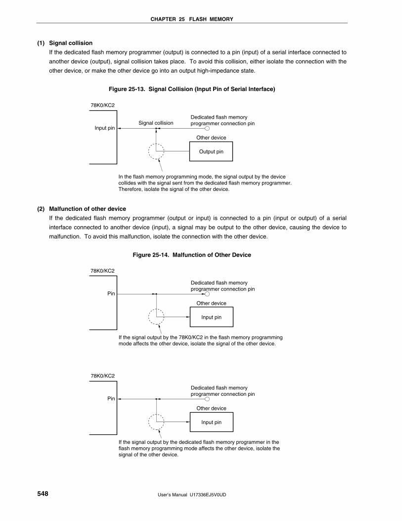
CHAPTER 25 FLASH MEMORY
User’s Manual U17336EJ5V0UD 548
(1) Signal collision
If the dedicated flash memory programmer (output) is connected to a pin (input) of a serial interface connected to
another device (output), signal collision takes place. To avoid this collision, either isolate the connection with the
other device, or make the other device go into an output high-impedance state.
Figure 25-13. Signal Collision (Input Pin of Serial Interface)
Input pinSignal collision
Dedicated flash memory programmer connection pin
Other device
Output pin
In the flash memory programming mode, the signal output by the device collides with the signal sent from the dedicated flash memory programmer. Therefore, isolate the signal of the other device.
78K0/KC2
(2) Malfunction of other device
If the dedicated flash memory programmer (output or input) is connected to a pin (input or output) of a serial
interface connected to another device (input), a signal may be output to the other device, causing the device to
malfunction. To avoid this malfunction, isolate the connection with the other device.
Figure 25-14. Malfunction of Other Device
Pin
Dedicated flash memory programmer connection pin
Other device
Input pin
If the signal output by the 78K0/KC2 in the flash memory programming mode affects the other device, isolate the signal of the other device.
Pin
Dedicated flash memory programmer connection pin
Other device
Input pin
If the signal output by the dedicated flash memory programmer in the flash memory programming mode affects the other device, isolate the signal of the other device.
78K0/KC2
78K0/KC2

CHAPTER 25 FLASH MEMORY
User’s Manual U17336EJ5V0UD 549
25.6.3 RESET pin
If the reset signal of the dedicated flash memory programmer is connected to the RESET pin that is connected to
the reset signal generator on the board, signal collision takes place. To prevent this collision, isolate the connection
with the reset signal generator.
If the reset signal is input from the user system while the flash memory programming mode is set, the flash
memory will not be correctly programmed. Do not input any signal other than the reset signal of the dedicated flash
memory programmer.
Figure 25-15. Signal Collision (RESET Pin)
RESET
Dedicated flash memory programmer connection signal
Reset signal generator
Signal collision
Output pin
In the flash memory programming mode, the signal output by the reset signal generator collides with the signal output by the dedicated flash memory programmer. Therefore, isolate the signal of the reset signal generator.
78K0/KC2
25.6.4 Port pins
When the flash memory programming mode is set, all the pins not used for flash memory programming enter the
same status as that immediately after reset. If external devices connected to the ports do not recognize the port
status immediately after reset, the port pin must be connected to VDD or VSS via a resistor.
25.6.5 REGC pin
Connect the REGC pin to GND via a capacitor (0.47 to 1 μF: recommended) in the same manner as during normal
operation.
25.6.6 Other signal pins
Connect X1 and X2 in the same status as in the normal operation mode when using the on-board clock.
To input the operating clock from the dedicated flash memory programmer, however, connect as follows.
• PG-FP4, FL-PR4: Connect CLK of the programmer to EXCLK/X2/P122.
• PG-FPL3, FP-LITE3: Connect CLK of the programmer and X1/P121, and connect its inverted signal to
X2/EXCLK/P122.
Cautions 1. Only the internal high-speed oscillation clock (fRH) can be used when CSI10 is used.
2. Only the X1 clock (fX) or external main system clock (fEXCLK) can be used when UART6 is used.

CHAPTER 25 FLASH MEMORY
User’s Manual U17336EJ5V0UD 550
Caution 3. For products without an on-chip debug function, with the flash memory of 48 KB or more
(μPD78F0514 and 78F0515), and having a product rank of “I”, “K”, or “E”, and for the product
with an on-chip debug function (μPD78F0513D and 78F0515D), connect P31/INTP2/OCD1ANote
and P121/X1/OCD0ANote as follows when writing the flash memory with a flash memory
programmer.
• P31/INTP2/OCD1ANote: Connect to VSS via a resistor (10 kΩ: recommended).
• P121/X1/OCD0ANote: When using this pin as a port, connect it to VSS via a resistor (10 kΩ:
recommended) (in the input mode) or leave it open (in the output
mode).
The above connection is not necessary when writing the flash memory by means of self
programming.
Note OCD0A and OCD1A are provided to the μPD78F0513D and 78F0515D only.
Remark For the product ranks, consult an NEC Electronics sales representative.
25.6.7 Power supply
To use the supply voltage output of the flash memory programmer, connect the VDD pin to VDD of the flash memory
programmer, and the VSS pin to GND of the flash memory programmer.
To use the on-board supply voltage, connect in compliance with the normal operation mode.
However, be sure to connect the VDD and VSS pins to VDD and GND of the flash memory programmer to use the
power monitor function with the flash memory programmer, even when using the on-board supply voltage.
Supply the same other power supplies (AVREF and AVSS) as those in the normal operation mode.
<R>

CHAPTER 25 FLASH MEMORY
User’s Manual U17336EJ5V0UD 551
25.7 Programming Method
25.7.1 Controlling flash memory
The following figure illustrates the procedure to manipulate the flash memory.
Figure 25-16. Flash Memory Manipulation Procedure
Start
Selecting communication mode
Manipulate flash memory
End?
Yes
FLMD0 pulse supply
No
End
Flash memory programming mode is set
25.7.2 Flash memory programming mode
To rewrite the contents of the flash memory by using the dedicated flash memory programmer, set the 78K0/KC2
in the flash memory programming mode. To set the mode, set the FLMD0 pin to VDD and clear the reset signal.
Change the mode by using a jumper when writing the flash memory on-board.
Figure 25-17. Flash Memory Programming Mode
VDD
RESET
5.5 V
0 V
VDD
0 V
Flash memory programming mode
FLMD0
FLMD0 pulse
VDD
0 V
Table 25-6. Relationship Between FLMD0 Pin and Operation Mode After Reset Release
FLMD0 Operation Mode
0 Normal operation mode
VDD Flash memory programming mode

CHAPTER 25 FLASH MEMORY
User’s Manual U17336EJ5V0UD 552
25.7.3 Selecting communication mode
In the 78K0/KC2, a communication mode is selected by inputting pulses to the FLMD0 pin after the dedicated flash
memory programming mode is entered. These FLMD0 pulses are generated by the flash memory programmer.
The following table shows the relationship between the number of pulses and communication modes.
Table 25-7. Communication Modes
Standard SettingNote 1 Communication Mode Port Speed Frequency Multiply Rate
Pins Used Peripheral Clock
Number of FLMD0 Pulses
UART-Ext-Osc fX 0 UART (UART6) UART-Ext-FP4CK
115,200 bpsNote 3 2 to 20 MHzNote 2 TxD6, RxD6
fEXCLK 3
3-wire serial I/O (CSI10)
CSI-Internal-OSC 2.4 kHz to 2.5 MHz
−
1.0
SO10, SI10, SCK10
fRH 8
Notes 1. Selection items for Standard settings on GUI of the flash memory programmer.
2. The possible setting range differs depending on the voltage. For details, refer to the chapter of electrical
specifications.
3. Because factors other than the baud rate error, such as the signal waveform slew, also affect UART
communication, thoroughly evaluate the slew as well as the baud rate error.
Caution When UART6 is selected, the receive clock is calculated based on the reset command sent from the
dedicated flash memory programmer after the FLMD0 pulse has been received.
Remark fX: X1 clock
fEXCLK: External main system clock
fRH: Internal high-speed oscillation clock

CHAPTER 25 FLASH MEMORY
User’s Manual U17336EJ5V0UD 553
25.7.4 Communication commands
The 78K0/KC2 communicates with the dedicated flash memory programmer by using commands. The signals sent
from the flash memory programmer to the 78K0/KC2 are called commands, and the signals sent from the 78K0/KC2
to the dedicated flash memory programmer are called response.
Figure 25-18. Communication Commands
Command
Response
78K0/KC2Dedicated flashprogrammer
PG-FP4 (Flash Pro4)
Cxxxxxx
Bxxxxx
Axxxx
XX
X Y
YY
XX
XX
XX
XX
XX
XX
XX
X
XX
XX
YY
YY
STATVE
The flash memory control commands of the 78K0/KC2 are listed in the table below. All these commands are
issued from the programmer and the 78K0/KC2 performs processing corresponding to the respective commands.
Table 25-8. Flash Memory Control Commands
Classification Command Name Function
Verify Verify Compares the contents of a specified area of the flash memory with
data transmitted from the programmer.
Chip Erase Erases the entire flash memory. Erase
Block Erase Erases a specified area in the flash memory.
Blank check Block Blank Check Checks if a specified block in the flash memory has been correctly
erased.
Write Programming Writes data to a specified area in the flash memory.
Status Gets the current operating status (status data).
Silicon Signature Gets 78K0/Kx2 information (such as the part number and flash memory
configuration).
Version Get Gets the 78K0/Kx2 version and firmware version.
Getting information
Checksum Gets the checksum data for a specified area.
Security Security Set Sets security information.
Reset Used to detect synchronization status of communication. Others
Oscillating Frequency Set Specifies an oscillation frequency.
The 78K0/KC2 returns a response for the command issued by the dedicated flash memory programmer. The
response names sent from the 78K0/KC2 are listed below.
Table 25-9. Response Names
Response Name Function
ACK Acknowledges command/data.
NAK Acknowledges illegal command/data.
CHAPTER 25 FLASH MEMORY
User’s Manual U17336EJ5V0UD 554
25.8 Security Settings
The 78K0/KC2 supports a security function that prohibits rewriting the user program written to the internal flash
memory, so that the program cannot be changed by an unauthorized person.
The operations shown below can be performed using the security set command. The security setting is valid when
the programming mode is set next.
• Disabling batch erase (chip erase)
Execution of the block erase and batch erase (chip erase) commands for entire blocks in the flash memory is
prohibited by this setting during on-board/off-board programming. Once execution of the batch erase (chip
erase) command is prohibited, all of the prohibition settings (including prohibition of batch erase (chip erase)) can
no longer be cancelled.
Caution After the security setting for the batch erase is set, erasure cannot be performed for the device.
In addition, even if a write command is executed, data different from that which has already
been written to the flash memory cannot be written, because the erase command is disabled.
• Disabling block erase
Execution of the block erase command for a specific block in the flash memory is prohibited during on-board/off-
board programming. However, blocks can be erased by means of self programming.
• Disabling write
Execution of the write and block erase commands for entire blocks in the flash memory is prohibited during on-
board/off-board programming. However, blocks can be written by means of self programming.
• Disabling rewriting boot cluster 0
Execution of the batch erase (chip erase) command, block erase command, and write command on boot cluster
0 (0000H to 0FFFH) in the flash memory is prohibited by this setting.
Caution If a security setting that rewrites boot cluster 0 has been applied, boot cluster 0 of that device
will not be rewritten.
The batch erase (chip erase), block erase, write commands, and rewriting boot cluster 0 are enabled by the default
setting when the flash memory is shipped. Security can be set by on-board/off-board programming and self
programming. Each security setting can be used in combination.
Prohibition of erasing blocks and writing is cleared by executing the batch erase (chip erase) command.
Table 25-10 shows the relationship between the erase and write commands when the 78K0/KC2 security function
is enabled.

CHAPTER 25 FLASH MEMORY
User’s Manual U17336EJ5V0UD 555
Table 25-10. Relationship Between Enabling Security Function and Command
(1) During on-board/off-board programming
Executed Command Valid Security
Batch Erase (Chip Erase) Block Erase Write
Prohibition of batch erase (chip erase) Cannot be erased in batch Can be performedNote.
Prohibition of block erase Can be performed.
Prohibition of writing
Can be erased in batch.
Blocks cannot be
erased.
Cannot be performed.
Prohibition of rewriting boot cluster 0 Cannot be erased in batch Boot cluster 0 cannot be
erased.
Boot cluster 0 cannot be
written.
Note Confirm that no data has been written to the write area. Because data cannot be erased after batch erase
(chip erase) is prohibited, do not write data if the data has not been erased.
(2) During self programming
Executed Command Valid Security
Block Erase Write
Prohibition of batch erase (chip erase)
Prohibition of block erase
Prohibition of writing
Blocks can be erased. Can be performed.
Prohibition of rewriting boot cluster 0 Boot cluster 0 cannot be erased. Boot cluster 0 cannot be written.
Table 25-11 shows how to perform security settings in each programming mode.
Table 25-11. Setting Security in Each Programming Mode
(1) On-board/off-board programming
Security Security Setting How to Disable Security Setting
Prohibition of batch erase (chip erase) Cannot be disabled after set.
Prohibition of block erase
Prohibition of writing
Execute batch erase (chip erase)
command
Prohibition of rewriting boot cluster 0
Set via GUI of dedicated flash memory
programmer, etc.
Cannot be disabled after set.
(2) Self programming
Security Security Setting How to Disable Security Setting
Prohibition of batch erase (chip erase) Cannot be disabled after set.
Prohibition of block erase
Prohibition of writing
Execute batch erase (chip erase)
command during on-board/off-board
programming (cannot be disabled during
self programming)
Prohibition of rewriting boot cluster 0
Set by using information library.
Cannot be disabled after set.

CHAPTER 25 FLASH MEMORY
User’s Manual U17336EJ5V0UD 556
25.9 Processing Time for Each Command When PG-FP4 Is Used (Reference)
The following table shows the processing time for each command (reference) when the PG-FP4 is used as a
dedicated flash memory programmer.
Table 25-12. Processing Time for Each Command When PG-FP4 Is Used (Reference)
(1) μPD78F0515, 78F0515D (internal ROM capacity: 60 KB)
Port: UART-Ext-FP4CK (External main system clock (fEXCLK)),
Speed: 115,200 bps
Command of
PG-FP4
Port: CSI-Internal-OSC
(Internal high-speed
oscillation clock (fRH)),
Speed: 2.5 MHz Frequency: 2.0 MHz Frequency: 20 MHz
Signature 0.5 s (TYP.) 0.5 s (TYP.) 0.5 s (TYP.)
Blankcheck 1 s (TYP.) 1 s (TYP.) 1 s (TYP.)
Erase 1.5 s (TYP.) 1 s (TYP.) 1 s (TYP.)
Program 5 s (TYP.) 9 s (TYP.) 9 s (TYP.)
Verify 2 s (TYP.) 6.5 s (TYP.) 6.5 s (TYP.)
E.P.V 6 s (TYP.) 10.5 s (TYP.) 10.5 s (TYP.)
Checksum 0.5 s (TYP.) 1 s (TYP.) 1 s (TYP.)
Security 0.5 s (TYP.) 0.5 s (TYP.) 0.5 s (TYP.)
(2) μPD78F0513, 78F0513D (internal ROM capacity: 32 KB)
Port: UART-Ext-FP4CK (External main system clock (fEXCLK)),
Speed: 115,200 bps
Command of
PG-FP4
Port: CSI-Internal-OSC
(Internal high-speed
oscillation clock (fRH)),
Speed: 2.5 MHz Frequency: 2.0 MHz Frequency: 20 MHz
Signature 0.5 s (TYP.) 0.5 s (TYP.) 0.5 s (TYP.)
Blankcheck 0.5 s (TYP.) 0.5 s (TYP.) 0.5 s (TYP.)
Erase 0.5 s (TYP.) 0.5 s (TYP.) 0.5 s (TYP.)
Program 2.5 s (TYP.) 5 s (TYP.) 5 s (TYP.)
Verify 1.5 s (TYP.) 4 s (TYP.) 3.5 s (TYP.)
E.P.V 3.5 s (TYP.) 6 s (TYP.) 6 s (TYP.)
Checksum 0.5 s (TYP.) 0.5 s (TYP.) 0.5 s (TYP.)
Security 0.5 s (TYP.) 0.5 s (TYP.) 0.5 s (TYP.)
Caution When executing boot swapping, do not use the E.P.V. command with the dedicated flash
memory programmer.
<R>

CHAPTER 25 FLASH MEMORY
User’s Manual U17336EJ5V0UD 557
25.10 Flash Memory Programming by Self Programming
The 78K0/KC2 supports a self programming function that can be used to rewrite the flash memory via a user
program. Because this function allows a user application to rewrite the flash memory by using a self programming
library, it can be used to upgrade the program in the field.
If an interrupt occurs during self programming, self programming can be temporarily stopped and interrupt servicing
can be executed. To execute interrupt servicing, restore the normal operation mode after self programming has been
stopped, and execute the EI instruction. After the self programming mode is later restored, self programming can be
resumed.
Remark For details of the self programming function and the 78K0/KC2 self programming library, refer to
78K0/Kx2 Flash Memory Self Programming User’s Manual (U17516E).
Cautions 1. The self programming function cannot be used when the CPU operates with the subsystem
clock.
2. Input a high level to the FLMD0 pin during self programming.
3. Be sure to execute the DI instruction before starting self programming.
The self programming function checks the interrupt request flags (IF0L, IF0H, IF1L, and IF1H).
If an interrupt request is generated, self programming is stopped.
4. Self programming is also stopped by an interrupt request that is not masked even in the DI
status. To prevent this, mask the interrupt by using the interrupt mask flag registers (MK0L,
MK0H, MK1L, and MK1H).
5. Allocate the entry program for self programming in the common area of 0000H to 7FFFH.
Figure 25-19. Operation Mode and Memory Map for Self Programming (μPD78F0515)
Normal mode
Flash memory(common area)
0 0 0 0 H
8 0 0 0 H7 F F F H
F F F F H
F B 0 0 HF A F F H
F 0 0 0 HE F F F H
F 8 0 0 HF 7 F F H
F F 0 0 HF E F F H
Internal high-speed RAM
Internalexpansion RAM
SFR
Flash memorycontrol
firmware ROM
Disableaccessing
Self programming mode
Flash memory(common area)
0 0 0 0 H
8 0 0 0 H7 F F F H
F F F F H
F B 0 0 HF A F F H
F 0 0 0 HE F F F H
F 8 0 0 HF 7 F F H
F F 0 0 HF E F F H
Internal high-speed RAM
Internalexpansion RAM
SFR
ReservedReserved
Flash memorycontrol
firmware ROM
Disableaccessing
Enableaccessing
Instructions can be fetched from common area .
Instructions can be fetched from common area and firmware ROM.
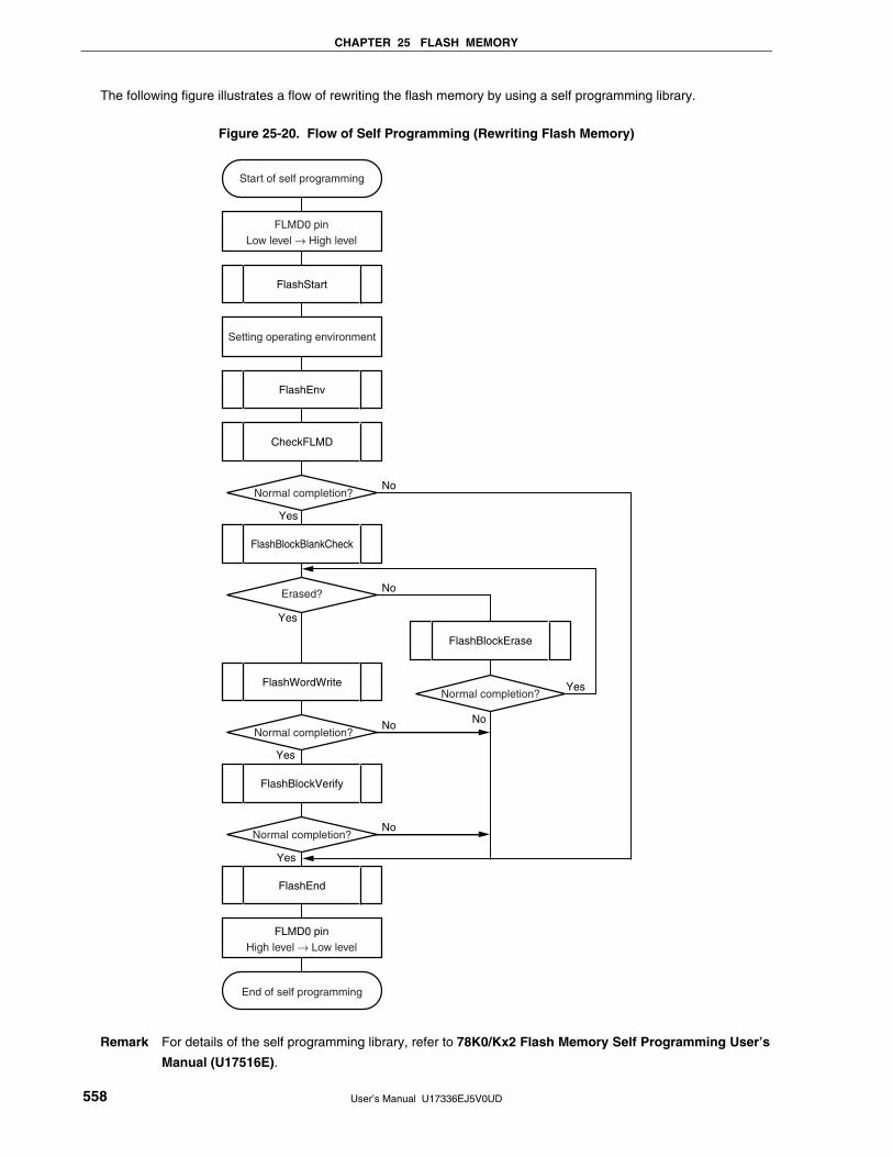
CHAPTER 25 FLASH MEMORY
User’s Manual U17336EJ5V0UD 558
The following figure illustrates a flow of rewriting the flash memory by using a self programming library.
Figure 25-20. Flow of Self Programming (Rewriting Flash Memory)
Start of self programming
FlashStart
FLMD0 pinLow level → High level
Normal completion?
Yes
No
Setting operating environment
FlashEnv
CheckFLMD
FlashBlockBlankCheck
Erased?
Yes
Yes
No
FlashBlockErase
Normal completion?FlashWordWrite
Normal completion?
FlashBlockVerify
Normal completion?
FlashEnd
FLMD0 pinHigh level → Low level
End of self programming
Yes
Yes
No
No
No
Remark For details of the self programming library, refer to 78K0/Kx2 Flash Memory Self Programming User’s
Manual (U17516E).

CHAPTER 25 FLASH MEMORY
User’s Manual U17336EJ5V0UD 559
The following table shows the processing time and interrupt response time for the self programming library.
Table 25-13. Processing Time for Self Programming Library (1/3)
(1) When internal high-speed oscillation clock is used and entry RAM is located outside short direct
addressing range
Processing Time (μs)
Normal Model of C Compiler Static Model of C Compiler/Assembler
Library Name
Min. Max. Min. Max.
Self programming start library 4.25
Initialize library 977.75
Mode check library 753.875 753.125
Block blank check library 12770.875 12765.875
Block erase library 36909.5 356318 36904.5 356296.25
Word write library 1214 (1214.375) 2409 (2409.375) 1207 (1207.375) 2402 (2402.375)
Block verify library 25618.875 25613.875
Self programming end library 4.25
Option value: 03H 871.25 (871.375) 866 (866.125)
Option value: 04H 863.375 (863.5) 858.125 (858.25)
Get information library
Option value: 05H 1024.75 (1043.625) 1037.5 (1038.375)
Set information library 105524.75 790809.375 105523.75 790808.375
EEPROM write library 1496.5
(1496.875)
2691.5
(2691.875)
1489.5
(1489.875)
2684.5
(2684.875)
(2) When internal high-speed oscillation clock is used and entry RAM is located in short direct addressing
range
Processing Time (μs)
Normal Model of C Compiler Static Model of C Compiler/Assembler
Library Name
Min. Max. Min. Max.
Self programming start library 4.25
Initialize library 443.5
Mode check library 219.625 218.875
Block blank check library 12236.625 12231.625
Block erase library 36363.25 355771.75 36358.25 355750
Word write library 679.75
(680.125)
1874.75
(1875.125)
672.75
(673.125)
1867.75
(1868.125)
Block verify library 25072.625 25067.625
Self programming end library 4.25
Option value: 03H 337 (337.125) 331.75 (331.875)
Option value: 04H 329.125 (239.25) 323.875 (324)
Get information library
Option value: 05H 502.25 (503.125) 497 (497.875)
Set information library 104978.5 541143.125 104977.5 541142.125
EEPROM write library 962.25
(962.625)
2157.25
(2157.625)
955.25
(955.625)
2150.25
(2150.625)
Remarks 1. Values in parentheses indicate values when a write start address structure is located other than in the
internal high-speed RAM.
2. The above processing times are those during stabilized operation of the internal high-speed oscillator
(RSTS = 1).
3. RSTS: Bit 7 of the internal oscillation mode register (RCM)
<R>

CHAPTER 25 FLASH MEMORY
User’s Manual U17336EJ5V0UD 560
Table 25-13. Processing Time for Self Programming Library (2/3)
(3) When high-speed system clock (X1 oscillation or external clock input) is used and entry RAM is located
outside short direct addressing range
Processing Time (μs)
Normal Model of C Compiler Static Model of C Compiler/Assembler
Library Name
Min. Max. Min. Max.
Self programming start library 34/fCPU
Initialize library 49/fCPU + 485.8125
Mode check library 35/fCPU + 374.75 29/fCPU + 374.75
Block blank check library 174/fCPU + 6382.0625 134/fCPU + 6382.0625
Block erase library 174/fCPU +
31093.875
174/fCPU +
298948.125
134/fCPU +
31093.875
134/fCPU +
298948.125
Word write library 318 (321)/fCPU +
644.125
318 (321)/fCPU +
1491.625
262 (265)/fCPU +
644.125
262 (265)/fCPU +
1491.625
Block verify library 174/fCPU + 13448.5625 134/fCPU + 13448.5625
Self programming end library 34/fCPU
Option value: 03H 171 (172 )/fCPU + 432.4375 129 (130)/fCPU + 432.4375
Option value: 04H 181 (182)/fCPU + 427.875 139 (140)/fCPU + 427.875
Get information library
Option value: 05H 404 (411)/fCPU + 496.125 362 (369)/fCPU + 496.125
Set information library 75/fCPU +
79157.6875
75/fCPU + 652400 67fCPU +
79157.6875
67fCPU + 652400
EEPROM write library 318 (321)/fCPU +
799.875
318 (321)/fCPU +
1647.375
262 (265)/fCPU +
799.875
262 (265)/fCPU +
1647.375
Remarks 1. Values in parentheses indicate values when a write start address structure is located other than in the
internal high-speed RAM.
2. The above processing times are those during stabilized operation of the internal high-speed oscillator
(RSTS = 1).
3. fCPU: CPU operation clock frequency
4. RSTS: Bit 7 of the internal oscillation mode register (RCM)
<R>

CHAPTER 25 FLASH MEMORY
User’s Manual U17336EJ5V0UD 561
Table 25-13. Processing Time for Self Programming Library (3/3)
(4) When high-speed system clock (X1 oscillation or external clock input) is used and entry RAM is located
in short direct addressing range
Processing Time (μs)
Normal Model of C Compiler Static Model of C Compiler/Assembler
Library Name
Min. Max. Min. Max.
Self programming start library 34/fCPU
Initialize library 49/fCPU + 224.6875
Mode check library 35/fCPU + 113.625 29/fCPU + 113.625
Block blank check library 174/fCPU + 6120.9375 134/fCPU + 6120.9375
Block erase library 174/fCPU +
30820.75
174/fCPU +
298675
134/fCPU +
30820.75
134/fCPU +
298675
Word write library 318 (321)/fCPU +
383
318 (321)/fCPU +
1230.5
262 (265)/fCPU +
383
262 (265)/fCPU +
1230.5
Block verify library 174/fCPU + 13175.4375 134/fCPU + 13175.4375
Self programming end library 34/fCPU
Option value: 03H 171 (172)/fCPU + 171.3125 129 (130)/fCPU + 171.3125
Option value: 04H 181 (182)/fCPU + 166.75 139 (140)/fCPU + 166.75
Get information library
Option value: 05H 404 (411)/fCPU + 231.875 362 (369)/fCPU + 231.875
Set information library 75/fCPU +
78884.5625
75/fCPU +
527566.875
67fCPU +
78884.5625
67fCPU +
527566.875
EEPROM write library 318 (321)/fCPU +
538.75
318 (321)/fCPU +
1386.25
262 (265)/fCPU +
538.75
262 (265)/fCPU +
1386.25
Remarks 1. Values in parentheses indicate values when a write start address structure is located other than in the
internal high-speed RAM.
2. The above processing times are those during stabilized operation of the internal high-speed oscillator
(RSTS = 1).
3. fCPU: CPU operation clock frequency
4. RSTS: Bit 7 of the internal oscillation mode register (RCM)
<R>

CHAPTER 25 FLASH MEMORY
User’s Manual U17336EJ5V0UD 562
Table 25-14. Interrupt Response Time for Self Programming Library (1/2)
(1) When internal high-speed oscillation clock is used
Interrupt Response Time (μs (Max.))
Normal Model of C Compiler Static Model of C Compiler/Assembler
Library Name
Entry RAM location
is outside short
direct addressing
range
Entry RAM location
is in short direct
addressing range
Entry RAM location
is outside short
direct addressing
range
Entry RAM location
is in short direct
addressing range
Block blank check library 933.6 668.6 927.9 662.9
Block erase library 1026.6 763.6 1020.9 757.9
Word write library 2505.8 1942.8 2497.8 1934.8
Block verify library 958.6 693.6 952.9 687.9
Set information library 476.5 211.5 475.5 210.5
EEPROM write library 2760.8 2168.8 2759.5 2167.5
Remarks 1. The above interrupt response times are those during stabilized operation of the internal high-speed
oscillator (RSTS = 1).
2. RSTS: Bit 7 of the internal oscillation mode register (RCM)
(2) When high-speed system clock is used (normal model of C compiler)
Interrupt Response Time (μs (Max.))
RSTOP = 0, RSTS = 1 RSTOP = 1
Library Name
Entry RAM location
is outside short
direct addressing
range
Entry RAM location
is in short direct
addressing range
Entry RAM location
is outside short
direct addressing
range
Entry RAM location
is in short direct
addressing range
Block blank check library 179/fCPU + 507 179/fCPU + 407 179/fCPU + 1650 179/fCPU + 714
Block erase library 179/fCPU + 559 179/fCPU + 460 179/fCPU + 1702 179/fCPU + 767
Word write library 333/fCPU + 1589 333/fCPU + 1298 333/fCPU + 2732 333/fCPU + 1605
Block verify library 179/fCPU + 518 179/fCPU + 418 179/fCPU + 1661 179/fCPU + 725
Set information library 80/fCPU + 370 80/fCPU + 165 80/fCPU + 1513 80/fCPU + 472
29/fCPU + 1759 29/fCPU + 1468 29/fCPU + 1759 29/fCPU + 1468 EEPROM write libraryNote
333/fCPU + 834 333/fCPU + 512 333/fCPU + 2061 333/fCPU + 873
Note The longer value of the EEPROM write library interrupt response time becomes the Max. value, depending
on the value of fCPU.
Remarks 1. fCPU: CPU operation clock frequency
2. RSTOP: Bit 0 of the internal oscillation mode register (RCM)
3. RSTS: Bit 7 of the internal oscillation mode register (RCM)
<R>

CHAPTER 25 FLASH MEMORY
User’s Manual U17336EJ5V0UD 563
Table 25-14. Interrupt Response Time for Self Programming Library (2/2)
(3) When high-speed system clock is used (static model of C compiler/assembler)
Interrupt Response Time (μs (Max.))
RSTOP = 0, RSTS = 1 RSTOP = 1
Library Name
Entry RAM location
is outside short
direct addressing
range
Entry RAM location
is in short direct
addressing range
Entry RAM location
is outside short
direct addressing
range
Entry RAM location
is in short direct
addressing range
Block blank check library 136/fCPU + 507 136/fCPU + 407 136/fCPU + 1650 136/fCPU + 714
Block erase library 136/fCPU + 559 136/fCPU + 460 136/fCPU + 1702 136/fCPU + 767
Word write library 272/fCPU + 1589 272/fCPU + 1298 272/fCPU + 2732 272/fCPU + 1605
Block verify library 136/fCPU + 518 136/fCPU + 418 136/fCPU + 1661 136/fCPU + 725
Set information library 72/fCPU + 370 72/fCPU + 165 72/fCPU + 1513 72/fCPU + 472
19/fCPU + 1759 19/fCPU + 1468 19/fCPU + 1759 19/fCPU + 1468 EEPROM write libraryNote
268/fCPU + 834 268/fCPU + 512 268/fCPU + 2061 268/fCPU + 873
Note The longer value of the EEPROM write library interrupt response time becomes the Max. value, depending
on the value of fCPU.
Remarks 1. fCPU: CPU operation clock frequency
2. RSTOP: Bit 0 of the internal oscillation mode register (RCM)
3. RSTS: Bit 7 of the internal oscillation mode register (RCM)
<R>
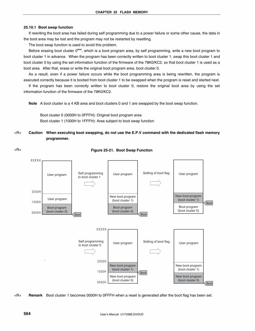
CHAPTER 25 FLASH MEMORY
User’s Manual U17336EJ5V0UD 564
25.10.1 Boot swap function
If rewriting the boot area has failed during self programming due to a power failure or some other cause, the data in
the boot area may be lost and the program may not be restarted by resetting.
The boot swap function is used to avoid this problem.
Before erasing boot cluster 0Note, which is a boot program area, by self programming, write a new boot program to
boot cluster 1 in advance. When the program has been correctly written to boot cluster 1, swap this boot cluster 1 and
boot cluster 0 by using the set information function of the firmware of the 78K0/KC2, so that boot cluster 1 is used as a
boot area. After that, erase or write the original boot program area, boot cluster 0.
As a result, even if a power failure occurs while the boot programming area is being rewritten, the program is
executed correctly because it is booted from boot cluster 1 to be swapped when the program is reset and started next.
If the program has been correctly written to boot cluster 0, restore the original boot area by using the set
information function of the firmware of the 78K0/KC2.
Note A boot cluster is a 4 KB area and boot clusters 0 and 1 are swapped by the boot swap function.
Boot cluster 0 (0000H to 0FFFH): Original boot program area
Boot cluster 1 (1000H to 1FFFH): Area subject to boot swap function
Caution When executing boot swapping, do not use the E.P.V command with the dedicated flash memory
programmer.
Figure 25-21. Boot Swap Function
Boot program(boot cluster 0)
New boot program(boot cluster 1)
User program Self programming to boot cluster 1
Self programming to boot cluster 0
Setting of boot flag
Setting of boot flag
User program
Boot program(boot cluster 0)
User program
New boot program(boot cluster 1)
New boot program(boot cluster 0)
User program
New boot program(boot cluster 1)
New boot program(boot cluster 0)
User program
New boot program(boot cluster 1)
Boot program(boot cluster 0)
User program
X X X X H
X X X X H
2 0 0 0 H
0 0 0 0 H
1 0 0 0 H
2 0 0 0 H
0 0 0 0 H
1 0 0 0 H
Boot Boot
Boot
Boot
Boot
Remark Boot cluster 1 becomes 0000H to 0FFFH when a reset is generated after the boot flag has been set.
<R>
<R>
<R>

CHAPTER 25 FLASH MEMORY
User’s Manual U17336EJ5V0UD 565
Figure 25-22. Example of Executing Boot Swapping
Boot cluster 1
Booted by boot cluster 0
Booted by boot cluster 1
Booted by boot cluster 0
Block number
Erasing block 4
Boot cluster 0
Program
Program
Boot program
1 0 0 0 H
0 0 0 0 H
1 0 0 0 H
0 0 0 0 H
0 0 0 0 H
1 0 0 0 H
Erasing block 5
Writing blocks 5 to 7 Boot swap
Boot swap
3210
7654
Boot program
Boot programBoot program
Program
Program
Program
Program
Boot program
3210
7654
Boot program
Boot programBoot program
Program
Program
Boot program
3210
7654
Boot program
Boot programBoot program
Program
Erasing block 6 Erasing block 7
Program
Boot program
3210
7654
Boot program
Boot programBoot program
Boot program
3210
7654
Boot program
Boot programBoot program
Boot program
3210
7654
Boot program
Boot programBoot program
New boot program
New boot program
New boot program
New boot program
Boot program
3210
7654
Boot program
Boot programBoot program
New boot program
New boot program
New boot program
New boot program
Erasing block 0 Erasing block 1
Erasing block 2 Erasing block 3
3210
7654
Boot program
Boot programBoot program
New boot program
New boot program
New boot program
New boot program
3210
7654
Boot programBoot program
New boot program
New boot program
New boot program
New boot program
3210
7654
Boot program
New boot program
New boot program
New boot program
New boot program
3210
7654 New boot program
New boot program
New boot program
New boot program
Writing blocks 0 to 3
3210
7654 New boot program
New boot program
New boot program
New boot program
New boot programNew boot programNew boot programNew boot program
3210
7654 New boot program
New boot program
New boot program
New boot program
New boot programNew boot programNew boot programNew boot program
<R>

User’s Manual U17336EJ5V0UD 566
CHAPTER 26 ON-CHIP DEBUG FUNCTION (μPD78F0513D AND 78F0515D ONLY)
26.1 Connecting QB-78K0MINI or QB-MINI2 to μPD78F0513D and 78F0515D
The μPD78F0513D and 78F0515D use the VDD, FLMD0, RESET, OCD0A/X1 (or OCD1A/P31), OCD0B/X2 (or
OCD1B/P32), and VSS pins to communicate with the host machine via an on-chip debug emulator (QB-78K0MINI or
QB-MINI2). Whether OCD0A/X1 and OCD1A/P31, or

CHAPTER 26 ON-CHIP DEBUG FUNCTION (μPD78F0513D AND 78F0515D ONLY)
User’s Manual U17336EJ5V0UD 567
Figure 26-2. Connection Example of QB-78K0MINI or QB-MINI2 and μPD78F0513D, 78F0515D
(When OCD1A/P31 and OCD1B/P32 Are Used)
VDD
Target device
FLMD0
OCD1A/P31
OCD1B/P32
Reset signal
RESET_INNote 1
X2 (DATA)Note 4
X1 (CLK)Note 4
FLMD0
RESET
VDD
RESET_OUT
GND
Target connector(10-pin)
GND
Note 3
VDD Reset circuitVDD VDD
GND
R.F.U.
R.F.U.
Note 3
1 kΩ(Recommended)
10 kΩ(Recommended)
(Open)
(Open)
VDD
3 to 10 kΩ(Recommended)Note 2
Notes 1. This connection is designed assuming that the reset signal is output from the N-ch open-drain buffer
(output resistance: 100 Ω or less). For details, refer to QB-78K0MINI User’s Manual (U17029E) or QB-
MINI2 User’s Manual (U18371E).
2. This is the processing of the pin when OCD1B/P32 is set as the input port (to prevent the pin from being
left opened when not connected to QB-78K0MINI or QB-MINI2).
3. Make pull-down resistor 470 Ω or more (10 kΩ: recommended).
4. Characters without parentheses represent the QB-78K0MINI name, and those within parenthesis the
QB-MINI2 name.
Connect the FLMD0 pin as follows when performing self programming by means of on-chip debugging.
Figure 26-3. Connection of FLMD0 Pin for Self Programming by Means of On-Chip Debugging
Target connector
FLMD0 FLMD0
Port
1 kΩ (recommended)
10 kΩ (recommended)
PD78F0513D, 78F0515Dμ

CHAPTER 26 ON-CHIP DEBUG FUNCTION (μPD78F0513D AND 78F0515D ONLY)
User’s Manual U17336EJ5V0UD 568
26.2 Reserved Area Used by QB-78K0MINI and QB-MINI2
QB-78K0MINI and QB-MINI2 use the reserved areas shown in Figure 26-4 below to implement communication with
the μPD78F0513D and 78F0515D, or each debug function. The shaded reserved areas are used for the respective
debug functions to be used, and the other areas are always used for debugging. These reserved areas can be
secured by using user programs and compiler options.
When using a boot swap operation during self programming, set the same value to boot cluster 1 beforehand.
For details on reserved area, refer to QB-78K0MINI User’s Manual (U17029E) or QB-MINI2 User’s Manual
(U18371E).
Figure 26-4. Reserved Area Used by QB-78K0MINI and QB-MINI2
Debug monitor area (2 bytes)
Software break area (2 bytes)
Security ID area(10 bytes)
Option byte area (1 byte)
Debug monitor area(257 bytes)
Pseudo RRM area(256 bytes)
Internal ROM space Internal RAM space
Stack area for debugging(Max. 16 bytes)
Pseudo RRM area(16 bytes)Note
FF7FH
F7F0H
2 8 F H
1 9 0 H1 8 F H
8 F H8EH
8 5 H8 4 H
7 F H7EH
0 3 H0 2 H
0 0 H
Note The securing of this area is not required for products (μPD78F0513D) that have no internal expansion RAM
incorporated.
Remark Shaded reserved areas: Area used for the respective debug functions to be used
Other reserved areas: Areas always used for debugging
<R>

User’s Manual U17336EJ5V0UD 569
CHAPTER 27 INSTRUCTION SET
This chapter lists each instruction set of the 78K0/KC2 in table form. For details of each operation and operation
code, refer to the separate document 78K/0 Series Instructions User’s Manual (U12326E).
27.1 Conventions Used in Operation List
27.1.1 Operand identifiers and specification methods
Operands are written in the “Operand” column of each instruction in accordance with the specification method of
the instruction operand identifier (refer to the assembler specifications for details). When there are two or more
methods, select one of them. Uppercase letters and the symbols #, !, $ and [ ] are keywords and must be written as
they are. Each symbol has the following meaning.
• #: Immediate data specification
• !: Absolute address specification
• $: Relative address specification
• [ ]: Indirect address specification
In the case of immediate data, describe an appropriate numeric value or a label. When using a label, be sure to
write the #, !, $, and [ ] symbols.
For operand register identifiers r and rp, either function names (X, A, C, etc.) or absolute names (names in
parentheses in the table below, R0, R1, R2, etc.) can be used for specification.
Table 27-1. Operand Identifiers and Specification Methods
Identifier Specification Method
r
rp
sfr
sfrp
X (R0), A (R1), C (R2), B (R3), E (R4), D (R5), L (R6), H (R7)
AX (RP0), BC (RP1), DE (RP2), HL (RP3)
Special function register symbolNote
Special function register symbol (16-bit manipulatable register even addresses only)Note
saddr
saddrp
FE20H to FF1FH Immediate data or labels
FE20H to FF1FH Immediate data or labels (even address only)
addr16
addr11
addr5
0000H to FFFFH Immediate data or labels
(Only even addresses for 16-bit data transfer instructions)
0800H to 0FFFH Immediate data or labels
0040H to 007FH Immediate data or labels (even address only)
word
byte
bit
16-bit immediate data or label
8-bit immediate data or label
3-bit immediate data or label
RBn RB0 to RB3
Note Addresses from FFD0H to FFDFH cannot be accessed with these operands.
Remark For special function register symbols, see Table 3-7 Special Function Register List.

CHAPTER 27 INSTRUCTION SET
User’s Manual U17336EJ5V0UD 570
27.1.2 Description of operation column
A: A register; 8-bit accumulator
X: X register
B: B register
C: C register
D: D register
E: E register
H: H register
L: L register
AX: AX register pair; 16-bit accumulator
BC: BC register pair
DE: DE register pair
HL: HL register pair
PC: Program counter
SP: Stack pointer
PSW: Program status word
CY: Carry flag
AC: Auxiliary carry flag
Z: Zero flag
RBS: Register bank select flag
IE: Interrupt request enable flag
( ): Memory contents indicated by address or register contents in parentheses
XH, XL: Higher 8 bits and lower 8 bits of 16-bit register
∧: Logical product (AND)
∨: Logical sum (OR)
∨: Exclusive logical sum (exclusive OR) ⎯⎯: Inverted data
addr16: 16-bit immediate data or label
jdisp8: Signed 8-bit data (displacement value)
27.1.3 Description of flag operation column
(Blank): Not affected
0: Cleared to 0
1: Set to 1
×: Set/cleared according to the result
R: Previously saved value is restored

CHAPTER 27 INSTRUCTION SET
User’s Manual U17336EJ5V0UD 571
27.2 Operation List
Clocks Flag Instruction
Group Mnemonic Operands Bytes
Note 1 Note 2 Operation
Z AC CY
r, #byte 2 4 − r ← byte
saddr, #byte 3 6 7 (saddr) ← byte
sfr, #byte 3 − 7 sfr ← byte
A, r Note 3 1 2 − A ← r
r, A Note 3 1 2 − r ← A
A, saddr 2 4 5 A ← (saddr)
saddr, A 2 4 5 (saddr) ← A
A, sfr 2 − 5 A ← sfr
sfr, A 2 − 5 sfr ← A
A, !addr16 3 8 9 A ← (addr16)
!addr16, A 3 8 9 (addr16) ← A
PSW, #byte 3 − 7 PSW ← byte × × ×
A, PSW 2 − 5 A ← PSW
PSW, A 2 − 5 PSW ← A × × ×
A, [DE] 1 4 5 A ← (DE)
[DE], A 1 4 5 (DE) ← A
A, [HL] 1 4 5 A ← (HL)
[HL], A 1 4 5 (HL) ← A
A, [HL + byte] 2 8 9 A ← (HL + byte)
[HL + byte], A 2 8 9 (HL + byte) ← A
A, [HL + B] 1 6 7 A ← (HL + B)
[HL + B], A 1 6 7 (HL + B) ← A
A, [HL + C] 1 6 7 A ← (HL + C)
MOV
[HL + C], A 1 6 7 (HL + C) ← A
A, r Note 3 1 2 − A ↔ r
A, saddr 2 4 6 A ↔ (saddr)
A, sfr 2 − 6 A ↔ (sfr)
A, !addr16 3 8 10 A ↔ (addr16)
A, [DE] 1 4 6 A ↔ (DE)
A, [HL] 1 4 6 A ↔ (HL)
A, [HL + byte] 2 8 10 A ↔ (HL + byte)
A, [HL + B] 2 8 10 A ↔ (HL + B)
8-bit data
transfer
XCH
A, [HL + C] 2 8 10 A ↔ (HL + C)
Notes 1. When the internal high-speed RAM area is accessed or for an instruction with no data access
2. When an area except the internal high-speed RAM area is accessed
3. Except “r = A”
Remarks 1. One instruction clock cycle is one cycle of the CPU clock (fCPU) selected by the processor clock
control register (PCC).
2. This clock cycle applies to the internal ROM program.

CHAPTER 27 INSTRUCTION SET
User’s Manual U17336EJ5V0UD 572
Clocks Flag Instruction
Group Mnemonic Operands Bytes
Note 1 Note 2 Operation
Z AC CY
rp, #word 3 6 − rp ← word
saddrp, #word 4 8 10 (saddrp) ← word
sfrp, #word 4 − 10 sfrp ← word
AX, saddrp 2 6 8 AX ← (saddrp)
saddrp, AX 2 6 8 (saddrp) ← AX
AX, sfrp 2 − 8 AX ← sfrp
sfrp, AX 2 − 8 sfrp ← AX
AX, rp Note 3 1 4 − AX ← rp
rp, AX Note 3 1 4 − rp ← AX
AX, !addr16 3 10 12 AX ← (addr16)
MOVW
!addr16, AX 3 10 12 (addr16) ← AX
16-bit data
transfer
XCHW AX, rp Note 3 1 4 − AX ↔ rp
A, #byte 2 4 − A, CY ← A + byte × × ×
saddr, #byte 3 6 8 (saddr), CY ← (saddr) + byte × × ×
A, r Note 4 2 4 − A, CY ← A + r × × ×
r, A 2 4 − r, CY ← r + A × × ×
A, saddr 2 4 5 A, CY ← A + (saddr) × × ×
A, !addr16 3 8 9 A, CY ← A + (addr16) × × ×
A, [HL] 1 4 5 A, CY ← A + (HL) × × ×
A, [HL + byte] 2 8 9 A, CY ← A + (HL + byte) × × ×
A, [HL + B] 2 8 9 A, CY ← A + (HL + B) × × ×
ADD
A, [HL + C] 2 8 9 A, CY ← A + (HL + C) × × ×
A, #byte 2 4 − A, CY ← A + byte + CY × × ×
saddr, #byte 3 6 8 (saddr), CY ← (saddr) + byte + CY × × ×
A, r Note 4 2 4 − A, CY ← A + r + CY × × ×
r, A 2 4 − r, CY ← r + A + CY × × ×
A, saddr 2 4 5 A, CY ← A + (saddr) + CY × × ×
A, !addr16 3 8 9 A, CY ← A + (addr16) + C × × ×
A, [HL] 1 4 5 A, CY ← A + (HL) + CY × × ×
A, [HL + byte] 2 8 9 A, CY ← A + (HL + byte) + CY × × ×
A, [HL + B] 2 8 9 A, CY ← A + (HL + B) + CY × × ×
8-bit
operation
ADDC
A, [HL + C] 2 8 9 A, CY ← A + (HL + C) + CY × × ×
Notes 1. When the internal high-speed RAM area is accessed or for an instruction with no data access
2. When an area except the internal high-speed RAM area is accessed
3. Only when rp = BC, DE or HL
4. Except “r = A”
Remarks 1. One instruction clock cycle is one cycle of the CPU clock (fCPU) selected by the processor clock
control register (PCC).
2. This clock cycle applies to the internal ROM program.
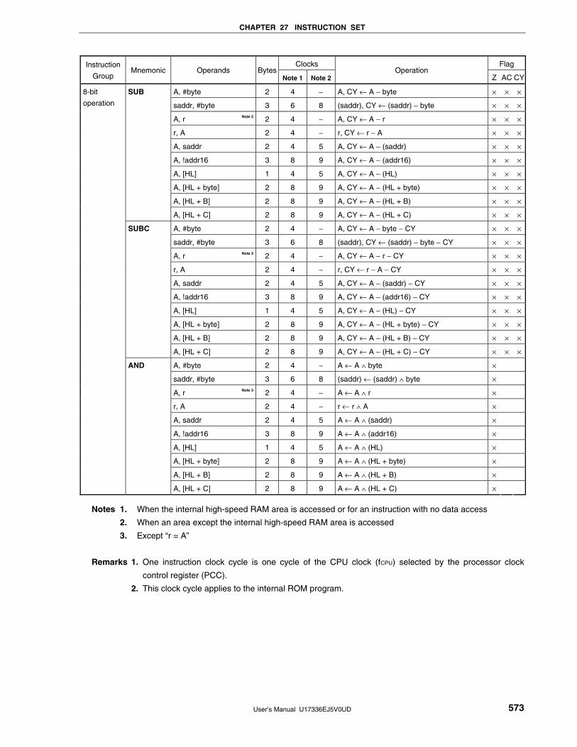
CHAPTER 27 INSTRUCTION SET
User’s Manual U17336EJ5V0UD 573
Clocks Flag Instruction
Group Mnemonic Operands Bytes
Note 1 Note 2 Operation
Z AC CY
A, #byte 2 4 − A, CY ← A − byte × × ×
saddr, #byte 3 6 8 (saddr), CY ← (saddr) − byte × × ×
A, r Note 3 2 4 − A, CY ← A − r × × ×
r, A 2 4 − r, CY ← r − A × × ×
A, saddr 2 4 5 A, CY ← A − (saddr) × × ×
A, !addr16 3 8 9 A, CY ← A − (addr16) × × ×
A, [HL] 1 4 5 A, CY ← A − (HL) × × ×
A, [HL + byte] 2 8 9 A, CY ← A − (HL + byte) × × ×
A, [HL + B] 2 8 9 A, CY ← A − (HL + B) × × ×
SUB
A, [HL + C] 2 8 9 A, CY ← A − (HL + C) × × ×
A, #byte 2 4 − A, CY ← A − byte − CY × × ×
saddr, #byte 3 6 8 (saddr), CY ← (saddr) − byte − CY × × ×
A, r Note 3 2 4 − A, CY ← A − r − CY × × ×
r, A 2 4 − r, CY ← r − A − CY × × ×
A, saddr 2 4 5 A, CY ← A − (saddr) − CY × × ×
A, !addr16 3 8 9 A, CY ← A − (addr16) − CY × × ×
A, [HL] 1 4 5 A, CY ← A − (HL) − CY × × ×
A, [HL + byte] 2 8 9 A, CY ← A − (HL + byte) − CY × × ×
A, [HL + B] 2 8 9 A, CY ← A − (HL + B) − CY × × ×
SUBC
A, [HL + C] 2 8 9 A, CY ← A − (HL + C) − CY × × ×
A, #byte 2 4 − A ← A ∧ byte ×
saddr, #byte 3 6 8 (saddr) ← (saddr) ∧ byte ×
A, r Note 3 2 4 − A ← A ∧ r ×
r, A 2 4 − r ← r ∧ A ×
A, saddr 2 4 5 A ← A ∧ (saddr) ×
A, !addr16 3 8 9 A ← A ∧ (addr16) ×
A, [HL] 1 4 5 A ← A ∧ (HL) ×
A, [HL + byte] 2 8 9 A ← A ∧ (HL + byte) ×
A, [HL + B] 2 8 9 A ← A ∧ (HL + B) ×
8-bit
operation
AND
A, [HL + C] 2 8 9 A ← A ∧ (HL + C) ×
Notes 1. When the internal high-speed RAM area is accessed or for an instruction with no data access
2. When an area except the internal high-speed RAM area is accessed
3. Except “r = A”
Remarks 1. One instruction clock cycle is one cycle of the CPU clock (fCPU) selected by the processor clock
control register (PCC).
2. This clock cycle applies to the internal ROM program.
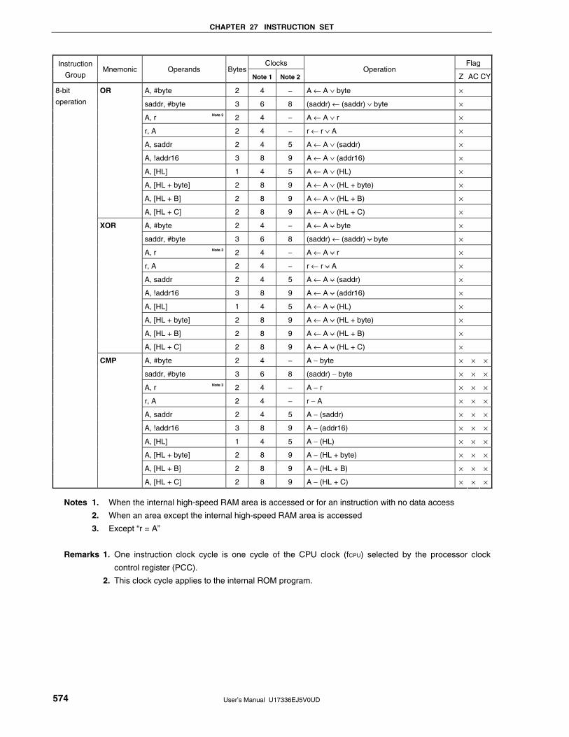
CHAPTER 27 INSTRUCTION SET
User’s Manual U17336EJ5V0UD 574
Clocks Flag Instruction
Group Mnemonic Operands Bytes
Note 1 Note 2 Operation
Z AC CY
A, #byte 2 4 − A ← A ∨ byte ×
saddr, #byte 3 6 8 (saddr) ← (saddr) ∨ byte ×
A, r Note 3 2 4 − A ← A ∨ r ×
r, A 2 4 − r ← r ∨ A ×
A, saddr 2 4 5 A ← A ∨ (saddr) ×
A, !addr16 3 8 9 A ← A ∨ (addr16) ×
A, [HL] 1 4 5 A ← A ∨ (HL) ×
A, [HL + byte] 2 8 9 A ← A ∨ (HL + byte) ×
A, [HL + B] 2 8 9 A ← A ∨ (HL + B) ×
OR
A, [HL + C] 2 8 9 A ← A ∨ (HL + C) ×
A, #byte 2 4 − A ← A ∨ byte ×
saddr, #byte 3 6 8 (saddr) ← (saddr) ∨ byte ×
A, r Note 3 2 4 − A ← A ∨ r ×
r, A 2 4 − r ← r ∨ A ×
A, saddr 2 4 5 A ← A ∨ (saddr) ×
A, !addr16 3 8 9 A ← A ∨ (addr16) ×
A, [HL] 1 4 5 A ← A ∨ (HL) ×
A, [HL + byte] 2 8 9 A ← A ∨ (HL + byte) ×
A, [HL + B] 2 8 9 A ← A ∨ (HL + B) ×
XOR
A, [HL + C] 2 8 9 A ← A ∨ (HL + C) ×
A, #byte 2 4 − A − byte × × ×
saddr, #byte 3 6 8 (saddr) − byte × × ×
A, r Note 3 2 4 − A − r × × ×
r, A 2 4 − r − A × × ×
A, saddr 2 4 5 A − (saddr) × × ×
A, !addr16 3 8 9 A − (addr16) × × ×
A, [HL] 1 4 5 A − (HL) × × ×
A, [HL + byte] 2 8 9 A − (HL + byte) × × ×
A, [HL + B] 2 8 9 A − (HL + B) × × ×
8-bit
operation
CMP
A, [HL + C] 2 8 9 A − (HL + C) × × ×
Notes 1. When the internal high-speed RAM area is accessed or for an instruction with no data access
2. When an area except the internal high-speed RAM area is accessed
3. Except “r = A”
Remarks 1. One instruction clock cycle is one cycle of the CPU clock (fCPU) selected by the processor clock
control register (PCC).
2. This clock cycle applies to the internal ROM program.
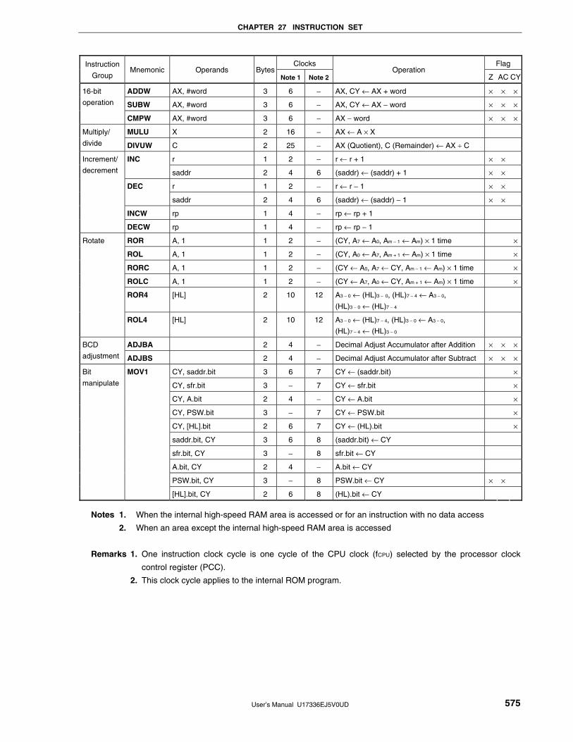
CHAPTER 27 INSTRUCTION SET
User’s Manual U17336EJ5V0UD 575
Clocks Flag Instruction
Group Mnemonic Operands Bytes
Note 1 Note 2 Operation
Z AC CY
ADDW AX, #word 3 6 − AX, CY ← AX + word × × ×
SUBW AX, #word 3 6 − AX, CY ← AX − word × × ×
16-bit
operation
CMPW AX, #word 3 6 − AX − word × × ×
MULU X 2 16 − AX ← A × X Multiply/
divide DIVUW C 2 25 − AX (Quotient), C (Remainder) ← AX ÷ C
r 1 2 − r ← r + 1 × × INC
saddr 2 4 6 (saddr) ← (saddr) + 1 × ×
r 1 2 − r ← r − 1 × × DEC
saddr 2 4 6 (saddr) ← (saddr) − 1 × ×
INCW rp 1 4 − rp ← rp + 1
Increment/
decrement
DECW rp 1 4 − rp ← rp − 1
ROR A, 1 1 2 − (CY, A7 ← A0, Am − 1 ← Am) × 1 time ×
ROL A, 1 1 2 − (CY, A0 ← A7, Am + 1 ← Am) × 1 time ×
RORC A, 1 1 2 − (CY ← A0, A7 ← CY, Am − 1 ← Am) × 1 time ×
ROLC A, 1 1 2 − (CY ← A7, A0 ← CY, Am + 1 ← Am) × 1 time ×
ROR4 [HL] 2 10 12 A3 − 0 ← (HL)3 − 0, (HL)7 − 4 ← A3 − 0,
(HL)3 − 0 ← (HL)7 − 4
Rotate
ROL4 [HL] 2 10 12 A3 − 0 ← (HL)7 − 4, (HL)3 − 0 ← A3 − 0,
(HL)7 − 4 ← (HL)3 − 0
ADJBA 2 4 − Decimal Adjust Accumulator after Addition × × ×BCD
adjustment ADJBS 2 4 − Decimal Adjust Accumulator after Subtract × × ×
CY, saddr.bit 3 6 7 CY ← (saddr.bit) ×
CY, sfr.bit 3 − 7 CY ← sfr.bit ×
CY, A.bit 2 4 − CY ← A.bit ×
CY, PSW.bit 3 − 7 CY ← PSW.bit ×
CY, [HL].bit 2 6 7 CY ← (HL).bit ×
saddr.bit, CY 3 6 8 (saddr.bit) ← CY
sfr.bit, CY 3 − 8 sfr.bit ← CY
A.bit, CY 2 4 − A.bit ← CY
PSW.bit, CY 3 − 8 PSW.bit ← CY × ×
Bit
manipulate
MOV1
[HL].bit, CY 2 6 8 (HL).bit ← CY
Notes 1. When the internal high-speed RAM area is accessed or for an instruction with no data access
2. When an area except the internal high-speed RAM area is accessed
Remarks 1. One instruction clock cycle is one cycle of the CPU clock (fCPU) selected by the processor clock
control register (PCC).
2. This clock cycle applies to the internal ROM program.

CHAPTER 27 INSTRUCTION SET
User’s Manual U17336EJ5V0UD 576
Clocks Flag Instruction
Group Mnemonic Operands Bytes
Note 1 Note 2 Operation
Z AC CY
CY, saddr.bit 3 6 7 CY ← CY ∧ (saddr.bit) ×
CY, sfr.bit 3 − 7 CY ← CY ∧ sfr.bit ×
CY, A.bit 2 4 − CY ← CY ∧ A.bit ×
CY, PSW.bit 3 − 7 CY ← CY ∧ PSW.bit ×
AND1
CY, [HL].bit 2 6 7 CY ← CY ∧ (HL).bit ×
CY, saddr.bit 3 6 7 CY ← CY ∨ (saddr.bit) ×
CY, sfr.bit 3 − 7 CY ← CY ∨ sfr.bit ×
CY, A.bit 2 4 − CY ← CY ∨ A.bit ×
CY, PSW.bit 3 − 7 CY ← CY ∨ PSW.bit ×
OR1
CY, [HL].bit 2 6 7 CY ← CY ∨ (HL).bit ×
CY, saddr.bit 3 6 7 CY ← CY ∨ (saddr.bit) ×
CY, sfr.bit 3 − 7 CY ← CY ∨ sfr.bit ×
CY, A.bit 2 4 − CY ← CY ∨ A.bit ×
CY, PSW. bit 3 − 7 CY ← CY ∨ PSW.bit ×
XOR1
CY, [HL].bit 2 6 7 CY ← CY ∨ (HL).bit ×
saddr.bit 2 4 6 (saddr.bit) ← 1
sfr.bit 3 − 8 sfr.bit ← 1
A.bit 2 4 − A.bit ← 1
PSW.bit 2 − 6 PSW.bit ← 1 × × ×
SET1
[HL].bit 2 6 8 (HL).bit ← 1
saddr.bit 2 4 6 (saddr.bit) ← 0
sfr.bit 3 − 8 sfr.bit ← 0
A.bit 2 4 − A.bit ← 0
PSW.bit 2 − 6 PSW.bit ← 0 × × ×
CLR1
[HL].bit 2 6 8 (HL).bit ← 0
SET1 CY 1 2 − CY ← 1 1
CLR1 CY 1 2 − CY ← 0 0
Bit
manipulate
NOT1 CY 1 2 − CY ← CY ×
Notes 1. When the internal high-speed RAM area is accessed or for an instruction with no data access
2. When an area except the internal high-speed RAM area is accessed
Remarks 1. One instruction clock cycle is one cycle of the CPU clock (fCPU) selected by the processor clock
control register (PCC).
2. This clock cycle applies to the internal ROM program.

CHAPTER 27 INSTRUCTION SET
User’s Manual U17336EJ5V0UD 577
Clocks Flag Instruction
Group Mnemonic Operands Bytes
Note 1 Note 2 Operation
Z AC CY
CALL !addr16 3 7 − (SP − 1) ← (PC + 3)H, (SP − 2) ← (PC + 3)L,
PC ← addr16, SP ← SP − 2
CALLF !addr11 2 5 − (SP − 1) ← (PC + 2)H, (SP − 2) ← (PC + 2)L,
PC15 − 11 ← 00001, PC10 − 0 ← addr11,
SP ← SP − 2
CALLT [addr5] 1 6 − (SP − 1) ← (PC + 1)H, (SP − 2) ← (PC + 1)L,
PCH ← (00000000, addr5 + 1),
PCL ← (00000000, addr5),
SP ← SP − 2
BRK 1 6 − (SP − 1) ← PSW, (SP − 2) ← (PC + 1)H,
(SP − 3) ← (PC + 1)L, PCH ← (003FH),
PCL ← (003EH), SP ← SP − 3, IE ← 0
RET 1 6 − PCH ← (SP + 1), PCL ← (SP),
SP ← SP + 2
RETI 1 6 − PCH ← (SP + 1), PCL ← (SP),
PSW ← (SP + 2), SP ← SP + 3
R R R
Call/return
RETB 1 6 − PCH ← (SP + 1), PCL ← (SP),
PSW ← (SP + 2), SP ← SP + 3
R R R
PSW 1 2 − (SP − 1) ← PSW, SP ← SP − 1 PUSH
rp 1 4 − (SP − 1) ← rpH, (SP − 2) ← rpL,
SP ← SP − 2
PSW 1 2 − PSW ← (SP), SP ← SP + 1 R R RPOP
rp 1 4 − rpH ← (SP + 1), rpL ← (SP),
SP ← SP + 2
SP, #word 4 − 10 SP ← word
SP, AX 2 − 8 SP ← AX
Stack
manipulate
MOVW
AX, SP 2 − 8 AX ← SP
!addr16 3 6 − PC ← addr16
$addr16 2 6 − PC ← PC + 2 + jdisp8
Unconditional
branch
BR
AX 2 8 − PCH ← A, PCL ← X
BC $addr16 2 6 − PC ← PC + 2 + jdisp8 if CY = 1
BNC $addr16 2 6 − PC ← PC + 2 + jdisp8 if CY = 0
BZ $addr16 2 6 − PC ← PC + 2 + jdisp8 if Z = 1
Conditional
branch
BNZ $addr16 2 6 − PC ← PC + 2 + jdisp8 if Z = 0
Notes 1. When the internal high-speed RAM area is accessed or for an instruction with no data access
2. When an area except the internal high-speed RAM area is accessed
Remarks 1. One instruction clock cycle is one cycle of the CPU clock (fCPU) selected by the processor clock
control register (PCC).
2. This clock cycle applies to the internal ROM program.

CHAPTER 27 INSTRUCTION SET
User’s Manual U17336EJ5V0UD 578
Clocks Flag Instruction
Group Mnemonic Operands Bytes
Note 1 Note 2 Operation
Z AC CY
saddr.bit, $addr16 3 8 9 PC ← PC + 3 + jdisp8 if (saddr.bit) = 1
sfr.bit, $addr16 4 − 11 PC ← PC + 4 + jdisp8 if sfr.bit = 1
A.bit, $addr16 3 8 − PC ← PC + 3 + jdisp8 if A.bit = 1
PSW.bit, $addr16 3 − 9 PC ← PC + 3 + jdisp8 if PSW.bit = 1
BT
[HL].bit, $addr16 3 10 11 PC ← PC + 3 + jdisp8 if (HL).bit = 1
saddr.bit, $addr16 4 10 11 PC ← PC + 4 + jdisp8 if (saddr.bit) = 0
sfr.bit, $addr16 4 − 11 PC ← PC + 4 + jdisp8 if sfr.bit = 0
A.bit, $addr16 3 8 − PC ← PC + 3 + jdisp8 if A.bit = 0
PSW.bit, $addr16 4 − 11 PC ← PC + 4 + jdisp8 if PSW. bit = 0
BF
[HL].bit, $addr16 3 10 11 PC ← PC + 3 + jdisp8 if (HL).bit = 0
saddr.bit, $addr16 4 10 12 PC ← PC + 4 + jdisp8 if (saddr.bit) = 1
then reset (saddr.bit)
sfr.bit, $addr16 4 − 12 PC ← PC + 4 + jdisp8 if sfr.bit = 1
then reset sfr.bit
A.bit, $addr16 3 8 − PC ← PC + 3 + jdisp8 if A.bit = 1
then reset A.bit
PSW.bit, $addr16 4 − 12 PC ← PC + 4 + jdisp8 if PSW.bit = 1
then reset PSW.bit
× × ×
BTCLR
[HL].bit, $addr16 3 10 12 PC ← PC + 3 + jdisp8 if (HL).bit = 1
then reset (HL).bit
B, $addr16 2 6 − B ← B − 1, then
PC ← PC + 2 + jdisp8 if B ≠ 0
C, $addr16 2 6 − C ← C −1, then
PC ← PC + 2 + jdisp8 if C ≠ 0
Conditional
branch
DBNZ
saddr, $addr16 3 8 10 (saddr) ← (saddr) − 1, then
PC ← PC + 3 + jdisp8 if (saddr) ≠ 0
SEL RBn 2 4 − RBS1, 0 ← n
NOP 1 2 − No Operation
EI 2 − 6 IE ← 1 (Enable Interrupt)
DI 2 − 6 IE ← 0 (Disable Interrupt)
HALT 2 6 − Set HALT Mode
CPU
control
STOP 2 6 − Set STOP Mode
Notes 1. When the internal high-speed RAM area is accessed or for an instruction with no data access
2. When an area except the internal high-speed RAM area is accessed
Remarks 1. One instruction clock cycle is one cycle of the CPU clock (fCPU) selected by the processor clock
control register (PCC).
2. This clock cycle applies to the internal ROM program.

CHAPTER 27 INSTRUCTION SET
User’s Manual U17336EJ5V0UD 579
27.3 Instructions Listed by Addressing Type
(1) 8-bit instructions
MOV, XCH, ADD, ADDC, SUB, SUBC, AND, OR, XOR, CMP, MULU, DIVUW, INC, DEC, ROR, ROL, RORC,
ROLC, ROR4, ROL4, PUSH, POP, DBNZ
Second Operand
First Operand
#byte A rNote sfr saddr !addr16 PSW [DE] [HL] [HL + byte]
[HL + B]
[HL + C]
$addr16 1 None
A ADD
ADDC
SUB
SUBC
AND
OR
XOR
CMP
MOV
XCH
ADD
ADDC
SUB
SUBC
AND
OR
XOR
CMP
MOV
XCH
MOV
XCH
ADD
ADDC
SUB
SUBC
AND
OR
XOR
CMP
MOV
XCH
ADD
ADDC
SUB
SUBC
AND
OR
XOR
CMP
MOV MOV
XCH
MOV
XCH
ADD
ADDC
SUB
SUBC
AND
OR
XOR
CMP
MOV
XCH
ADD
ADDC
SUB
SUBC
AND
OR
XOR
CMP
ROR
ROL
RORC
ROLC
r MOV MOV
ADD
ADDC
SUB
SUBC
AND
OR
XOR
CMP
INC
DEC
B, C DBNZ
sfr MOV MOV
saddr MOV
ADD
ADDC
SUB
SUBC
AND
OR
XOR
CMP
MOV DBNZ INC
DEC
!addr16 MOV
PSW MOV MOV PUSH
POP
[DE] MOV
[HL] MOV ROR4
ROL4
[HL + byte]
[HL + B]
[HL + C]
MOV
X MULU
C DIVUW
Note Except “r = A”

CHAPTER 27 INSTRUCTION SET
User’s Manual U17336EJ5V0UD 580
(2) 16-bit instructions
MOVW, XCHW, ADDW, SUBW, CMPW, PUSH, POP, INCW, DECW
Second Operand
First Operand
#word AX rpNote sfrp saddrp !addr16 SP None
AX ADDW
SUBW
CMPW
MOVW
XCHW
MOVW MOVW MOVW MOVW
rp MOVW MOVWNote INCW
DECW
PUSH
POP
sfrp MOVW MOVW
saddrp MOVW MOVW
!addr16 MOVW
SP MOVW MOVW
Note Only when rp = BC, DE, HL
(3) Bit manipulation instructions
MOV1, AND1, OR1, XOR1, SET1, CLR1, NOT1, BT, BF, BTCLR
Second Operand
First Operand
A.bit sfr.bit saddr.bit PSW.bit [HL].bit CY $addr16 None
A.bit MOV1 BT
BF
BTCLR
SET1
CLR1
sfr.bit MOV1 BT
BF
BTCLR
SET1
CLR1
saddr.bit MOV1 BT
BF
BTCLR
SET1
CLR1
PSW.bit MOV1 BT
BF
BTCLR
SET1
CLR1
[HL].bit MOV1 BT
BF
BTCLR
SET1
CLR1
CY MOV1
AND1
OR1
XOR1
MOV1
AND1
OR1
XOR1
MOV1
AND1
OR1
XOR1
MOV1
AND1
OR1
XOR1
MOV1
AND1
OR1
XOR1
SET1
CLR1
NOT1

CHAPTER 27 INSTRUCTION SET
User’s Manual U17336EJ5V0UD 581
(4) Call instructions/branch instructions
CALL, CALLF, CALLT, BR, BC, BNC, BZ, BNZ, BT, BF, BTCLR, DBNZ
Second Operand
First Operand
AX !addr16 !addr11 [addr5] $addr16
Basic instruction BR CALL
BR
CALLF CALLT BR
BC
BNC
BZ
BNZ
Compound
instruction
BT
BF
BTCLR
DBNZ
(5) Other instructions
ADJBA, ADJBS, BRK, RET, RETI, RETB, SEL, NOP, EI, DI, HALT, STOP

User’s Manual U17336EJ5V0UD 582
CHAPTER 28 ELECTRICAL SPECIFICATIONS (STANDARD PRODUCTS)
Target products: μPD78F0511, 78F0512, 78F0513, 78F0514, 78F0515, 78F0513D, 78F0515D
Caution The μPD78F0513D and 78F0515D have an on-chip debug function. Do not use these products for
mass production because its reliability cannot be guaranteed after the on-chip debug function
has been used, given the issue of the number of times the flash memory can be rewritten. NEC
Electronics does not accept complaints concerning these products.
Absolute Maximum Ratings (TA = 25°C) (1/2)
Parameter Symbol Conditions Ratings Unit
VDD −0.5 to +6.5 V
VSS −0.5 to +0.3 V
AVREF −0.5 to VDD + 0.3Note 1 V
Supply voltage
AVSS −0.5 to +0.3 V
REGC pin input voltage VIREGC –0.5 to +3.6 and ≤ VDD V
VI1 P00, P01, P10 to P17, P20 to P25,
P26Note 2, P27Note 2, P30 to P33, P40Note 2,
P41Note 2, P70, P71, P72Note 2, P73Note 2,
P74Note 3, P75Note 3, P120 to P124, P140Note 3,
X1, X2, XT1, XT2, RESET, FLMD0
−0.3 to VDD + 0.3Note 1 V Input voltage
VI2 P60 to P63 (N-ch open drain) −0.3 to +6.5 V
Output voltage VO −0.3 to VDD + 0.3Note 1 V
Analog input voltage VAN ANI0 to ANI5, ANI6Note 2, ANI7Note 2 −0.3 to AVREF + 0.3Note 1
and −0.3 to VDD + 0.3Note 1
V
Notes 1. Must be 6.5 V or lower.
2. 44-pin and 48-pin products only.
3. 48-pin products only.
Caution Product quality may suffer if the absolute maximum rating is exceeded even momentarily for any
parameter. That is, the absolute maximum ratings are rated values at which the product is on the
verge of suffering physical damage, and therefore the product must be used under conditions that
ensure that the absolute maximum ratings are not exceeded.
Remark Unless specified otherwise, the characteristics of alternate-function pins are the same as those of port pins.
<R>
<R>
<R>

CHAPTER 28 ELECTRICAL SPECIFICATIONS (STANDARD PRODUCTS)
User’s Manual U17336EJ5V0UD 583
Standard products
Absolute Maximum Ratings (TA = 25°C) (2/2)
Parameter Symbol Conditions Ratings Unit
Per pin P00, P01, P10 to P17,
P30 to P33, P40Note 1,
P41Note 1, P70, P71,
P72Note 1, P73Note 1,
P74Note 2, P75Note 2, P120,
P130Note 2, P140Note 2
−10 mA
P00, P01, P40Note 1,
P41Note 1, P120, P130Note 2,
P140Note 2
−25 mA Total of all pins
−80 mA
P10 to P17, P30 to P33,
P70, P71, P72Note 1,
P73Note 1, P74Note 2, P75Note 2
−55 mA
Per pin −0.5 mA
Total of all pins
P20 to P25, P26Note 1,
P27 Note 1 −2 mA
Per pin −1 mA
Output current, high IOH
Total of all pins
P121 to P124
−4 mA
Per pin P00, P01, P10 to P17,
P30 to P33, P40Note 1,
P41Note 1, P60 to P63,
P70, P71, P72 Note 1,
P73Note 1, P74Note 2,
P75Note 2, P120, P130Note 2,
P140Note 2
30 mA
P00, P01, P40Note 1,
P41Note 1, P120, P130Note 2,
P140Note 2
60 mA Total of all pins
200 mA
P10 to P17, P30 to P33,
P60 to P63, P70, P71,
P72Note 1, P73Note 1,
P74Note 2, P75Note 2
140 mA
Per pin 1 mA
Total of all pins
P20 to P25, P26Note 1,
P27Note 1 5 mA
Per pin 4 mA
Output current, low IOL
Total of all pins
P121 to P124
10 mA
Operating ambient
temperature
TA −40 to +85 °C
Storage temperature Tstg −65 to +150 °C
Notes 1. 44-pin and 48-pin products only.
2. 48-pin products only.
Caution Product quality may suffer if the absolute maximum rating is exceeded even momentarily for any
parameter. That is, the absolute maximum ratings are rated values at which the product is on the
verge of suffering physical damage, and therefore the product must be used under conditions that
ensure that the absolute maximum ratings are not exceeded.
Remark Unless specified otherwise, the characteristics of alternate-function pins are the same as those of port pins.
<R>
<R>
CHAPTER 28 ELECTRICAL SPECIFICATIONS (STANDARD PRODUCTS)
User’s Manual U17336EJ5V0UD 584
Standard products
X1 Oscillator Characteristics
(TA = −

CHAPTER 28 ELECTRICAL SPECIFICATIONS (STANDARD PRODUCTS)
User’s Manual U17336EJ5V0UD 585
Standard products
Internal Oscillator Characteristics
(TA = −40 to +85°C, 1.8 V ≤ VDD ≤ 5.5 V, VSS = AVSS = 0 V)
Resonator Parameter Conditions MIN. TYP. MAX. Unit
2.7 V ≤ VDD ≤ 5.5 V 7.6 8.0 8.4 MHz RSTS = 1
1.8 V ≤ VDD < 2.7 V 7.6 8.0 10.4 MHz
8 MHz internal oscillator Internal high-speed oscillation
clock frequency (fRH)Note
RSTS = 0 2.48 5.6 9.86 MHz
2.7 V ≤ VDD ≤ 5.5 V 216 240 264 kHz 240 kHz internal oscillator Internal low-speed oscillation
clock frequency (fRL) 1.8 V ≤ VDD < 2.7 V 192 240 264 kHz
Note Indicates only oscillator characteristics. Refer to AC Characteristics for instruction execution time.
Remark RSTS: Bit 7 of the internal oscillation mode register (RCM)
XT1 Oscillator Characteristics
(TA = −40 to +85°C, 1.8 V ≤ VDD ≤ 5.5 V, VSS = AVSS = 0 V)
Resonator Recommended Circuit Parameter Conditions MIN. TYP. MAX. Unit
Crystal
resonator
XT1VSS XT2
C4 C3
Rd
XT1 clock oscillation
frequency (fXT)Note
32 32.768 35 kHz
Note Indicates only oscillator characteristics. Refer to AC Characteristics for instruction execution time.
Cautions 1. When using the XT1 oscillator, wire as follows in the area enclosed by the broken lines in the
above figure to avoid an adverse effect from wiring capacitance.
• Keep the wiring length as short as possible.
• Do not cross the wiring with the other signal lines.
• Do not route the wiring near a signal line through which a high fluctuating current flows.
• Always make the ground point of the oscillator capacitor the same potential as VSS.
• Do not ground the capacitor to a ground pattern through which a high current flows.
• Do not fetch signals from the oscillator.
2. The XT1 oscillator is designed as a low-amplitude circuit for reducing power consumption, and
is more prone to malfunction due to noise than the X1 oscillator. Particular care is therefore
required with the wiring method when the XT1 clock is used.
<R>

CHAPTER 28 ELECTRICAL SPECIFICATIONS (STANDARD PRODUCTS)
User’s Manual U17336EJ5V0UD 586
Standard products
Recommended Oscillator Constants
(1) X1 oscillation: Ceramic resonator (TA = −40 to +85°C) (1/2)
Recommended Circuit
Constants
Oscillation Voltage Range Manufacturer Part Number SMD/
Lead
Frequency
(MHz)
C1 (pF) C2 (pF) MIN. (V) MAX. (V)
CSTCC2M00G56-R0 SMD 2.00 Internal (47) Internal (47)
CSTLS4M00G56-B0 Lead Internal (47) Internal (47)
CSTCR4M00G55-R0 SMD
4.00
Internal (39) Internal (39)
CSTLS4M19G56-B0 Lead Internal (47) Internal (47)

CHAPTER 28 ELECTRICAL SPECIFICATIONS (STANDARD PRODUCTS)
User’s Manual U17336EJ5V0UD 587
Standard products
(1) X1 oscillation: Ceramic resonator (TA = −40 to +85°C) (2/2)
Recommended Circuit
Constants
Oscillation Voltage Range Manufacturer Part Number SMD/
Lead
Frequency
(MHz)
C1 (pF) C2 (pF) MIN. (V) MAX. (V)
CCR4.0MUC8 SMD Internal (27) Internal (27)
FCR4.0MC5 Lead
4.00
Internal (30) Internal (30)
CCR8.0MXC8 SMD Internal (18) Internal (30)
TDK Corporation
FCR8.0MC5 Lead
8.00
Internal (20) Internal (20)
1.8 5.5
Caution The oscillator constants shown above are reference values based on evaluation in a specific
environment by the resonator manufacturer. If it is necessary to optimize the oscillator
characteristics in the actual application, apply to the resonator manufacturer for evaluation on
the implementation circuit. The oscillation voltage and oscillation frequency only indicate the
oscillator characteristic. Use the 78K0/KC2 so that the internal operation conditions are within
the specifications of the DC and AC characteristics.
(2) XT1 oscillation: Crystal resonator (TA = −40 to +85°C)
Recommended Circuit Constants Oscillation
Voltage Range
VDD = 3.3 V VDD = 5.0 V
Manufacturer Part
Number
SMD/
Lead
Frequency
(MHz)
Load
Capacitance
CL (pF)
C3
(pF)
C4
(pF)
Rd
(kΩ)
C3
(pF)
C4
(pF)
Rd
(kΩ)
MIN.
(V)
MAX.
(V)
6.0 4 3 100 6 5 100 Seiko
Instruments Inc.
VT-200 Lead 32.768
12.5 15 15 100 18 15 100
1.8 5.5
Caution The oscillator constants shown above are reference values based on evaluation in a specific
environment by the resonator manufacturer. If it is necessary to optimize the oscillator
characteristics in the actual application, apply to the resonator manufacturer for evaluation on
the implementation circuit. The oscillation voltage and oscillation frequency only indicate the
oscillator characteristic. Use the 78K0/KC2 so that the internal operation conditions are within
the specifications of the DC and AC characteristics.

CHAPTER 28 ELECTRICAL SPECIFICATIONS (STANDARD PRODUCTS)
User’s Manual U17336EJ5V0UD 588
Standard products
DC Characteristics (1/5)
(TA = −40 to +85°C, 1.8 V ≤ VDD ≤ 5.5 V, AVREF ≤ VDD, VSS = AVSS = 0 V)
Parameter Symbol Conditions MIN. TYP. MAX. Unit
4.0 V ≤ VDD ≤ 5.5 V −3.0 mA
2.7 V ≤ VDD < 4.0 V −2.5 mA Per pin for P00, P01, P10 to P17,
P30 to P33, P40Note 2, P41Note 2, P70, P71,
P72Note 2, P73Note 2, P74Note 3, P75Note 3, P120,
P130Note 3, P140Note 3 1.8 V ≤ VDD < 2.7 V −1.0 mA
4.0 V ≤ VDD ≤ 5.5 V −20.0 mA 2.7 V ≤ VDD < 4.0 V −10.0 mA
Total of pinsNote 5 P00, P01, P40Note 2,
P41Note 2, P120, P130Note 3, P140Note 3
1.8 V ≤ VDD < 2.7 V −5.0 mA
4.0 V ≤ VDD ≤ 5.5 V −30.0 mA 2.7 V ≤ VDD < 4.0 V −19.0 mA
Total of pinsNote 5 P10 to P17, P30 to P33,
P70, P71, P72Note 2, P73Note 2, P74Note 3,
P75Note 3 1.8 V ≤ VDD < 2.7 V −10.0 mA
4.0 V ≤ VDD ≤ 5.5 V −50.0 mA 2.7 V ≤ VDD < 4.0 V −29.0 mA
IOH1
Total of all pinsNote 5
1.8 V ≤ VDD < 2.7 V −15.0 mA
Per pin for P20 to P25, P26Note 2, P27Note 2 AVREF = VDD −0.1 mA
Output current, highNote 1
IOH2
Per pin for P121 to P124 −0.1 mA 4.0 V ≤ VDD ≤ 5.5 V 8.5 mA 2.7 V ≤ VDD < 4.0 V 5.0 mA
Per pin for P00, P01, P10 to P17,
P30 to P33, P40Note 2, P41Note 2, P70, P71,
P72Note 2, P73Note 2, P74Note 3, P75Note 3, P120,
P130Note 3, P140Note 3 1.8 V ≤ VDD < 2.7 V 2.0 mA
4.0 V ≤ VDD ≤ 5.5 V 15.0 mA
2.7 V ≤ VDD < 4.0 V 5.0 mA Per pin for P60 to P63
1.8 V ≤ VDD < 2.7 V 2.0 mA
4.0 V ≤ VDD ≤ 5.5 V 20.0 mA 2.7 V ≤ VDD < 4.0 V 15.0 mA
Total of pinsNote 5 P00, P01, P40Note 2,
P41Note 2, P120, P130Note 3, P140Note 3
1.8 V ≤ VDD < 2.7 V 9.0 mA
4.0 V ≤ VDD ≤ 5.5 V 45.0 mA
2.7 V ≤ VDD < 4.0 V 35.0 mA Total of pinsNote 5 P10 to P17, P30 to P33,
P60 to P63, P70, P71, P72Note 2, P73Note 2,
P74Note 3, P75Note 3 1.8 V ≤ VDD < 2.7 V 20.0 mA
4.0 V ≤ VDD ≤ 5.5 V 65.0 mA
2.7 V ≤ VDD < 4.0 V 50.0 mA
Output current, lowNote 4
IOL1
Total of all pinsNote 5
1.8 V ≤ VDD < 2.7 V 29.0 mA
Notes 1. Value of current at which the device operation is guaranteed even if the current flows from VDD to an output
pin.
2. 44-pin and 48-pin products only.
3. 48-pin products only.
4. Value of current at which the device operation is guaranteed even if the current flows from an output pin to
GND.
5. Specification under conditions where the duty factor is 70% (time for which current is output is 0.7 × t and
time for which current is not output is 0.3 × t, where t is a specific time). The total output current of the pins
at a duty factor of other than 70% can be calculated by the following expression.
• Where the duty factor of IOH is n%: Total output current of pins = (IOH × 0.7)/(n × 0.01)
<Example> Where the duty factor is 50%, IOH = 20.0 mA
Total output current of pins = (20.0 × 0.7)/(50 × 0.01) = 28.0 mA
However, the current that is allowed to flow into one pin does not vary depending on the duty factor. A
current higher than the absolute maximum rating must not flow into one pin.
Remark Unless specified otherwise, the characteristics of alternate-function pins are the same as those of port pins.

CHAPTER 28 ELECTRICAL SPECIFICATIONS (STANDARD PRODUCTS)
User’s Manual U17336EJ5V0UD 589
Standard products
DC Characteristics (2/5)
(TA = −40 to +85°C, 1.8 V ≤ VDD ≤ 5.5 V, AVREF ≤ VDD, VSS = AVSS = 0 V)
Parameter Symbol Conditions MIN. TYP. MAX. Unit
Per pin for P20 to P25, P26Note 2, P27Note 2
AVREF = VDD 0.4 mA Output current, lowNote 1 IOL2
Per pin for P121 to P124 0.4 mA
VIH1 P12, P13, P15, P40Note 2, P41Note 2, P121 to P124,
EXCLK, EXCLKS
0.7VDD VDD V
VIH2 P00, P01, P10, P11, P14, P16, P17, P30 to P33,
P70, P71, P72Note 2, P73 Note 2, P74Note 3, P75Note 3, P120,
P140Note 3, RESET
0.8VDD VDD V
VIH3 P20 to P25, P26Note 2, P27Note 2
AVREF = VDD 0.7AVREF AVREF V
Input voltage, high
VIH4 P60 to P63 0.7VDD 6.0 V
VIL1 P12, P13, P15, P40Note 2, P41Note 2, P60 to P63, P121
to P124, EXCLK, EXCLKS
0 0.3VDD V
VIL2 P00, P01, P10, P11, P14, P16, P17, P30 to P33,
P70, P71, P72Note 2, P73 Note 2, P74Note 3, P75Note 3, P120,
P140Note 3, RESET
0 0.2VDD V
Input voltage, low
VIL3 P20 to P25, P26Note 2, P27Note 2
AVREF = VDD 0 0.3AVREF V
4.0 V ≤ VDD ≤ 5.5 V, IOH1 = −3.0 mA
VDD − 0.7 V
2.7 V ≤ VDD < 4.0 V, IOH1 = −2.5 mA
VDD − 0.5 V
VOH1 P00, P01, P10 to P17, P30 to P33, P40Note 2, P41Note 2, P70, P71, P72Note 2, P73 Note 2, P74Note 3, P75Note 3, P120, P130Note 3, P140Note 3
1.8 V ≤ VDD < 2.7 V, IOH1 = −1.0 mA
VDD − 0.5 V
P20 to P25, P26Note 2, P27Note 2
AVREF = VDD, IOH2 = −100 μA
VDD − 0.5 V
Output voltage, high
VOH2
P121 to P124 IOH2 = −100 μA VDD − 0.5 V
Notes 1. Value of current at which the device operation is guaranteed even if the current flows from an output pin to
GND. 2. 44-pin and 48-pin products only. 3. 48-pin products only.
Remark Unless specified otherwise, the characteristics of alternate-function pins are the same as those of port pins.
<R>
<R>

CHAPTER 28 ELECTRICAL SPECIFICATIONS (STANDARD PRODUCTS)
User’s Manual U17336EJ5V0UD 590
Standard products
DC Characteristics (3/5)
(TA = −40 to +85°C, 1.8 V ≤ VDD ≤ 5.5 V, AVREF ≤ VDD, VSS = AVSS = 0 V)
Parameter Symbol Conditions MIN. TYP. MAX. Unit
4.0 V ≤ VDD ≤ 5.5 V, IOL1 = 8.5 mA
0.7 V
2.7 V ≤ VDD < 4.0 V, IOL1 = 5.0 mA
0.7 V
1.8 V ≤ VDD < 2.7 V, IOL1 = 2.0 mA
0.5 V
VOL1 P00, P01, P10 to P17, P30 to P33, P40Note 1, P41Note 1, P70, P71, P72Note 1, P73 Note 1, P74Note 2, P75Note 2, P120, P130Note 2, P140Note 2
1.8 V ≤ VDD < 2.7 V, IOL1 = 0.5 mA
0.4 V
P20 to P25, P26Note 1, P27Note 1
AVREF = VDD, IOL2 = 0.4 mA
0.4 V VOL2
P121 to P124 IOL2 = 0.4 mA 0.4 V
4.0 V ≤ VDD ≤ 5.5 V, IOL3 = 15.0 mA
2.0 V
4.0 V ≤ VDD ≤ 5.5 V, IOL3 = 5.0 mA
0.4 V
2.7 V ≤ VDD < 4.0 V, IOL3 = 5.0 mA
0.6 V
2.7 V ≤ VDD < 4.0 V, IOL3 = 3.0 mA
0.4 V
Output voltage, low
VOL3 P60 to P63
1.8 V ≤ VDD < 2.7 V, IOL3 = 2.0 mA
0.4 V
ILIH1 P00, P01, P10 to P17, P30 to P33, P40Note 1, P41Note 1, P60 to P63, P70, P71, P72Note 1, P73 Note 1, P74Note 2, P75Note 2, P120, P140Note 2, FLMD0, RESET
VI = VDD 1 μA
ILIH2 P20 to P25, P26Note 1, P27Note 1
VI = AVREF = VDD 1 μA
I/O port mode 1 μA
Input leakage current, high
ILIH3 P121 to P124 (X1, X2, XT1, XT2)
VI = VDD OSC mode 20 μA
ILIL1 P00, P01, P10 to P17, P30 to P33, P40Note 1, P41Note 1, P60 to P63, P70, P71, P72Note 1, P73 Note 1, P74Note 2, P75Note 2, P120, P140Note 2, FLMD0, RESET
VI = VSS −1 μA
ILIL2 P20 to P25, P26Note 1, P27Note 1
VI = VSS, AVREF = VDD −1 μA
I/O port mode −1 μA
Input leakage current, low
ILIL3 P121 to P124 (X1, X2, XT1, XT2)
VI = VSS OSC mode −20 μA
Pull-up resistance RU VI = VSS 10 20 100 kΩ
VIL In normal operation mode 0 0.2VDD V FLMD0 supply voltage
VIH In self programming mode 0.8VDD VDD V
Notes 1. 44-pin and 48-pin products only.
2. 48-pin products only.
Remark Unless specified otherwise, the characteristics of alternate-function pins are the same as those of port pins.

CHAPTER 28 ELECTRICAL SPECIFICATIONS (STANDARD PRODUCTS)
User’s Manual U17336EJ5V0UD 591
Standard products
DC Characteristics (4/5)
(TA = −40 to +85°C, 1.8 V ≤ VDD ≤ 5.5 V, AVREF ≤ VDD, VSS = AVSS = 0 V)
Parameter Symbol Conditions MIN. TYP. MAX. Unit
Square wave input 3.2 5.5 fXH = 20 MHzNote 2,
VDD = 5.0 V Resonator connection 4.5 6.9
mA
Square wave input 1.6 2.8 fXH = 10 MHzNotes 2, 3,
VDD = 5.0 V Resonator connection 2.3 3.9
mA
Square wave input 1.5 2.7 fXH = 10 MHzNotes 2, 3,
VDD = 3.0 V Resonator connection 2.2 3.2
mA
Square wave input 0.9 1.6 fXH = 5 MHzNotes 2, 3,
VDD = 3.0 V Resonator connection 1.3 2.0
mA
Square wave input 0.7 1.4 fXH = 5 MHzNotes 2, 3,
VDD = 2.0 V Resonator connection 1.0 1.6
mA
fRH = 8 MHzNote 4, VDD = 5.0 V 1.4 2.5 mA
Square wave input 6 25
IDD1 Operating mode
fSUB = 32.768 kHzNote 5,
VDD = 5.0 V Resonator connection 15 30
μA
Square wave input 0.8 2.6 fXH = 20 MHzNote 2,
VDD = 5.0 V Resonator connection 2.0 4.4
mA
Square wave input 0.4 1.3 fXH = 10 MHzNotes 2, 3,
VDD = 5.0 V Resonator connection 1.0 2.4
mA
Square wave input 0.2 0.65 fXH = 5 MHzNotes 2, 3,
VDD = 3.0 V Resonator connection 0.5 1.1
mA
fRH = 8 MHzNote 4, VDD = 5.0 V 0.4 1.2 mA
Square wave input 3.0 22
IDD2 HALT mode
fSUB = 32.768 kHzNote 5,
VDD = 5.0 V Resonator connection 12 25
μA
VDD = 5.0 V 1 20 μA
Supply
currentNote 1
IDD3 STOP modeNote 6
VDD = 5.0 V, TA = −40 to +70°C 1 10 μA
Notes 1. Total current flowing into the internal power supply (VDD), including the peripheral operation current and the input leakage current flowing when the level of the input pin is fixed to VDD or VSS. However, the
current flowing into the pull-up resistors and the output current of the port are not included.
2. Not including the operating current of the 8 MHz internal oscillator, 240 kHz internal oscillator, and XT1 oscillator, and the current flowing into the A/D converter, watchdog timer and LVI circuit.
3. When AMPH (bit 0 of clock operation mode select register (OSCCTL)) = 0.
4. Not including the operating current of the X1 oscillator, XT1 oscillator, and 240 kHz internal oscillator, and
the current flowing into the A/D converter, watchdog timer and LVI circuit.
5. Not including the operating current of the X1 oscillator, 8 MHz internal oscillator, and 240 kHz internal
oscillator, and the current flowing into the A/D converter, watchdog timer and LVI circuit.
6. Not including the operating current of the 240 kHz internal oscillator and XT1 oscillator, and the current
flowing into the A/D converter, watchdog timer and LVI circuit.
Remarks 1. fXH: High-speed system clock frequency (X1 clock oscillation frequency or external main system clock
frequency)
2. fRH: Internal high-speed oscillation clock frequency
3. fSUB: Subsystem clock frequency (XT1 clock oscillation frequency or external subsystem clock
frequency)
<R>
<R>
<R>
<R>
<R>

CHAPTER 28 ELECTRICAL SPECIFICATIONS (STANDARD PRODUCTS)
User’s Manual U17336EJ5V0UD 592
Standard products
DC Characteristics (5/5)
(TA = −40 to +85°C, 1.8 V ≤ VDD ≤ 5.5 V, AVREF ≤ VDD, VSS = AVSS = 0 V)
Parameter Symbol Conditions MIN. TYP. MAX. Unit
A/D converter
operating current
IADCNote 1 2.3 V ≤ AVREF ≤ VDD, ADCE = 1 0.86 1.9 mA
Watchdog timer
operating current
IWDTNote 2 During 240 kHz internal low-speed oscillation clock operation 5 10 μA
LVI operating
current
ILVINote 3 9 18 μA
Notes 1. Current flowing only to the A/D converter (AVREF). The current value of the 78K0/KC2 is the sum of IDD1 or
IDD2 and IADC when the A/D converter operates in an operation mode or the HALT mode.
2. Current flowing only to the watchdog timer, including the operating current of the 240 kHz internal
oscillator. The current value of the 78K0/KC2 is the sum of IDD2 or IDD3 and IWDT when the watchdog timer
operates in the HALT or STOP mode.
3. Current flowing only to the LVI circuit. The current value of the 78K0/KC2 is the sum of IDD2 or IDD3 and ILVI
when the LVI circuit operates in the HALT or STOP mode.
<R>
<R>

CHAPTER 28 ELECTRICAL SPECIFICATIONS (STANDARD PRODUCTS)
User’s Manual U17336EJ5V0UD 593
Standard products
AC Characteristics
(1) Basic operation
(TA = −40 to +85°C, 1.8 V ≤ VDD ≤ 5.5 V, AVREF ≤ VDD, VSS = AVSS = 0 V)
Parameter Symbol Conditions MIN. TYP. MAX. Unit
4.0 V ≤ VDD ≤ 5.5 V 0.1 32 μs
2.7 V ≤ VDD < 4.0 V 0.2 32 μs
Main system clock (fXP) operation
1.8 V ≤ VDD < 2.7 V 0.4Note 1 32 μs
Instruction cycle (minimum instruction execution time)
TCY
Subsystem clock (fSUB) operation 114 122 125 μs
fPRS 4.0 V ≤ VDD ≤ 5.5 V 20 MHz Peripheral hardware clock frequency
fPRS = fXH
(XSEL = 1) 2.7 V ≤ VDD < 4.0 V 10 MHz
1.8 V ≤ VDD < 2.7 V 5 MHz
2.7 V ≤ VDD < 5.5 V 7.6 8.4 MHz
fPRS = fRH (XSEL = 0) 1.8 V ≤ VDD < 2.7 VNote 2
7.6 10.4 MHz
4.0 V ≤ VDD ≤ 5.5 V 1.0Note 3 20.0 MHz
2.7 V ≤ VDD < 4.0 V 1.0Note 3 10.0 MHz
External main system clock frequency
fEXCLK
1.8 V ≤ VDD < 2.7 V 1.0 5.0 MHz
4.0 V ≤ VDD ≤ 5.5 V 24 ns tEXCLKH,
tEXCLKL 2.7 V ≤ VDD < 4.0 V 48 ns
External main system clock input high-level width, low-level width
1.8 V ≤ VDD < 2.7 V 96 ns
External subsystem clock frequency
fEXCLKS 32 32.768 35 kHz
External subsystem clock input high-level width, low-level width
tEXCLKSH, tEXCLKSL
12 μs
4.0 V ≤ VDD ≤ 5.5 V 2/fsam + 0.1Note 4
μs
2.7 V ≤ VDD < 4.0 V 2/fsam + 0.2Note 4
μs
TI000, TI010 input high-level width, low-level width
tTIH0, tTIL0
1.8 V ≤ VDD < 2.7 V 2/fsam + 0.5Note 4
μs
4.0 V ≤ VDD ≤ 5.5 V 10 MHz
2.7 V ≤ VDD < 4.0 V 10 MHz
TI50, TI51 input frequency fTI5
1.8 V ≤ VDD < 2.7 V 5 MHz
4.0 V ≤ VDD ≤ 5.5 V 50 ns
2.7 V ≤ VDD < 4.0 V 50 ns
TI50, TI51 input high-level width, low-level width
tTIH5, tTIL5
1.8 V ≤ VDD < 2.7 V 100 ns
Interrupt input high-level width, low-level width
tINTH, tINTL
1 μs
Key interrupt input low-level width tKR 250 ns
RESET low-level width tRSL 10 μs
Notes 1. 0.38 μs when operating with the 8 MHz internal oscillator.
2. Characteristics of the main system clock frequency. Set the division clock to be set by a peripheral
function to fRH/2 or less.
3. 2.0 MHz (MIN.) when using UART6 during on-board programming.
4. Selection of fsam = fPRS, fPRS/4, fPRS/256 is possible using bits 0 and 1 (PRM000, PRM001) of prescaler
mode register 00 (PRM00). Note that when selecting the TI000 valid edge as the count clock, fsam =
fPRS.
<R>
<R>
<R>
<R>
<R>

CHAPTER 28 ELECTRICAL SPECIFICATIONS (STANDARD PRODUCTS)
User’s Manual U17336EJ5V0UD 594
Standard products
TCY vs. VDD (Main System Clock Operation)
5.0
1.0
2.0
0.4
0.2
0.1
0
10
1.0 2.0 3.0 4.0 5.0 6.05.5
2.7
100
0.01
1.8
32
Supply voltage VDD [V]
Cyc
le ti
me
TC
Y [
s]
Guaranteed operation range
μ
AC Timing Test Points
VIH
VIL
Test pointsVIH
VIL
External Main System Clock Timing, External Subsystem Clock Timing
EXCLK0.7VDD (MIN.)
0.3VDD (MAX.)
1/fEXCLK
tEXCLKL tEXCLKH
1/fEXCLKS
tEXCLKSL tEXCLKSH
EXCLKS0.7VDD (MIN.)
0.3VDD (MAX.)
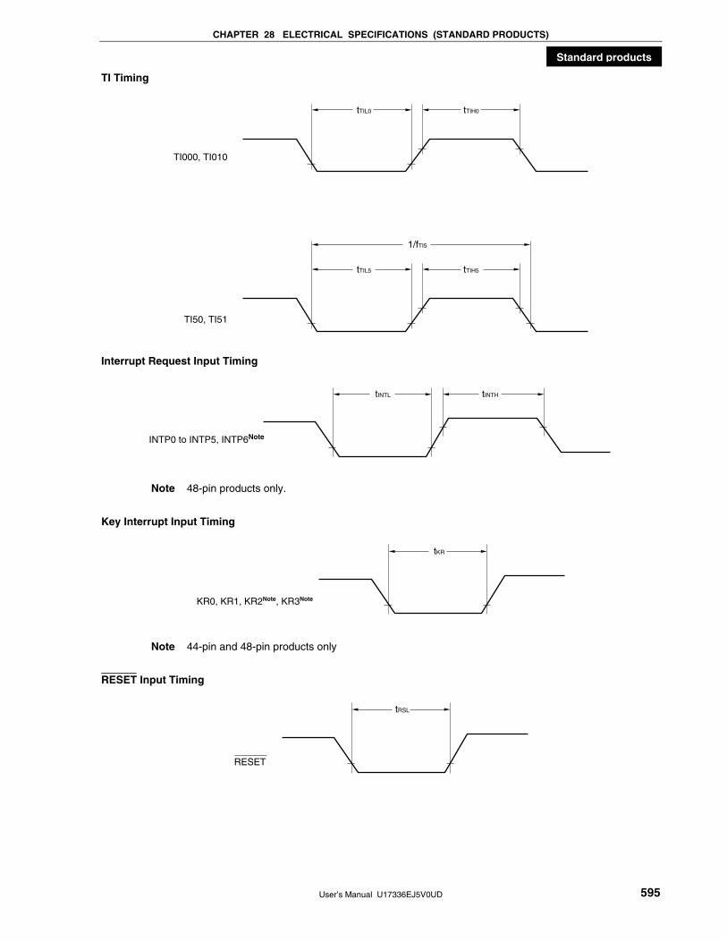
CHAPTER 28 ELECTRICAL SPECIFICATIONS (STANDARD PRODUCTS)
User’s Manual U17336EJ5V0UD 595
Standard products
TI Timing
TI000, TI010
tTIL0 tTIH0
TI50, TI51
1/fTI5
tTIL5 tTIH5
Interrupt Request Input Timing
INTP0 to INTP5, INTP6Note
tINTL tINTH
Note 48-pin products only.
Key Interrupt Input Timing
tKR
KR0, KR1, KR2Note, KR3Note
Note 44-pin and 48-pin products only
RESET Input Timing
RESET
tRSL

CHAPTER 28 ELECTRICAL SPECIFICATIONS (STANDARD PRODUCTS)
User’s Manual U17336EJ5V0UD 596
Standard products
(2) Serial interface
(TA = −40 to +85°C, 1.8 V ≤ VDD ≤ 5.5 V, AVREF ≤ VDD, VSS = AVSS = 0 V)
(a) UART6 (dedicated baud rate generator output)
Parameter Symbol Conditions MIN. TYP. MAX. Unit
Transfer rate 625 kbps
(b) UART0 (dedicated baud rate generator output)
Parameter Symbol Conditions MIN. TYP. MAX. Unit
Transfer rate 625 kbps
(c) IIC0
Standard Mode High-Speed Mode Parameter Symbol Conditions
MIN. MAX. MIN. MAX.
Unit
SCL0 clock frequency fSCL 0 100 0 400 kHz
Setup time of restart condition tSU: STA 4.7 − 0.6 − μs
Hold timeNote 1 tHD: STA 4.0 − 0.6 − μs
Internal clock operation 4.7 − 1.3 − μs Hold time when SCL0 = “L” tLOW
EXSCL0 clock (6.4 MHz)
operation
4.7 − 1.25 − μs
Hold time when SCL0 = “H” tHIGH 4.0 − 0.6 − μs
Data setup time (reception) tSU: DAT 250 − 100 − ns
0.9Note 4 DFC0 = 0 0 3.45 0
1.00Note 5
μs
0.9Note 6
fW = fXH/2N or fW =
fEXSCL0 selectedNote 3
DFC0 = 1 − − 0
1.125Note 7
μs
DFC0 = 0 0 3.45 0 1.05 μs
Data hold time (transmission)Note 2 tHD: DAT
fW = fRH/2N
selectedNote 3 DFC0 = 1 − − 0 1.184 μs
Setup time of stop condition tSU: STO 4.0 − 0.6 − μs
Bus free time tBUF 4.7 − 1.3 − μs
Notes 1. The first clock pulse is generated after this period when the start/restart condition is detected.
2. The maximum value (MAX.) of tHD:DAT is during normal transfer and a wait state is inserted in the ACK
(acknowledge) timing.
3. fW indicates the IIC0 transfer clock selected by the IICCL and IICX0 registers.
4. When fW ≥ 4.4 MHz is selected
5. When fW < 4.4 MHz is selected
6. When fW ≥ 5 MHz is selected
7. When fW < 5 MHz is selected
<R>

CHAPTER 28 ELECTRICAL SPECIFICATIONS (STANDARD PRODUCTS)
User’s Manual U17336EJ5V0UD 597
Standard products
(d) CSI10 (master mode, SCK10... internal clock output)
Parameter Symbol Conditions MIN. TYP. MAX. Unit
4.0 V ≤ VDD ≤ 5.5 V 160 ns
2.7 V ≤ VDD < 4.0 V 250 ns
SCK10 cycle time tKCY1
1.8 V ≤ VDD < 2.7 V 500 ns
4.0 V ≤ VDD ≤ 5.5 V tKCY1/2 − 15Note 1 ns
2.7 V ≤ VDD < 4.0 V tKCY1/2 − 25Note 1 ns
SCK10 high-/low-level width tKH1,
tKL1
1.8 V ≤ VDD < 2.7 V tKCY1/2 − 50Note 1 ns
4.0 V ≤ VDD ≤ 5.5 V 55 ns
2.7 V ≤ VDD < 4.0 V 80 ns
SI10 setup time (to SCK10↑) tSIK1
1.8 V ≤ VDD < 2.7 V 170 ns
SI10 hold time (from SCK10↑) tKSI1 30 ns
Delay time from SCK10↓ to
SO10 output
tKSO1 C = 50 pFNote 2 40 ns
Notes 1. This value is when high-speed system clock (fXH) is used.
2. C is the load capacitance of the SCK10 and SO10 output lines.
(e) CSI10 (slave mode, SCK10... external clock input)
Parameter Symbol Conditions MIN. TYP. MAX. Unit
SCK10 cycle time tKCY2 400 ns
SCK10 high-/low-level width tKH2,
tKL2
tKCY2/2 ns
SI10 setup time (to SCK10↑) tSIK2 80 ns
SI10 hold time (from SCK10↑) tKSI2 50 ns
4.0 V ≤ VDD ≤ 5.5 V 120 ns
2.7 V ≤ VDD < 4.0 V 120 ns
Delay time from SCK10↓ to
SO10 output
tKSO2 C = 50 pFNote
1.8 V ≤ VDD < 2.7 V 165 ns
Note C is the load capacitance of the SO10 output line.
<R>
<R>

CHAPTER 28 ELECTRICAL SPECIFICATIONS (STANDARD PRODUCTS)
User’s Manual U17336EJ5V0UD 598
Standard products
Serial Transfer Timing
IIC0:
tLOW
tHIGH
tHD: STA
Stopcondition
Startcondition
Restartcondition
Stopcondition
tSU: DAT
tSU: STA tHD: STAtHD: DAT
SCL0
SDA0
tBUF
tSU: STO
CSI10:
SI10
SO10

CHAPTER 28 ELECTRICAL SPECIFICATIONS (STANDARD PRODUCTS)
User’s Manual U17336EJ5V0UD 599
Standard products
A/D Converter Characteristics
(TA = −40 to +85°C, 2.3 V ≤ AVREF ≤ VDD ≤ 5.5 V, VSS = AVSS = 0 V)
Parameter Symbol Conditions MIN. TYP. MAX. Unit
Resolution RES 10 bit
4.0 V ≤ AVREF ≤ 5.5 V ±0.4 %FSR
2.7 V ≤ AVREF < 4.0 V ±0.6 %FSR
Overall errorNotes 1, 2 AINL
2.3 V ≤ AVREF < 2.7 V ±1.2 %FSR
4.0 V ≤ AVREF ≤ 5.5 V 6.1 36.7 μs
2.7 V ≤ AVREF < 4.0 V 12.2 36.7 μs
Conversion time tCONV
2.3 V ≤ AVREF < 2.7 V 27 66.6 μs
4.0 V ≤ AVREF ≤ 5.5 V ±0.4 %FSR
2.7 V ≤ AVREF < 4.0 V ±0.6 %FSR
Zero-scale errorNotes 1, 2 EZS
2.3 V ≤ AVREF < 2.7 V ±0.6 %FSR
4.0 V ≤ AVREF ≤ 5.5 V ±0.4 %FSR
2.7 V ≤ AVREF < 4.0 V ±0.6 %FSR
Full-scale errorNotes 1, 2 EFS
2.3 V ≤ AVREF < 2.7 V ±0.6 %FSR
4.0 V ≤ AVREF ≤ 5.5 V ±2.5 LSB
2.7 V ≤ AVREF < 4.0 V ±4.5 LSB
Integral non-linearity errorNote 1 ILE
2.3 V ≤ AVREF < 2.7 V ±6.5 LSB
4.0 V ≤ AVREF ≤ 5.5 V ±1.5 LSB
2.7 V ≤ AVREF < 4.0 V ±2.0 LSB
Differential non-linearity error Note 1 DLE
2.3 V ≤ AVREF < 2.7 V ±2.0 LSB
Analog input voltage VAIN AVSS AVREF V
Notes 1. Excludes quantization error (±1/2 LSB).
2. This value is indicated as a ratio (%FSR) to the full-scale value.
1.59 V POC Circuit Characteristics (TA = −40 to +85°C, VSS = 0 V)
Parameter Symbol Conditions MIN. TYP. MAX. Unit
Detection voltage VPOC 1.44 1.59 1.74 V
Power voltage rise inclination tPTH VDD: 0 V → change inclination of VPOC 0.5 V/ms
Minimum pulse width tPW 200 μs
POC Circuit Timing
Supply voltage(VDD)
Time
Detection voltage (MIN.)
Detection voltage (TYP.)
Detection voltage (MAX.)
tPTH
tPW

CHAPTER 28 ELECTRICAL SPECIFICATIONS (STANDARD PRODUCTS)
User’s Manual U17336EJ5V0UD 600
Standard products
Supply Voltage Rise Time (TA = −40 to +85°C, VSS = 0 V)
Parameter Symbol Conditions MIN. TYP. MAX. Unit
Maximum time to rise to 1.8 V (VDD (MIN.))
(VDD: 0 V → 1.8 V)
tPUP1 POCMODE (option byte) = 0,
when RESET input is not used
3.6 ms
Maximum time to rise to 1.8 V (VDD (MIN.))
(releasing RESET input → VDD: 1.8 V)
tPUP2 POCMODE (option byte) = 0,
when RESET input is used
1.9 ms
Supply Voltage Rise Time Timing
• When RESET pin input is not used • When RESET pin input is used
Supply voltage
(VDD)
Time
1.8 V
tPUP1
Supply voltage
(VDD)
Time
1.8 V
tPUP2
VPOC
RESET pin
2.7 V POC Circuit Characteristics (TA = −40 to +85°C, VSS = 0 V)
Parameter Symbol Conditions MIN. TYP. MAX. Unit
Detection voltage on application of supply
voltage
VDDPOC POCMODE (option byte) = 1 2.50 2.70 2.90 V

CHAPTER 28 ELECTRICAL SPECIFICATIONS (STANDARD PRODUCTS)
User’s Manual U17336EJ5V0UD 601
Standard products
LVI Circuit Characteristics (TA = −40 to +85°C, VPOC ≤ VDD ≤ 5.5 V, AVREF ≤ VDD, VSS = 0 V)
Parameter Symbol Conditions MIN. TYP. MAX. Unit
VLVI0 4.14 4.24 4.34 V
VLVI1 3.99 4.09 4.19 V
VLVI2 3.83 3.93 4.03 V
VLVI3 3.68 3.78 3.88 V
VLVI4 3.52 3.62 3.72 V
VLVI5 3.37 3.47 3.57 V
VLVI6 3.22 3.32 3.42 V
VLVI7 3.06 3.16 3.26 V
VLVI8 2.91 3.01 3.11 V
VLVI9 2.75 2.85 2.95 V
VLVI10 2.60 2.70 2.80 V
VLVI11 2.45 2.55 2.65 V
VLVI12 2.29 2.39 2.49 V
VLVI13 2.14 2.24 2.34 V
VLVI14 1.98 2.08 2.18 V
Supply voltage level
VLVI15 1.83 1.93 2.03 V
Detection
voltage
External input pinNote 1 EXLVI EXLVI < VDD, 1.8 V ≤ VDD ≤ 5.5 V 1.11 1.21 1.31 V
Minimum pulse width tLW 200 μs
Operation stabilization wait timeNote 2 tLWAIT 10 μs
Notes 1. The EXLVI/P120/INTP0 pin is used.
2. Time required from setting bit 7 (LVION) of the low-voltage detection register (LVIM) to 1 to operation
stabilization
Remark VLVI(n − 1) > VLVIn: n = 1 to 15
LVI Circuit Timing
Supply voltage
(VDD)
Time
Detection voltage (MIN.)
Detection voltage (TYP.)
Detection voltage (MAX.)
tLW
tLWAIT
LVION ← 1

CHAPTER 28 ELECTRICAL SPECIFICATIONS (STANDARD PRODUCTS)
User’s Manual U17336EJ5V0UD 602
Standard products
Data Memory STOP Mode Low Supply Voltage Data Retention Characteristics (TA = −40 to +85°C)
Parameter Symbol Conditions MIN. TYP. MAX. Unit
Data retention supply voltage VDDDR 1.44Note 5.5 V
Note The value depends on the POC detection voltage. When the voltage drops, the data is retained until a POC
reset is effected, but data is not retained when a POC reset is effected.
VDD
STOP instruction execution
Standby release signal(interrupt request)
STOP mode
Data retention mode
VDDDR
Operation mode
Flash Memory Programming Characteristics
(TA = −40 to +85°C, 2.7 V ≤ VDD ≤ 5.5 V, AVREF ≤ VDD, VSS = AVSS = 0 V)
• Basic characteristics
Parameter Symbol Conditions MIN. TYP. MAX. Unit
VDD supply current IDD fXP = 10 MHz (TYP.), 20 MHz (MAX.) 4.5 11.0 mA
All block Teraca 20 200 ms Erase timeNotes 1, 2
Block unit Terasa 20 200 ms
Write time (in 8-bit units)Note 1 Twrwa 10 100 μs
Number of rewrites per chip Cerwr Retention: 10 years
1 erase + 1 write after erase = 1 rewriteNote 3
100 Times
Notes 1. Characteristic of the flash memory. For the characteristic when a dedicated flash memory programmer,
PG-FP4, is used and the rewrite time during self programming, see Tables 25-12 and 25-13.
2. The prewrite time before erasure and the erase verify time (writeback time) are not included.
3. When a product is first written after shipment, “erase → write” and “write only” are both taken as one
rewrite.
Remarks 1. fXP: Main system clock oscillation frequency
2. For serial write operation characteristics, refer to 78K0/Kx2 Flash Memory Programming
(Programmer) Application Note (U17739E).
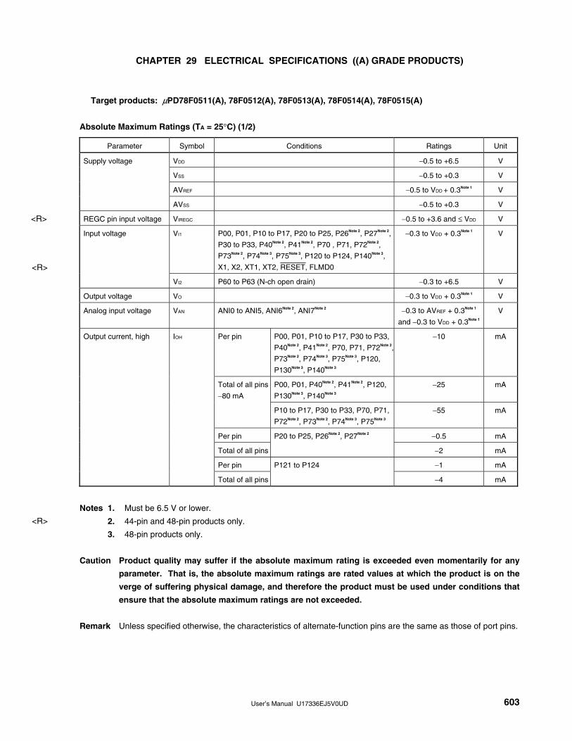
User’s Manual U17336EJ5V0UD 603
CHAPTER 29 ELECTRICAL SPECIFICATIONS ((A) GRADE PRODUCTS)
Target products: μPD78F0511(A), 78F0512(A), 78F0513(A), 78F0514(A), 78F0515(A)
Absolute Maximum Ratings (TA = 25°C) (1/2)
Parameter Symbol Conditions Ratings Unit
VDD −0.5 to +6.5 V
VSS −0.5 to +0.3 V
AVREF −0.5 to VDD + 0.3Note 1 V
Supply voltage
AVSS −0.5 to +0.3 V
REGC pin input voltage VIREGC −0.5 to +3.6 and ≤ VDD V
VI1 P00, P01, P10 to P17, P20 to P25, P26Note 2, P27Note 2,
P30 to P33, P40Note 2, P41Note 2, P70 , P71, P72Note 2,
P73Note 2, P74Note 3, P75Note 3, P120 to P124, P140Note 3,
X1, X2, XT1, XT2, RESET, FLMD0
−0.3 to VDD + 0.3Note 1 V Input voltage
VI2 P60 to P63 (N-ch open drain) −0.3 to +6.5 V
Output voltage VO −0.3 to VDD + 0.3Note 1 V
Analog input voltage VAN ANI0 to ANI5, ANI6Note 2, ANI7Note 2 −0.3 to AVREF + 0.3Note 1
and −0.3 to VDD + 0.3Note 1
V
Per pin P00, P01, P10 to P17, P30 to P33,
P40Note 2, P41Note 2, P70, P71, P72Note 2,
P73Note 2, P74Note 3, P75Note 3, P120,
P130Note 3, P140Note 3
−10 mA
P00, P01, P40Note 2, P41Note 2, P120,
P130Note 3, P140Note 3
−25 mA Total of all pins
−80 mA
P10 to P17, P30 to P33, P70, P71,
P72Note 2, P73Note 2, P74Note 3, P75Note 3
−55 mA
Per pin −0.5 mA
Total of all pins
P20 to P25, P26Note 2, P27Note 2
−2 mA
Per pin −1 mA
Output current, high IOH
Total of all pins
P121 to P124
−4 mA
Notes 1. Must be 6.5 V or lower.
2. 44-pin and 48-pin products only.
3. 48-pin products only.
Caution Product quality may suffer if the absolute maximum rating is exceeded even momentarily for any
parameter. That is, the absolute maximum ratings are rated values at which the product is on the
verge of suffering physical damage, and therefore the product must be used under conditions that
ensure that the absolute maximum ratings are not exceeded.
Remark Unless specified otherwise, the characteristics of alternate-function pins are the same as those of port pins.
<R>
<R>
<R>

CHAPTER 29 ELECTRICAL SPECIFICATIONS ((A) GRADE PRODUCTS)
User’s Manual U17336EJ5V0UD 604
(A) grade products
Absolute Maximum Ratings (TA = 25°C) (2/2)
Parameter Symbol Conditions Ratings Unit
Per pin P00, P01, P10 to P17, P30 to P33,
P40Note 1, P41Note 1, P60 to P63, P70,
P71, P72Note 1, P73Note 1, P74Note 2,
P75Note 2, P120, P130Note 2, P140Note 2
30 mA
P00, P01, P40Note 1, P41Note 1, P120,
P130Note 2, P140Note 2
60 mA Total of all pins
200 mA
P10 to P17, P30 to P33, P60 to
P63, P70, P71, P72Note 1, P73Note 1,
P74Note 2, P75Note 2
140 mA
Per pin 1 mA
Total of all pins
P20 to P25, P26Note 1, P27Note 1
5 mA
Per pin 4 mA
Output current, low IOL
Total of all pins
P121 to P124
10 mA
Operating ambient
temperature
TA −40 to +85 °C
Storage temperature Tstg −65 to +150 °C
Notes 1. 44-pin and 48-pin products only.
2. 48-pin products only.
Caution Product quality may suffer if the absolute maximum rating is exceeded even momentarily for any
parameter. That is, the absolute maximum ratings are rated values at which the product is on the
verge of suffering physical damage, and therefore the product must be used under conditions that
ensure that the absolute maximum ratings are not exceeded.
Remark Unless specified otherwise, the characteristics of alternate-function pins are the same as those of port pins.
<R>

CHAPTER 29 ELECTRICAL SPECIFICATIONS ((A) GRADE PRODUCTS)
User’s Manual U17336EJ5V0UD 605
(A) grade products
X1 Oscillator Characteristics
(TA = −40 to +85°C, 1.8 V ≤ VDD ≤ 5.5 V, VSS = AVSS = 0 V)
Resonator Recommended Circuit Parameter Conditions MIN. TYP. MAX. Unit
4.0 V ≤ VDD ≤ 5.5 V 1.0Note 2 20.0
2.7 V ≤ VDD < 4.0 V 1.0Note 2 10.0
Ceramic
resonator
C1
X2X1VSS
C2
X1 clock
oscillation
frequency (fX)Note 1
1.8 V ≤ VDD < 2.7 V 1.0 5.0
MHz
4.0 V ≤ VDD ≤ 5.5 V 1.0Note 2 20.0
2.7 V ≤ VDD < 4.0 V 1.0Note 2 10.0
Crystal
resonator
C1
X2X1VSS
C2
X1 clock
oscillation
frequency (fX)Note 1
1.8 V ≤ VDD < 2.7 V 1.0 5.0
MHz
Notes 1. Indicates only oscillator characteristics. Refer to AC Characteristics for instruction execution time.
2. 2.0 MHz (MIN.) when using UART6 during on-board programming.
Cautions 1. When using the X1 oscillator, wire as follows in the area enclosed by the broken lines in the
above figures to avoid an adverse effect from wiring capacitance.
• Keep the wiring length as short as possible.
• Do not cross the wiring with the other signal lines.
• Do not route the wiring near a signal line through which a high fluctuating current flows.
• Always make the ground point of the oscillator capacitor the same potential as VSS.
• Do not ground the capacitor to a ground pattern through which a high current flows.
• Do not fetch signals from the oscillator.
2. Since the CPU is started by the internal high-speed oscillation clock after a reset release, check
the X1 clock oscillation stabilization time using the oscillation stabilization time counter status
register (OSTC) by the user. Determine the oscillation stabilization time of the OSTC register
and oscillation stabilization time select register (OSTS) after sufficiently evaluating the
oscillation stabilization time with the resonator to be used.
Remark For the resonator selection and oscillator constant, customers are requested to either evaluate the
oscillation themselves or apply to the resonator manufacturer for evaluation.
<R>

CHAPTER 29 ELECTRICAL SPECIFICATIONS ((A) GRADE PRODUCTS)
User’s Manual U17336EJ5V0UD 606
(A) grade products
Internal Oscillator Characteristics
(TA = −40 to +85°C, 1.8 V ≤ VDD ≤ 5.5 V, VSS = AVSS = 0 V)
Resonator Parameter Conditions MIN. TYP. MAX. Unit
2.7 V ≤ VDD ≤ 5.5 V 7.6 8.0 8.4 MHz RSTS = 1
1.8 V ≤ VDD < 2.7 V 7.6 8.0 10.4 MHz
8 MHz internal oscillator Internal high-speed oscillation
clock frequency (fRH)Note
RSTS = 0 2.48 5.6 9.86 MHz
2.7 V ≤ VDD ≤ 5.5 V 216 240 264 kHz 240 kHz internal oscillator Internal low-speed oscillation
clock frequency (fRL) 1.8 V ≤ VDD < 2.7 V 192 240 264 kHz
Note Indicates only oscillator characteristics. Refer to AC Characteristics for instruction execution time.
Remark RSTS: Bit 7 of the internal oscillation mode register (RCM)
XT1 Oscillator Characteristics
(TA = −40 to +85°C, 1.8 V ≤ VDD ≤ 5.5 V, VSS = AVSS = 0 V)
Resonator Recommended Circuit Parameter Conditions MIN. TYP. MAX. Unit
Crystal
resonator
XT1VSS XT2
C4 C3
Rd
XT1 clock oscillation
frequency (fXT)Note
32 32.768 35 kHz
Note Indicates only oscillator characteristics. Refer to AC Characteristics for instruction execution time.
Cautions 1. When using the XT1 oscillator, wire as follows in the area enclosed by the broken lines in the
above figure to avoid an adverse effect from wiring capacitance.
• Keep the wiring length as short as possible.
• Do not cross the wiring with the other signal lines.
• Do not route the wiring near a signal line through which a high fluctuating current flows.
• Always make the ground point of the oscillator capacitor the same potential as VSS.
• Do not ground the capacitor to a ground pattern through which a high current flows.
• Do not fetch signals from the oscillator.
2. The XT1 oscillator is designed as a low-amplitude circuit for reducing power consumption, and
is more prone to malfunction due to noise than the X1 oscillator. Particular care is therefore
required with the wiring method when the XT1 clock is used.
Remark For the resonator selection and oscillator constant, customers are requested to either evaluate the
oscillation themselves or apply to the resonator manufacturer for evaluation.
<R>

CHAPTER 29 ELECTRICAL SPECIFICATIONS ((A) GRADE PRODUCTS)
User’s Manual U17336EJ5V0UD 607
(A) grade products
DC Characteristics (1/5)
(TA = −40 to +85°C, 1.8 V ≤ VDD ≤ 5.5 V, AVREF ≤ VDD, VSS = AVSS = 0 V)
Parameter Symbol Conditions MIN. TYP. MAX. Unit
4.0 V ≤ VDD ≤ 5.5 V −3.0 mA
2.7 V ≤ VDD < 4.0 V −2.5 mA
Per pin for P00, P01, P10 to P17, P30 to P33, P40Note 2, P41Note 2, P70, P71, P72Note 2, P73Note 2, P74Note 3, P75Note 3, P120, P130Note 3, P140Note 3
1.8 V ≤ VDD < 2.7 V −1.0 mA
4.0 V ≤ VDD ≤ 5.5 V −12.0 mA
2.7 V ≤ VDD < 4.0 V −7.0 mA
Total of pinsNote 5 P00, P01, P40Note 2, P41Note 2, P120, P130Note 3, P140Note 3
1.8 V ≤ VDD < 2.7 V −5.0 mA
4.0 V ≤ VDD ≤ 5.5 V −18.0 mA
2.7 V ≤ VDD < 4.0 V −15.0 mA
Total of pinsNote 5 P10 to P17, P30 to P33, P70, P71, P72Note 2, P73Note 2, P74Note 3, P75Note 3
1.8 V ≤ VDD < 2.7 V −10.0 mA
4.0 V ≤ VDD ≤ 5.5 V −23.0 mA
2.7 V ≤ VDD < 4.0 V −20.0 mA
IOH1
Total of all pinsNote 5
1.8 V ≤ VDD < 2.7 V −15.0 mA
Per pin for P20 to P25, P26Note 2, P27Note 2 AVREF = VDD −0.1 mA
Output current, highNote 1
IOH2
Per pin for P121 to P124 −0.1 mA
4.0 V ≤ VDD ≤ 5.5 V 8.5 mA
2.7 V ≤ VDD < 4.0 V 5.0 mA
Per pin for P00, P01, P10 to P17, P30 to P33, P40Note 2, P41Note 2, P70, P71, P72Note 2, P73Note 2, P74Note 3, P75Note 3, P120, P130Note 3, P140Note 3
1.8 V ≤ VDD < 2.7 V 2.0 mA
4.0 V ≤ VDD ≤ 5.5 V 15.0 mA
2.7 V ≤ VDD < 4.0 V 5.0 mA
Per pin for P60 to P63
1.8 V ≤ VDD < 2.7 V 2.0 mA
4.0 V ≤ VDD ≤ 5.5 V 20.0 mA
2.7 V ≤ VDD < 4.0 V 15.0 mA
Total of pinsNote 5 P00, P01, P40Note 2, P41Note 2, P120, P130Note 3, P140Note 3
1.8 V ≤ VDD < 2.7 V 9.0 mA
4.0 V ≤ VDD ≤ 5.5 V 45.0 mA
2.7 V ≤ VDD < 4.0 V 35.0 mA
Total of pinsNote 5 P10 to P17, P30 to P33, P60 to P63, P70, P71, P72Note 2, P73Note 2, P74Note 3, P75Note 3
1.8 V ≤ VDD < 2.7 V 20.0 mA
4.0 V ≤ VDD ≤ 5.5 V 65.0 mA
2.7 V ≤ VDD < 4.0 V 50.0 mA
Output current, lowNote 4
IOL1
Total of all pinsNote 5
1.8 V ≤ VDD < 2.7 V 29.0 mA
Notes 1. Value of current at which the device operation is guaranteed even if the current flows from VDD to an output
pin.
2. 44-pin and 48-pin products only.
3. 48-pin products only.
4. Value of current at which the device operation is guaranteed even if the current flows from an output pin to
GND.
5. Specification under conditions where the duty factor is 70% (time for which current is output is 0.7 × t and
time for which current is not output is 0.3 × t, where t is a specific time). The total output current of the pins
at a duty factor of other than 70% can be calculated by the following expression.
• Where the duty factor of IOH is n%: Total output current of pins = (IOH × 0.7)/(n × 0.01)
<Example> Where the duty factor is 50%, IOH = 20.0 mA
Total output current of pins = (20.0 × 0.7)/(50 × 0.01) = 28.0 mA
However, the current that is allowed to flow into one pin does not vary depending on the duty factor. A
current higher than the absolute maximum rating must not flow into one pin.
Remark Unless specified otherwise, the characteristics of alternate-function pins are the same as those of port pins.

CHAPTER 29 ELECTRICAL SPECIFICATIONS ((A) GRADE PRODUCTS)
User’s Manual U17336EJ5V0UD 608
(A) grade products
DC Characteristics (2/5)
(TA = −40 to +85°C, 1.8 V ≤ VDD ≤ 5.5 V, AVREF ≤ VDD, VSS = AVSS = 0 V)
Parameter Symbol Conditions MIN. TYP. MAX. Unit
Per pin for P20 to P25, P26Note 2,
P27Note 2
AVREF = VDD 0.4 mA Output current, lowNote 1 IOL2
Per pin for P121 to P124 0.4 mA
VIH1 P12, P13, P15, P40Note 2, P41Note 2, P121 to P124 0.7VDD VDD V
VIH2 P00, P01, P10, P11, P14, P16, P17, P30 to P33, P70,
P71, P72Note 2, P73Note 2, P74Note 3, P75Note 3, P120,
P140Note 3, RESET, EXCLK, EXCLKS
0.8VDD VDD V
VIH3 P20 to P25, P26Note 2, P27Note 2 AVREF = VDD 0.7AVREF AVREF V
Input voltage, high
VIH4 P60 to P63 0.7VDD 6.0 V
VIL1 P12, P13, P15, P40, P41, P60 to P63, P121 to P124 0 0.3VDD V
VIL2 P00, P01, P10, P11, P14, P16, P17, P30 to P33,
P70 to P73, P74Note 2, P75Note 2, P120, P140Note 2, RESET,
EXCLK, EXCLKS
0 0.2VDD V
Input voltage, low
VIL3 P20 to P25, P26Note 2, P27Note 2 AVREF = VDD 0 0.3AVREF V
4.0 V ≤ VDD ≤ 5.5 V,
IOH1 = −3.0 mA
VDD − 0.7 V
2.7 V ≤ VDD < 4.0 V,
IOH1 = −2.5 mA
VDD − 0.5 V
VOH1 P00, P01, P10 to P17,
P30 to P33, P40Note 2, P41Note 2,
P70, P71, P72Note 2, P73Note 2,
P74Note 3, P75Note 3, P120, P130Note 3,
P140Note 3 1.8 V ≤ VDD < 2.7 V,
IOH1 = −1.0 mA
VDD − 0.5 V
P20 to P25, P26Note 2, P27Note 2 AVREF = VDD,
IOH2 = −100 μA
VDD − 0.5 V
Output voltage, high
VOH2
P121 to P124 IOH2 = −100 μA VDD − 0.5 V
Notes 1. Value of current at which the device operation is guaranteed
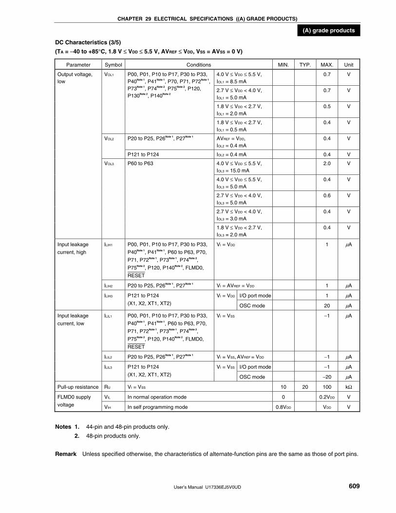
CHAPTER 29 ELECTRICAL SPECIFICATIONS ((A) GRADE PRODUCTS)
User’s Manual U17336EJ5V0UD 609
(A) grade products
DC Characteristics (3/5)
(TA = −40 to +85°C, 1.8 V ≤ VDD ≤ 5.5 V, AVREF ≤ VDD, VSS = AVSS = 0 V)
Parameter Symbol Conditions MIN. TYP. MAX. Unit
4.0 V ≤ VDD ≤ 5.5 V, IOL1 = 8.5 mA
0.7 V
2.7 V ≤ VDD < 4.0 V, IOL1 = 5.0 mA
0.7 V
1.8 V ≤ VDD < 2.7 V, IOL1 = 2.0 mA
0.5 V
VOL1 P00, P01, P10 to P17, P30 to P33, P40Note 1, P41Note 1, P70, P71, P72Note 1, P73Note 1, P74Note 2, P75Note 2, P120, P130Note 2, P140Note 2
1.8 V ≤ VDD < 2.7 V, IOL1 = 0.5 mA
0.4 V
P20 to P25, P26Note 1, P27Note 1 AVREF = VDD, IOL2 = 0.4 mA
0.4 V VOL2
P121 to P124 IOL2 = 0.4 mA 0.4 V
4.0 V ≤ VDD ≤ 5.5 V, IOL3 = 15.0 mA
2.0 V
4.0 V ≤ VDD ≤ 5.5 V, IOL3 = 5.0 mA
0.4 V
2.7 V ≤ VDD < 4.0 V, IOL3 = 5.0 mA
0.6 V
2.7 V ≤ VDD < 4.0 V, IOL3 = 3.0 mA
0.4 V
Output voltage, low
VOL3 P60 to P63
1.8 V ≤ VDD < 2.7 V, IOL3 = 2.0 mA
0.4 V
ILIH1 P00, P01, P10 to P17, P30 to P33,
P40Note 1, P41Note 1, P60 to P63, P70,
P71, P72Note 1, P73Note 1, P74Note 2,
P75Note 2, P120, P140Note 2, FLMD0,
RESET
VI = VDD 1 μA
ILIH2 P20 to P25, P26Note 1, P27Note 1 VI = AVREF = VDD 1 μA
I/O port mode 1 μA
Input leakage
current, high
ILIH3 P121 to P124
(X1, X2, XT1, XT2)
VI = VDD
OSC mode 20 μA
ILIL1 P00, P01, P10 to P17, P30 to P33,
P40Note 1, P41Note 1, P60 to P63, P70,
P71, P72Note 1, P73Note 1, P74Note 2,
P75Note 2, P120, P140Note 2, FLMD0,
RESET
VI = VSS −1 μA
ILIL2 P20 to P25, P26Note 1, P27Note 1 VI = VSS, AVREF = VDD −1 μA
I/O port mode −1 μA
Input leakage
current, low
ILIL3 P121 to P124
(X1, X2, XT1, XT2)
VI = VSS
OSC mode −20 μA
Pull-up resistance RU VI = VSS 10 20 100 kΩ
VIL In normal operation mode 0 0.2VDD V FLMD0 supply
voltage VIH In self programming mode 0.8VDD VDD V
Notes 1. 44-pin and 48-pin products only.
2. 48-pin products only.
Remark Unless specified otherwise, the characteristics of alternate-function pins are the same as those of port pins.

CHAPTER 29 ELECTRICAL SPECIFICATIONS ((A) GRADE PRODUCTS)
User’s Manual U17336EJ5V0UD 610
(A) grade products
DC Characteristics (4/5)
(TA = −40 to +85°C, 1.8 V ≤ VDD ≤ 5.5 V, AVREF ≤ VDD, VSS = AVSS = 0 V)
Parameter Symbol Conditions MIN. TYP. MAX. Unit
Square wave input 3.2 5.5 fXH = 20 MHzNote 2,
VDD = 5.0 V Resonator connection 4.5 6.9
mA
Square wave input 1.6 2.8 fXH = 10 MHzNotes 2, 3,
VDD = 5.0 V Resonator connection 2.3 3.9
mA
Square wave input 1.5 2.7 fXH = 10 MHzNotes 2, 3,
VDD = 3.0 V Resonator connection 2.2 3.2
mA
Square wave input 0.9 1.6 fXH = 5 MHzNotes 2, 3,
VDD = 3.0 V Resonator connection 1.3 2.0
mA
Square wave input 0.7 1.4 fXH = 5 MHzNotes 2, 3,
VDD = 2.0 V Resonator connection 1.0 1.6
mA
fRH = 8 MHzNote 4, VDD = 5.0 V 1.4 2.5 mA
Square wave input 6 30
IDD1 Operating
mode
fSUB = 32.768 kHzNote 5,
VDD = 5.0 V Resonator connection 15 35
μA
Square wave input 0.8 2.6 fXH = 20 MHzNote 2,
VDD = 5.0 V Resonator connection 2.0 4.4
mA
Square wave input 0.4 1.3 fXH = 10 MHzNotes 2, 3,
VDD = 5.0 V Resonator connection 1.0 2.4
mA
Square wave input 0.2 0.65 fXH = 5 MHzNotes 2, 3,
VDD = 3.0 V Resonator connection 0.5 1.1
mA
fRH = 8 MHzNote 4, VDD = 5.0 V 0.4 1.2 mA
Square wave input 3.0 27
IDD2 HALT mode
fSUB = 32.768 kHzNote 5,
VDD = 5.0 V Resonator connection 12 32
μA
VDD = 5.0 V 1 20 μA
Supply currentNote 1
IDD3 STOP modeNote 6
VDD = 5.0 V, TA = −40 to +70°C 1 10 μA
Notes 1. Total current flowing into the internal power supply (VDD), including the peripheral operation current and
the input leakage current flowing when the level of the input pin is fixed to VDD or VSS. However, the
current flowing into the pull-up resistors and the output current of the port are not included.
2. Not including the operating current of the 8 MHz internal oscillator, 240 kHz internal oscillator, and XT1
oscillator, and the current flowing into the A/D converter, watchdog timer and LVI circuit.
3. When AMPH (bit 0 of clock operation mode select register (OSCCTL)) = 0.
4. Not including the operating current of the X1 oscillator, XT1 oscillator, and 240 kHz internal oscillator, and
the current flowing into the A/D converter, watchdog timer and LVI circuit.
5. Not including the operating current of the X1 oscillator, 8 MHz internal oscillator, and 240 kHz internal
oscillator, and the current flowing into the A/D converter, watchdog timer and LVI circuit.
6. Not including the operating current of the 240 kHz internal oscillator and XT1 oscillator, and the current
flowing into the A/D converter, watchdog timer and LVI circuit.
Remarks 1. fXH: High-speed system clock frequency (X1 clock oscillation frequency or external main system clock
frequency)
2. fRH: Internal high-speed oscillation clock frequency
3. fSUB: Subsystem clock frequency (XT1 clock oscillation frequency or external subsystem clock
frequency)
<R>
<R>
<R>
<R>
<R>
<R>
<R>

CHAPTER 29 ELECTRICAL SPECIFICATIONS ((A) GRADE PRODUCTS)
User’s Manual U17336EJ5V0UD 611
(A) grade products
DC Characteristics (5/5)
(TA = −40 to +85°C, 1.8 V ≤ VDD ≤ 5.5 V, AVREF ≤ VDD, VSS = AVSS = 0 V)
Parameter Symbol Conditions MIN. TYP. MAX. Unit
A/D converter
operating current
IADCNote 1 2.3 V ≤ AVREF ≤ VDD, ADCE = 1 0.86 1.9 mA
Watchdog timer
operating current
IWDTNote 2 During 240 kHz internal low-speed oscillation clock
operation
5 10 μA
LVI operating current ILVINote 3 9 18 μA
Notes 1. Current flowing only to the A/D converter (AVREF). The current value of the 78K0/KC2 is the sum of IDD1 or
IDD2 and IADC when the A/D converter operates in an operation mode or the HALT mode.
2. Current flowing only to the watchdog timer, including the operating current of the 240 kHz internal
oscillator. The current value of the 78K0/KC2 is the sum of IDD2 or IDD3 and IWDT when the watchdog timer
operates in the HALT or STOP mode.
3. Current flowing only to the LVI circuit. The current value of the 78K0/KC2 is the sum of IDD2 or IDD3 and ILVI
when the LVI circuit operates in the HALT or STOP mode.
<R>
<R>

CHAPTER 29 ELECTRICAL SPECIFICATIONS ((A) GRADE PRODUCTS)
User’s Manual U17336EJ5V0UD 612
(A) grade products
AC Characteristics
(1) Basic operation
(TA = −40 to +85°C, 1.8 V ≤ VDD ≤ 5.5 V, AVREF ≤ VDD, VSS = AVSS = 0 V)
Parameter Symbol Conditions MIN. TYP. MAX. Unit
4.0 V ≤ VDD ≤ 5.5 V 0.1 32 μs
2.7 V ≤ VDD < 4.0 V 0.2 32 μs
Main system
clock (fXP)
operation 1.8 V ≤ VDD < 2.7 V 0.4Note 1 32 μs
Instruction cycle (minimum
instruction execution time)
TCY
Subsystem clock (fSUB) operation 114 122 125 μs
4.0 V ≤ VDD ≤ 5.5 V 20 MHz
2.7 V ≤ VDD < 4.0 V 10 MHz
fPRS = fXH
(XSEL = 1)
1.8 V ≤ VDD < 2.7 V 5 MHz
2.7 V ≤ VDD < 5.5 V 7.6 8.4 MHz
Peripheral hardware clock
frequency
fPRS
fPRS = fRH
(XSEL = 0) 1.8 V ≤ VDD < 2.7 VNote 2 7.6 10.4 MHz
4.0 V ≤ VDD ≤ 5.5 V 1.0Note 3 20.0 MHz
2.7 V ≤ VDD < 4.0 V 1.0Note 3 10.0 MHz
External main system clock
frequency
fEXCLK
1.8 V ≤ VDD < 2.7 V 1.0 5.0 MHz
4.0 V ≤ VDD ≤ 5.5 V 24 ns
2.7 V ≤ VDD < 4.0 V 48 ns
External main system clock input
high-level width, low-level width
tEXCLKH,
tEXCLKL
1.8 V ≤ VDD < 2.7 V 96 ns
External subsystem clock
frequency
fEXCLKS 32 32.768 35 kHz
External subsystem clock input
high-level width, low-level width
tEXCLKSH,
tEXCLKSL
12 μs
4.0 V ≤ VDD ≤ 5.5 V 2/fsam + 0.1Note 4 μs
2.7 V ≤ VDD < 4.0 V 2/fsam + 0.2Note 4 μs
TI000, TI010 input high-level
width, low-level width
tTIH0,
tTIL0
1.8 V ≤ VDD < 2.7 V 2/fsam + 0.5Note 4 μs
4.0 V ≤ VDD ≤ 5.5 V 10 MHz
2.7 V ≤ VDD < 4.0 V 10 MHz
TI50, TI51 input frequency fTI5
1.8 V ≤ VDD < 2.7 V 5 MHz
4.0 V ≤ VDD ≤ 5.5 V 50 ns
2.7 V ≤ VDD < 4.0 V 50 ns
TI50, TI51 input high-level width,
low-level width
tTIH5,
tTIL5
1.8 V ≤ VDD < 2.7 V 100 ns
Interrupt input high-level width,
low-level width
tINTH,
tINTL
1 μs
Key interrupt input low-level width tKR 250 ns
RESET low-level width tRSL 10 μs
Notes 1. 0.38 μs when operating with the 8 MHz internal oscillator.
2. Characteristics of the main system clock frequency. Set the division clock to be set by a peripheral
function to fRH/2 or less.
3. 2.0 MHz (MIN.) when using UART6 during on-board programming.
4. Selection of fsam = fPRS, fPRS/4, fPRS/256 is possible using bits 0 and 1 (PRM000, PRM001) of prescaler
mode register 00 (PRM00). Note that when selecting the TI000 valid edge as the count clock, fsam =
fPRS.
<R>
<R>
<R>
<R>
<R>

CHAPTER 29 ELECTRICAL SPECIFICATIONS ((A) GRADE PRODUCTS)
User’s Manual U17336EJ5V0UD 613
(A) grade products
TCY vs. VDD (Main System Clock Operation)
5.0
1.0
2.0
0.4
0.2
0.1
0
10
1.0 2.0 3.0 4.0 5.0 6.05.5
2.7
100
0.01
1.8
32
Supply voltage VDD [V]
Cyc
le ti
me
TC
Y [
s]
Guaranteed operation range
μ
AC Timing Test Points
VIH
VIL
Test pointsVIH
VIL
External Main System Clock Timing, External Subsystem Clock Timing
EXCLK0.8VDD (MIN.)
0.2VDD (MAX.)
1/fEXCLK
tEXCLKL tEXCLKH
1/fEXCLKS
tEXCLKSL tEXCLKSH
EXCLKS0.8VDD (MIN.)
0.2VDD (MAX.)

CHAPTER 29 ELECTRICAL SPECIFICATIONS ((A) GRADE PRODUCTS)
User’s Manual U17336EJ5V0UD 614
(A) grade products
TI Timing
TI000, TI010
tTIL0 tTIH0
TI50, TI51
1/fTI5
tTIL5 tTIH5
Interrupt Request Input Timing
INTP0 to INTP5, INTP6Note
tINTL tINTH
Note 48-pin products only.
Key Interrupt Input Timing
KR0, KR1, KR2Note, KR3Note
tKR
Note 44-pin and 48-pin products only
RESET Input Timing
RESET
tRSL

CHAPTER 29 ELECTRICAL SPECIFICATIONS ((A) GRADE PRODUCTS)
User’s Manual U17336EJ5V0UD 615
(A) grade products
(2) Serial interface
(TA = −40 to +85°C, 1.8 V ≤ VDD ≤ 5.5 V, AVREF ≤ VDD, VSS = AVSS = 0 V)
(a) UART6 (dedicated baud rate generator output)
Parameter Symbol Conditions MIN. TYP. MAX. Unit
Transfer rate 625 kbps
(b) UART0 (dedicated baud rate generator output)
Parameter Symbol Conditions MIN. TYP. MAX. Unit
Transfer rate 625 kbps
(c) IIC0
Standard Mode High-Speed ModeParameter Symbol Conditions
MIN. MAX. MIN. MAX.
Unit
SCL0 clock frequency fSCL 0 100 0 400 kHz
Setup time of restart condition tSU:STA 4.7 − 0.6 − μs
Hold timeNote 1 tHD:STA 4.0 − 0.6 − μs
Internal clock operation 4.7 − 1.3 − μs Hold time when SCL0 = “L” tLOW
EXSCL0 clock (6.4 MHz) operation 4.7 − 1.25 − μs
Hold time when SCL0 = “H” tHIGH 4.0 − 0.6 − μs
Data setup time (reception) tSU:DAT 250 − 100 − ns
0.9Note 4 DFC0 = 0 0 3.45 0
1.00Note 5
μs
0.9Note 6
fW = fXH/2N or
fW = fEXSCL0 selectedNote 3
DFC0 = 1 − − 0
1.125Note 7
μs
DFC0 = 0 0 3.45 0 1.05 μs
Data setup time
(transmission)Note 2
tHD:DAT
fW = fRH/2N selectedNote 3
DFC0 = 1 − − 0 1.184 μs
Setup time of stop condition tSU:STO 4.0 − 0.6 − μs
Bus free time tBUF 4.7 − 1.3 − μs
Notes 1. The first clock pulse is generated after this period when the start/restart condition is detected.
2. The maximum value (MAX.) of tHD:DAT is during normal transfer and a wait state is inserted in the ACK
(acknowledge) timing.
3. fW indicates the IIC0 transfer clock selected by the IICCL and IICX0 registers.
4. When fW ≥ 4.4 MHz is selected
5. When fW < 4.4 MHz is selected
6. When fW ≥ 5 MHz is selected
7. When fW < 5 MHz is selected
<R>
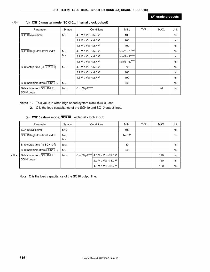
CHAPTER 29 ELECTRICAL SPECIFICATIONS ((A) GRADE PRODUCTS)
User’s Manual U17336EJ5V0UD 616
(A) grade products
(d) CSI10 (master mode, SCK10... internal clock output)
Parameter Symbol Conditions MIN. TYP. MAX. Unit
4.0 V ≤ VDD ≤ 5.5 V 100 ns
2.7 V ≤ VDD < 4.0 V 200 ns
SCK10 cycle time tKCY1
1.8 V ≤ VDD < 2.7 V 400 ns
4.0 V ≤ VDD ≤ 5.5 V tKCY1/2 − 20Note 1 ns
2.7 V ≤ VDD < 4.0 V tKCY1/2 − 30Note 1 ns
SCK10 high-/low-level width tKH1,
tKL1
1.8 V ≤ VDD < 2.7 V tKCY1/2 − 60Note 1 ns
4.0 V ≤ VDD ≤ 5.5 V 70 ns
2.7 V ≤ VDD < 4.0 V 100 ns
SI10 setup time (to SCK10↑) tSIK1
1.8 V ≤ VDD < 2.7 V 190 ns
SI10 hold time (from SCK10↑) tKSI1 30 ns
Delay time from SCK10↓ to
SO10 output
tKSO1 C = 50 pFNote 2 40 ns
Notes 1. This value is when high-speed system clock (fXH) is used.
2. C is the load capacitance of the SCK10 and SO10 output lines.
(e) CSI10 (slave mode, SCK10... external clock input)
Parameter Symbol Conditions MIN. TYP. MAX. Unit
SCK10 cycle time tKCY2 400 ns
SCK10 high-/low-level width tKH2,
tKL2
tKCY2/2 ns
SI10 setup time (to SCK10↑) tSIK2 80 ns
SI10 hold time (from SCK10↑) tKSI2 50 ns
4.0 V ≤ VDD ≤ 5.5 V 120 ns
2.7 V ≤ VDD < 4.0 V 120 ns
Delay time from SCK10↓ to
SO10 output
tKSO2 C = 50 pFNote
1.8 V ≤ VDD < 2.7 V 180 ns
Note C is the load capacitance of the SO10 output line.
<R>
<R>

CHAPTER 29 ELECTRICAL SPECIFICATIONS ((A) GRADE PRODUCTS)
User’s Manual U17336EJ5V0UD 617
(A) grade products
Serial Transfer Timing
IIC0:
tLOW
tHIGH
tHD:STA tSU:DAT
tSU:STA tHD:STAtHD:DAT
SCL0
SDA0
tBUF
tSU:STO
Stop condition
Start condition
Restart condition
Stop condition
CSI10:
SI10
SO10
tKCYm
tKLm tKHm
tSIKm tKSIm
Input data
tKSOm
Output data
SCK10
Remark m = 1, 2
<R>

CHAPTER 29 ELECTRICAL SPECIFICATIONS ((A) GRADE PRODUCTS)
User’s Manual U17336EJ5V0UD 618
(A) grade products
A/D Converter Characteristics
(TA = −40 to +85°C, 2.3 V ≤ AVREF ≤ VDD ≤ 5.5 V, VSS = AVSS = 0 V)
Parameter Symbol Conditions MIN. TYP. MAX. Unit
Resolution RES 10 bit
4.0 V ≤ AVREF ≤ 5.5 V ±0.4 %FSR
2.7 V ≤ AVREF < 4.0 V ±0.6 %FSR
Overall errorNotes 1, 2 AINL
2.3 V ≤ AVREF < 2.7 V ±1.2 %FSR
4.0 V ≤ AVREF ≤ 5.5 V 6.1 36.7 μs
2.7 V ≤ AVREF < 4.0 V 12.2 36.7 μs
Conversion time tCONV
2.3 V ≤ AVREF < 2.7 V 27 66.6 μs
4.0 V ≤ AVREF ≤ 5.5 V ±0.4 %FSR
2.7 V ≤ AVREF < 4.0 V ±0.6 %FSR
Zero-scale errorNotes 1, 2 EZS
2.3 V ≤ AVREF < 2.7 V ±0.6 %FSR
4.0 V ≤ AVREF ≤ 5.5 V ±0.4 %FSR
2.7 V ≤ AVREF < 4.0 V ±0.6 %FSR
Full-scale errorNotes 1, 2 EFS
2.3 V ≤ AVREF < 2.7 V ±0.6 %FSR
4.0 V ≤ AVREF ≤ 5.5 V ±2.5 LSB
2.7 V ≤ AVREF < 4.0 V ±4.5 LSB
Integral non-linearity errorNote 1 ILE
2.3 V ≤ AVREF < 2.7 V ±6.5 LSB
4.0 V ≤ AVREF ≤ 5.5 V ±1.5 LSB
2.7 V ≤ AVREF < 4.0 V ±2.0 LSB
Differential non-linearity errorNote 1 DLE
2.3 V ≤ AVREF < 2.7 V ±2.0 LSB
Analog input voltage VAIN AVSS AVREF V
Notes 1. Excludes quantization error (±1/2 LSB).
2. This value is indicated as a ratio (%FSR) to the full-scale value.
1.59 V POC Circuit Characteristics (TA = −40 to +85°C, VSS = 0 V)
Parameter Symbol Conditions MIN. TYP. MAX. Unit
Detection voltage VPOC 1.44 1.59 1.74 V
Power voltage rise inclination tPTH VDD: 0 V → change inclination of VPOC 0.5 V/ms
Minimum pulse width tPW 200 μs
POC Circuit Timing
Supply voltage(VDD)
Time
Detection voltage (MIN.)
Detection voltage (TYP.)
Detection voltage (MAX.)
tPTH
tPW

CHAPTER 29 ELECTRICAL SPECIFICATIONS ((A) GRADE PRODUCTS)
User’s Manual U17336EJ5V0UD 619
(A) grade products
Supply Voltage Rise Time (TA = −40 to +85°C, VSS = 0 V)
Parameter Symbol Conditions MIN. TYP. MAX. Unit
Maximum time to rise to 1.8 V (VDD (MIN.))
(VDD: 0 V → 1.8 V)
tPUP1 POCMODE (option byte) = 0,
when RESET input is not used
3.6 ms
Maximum time to rise to 1.8 V (VDD (MIN.))
(releasing RESET input → VDD: 1.8 V)
tPUP2 POCMODE (option byte) = 0,
when RESET input is used
1.9 ms
Supply Voltage Rise Time Timing
• When RESET pin input is not used • When RESET pin input is used
Supply voltage
(VDD)
Time
1.8 V
tPUP1
Supply voltage
(VDD)
Time
1.8 V
tPUP2
VPOC
RESET pin
2.7 V POC Circuit Characteristics (TA = −40 to +85°C, VSS = 0 V)
Parameter Symbol Conditions MIN. TYP. MAX. Unit
Detection voltage on application of supply
voltage
VDDPOC POCMODE (option byte) = 1 2.50 2.70 2.90 V

CHAPTER 29 ELECTRICAL SPECIFICATIONS ((A) GRADE PRODUCTS)
User’s Manual U17336EJ5V0UD 620
(A) grade products
LVI Circuit Characteristics (TA = −40 to +85°C, VPOC ≤ VDD ≤ 5.5 V, AVREF ≤ VDD, VSS = 0 V)
Parameter Symbol Conditions MIN. TYP. MAX. Unit
VLVI0 4.14 4.24 4.34 V
VLVI1 3.99 4.09 4.19 V
VLVI2 3.83 3.93 4.03 V
VLVI3 3.68 3.78 3.88 V
VLVI4 3.52 3.62 3.72 V
VLVI5 3.37 3.47 3.57 V
VLVI6 3.22 3.32 3.42 V
VLVI7 3.06 3.16 3.26 V
VLVI8 2.91 3.01 3.11 V
VLVI9 2.75 2.85 2.95 V
VLVI10 2.60 2.70 2.80 V
VLVI11 2.45 2.55 2.65 V
VLVI12 2.29 2.39 2.49 V
VLVI13 2.14 2.24 2.34 V
VLVI14 1.98 2.08 2.18 V
Supply voltage level
VLVI15 1.83 1.93 2.03 V
Detection
voltage
External input pinNote 1 EXLVI EXLVI < VDD, 1.8 V ≤ VDD ≤ 5.5 V 1.11 1.21 1.31 V
Minimum pulse width tLW 200 μs
Operation stabilization wait timeNote 2 tLWAIT 10 μs
Notes 1. The EXLVI/P120/INTP0 pin is used.
2. Time required from setting bit 7 (LVION) of the low-voltage detection register (LVIM) to 1 to operation
stabilization
Remark VLVI(n − 1) > VLVIn: n = 1 to 15
LVI Circuit Timing
Supply voltage
(VDD)
Time
Detection voltage (MIN.)
Detection voltage (TYP.)
Detection voltage (MAX.)
tLW
tLWAIT
LVION ← 1
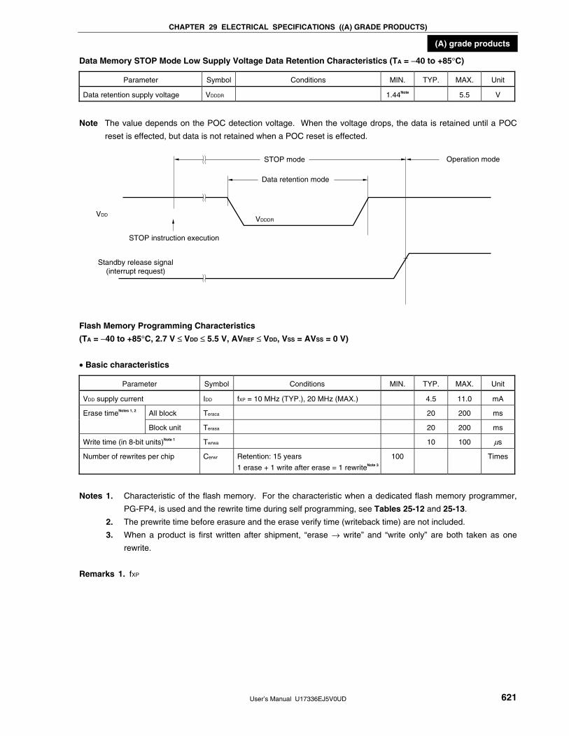

User’s Manual U17336EJ5V0UD 622
CHAPTER 30 ELECTRICAL SPECIFICATIONS ((A2) GRADE PRODUCTS: TA = −40 to +110°C)
Target products: μPD78F0511(A2), 78F0512(A2), 78F0513(A2), 78F0514(A2), 78F0515(A2)
Absolute Maximum Ratings (TA = 25°C) (1/2)
Parameter Symbol Conditions Ratings Unit
VDD −0.5 to +6.5 V
VSS −0.5 to +0.3 V
AVREF −0.5 to VDD + 0.3Note 1 V

CHAPTER 30 ELECTRICAL SPECIFICATIONS ((A2) GRADE PRODUCTS: TA = −40 to +110°C)
User’s Manual U17336EJ5V0UD 623
(A2) grade products: TA = −40 to +110°C
Absolute Maximum Ratings (TA = 25°C) (2/2)
Parameter Symbol Conditions Ratings Unit
Per pin P00, P01, P10 to P17, P30 to P33,
P40Note 1, P41Note 1, P60 to P63, P70,
P71, P72Note 1, P73Note 1, P74Note 2,
P75Note 2, P120, P130Note 2, P140Note 2
30 mA
P00, P01, P40Note 1, P41Note 1, P120,
P130Note 2, P140Note 2
60 mA Total of all pins
200 mA
P10 to P17, P30 to P33, P60 to
P63, P70, P71, P72Note 1, P73Note 1,
P74Note 2, P75Note 2
140 mA
Per pin 1 mA
Total of all pins
P20 to P25, P26Note 1, P27Note 1
5 mA
Per pin 4 mA
Output current, low IOL
Total of all pins
P121 to P124
10 mA
Operating ambient
temperature
TA −40 to +110 °C
Storage temperature Tstg −65 to +150 °C
Notes 1. 44-pin and 48-pin products only.
2. 48-pin products only.
Caution Product quality may suffer if the absolute maximum rating is exceeded even momentarily for any
parameter. That is, the absolute maximum ratings are rated values at which the product is on the
verge of suffering physical damage, and therefore the product must be used under conditions that
ensure that the absolute maximum ratings are not exceeded.
Remark Unless specified otherwise, the characteristics of alternate-function pins are the same as those of port pins.

CHAPTER 30 ELECTRICAL SPECIFICATIONS ((A2) GRADE PRODUCTS: TA = −40 to +110°C)
User’s Manual U17336EJ5V0UD 624
(A2) grade products: TA = −40 to +110°C
X1 Oscillator Characteristics
(TA = −40 to +110°C, 2.7 V ≤ VDD ≤ 5.5 V, VSS = AVSS = 0 V)
Resonator Recommended Circuit Parameter Conditions MIN. TYP. MAX. Unit
4.0 V ≤ VDD ≤ 5.5 V 1.0Note 2 20.0 Ceramic
resonator
C1
X2X1VSS
C2
X1 clock
oscillation
frequency (fX)Note 1 2.7 V ≤ VDD < 4.0 V 1.0Note 2 10.0
MHz
4.0 V ≤ VDD ≤ 5.5 V 1.0Note 2 20.0 Crystal
resonator
C1
X2X1VSS
C2
X1 clock
oscillation
frequency (fX)Note 1 2.7 V ≤ VDD < 4.0 V 1.0Note 2 10.0
MHz
Notes 1. Indicates only oscillator characteristics. Refer to AC Characteristics for instruction execution time.
2. 2.0 MHz (MIN.) when using UART6 during on-board programming.
Cautions 1. When using the X1 oscillator, wire as follows in the area enclosed by the broken lines in the
above figures to avoid an adverse effect from wiring capacitance.
• Keep the wiring length as short as possible.
• Do not cross the wiring with the other signal lines.
• Do not route the wiring near a signal line through which a high fluctuating current flows.
• Always make the ground point of the oscillator capacitor the same potential as VSS.
• Do not ground the capacitor to a ground pattern through which a high current flows.
• Do not fetch signals from the oscillator.
2. Since the CPU is started by the internal high-speed oscillation clock after a reset release, check
the X1 clock oscillation stabilization time using the oscillation stabilization time counter status
register (OSTC) by the user. Determine the oscillation stabilization time of the OSTC register
and oscillation stabilization time select register (OSTS) after sufficiently evaluating the
oscillation stabilization time with the resonator to be used.
Remark For the resonator selection and oscillator constant, customers are requested to either evaluate the
oscillation themselves or apply to the resonator manufacturer for evaluation.

CHAPTER 30 ELECTRICAL SPECIFICATIONS ((A2) GRADE PRODUCTS: TA = −40 to +110°C)
User’s Manual U17336EJ5V0UD 625
(A2) grade products: TA = −40 to +110°C
Internal Oscillator Characteristics
(TA = −40 to +110°C, 2.7 V ≤ VDD ≤ 5.5 V, VSS = AVSS = 0 V)
Resonator Parameter Conditions MIN. TYP. MAX. Unit
RSTS = 1 7.6 8.0 8.4 MHz 8 MHz internal oscillator Internal high-speed oscillation
clock frequency (fRH)Note RSTS = 0 2.48 5.6 9.86 MHz
240 kHz internal oscillator Internal low-speed oscillation
clock frequency (fRL)
216 240 264 kHz
Note Indicates only oscillator characteristics. Refer to AC Characteristics for instruction execution time.
Remark RSTS: Bit 7 of the internal oscillation mode register (RCM)
XT1 Oscillator Characteristics
(TA = −40 to +110°C, 2.7 V ≤ VDD ≤ 5.5 V, VSS = AVSS = 0 V)
Resonator Recommended Circuit Parameter Conditions MIN. TYP. MAX. Unit
Crystal
resonator
XT1VSS XT2
C4 C3
Rd
XT1 clock oscillation
frequency (fXT)Note
32 32.768 35 kHz
Note Indicates only oscillator characteristics. Refer to AC Characteristics for instruction execution time.
Cautions 1. When using the XT1 oscillator, wire as follows in the area enclosed by the broken lines in the
above figure to avoid an adverse effect from wiring capacitance.
• Keep the wiring length as short as possible.
• Do not cross the wiring with the other signal lines.
• Do not route the wiring near a signal line through which a high fluctuating current flows.
• Always make the ground point of the oscillator capacitor the same potential as VSS.
• Do not ground the capacitor to a ground pattern through which a high current flows.
• Do not fetch signals from the oscillator.
2. The XT1 oscillator is designed as a low-amplitude circuit for reducing power consumption, and
is more prone to malfunction due to noise than the X1 oscillator. Particular care is therefore
required with the wiring method when the XT1 clock is used.
Remark For the resonator selection and oscillator constant, customers are requested to either evaluate the
oscillation themselves or apply to the resonator manufacturer for evaluation.

CHAPTER 30 ELECTRICAL SPECIFICATIONS ((A2) GRADE PRODUCTS: TA = −40 to +110°C)
User’s Manual U17336EJ5V0UD 626
(A2) grade products: TA = −40 to +110°C
DC Characteristics (1/5)
(TA = −40 to +110°C, 2.7 V ≤ VDD ≤ 5.5 V, AVREF ≤ VDD, VSS = AVSS = 0 V)
Parameter Symbol Conditions MIN. TYP. MAX. Unit
4.0 V ≤ VDD ≤ 5.5 V −2.5 mA Per pin for P00, P01, P10 to P17,
P30 to P33, P40Note 2, P41Note 2, P70, P71,
P72Note 2, P73Note 2, P74Note 3, P75Note 3, P120,
P130Note 3, P140Note 3
2.7 V ≤ VDD < 4.0 V −2.0 mA
4.0 V ≤ VDD ≤ 5.5 V −7.5 mA Total of pinsNote 5 P00, P01, P40Note 2,
P41Note 2, P120, P130Note 3, P140Note 3 2.7 V ≤ VDD < 4.0 V −6.0 mA
4.0 V ≤ VDD ≤ 5.5 V −12.5 mA Total of pinsNote 5 P10 to P17, P30 to P33,
P70, P71, P72Note 2, P73Note 2, P74Note 3,
P75Note 3 2.7 V ≤ VDD < 4.0 V −10.0 mA
4.0 V ≤ VDD ≤ 5.5 V −16.0 mA
IOH1
Total of all pinsNote 5
2.7 V ≤ VDD < 4.0 V −14.0 mA
Per pin for P20 to P25, P26Note 2, P27Note 2 AVREF = VDD −0.1 mA
Output current,
highNote 1
IOH2
Per pin for P121 to P124 −0.1 mA
4.0 V ≤ VDD ≤ 5.5 V 5.0 mA Per pin for P00, P01, P10 to P17,
P30 to P33, P40Note 2, P41Note 2, P70, P71,
P72Note 2, P73Note 2, P74Note 3, P75Note 3, P120,
P130Note 3, P140Note 3
2.7 V ≤ VDD < 4.0 V 3.0 mA
4.0 V ≤ VDD ≤ 5.5 V 10.0 mA Per pin for P60 to P63
2.7 V ≤ VDD < 4.0 V 3.0 mA
4.0 V ≤ VDD ≤ 5.5 V 13.0 mA Total of pinsNote 5 P00, P01, P40Note 2,
P41Note 2, P120, P130Note 3, P140Note 3 2.7 V ≤ VDD < 4.0 V 10.0 mA
4.0 V ≤ VDD ≤ 5.5 V 25.0 mA Total of pinsNote 5 P10 to P17, P30 to P33,
P60 to P63, P70, P71, P72Note 2, P73Note 2,
P74Note 3, P75Note 3 2.7 V ≤ VDD < 4.0 V 20.0 mA
4.0 V ≤ VDD ≤ 5.5 V 38.0 mA
Output current,
lowNote 3
IOL1
Total of all pinsNote 4
2.7 V ≤ VDD < 4.0 V 30.0 mA
Notes 1. Value of current at which the device operation is guaranteed even if the current flows from VDD to an output
pin.
2. 44-pin and 48-pin products only.
3. 48-pin products only.
4. Value of current at which the device operation is guaranteed even if the current flows from an output pin to
GND.
5. Specification under conditions where the duty factor is 70% (time for which current is output is 0.7 × t and
time for which current is not output is 0.3 × t, where t is a specific time). The total output current of the pins
at a duty factor of other than 70% can be calculated by the following expression.
• Where the duty factor of IOH is n%: Total output current of pins = (IOH × 0.7)/(n × 0.01)
<Example> Where the duty factor is 50%, IOH = 20.0 mA
Total output current of pins = (20.0 × 0.7)/(50 × 0.01) = 28.0 mA
However, the current that is allowed to flow into one pin does not vary depending on the duty factor. A
current higher than the absolute maximum rating must not flow into one pin.
Remark Unless specified otherwise, the characteristics of alternate-function pins are the same as those of port pins.

CHAPTER 30 ELECTRICAL SPECIFICATIONS ((A2) GRADE PRODUCTS: TA = −40 to +110°C)
User’s Manual U17336EJ5V0UD 627
(A2) grade products: TA = −40 to +110°C
DC Characteristics (2/5)
(TA = −40 to +110°C, 2.7 V ≤ VDD ≤ 5.5 V, AVREF ≤ VDD, VSS = AVSS = 0 V)
Parameter Symbol Conditions MIN. TYP. MAX. Unit
Per pin for P20 to P25, P26Note 2,
P27Note 2
AVREF = VDD 0.4 mA Output current, lowNote 1 IOL2
Per pin for P121 to P124 0.4 mA
VIH1 P12, P13, P15, P40Note 2, P41Note 2, P121 to P124 0.7VDD VDD V
VIH2 P00, P01, P10, P11, P14, P16, P17, P30 to P33, P70,
P71, P72Note 2, P73Note 2, P74Note 3, P75Note 3, P120,
P140Note 3, RESET, EXCLK, EXCLKS
0.8VDD VDD V
VIH3 P20 to P25, P26Note 2, P27Note 2 AVREF = VDD 0.7AVREF AVREF V
Input voltage, high
VIH4 P60 to P63 0.7VDD 6.0 V
VIL1 P12, P13, P15, P40, P41, P60 to P63, P121 to P124 0 0.3VDD V
VIL2 P00, P01, P10, P11, P14, P16, P17, P30 to P33,
P70 to P73, P74Note 2, P75Note 2, P120, P140Note 2, RESET,
EXCLK, EXCLKS
0 0.2VDD V
Input voltage, low
VIL3 P20 to P25, P26Note 2, P27Note 2 AVREF = VDD 0 0.3AVREF V
4.0 V ≤ VDD ≤ 5.5 V,
IOH1 = −2.5 mA
VDD − 0.7 V VOH1 P00, P01, P10 to P17,
P30 to P33, P40Note 2, P41Note 2,
P70, P71, P72Note 2, P73Note 2,
P74Note 3, P75Note 3, P120, P130Note 3,
P140Note 3
2.7 V ≤ VDD < 4.0 V,
IOH1 = −2.0 mA
VDD − 0.5 V
P20 to P25, P26Note 2, P27Note 2 AVREF = VDD,
IOH2 = −100 μA
VDD − 0.5 V
Output voltage, high
VOH2
P121 to P124 IOH2 = −100 μA VDD − 0.5 V
Notes 1. Value of current at which the device operation is guaranteed even if the current flows from an output pin to
GND.
2. 44-pin and 48-pin products only.
3. 48-pin products only.
Remark Unless specified otherwise, the characteristics of alternate-function pins are the same as those of port pins.

CHAPTER 30 ELECTRICAL SPECIFICATIONS ((A2) GRADE PRODUCTS: TA = −40 to +110°C)
User’s Manual U17336EJ5V0UD 628
(A2) grade products: TA = −40 to +110°C
DC Characteristics (3/5)
(TA = −40 to +110°C, 2.7 V ≤ VDD ≤ 5.5 V, AVREF ≤ VDD, VSS = AVSS = 0 V)
Parameter Symbol Conditions MIN. TYP. MAX. Unit
4.0 V ≤ VDD ≤ 5.5 V, IOL1 = 5.0 mA
0.7 V VOL1 P00, P01, P10 to P17, P30 to P33, P40Note 1, P41Note 1, P70, P71, P72Note 1, P73Note 1, P74Note 2, P75Note 2, P120, P130Note 2, P140Note 2
2.7 V ≤ VDD < 4.0 V, IOL1 = 3.0 mA
0.7 V
P20 to P25, P26Note 1, P27Note 1 AVREF = VDD, IOL2 = 0.4 mA
0.4 V VOL2
P121 to P124 IOL2 = 0.4 mA 0.4 V
4.0 V ≤ VDD ≤ 5.5 V, IOL3 = 10.0 mA
2.0 V
4.0 V ≤ VDD ≤ 5.5 V, IOL3 = 3.0 mA
0.4 V
Output voltage, low
VOL3 P60 to P63
2.7 V ≤ VDD < 4.0 V, IOL3 = 3.0 mA
0.6 V
ILIH1 P00, P01, P10 to P17, P30 to P33,
P40Note 1, P41Note 1, P60 to P63, P70,
P71, P72Note 1, P73Note 1, P74Note 2,
P75Note 2, P120, P140Note 2, FLMD0,
RESET
VI = VDD 3 μA
ILIH2 P20 to P25, P26Note 1, P27Note 1 VI = AVREF = VDD 3 μA
I/O port mode 3 μA
Input leakage
current, high
ILIH3 P121 to P124
(X1, X2, XT1, XT2)
VI = VDD
OSC mode 20 μA
ILIL1 P00, P01, P10 to P17, P30 to P33,
P40Note 1, P41Note 1, P60 to P63, P70,
P71, P72Note 1, P73Note 1, P74Note 2,
P75Note 2, P120, P140Note 2, FLMD0,
RESET
VI = VSS −3 μA
ILIL2 P20 to P25, P26Note 1, P27Note 1 VI = VSS, AVREF = VDD −3 μA
I/O port mode −3 μA
Input leakage
current, low
ILIL3 P121 to P124
(X1, X2, XT1, XT2)
VI = VSS
OSC mode −20 μA
Pull-up resistance RU VI = VSS 10 20 100 kΩ
VIL In normal operation mode 0 0.2VDD V FLMD0 supply
voltage VIH In self programming mode 0.8VDD VDD V
Notes 1. 44-pin and 48-pin products only.
2. 48-pin products only.
Remark Unless specified otherwise, the characteristics of alternate-function pins are the same as those of port pins.

CHAPTER 30 ELECTRICAL SPECIFICATIONS ((A2) GRADE PRODUCTS: TA = −40 to +110°C)
User’s Manual U17336EJ5V0UD 629
(A2) grade products: TA = −40 to +110°C
DC Characteristics (4/5)
(TA = −40 to +110°C, 2.7 V ≤ VDD ≤ 5.5 V, AVREF ≤ VDD, VSS = AVSS = 0 V)
Parameter Symbol Conditions MIN. TYP. MAX. Unit
Square wave input 3.2 7.2 fXH = 20 MHzNote 2,
VDD = 5.0 V Resonator connection 4.5 9.0
mA
Square wave input 1.6 3.7 fXH = 10 MHzNotes 2, 3,
VDD = 5.0 V Resonator connection 2.3 5.1
mA
Square wave input 1.5 3.6 fXH = 10 MHzNotes 2, 3,
VDD = 3.0 V Resonator connection 2.2 4.2
mA
Square wave input 0.9 2.1 fXH = 5 MHzNotes 2, 3,
VDD = 3.0 V Resonator connection 1.3 2.6
mA
fRH = 8 MHzNote 4, VDD = 5.0 V 1.4 3.3 mA
Square wave input 6 93
IDD1 Operating
mode
fSUB = 32.768 kHzNote 5,
VDD = 5.0 V Resonator connection 15 100
μA
Square wave input 0.8 3.4 fXH = 20 MHzNote 2,
VDD = 5.0 V Resonator connection 2.0 5.8
mA
Square wave input 0.4 1.7 fXH = 10 MHzNotes 2, 3,
VDD = 5.0 V Resonator connection 1.0 3.2
mA
Square wave input 0.2 0.85 fXH = 5 MHzNotes 2, 3,
VDD = 3.0 V Resonator connection 0.5 1.5
mA
fRH = 8 MHzNote 4, VDD = 5.0 V 0.4 1.6 mA
Square wave input 3.0 89
IDD2 HALT mode
fSUB = 32.768 kHzNote 5,
VDD = 5.0 V Resonator connection 12 93
μA
VDD = 5.0 V 1 60 μA
Supply currentNote 1
IDD3 STOP modeNote 6
VDD = 5.0 V, TA = −40 to +70°C 1 10 μA
Notes 1. Total current flowing into the internal power supply (VDD), including the peripheral operation current and
the input leakage current flowing when the level of the input pin is fixed to VDD or VSS. However, the
current flowing into the pull-up resistors and the output current of the port are not included.
2. Not including the operating current of the 8 MHz internal oscillator, 240 kHz internal oscillator, and XT1
oscillator, and the current flowing into the A/D converter, watchdog timer and LVI circuit.
3. When AMPH (bit 0 of clock operation mode select register (OSCCTL)) = 0.
4. Not including the operating current of the X1 oscillator, XT1 oscillator, and 240 kHz internal oscillator, and
the current flowing into the A/D converter, watchdog timer and LVI circuit.
5. Not including the operating current of the X1 oscillator, 8 MHz internal oscillator, and 240 kHz internal
oscillator, and the current flowing into the A/D converter, watchdog timer and LVI circuit.
6. Not including the operating current of the 240 kHz internal oscillator and XT1 oscillator, and the current
flowing into the A/D converter, watchdog timer and LVI circuit.
Remarks 1. fXH: High-speed system clock frequency (X1 clock oscillation frequency or external main system clock
frequency)
2. fRH: Internal high-speed oscillation clock frequency
3. fSUB: Subsystem clock frequency (XT1 clock oscillation frequency or external subsystem clock
frequency)

CHAPTER 30 ELECTRICAL SPECIFICATIONS ((A2) GRADE PRODUCTS: TA = −40 to +110°C)
User’s Manual U17336EJ5V0UD 630
(A2) grade products: TA = −40 to +110°C
DC Characteristics (5/5)
(TA = −40 to +110°C, 2.7 V ≤ VDD ≤ 5.5 V, AVREF ≤ VDD, VSS = AVSS = 0 V)
Parameter Symbol Conditions MIN. TYP. MAX. Unit
A/D converter
operating current
IADCNote 1 2.7 V ≤ AVREF ≤ VDD, ADCE = 1 0.86 2.5 mA
Watchdog timer
operating current
IWDTNote 2 During 240 kHz internal low-speed oscillation clock
operation
5 13 μA
LVI operating current ILVINote 3 9 24 μA
Notes 1. Current flowing only to the A/D converter (AVREF). The current value of the 78K0/KC2 is the sum of IDD1 or
IDD2 and IADC when the A/D converter operates in an operation mode or the HALT mode.
2. Current flowing only to the watchdog timer, including the operating current of the 240 kHz internal
oscillator. The current value of the 78K0/KC2 is the sum of IDD2 or IDD3 and IWDT when the watchdog timer
operates in the HALT or STOP mode.
3. Current flowing only to the LVI circuit. The current value of the 78K0/KC2 is the sum of IDD2 or IDD3 and ILVI
when the LVI circuit operates in the HALT or STOP mode.

CHAPTER 30 ELECTRICAL SPECIFICATIONS ((A2) GRADE PRODUCTS: TA = −40 to +110°C)
User’s Manual U17336EJ5V0UD 631
(A2) grade products: TA = −40 to +110°C
AC Characteristics
(1) Basic operation
(TA = −40 to +110°C, 2.7 V ≤ VDD ≤ 5.5 V, AVREF ≤ VDD, VSS = AVSS = 0 V)
Parameter Symbol Conditions MIN. TYP. MAX. Unit
4.0 V ≤ VDD ≤ 5.5 V 0.1 32 μs Main system
clock (fXP)
operation 2.7 V ≤ VDD < 4.0 V 0.2 32 μs
Instruction cycle (minimum
instruction execution time)
TCY
Subsystem clock (fSUB) operation 114 122 125 μs
4.0 V ≤ VDD ≤ 5.5 V 20 MHz fPRS = fXH
(XSEL = 1) 2.7 V ≤ VDD < 4.0 V 10 MHz
Peripheral hardware clock
frequency
fPRS
fPRS = fRH
(XSEL = 0)
2.7 V ≤ VDD < 5.5 V 7.6 8.4 MHz
4.0 V ≤ VDD ≤ 5.5 V 1.0Note 1 20.0 MHz External main system clock
frequency
fEXCLK
2.7 V ≤ VDD < 4.0 V 1.0Note 1 10.0 MHz
4.0 V ≤ VDD ≤ 5.5 V 24 ns External main system clock input
high-level width, low-level width
tEXCLKH,
tEXCLKL 2.7 V ≤ VDD < 4.0 V 48 ns
External subsystem clock
frequency
fEXCLKS 32 32.768 35 kHz
External subsystem clock input
high-level width, low-level width
tEXCLKSH,
tEXCLKSL
12 μs
4.0 V ≤ VDD ≤ 5.5 V 2/fsam + 0.1Note 2 μs TI000, TI010 input high-level
width, low-level width
tTIH0,
tTIL0 2.7 V ≤ VDD < 4.0 V 2/fsam + 0.2Note 2 μs
TI50, TI51 input frequency fTI5 10 MHz
TI50, TI51 input high-level width,
low-level width
tTIH5,
tTIL5
50 ns
Interrupt input high-level width,
low-level width
tINTH,
tINTL
1 μs
Key interrupt input low-level width tKR 250 ns
RESET low-level width tRSL 10 μs
Notes 1. 2.0 MHz (MIN.) when using UART6 during on-board programming.
2. Selection of fsam = fPRS, fPRS/4, fPRS/256 is possible using bits 0 and 1 (PRM000, PRM001) of prescaler
mode register 00 (PRM00). Note that when selecting the TI000 valid edge as the count clock, fsam =
fPRS.

CHAPTER 30 ELECTRICAL SPECIFICATIONS ((A2) GRADE PRODUCTS: TA = −40 to +110°C)
User’s Manual U17336EJ5V0UD 632
(A2) grade products: TA = −40 to +110°C
TCY vs. VDD (Main System Clock Operation)
5.0
1.0
2.0
0.4
0.2
0.1
0
10
1.0 2.0 3.0 4.0 5.0 6.05.5
2.7
100
0.01
32
Supply voltage VDD [V]
Cyc
le ti
me
TC
Y [
s]
Guaranteed operation range
μ
AC Timing Test Points
VIH
VIL
Test pointsVIH
VIL
External Main System Clock Timing, External Subsystem Clock Timing
EXCLK0.8VDD (MIN.)
0.2VDD (MAX.)
1/fEXCLK
tEXCLKL tEXCLKH
1/fEXCLKS
tEXCLKSL tEXCLKSH
EXCLKS0.8VDD (MIN.)
0.2VDD (MAX.)

CHAPTER 30 ELECTRICAL SPECIFICATIONS ((A2) GRADE PRODUCTS: TA = −40 to +110°C)
User’s Manual U17336EJ5V0UD 633
(A2) grade products: TA = −40 to +110°C
TI Timing
TI000, TI010
tTIL0 tTIH0
TI50, TI51
1/fTI5
tTIL5 tTIH5
Interrupt Request Input Timing
INTP0 to INTP5, INTP6Note
tINTL tINTH
Note 48-pin products only.
Key Interrupt Input Timing
KR0, KR1, KR2Note, KR3Note
tKR
Note 44-pin and 48-pin products only
RESET Input Timing
RESET
tRSL

CHAPTER 30 ELECTRICAL SPECIFICATIONS ((A2) GRADE PRODUCTS: TA = −40 to +110°C)
User’s Manual U17336EJ5V0UD 634
(A2) grade products: TA = −40 to +110°C
(2) Serial interface
(TA = −40 to +110°C, 2.7 V ≤ VDD ≤ 5.5 V, AVREF ≤ VDD, VSS = AVSS = 0 V)
(a) UART6 (dedicated baud rate generator output)
Parameter Symbol Conditions MIN. TYP. MAX. Unit
Transfer rate 625 kbps
(b) UART0 (dedicated baud rate generator output)
Parameter Symbol Conditions MIN. TYP. MAX. Unit
Transfer rate 625 kbps
(c) IIC0
Standard Mode High-Speed Mode Parameter Symbol Conditions
MIN. MAX. MIN. MAX.
Unit
SCL0 clock frequency fSCL 0 100 0 400 kHz
Setup time of restart condition tSU:STA 4.7 − 0.6 − μs
Hold timeNote 1 tHD:STA 4.0 − 0.6 − μs
Internal clock operation 4.7 − 1.3 − μs Hold time when SCL0 = “L” tLOW
EXSCL0 clock (6.4 MHz) operation 4.7 − 1.25 − μs
Hold time when SCL0 = “H” tHIGH 4.0 − 0.6 − μs
Data setup time (reception) tSU:DAT 250 − 100 − ns
0.9Note 4 DFC0 = 0 0 3.45 0
1.00Note 5
μs
0.9Note 6
fW = fXH/2N or
fW = fEXSCL0 selectedNote 3
DFC0 = 1 − − 0
1.125Note 7
μs
DFC0 = 0 0 3.45 0 1.05 μs
Data setup time
(transmission)Note 2
tHD:DAT
fW = fRH/2N selectedNote 3
DFC0 = 1 − − 0 1.184 μs
Setup time of stop condition tSU:STO 4.0 − 0.6 − μs
Bus free time tBUF 4.7 − 1.3 − μs
Notes 1. The first clock pulse is generated after this period when the start/restart condition is detected.
2. The maximum value (MAX.) of tHD:DAT is during normal transfer and a wait state is inserted in the ACK
(acknowledge) timing.
3. fW indicates the IIC0 transfer clock selected by the IICCL and IICX0 registers.
4. When fW ≥ 4.4 MHz is selected
5. When fW < 4.4 MHz is selected
6. When fW ≥ 5 MHz is selected
7. When fW < 5 MHz is selected

CHAPTER 30 ELECTRICAL SPECIFICATIONS ((A2) GRADE PRODUCTS: TA = −40 to +110°C)
User’s Manual U17336EJ5V0UD 635
(A2) grade products: TA = −40 to +110°C
(d) CSI10 (master mode, SCK10... internal clock output)
Parameter Symbol Conditions MIN. TYP. MAX. Unit
4.0 V ≤ VDD ≤ 5.5 V 200 ns SCK10 cycle time tKCY1
2.7 V ≤ VDD < 4.0 V 400 ns
4.0 V ≤ VDD ≤ 5.5 V tKCY1/2 − 20Note 1 ns SCK10 high-/low-level width tKH1,
tKL1 2.7 V ≤ VDD < 4.0 V tKCY1/2 − 30Note 1 ns
4.0 V ≤ VDD ≤ 5.5 V 70 ns SI10 setup time (to SCK10↑) tSIK1
2.7 V ≤ VDD < 4.0 V 100 ns
SI10 hold time (from SCK10↑) tKSI1 30 ns
Delay time from SCK10↓ to
SO10 output
tKSO1 C = 50 pFNote 2 40 ns
Notes 1. This value is when high-speed system clock (fXH) is used.
2. C is the load capacitance of the SCK10 and SO10 output lines.
(e) CSI10 (slave mode, SCK10... external clock input)
Parameter Symbol Conditions MIN. TYP. MAX. Unit
SCK10 cycle time tKCY2 400 ns
SCK10 high-/low-level width tKH2,
tKL2
tKCY2/2 ns
SI10 setup time (to SCK10↑) tSIK2 80 ns
SI10 hold time (from SCK10↑) tKSI2 50 ns
Delay time from SCK10↓ to
SO10 output
tKSO2 C = 50 pFNote 120 ns
Note C is the load capacitance of the SO10 output line.

CHAPTER 30 ELECTRICAL SPECIFICATIONS ((A2) GRADE PRODUCTS: TA = −40 to +110°C)
User’s Manual U17336EJ5V0UD 636
(A2) grade products: TA = −40 to +110°CSerial Transfer Timing
IIC0:
tLOW
tHIGH
tHD:STA tSU:DAT
tSU:STA tHD:STAtHD:DAT
SCL0
SDA0
tBUF
tSU:STO
Stop condition
Start condition
Restart condition
Stop condition
CSI10:
SI10
SO10
tKCYm
tKLm tKHm
tSIKm tKSIm
Input data
tKSOm
Output data
SCK10
Remark m = 1, 2


CHAPTER 30 ELECTRICAL SPECIFICATIONS ((A2) GRADE PRODUCTS: TA = −40 to +110°C)
User’s Manual U17336EJ5V0UD 638
(A2) grade products: TA = −40 to +110°C
Supply Voltage Rise Time (TA = −40 to +110°C, VSS = 0 V)
Parameter Symbol Conditions MIN. TYP. MAX. Unit
Maximum time to rise to 2.7 V (VDD (MIN.))
(VDD: 0 V → 2.7 V)
tPUP1 POCMODE (option byte) = 0,
when RESET input is not used
3.6 ms
Maximum time to rise to 2.7 V (VDD (MIN.))
(releasing RESET input → VDD: 2.7 V)
tPUP2 POCMODE (option byte) = 0,
when RESET input is used
1.9 ms
Supply Voltage Rise Time Timing
• When RESET pin input is not used • When RESET pin input is used
Supply voltage
(VDD)
Time
2.7 V
tPUP1
Supply voltage
(VDD)
Time
2.7 V
tPUP2
VPOC
RESET pin
2.7 V POC Circuit Characteristics (TA = −40 to +110°C, VSS = 0 V)
Parameter Symbol Conditions MIN. TYP. MAX. Unit
Detection voltage on application of supply
voltage
VDDPOC POCMODE (option byte) = 1 2.50 2.70 2.90 V

CHAPTER 30 ELECTRICAL SPECIFICATIONS ((A2) GRADE PRODUCTS: TA = −40 to +110°C)
User’s Manual U17336EJ5V0UD 639
(A2) grade products: TA = −40 to +110°C
LVI Circuit Characteristics (TA = −40 to +110°C, VPOC ≤ VDD ≤ 5.5 V, AVREF ≤ VDD, VSS = 0 V)
Parameter Symbol Conditions MIN. TYP. MAX. Unit
VLVI0 4.14 4.24 4.34 V
VLVI1 3.99 4.09 4.19 V
VLVI2 3.83 3.93 4.03 V
VLVI3 3.68 3.78 3.88 V
VLVI4 3.52 3.62 3.72 V
VLVI5 3.37 3.47 3.57 V
VLVI6 3.22 3.32 3.42 V
VLVI7 3.06 3.16 3.26 V
VLVI8 2.91 3.01 3.11 V
Supply voltage level
VLVI9 2.75 2.85 2.95 V
Detection
voltage
External input pinNote 1 EXLVI EXLVI < VDD, 2.7 V ≤ VDD ≤ 5.5 V 1.11 1.21 1.31 V
Minimum pulse width tLW 200 μs
Operation stabilization wait timeNote 2 tLWAIT 10 μs
Notes 1. The EXLVI/P120/INTP0 pin is used.
2. Time required from setting bit 7 (LVION) of the low-voltage detection register (LVIM) to 1 to operation
stabilization
Remark VLVI(n − 1) > VLVIn: n = 1 to 9
LVI Circuit Timing
Supply voltage
(VDD)
Time
Detection voltage (MIN.)
Detection voltage (TYP.)
Detection voltage (MAX.)
tLW
tLWAIT
LVION ← 1

CHAPTER 30 ELECTRICAL SPECIFICATIONS ((A2) GRADE PRODUCTS: TA = −40 to +110°C)
User’s Manual U17336EJ5V0UD 640
(A2) grade products: TA = −40 to +110°C
Data Memory STOP Mode Low Supply Voltage Data Retention Characteristics (TA = −40 to +110°C)
Parameter Symbol Conditions MIN. TYP. MAX. Unit
Data retention supply voltage VDDDR 1.44Note 5.5 V
Note The value depends on the POC detection voltage. When the voltage drops, the data is retained until a POC
reset is effected, but data is not retained when a POC reset is effected.
VDD
STOP instruction execution
Standby release signal(interrupt request)
STOP mode
Data retention mode
VDDDR
Operation mode
Flash Memory Programming Characteristics
(TA = −40 to +110°C, 2.7 V ≤ VDD ≤ 5.5 V, AVREF ≤ VDD, VSS = AVSS = 0 V)
• Basic characteristics
Parameter Symbol Conditions MIN. TYP. MAX. Unit
VDD supply current IDD fXP = 10 MHz (TYP.), 20 MHz (MAX.) 4.5 14.0 mA
All block Teraca 20 200 ms Erase timeNotes 1, 2
Block unit Terasa 20 200 ms
Write time (in 8-bit units)Note 1 Twrwa 10 100 μs
Number of rewrites per chip Cerwr Retention: 15 years
1 erase + 1 write after erase = 1 rewriteNote 3
100 Times
Notes 1. Characteristic of the flash memory. For the characteristic when a dedicated flash memory programmer,
PG-FP4, is used and the rewrite time during self programming, see Tables 25-12 and 25-13.
2. The prewrite time before erasure and the erase verify time (writeback time) are not included.
3. When a product is first written after shipment, “erase → write” and “write only” are both taken as one
rewrite.
Remarks 1. fXP: Main system clock oscillation frequency
2. For serial write operation characteristics, refer to 78K0/Kx2 Flash Memory Programming
(Programmer) Application Note (U17739E).

User’s Manual U17336EJ5V0UD 641
CHAPTER 31 ELECTRICAL SPECIFICATIONS ((A2) GRADE PRODUCTS: TA = −40 to +125°C)
Target products: μPD78F0511(A2), 78F0512(A2), 78F0513(A2), 78F0514(A2), 78F0515(A2)
Absolute Maximum Ratings (TA = 25°C) (1/2)
Parameter Symbol Conditions Ratings Unit
VDD −0.5 to +6.5 V
VSS −0.5 to +0.3 V
AVREF −0.5 to VDD + 0.3Note 1 V
Supply voltage
AVSS −0.5 to +0.3 V
REGC pin input voltage VIREGC −0.5 to +3.6 and ≤ VDD V
VI1 P00, P01, P10 to P17, P20 to P25, P26Note 2, P27Note 2,
P30 to P33, P40Note 2, P41Note 2, P70 , P71, P72Note 2,
P73Note 2, P74Note 3, P75Note 3, P120 to P124, P140Note 3,
X1, X2, XT1, XT2, RESET, FLMD0
−0.3 to VDD + 0.3Note 1 V Input voltage
VI2 P60 to P63 (N-ch open drain) −0.3 to +6.5 V
Output voltage VO −0.3 to VDD + 0.3Note 1 V
Analog input voltage VAN ANI0 to ANI5, ANI6Note 2, ANI7Note 2 −0.3 to AVREF + 0.3Note 1
and −0.3 to VDD + 0.3Note 1
V
Per pin P00, P01, P10 to P17, P30 to P33,
P40Note 2, P41Note 2, P70, P71, P72Note 2,
P73Note 2, P74Note 3, P75Note 3, P120,
P130Note 3, P140Note 3
−10 mA
P00, P01, P40Note 2, P41Note 2, P120,
P130Note 3, P140Note 3
−25 mA Total of all pins
−80 mA
P10 to P17, P30 to P33, P70, P71,
P72Note 2, P73Note 2, P74Note 3, P75Note 3
−55 mA
Per pin −0.5 mA
Total of all pins
P20 to P25, P26Note 2, P27Note 2
−2 mA
Per pin −1 mA
Output current, high IOH
Total of all pins
P121 to P124
−4 mA
Notes 1. Must be 6.5 V or lower.
2. 44-pin and 48-pin products only.
3. 48-pin products only.
Caution Product quality may suffer if the absolute maximum rating is exceeded even momentarily for any
parameter. That is, the absolute maximum ratings are rated values at which the product is on the
verge of suffering physical damage, and therefore the product must be used under conditions that
ensure that the absolute maximum ratings are not exceeded.
Remark Unless specified otherwise, the characteristics of alternate-function pins are the same as those of port pins.
<R>

CHAPTER 31 ELECTRICAL SPECIFICATIONS ((A2) GRADE PRODUCTS: TA = −40 to +125°C)
User’s Manual U17336EJ5V0UD 642
(A2) grade products: TA = −40 to +125°C
Absolute Maximum Ratings (TA = 25°C) (2/2)
Parameter Symbol Conditions Ratings Unit
Per pin P00, P01, P10 to P17, P30 to P33,
P40Note 1, P41Note 1, P60 to P63, P70,
P71, P72Note 1, P73Note 1, P74Note 2,
P75Note 2, P120, P130Note 2, P140Note 2
30 mA
P00, P01, P40Note 1, P41Note 1, P120,
P130Note 2, P140Note 2
60 mA Total of all pins
200 mA
P10 to P17, P30 to P33, P60 to
P63, P70, P71, P72Note 1, P73Note 1,
P74Note 2, P75Note 2
140 mA
Per pin 1 mA
Total of all pins
P20 to P25, P26Note 1, P27Note 1
5 mA
Per pin 4 mA
Output current, low IOL
Total of all pins
P121 to P124
10 mA
Operating ambient
temperature
TA −40 to +125 °C
Storage temperature Tstg −65 to +150 °C
Notes 1. 44-pin and 48-pin products only.
2. 48-pin products only.
Caution Product quality may suffer if the absolute maximum rating is exceeded even momentarily for any
parameter. That is, the absolute maximum ratings are rated values at which the product is on the
verge of suffering physical damage, and therefore the product must be used under conditions that
ensure that the absolute maximum ratings are not exceeded.
Remark Unless specified otherwise, the characteristics of alternate-function pins are the same as those of port pins.
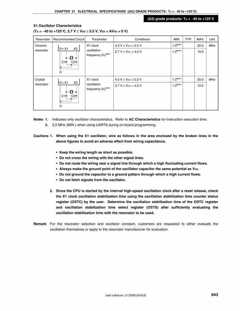
CHAPTER 31 ELECTRICAL SPECIFICATIONS ((A2) GRADE PRODUCTS: TA = −40 to +125°C)
User’s Manual U17336EJ5V0UD 643
(A2) grade products: TA = −40 to +125°C
X1 Oscillator Characteristics
(TA = −40 to +125°C, 2.7 V ≤ VDD ≤ 5.5 V, VSS = AVSS = 0 V)
Resonator Recommended Circuit Parameter Conditions MIN. TYP. MAX. Unit
4.0 V ≤ VDD ≤ 5.5 V 1.0Note 2 20.0 Ceramic
resonator
C1
X2X1VSS
C2
X1 clock
oscillation
frequency (fX)Note 1 2.7 V ≤ VDD < 4.0 V 1.0Note 2 10.0
MHz
4.0 V ≤ VDD ≤ 5.5 V 1.0Note 2 20.0 Crystal
resonator
C1
X2X1VSS
C2
X1 clock
oscillation
frequency (fX)Note 1 2.7 V ≤ VDD < 4.0 V 1.0Note 2 10.0
MHz
Notes 1. Indicates only oscillator characteristics. Refer to AC Characteristics for instruction execution time.
2. 2.0 MHz (MIN.) when using UART6 during on-board programming.
Cautions 1. When using the X1 oscillator, wire as follows in the area enclosed by the broken lines in the
above figures to avoid an adverse effect from wiring capacitance.
• Keep the wiring length as short as possible.
• Do not cross the wiring with the other signal lines.
• Do not route the wiring near a signal line through which a high fluctuating current flows.
• Always make the ground point of the oscillator capacitor the same potential as VSS.
• Do not ground the capacitor to a ground pattern through which a high current flows.
• Do not fetch signals from the oscillator.
2. Since the CPU is started by the internal high-speed oscillation clock after a reset release, check
the X1 clock oscillation stabilization time using the oscillation stabilization time counter status
register (OSTC) by the user. Determine the oscillation stabilization time of the OSTC register
and oscillation stabilization time select register (OSTS) after sufficiently evaluating the
oscillation stabilization time with the resonator to be used.
Remark For the resonator selection and oscillator constant, customers are requested to either evaluate the
oscillation themselves or apply to the resonator manufacturer for evaluation.

CHAPTER 31 ELECTRICAL SPECIFICATIONS ((A2) GRADE PRODUCTS: TA = −40 to +125°C)
User’s Manual U17336EJ5V0UD 644
(A2) grade products: TA = −40 to +125°C
Internal Oscillator Characteristics
(TA = −40 to +125°C, 2.7 V ≤ VDD ≤ 5.5 V, VSS = AVSS = 0 V)
Resonator Parameter Conditions MIN. TYP. MAX. Unit
RSTS = 1 7.6 8.0 8.46 MHz 8 MHz internal oscillator Internal high-speed oscillation
clock frequency (fRH)Note RSTS = 0 2.48 5.6 9.86 MHz
240 kHz internal oscillator Internal low-speed oscillation
clock frequency (fRL)
216 240 264 kHz
Note Indicates only oscillator characteristics. Refer to AC Characteristics for instruction execution time.
Remark RSTS: Bit 7 of the internal oscillation mode register (RCM)
XT1 Oscillator Characteristics
(TA = −40 to +125°C, 2.7 V ≤ VDD ≤ 5.5 V, VSS = AVSS = 0 V)
Resonator Recommended Circuit Parameter Conditions MIN. TYP. MAX. Unit
Crystal
resonator
XT1VSS XT2
C4 C3
Rd
XT1 clock oscillation
frequency (fXT)Note
32 32.768 35 kHz
Note Indicates only oscillator characteristics. Refer to AC Characteristics for instruction execution time.
Cautions 1. When using the XT1 oscillator, wire as follows in the area enclosed by the broken lines in the
above figure to avoid an adverse effect from wiring capacitance.
• Keep the wiring length as short as possible.
• Do not cross the wiring with the other signal lines.
• Do not route the wiring near a signal line through which a high fluctuating current flows.
• Always make the ground point of the oscillator capacitor the same potential as VSS.
• Do not ground the capacitor to a ground pattern through which a high current flows.
• Do not fetch signals from the oscillator.
2. The XT1 oscillator is designed as a low-amplitude circuit for reducing power consumption, and
is more prone to malfunction due to noise than the X1 oscillator. Particular care is therefore
required with the wiring method when the XT1 clock is used.
Remark For the resonator selection and oscillator constant, customers are requested to either evaluate the
oscillation themselves or apply to the resonator manufacturer for evaluation.

CHAPTER 31 ELECTRICAL SPECIFICATIONS ((A2) GRADE PRODUCTS: TA = −40 to +125°C)
User’s Manual U17336EJ5V0UD 645
(A2) grade products: TA = −40 to +125°C
DC Characteristics (1/5)
(TA = −40 to +125°C, 2.7 V ≤ VDD ≤ 5.5 V, AVREF ≤ VDD, VSS = AVSS = 0 V)
Parameter Symbol Conditions MIN. TYP. MAX. Unit
4.0 V ≤ VDD ≤ 5.5 V −1.5 mA Per pin for P00, P01, P10 to P17,
P30 to P33, P40Note 2, P41Note 2, P70, P71,
P72Note 2, P73Note 2, P74Note 3, P75Note 3, P120,
P130Note 3, P140Note 3
2.7 V ≤ VDD < 4.0 V −1.0 mA
4.0 V ≤ VDD ≤ 5.5 V −6.0 mA Total of pinsNote 5 P00, P01, P40Note 2,
P41Note 2, P120, P130Note 3, P140Note 3 2.7 V ≤ VDD < 4.0 V −4.0 mA
4.0 V ≤ VDD ≤ 5.5 V −10.0 mA Total of pinsNote 5 P10 to P17, P30 to P33,
P70, P71, P72Note 2, P73Note 2, P74Note 3,
P75Note 3 2.7 V ≤ VDD < 4.0 V −8.0 mA
4.0 V ≤ VDD ≤ 5.5 V −14.0 mA
IOH1
Total of all pinsNote 5
2.7 V ≤ VDD < 4.0 V −12.0 mA
Per pin for P20 to P25, P26Note 2, P27Note 2 AVREF = VDD −0.1 mA
Output current,
highNote 1
IOH2
Per pin for P121 to P124 −0.1 mA
4.0 V ≤ VDD ≤ 5.5 V 4.0 mA Per pin for P00, P01, P10 to P17,
P30 to P33, P40Note 2, P41Note 2, P70, P71,
P72Note 2, P73Note 2, P74Note 3, P75Note 3, P120,
P130Note 3, P140Note 3
2.7 V ≤ VDD < 4.0 V 2.0 mA
4.0 V ≤ VDD ≤ 5.5 V 8.0 mA Per pin for P60 to P63
2.7 V ≤ VDD < 4.0 V 2.0 mA
4.0 V ≤ VDD ≤ 5.5 V 10.0 mA Total of pinsNote 5 P00, P01, P40Note 2,
P41Note 2, P120, P130Note 3, P140Note 3 2.7 V ≤ VDD < 4.0 V 8.0 mA
4.0 V ≤ VDD ≤ 5.5 V 20.0 mA Total of pinsNote 5 P10 to P17, P30 to P33,
P60 to P63, P70, P71, P72Note 2, P73Note 2,
P74Note 3, P75Note 3 2.7 V ≤ VDD < 4.0 V 16.0 mA
4.0 V ≤ VDD ≤ 5.5 V 30.0 mA
Output current,
lowNote 3
IOL1
Total of all pinsNote 4
2.7 V ≤ VDD < 4.0 V 24.0 mA
Notes 1. Value of current at which the device operation is guaranteed even if the current flows from VDD to an output
pin.
2. 44-pin and 48-pin products only.
3. 48-pin products only.
4. Value of current at which the device operation is guaranteed even if the current flows from an output pin to
GND.
5. Specification under conditions where the duty factor is 70% (time for which current is output is 0.7 × t and
time for which current is not output is 0.3 × t, where t is a specific time). The total output current of the pins
at a duty factor of other than 70% can be calculated by the following expression.
• Where the duty factor of IOH is n%: Total output current of pins = (IOH × 0.7)/(n × 0.01)
<Example> Where the duty factor is 50%, IOH = 20.0 mA
Total output current of pins = (20.0 × 0.7)/(50 × 0.01) = 28.0 mA
However, the current that is allowed to flow into one pin does not vary depending on the duty factor. A
current higher than the absolute maximum rating must not flow into one pin.
Remark Unless specified otherwise, the characteristics of alternate-function pins are the same as those of port pins.
CHAPTER 31 ELECTRICAL SPECIFICATIONS ((A2) GRADE PRODUCTS: TA = −40 to +125°C)
User’s Manual U17336EJ5V0UD 646
(A2) grade products: TA = −40 to +125°C
DC Characteristics (2/5)
(TA = −40 to +125

CHAPTER 31 ELECTRICAL SPECIFICATIONS ((A2) GRADE PRODUCTS: TA = −40 to +125°C)
User’s Manual U17336EJ5V0UD 647
(A2) grade products: TA = −40 to +125°C
DC Characteristics (3/5)
(TA = −40 to +125°C, 2.7 V ≤ VDD ≤ 5.5 V, AVREF ≤ VDD, VSS = AVSS = 0 V)
Parameter Symbol Conditions MIN. TYP. MAX. Unit
4.0 V ≤ VDD ≤ 5.5 V, IOL1 = 4.0 mA
0.7 V VOL1 P00, P01, P10 to P17, P30 to P33, P40Note 1, P41Note 1, P70, P71, P72Note 1, P73Note 1, P74Note 2, P75Note 2, P120, P130Note 2, P140Note 2
2.7 V ≤ VDD < 4.0 V, IOL1 = 2.0 mA
0.7 V
P20 to P25, P26Note 1, P27Note 1 AVREF = VDD, IOL2 = 0.4 mA
0.4 V VOL2
P121 to P124 IOL2 = 0.4 mA 0.4 V
4.0 V ≤ VDD ≤ 5.5 V, IOL3 = 8.0 mA
2.0 V
4.0 V ≤ VDD ≤ 5.5 V, IOL3 = 2.0 mA
0.6 V
Output voltage, low
VOL3 P60 to P63
2.7 V ≤ VDD < 4.0 V, IOL3 = 2.0 mA
0.6 V
ILIH1 P00, P01, P10 to P17, P30 to P33,
P40Note 1, P41Note 1, P60 to P63, P70,
P71, P72Note 1, P73Note 1, P74Note 2,
P75Note 2, P120, P140Note 2, FLMD0,
RESET
VI = VDD 5 μA
ILIH2 P20 to P25, P26Note 1, P27Note 1 VI = AVREF = VDD 5 μA
I/O port mode 5 μA
Input leakage
current, high
ILIH3 P121 to P124
(X1, X2, XT1, XT2)
VI = VDD
OSC mode 20 μA
ILIL1 P00, P01, P10 to P17, P30 to P33,
P40Note 1, P41Note 1, P60 to P63, P70,
P71, P72Note 1, P73Note 1, P74Note 2,
P75Note 2, P120, P140Note 2, FLMD0,
RESET
VI = VSS −5 μA
ILIL2 P20 to P25, P26Note 1, P27Note 1 VI = VSS, AVREF = VDD −5 μA
I/O port mode −5 μA
Input leakage
current, low
ILIL3 P121 to P124
(X1, X2, XT1, XT2)
VI = VSS
OSC mode −20 μA
Pull-up resistance RU VI = VSS 10 20 100 kΩ
VIL In normal operation mode 0 0.2VDD V FLMD0 supply
voltage VIH In self programming mode 0.8VDD VDD V
Notes 1. 44-pin and 48-pin products only.
2. 48-pin products only.
Remark Unless specified otherwise, the characteristics of alternate-function pins are the same as those of port pins.
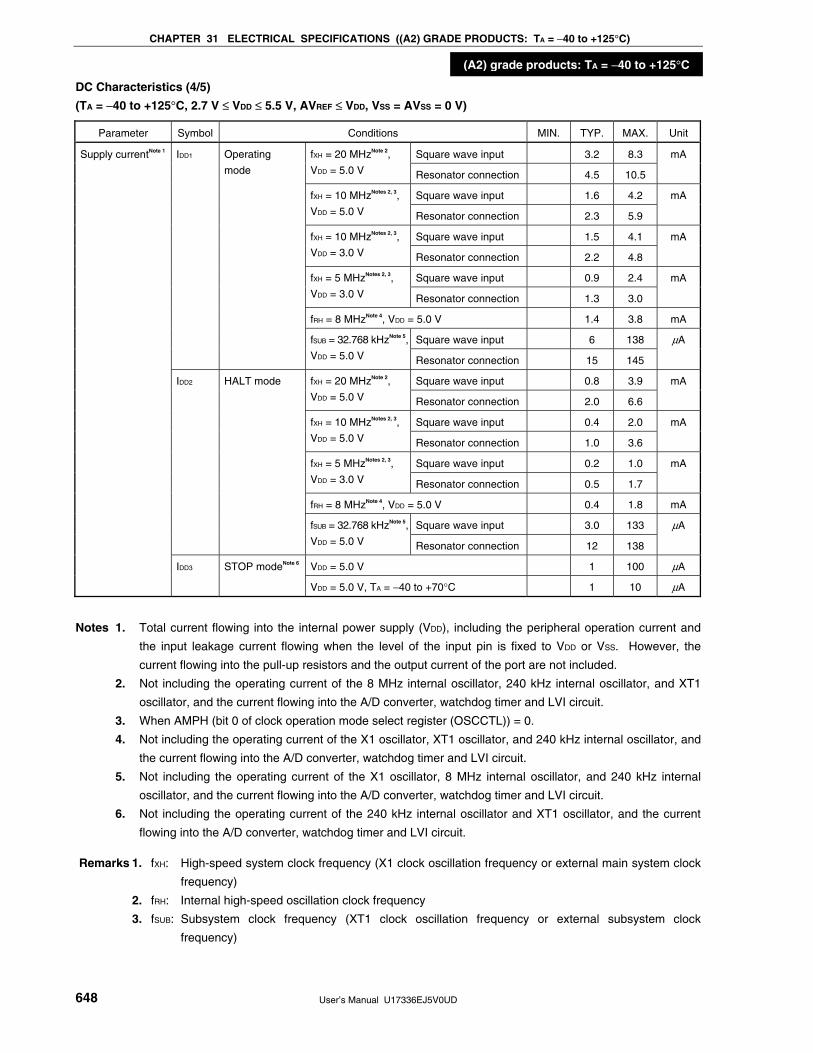
CHAPTER 31 ELECTRICAL SPECIFICATIONS ((A2) GRADE PRODUCTS: TA = −40 to +125°C)
User’s Manual U17336EJ5V0UD 648
(A2) grade products: TA = −40 to +125°C
DC Characteristics (4/5)
(TA = −40 to +125°C, 2.7 V ≤ VDD ≤ 5.5 V, AVREF ≤ VDD, VSS = AVSS = 0 V)
Parameter Symbol Conditions MIN. TYP. MAX. Unit
Square wave input 3.2 8.3 fXH = 20 MHzNote 2,
VDD = 5.0 V Resonator connection 4.5 10.5
mA
Square wave input 1.6 4.2 fXH = 10 MHzNotes 2, 3,
VDD = 5.0 V Resonator connection 2.3 5.9
mA
Square wave input 1.5 4.1 fXH = 10 MHzNotes 2, 3,
VDD = 3.0 V Resonator connection 2.2 4.8
mA
Square wave input 0.9 2.4 fXH = 5 MHzNotes 2, 3,
VDD = 3.0 V Resonator connection 1.3 3.0
mA
fRH = 8 MHzNote 4, VDD = 5.0 V 1.4 3.8 mA
Square wave input 6 138
IDD1 Operating
mode
fSUB = 32.768 kHzNote 5,
VDD = 5.0 V Resonator connection 15 145
μA
Square wave input 0.8 3.9 fXH = 20 MHzNote 2,
VDD = 5.0 V Resonator connection 2.0 6.6
mA
Square wave input 0.4 2.0 fXH = 10 MHzNotes 2, 3,
VDD = 5.0 V Resonator connection 1.0 3.6
mA
Square wave input 0.2 1.0 fXH = 5 MHzNotes 2, 3,
VDD = 3.0 V Resonator connection 0.5 1.7
mA
fRH = 8 MHzNote 4, VDD = 5.0 V 0.4 1.8 mA
Square wave input 3.0 133
IDD2 HALT mode
fSUB = 32.768 kHzNote 5,
VDD = 5.0 V Resonator connection 12 138
μA
VDD = 5.0 V 1 100 μA
Supply currentNote 1
IDD3 STOP modeNote 6
VDD = 5.0 V, TA = −40 to +70°C 1 10 μA
Notes 1. Total current flowing into the internal power supply (VDD), including the peripheral operation current and
the input leakage current flowing when the level of the input pin is fixed to VDD or VSS. However, the
current flowing into the pull-up resistors and the output current of the port are not included.
2. Not including the operating current of the 8 MHz internal oscillator, 240 kHz internal oscillator, and XT1
oscillator, and the current flowing into the A/D converter, watchdog timer and LVI circuit.
3. When AMPH (bit 0 of clock operation mode select register (OSCCTL)) = 0.
4. Not including the operating current of the X1 oscillator, XT1 oscillator, and 240 kHz internal oscillator, and
the current flowing into the A/D converter, watchdog timer and LVI circuit.
5. Not including the operating current of the X1 oscillator, 8 MHz internal oscillator, and 240 kHz internal
oscillator, and the current flowing into the A/D converter, watchdog timer and LVI circuit.
6. Not including the operating current of the 240 kHz internal oscillator and XT1 oscillator, and the current
flowing into the A/D converter, watchdog timer and LVI circuit.
Remarks 1. fXH: High-speed system clock frequency (X1 clock oscillation frequency or external main system clock
frequency)
2. fRH: Internal high-speed oscillation clock frequency
3. fSUB: Subsystem clock frequency (XT1 clock oscillation frequency or external subsystem clock
frequency)

CHAPTER 31 ELECTRICAL SPECIFICATIONS ((A2) GRADE PRODUCTS: TA = −40 to +125°C)
User’s Manual U17336EJ5V0UD 649
(A2) grade products: TA = −40 to +125°C
DC Characteristics (5/5)
(TA = −40 to +125°C, 2.7 V ≤ VDD ≤ 5.5 V, AVREF ≤ VDD, VSS = AVSS = 0 V)
Parameter Symbol Conditions MIN. TYP. MAX. Unit
A/D converter
operating current
IADCNote 1 2.7 V ≤ AVREF ≤ VDD, ADCE = 1 0.86 2.9 mA
Watchdog timer
operating current
IWDTNote 2 During 240 kHz internal low-speed oscillation clock
operation
5 15 μA
LVI operating current ILVINote 3 9 27 μA
Notes 1. Current flowing only to the A/D converter (AVREF). The current value of the 78K0/KC2 is the sum of IDD1 or
IDD2 and IADC when the A/D converter operates in an operation mode or the HALT mode.
2. Current flowing only to the watchdog timer, including the operating current of the 240 kHz internal
oscillator. The current value of the 78K0/KC2 is the sum of IDD2 or IDD3 and IWDT when the watchdog timer
operates in the HALT or STOP mode.
3. Current flowing only to the LVI circuit. The current value of the 78K0/KC2 is the sum of IDD2 or IDD3 and ILVI
when the LVI circuit operates in the HALT or STOP mode.

CHAPTER 31 ELECTRICAL SPECIFICATIONS ((A2) GRADE PRODUCTS: TA = −40 to +125°C)
User’s Manual U17336EJ5V0UD 650
(A2) grade products: TA = −40 to +125°C
AC Characteristics
(1) Basic operation
(TA = −40 to +125°C, 2.7 V ≤ VDD ≤ 5.5 V, AVREF ≤ VDD, VSS = AVSS = 0 V)
Parameter Symbol Conditions MIN. TYP. MAX. Unit
4.0 V ≤ VDD ≤ 5.5 V 0.1 32 μs Main system
clock (fXP)
operation 2.7 V ≤ VDD < 4.0 V 0.2 32 μs
Instruction cycle (minimum
instruction execution time)
TCY
Subsystem clock (fSUB) operation 114 122 125 μs
4.0 V ≤ VDD ≤ 5.5 V 20 MHz fPRS = fXH
(XSEL = 1) 2.7 V ≤ VDD < 4.0 V 10 MHz
Peripheral hardware clock
frequency
fPRS
fPRS = fRH
(XSEL = 0)
2.7 V ≤ VDD < 5.5 V 7.6 8.46 MHz
4.0 V ≤ VDD ≤ 5.5 V 1.0Note 1 20.0 MHz External main system clock
frequency
fEXCLK
2.7 V ≤ VDD < 4.0 V 1.0Note 1 10.0 MHz
4.0 V ≤ VDD ≤ 5.5 V 24 ns External main system clock input
high-level width, low-level width
tEXCLKH,
tEXCLKL 2.7 V ≤ VDD < 4.0 V 48 ns
External subsystem clock
frequency
fEXCLKS 32 32.768 35 kHz
External subsystem clock input
high-level width, low-level width
tEXCLKSH,
tEXCLKSL
12 μs
4.0 V ≤ VDD ≤ 5.5 V 2/fsam + 0.1Note 2 μs TI000, TI010 input high-level
width, low-level width
tTIH0,
tTIL0 2.7 V ≤ VDD < 4.0 V 2/fsam + 0.2Note 2 μs
TI50, TI51 input frequency fTI5 10 MHz
TI50, TI51 input high-level width,
low-level width
tTIH5,
tTIL5
50 ns
Interrupt input high-level width,
low-level width
tINTH,
tINTL
1 μs
Key interrupt input low-level width tKR 250 ns
RESET low-level width tRSL 10 μs
Notes 1. 2.0 MHz (MIN.) when using UART6 during on-board programming.
2. Selection of fsam = fPRS, fPRS/4, fPRS/256 is possible using bits 0 and 1 (PRM000, PRM001) of prescaler
mode register 00 (PRM00). Note that when selecting the TI000 valid edge as the count clock, fsam =
fPRS.

CHAPTER 31 ELECTRICAL SPECIFICATIONS ((A2) GRADE PRODUCTS: TA = −40 to +125°C)
User’s Manual U17336EJ5V0UD 651
(A2) grade products: TA = −40 to +125°C
TCY vs. VDD (Main System Clock Operation)
5.0
1.0
2.0
0.4
0.2
0.1
0
10
1.0 2.0 3.0 4.0 5.0 6.05.5
2.7
100
0.01
32
Supply voltage VDD [V]
Cyc
le ti
me
TC
Y [
s]
Guaranteed operation range
μ
AC Timing Test Points
VIH
VIL
Test pointsVIH
VIL
External Main System Clock Timing, External Subsystem Clock Timing
EXCLK0.8VDD (MIN.)
0.2VDD (MAX.)
1/fEXCLK
tEXCLKL tEXCLKH
1/fEXCLKS
tEXCLKSL tEXCLKSH
EXCLKS0.8VDD (MIN.)
0.2VDD (MAX.)

CHAPTER 31 ELECTRICAL SPECIFICATIONS ((A2) GRADE PRODUCTS: TA = −40 to +125°C)
User’s Manual U17336EJ5V0UD 652
(A2) grade products: TA = −40 to +125°C
TI Timing
TI000, TI010
tTIL0 tTIH0
TI50, TI51
1/fTI5
tTIL5 tTIH5
Interrupt Request Input Timing
INTP0 to INTP5, INTP6Note
tINTL tINTH
Note 48-pin products only.
Key Interrupt Input Timing
KR0, KR1, KR2Note, KR3Note
tKR
Note 44-pin and 48-pin products only
RESET Input Timing
RESET
tRSL

CHAPTER 31 ELECTRICAL SPECIFICATIONS ((A2) GRADE PRODUCTS: TA = −40 to +125°C)
User’s Manual U17336EJ5V0UD 653
(A2) grade products: TA = −40 to +125°C
(2) Serial interface
(TA = −40 to +125°C, 2.7 V ≤ VDD ≤ 5.5 V, AVREF ≤ VDD, VSS = AVSS = 0 V)
(a) UART6 (dedicated baud rate generator output)
Parameter Symbol Conditions MIN. TYP. MAX. Unit
Transfer rate 625 kbps
(b) UART0 (dedicated baud rate generator output)
Parameter Symbol Conditions MIN. TYP. MAX. Unit
Transfer rate 625 kbps
(c) IIC0
Standard Mode High-Speed ModeParameter Symbol Conditions
MIN. MAX. MIN. MAX.
Unit
SCL0 clock frequency fSCL 0 100 0 400 kHz
Setup time of restart condition tSU:STA 4.7 − 0.6 − μs
Hold timeNote 1 tHD:STA 4.0 − 0.6 − μs
Internal clock operation 4.7 − 1.3 − μs Hold time when SCL0 = “L” tLOW
EXSCL0 clock (6.4 MHz) operation 4.7 − 1.25 − μs
Hold time when SCL0 = “H” tHIGH 4.0 − 0.6 − μs
Data setup time (reception) tSU:DAT 250 − 100 − ns
0.9Note 4 DFC0 = 0 0 3.45 0
1.00Note 5
μs
0.9Note 6
fW = fXH/2N or
fW = fEXSCL0 selectedNote 3
DFC0 = 1 − − 0
1.125Note 7
μs
DFC0 = 0 0 3.45 0 1.05 μs
Data setup time
(transmission)Note 2
tHD:DAT
fW = fRH/2N selectedNote 3
DFC0 = 1 − − 0 1.184 μs
Setup time of stop condition tSU:STO 4.0 − 0.6 − μs
Bus free time tBUF 4.7 − 1.3 − μs
Notes 1. The first clock pulse is generated after this period when the start/restart condition is detected.
2. The maximum value (MAX.) of tHD:DAT is during normal transfer and a wait state is inserted in the ACK
(acknowledge) timing.
3. fW indicates the IIC0 transfer clock selected by the IICCL and IICX0 registers.
4. When fW ≥ 4.4 MHz is selected
5. When fW < 4.4 MHz is selected
6. When fW ≥ 5 MHz is selected
7. When fW < 5 MHz is selected

CHAPTER 31 ELECTRICAL SPECIFICATIONS ((A2) GRADE PRODUCTS: TA = −40 to +125°C)
User’s Manual U17336EJ5V0UD 654
(A2) grade products: TA = −40 to +125°C
(d) CSI10 (master mode, SCK10... internal clock output)
Parameter Symbol Conditions MIN. TYP. MAX. Unit
4.0 V ≤ VDD ≤ 5.5 V 200 ns SCK10 cycle time tKCY1
2.7 V ≤ VDD < 4.0 V 400 ns
4.0 V ≤ VDD ≤ 5.5 V tKCY1/2 − 20Note 1 ns SCK10 high-/low-level width tKH1,
tKL1 2.7 V ≤ VDD < 4.0 V tKCY1/2 − 30Note 1 ns
4.0 V ≤ VDD ≤ 5.5 V 70 ns SI10 setup time (to SCK10↑) tSIK1
2.7 V ≤ VDD < 4.0 V 100 ns
SI10 hold time (from SCK10↑) tKSI1 30 ns
Delay time from SCK10↓ to
SO10 output
tKSO1 C = 50 pFNote 2 40 ns
Notes 1. This value is when high-speed system clock (fXH) is used.
2. C is the load capacitance of the SCK10 and SO10 output lines.
(e) CSI10 (slave mode, SCK10... external clock input)
Parameter Symbol Conditions MIN. TYP. MAX. Unit
SCK10 cycle time tKCY2 400 ns
SCK10 high-/low-level width tKH2,
tKL2
tKCY2/2 ns
SI10 setup time (to SCK10↑) tSIK2 80 ns
SI10 hold time (from SCK10↑) tKSI2 50 ns
Delay time from SCK10↓ to
SO10 output
tKSO2 C = 50 pFNote 120 ns
Note C is the load capacitance of the SO10 output line.

CHAPTER 31 ELECTRICAL SPECIFICATIONS ((A2) GRADE PRODUCTS: TA = −40 to +125°C)
User’s Manual U17336EJ5V0UD 655
(A2) grade products: TA = −40 to +125°C
Serial Transfer Timing
IIC0:
tLOW
tHIGH
tHD:STA tSU:DAT
tSU:STA tHD:STAtHD:DAT
SCL0
SDA0
tBUF
tSU:STO
Stop condition
Start condition
Restart condition
Stop condition
CSI10:
SI10
SO10
tKCYm
tKLm tKHm
tSIKm tKSIm
Input data
tKSOm
Output data
SCK10
Remark m = 1, 2

CHAPTER 31 ELECTRICAL SPECIFICATIONS ((A2) GRADE PRODUCTS: TA = −40 to +125°C)
User’s Manual U17336EJ5V0UD 656
(A2) grade products: TA = −40 to +125°C
A/D Converter Characteristics
(TA = −40 to +125°C, 2.7 V ≤ AVREF ≤ VDD ≤ 5.5 V, VSS = AVSS = 0 V)
Parameter Symbol Conditions MIN. TYP. MAX. Unit
Resolution RES 10 bit
4.0 V ≤ AVREF ≤ 5.5 V ±0.4 %FSR Overall errorNotes 1, 2 AINL
2.7 V ≤ AVREF < 4.0 V ±0.6 %FSR
4.0 V ≤ AVREF ≤ 5.5 V 6.1 36.7 μs Conversion time tCONV
2.7 V ≤ AVREF < 4.0 V 12.2 36.7 μs
4.0 V ≤ AVREF ≤ 5.5 V ±0.4 %FSR Zero-scale errorNotes 1, 2 EZS
2.7 V ≤ AVREF < 4.0 V ±0.6 %FSR
4.0 V ≤ AVREF ≤ 5.5 V ±0.4 %FSR Full-scale errorNotes 1, 2 EFS
2.7 V ≤ AVREF < 4.0 V ±0.6 %FSR
4.0 V ≤ AVREF ≤ 5.5 V ±2.5 LSB Integral non-linearity errorNote 1 ILE
2.7 V ≤ AVREF < 4.0 V ±4.5 LSB
4.0 V ≤ AVREF ≤ 5.5 V ±1.5 LSB Differential non-linearity errorNote 1 DLE
2.7 V ≤ AVREF < 4.0 V ±2.0 LSB
Analog input voltage VAIN AVSS AVREF V
Notes 1. Excludes quantization error (±1/2 LSB).
2. This value is indicated as a ratio (%FSR) to the full-scale value.
1.59 V POC Circuit Characteristics (TA = −40 to +125°C, VSS = 0 V)
Parameter Symbol Conditions MIN. TYP. MAX. Unit
Detection voltage VPOC 1.44 1.59 1.74 V
Power voltage rise inclination tPTH VDD: 0 V → change inclination of VPOC 0.5 V/ms
Minimum pulse width tPW 200 μs
POC Circuit Timing
Supply voltage(VDD)
Time
Detection voltage (MIN.)
Detection voltage (TYP.)
Detection voltage (MAX.)
tPTH
tPW

CHAPTER 31 ELECTRICAL SPECIFICATIONS ((A2) GRADE PRODUCTS: TA = −40 to +125°C)
User’s Manual U17336EJ5V0UD 657
(A2) grade products: TA = −40 to +125°C
Supply Voltage Rise Time (TA = −40 to +125°C, VSS = 0 V)
Parameter Symbol Conditions MIN. TYP. MAX. Unit
Maximum time to rise to 2.7 V (VDD (MIN.))
(VDD: 0 V → 2.7 V)
tPUP1 POCMODE (option byte) = 0,
when RESET input is not used
3.6 ms
Maximum time to rise to 2.7 V (VDD (MIN.))
(releasing RESET input → VDD: 2.7 V)
tPUP2 POCMODE (option byte) = 0,
when RESET input is used
1.9 ms
Supply Voltage Rise Time Timing
• When RESET pin input is not used • When RESET pin input is used
Supply voltage
(VDD)
Time
2.7 V
tPUP1
Supply voltage
(VDD)
Time
2.7 V
tPUP2
VPOC
RESET pin
2.7 V POC Circuit Characteristics (TA = −40 to +125°C, VSS = 0 V)
Parameter Symbol Conditions MIN. TYP. MAX. Unit
Detection voltage on application of supply
voltage
VDDPOC POCMODE (option byte) = 1 2.50 2.70 2.90 V
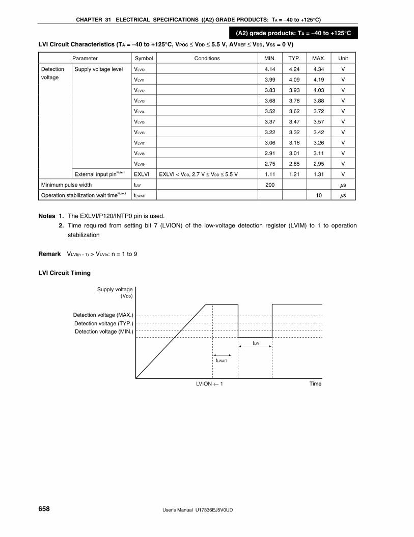
CHAPTER 31 ELECTRICAL SPECIFICATIONS ((A2) GRADE PRODUCTS: TA = −40 to +125°C)
User’s Manual U17336EJ5V0UD 658
(A2) grade products: TA = −40 to +125°C
LVI Circuit Characteristics (TA = −40 to +125°C, VPOC ≤ VDD ≤ 5.5 V, AVREF ≤ VDD, VSS = 0 V)
Parameter Symbol Conditions MIN. TYP. MAX. Unit
VLVI0 4.14 4.24 4.34 V
VLVI1 3.99 4.09 4.19 V
VLVI2 3.83 3.93 4.03 V
VLVI3 3.68 3.78 3.88 V
VLVI4 3.52 3.62 3.72 V
VLVI5 3.37 3.47 3.57 V
VLVI6 3.22 3.32 3.42 V
VLVI7 3.06 3.16 3.26 V
VLVI8 2.91 3.01 3.11 V
Supply voltage level
VLVI9 2.75 2.85 2.95 V
Detection
voltage
External input pinNote 1 EXLVI EXLVI < VDD, 2.7 V ≤ VDD ≤ 5.5 V 1.11 1.21 1.31 V
Minimum pulse width tLW 200 μs
Operation stabilization wait timeNote 2 tLWAIT 10 μs
Notes 1. The EXLVI/P120/INTP0 pin is used.
2. Time required from setting bit 7 (LVION) of the low-voltage detection register (LVIM) to 1 to operation
stabilization
Remark VLVI(n − 1) > VLVIn: n = 1 to 9
LVI Circuit Timing
Supply voltage
(VDD)
Time
Detection voltage (MIN.)
Detection voltage (TYP.)
Detection voltage (MAX.)
tLW
tLWAIT
LVION ← 1

CHAPTER 31 ELECTRICAL SPECIFICATIONS ((A2) GRADE PRODUCTS: TA = −40 to +125°C)
User’s Manual U17336EJ5V0UD 659
(A2) grade products: TA = −40 to +125°C
Data Memory STOP Mode Low Supply Voltage Data Retention Characteristics (TA = −40 to +125°C)
Parameter Symbol Conditions MIN. TYP. MAX. Unit
Data retention supply voltage VDDDR 1.44Note 5.5 V
Note The value depends on the POC detection voltage. When the voltage drops, the data is retained until a POC
reset is effected, but data is not retained when a POC reset is effected.
VDD
STOP instruction execution
Standby release signal(interrupt request)
STOP mode
Data retention mode
VDDDR
Operation mode
Flash Memory Programming Characteristics
(TA = −40 to +125°C, 2.7 V ≤ VDD ≤ 5.5 V, AVREF ≤ VDD, VSS = AVSS = 0 V)
• Basic characteristics
Parameter Symbol Conditions MIN. TYP. MAX. Unit
VDD supply current IDD fXP = 10 MHz (TYP.), 20 MHz (MAX.) 4.5 16.0 mA
All block Teraca 20 200 ms Erase timeNotes 1, 2
Block unit Terasa 20 200 ms
Write time (in 8-bit units)Note 1 Twrwa 10 100 μs
Number of rewrites per chip Cerwr Retention: 15 years
1 erase + 1 write after erase = 1 rewriteNote 3
100 Times
Notes 1. Characteristic of the flash memory. For the characteristic when a dedicated flash memory programmer,
PG-FP4, is used and the rewrite time during self programming, see Tables 25-12 and 25-13.
2. The prewrite time before erasure and the erase verify time (writeback time) are not included.
3. When a product is first written after shipment, “erase → write” and “write only” are both taken as one
rewrite.
Remarks 1. fXP: Main system clock oscillation frequency
2. For serial write operation characteristics, refer to 78K0/Kx2 Flash Memory Programming
(Programmer) Application Note (U17739E).
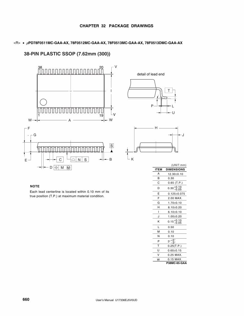
User’s Manual U17336EJ5V0UD 660
CHAPTER 32 PACKAGE DRAWINGS
• μPD78F0511MC-GAA-AX, 78F0512MC-GAA-AX, 78F0513MC-GAA-AX, 78F0513DMC-GAA-AX
2038
1
M
S
S
V
38-PIN PLASTIC SSOP (7.62mm (300))
detail of lead end
NOTE
Each lead centerline is located within 0.10 mm of its true position (T.P.) at maximum material condition.
ITEM DIMENSIONS
A
B
C
E
F
G
H
I
J
L
M
N
D
0.30
0.65 (T.P.)
0.125±0.075
2.00 MAX.
1.70±0.10
8.10±0.20
6.10±0.10
1.00±0.20
0.50
0.10
0.10
0.30+0.10−0.05
K 0.15+0.10−0.05
P 3°+5°−3°
(UNIT:mm)
P38MC-65-GAA
V
W WA
I
F
G
E C N
D M
B K
H
J
P
U
T
L
12.30±0.10
T
U
V
0.25(T.P.)
0.60±0.15
0.25 MAX.
W 0.15 MAX.
19
<R>
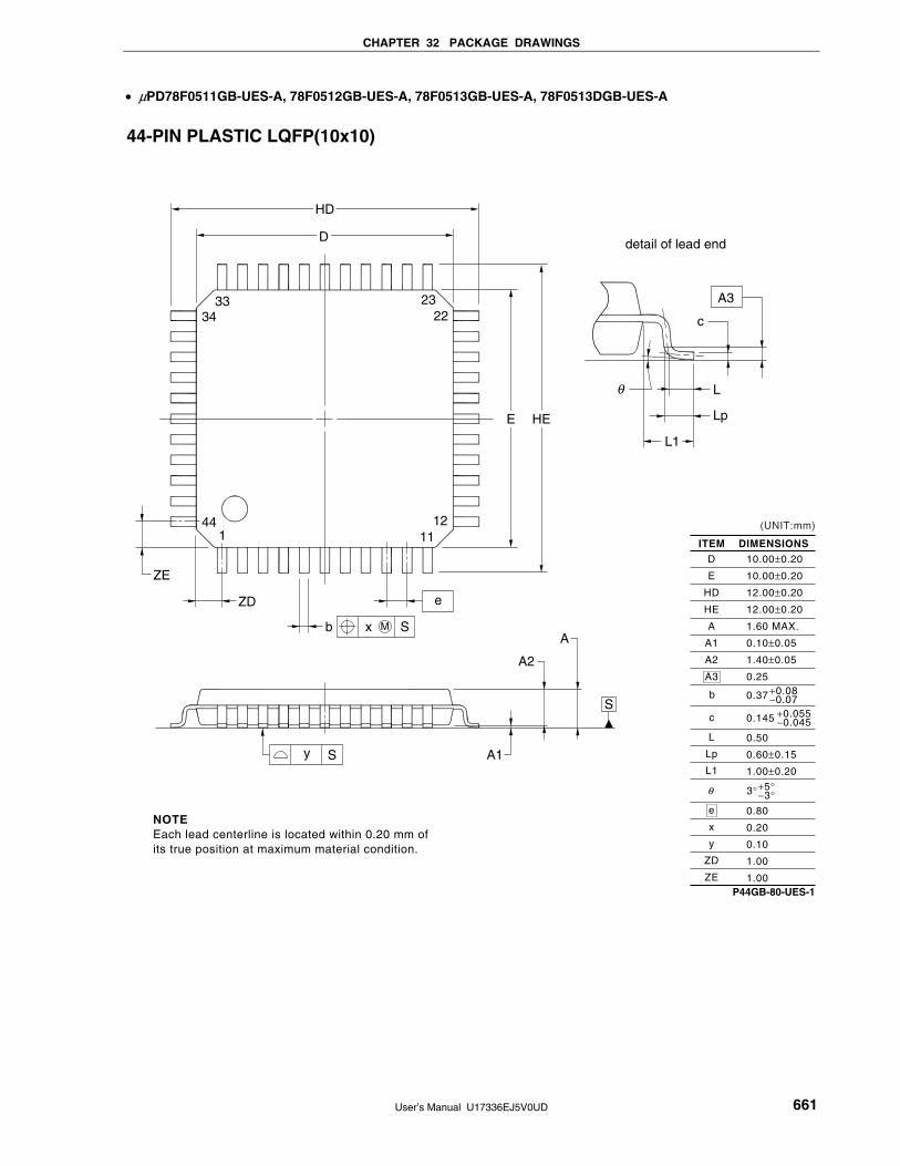
CHAPTER 32 PACKAGE DRAWINGS
User’s Manual U17336EJ5V0UD 661
• μPD78F0511GB-UES-A, 78F0512GB-UES-A, 78F0513GB-UES-A, 78F0513DGB-UES-A
Sy
e
Sxb M
θ L
c
Lp
HD
HE
ZD
ZE
L1
A1
A2
A
D
E
A3
S0.145 +0.055
−0.045
(UNIT:mm)
ITEM DIMENSIONS
D
E
HD
HE
A
A1
A2
A3
10.00±0.20
10.00±0.20
12.00±0.20
12.00±0.20
1.60 MAX.
0.10±0.05
1.40±0.05
0.25
c
θ
e
x
y
ZD
ZE
0.80
0.20
0.10
1.00
1.00
L
Lp
L1
0.50
0.60±0.15
1.00±0.20
P44GB-80-UES-1
3°+5°−3°
NOTEEach lead centerline is located within 0.20 mm ofits true position at maximum material condition.
detail of lead end
44-PIN PLASTIC LQFP(10x10)
0.37 +0.08−0.07b
11
22
144 12
2334
33

CHAPTER 32 PACKAGE DRAWINGS
User’s Manual U17336EJ5V0UD 662
• μPD78F0511GB(A)-GAF-AX, 78F0512GB(A)-GAF-AX, 78F0513GB(A)-GAF-AX, 78F0511GB(A2)-GAF-AX,
78F0512GB(A2)-GAF-AX, 78F0513GB(A2)-GAF-AX
Sy
e
Sxb M
θ L
c
Lp
HD
HE
ZD
ZE
L1
A1
A2
A
D
E
A3
S 0.125 +0.075−0.025
(UNIT:mm)
ITEM DIMENSIONS
D
E
HD
HE
A
A1
A2
A3
10.00±0.20
10.00±0.20
12.00±0.20
12.00±0.20
1.60 MAX.
0.10±0.05
1.40±0.05
0.25
c
θ
e
x
y
ZD
ZE
0.80
0.20
0.10
1.00
1.00
L
Lp
L1
0.50
0.60±0.15
1.00±0.20
P44GB-80-GAF
3°+5°−3°
NOTEEach lead centerline is located within 0.20 mm ofits true position at maximum material condition.
detail of lead end
44-PIN PLASTIC LQFP (10x10)
0.35 +0.08−0.04b
11
22
44 12
2334
33
1
<R>

CHAPTER 32 PACKAGE DRAWINGS
User’s Manual U17336EJ5V0UD 663
• μPD78F0511GA-8EU-A, 78F0512GA-8EU-A, 78F0513GA-8EU-A, 78F0514GA-8EU-A, 78F0515GA-8EU-A,
78F0515DGA-8EU-A
Sy
e
Sxb M
θ L
c
Lp
HD
HE
ZD
ZE
L1
A1
A2
A
D
E
A3
S 0.145 +0.055−0.045
(UNIT:mm)
ITEM DIMENSIONS
D
E
HD
HE
A
A1
A2
A3
7.00±0.20
7.00±0.20
9.00±0.20
9.00±0.20
1.60 MAX.
0.10±0.05
1.40±0.05
0.25
c
θ
e
x
y
ZD
ZE
0.50
0.08
0.08
0.75
0.75
L
Lp
L1
0.50
0.60±0.15
1.00±0.20
P48GA-50-8EU
3°+5°−3°
NOTEEach lead centerline is located within 0.08 mm ofits true position at maximum material condition.
detail of lead end
48-PIN PLASTIC LQFP (FINE PITCH)(7x7)
0.22±0.05b
12
24
1
48 13
2537
36

CHAPTER 32 PACKAGE DRAWINGS
User’s Manual U17336EJ5V0UD 664
• μPD78F0511GA(A)-GAM-AX, 78F0512GA(A)-GAM-AX, 78F0513GA(A)-GAM-AX, 78F0514GA(A)-GAM-AX,
78F0515GA(A)-GAM-AX, 78F0511GA(A2)-GAM-AX, 78F0512GA(A2)-GAM-AX, 78F0513GA(A2)-GAM-AX,
78F0514GA(A2)-GAM-AX, 78F0515GA(A2)-GAM-AX
48-PIN PLASTIC LQFP (FINE PITCH) (7x7)
Sy
e
Sxb M
θ L
c
Lp
HD
HE
ZD
ZE
L1
A1
A2
A
D
E
A3
S
0.125 +0.075−0.025
(UNIT:mm)
ITEM DIMENSIONS
D
E
HD
HE
A
A1
A2
A3
7.00±0.20
7.00±0.20
9.00±0.20
9.00±0.20
1.60 MAX.
0.10±0.05
1.40±0.05
0.25
c
θ
e
x
y
ZD
ZE
0.50
0.08
0.08
0.75
0.75
L
Lp
L1
0.50
0.60±0.15
1.00±0.20
P48GA-50-GAM
3°+5°−3°
NOTEEach lead centerline is located within 0.08 mm ofits true position at maximum material condition.
detail of lead end
0.20b
12
24
1
48 13
25
37
36
+0.07−0.03
<R>

User’s Manual U17336EJ5V0UD 665
CHAPTER 33 RECOMMENDED SOLDERING CONDITIONS
These products should be soldered and mounted under the following recommended conditions.
For soldering methods and conditions other than those recommended below, please contact an NEC Electronics
sales representative.
For technical information, see the following website.
Semiconductor Device Mount Manual (http://www.necel.com/pkg/en/mount/index.html)
Remark Evaluation of the soldering conditions for the 38-pin products is incomplete because these products are
under development.
Table 33-1. Surface Mounting Type Soldering Conditions
• 48-pin plastic LQFP (fine pitch) (7 × 7)
μPD78F0511GA-8EU-A, 78F0512GA-8EU-A, 78F0513GA-8EU-A, 78F0514GA-8EU-A, 78F0515GA-8EU-A,
78F0515DGA-8EU-ANote 1

User’s Manual U17336EJ5V0UD 666
CHAPTER 34 CAUTIONS FOR WAIT
34.1 Cautions for Wait
This product has two internal system buses.
One is a CPU bus and the other is a peripheral bus that interfaces with the low-speed peripheral hardware.
Because the clock of the CPU bus and the clock of the peripheral bus are asynchronous, unexpected illegal data
may be passed if an access to the CPU conflicts with an access to the peripheral hardware.
When accessing the peripheral hardware that may cause a conflict, therefore, the CPU repeatedly executes
processing, until the correct data is passed.
As a result, the CPU does not start the next instruction processing but waits. If this happens, the number of
execution clocks of an instruction increases by the number of wait clocks (for the number of wait clocks, see Table 34-
1). This must be noted when real-time processing is performed.

CHAPTER 34 CAUTIONS FOR WAIT
User’s Manual U17336EJ5V0UD 667
34.2 Peripheral Hardware That Generates Wait
Table 34-1 lists the registers that issue a wait request when accessed by the CPU, and the number of CPU wait
clocks.
Table 34-1. Registers That Generate Wait and Number of CPU Wait Clocks
Peripheral
Hardware
Register Access Number of Wait Clocks
Serial interface
UART0
ASIS0 Read 1 clock (fixed)
Serial interface
UART6
ASIS6 Read 1 clock (fixed)
Serial interface
IIC0
IICS0 Read 1 clock (fixed)
ADM Write
ADS Write
ADPC Write
ADCR Read
1 to 5 clocks (when fAD = fPRS/2 is selected)
1 to 7 clocks (when fAD = fPRS/3 is selected)
1 to 9 clocks (when fAD = fPRS/4 is selected)
2 to 13 clocks (when fAD = fPRS/6 is selected)
2 to 17 clocks (when fAD = fPRS/8 is selected)
2 to 25 clocks (when fAD = fPRS/12 is selected)
A/D converter
The above number of clocks is when the same source clock is selected for fCPU and fPRS. The number of wait
clocks can be calculated by the following expression and under the following conditions.
<Calculating number of wait clocks>
2 fCPU • Number of wait clocks = + 1
fAD * Fraction is truncated if the number of wait clocks ≤ 0.5 and rounded up if the number of wait clocks > 0.5.
fAD: A/D conversion clock frequency (fPRS/2 to fPRS/12)
fCPU: CPU clock frequency
fPRS: Peripheral hardware clock frequency
fXP: Main system clock frequency
<Conditions for maximum/minimum number of wait clocks>
• Maximum number of times: Maximum speed of CPU (fXP), lowest speed of A/D conversion clock (fPRS/12)
• Minimum number of times: Minimum speed of CPU (fSUB/2), highest speed of A/D conversion clock (fPRS/2)
Caution When the CPU is operating on the subsystem clock and the peripheral hardware clock is stopped,
do not access the registers listed above using an access method in which a wait request is issued.
Remark The clock is the CPU clock (fCPU).
User’s Manual U17336EJ5V0UD 668
APPENDIX A DEVELOPMENT TOOLS
The following development tools are available for the development of systems that employ the 78K0/KC2.
Figure A-1 shows the development tool configuration.
• Support for PC98-NX series
Unless otherwise specified, products supported by IBM PC/ATTM compatibles are compatible with PC98-NX
series computers. When using PC98-NX series computers, refer to the explanation for IBM PC/AT compatibles.
• WindowsTM
Unless otherwise specified, “Windows” means the following OSs.
• Windows 98
• Windows NTTM
• Windows 2000
• Windows XP

APPENDIX A DEVELOPMENT TOOLS
User’s Manual U17336EJ5V0UD 669
Figure A-1. Development Tool Configuration (1/3)
(1) When using the in-circuit emulator QB-78K0KX2
Language processing software
• Assembler package
• C compiler package
• Device fileNote 1
• C library source fileNote 2
Debugging software
• Integrated debuggerNote 4
• System simulator
Host machine(PC or EWS)
QB-78K0KX2Note 4
Emulation probe
Target system
Flash memoryprogrammer
Flash memorywrite adapter
Flash memory
• Software package
• Project manager
Software package
Flash memorywrite environment
Control software
(Windows only)Note 3
Power supply unitNote 4
USB interface cableNote 4
Notes 1. Download the device file for 78K0/KC2 (DF780547) from the download site for development tools
(http://www.necel.com/micro/ods/eng/index.html).
2. The C library source file is not included in the software package.
3. The project manager PM+ is included in the assembler package.
The PM+ is only used for Windows.
4. The QB-78K0KX2 is supplied with the integrated debugger ID78K0-QB, a USB interface cable, a
power supply unit, the on-chip debug emulator QB-MINI2, connection cables (10-pin and 16-pin
cables), and the 78K0-OCD board. Any other products are sold separately.
Download the software for operating the QB-MINI2 from the download site for development tools
(http://www.necel.com/micro/ods/eng/index.html) when using the QB-MINI2.
<R>
<R>

APPENDIX A DEVELOPMENT TOOLS
User’s Manual U17336EJ5V0UD 670
Figure A-1. Development Tool Configuration (2/3)
(2) When using the on-chip debug emulator QB-78K0MINI
Language processing software
• Assembler package
• C compiler package
• Device fileNote 1
• C library source fileNote 2
Debugging software
• Integrated debuggerNote 4
• System simulator
Host machine(PC or EWS)
USB interface cableNote 4
QB-78K0MININote 4
Connection cableNote 4
Target connector
Target system
Flash memory programmer
Flash memorywrite adapter
Flash memory
• Software package
• Project manager
Software package
Flash memorywrite environment
Control software
(Windows only)Note 3
Notes 1. Download the device file for 78K0/KC2 (DF780547) from the download site for development tools
(http://www.necel.com/micro/ods/eng/index.html).
2. The C library source file is not included in the software package. 3. The project manager PM+ is included in the assembler package.
The PM+ is only used for Windows.
4. The QB-78K0MINI is supplied with the integrated debugger ID78K0-QB, a USB interface cable, and a connection cable. Any other products are sold separately.
<R>

APPENDIX A DEVELOPMENT TOOLS
User’s Manual U17336EJ5V0UD 671
Figure A-1. Development Tool Configuration (3/3)
(3) When using the on-chip debug emulator with programming function QB-MINI2
QB-MINI2Note 4QB-MINI2Note 4
78K0-OCD boardNote 4
Language processing software
• Assembler package
• C compiler package
• Device fileNote 1
• C library source fileNote 2
Debugging software
• Integrated debuggerNote 1
• System simulator
Host machine(PC or EWS)
USB interface cableNote 4
Connection cable(10-pin/16-pin cable)Note 4
Target connector
Target system
Connection cable(16-pin cable)Note 4
• Software package
• Project manager
Software package
<When using as flash memory programmer>
Control software
(Windows only)Note 3
<When using as on-chip debug emulator>
Notes 1. Download the device file for 78K0/KC2 (DF780547) and the integrated debugger ID78K0-QB from the download site for development tools (http://www.necel.com/micro/ods/eng/index.html).
2. The C library source file is not included in the software package.
3. The project manager PM+ is included in the assembler package. The PM+ is only used for Windows.
4. The on-chip debug emulator QB-MINI2 is supplied with a USB interface cable, connection cables (10-
pin and 16–pin cables), and the 78K0-OCD board. Any other products are sold separately. Download the software for operating the QB-MINI2 from the download site for development tools
(http://www.necel.com/micro/ods/eng/index.html).
<R>
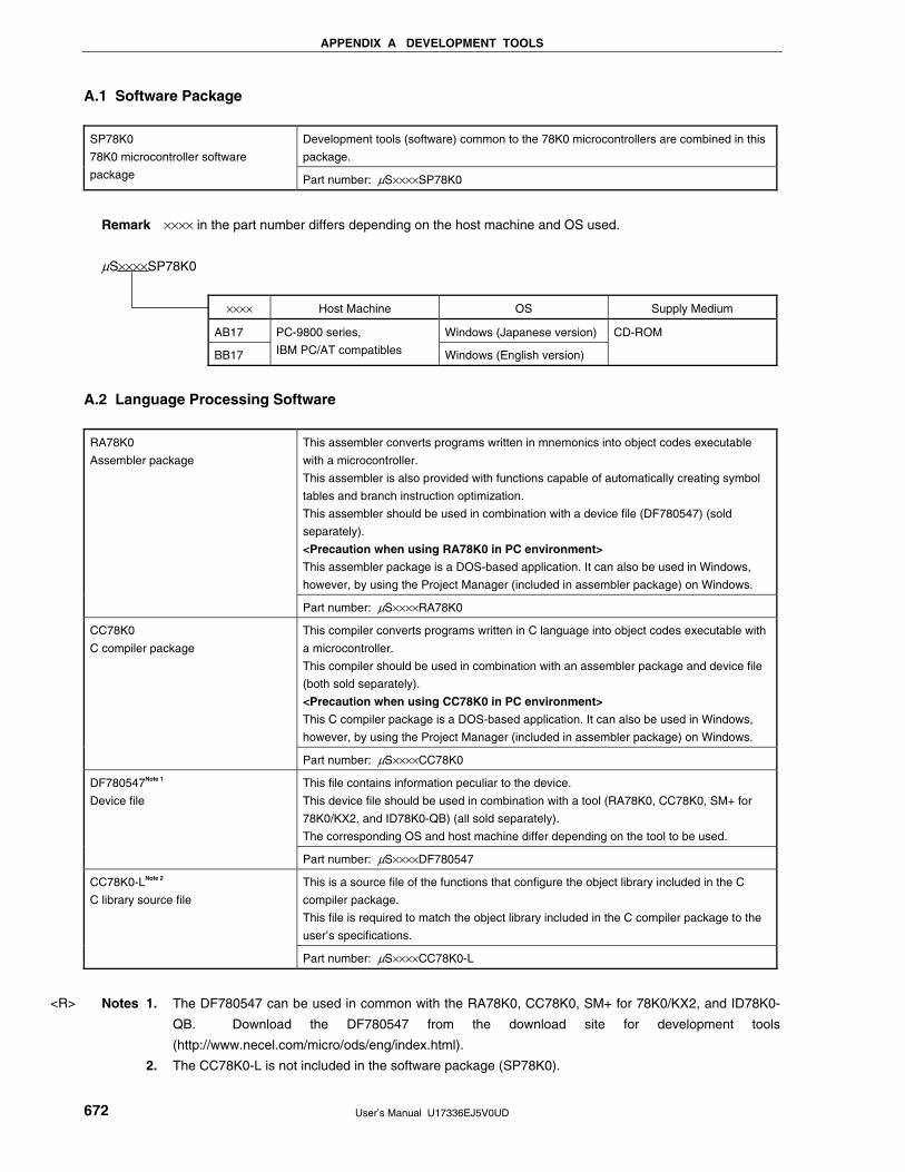
APPENDIX A DEVELOPMENT TOOLS
User’s Manual U17336EJ5V0UD 672
A.1 Software Package
Development tools (software) common to the 78K0 microcontrollers are combined in this
package.
SP78K0
78K0 microcontroller software
package Part number: μS××××SP78K0
Remark ×××× in the part number differs depending on the host machine and OS used.
μS××××SP78K0
×××× Host Machine OS Supply Medium
AB17 Windows (Japanese version)
BB17
PC-9800 series,
IBM PC/AT compatibles Windows (English version)
CD-ROM
A.2 Language Processing Software
This assembler converts programs written in mnemonics into object codes executable
with a microcontroller.
This assembler is also provided with functions capable of automatically creating symbol
tables and branch instruction optimization.
This assembler should be used in combination with a device file (DF780547) (sold
separately).
<Precaution when using RA78K0 in PC environment>
This assembler package is a DOS-based application. It can also be used in Windows,
however, by using the Project Manager (included in assembler package) on Windows.
RA78K0
Assembler package
Part number: μS××××RA78K0
This compiler converts programs written in C language into object codes executable with
a microcontroller.
This compiler should be used in combination with an assembler package and device file
(both sold separately).
<Precaution when using CC78K0 in PC environment>
This C compiler package is a DOS-based application. It can also be used in Windows,
however, by using the Project Manager (included in assembler package) on Windows.
CC78K0
C compiler package
Part number: μS××××CC78K0
This file contains information peculiar to the device.
This device file should be used in combination with a tool (RA78K0, CC78K0, SM+ for
78K0/KX2, and ID78K0-QB) (all sold separately).
The corresponding OS and host machine differ depending on the tool to be used.
DF780547Note 1
Device file
Part number: μS××××DF780547
This is a source file of the functions that configure the object library included in the C
compiler package.
This file is required to match the object library included in the C compiler package to the
user’s specifications.
CC78K0-LNote 2
C library source file
Part number: μS××××CC78K0-L
Notes 1. The DF780547 can be used in common with the RA78K0, CC78K0, SM+ for 78K0/KX2, and ID78K0-
QB. Download the DF780547 from the download site for development tools
(http://www.necel.com/micro/ods/eng/index.html).
2. The CC78K0-L is not included in the software package (SP78K0).
<R>

APPENDIX A DEVELOPMENT TOOLS
User’s Manual U17336EJ5V0UD 673
Remark ×××× in the part number differs depending on the host machine and OS used.
μS××××RA78K0
μS××××CC78K0
μS××××CC78K0-L
×××× Host Machine OS Supply Medium
AB17 Windows (Japanese version)
BB17
PC-9800 series,
IBM PC/AT compatibles Windows (English version)
3P17 HP9000 series 700TM HP-UXTM (Rel. 10.10)
3K17 SPARCstationTM SunOSTM (Rel. 4.1.4)
SolarisTM (Rel. 2.5.1)
CD-ROM
μS××××DF780547
×××× Host Machine OS Supply Medium
AB13 Windows (Japanese version)
BB13
PC-9800 series,
IBM PC/AT compatibles Windows (English version)
3.5-inch 2HD FD
A.3 Control Software
PM+
Project manager
This is control software designed to enable efficient user program development in the
Windows environment. All operations used in development of a user program, such as
starting the editor, building, and starting the debugger, can be performed from the project
manager.
<Caution>
The project manager is included in the assembler package (RA78K0).
It can only be used in Windows.

APPENDIX A DEVELOPMENT TOOLS
User’s Manual U17336EJ5V0UD 674
A.4 Flash Memory Writing Tools
A.4.1 When using flash memory programmer PG-FP4, FL-PR4, PG-FPL3, and FP-LITE3
PG-FP4, FL-PR4
Flash memory programmer
Flash memory programmer dedicated to microcontrollers with on-chip flash memory.
PG-FPL3, FP-LITE3
Simple flash memory programmer
Simple flash memory programmer dedicated to microcontrollers with on-chip flash
memory.
FA-78F0515GA-8EU-MX
FA-78F0513GB-UES-MX
FA-44GB-8ES-A
Flash memory writing adapter
Flash memory writing adapter used connected to the flash memory programmer.
• FA-78F0515GA-8EU-MX:
For 48-pin plastic LQFP (GA-8EU, GA-GAM type)
• FA-78F0513GB-UES-MX, FA-44GB-8ES-A:
For 44-pin plastic LQFP (GB-UES, GB-GAF type)
Remarks 1. FL-PR4, FP-LITE3, FA-78F0515GA-8EU-MX, FA-78F0513GB-UES-MX, and FA-44GB-8ES-A are
products of Naito Densei Machida Mfg. Co., Ltd.
TEL: +81-42-750-4172 Naito Densei Machida Mfg. Co., Ltd.
2. Use the latest version of the flash memory programming adapter.
A.4.2 When using on-chip debug emulator with programming function QB-MINI2
QB-MINI2
On-chip debug emulator with
programming function
This is a flash memory programmer dedicated to microcontrollers with on-chip flash
memory. It is available also as on-chip debug emulator which serves to debug hardware
and software when developing application systems using the 78K0/Kx2. When using this
as flash memory programmer, it should be used in combination with a connection cable
(16-pin cable) and a USB interface cable that is used to connect the host machine.
Target connector specifications 16-pin general-purpose connector (2.54 mm pitch)
Remarks 1. The QB-MINI2 is supplied with a USB interface cable, connection cables (10-pin and 16-pin cables),
and the 78K0-OCD board. The connection cable (10-pin cable) and the 78K0-OCD board are used
only when using the on-chip debug function.
2. Download the software for operating the QB-MINI2 from the download site for development tools
(http://www.necel.com/micro/ods/eng/index.html).
<R>

APPENDIX A DEVELOPMENT TOOLS
User’s Manual U17336EJ5V0UD 675
A.5 Debugging Tools (Hardware)
A.5.1 When using in-circuit emulator QB-78K0KX2
QB-78K0KX2
In-circuit emulator
This in-circuit emulator serves to debug hardware and software when developing application systems using the 78K0/Kx2. It supports to the integrated debugger (ID78K0-QB). This emulator should be used in combination with a power supply unit and emulation probe, and the USB is
used to connect this emulator to the host machine.
QB-144-CA-01 Check pin adapter
This check pin adapter is used in waveform monitoring using the oscilloscope, etc.
QB-80-EP-01T
Emulation probe
This emulation probe is flexible type and used to connect the in-circuit emulator and target
system.
QB-38MC-EA-01TNote, QB-44GB-EA-03T, QB-48GA-EA-02T
Exchange adapter
This exchange adapter is used to perform pin conversion from the in-circuit emulator to target connector. • QB-38MC-EA-01T: For 38-pin plastic SSOP (MC-GAA type) • QB-44GB-EA-03T: For 44-pin plastic LQFP (GB-UES, GB-GAF type) • QB-48GA-EA-02T: For 48-pin plastic LQFP (GA-8EU, GA-GAM type)
QB-38MC-YS-01TNote, QB-44GB-YS-01T, QB-48GA-YS-01T Space adapter
This space adapter is used to adjust the height between the target system and in-circuit emulator.• QB-38MC-YS-01T: For 38-pin plastic SSOP (MC-GAA type) • QB-44GB-YS-01T: For 44-pin plastic LQFP (GB-UES, GB-GAF type) • QB-48GA-YS-01T: For 48-pin plastic LQFP (GA-8EU, GA-GAM type)
QB-38MC-YQ-01TNote, QB-44GB-YQ-01T, QB-48GA-YQ-01T YQ connector
This YQ connector is used to connect the target connector and exchange adapter. • QB-38MC-YQ-01T: For 38-pin plastic SSOP (MC-GAA type) • QB-44GB-YQ-01T: For 44-pin plastic LQFP (GB-UES, GB-GAF type) • QB-48GA-YQ-01T: For 48-pin plastic LQFP (GA-8EU, GA-GAM type)
QB-38MC-HQ-01TNote, QB-44GB-HQ-01T, QB-48GA-HQ-01T Mount adapter
This mount adapter is used to mount the target device with socket. • QB-38MC-HQ-01T: For 38-pin plastic SSOP (MC-GAA type) • QB-44GB-HQ-01T: For 44-pin plastic LQFP (GB-UES, GB-GAF type) • QB-48GA-HQ-01T: For 48-pin plastic LQFP (GA-8EU, GA-GAM type)
QB-38MC-NQ-01TNote, QB-44GB-NQ-01T, QB-48GA-NQ-01T Target connector
This target connector is used to mount on the target system. • QB-38MC-NQ-01T: For 38-pin plastic SSOP (MC-GAA type) • QB-44GB-NQ-01T: For 44-pin plastic LQFP (GB-UES, GB-GAF type) • QB-48GA-NQ-01T: For 48-pin plastic LQFP (GA-8EU, GA-GAM type)
Remarks 1. The QB-78K0KX2 is supplied with the integrated debugger ID78K0-QB, a USB interface cable, a
power supply unit, the on-chip debug emulator QB-MINI2, connection cables (10-pin and 16-pin
cables), and the 78K0-OCD board.
Download the software for operating the QB-MINI2 from the download site for development tools
(http://www.necel.com/micro/ods/eng/index.html) when using the QB-MINI2.
2. The packed contents differ depending on the part number, as follows.
Packed Contents
Part Number
In-Circuit Emulator Emulation Probe Exchange Adapter YQ Connector Target Connector
QB-78K0KX2-ZZZ None
QB-78K0KX2-T44GB QB-44GB-EA-03T QB-44GB-YQ-01T QB-44GB-NQ-01T
QB-78K0KX2-T48GA QB-48GA-EA-02T QB-48GA-YQ-01T QB-48GA-NQ-01T
QB-78K0KX2-T38MCNote
QB-78K0KX2
QB-80-EP-01T
QB-38MC-EA-01TNote QB-38MC-YQ-01TNote QB-38MC-NQ-01TNote
Note Under development
<R>
<R>
<R>
<R>
<R>
<R>
<R>

APPENDIX A DEVELOPMENT TOOLS
User’s Manual U17336EJ5V0UD 676
A.5.2 When using on-chip debug emulator QB-78K0MINI
QB-78K0MINI On-chip debug emulator
This on-chip debug emulator serves to debug hardware and software when developing application systems using the 78K0/Kx2. It supports the integrated debugger (ID78K0-QB). This emulator should be used in combination with a connection cable and a USB interface cable that is used to connect the host machine.
Target connector specifications
10-pin general-purpose connector (2.54 mm pitch)
Remark The QB-78K0MINI is supplied with a USB interface cable, connection cables, and the integrated
debugger ID78K0-QB.
A.5.3 When using on-chip debug emulator with programming function QB-MINI2
QB-MINI2 On-chip debug emulator with
programming function
This on-chip debug emulator serves to debug hardware and software when developing application systems using the 78K0/Kx2. It is available also as flash memory programmer dedicated to microcontrollers with on-chip flash memory. When using this as on-chip debug emulator, it should be used in combination with a connection cable (10-pin cable or 16-pin cable), a USB interface cable that is used to connect the host machine, and the 78K0-OCD board.
Target connector specifications
10-pin general-purpose connector (2.54 mm pitch) or 16-pin general-purpose connector (2.54 mm pitch)
Remarks 1. The QB-MINI2 is supplied with a USB interface cable, connection cables (10-pin and 16-pin cables),
and the 78K0-OCD board. The connection cable (10-pin cable) and the 78K0-OCD board are used
only when using the on-chip debug function.
2. Download the software for operating the QB-MINI2 from the download site for development tools
(http://www.necel.com/micro/ods/eng/index.html).
<R>
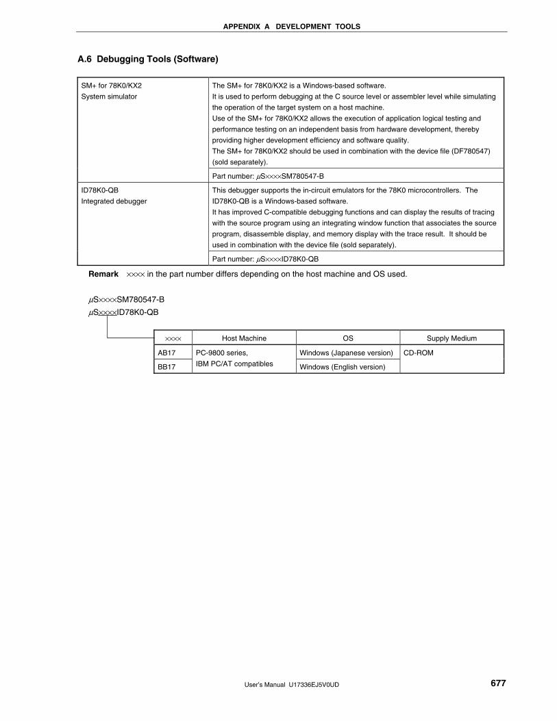
APPENDIX A DEVELOPMENT TOOLS
User’s Manual U17336EJ5V0UD 677
A.6 Debugging Tools (Software)
The SM+ for 78K0/KX2 is a Windows-based software.
It is used to perform debugging at the C source level or assembler level while simulating
the operation of the target system on a host machine.
Use of the SM+ for 78K0/KX2 allows the execution of application logical testing and
performance testing on an independent basis from hardware development, thereby
providing higher development efficiency and software quality.
The SM+ for 78K0/KX2 should be used in combination with the device file (DF780547)
(sold separately).
SM+ for 78K0/KX2
System simulator
Part number: μS××××SM780547-B
This debugger supports the in-circuit emulators for the 78K0 microcontrollers. The
ID78K0-QB is a Windows-based software.
It has improved C-compatible debugging functions and can display the results of tracing
with the source program using an integrating window function that associates the source
program, disassemble display, and memory display with the trace result. It should be
used in combination with the device file (sold separately).
ID78K0-QB
Integrated debugger
Part number: μS××××ID78K0-QB
Remark ×××× in the part number differs depending on the host machine and OS used.
μS××××SM780547-B
μS××××ID78K0-QB
×××× Host Machine OS Supply Medium
AB17 Windows (Japanese version)
BB17
PC-9800 series,
IBM PC/AT compatibles Windows (English version)
CD-ROM

User’s Manual U17336EJ5V0UD 678
APPENDIX B NOTES ON TARGET SYSTEM DESIGN
This chapter shows areas on the target system where component mounting is prohibited and areas where there
are component mounting height restrictions when the QB-78K0KX2 is used.
Figure B-1. For 44-Pin GB Package
15
9.85
13.375
10
15
9.85
17.375
10
: Exchange adapter area: Components up to 17.45 mm in height can be mountedNote
: Emulation probe tip area: Components up to 24.45 mm in height can be mounted Note
Note Height can be adjusted by using space adapters (each adds 2.4 mm)

APPENDIX B NOTES ON TARGET SYSTEM DESIGN
User’s Manual U17336EJ5V0UD 679
Figure B-2. For 48-Pin GA Package
15
9.5
13.375
10
15
9.5
17.375
10
: Exchange adapter area: Components up to 17.45 mm in height can be mountedNote
: Emulation probe tip area: Components up to 24.45 mm in height can be mounted Note
Note Height can be adjusted by using space adapters (each adds 2.4 mm)

User’s Manual U17336EJ5V0UD 680
APPENDIX C REGISTER INDEX
C.1 Register Index (In Alphabetical Order with Respect to Register Names)
[A]
A/D converter mode register (ADM) ............................................................................................................................287
A/D port configuration register (ADPC) ...............................................................................................................115, 293
Analog input channel specification register (ADS) ......................................................................................................292
Asynchronous serial interface control register 6 (ASICL6)..........................................................................................340
Asynchronous serial interface operation mode register 0 (ASIM0) .............................................................................310
Asynchronous serial interface operation mode register 6 (ASIM6) .............................................................................334
Asynchronous serial interface reception error status register 0 (ASIS0) .....................................................................312
Asynchronous serial interface reception error status register 6 (ASIS6) .....................................................................336
Asynchronous serial interface transmission status register 6 (ASIF6) ........................................................................337
[B]
Baud rate generator control register 0 (BRGC0) .........................................................................................................313
Baud rate generator control register 6 (BRGC6) .........................................................................................................339
[C]
Capture/compare control register 00 (CRC00)............................................................................................................165
Clock operation mode select register (OSCCTL) ........................................................................................................123
Clock output selection register (CKS) .........................................................................................................................281
Clock selection register 6 (CKSR6).............................................................................................................................337
[E]
8-bit A/D conversion result register (ADCRH) .............................................................................................................291
8-bit timer compare register 50 (CR50).......................................................................................................................226
8-bit timer compare register 51 (CR51).......................................................................................................................226
8-bit timer counter 50 (TM50)......................................................................................................................................226
8-bit timer counter 51 (TM51)......................................................................................................................................226
8-bit timer H carrier control register 1 (TMCYC1)........................................................................................................249
8-bit timer H compare register 00 (CMP00).................................................................................................................244
8-bit timer H compare register 01 (CMP01).................................................................................................................244
8-bit timer H compare register 10 (CMP10).................................................................................................................244
8-bit timer H compare register 11 (CMP11).................................................................................................................244
8-bit timer H mode register 0 (TMHMD0) ....................................................................................................................245
8-bit timer H mode register 1 (TMHMD1) ....................................................................................................................245
8-bit timer mode control register 50 (TMC50)..............................................................................................................229
8-bit timer mode control register 51 (TMC51)..............................................................................................................229
External interrupt falling edge enable register (EGN)..................................................................................................472
External interrupt rising edge enable register (EGP)...................................................................................................472
[I]
IIC clock selection register 0 (IICCL0).........................................................................................................................397
IIC control register 0 (IICC0) .......................................................................................................................................388

APPENDIX C REGISTER INDEX
User’s Manual U17336EJ5V0UD 681
IIC flag register 0 (IICF0) ............................................................................................................................................395
IIC function expansion register 0 (IICX0) ....................................................................................................................398
IIC shift register 0 (IIC0)..............................................................................................................................................385
IIC status register 0 (IICS0) ........................................................................................................................................393
Input switch control register (ISC) ...............................................................................................................................342
Internal expansion RAM size switching register (IXS).................................................................................................536
Internal memory size switching register (IMS) ............................................................................................................535
Internal oscillation mode register (RCM).....................................................................................................................127
Interrupt mask flag register 0H (MK0H) ......................................................................................................................470
Interrupt mask flag register 0L (MK0L)........................................................................................................................470
Interrupt mask flag register 1H (MK1H) ......................................................................................................................470
Interrupt mask flag register 1L (MK1L)........................................................................................................................470
Interrupt request flag register 0H (IF0H) .....................................................................................................................468
Interrupt request flag register 0L (IF0L) ......................................................................................................................468
Interrupt request flag register 1H (IF1H) .....................................................................................................................468
Interrupt request flag register 1L (IF1L) ......................................................................................................................468
[K]
Key return mode register (KRM) .................................................................................................................................482
[L]
Low-voltage detection level selection register (LVIS)..................................................................................................515
Low-voltage detection register (LVIM) ........................................................................................................................513
[M]
Main clock mode register (MCM) ................................................................................................................................129
Main OSC control register (MOC) ...............................................................................................................................128
Multiplication/division data register A0 (MDA0H, MDA0L) ..........................................................................................455
Multiplication/division data register B0 (MDB0)...........................................................................................................456
Multiplier/divider control register 0 (DMUC0) ..............................................................................................................457
[O]
Oscillation stabilization time counter status register (OSTC) ..............................................................................130, 484
Oscillation stabilization time select register (OSTS)............................................................................................131, 485
[P]
Port mode register 0 (PM0).................................................................................................................................111, 170
Port mode register 1 (PM1)................................................................................................. 111, 231, 250, 314, 342, 370
Port mode register 2 (PM2).................................................................................................................................111, 294
Port mode register 3 (PM3).................................................................................................................................111, 231
Port mode register 4 (PM4).........................................................................................................................................111
Port mode register 6 (PM6).................................................................................................................................111, 400
Port mode register 7 (PM7).........................................................................................................................................111
Port mode register 12 (PM12).............................................................................................................................111, 516
Port mode register 14 (PM14).............................................................................................................................111, 283
Port register 0 (P0)......................................................................................................................................................113
Port register 1 (P1)......................................................................................................................................................113
Port register 2 (P2)......................................................................................................................................................113

APPENDIX C REGISTER INDEX
User’s Manual U17336EJ5V0UD 682
Port register 3 (P3)......................................................................................................................................................113
Port register 4 (P4)......................................................................................................................................................113
Port register 6 (P6)......................................................................................................................................................113
Port register 7 (P7)......................................................................................................................................................113
Port register 12 (P12)..................................................................................................................................................113
Port register 13 (P13)..................................................................................................................................................113
Port register 14 (P14)..................................................................................................................................................113
Prescaler mode register 00 (PRM00)..........................................................................................................................168
Priority specification flag register 0H (PR0H) ..............................................................................................................471
Priority specification flag register 0L (PR0L) ...............................................................................................................471
Priority specification flag register 1H (PR1H) ..............................................................................................................471
Priority specification flag register 1L (PR1L) ...............................................................................................................471
Processor clock control register (PCC) .......................................................................................................................125
Pull-up resistor option register 0 (PU0) .......................................................................................................................114
Pull-up resistor option register 1 (PU1) .......................................................................................................................114
Pull-up resistor option register 3 (PU3) .......................................................................................................................114
Pull-up resistor option register 4 (PU4) .......................................................................................................................114
Pull-up resistor option register 7 (PU7) .......................................................................................................................114
Pull-up resistor option register 12 (PU12) ...................................................................................................................114
Pull-up resistor option register 14 (PU14) ...................................................................................................................114
[R]
Receive buffer register 0 (RXB0) ................................................................................................................................309
Receive buffer register 6 (RXB6) ................................................................................................................................333
Receive shift register 0 (RXS0) ...................................................................................................................................309
Receive shift register 6 (RXS6) ...................................................................................................................................333
Remainder data register 0 (SDR0)..............................................................................................................................455
Reset control flag register (RESF) ..............................................................................................................................505
[S]
Serial clock selection register 10 (CSIC10) .................................................................................................................368
Serial I/O shift register 10 (SIO10) ..............................................................................................................................366
Serial operation mode register 10 (CSIM10) ...............................................................................................................367
16-bit timer capture/compare register 000 (CR000) ....................................................................................................159
16-bit timer capture/compare register 010 (CR010) ....................................................................................................159
16-bit timer counter 00 (TM00)....................................................................................................................................159
16-bit timer mode control register 00 (TMC00)............................................................................................................163
16-bit timer output control register 00 (TOC00)...........................................................................................................166
Slave address register 0 (SVA0) .................................................................................................................................385
[T]
Timer clock selection register 50 (TCL50)...................................................................................................................227
Timer clock selection register 51 (TCL51)...................................................................................................................227
10-bit A/D conversion result register (ADCR)..............................................................................................................290
Transmit buffer register 10 (SOTB10) .........................................................................................................................366
Transmit buffer register 6 (TXB6)................................................................................................................................333
Transmit shift register 0 (TXS0) ..................................................................................................................................309

APPENDIX C REGISTER INDEX
User’s Manual U17336EJ5V0UD 683
Transmit shift register 6 (TXS6) ..................................................................................................................................333
[W]
Watch timer operation mode register (WTM) ..............................................................................................................269
Watchdog timer enable register (WDTE) ....................................................................................................................275
C.2 Register Index (In Alphabetical Order with Respect to Register Symbol)
[A]
ADCR: 10-bit A/D conversion result register .......................................................................................................290
ADCRH: 8-bit A/D conversion result register .........................................................................................................291
ADM: A/D converter mode register ...................................................................................................................287
ADPC: A/D port configuration register.........................................................................................................115, 293
ADS: Analog input channel specification register .............................................................................................292
ASICL6: Asynchronous serial interface control register 6......................................................................................340
ASIF6: Asynchronous serial interface transmission status register 6..................................................................337
ASIM0: Asynchronous serial interface operation mode register 0........................................................................310
ASIM6: Asynchronous serial interface operation mode register 6........................................................................334
ASIS0: Asynchronous serial interface reception error status register 0...............................................................312
ASIS6: Asynchronous serial interface reception error status register 6...............................................................336
[B]
BRGC0: Baud rate generator control register 0.....................................................................................................313
BRGC6: Baud rate generator control register 6.....................................................................................................339
[C]
CKS: Clock output selection register ................................................................................................................281
CKSR6: Clock selection register 6 ........................................................................................................................337
CMP00: 8-bit timer H compare register 00............................................................................................................244
CMP01: 8-bit timer H compare register 01............................................................................................................244
CMP10: 8-bit timer H compare register 10............................................................................................................244
CMP11: 8-bit timer H compare register 11............................................................................................................244
CR000: 16-bit timer capture/compare register 000...............................................................................................159
CR010: 16-bit timer capture/compare register 010...............................................................................................159
CR50: 8-bit timer compare register 50 ...............................................................................................................226
CR51: 8-bit timer compare register 51 ...............................................................................................................226
CRC00: Capture/compare control register 00.......................................................................................................165
CSIC10: Serial clock selection register 10.............................................................................................................368
CSIM10: Serial operation mode register 10 ...........................................................................................................367
[D]
DMUC0: Multiplier/divider control register 0...........................................................................................................457
[E]
EGN: External interrupt falling edge enable register .........................................................................................472
EGP: External interrupt rising edge enable register..........................................................................................472
[I]
IF0H: Interrupt request flag register 0H.............................................................................................................468

APPENDIX C REGISTER INDEX
User’s Manual U17336EJ5V0UD 684
IF0L: Interrupt request flag register 0L .............................................................................................................468
IF1H: Interrupt request flag register 1H.............................................................................................................468
IF1L: Interrupt request flag register 1L .............................................................................................................468
IIC0: IIC shift register 0 ....................................................................................................................................385
IICC0: IIC control register 0 ................................................................................................................................388
IICCL0: IIC clock selection register 0....................................................................................................................397
IICF0: IIC flag register 0 .....................................................................................................................................395
IICS0: IIC status register 0 .................................................................................................................................393
IICX0: IIC function expansion register 0 .............................................................................................................398
IMS: Internal memory size switching register...................................................................................................535
ISC: Input switch control register.....................................................................................................................342
IXS: Internal expansion RAM size switching register ......................................................................................536
[K]
KRM: Key return mode register .........................................................................................................................482
[L]
LVIM: Low-voltage detection register.................................................................................................................513
LVIS: Low-voltage detection level selection register .........................................................................................515
[M]
MCM: Main clock mode register.........................................................................................................................129
MDA0H: Multiplication/division data register A0.....................................................................................................455
MDA0L: Multiplication/division data register A0.....................................................................................................455
MDB0: Multiplication/division data register B0.....................................................................................................456
MK0H: Interrupt mask flag register 0H ................................................................................................................470
MK0L: Interrupt mask flag register 0L.................................................................................................................470
MK1H: Interrupt mask flag register 1H ................................................................................................................470
MK1L: Interrupt mask flag register 1L.................................................................................................................470
MOC: Main OSC control register .......................................................................................................................128
[O]
OSCCTL: Clock operation mode select register ......................................................................................................123
OSTC: Oscillation stabilization time counter status register ........................................................................130, 484
OSTS: Oscillation stabilization time select register .....................................................................................131, 485
[P]
P0: Port register 0..........................................................................................................................................113
P1: Port register 1..........................................................................................................................................113
P2: Port register 2..........................................................................................................................................113
P3: Port register 3..........................................................................................................................................113
P4: Port register 4..........................................................................................................................................113
P6: Port register 6..........................................................................................................................................113
P7: Port register 7..........................................................................................................................................113
P12: Port register 12........................................................................................................................................113
P13: Port register 13........................................................................................................................................113
P14: Port register 14........................................................................................................................................113
PCC: Processor clock control register...............................................................................................................125

APPENDIX C REGISTER INDEX
User’s Manual U17336EJ5V0UD 685
PM0: Port mode register 0........................................................................................................................111, 170
PM1: Port mode register 1........................................................................................ 111, 231, 250, 314, 342, 370
PM2: Port mode register 2........................................................................................................................111, 294
PM3: Port mode register 3........................................................................................................................111, 231
PM4: Port mode register 4................................................................................................................................111
PM6: Port mode register 6........................................................................................................................111, 400
PM7: Port mode register 7................................................................................................................................111
PM12: Port mode register 12......................................................................................................................111, 516
PM14: Port mode register 14......................................................................................................................111, 283
PR0H: Priority specification flag register 0H .......................................................................................................471
PR0L: Priority specification flag register 0L........................................................................................................471
PR1H: Priority specification flag register 1H .......................................................................................................471
PR1L: Priority specification flag register 1L........................................................................................................471
PRM00: Prescaler mode register 00 .....................................................................................................................168
PU0: Pull-up resistor option register 0..............................................................................................................114
PU1: Pull-up resistor option register 1..............................................................................................................114
PU3: Pull-up resistor option register 3..............................................................................................................114
PU4: Pull-up resistor option register 4..............................................................................................................114
PU7: Pull-up resistor option register 7..............................................................................................................114
PU12: Pull-up resistor option register 12............................................................................................................114
PU14: Pull-up resistor option register 14............................................................................................................114
[R]
RCM: Internal oscillation mode register.............................................................................................................127
RESF: Reset control flag register .......................................................................................................................505
RXB0: Receive buffer register 0 .........................................................................................................................309
RXB6: Receive buffer register 6 .........................................................................................................................333
RXS0: Receive shift register 0............................................................................................................................309
RXS6: Receive shift register 6............................................................................................................................333
[S]
SDR0: Remainder data register 0.......................................................................................................................455
SIO10: Serial I/O shift register 10........................................................................................................................366
SOTB10: Transmit buffer register 10 ......................................................................................................................366
SVA0: Slave address register 0..........................................................................................................................385
[T]
TCL50: Timer clock selection register 50.............................................................................................................227
TCL51: Timer clock selection register 51.............................................................................................................227
TM00: 16-bit timer counter 00 ............................................................................................................................159
TM50: 8-bit timer counter 50 ..............................................................................................................................226
TM51: 8-bit timer counter 51 ..............................................................................................................................226
TMC00: 16-bit timer mode control register 00.......................................................................................................163
TMC50: 8-bit timer mode control register 50.........................................................................................................229
TMC51: 8-bit timer mode control register 51.........................................................................................................229
TMCYC1: 8-bit timer H carrier control register 1 ......................................................................................................249
TMHMD0: 8-bit timer H mode register 0...................................................................................................................245

APPENDIX C REGISTER INDEX
User’s Manual U17336EJ5V0UD 686
TMHMD1: 8-bit timer H mode register 1 ...................................................................................................................245
TOC00: 16-bit timer output control register 00 ......................................................................................................166
TXB6: Transmit buffer register 6 ........................................................................................................................333
TXS0: Transmit shift register 0 ...........................................................................................................................309
TXS6: Transmit shift register 6 ...........................................................................................................................333
[W]
WDTE: Watchdog timer enable register...............................................................................................................275
WTM: Watch timer operation mode register.......................................................................................................269

User’s Manual U17336EJ5V0UD 687
APPENDIX D LIST OF CAUTIONS
This appendix lists cautions described in this document. “Classification (hard/soft)” in table is as follows.
Hard: Cautions for microcontroller internal/external hardware Soft: Cautions for software such as register settings or programs
(1/26)
Cha
pter
Cla
ssifi
catio
n Function Details of Function
Cautions Page
pp. AVSS Make AVSS the same potential as VSS.
20, 22, 24
pp. REGC Connect the REGC pin to VSS via a capacitor (0.47 to 1 μF: recommended).
20, 22, 24
ANI0/P20 to ANI5/P25 (38 pin products)
ANI0/P20 to ANI5/P25 are set in the analog input mode after release of reset. p. 20
pp.
Cha
pter
1
Har
d Pin function
ANI0/P20 to ANI7/P27
ANI0/P20 to ANI7/P27 are set in the analog input mode after release of reset.
22, 24, 38
Sof
t
P20 to P27 For the 38-pin products, be sure to set bits 6 and 7 of PM2 to “1”, and bits 6 and 7 of P2 to “0”.
p. 38
In the products with an on-chip debug function (μPD78F0513D and 78F0515D), be sure to pull the P31/INTP2/OCD1A pin down before a reset release, to prevent malfunction.
p. 39
Har
d P31/INTP2/ OCD1A
For products without an on-chip debug function, with the flash memory of 48 KB or more (μPD78F0514 and 78F0515), and having a product rank of “I”, “K”, or “E”, and for the products with an on-chip debug function (μPD78F0513D and 78F0515D), connect P31/INTP2/OCD1A as follows when writing the flash memory with a flash memory programmer. • P31/INTP2/OCD1A: Connect to VSS via a resistor (10 kΩ: recommended). The above connection is not necessary when writing the flash memory by means of self programming.
p. 39
P40, P41 For the 38-pin products, be sure to set bits 0 and 1 of PM4 and P4 to “0”. p. 39
Sof
t
P70 to P75 For the 38-pin products, be sure to set bits 2 and 3 of PM7 and P7 to “0”. p. 40
P121/X1 For products without an on-chip debug function, with the flash memory of 48 KB or more (μPD78F0514 and 78F0515), and having a product rank of “I”, “K”, or “E”, and for the product with an on-chip debug function (μPD78F0513D and 78F0515D), connect P121/X1/OCD0A as follows when writing the flash memory with a flash memory programmer. • P121/X1/OCD0A: When using this pin as a port, connect it to VSS via a resistor
(10 kΩ: recommended) (in the input mode) or leave it open (in the output mode).The above connection is not necessary when writing the flash memory by means of self programming.
p. 41
Cha
pter
2
Har
d
Pin function
REGC pin Keep the wiring length as short as possible for the broken-line part in the above figure.
p. 42
IMS, IXS: Internal memory size switching register, internal expansion RAM size switching register
Regardless of the internal memory capacity, the initial values of the internal memory size switching register (IMS) and internal expansion RAM size switching register (IXS) of all products in the 78K0/KC2 are fixed (IMS = CFH, IXS = 0CH). Therefore, set the value corresponding to each product as indicated below.
p. 47
SFR: Special function register
Do not access addresses to which SFRs are not assigned. p. 59
Cha
pter
3
Sof
t
Memory space
SP: Stack pointer
Since reset signal generation makes the SP contents undefined, be sure to initialize the SP before using the stack.
p. 66

APPENDIX D LIST OF CAUTIONS
User’s Manual U17336EJ5V0UD 688
(2/26) C
hapt
er
Cla
ssifi
catio
n Function Details of Function
Cautions Page S
oft
P10/SCK10/TxD0, P12/SO10
To use P10/SCK10/TxD0 and P12/SO10 as general-purpose ports, set serial operation mode register 10 (CSIM10) and serial clock selection register 10 (CSIC10) to the default status (00H).
p. 92
Har
d Make the AVREF pin the same potential as the VDD pin when port 2 is used as a digital port.
p. 97
Sof
t
Port 2
For the 38-pin products, be sure to set bits 6 and 7 of PM2 to “1”, and bits 6 and 7 of P2 to “0”.
p. 97
In the product with an on-chip debug function (μPD78F0513D and 78F0515D), be sure to pull the P31/INTP2/OCD1A pin down before a reset release, to prevent malfunction.
p. 99
Har
d P31/INTP2/ OCD1A
For products without an on-chip debug function, with the flash memory of 48 KB or more (μPD78F0514 and 78F0515), and having a product rank of “I”, “K”, or “E”, and for the products with an on-chip debug function (μPD78F0513D and 78F0515D), connect P31/INTP2/OCD1A as follows when writing the flash memory with a flash memory programmer. • P31/INTP2/OCD1A: Connect to VSS via a resistor (10 kΩ: recommended). The above connection is not necessary when writing the flash memory by means of self programming.
p. 99
Port 4 For the 38-pin products, be sure to set bits 0 and 1 of PM4 and P4 to “0”. p. 102
Port 7 For the 38-pin products, be sure to set bits 2 and 3 of PM7 and P7 to “0”. p. 105
Sof
t
When using the P121 to P124 pins to connect a resonator for the main system clock (X1, X2) or subsystem clock (XT1, XT2), or to input an external clock for the main system clock (EXCLK) or subsystem clock (EXCLKS), the X1 oscillation mode, XT1 oscillation mode, or external clock input mode must be set by using the clock operation mode select register (OSCCTL) (for details, see 5.3 (1) Clock operation mode select register (OSCCTL) and (3) Setting of operation mode for subsystem clock pin). The reset value of OSCCTL is 00H (all of the P121 to P124 pins are I/O port pins). At this time, setting of the PM121 to PM124 and P121 to P124 pins is not necessary.
p. 106
Har
d
P121/X1/OCD0A, P122/X2/EXCLK/OCD0B, P123/XT1, P124/XT2/EXCLKS
For products without an on-chip debug function, with the flash memory of 48 KB or more (μPD78F0514 and 78F0515), and having a product rank of “I”, “K”, or “E”, and for the product with an on-chip debug function (μPD78F0513D and 78F0515D), connect P121/X1/OCD0A as follows when writing the flash memory with a flash memory programmer. • P121/X1/OCD0A: When using this pin as a port, connect it to VSS via a resistor
(10 kΩ: recommended) (in the input mode) or leave it open (in the output mode).
The above connection is not necessary when writing the flash memory by means of self programming.
p. 106
PMm: Port mode registers
For the 38-pin products, be sure to set bits 2 to 7 of PM0, bits 6 and 7 of PM2, bits 4 to 7 of PM3, bits 2 to 7 of PM4, bits 4 to 7 of PM6, bits 4 to 7 of PM7, and bits 5 to 7 of PM12 to “1”. Also, be sure to set bits 0 and 1 of PM4, and bits 2 and 3 of PM7 to “0”. For the 44-pin products, be sure to set bits 2 to 7 of PM0, bits 4 to 7 of PM3, bits 2 to 7 of PM4, bits 4 to 7 of PM6, bits 4 to 7 of PM7, and bits 5 to 7 of PM12 to “1”. For the 48-pin products, be sure to set bits 2 to 7 of PM0, bits 4 to 7 of PM3, bits 2 to 7 of PM4, bits 4 to 7 of PM6, bits 6 and 7 of PM7, and bits 5 to 7 of PM12, and bits 1 to 7 of PM14 to “1”.
p. 112
Pm: Port register For the 38-pin products, be sure to set bits 6 and 7 of P2, bits 0 and 1 of P4, and bits 2 and 3 of P7 to “0”.
p. 113
Cha
pter
4
Sof
t
Port function
ADPC: A/D port configuration register
Set the channel used for A/D conversion to the input mode by using port mode register 2 (PM2).
p. 115

APPENDIX D LIST OF CAUTIONS
User’s Manual U17336EJ5V0UD 689
(3/26)
Cha
pter
Cla
ssifi
catio
n Function Details of Function
Cautions Page
If data is written to ADPC, a wait cycle is generated. Do not write data to ADPC when the CPU is operating on the subsystem clock and the peripheral hardware clock is stopped. For details, see CHAPTER 34 CAUTIONS FOR WAIT.
p. 115 ADPC: A/D port configuration register
For the 38-pin products, setting ADPC3, ADPC2, ADPC1, ADPC0 to 0, 1, 1, 1 or 1, 0, 0, 0 is prohibited.
p. 115
Cha
pter
4
Sof
t
Port function
1-bit manipulation instruction for port register n (Pn)
When a 1-bit manipulation instruction is executed on a port that provides both input and output functions, the output latch value of an input port that is not subject to manipulation may be written in addition to the targeted bit. Therefore, it is recommended to rewrite the output latch when switching a port from input mode to output mode.
p. 119
Be sure to set AMPH to 1 if the high-speed system clock oscillation frequency exceeds 10 MHz.
p. 124
Set AMPH before setting the peripheral functions after a reset release. The value of AMPH can be changed only once after a reset release. When the high-speed system clock (X1 oscillation) is selected as the CPU clock, supply of the CPU clock is stopped for 4.06 to 16.12 μs after AMPH is set to 1. When the high-speed system clock (external clock input) is selected as the CPU clock, supply of the CPU clock is stopped for the duration of 160 external clocks after AMPH is set to 1.
p. 124
If the STOP instruction is executed when AMPH = 1, supply of the CPU clock is stopped for 4.06 to 16.12 μs after the STOP mode is released when the internal high-speed oscillation clock is selected as the CPU clock, or for the duration of 160 external clocks when the high-speed system clock (external clock input) is selected as the CPU clock. When the high-speed system clock (X1 oscillation) is selected as the CPU clock, the oscillation stabilization time is counted after the STOP mode is released.
p. 124
OSCSTL: Clock operation mode select register
To change the value of EXCLK and OSCSEL, be sure to confirm that bit 7 (MSTOP) of the main OSC control register (MOC) is 1 (the X1 oscillator stops or the external clock from the EXCLK pin is disabled).
p. 124
Be sure to clear bits 3 and 7 to “0”. p. 125 PCC: Processor clock control register
Confirm that bit 5 (CLS) of the processor clock control register (PCC) is 0 (CPU is operating with main system clock) when changing the current values of XTSTART, EXCLKS, and OSCSELS.
p. 126
RCM: Internal oscillation mode register
When setting RSTOP to 1, be sure to confirm that the CPU operates with a clock other than the internal high-speed oscillation clock. Specifically, set under either of the following conditions. • When MCS = 1 (when CPU operates with the high-speed system clock) • When CLS = 1 (when CPU operates with the subsystem clock) In addition, stop peripheral hardware that is operating on the internal high-speed oscillation clock before setting RSTOP to 1.
p. 127
When setting MSTOP to 1, be sure to confirm that the CPU operates with a clock other than the high-speed system clock. Specifically, set under either of the following conditions. • When MCS = 0 (when CPU operates with the internal high-speed oscillation
clock) • When CLS = 1 (when CPU operates with the subsystem clock) In addition, stop peripheral hardware that is operating on the high-speed system clock before setting MSTOP to 1.
p. 128
Do not clear MSTOP to 0 while bit 6 (OSCSEL) of the clock operation mode select register (OSCCTL) is 0 (I/O port mode).
p. 128
Cha
pter
5
Sof
t
Clock generator
MOC: Main OSC control register
The peripheral hardware cannot operate when the peripheral hardware clock is stopped. To resume the operation of the peripheral hardware after the peripheral hardware clock has been stopped, initialize the peripheral hardware.
p. 128

APPENDIX D LIST OF CAUTIONS
User’s Manual U17336EJ5V0UD 690
(4/26) C
hapt
er
Cla
ssifi
catio
n Function Details of Function
Cautions Page S
oft
XSEL can be changed only once after a reset release.
p. 129
Har
d
MCM: Main clock mode register A clock other than fPRS is supplied to the following peripheral functions regardless
of the setting of XSEL and MCM0. • Watchdog timer (operates with internal low-speed oscillation clock) • When “fRL”, “fRL/27”, or “fRL/29” is selected as the count clock for 8-bit timer H1
(operates with internal low-speed oscillation clock) • Peripheral hardware selects the external clock as the clock source
(Except when the external count clock of TM00 is selected (TI000 pin valid edge))
p. 129
After the above time has elapsed, the bits are set to 1 in order from MOST11 and remain 1.
p. 130
Sof
t
The oscillation stabilization time counter counts up to the oscillation stabilization time set by OSTS. If the STOP mode is entered and then released while the internal high-speed oscillation clock is being used as the CPU clock, set the oscillation stabilization time as follows. • Desired OSTC oscillation stabilization time ≤ Oscillation stabilization time set by
OSTS
Note, therefore, that only the status up to the oscillation stabilization time set by OSTS is set to OSTC after STOP mode is released.
p. 130
Har
d
OSTC: Oscillation stabilization time counter status register
The X1 clock oscillation stabilization wait time does not include the time until clock oscillation starts (“a” below).
p. 130
To set the STOP mode when the X1 clock is used as the CPU clock, set OSTS before executing the STOP instruction.
p. 131
Do not change the value of the OSTS register during the X1 clock oscillation stabilization time.
p. 131
Sof
t
The oscillation stabilization time counter counts up to the oscillation stabilization time set by OSTS. If the STOP mode is entered and then released while the internal high-speed oscillation clock is being used as the CPU clock, set the oscillation stabilization time as follows. • Desired OSTC oscillation stabilization time ≤ Oscillation stabilization time set by
OSTS
Note, therefore, that only the status up to the oscillation stabilization time set by OSTS is set to OSTC after STOP mode is released.
p. 131
Clock generator
OSTS: Oscillation stabilization time select register
The X1 clock oscillation stabilization wait time does not include the time until clock oscillation starts (“a” below).
p. 131
When using the X1 oscillator and XT1 oscillator, wire as follows in the area enclosed by the broken lines in the Figures 5-9 and 5-10 to avoid an adverse effect from wiring capacitance.
• Keep the wiring length as short as possible. • Do not cross the wiring with the other signal lines. Do not route the wiring near
a signal line through which a high fluctuating current flows. • Always make the ground point of the oscillator capacitor the same potential as
VSS. Do not ground the capacitor to a ground pattern through which a high current flows.
• Do not fetch signals from the oscillator.
Note that the XT1 oscillator is designed as a low-amplitude circuit for reducing power consumption.
p. 133
Cha
pter
5
Har
d
X1/XT1 oscillator
−
When X2 and XT1 are wired in parallel, the crosstalk noise of X2 may increase with XT1, resulting in malfunctioning.
p. 134

APPENDIX D LIST OF CAUTIONS
User’s Manual U17336EJ5V0UD 691
(5/26)
Cha
pter
Cla
ssifi
catio
n Function Details of Function
Cautions Page
− It is not necessary to wait for the oscillation stabilization time when an external clock input from the EXCLK and EXCLKS pins is used.
pp. 138, 139 H
ard Clock
generator operation when power supply voltage is turned on
In 2.7 V/1.59 V POC mode
A voltage oscillation stabilization time of 1.93 to 5.39 ms is required after the supply voltage reaches 1.59 V (TYP.). If the supply voltage rises from 1.59 V (TYP.) to 2.7 V (TYP.) within 1.93 ms, the power supply oscillation stabilization time of 0 to 5.39 ms is automatically generated before reset processing.
p. 139
X1/P121, X2/EXCLK/P122
The X1/P121 and X2/EXCLK/P122 pins are in the I/O port mode after a reset release.
p. 140
Do not change the value of EXCLK and OSCSEL while the X1 clock is operating. p. 141 X1 clock
Set the X1 clock after the supply voltage has reached the operable voltage of the clock to be used (see CHAPTER 28 ELECTRICAL SPECIFICATIONS (STANDARD PRODUCTS) to CHAPTER 31 ELECTRICAL SPECIFICATIONS ((A2) GRADE PRODUCTS: TA = −40 to +125°C)).
p. 141
Do not change the value of EXCLK and OSCSEL while the external main system clock is operating.
p. 141 External main system clock
Set the external main system clock after the supply voltage has reached the operable voltage of the clock to be used (see CHAPTER 28 ELECTRICAL SPECIFICATIONS (STANDARD PRODUCTS) to CHAPTER 31 ELECTRICAL SPECIFICATIONS ((A2) GRADE PRODUCTS: TA = −40 to +125°C)).
p. 141
Main system clock
If the high-speed system clock is selected as the main system clock, a clock other than the high-speed system clock cannot be set as the peripheral hardware clock.
p. 142
Controlling high-speed system clock
High-speed system clock
Be sure to confirm that MCS = 0 or CLS = 1 when setting MSTOP to 1. In addition, stop peripheral hardware that is operating on the high-speed system clock.
p. 143
Controlling internal high-speed oscillation clock
Internal high-speed oscillation clock
Be sure to confirm that MCS = 1 or CLS = 1 when setting RSTOP to 1. In addition, stop peripheral hardware that is operating on the internal high-speed oscillation clock.
p. 145
XT1/P123, XT2/EXCLKS/ P124
The XT1/P123 and XT2/EXCLKS/P124 pins are in the I/O port mode after a reset release.
p. 145
XT1 clock, external subsystem clock
Do not change the value of XTSTART, EXCLKS, and OSCSELS while the subsystem clock is operating.
p. 145
Be sure to confirm that CLS = 0 when clearing OSCSELS to 0. In addition, stop the watch timer if it is operating on the subsystem clock.
p. 146
Controlling subsystem clock
Subsystem clock
The subsystem clock oscillation cannot be stopped using the STOP instruction. p. 146
Controlling internal low-speed oscillation clock
Internal low-speed oscillation clock
If “Internal low-speed oscillator cannot be stopped” is selected by the option byte, oscillation of the internal low-speed oscillation clock cannot be controlled.
p. 147
pp. 149,
Cha
pter
5
Sof
t
CPU clock − Set the clock after the supply voltage has reached the operable voltage of the clock to be set (see CHAPTER 28 ELECTRICAL SPECIFICATIONS (STANDARD PRODUCTS) to CHAPTER 31 ELECTRICAL SPECIFICATIONS ((A2) GRADE PRODUCTS: TA = −40 to +125°C)).
150, 152

APPENDIX D LIST OF CAUTIONS
User’s Manual U17336EJ5V0UD 692
(6/26) C
hapt
er
Cla
ssifi
catio
n Function Details of Function
Cautions Page
Selection of the main system clock cycle division factor (PCC0 to PCC2) and switchover from the main system clock to the subsystem clock (changing CSS from 0 to 1) should not be set simultaneously. Simultaneous setting is possible, however, for selection of the main system clock cycle division factor (PCC0 to PCC2) and switchover from the subsystem clock to the main system clock (changing CSS from 1 to 0).
p. 154
Cha
pter
5
Sof
t
CPU clock −
When switching the internal high-speed oscillation clock to the high-speed system clock, bit 2 (XSEL) of MCM must be set to 1 in advance. The value of XSEL can be changed only once after a reset release.
p. 155
Har
d The valid edge of TI010 and timer output (TO00) cannot be used for the P01 pin at the same time. Select either of the functions.
p. 158
If clearing of bits 3 and 2 (TMC003 and TMC002) of 16-bit timer mode control register 00 (TMC00) to 00 and input of the capture trigger conflict, then the captured data is undefined.
p. 159
−
To change the mode from the capture mode to the comparison mode, first clear the TMC003 and TMC002 bits to 00, and then change the setting. A value that has been once captured remains stored in CR000 unless the device is reset. If the mode has been changed to the comparison mode, be sure to set a comparison value.
p. 159
TM00: 16-bit timer counter 00
Even if TM00 is read, the value is not captured by CR010. p. 159
CR000 does not perform the capture operation when it is set in the comparison mode, even if a capture trigger is input to it.
p. 160
CR010 does not perform the capture operation when it is set in the comparison mode, even if a capture trigger is input to it.
p. 160
CR000, CR010: 16-bit timer capture/compare registers 000, 010
To capture the count value of the TM00 register to the CR0000 register by using the phase reverse to that input to the TI000 pin, the interrupt request signal (INTTM000) is not generated after the value has been captured. If the valid edge is detected on the TI010 pin during this operation, the capture operation is not performed but the INTTM000 signal is generated as an external interrupt signal. To not use the external interrupt, mask the INTTM000 signal.
p. 162
Sof
t
TMC00: 16-bit timer mode control register 00
16-bit timer/event counter 00 starts operation at the moment TMC002 and TMC003 are set to values other than 00 (operation stop mode), respectively. Set TMC002 and TMC003 to 00 to stop the operation.
p. 163
Har
d CRC000: Capture/ compare control register 00
To ensure that the capture operation is performed properly, the capture trigger requires a pulse two cycles longer than the count clock selected by prescaler mode register 00 (PRM00).
p. 165
TOC00: 16-bit timer output control register 00
Be sure to set TOC00 using the following procedure. <1> Set TOC004 and TOC001 to 1. <2> Set only TOE00 to 1. <3> Set either of LVS00 or LVR00 to 1.
p. 166
Do not apply the following setting when setting the PRM001 and PRM000 bits to 11 (to specify the valid edge of the TI000 pin as a count clock).
• Clear & start mode entered by the TI000 pin valid edge • Setting the TI000 pin as a capture trigger
p. 168
Cha
pter
6
Sof
t
16-bit timer/event counter 00
PRM00: Prescaler mode register 00
If the operation of the 16-bit timer/event counter 00 is enabled when the TI000 or TI010 pin is at high level and when the valid edge of the TI000 or TI010 pin is specified to be the rising edge or both edges, the high level of the TI000 or TI010 pin is detected as a rising edge. Note this when the TI000 or TI010 pin is pulled up. However, the rising edge is not detected when the timer operation has been once stopped and then is enabled again.
p. 168

APPENDIX D LIST OF CAUTIONS
User’s Manual U17336EJ5V0UD 693
(7/26)
Cha
pter
Cla
ssifi
catio
n Function Details of Function
Cautions Page
Har
d PRM00: Prescaler mode register 00
The valid edge of TI010 and timer output (TO00) cannot be used for the P01 pin at the same time. Select either of the functions.
p. 168
Clear & start mode entered by TI000 pin valid edge input
Do not set the count clock as the valid edge of the TI000 pin (PRM001 and PRM000 = 11). When PRM001 and PRM000 = 11, TM00 is cleared.
p. 180
To change the duty factor (value of CR010) during operation, see 6.5.1 RewritingCR010 during TM00 operation.
p. 202 PPG output
Set values to CR000 and CR010 such that the condition 0000H ≤ CR010 < CR000 ≤ FFFFH is satisfied.
p. 203
Do not input the trigger again (setting OSPT00 to 1 or detecting the valid edge of the TI000 pin) while the one-shot pulse is output. To output the one-shot pulse again, generate the trigger after the current one-shot pulse output has completed.
p. 205
To use only the setting of OSPT00 to 1 as the trigger of one-shot pulse output, do not change the level of the TI000 pin or its alternate function port pin. Otherwise, the pulse will be unexpectedly output.
p. 205
One-shot pulse output
Do not set the same value to CR000 and CR010. p. 207
LVS00, LVRn0 Be sure to set LVS00 and LVR00 following steps <1>, <2>, and <3> above. Step <2> can be performed after <1> and before <3>.
p. 219
Sof
t
− Table 6-3 shows the restrictions for each channel. p. 220
Har
d Timer start errors An error of up to one clock may occur in the time required for a match signal to be generated after timer start. This is because counting TM00 is started asynchronously to the count pulse.
p. 220
Set a value other than 0000H to CR000 and CR010 in clear & start mode entered upon a match between TM00 and CR000 (TM00 cannot count one pulse when it is used as an external event counter).
p. 220
When the valid edge is input to the TI000/TI010 pin and the reverse phase of the TI000 pin is detected while CR000/CR010 is read, CR010 performs a capture operation but the read value of CR000/CR010 is not guaranteed. At this time, an interrupt signal (INTTM000/INTTM010) is generated when the valid edge of the TI000/TI010 pin is detected (the interrupt signal is not generated when the reverse-phase edge of the TI000 pin is detected). When the count value is captured because the valid edge of the TI000/TI010 pin was detected, read the value of CR000/CR010 after INTTM000/INTTM010 is generated.
p. 221
CR000, CR010: 16-bit timer capture/compare registers 000, 010
The values of CR000 and CR010 are not guaranteed after 16-bit timer/event counter 00 stops.
p. 221
ES000, ES001 Set the valid edge of the TI000 pin while the timer operation is stopped (TMC003 and TMC002 = 00). Set the valid edge by using ES000 and ES001.
p. 221
Re-triggering one-shot pulse
Make sure that the trigger is not generated while an active level is being output in the one-shot pulse output mode. Be sure to input the next trigger after the current active level is output.
p. 221
The OVF00 flag is set to 1 in the following case, as well as when TM00 overflows. Select the clear & start mode entered upon a match between TM00 and CR000. → Set CR000 to FFFFH. → When TM00 matches CR000 and TM00 is cleared from FFFFH to 0000H
p. 222
Cha
pter
6
Sof
t
16-bit timer/event counter 00
OVF00
Even if the OVF00 flag is cleared to 0 after TM00 overflows and before the next count clock is counted (before the value of TM00 becomes 0001H), it is set to 1 again and clearing is invalid.
p. 222

APPENDIX D LIST OF CAUTIONS
User’s Manual U17336EJ5V0UD 694
(8/26) C
hapt
er
Cla
ssifi
catio
n Function Details of Function
Cautions Page
One-shot pulse output
One-shot pulse output operates correctly in the free-running timer mode or the clear & start mode entered by the TI000 pin valid edge. The one-shot pulse cannot be output in the clear & start mode entered upon a match between TM00 and CR000.
p. 222
Sof
t
TI000 When the valid edge of TI000 is specified as the count clock, the capture register for which TI000 is specified as a trigger does not operate correctly.
p. 223
TI000, TI010 To accurately capture the count value, the pulse input to the TI000 and TI010 pins as a capture trigger must be wider than two count clocks selected by PRM00 (see Figure 6-7).
p. 223
Har
d
INTTM000, INTTM010
The capture operation is performed at the falling edge of the count clock but the interrupt signals (INTTM000 and INTTM010) are generated at the rising edge of the next count clock (see Figure 6-7).
p. 223
Sof
t
CRC001 = 1 When the count value of the TM00 register is captured to the CR000 register in the phase reverse to the signal input to the TI000 pin, the interrupt signal (INTTM000) is not generated after the count value is captured. If the valid edge is detected on the TI010 pin during this operation, the capture operation is not performed but the INTTM000 signal is generated as an external interrupt signal. Mask the INTTM000 signal when the external interrupt is not used.
p. 223
Specifying valid edge after reset
If the operation of the 16-bit timer/event counter 00 is enabled after reset and while the TI000 or TI010 pin is at high level and when the rising edge or both the edges are specified as the valid edge of the TI000 or TI010 pin, then the high level of the TI000 or TI010 pin is detected as the rising edge. Note this when the TI000 or TI010 pin is pulled up. However, the rising edge is not detected when the operation is once stopped and then enabled again.
p. 223
Sampling clock for eliminating noise
The sampling clock for eliminating noise differs depending on whether the valid edge of TI000 is used as the count clock or capture trigger. In the former case, the sampling clock is fixed to fPRS. In the latter, the count clock selected by PRM00 is used for sampling. When the signal input to the TI000 pin is sampled and the valid level is detected two times in a row, the valid edge is detected. Therefore, noise having a short pulse width can be eliminated (see Figure 6-7).
p. 223
Cha
pter
6
Har
d
16-bit timer/event counter 00
TI000/TI010 The signal input to the TI000/TI010 pin is not acknowledged while the timer is stopped, regardless of the operation mode of the CPU.
p. 223
In the mode in which clear & start occurs on a match of TM5n and CR5n (TMC5n6 = 0), do not write other values to CR5n during operation.
p. 226CR5n: 8-bit timer compare register 5n In PWM mode, make the CR5n rewrite period 3 count clocks of the count clock
(clock selected by TCL5n) or more. p. 226
When rewriting TCL50 to other data, stop the timer operation beforehand. p. 227TCL50: Timer clock selection register 50
Be sure to clear bits 3 to 7 to “0”. p. 227
When rewriting TCL51 to other data, stop the timer operation beforehand. p. 228TCL51: Timer clock selection register 51
Be sure to clear bits 3 to 7 to “0”. p. 228
The settings of LVS5n and LVR5n are valid in other than PWM mode. p. 230
Perform <1> to <4> below in the following order, not at the same time.
<1> Set TMC5n1, TMC5n6: Operation mode setting <2> Set TOE5n to enable output: Timer output enable <3> Set LVS5n, LVR5n (see Caution 1): Timer F/F setting <4> Set TCE5n
p. 230
When TCE5n = 1, setting the other bits of TMC5n is prohibited. p. 230
Cha
pter
7
Sof
t
8-bit timer/eventcounters 50, 51
TMC5n: 8-bit timer mode control register 51 (TMC51)
The actual TO50/TI50/P17 and TO51/TI51/P33/INTP4 pin outputs are determined depending on PM17 and P17, and PM33 and P33, besides TO5n output.
p. 230

APPENDIX D LIST OF CAUTIONS
User’s Manual U17336EJ5V0UD 695
(9/26)
Cha
pter
Cla
ssifi
catio
n Function Details of Function
Cautions Page
Interval timer Do not write other values to CR5n during operation. p. 232
Square-wave output
Do not write other values to CR5n during operation. p. 235
In PWM mode, make the CR5n rewrite period 3 count clocks of the count clock (clock selected by TCL5n) or more.
p. 236PWM output
When reading from CR5n between <1> and <2> in Figure 7-15, the value read differs from the actual value (read value: M, actual value of CR5n: N).
p. 239
Cha
pter
7
Sof
t
8-bit timer/eventcounters 50, 51
Timer start error An error of up to one clock may occur in the time required for a match signal to be generated after timer start. This is because 8-bit timer counters 50 and 51 (TM50, TM51) are started asynchronously to the count clock.
p. 240
CMP0n: 8-bit timer H compare register 0n
CMP0n cannot be rewritten during timer count operation. CMP0n can be refreshed (the same value is written) during timer count operation.
p. 244
CMP1n: 8-bit timer H compare register 1n
In the PWM output mode and carrier generator mode, be sure to set CMP1n when starting the timer count operation (TMHEn = 1) after the timer count operation was stopped (TMHEn = 0) (be sure to set again even if setting the same value to CMP1n).
p. 244
When TMHE0 = 1, setting the other bits of TMHMD0 is prohibited. However, TMHMD0 can be refreshed (the same value is written).
p. 247
In the PWM output mode, be sure to set 8-bit timer H compare register 10 (CMP10) when starting the timer count operation (TMHE0 = 1) after the timer count operation was stopped (TMHE0 = 0) (be sure to set again even if setting the same value to CMP10).
p. 247
TMHMD0: 8-bit timer H mode register 0
The actual TOH0/P15 pin output is determined depending on PM15 and P15, besides TOH0 output.
p. 247
When TMHE1 = 1, setting the other bits of TMHMD1 is prohibited. However, TMHMD1 can be refreshed (the same value is written).
p. 249
In the PWM output mode and carrier generator mode, be sure to set 8-bit timer H compare register 11 (CMP11) when starting the timer count operation (TMHE1 = 1) after the timer count operation was stopped (TMHE1 = 0) (be sure to set again even if setting the same value to CMP11).
p. 249
When the carrier generator mode is used, set so that the count clock frequency of TMH1 becomes more than 6 times the count clock frequency of TM51.
p. 249
TMHMD1: 8-bit timer H mode register 1
The actual TOH1/NTP3/P16 pin output is determined depending on PM16 and P16, besides TOH1 output.
p. 249
Sof
t
TMCYC1: 8-bit timer H carrier register 1
Do not rewrite RMC1 when TMHE = 1. However, TMCYC1 can be refreshed (the same value is written).
p. 249
Har
d The set value of the CMP1n register can be changed while the timer counter is operating. However, this takes a duration of three operating clocks (signal selected by the CKSn2 to CKSn0 bits of the TMHMDn register) from when the value of the CMP1n register is changed until the value is transferred to the register.
p. 255
Be sure to set the CMP1n register when starting the timer count operation (TMHEn = 1) after the timer count operation was stopped (TMHEn = 0) (be sure to set again even if setting the same value to the CMP1n register).
p. 255
Cha
pter
8
Sof
t
8-bit timers H0, H1
PWM output
Make sure that the CMP1n register setting value (M) and CMP0n register setting value (N) are within the following range. 00H ≤ CMP1n (M) < CMP0n (N) ≤ FFH
p. 255
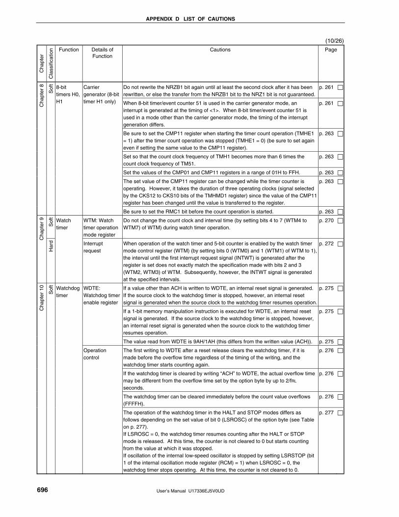
APPENDIX D LIST OF CAUTIONS
User’s Manual U17336EJ5V0UD 696
(10/26) C
hapt
er
Cla
ssifi
catio
n Function Details of Function
Cautions Page
Do not rewrite the NRZB1 bit again until at least the second clock after it has been rewritten, or else the transfer from the NRZB1 bit to the NRZ1 bit is not guaranteed.
p. 261
When 8-bit timer/event counter 51 is used in the carrier generator mode, an interrupt is generated at the timing of <1>. When 8-bit timer/event counter 51 is used in a mode other than the carrier generator mode, the timing of the interrupt generation differs.
p. 261
Be sure to set the CMP11 register when starting the timer count operation (TMHE1 = 1) after the timer count operation was stopped (TMHE1 = 0) (be sure to set again even if setting the same value to the CMP11 register).
p. 263
Set so that the count clock frequency of TMH1 becomes more than 6 times the count clock frequency of TM51.
p. 263
Set the values of the CMP01 and CMP11 registers in a range of 01H to FFH. p. 263
The set value of the CMP11 register can be changed while the timer counter is operating. However, it takes the duration of three operating clocks (signal selected by the CKS12 to CKS10 bits of the TMHMD1 register) since the value of the CMP11 register has been changed until the value is transferred to the register.
p. 263
Cha
pter
8
Sof
t
8-bit timers H0, H1
Carrier generator (8-bit timer H1 only)
Be sure to set the RMC1 bit before the count operation is started. p. 263
Sof
t
WTM: Watch timer operation mode register
Do not change the count clock and interval time (by setting bits 4 to 7 (WTM4 to WTM7) of WTM) during watch timer operation.
p. 270
Cha
pter
9
Har
d
Watch timer
Interrupt request
When operation of the watch timer and 5-bit counter is enabled by the watch timer mode control register (WTM) (by setting bits 0 (WTM0) and 1 (WTM1) of WTM to 1), the interval until the first interrupt request signal (INTWT) is generated after the register is set does not exactly match the specification made with bits 2 and 3 (WTM2, WTM3) of WTM. Subsequently, however, the INTWT signal is generated at the specified intervals.
p. 272
If a value other than ACH is written to WDTE, an internal reset signal is generated. If the source clock to the watchdog timer is stopped, however, an internal reset signal is generated when the source clock to the watchdog timer resumes operation.
p. 275
If a 1-bit memory manipulation instruction is executed for WDTE, an internal reset signal is generated. If the source clock to the watchdog timer is stopped, however, an internal reset signal is generated when the source clock to the watchdog timer resumes operation.
p. 275
WDTE: Watchdog timer enable register
The value read from WDTE is 9AH/1AH (this differs from the written value (ACH)). p. 275
The first writing to WDTE after a reset release clears the watchdog timer, if it is made before the overflow time regardless of the timing of the writing, and the watchdog timer starts counting again.
p. 276
If the watchdog timer is cleared by writing “ACH” to WDTE, the actual overflow time may be different from the overflow time set by the option byte by up to 2/fRL seconds.
p. 276
The watchdog timer can be cleared immediately before the count value overflows (FFFFH).
p. 276
Cha
pter
10
Sof
t
Watchdog timer
Operation control
The operation of the watchdog timer in the HALT and STOP modes differs as follows depending on the set value of bit 0 (LSROSC) of the option byte (see Table on p. 277). If LSROSC = 0, the watchdog timer resumes counting after the HALT or STOP mode is released. At this time, the counter is not cleared to 0 but starts counting from the value at which it was stopped. If oscillation of the internal low-speed oscillator is stopped by setting LSRSTOP (bit 1 of the internal oscillation mode register (RCM) = 1) when LSROSC = 0, the watchdog timer stops operating. At this time, the counter is not cleared to 0.
p. 277

APPENDIX D LIST OF CAUTIONS
User’s Manual U17336EJ5V0UD 697
(11/26)
Cha
pter
Cla
ssifi
catio
n Function Details of Function
Cautions Page
pp. The combination of WDCS2 = WDCS1 = WDCS0 = 0 and WINDOW1 = WINDOW0 = 0 is prohibited. 277, 278
pp.
Setting overflow time of watchdog timer, setting window open period of watchdog timer
The watchdog timer continues its operation during self programming and EEPROM emulation of the flash memory. During processing, the interrupt acknowledge time is delayed. Set the overflow time and window size taking this delay into consideration.
277, 278
Cha
pter
10
Sof
t
Watchdog timer
Setting window open period of watchdog timer
The first writing to WDTE after a reset release clears the watchdog timer, if it is made before the overflow time regardless of the timing of the writing, and the watchdog timer starts counting again.
p. 278
Cha
pter
11
Sof
t
Clock output controller (48-pin products only
CKS: clock output select register
Set CCS3 to CCS0 while the clock output operation is stopped (CLOE = 0). p. 282
ADCR: 10-bit A/D conversion register, ADCRH: 8-bit A/D conversion register
When data is read from ADCR and ADCRH, a wait cycle is generated. Do not read data from ADCR and ADCRH when the CPU is operating on the subsystem clock and the peripheral hardware clock is stopped. For details, see CHAPTER 34 CAUTIONS FOR WAIT.
p. 286
A/D conversion must be stopped before rewriting bits FR0 to FR2, LV1, and LV0 to values other than the identical data.
p. 288 ADM: A/D converter mode register If data is written to ADM, a wait cycle is generated. Do not write data to ADM
when the CPU is operating on the subsystem clock and the peripheral hardware clock is stopped. For details, see CHAPTER 34 CAUTIONS FOR WAIT.
p. 288
Set the conversion times with the following conditions. • 4.0 V ≤ AVREF ≤ 5.5 V: fAD = 0.6 to 3.6 MHz • 2.7 V ≤ AVREF < 4.0 V: fAD = 0.6 to 1.8 MHz • 2.3 V ≤ AVREF < 2.7 V: fAD = 0.6 to 1.48 MHz
p. 289
When rewriting FR2 to FR0, LV1, and LV0 to other than the same data, stop A/D conversion once (ADCS = 0) beforehand.
p. 289
Change LV1 and LV0 from the default value, when 2.3 V ≤ AVREF < 2.7 V. p. 289
A/D conversion timer selection
The above conversion time does not include clock frequency errors. Select conversion time, taking clock frequency errors into consideration.
p. 289
When writing to the A/D converter mode register (ADM), analog input channel specification register (ADS), and A/D port configuration register (ADPC), the contents of ADCR may become undefined. Read the conversion result following conversion completion before writing to ADM, ADS, and ADPC. Using timing other than the above may cause an incorrect conversion result to be read.
p. 290 ADCR: 10-bit A/D conversion register
If data is read from ADCR, a wait cycle is generated. Do not read data from ADCR when the CPU is operating on the subsystem clock and the peripheral hardware clock is stopped. For details, see CHAPTER 34 CAUTIONS FOR WAIT.
p. 290
When writing to the A/D converter mode register (ADM), analog input channel specification register (ADS), and A/D port configuration register (ADPC), the contents of ADCRH may become undefined. Read the conversion result following conversion completion before writing to ADM, ADS, and ADPC. Using timing other than the above may cause an incorrect conversion result to be read.
p. 291
Cha
pter
12
Sof
t
A/D converter
ADCRH: 8-bit A/D conversion register
If data is read from ADCRH, a wait cycle is generated. Do not read data from ADCRH when the CPU is operating on the subsystem clock and the peripheral hardware clock is stopped. For details, see CHAPTER 34 CAUTIONS FOR WAIT.
p. 291

APPENDIX D LIST OF CAUTIONS
User’s Manual U17336EJ5V0UD 698
(12/26) C
hapt
er
Cla
ssifi
catio
n Function Details of Function
Cautions Page
Be sure to clear bits 3 to 7 to “0”. p. 292
If data is written to ADS, a wait cycle is generated. Do not write data to ADS when the CPU is operating on the subsystem clock and the peripheral hardware clock is stopped. For details, see CHAPTER 34 CAUTIONS FOR WAIT.
p. 292
ADS: Analog input channel specification register
For the 38-pin products, setting ADS2, ADS1, ADS0 to 1, 1, 0 or 1, 1, 1 is prohibited.
p. 292
pp. ADS: Analog input channel specification register, ADPC: A/D port configuration register (ADPC)
Set a channel to be used for A/D conversion in the input mode by using port mode register 2 (PM2). 292, 293
If data is written to ADPC, a wait cycle is generated. Do not write data to ADPC when the CPU is operating on the subsystem clock and the peripheral hardware clock is stopped. For details, see CHAPTER 34 CAUTIONS FOR WAIT.
p. 293 ADPC: A/D port configuration register (ADPC)
For the 38-pin products, setting ADPC3, ADPC2, ADPC1, ADPC0 to 0, 1, 1, 1 or 1, 0, 0, 0 is prohibited.
p. 293
PM2: Port mode register 2
For the 38-pin products, be sure to set bits 6 and 7 of PM2 to “1”, and bits 6 and 7 of P2 to “0”.
p. 294
Basic operations of A/D converter
Make sure the period of <1> to <5> is 1 μs or more. p. 295
Make sure the period of <1> to <5> is 1 μs or more. p. 299
<1> may be done between <2> and <4>. p. 299
<1> can be omitted. However, ignore data of the first conversion after <5> in this case.
p. 299
A/D conversion operation
The period from <6> to <9> differs from the conversion time set using bits 5 to 1 (FR2 to FR0, LV1, LV0) of ADM. The period from <8> to <9> is the conversion time set using FR2 to FR0, LV1, and LV0.
p. 299
Sof
t
Operating current in STOP mode
The A/D converter stops operating in the STOP mode. At this time, the operating current can be reduced by clearing bit 7 (ADCS) and bit 0 (ADCE) of the A/D converter mode register (ADM) to 0. To restart from the standby status, clear bit 0 (ADIF) of interrupt request flag register 1L (IF1L) to 0 and start operation.
p. 302
Har
d Input range of ANI0 to ANI7
Observe the rated range of the ANI0 to ANI7 input voltage. If a voltage of AVREF or higher and AVSS or lower (even in the range of absolute maximum ratings) is input to an analog input channel, the converted value of that channel becomes undefined. In addition, the converted values of the other channels may also be affected.
p. 302
Conflict between A/D conversion result register (ADCR, ADCRH) write and ADCR or ADCRH read by instruction upon the end of conversion, ADCR or ADCRH read has priority. After the read operation, the new conversion result is written to ADCR or ADCRH.
p. 302
Cha
pter
12
Sof
t
A/D converter
Conflicting operations
Conflict between ADCR or ADCRH write and A/D converter mode register (ADM) write, analog input channel specification register (ADS), or A/D port configuration register (ADPC) write upon the end of conversion, ADM, ADS, or ADPC write has priority. ADCR or ADCRH write is not performed, nor is the conversion end interrupt signal (INTAD) generated.
p. 302

APPENDIX D LIST OF CAUTIONS
User’s Manual U17336EJ5V0UD 699
(13/26)
Cha
pter
Cla
ssifi
catio
n Function Details of Function
Cautions Page
Noise countermeasures
To maintain the 10-bit resolution, attention must be paid to noise input to the AVREF pin and ANI0 to ANI7 pins. <1> Connect a capacitor with a low equivalent resistance and a good frequency
response to the power supply. <2> The higher the output impedance of the analog input source, the greater the
influence. To reduce the noise, connecting external C as shown in Figure 12-20 is recommended.
<3> Do not switch these pins with other pins during conversion. <4> The accuracy is improved if the HALT mode is set immediately after the start
of conversion.
p. 302
The analog input pins (ANI0 to ANI7) are also used as input port pins (P20 to P27). When A/D conversion is performed with any of ANI0 to ANI7 selected, do not access P20 to P27 while conversion is in progress; otherwise the conversion resolution may be degraded. It is recommended to select pins used as P20 to P27 starting with the ANI0/P20 that is the furthest from AVREF.
p. 303 ANI0/P20 to ANI7/P27
If a digital pulse is applied to the pins adjacent to the pins currently used for A/D conversion, the expected value of the A/D conversion may not be obtained due to coupling noise. Therefore, do not apply a pulse to the pins adjacent to the pin undergoing A/D conversion.
p. 303
Input impedance of ANI0 to ANI7 pins
This A/D converter charges a sampling capacitor for sampling during sampling time. Therefore, only a leakage current flows when sampling is not in progress, and a current that charges the capacitor flows during sampling. Consequently, the input impedance fluctuates depending on whether sampling is in progress, and on the other states. To make sure that sampling is effective, however, it is recommended to keep the output impedance of the analog input source to within 10 kΩ, and to connect a capacitor of about 100 pF to the ANI0 to ANI7 pins (see Figure 12-20).
p. 303
Har
d
AVREF pin input impedance
A series resistor string of several tens of kΩ is connected between the AVREF and AVSS pins. Therefore, if the output impedance of the reference voltage source is high, this will result in a series connection to the series resistor string between the AVREF and AVSS pins, resulting in a large reference voltage error.
p. 303
Interrupt request flag (ADIF)
The interrupt request flag (ADIF) is not cleared even if the analog input channel specification register (ADS) is changed. Therefore, if an analog input pin is changed during A/D conversion, the A/D conversion result and ADIF for the pre-change analog input may be set just before the ADS rewrite. Caution is therefore required since, at this time, when ADIF is read immediately after the ADS rewrite, ADIF is set despite the fact A/D conversion for the post-change analog input has not ended. When A/D conversion is stopped and then resumed, clear ADIF before the A/D conversion operation is resumed.
p. 304
Conversion results just after A/D conversion start
The first A/D conversion value immediately after A/D conversion starts may not fall within the rating range if the ADCS bit is set to 1 within 1 μs after the ADCE bit was set to 1, or if the ADCS bit is set to 1 with the ADCE bit = 0. Take measures such as polling the A/D conversion end interrupt request (INTAD) and removing the first conversion result.
p. 304
Cha
pter
12
Sof
t
A/D converter
A/D conversion result register (ADCR, ADCRH) read operation
When a write operation is performed to the A/D converter mode register (ADM), analog input channel specification register (ADS), and A/D port configuration register (ADPC), the contents of ADCR and ADCRH may become undefined. Read the conversion result following conversion completion before writing to ADM, ADS, and ADPC. Using a timing other than the above may cause an incorrect conversion result to be read.
p. 304

APPENDIX D LIST OF CAUTIONS
User’s Manual U17336EJ5V0UD 700
(14/26) C
hapt
er
Cla
ssifi
catio
n Function Details of Function
Cautions Page
If clock supply to serial interface UART0 is not stopped (e.g., in the HALT mode), normal operation continues. If clock supply to serial interface UART0 is stopped (e.g., in the STOP mode), each register stops operating, and holds the value immediately before clock supply was stopped. The TXD0 pin also holds the value immediately before clock supply was stopped and outputs it. However, the operation is not guaranteed after clock supply is resumed. Therefore, reset the circuit so that POWER0 = 0, RXE0 = 0, and TXE0 = 0.
p. 306
Set POWER0 = 1 and then set TXE0 = 1 (transmission) or RXE0 = 1 (reception) to start communication.
p. 306
TXE0 and RXE0 are synchronized by the base clock (fXCLK0) set by BRGC0. To enable transmission or reception again, set TXE0 or RXE0 to 1 at least two clocks of base clock after TXE0 or RXE0 has been cleared to 0. If TXE0 or RXE0 is set within two clocks of base clock, the transmission circuit or reception circuit may not be initialized.
p. 306
pp.
UART mode
Set transmit data to TXS0 at least one base clock (fXCLK0) after setting TXE0 = 1.
306, 309
TXS0: Transmit shift register 0
Do not write the next transmit data to TXS0 before the transmission completion interrupt signal (INTST0) is generated.
p. 309
To start the transmission, set POWER0 to 1 and then set TXE0 to 1. To stop the transmission, clear TXE0 to 0, and then clear POWER0 to 0.
p. 311
To start the reception, set POWER0 to 1 and then set RXE0 to 1. To stop the reception, clear RXE0 to 0, and then clear POWER0 to 0.
p. 311
Set POWER0 to 1 and then set RXE0 to 1 while a high level is input to the RxD0 pin. If POWER0 is set to 1 and RXE0 is set to 1 while a low level is input, reception is started.
p. 311
TXE0 and RXE0 are synchronized by the base clock (fXCLK0) set by BRGC0. To enable transmission or reception again, set TXE0 or RXE0 to 1 at least two clocks of base clock after TXE0 or RXE0 has been cleared to 0. If TXE0 or RXE0 is set within two clocks of base clock, the transmission circuit or reception circuit may not be initialized.
p. 311
Set transmit data to TXS0 at least one base clock (fXCLK0) after setting TXE0 = 1. p. 311
Clear the TXE0 and RXE0 bits to 0 before rewriting the PS01, PS00, and CL0 bits. p. 311
Make sure that TXE0 = 0 when rewriting the SL0 bit. Reception is always performed with “number of stop bits = 1”, and therefore, is not affected by the set value of the SL0 bit.
p. 311
ASIM0: Asynchronous serial interface operation mode register 0
Be sure to set bit 0 to 1. p. 311
The operation of the PE0 bit differs depending on the set values of the PS01 and PS00 bits of asynchronous serial interface operation mode register 0 (ASIM0).
p. 312
For the stop bit of the receive data, only the first stop bit is checked regardless of the number of the stops bits.
p. 312
If an overrun error occurs, the next receive data is not written to receive buffer register 0 (RXB0) but discarded.
p. 312
ASIS0: Asynchronous serial interface reception error status register 0
If data is read from ASIS0, a wait cycle is generated. Do not read data from ASIS0 when the CPU is operating on the subsystem clock and the peripheral hardware clock is stopped. For details, see CHAPTER 34 CAUTIONS FOR WAIT.
p. 312
Sof
t
Make sure that bit 6 (TXE0) and bit 5 (RXE0) of the ASIM0 register = 0 when rewriting the MDL04 to MDL00 bits.
p. 314
Cha
pter
13
Har
d
Serial interface UART0
BRGC0: Baud rate generator control register 0 The baud rate value is the output clock of the 5-bit counter divided by 2. p. 314

APPENDIX D LIST OF CAUTIONS
User’s Manual U17336EJ5V0UD 701
(15/26)
Cha
pter
Cla
ssifi
catio
n Function Details of Function
Cautions Page
POWER0, TXE0, RXE0: Bits 7, 6, 5 of ASIM0
Clear POWER0 to 0 after clearing TXE0 and RXE0 to 0 to set the operation stop mode. To start the communication, set POWER0 to 1, and then set TXE0 or RXE0 to 1.
p. 315
UART mode Take relationship with the other party of communication when setting the port mode register and port register.
p. 316
UART transmission
After transmit data is written to TXS0, do not write the next transmit data before the transmission completion interrupt signal (INTST0) is generated.
p. 319
If a reception error occurs, read asynchronous serial interface reception error status register 0 (ASIS0) and then read receive buffer register 0 (RXB0) to clear the error flag. Otherwise, an overrun error will occur when the next data is received, and the reception error status will persist.
p. 320UART reception
Reception is always performed with the “number of stop bits = 1”. The second stop bit is ignored.
p. 320
Keep the baud rate error during transmission to within the permissible error range at the reception destination.
p. 323Error of baud rate
Make sure that the baud rate error during reception satisfies the range shown in (4) Permissible baud rate range during reception.
p. 323
Cha
pter
13
Sof
t
Serial interface UART0
Permissible baud rate range during reception
Make sure that the baud rate error during reception is within the permissible error range, by using the calculation expression shown below.
p. 325
The TXD6 output inversion function inverts only the transmission side and not the reception side. To use this function, the reception side must be ready for reception of inverted data.
p. 327
If clock supply to serial interface UART6 is not stopped (e.g., in the HALT mode), normal operation continues. If clock supply to serial interface UART6 is stopped (e.g., in the STOP mode), each register stops operating, and holds the value immediately before clock supply was stopped. The TXD6 pin also holds the value immediately before clock supply was stopped and outputs it. However, the operation is not guaranteed after clock supply is resumed. Therefore, reset the circuit so that POWER6 = 0, RXE6 = 0, and TXE6 = 0.
p. 327
Set POWER6 = 1 and then set TXE6 = 1 (transmission) or RXE6 = 1 (reception) to start communication.
p. 327
TXE6 and RXE6 are synchronized by the base clock (fXCLK6) set by CKSR6. To enable transmission or reception again, set TXE6 or RXE6 to 1 at least two clocks of the base clock after TXE6 or RXE6 has been cleared to 0. If TXE6 or RXE6 is set within two clocks of the base clock, the transmission circuit or reception circuit may not be initialized.
p. 327
Set transmit data to TXB6 at least one base clock (fXCLK6) after setting TXE6 = 1. p. 327
UART mode
If data is continuously transmitted, the communication timing from the stop bit to the next start bit is extended two operating clocks of the macro. However, this does not affect the result of communication because the reception side initializes the timing when it has detected a start bit. Do not use the continuous transmission function if the interface is used in LIN communication operation.
p. 327
Do not write data to TXB6 when bit 1 (TXBF6) of asynchronous serial interface transmission status register 6 (ASIF6) is 1.
p. 333
Do not refresh (write the same value to) TXB6 by software during a communication operation (when bits 7 and 6 (POWER6, TXE6) of asynchronous serial interface operation mode register 6 (ASIM6) are 1 or when bits 7 and 5 (POWER6, RXE6) of ASIM6 are 1).
p. 333
Cha
pter
14
Sof
t
Serial interface UART6
TXB6: Transmit buffer register 6
Set transmit data to TXB6 at least one base clock (fXCLK6) after setting TXE6 = 1. p. 333

APPENDIX D LIST OF CAUTIONS
User’s Manual U17336EJ5V0UD 702
(16/26) C
hapt
er
Cla
ssifi
catio
n Function Details of Function
Cautions Page
To start the transmission, set POWER6 to 1 and then set TXE6 to 1. To stop the transmission, clear TXE6 to 0, and then clear POWER6 to 0.
p. 335
To start the reception, set POWER6 to 1 and then set RXE6 to 1. To stop the reception, clear RXE6 to 0, and then clear POWER6 to 0.
p. 335
Set POWER6 to 1 and then set RXE6 to 1 while a high level is input to the RXD6 pin. If POWER6 is set to 1 and RXE6 is set to 1 while a low level is input, reception is started.
p. 335
TXE6 and RXE6 are synchronized by the base clock (fXCLK6) set by CKSR6. To enable transmission or reception again, set TXE6 or RXE6 to 1 at least two clocks of the base clock after TXE6 or RXE6 has been cleared to 0. If TXE6 or RXE6 is set within two clocks of the base clock, the transmission circuit or reception circuit may not be initialized.
p. 335
Set transmit data to TXB6 at least one base clock (fXCLK6) after setting TXE6 = 1. p. 335
Clear the TXE6 and RXE6 bits to 0 before rewriting the PS61, PS60, and CL6 bits. p. 335
Fix the PS61 and PS60 bits to 0 when used in LIN communication operation. p. 335
Clear TXE6 to 0 before rewriting the SL6 bit. Reception is always performed with “the number of stop bits = 1”, and therefore, is not affected by the set value of the SL6 bit.
p. 335
ASIM6: Asynchronous serial interface operation mode register 6
Make sure that RXE6 = 0 when rewriting the ISRM6 bit. p. 335
The operation of the PE6 bit differs depending on the set values of the PS61 and PS60 bits of asynchronous serial interface operation mode register 6 (ASIM6).
p. 336
For the stop bit of the receive data, only the first stop bit is checked regardless of the number of stop bits.
p. 336
If an overrun error occurs, the next receive data is not written to receive buffer register 6 (RXB6) but discarded.
p. 336
ASIS6: Asynchronous serial interface reception error status register 6
If data is read from ASIS6, a wait cycle is generated. Do not read data from ASIS6 when the CPU is operating on the subsystem clock and the peripheral hardware clock is stopped. For details, see CHAPTER 34 CAUTIONS FOR WAIT.
p. 336
To transmit data continuously, write the first transmit data (first byte) to the TXB6 register. Be sure to check that the TXBF6 flag is “0”. If so, write the next transmit data (second byte) to the TXB6 register. If data is written to the TXB6 register while the TXBF6 flag is “1”, the transmit data cannot be guaranteed.
p. 337ASIF6: Asynchronous serial interface transmission status register 6 To initialize the transmission unit upon completion of continuous transmission, be
sure to check that the TXSF6 flag is “0” after generation of the transmission completion interrupt, and then execute initialization. If initialization is executed while the TXSF6 flag is “1”, the transmit data cannot be guaranteed.
p. 337
CKSR6: Clock selection register 6
Make sure POWER6 = 0 when rewriting TPS63 to TPS60. p. 338
Sof
t
Make sure that bit 6 (TXE6) and bit 5 (RXE6) of the ASIM6 register = 0 when rewriting the MDL67 to MDL60 bits.
p. 339
Har
d
BRGC6: Baud rate generator control register 6 The baud rate is the output clock of the 8-bit counter divided by 2. p. 339
ASICL6 can be refreshed (the same value is written) by software during a communication operation (when bits 7 and 6 (POWER6, TXE6) of ASIM6 = 1 or bits 7 and 5 (POWER6, RXE6) of ASIM6 = 1). However, do not set both SBRT6 and SBTT6 to 1 by a refresh operation during SBF reception (SBRT6 = 1) or SBF transmission (until INTST6 occurs since SBTT6 has been set (1)), because it may re-trigger SBF reception or SBF transmission.
p. 340
Cha
pter
14
Sof
t
Serial interface UART6
ASICL6: Asynchronous serial interface control register 6
In the case of an SBF reception error, the mode returns to the SBF reception mode. The status of the SBRF6 flag is held (1).
p. 341

APPENDIX D LIST OF CAUTIONS
User’s Manual U17336EJ5V0UD 703
(17/26)
Cha
pter
Cla
ssifi
catio
n Function Details of Function Cautions Page
Before setting the SBRT6 bit, make sure that bit 7 (POWER6) and bit 5 (RXE6) of ASIM6 = 1. After setting the SBRT6 bit to 1, do not clear it to 0 before SBF reception is completed (before an interrupt request signal is generated).
p. 341
The read value of the SBRT6 bit is always 0. SBRT6 is automatically cleared to 0 after SBF reception has been correctly completed.
p. 341
Before setting the SBTT6 bit to 1, make sure that bit 7 (POWER6) and bit 6 (TXE6) of ASIM6 = 1. After setting the SBTT6 bit to 1, do not clear it to 0 before SBF transmission is completed (before an interrupt request signal is generated).
p. 341
The read value of the SBTT6 bit is always 0. SBTT6 is automatically cleared to 0 at the end of SBF transmission.
p. 341
Do not set the SBRT6 bit to 1 during reception, and do not set the SBTT6 bit to 1 during transmission.
p. 341
ASICL6: Asynchronous serial interface control register 6
Before rewriting the DIR6 and TXDLV6 bits, clear the TXE6 and RXE6 bits to 0. p. 341
POWER6, TXE6, RXE6: Bits 7, 6, 5 of ASIM6
Clear POWER6 to 0 after clearing TXE6 and RXE6 to 0 to stop the operation. To start the communication, set POWER6 to 1, and then set TXE6 or RXE6 to 1.
p. 343
UART mode Take the relationship with the other party of communication when setting the port mode register and port register.
p. 344
Parity types and operation
Fix the PS61 and PS60 bits to 0 when the device is used in LIN communication operation.
p. 347

APPENDIX D LIST OF CAUTIONS
User’s Manual U17336EJ5V0UD 704
(18/26) C
hapt
er
Cla
ssifi
catio
n Function Details of Function Cautions Page
Cha
pter
14
Sof
t
Serial interface UART6
Permissible baud rate range during reception
Make sure that the baud rate error during reception is within the permissible error range, by using the calculation expression shown below.
p. 361
SOTB10: Transmit buffer register 10
Do not access SOTB10 when CSOT10 = 1 (during serial communication). p. 366
SIO10: Serial I/O shift register 10
Do not access SIO10 when CSOT10 = 1 (during serial communication). p. 366
CSIM10: Serial operation mode register 10
Be sure to clear bit 5 to 0. p. 367
Do not write to CSIC10 while CSIE10 = 1 (operation enabled). p. 369
To use P10/SCK10/TXD0 and P12/SO10 as general-purpose ports, set CSIC10 in the default status (00H).
p. 369
CSIC10: Serial clock selection register 10
The phase type of the data clock is type 1 after reset. p. 369
3-wire serial I/O mode
Take the relationship with the other party of communication when setting the port mode register and port register.
p. 372
Communication operation
Do not access the control register and data register when CSOT10 = 1 (during serial communication).
p. 373
Cha
pter
15
Sof
t
Serial interface CSI10
SO10 output If a value is written to TRMD10, DAP10, and DIR10, the output value of SO10 changes.
p. 381
− Do not use serial interface IIC0 and the multiplier/divider simultaneously, because various flags corresponding to interrupt request sources are shared among serial interface IIC0 and the multiplier/divider.
p. 382
Do not write data to IIC0 during data transfer. p. 385IIC0: IIC shift register 0 Write or read IIC0 only during the wait period. Accessing IIC0 in a
communication state other than during the wait period is prohibited. When the device serves as the master, however, IIC0 can be written only once after the communication trigger bit (STT0) is set to 1.
p. 385
The start condition is detected immediately after I2C is enabled to operate (IICE0 = 1) while the SCL0 line is at high level and the SDA0 line is at low level. Immediately after enabling I2C to operate (IICE0 = 1), set LREL0 (1) by using a 1-bit memory manipulation instruction.
p. 389IICC0: IIC control register 0
When bit 3 (TRC0) of IIC status register 0 (IICS0) is set to 1, WREL0 is set to 1 during the ninth clock and wait is canceled, after which TRC0 is cleared and the SDA0 line is set to high impedance.
p. 392
IICS0: IIC status register 0
If data is read from IICS0, a wait cycle is generated. Do not read data from IICS0 when the CPU is operating on the subsystem clock and the peripheral hardware clock is stopped. For details, see CHAPTER 34 CAUTIONS FOR WAIT.
p. 393
Write to STCEN only when the operation is stopped (IICE0 = 0). p. 396
As the bus release status (IICBSY = 0) is recognized regardless of the actual bus status when STCEN = 1, when generating the first start condition (STT0 = 1), it is necessary to verify that no third party communications are in progress in order to prevent such communications from being destroyed.
p. 396
IICF0: IIC flag register 0
Write to IICRSV only when the operation is stopped (IICE0 = 0). p. 396
Cha
pter
16
Sof
t
Serial interface IIC0
Selection clock setting
Determine the transfer clock frequency of I2C by using CLX0, SMC0, CL01, and CL00 before enabling the operation (by setting bit 7 (IICE0) of IIC control register 0 (IICC0) to 1). To change the transfer clock frequency, clear IICE0 once to 0.
p. 399

APPENDIX D LIST OF CAUTIONS
User’s Manual U17336EJ5V0UD 705
(19/26)
Cha
pter
Cla
ssifi
catio
n Function Details of Function Cautions Page
When STCEN = 0
Immediately after I2C operation is enabled (IICE0 = 1), the bus communication status (IICBSY (bit 6 of IICF0) = 1) is recognized regardless of the actual bus status. When changing from a mode in which no stop condition has been detected to a master device communication mode, first generate a stop condition to release the bus, then perform master device communication. When using multiple masters, it is not possible to perform master device communication when the bus has not been released (when a stop condition has not been detected). Use the following sequence for generating a stop condition. <1> Set IIC clock selection register 0 (IICCL0). <2> Set bit 7 (IICE0) of IIC control register 0 (IICC0) to 1. <3> Set bit 0 (SPT0) of IICC0 to 1.
p. 416
When STCEN = 1
Immediately after I2C operation is enabled (IICE0 = 1), the bus released status (IICBSY = 0) is recognized regardless of the actual bus status. To generate the first start condition (STT0 (bit 1 of IIC control register 0 (IICC0)) = 1), it is necessary to confirm that the bus has been released, so as to not disturb other communications.
p. 416
If other I2C communications are already in progress
If I2C operation is enabled and the device participates in communication already in progress when the SDA0 pin is low and the SCL0 pin is high, the macro of I2C recognizes that the SDA0 pin has gone low (detects a start condition). If the value on the bus at this time can be recognized as an extension code, ACK is returned, but this interferes with other I2C communications. To avoid this, start I2C in the following sequence. <1> Clear bit 4 (SPIE0) of IICC0 to 0 to disable generation of an interrupt
request signal (INTIIC0) when the stop condition is detected. <2> Set bit 7 (IICE0) of IICC0 to 1 to enable the operation of I2C. <3> Wait for detection of the start condition. <4> Set bit 6 (LREL0) of IICC0 to 1 before ACK is returned (4 to 80 clocks
after setting IICE0 to 1), to forcibly disable detection.
p. 416
Transfer clock frequency setting
Determine the transfer clock frequency by using SMC0, CL01, CL00 (bits 3, 1, and 0 of IICL0), and CLX0 (bit 0 of IICX0) before enabling the operation (IICE0 = 1). To change the transfer clock frequency, clear IICE0 to 0 once.
p. 416
STT0, SPT0: Bits 1, 0 of IIC control register 0 (IICC0)
Setting STT0 and SPT0 (bits 1 and 0 of IICC0) again after they are set and before they are cleared to 0 is prohibited.
p. 417
Cha
pter
16
Sof
t
Serial interface IIC0
Transmission reserve When transmission is reserved, set SPIE0 (bit 4 of IICL0) to 1 so that an interrupt request is generated when the stop condition is detected. Transfer is started when communication data is written to IIC0 after the interrupt request is generated. Unless the interrupt is generated when the stop condition is detected, the device stops in the wait state because the interrupt request is not generated when communication is started. However, it is not necessary to set SPIE0 to 1 when MSTS0 (bit 7 of IICS0) is detected by software.
p. 417
− Do not use serial interface IIC0 and the multiplier/divider simultaneously, because various flags corresponding to interrupt request sources are shared among serial interface IIC0 and the multiplier/divider.
p. 453
The value read from SDR0 during operation processing (while bit 7 (DMUE) of multiplier/divider control register 0 (DMUC0) is 1) is not guaranteed.
p. 455SDR0: Remainder data register 0
SDR0 is reset when the operation is started (when DMUE is set to 1). p. 455
MDA0H is cleared to 0 when an operation is started in the multiplication mode (when multiplier/divider control register 0 (DMUC0) is set to 81H).
p. 455
Do not change the value of MDA0 during operation processing (while bit 7 (DMUE) of multiplier/divider control register 0 (DMUC0) is 1). Even in this case, the operation is executed, but the result is undefined.
p. 455
Cha
pter
17
Sof
t
Multiplier/ divider (μPD78F0514, 78F0515, and 78F0515D only)
MDA0H, MDA0L: Multiplication/ division data register A0
The value read from MDA0 during operation processing (while DMUE is 1) is not guaranteed.
p. 455

APPENDIX D LIST OF CAUTIONS
User’s Manual U17336EJ5V0UD 706
(20/26) C
hapt
er
Cla
ssifi
catio
n Function Details of Function
Cautions Page
Do not change the value of MDB0 during operation processing (while bit 7 (DMUE) of multiplier/divider control register 0 (DMUC0) is 1). Even in this case, the operation is executed, but the result is undefined.
p. 456MDB0: Multiplication/ division data register B0 Do not clear MDB0 to 0000H in the division mode. If set, undefined operation
results are stored in MDA0 and SDR0. p. 456
If DMUE is cleared to 0 during operation processing (when DMUE is 1), the operation result is not guaranteed. If the operation is completed while the clearing instruction is being executed, the operation result is guaranteed, provided that the interrupt flag is set.
p. 457
Do not change the value of DMUSEL0 during operation processing (while DMUE is 1). If it is changed, undefined operation results are stored in multiplication/division data register A0 (MDA0) and remainder data register 0 (SDR0).
p. 457
Cha
pter
17
Sof
t
Multiplier/ divider (μPD78F0514, 78F0515, and 78F0515D only)
DMUC0: Multiplier/divider control register 0
If DMUE is cleared to 0 during operation processing (while DMUE is 1), the operation processing is stopped. To execute the operation again, set multiplication/division data register A0 (MDA0), multiplication/division data register B0 (MDB0), and multiplier/divider control register 0 (DMUC0), and start the operation (by setting DMUE to 1).
p. 457
Be sure to clear bits 6 and 7 of IF1L to 0 in the 38-pin and 44-pin products. Be sure to clear bit 7 of IF1L to 0 in the 48-pin products.
p. 468
Be sure to clear bits 1 to 7 of IF1H to 0. p. 468
When operating a timer, serial interface, or A/D converter after standby release, operate it once after clearing the interrupt request flag. An interrupt request flag may be set by noise.
p. 468
1F0L, 1F0L, 1F1L, 1F1H: Interrupt request flag registers
When manipulating a flag of the interrupt request flag register, use a 1-bit memory manipulation instruction (CLR1). When describing in C language, use a bit manipulation instruction such as “IF0L.0 = 0;” or “_asm(“clr1 IF0L, 0”);” because the compiled assembler must be a 1-bit memory manipulation instruction (CLR1). If a program is described in C language using an 8-bit memory manipulation instruction such as “IF0L &= 0xfe;” and compiled, it becomes the assembler of three instructions. mov a, IF0L and a, #0FEH mov IF0L, a In this case, even if the request flag of another bit of the same interrupt request flag register (IF0L) is set to 1 at the timing between “mov a, IF0L” and “mov IF0L, a”, the flag is cleared to 0 at “mov IF0L, a”. Therefore, care must be exercised when using an 8-bit memory manipulation instruction in C language.
p. 469
Be sure to set bits 6 and 7 of MK1L to 1 in the 38-pin and 44-pin products. Be sure to set bit 7 of MK1L to 1 in the 48-pin products.
p. 470MK0L, MK0H, MK1L, MK1H: Interrupt mask flag registers
Be sure to set bits 1 to 7 of MK1H to 1. p. 470
Be sure to set bits 6 and 7 of PR1L to 1 in the 38-pin and 44-pin products. Be sure to set bit 7 of PR1L to 1 in the 48-pin products.
p. 471PR0L, PR0H, PR1L, PR1H: Priority specification flag registers
Be sure to set bits 1 to 7 of PR1H to 1. p. 471
Be sure to clear bits 6 and 7 of EGP and EGN to 0 in the 38-pin and 44-pin products. Be sure to clear bit 7 of EGP and EGN to 0 in the 48-pin products.
p. 472EGP, EGN: External interrupt rising edge, falling edge enable registers
Select the port mode by clearing EGPn and EGNn to 0 because an edge may be detected when the external interrupt function is switched to the port function.
p. 472
Cha
pter
18
Sof
t
Interrupt function
Software interrupt request
Do not use the RETI instruction for restoring from the software interrupt. p. 476

APPENDIX D LIST OF CAUTIONS
User’s Manual U17336EJ5V0UD 707
(21/26)
Cha
pter
Cla
ssifi
catio
n Function Details of Function
Cautions Page
Cha
pter
18
Sof
t
Interrupt function
BRK instruction The BRK instruction is not one of the above-listed interrupt request hold instructions. However, the software interrupt activated by executing the BRK instruction causes the IE flag to be cleared. Therefore, even if a maskable interrupt request is generated during execution of the BRK instruction, the interrupt request is not acknowledged.
p. 480
For the 38-pin products, be sure to set bits 2 and 3 of KRM, PM7, and P7 to “0”. p. 482
If any of the KRM0 to KRM3 bits used is set to 1, set bits 0 to 3 (PU70 to PU73) of the corresponding pull-up resistor register 7 (PU7) to 1.
p. 482
If KRM is changed, the interrupt request flag may be set. Therefore, disable interrupts and then change the KRM register. Clear the interrupt request flag and enable interrupts.
p. 482
Cha
pter
19
Sof
t
Key interrupt function
KRM: Key return mode register
The bits not used in the key interrupt mode can be used as normal ports. p. 482
The STOP mode can be used only when the CPU is operating on the main system clock. The subsystem clock oscillation cannot be stopped. The HALT mode can be used when the CPU is operating on either the main system clock or the subsystem clock.
p. 483
When shifting to the STOP mode, be sure to stop the peripheral hardware operation operating with main system clock before executing STOP instruction.
p. 483
Standby function
The following sequence is recommended for operating current reduction of the A/D converter when the standby function is used: First clear bit 7 (ADCS) and bit 0 (ADCE) of the A/D converter mode register (ADM) to 0 to stop the A/D conversion operation, and then execute the STOP instruction.
p. 483
After the above time has elapsed, the bits are set to 1 in order from MOST11 and remain 1.
p. 484
Sof
t
The oscillation stabilization time counter counts up to the oscillation stabilization time set by OSTS. If the STOP mode is entered and then released while the internal high-speed oscillation clock is being used as the CPU clock, set the oscillation stabilization time as follows. • Desired OSTC oscillation stabilization time ≤ Oscillation stabilization time set by
OSTS Note, therefore, that only the status up to the oscillation stabilization time set by OSTS is set to OSTC after STOP mode is released.
p. 484
Har
d
OSTC: Oscillation stabilization time counter status register
The X1 clock oscillation stabilization wait time does not include the time until clock oscillation starts (“a” below).
p. 484
To set the STOP mode when the X1 clock is used as the CPU clock, set OSTS before executing the STOP instruction.
p. 485
Do not change the value of the OSTS register during the X1 clock oscillation stabilization time.
p. 485
Sof
t
The oscillation stabilization time counter counts up to the oscillation stabilization time set by OSTS. If the STOP mode is entered and then released while the internal high-speed oscillation clock is being used as the CPU clock, set the oscillation stabilization time as follows. • Desired OSTC oscillation stabilization time ≤ Oscillation stabilization time set by
OSTS Note, therefore, that only the status up to the oscillation stabilization time set by OSTS is set to OSTC after STOP mode is released.
p. 485
Cha
pter
20
Har
d
Standby function
OSTS: Oscillation stabilization time select register
The X1 clock oscillation stabilization wait time does not include the time until clock oscillation starts (“a” below).
p. 485

APPENDIX D LIST OF CAUTIONS
User’s Manual U17336EJ5V0UD 708
(22/26) C
hapt
er
Cla
ssifi
catio
n Function Details of Function
Cautions Page
Because the interrupt request signal is used to clear the standby mode, if there is an interrupt source with the interrupt request flag set and the interrupt mask flag reset, the standby mode is immediately cleared if set. Thus, the STOP mode is reset to the HALT mode immediately after execution of the STOP instruction and the system returns to the operating mode as soon as the wait time set using the oscillation stabilization time select register (OSTS) has elapsed.
p. 491
To use the peripheral hardware that stops operation in the STOP mode, and the peripheral hardware for which the clock that stops oscillating in the STOP mode after the STOP mode is released, restart the peripheral hardware.
p. 493
Even if “internal low-speed oscillator can be stopped by software” is selected by the option byte, the internal low-speed oscillation clock continues in the STOP mode in the status before the STOP mode is set. To stop the internal low-speed oscillator’s oscillation in the STOP mode, stop it by software and then execute the STOP instruction.
p. 493
To shorten oscillation stabilization time after the STOP mode is released when the CPU operates with the high-speed system clock (X1 oscillation), temporarily switch the CPU clock to the internal high-speed oscillation clock before the next execution of the STOP instruction. Before changing the CPU clock from the internal high-speed oscillation clock to the high-speed system clock (X1 oscillation) after the STOP mode is released, check the oscillation stabilization time with the oscillation stabilization time counter status register (OSTC).
p. 493
Cha
pter
20
Sof
t
Standby function
STOP mode
If the STOP instruction is executed when AMPH = 1, supply of the CPU clock is stopped for 4.06 to 16.12 μs after the STOP mode is released when the internal high-speed oscillation clock is selected as the CPU clock, or for the duration of 160 external clocks when the high-speed system clock (external clock input) is selected as the CPU clock.
p. 493
For an external reset, input a low level for 10 μs or more to the RESET pin. p. 497
During reset input, the X1 clock, XT1 clock, internal high-speed oscillation clock, and internal low-speed oscillation clock stop oscillating. External main system clock input and external subsystem clock input become invalid.
p. 497
−
When the STOP mode is released by a reset, the STOP mode contents are held during reset input. However, the port pins become high-impedance, except for P130, which is set to low-level output.
p. 497
Block diagram of reset function
An LVI circuit internal reset does not reset the LVI circuit. p. 498
Har
d
Watchdog timer overflow
A watchdog timer internal reset resets the watchdog timer. p. 499
Cha
pter
21
Sof
t
Reset function
RESF: Reset control flag register
Do not read data by a 1-bit memory manipulation instruction. p. 505
If an internal reset signal is generated in the POC circuit, the reset control flag register (RESF) is cleared to 00H.
p. 506
pp.
−
Set the low-voltage detector by software after the reset status is released (see CHAPTER 23 LOW-VOLTAGE DETECTOR). 508, 509
In 2.7 V/1.59 V POC mode
A voltage oscillation stabilization time of 1.93 to 5.39 ms is required after the supply voltage reaches 1.59 V (TYP.). If the supply voltage rises from 1.59 V (TYP.) to 2.7 V (TYP.) within 1.93 ms, the power supply oscillation stabilization time of 0 to 5.39 ms is automatically generated before reset processing.
p. 509
Cha
pter
22
Sof
t
Power-on-clear circuit
Cautions for power-on-clear circuit
In a system where the supply voltage (VDD) fluctuates for a certain period in the vicinity of the POC detection voltage (VPOC), the system may be repeatedly reset and released from the reset status. In this case, the time from release of reset to the start of the operation of the microcontroller can be arbitrarily set by taking the following action.
p. 510

APPENDIX D LIST OF CAUTIONS
User’s Manual U17336EJ5V0UD 709
(23/26)
Cha
pter
Cla
ssifi
catio
n Function Details of Function
Cautions Page
Sof
t
To stop LVI, follow either of the procedures below. • When using 8-bit memory manipulation instruction: Write 00H to LVIM. • When using 1-bit memory manipulation instruction: Clear LVION to 0.
p. 514
Har
d Input voltage from external input pin (EXLVI) must be EXLVI < VDD.
p. 514
After an LVI reset has been generated, do not write values to LVIS and LVIM when LVION = 1.
p. 514
LVIM: Low-voltage detection register
When using LVI as an interrupt, if LVION is cleared (0) in a state below the LVI detection voltage, an INTLVI signal is generated and LVIIF becomes 1.
p. 514
Be sure to clear bits 4 to 7 to “0”. p. 515
Do not change the value of LVIS during LVI operation. p. 515
When an input voltage from the external input pin (EXLVI) is detected, the detection voltage (VEXLVI = 1.21 V (TYP.)) is fixed. Therefore, setting of LVIS is not necessary.
p. 515
LVIS: Low-voltage detection level selection register
After an LVI reset has been generated, do not write values to LVIS and LVIM when LVION = 1.
p. 515
<1> must always be executed. When LVIMK = 0, an interrupt may occur immediately after the processing in <4>.
p. 517 When detecting level of supply voltage (VDD) If supply voltage (VDD) ≥ detection voltage (VLVI) when LVIMD is set to 1, an internal
reset signal is not generated. p. 517
<1> must always be executed. When LVIMK = 0, an interrupt may occur immediately after the processing in <3>.
p. 520
Sof
t
If input voltage from external input pin (EXLVI) ≥ detection voltage (VEXLVI = 1.21 V (TYP.)) when LVIMD is set to 1, an internal reset signal is not generated.
p. 520
When detecting level of input voltage from external input pin (EXLVI)
Input voltage from external input pin (EXLVI) must be EXLVI < VDD. p. 520
Har
d
When detecting level of input voltage from external input pin (EXLVI)
Input voltage from external input pin (EXLVI) must be EXLVI < VDD. p. 525
Cha
pter
23
Sof
t
Low-voltage detector
Cautions for low-voltage detector
In a system where the supply voltage (VDD) fluctuates for a certain period in the vicinity of the LVI detection voltage (VLVI), the operation is as follows depending on how the low-voltage detector is used. (1) When used as reset
The system may be repeatedly reset and released from the reset status. In this case, the time from release of reset to the start of the operation of the microcontroller can be arbitrarily set by taking action (1) below.
(2) When used as interrupt Interrupt requests may be frequently generated. Take (b) of action (2) below.
p. 527
0082H, 0083H/ 1082H, 1083H
Be sure to set 00H to 0082H and 0083H (0082H/1082H and 0083H/1083H when the boot swap function is used).
p. 530
0080H/1080H Set a value that is the same as that of 0080H to 1080H because 0080H and 1080H are switched during the boot swap operation.
p. 530
0081H/1081H POCMODE can only be written by using a dedicated flash memory programmer. It cannot be set during self programming or boot swap operation during self programming (at this time, 1.59 V POC mode (default) is set). However, because the value of 1081H is copied to 0081H during the boot swap operation, it is recommended to set a value that is the same as that of 0081H to 1081H when the boot swap function is used.
p. 530
Cha
pter
24
Sof
t
Option byte
0084H/1084H Be sure to set 00H (disabling on-chip debug operation) to 0084H for products not equipped with the on-chip debug function (μPD78F0511, 78F0512, 78F0513, 78F0514 and 78F0515). Also set 00H to 1084H because 0084H and 1084H are switched during the boot swap operation.
p. 531
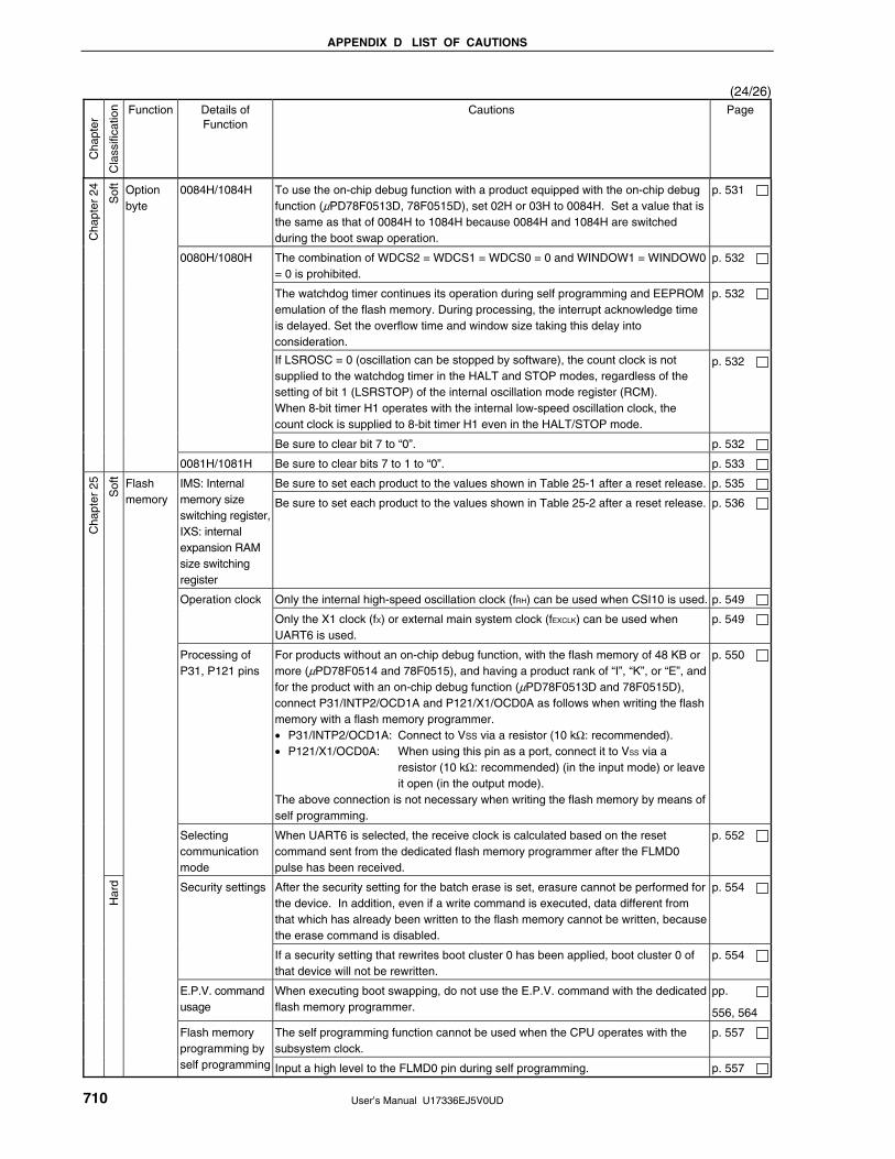
APPENDIX D LIST OF CAUTIONS
User’s Manual U17336EJ5V0UD 710
(24/26) C
hapt
er
Cla
ssifi
catio
n Function Details of Function
Cautions Page
0084H/1084H To use the on-chip debug function with a product equipped with the on-chip debug function (μPD78F0513D, 78F0515D), set 02H or 03H to 0084H. Set a value that is the same as that of 0084H to 1084H because 0084H and 1084H are switched during the boot swap operation.
p. 531
The combination of WDCS2 = WDCS1 = WDCS0 = 0 and WINDOW1 = WINDOW0 = 0 is prohibited.
p. 532
The watchdog timer continues its operation during self programming and EEPROM emulation of the flash memory. During processing, the interrupt acknowledge time is delayed. Set the overflow time and window size taking this delay into consideration.
p. 532
If LSROSC = 0 (oscillation can be stopped by software), the count clock is not supplied to the watchdog timer in the HALT and STOP modes, regardless of the setting of bit 1 (LSRSTOP) of the internal oscillation mode register (RCM). When 8-bit timer H1 operates with the internal low-speed oscillation clock, the count clock is supplied to 8-bit timer H1 even in the HALT/STOP mode.
p. 532
0080H/1080H
Be sure to clear bit 7 to “0”. p. 532
Cha
pter
24
Sof
t
Option byte
0081H/1081H Be sure to clear bits 7 to 1 to “0”. p. 533
Be sure to set each product to the values shown in Table 25-1 after a reset release. p. 535 IMS: Internal memory size switching register, IXS: internal expansion RAM size switching register
Be sure to set each product to the values shown in Table 25-2 after a reset release. p. 536
Only the internal high-speed oscillation clock (fRH) can be used when CSI10 is used. p. 549 Operation clock
Only the X1 clock (fX) or external main system clock (fEXCLK) can be used when UART6 is used.
p. 549
Processing of P31, P121 pins
For products without an on-chip debug function, with the flash memory of 48 KB or more (μPD78F0514 and 78F0515), and having a product rank of “I”, “K”, or “E”, and for the product with an on-chip debug function (μPD78F0513D and 78F0515D), connect P31/INTP2/OCD1A and P121/X1/OCD0A as follows when writing the flash memory with a flash memory programmer. • P31/INTP2/OCD1A: Connect to VSS via a resistor (10 kΩ: recommended). • P121/X1/OCD0A: When using this pin as a port, connect it to VSS via a
resistor (10 kΩ: recommended) (in the input mode) or leave it open (in the output mode).
The above connection is not necessary when writing the flash memory by means of self programming.
p. 550
Sof
t
Selecting communication mode
When UART6 is selected, the receive clock is calculated based on the reset command sent from the dedicated flash memory programmer after the FLMD0 pulse has been received.
p. 552
After the security setting for the batch erase is set, erasure cannot be performed for the device. In addition, even if a write command is executed, data different from that which has already been written to the flash memory cannot be written, because the erase command is disabled.
p. 554 Security settings
If a security setting that rewrites boot cluster 0 has been applied, boot cluster 0 of that device will not be rewritten.
p. 554
pp. E.P.V. command usage
When executing boot swapping, do not use the E.P.V. command with the dedicated flash memory programmer. 556, 564
The self programming function cannot be used when the CPU operates with the subsystem clock.
p. 557
Cha
pter
25
Har
d
Flash memory
Flash memory programming by self programming Input a high level to the FLMD0 pin during self programming. p. 557

APPENDIX D LIST OF CAUTIONS
User’s Manual U17336EJ5V0UD 711
(25/26)
Cha
pter
Cla
ssifi
catio
n Function Details of Function
Cautions Page
Be sure to execute the DI instruction before starting self programming. The self programming function checks the interrupt request flags (IF0L, IF0H, IF1L, and IF1H). If an interrupt request is generated, self programming is stopped.
p. 557
Self programming is also stopped by an interrupt request that is not masked even in the DI status. To prevent this, mask the interrupt by using the interrupt mask flag registers (MK0L, MK0H, MK1L, and MK1H).
p. 557
Cha
pter
25
Sof
t
Flash memory Flash memory programming by self programming
Allocate the entry program for self programming in the common area of 0000H to 7FFFH.
p. 557
μPD78F0513D, 78F0515D
The μPD78F0513D and 78F0515D have an on-chip debug function. Do not use these products for mass production because its reliability cannot be guaranteed after the on-chip debug function has been used, given the issue of the number of times the flash memory can be rewritten. NEC Electronics does not accept complaints concerning these products.
p. 566
Input the clock from the OCD0A/X1 pin during on-chip debugging. p. 566
Cha
pter
26
Har
d On-chip debug function (μPD78F0513D and 78F0515D only)
When OCD0A/X1 and OCD0B/X2 are used
Control the OCD0A/X1 and OCD0B/X2 pins by externally pulling down the OCD1A/P31 pin or by using an external circuit using the P130 pin (that outputs a low level when the device is reset).
p. 566
μPD78F0513D, 78F0515D
The μPD78F0513D and 78F0515D have an on-chip debug function. Do not use these products for mass production because its reliability cannot be guaranteed after the on-chip debug function has been used, given the issue of the number of times the flash memory can be rewritten. NEC Electronics does not accept complaints concerning these products.
p. 582
pp. Absolute maximum ratings
Product quality may suffer if the absolute maximum rating is exceeded even momentarily for any parameter. That is, the absolute maximum ratings are rated values at which the product is on the verge of suffering physical damage, and therefore the product must be used under conditions that ensure that the absolute maximum ratings are not exceeded.
582, 583, 603, 604, 622, 623, 641, 642
pp. When using the X1 oscillator, wire as follows in the area enclosed by the broken lines in the above figures to avoid an adverse effect from wiring capacitance. • Keep the wiring length as short as possible. • Do not cross the wiring with the other signal lines. • Do not route the wiring near a signal line through which a high fluctuating
current flows. • Always make the ground point of the oscillator capacitor the same potential as
VSS. • Do not ground the capacitor to a ground pattern through which a high current
flows.
• Do not fetch signals from the oscillator.
584, 605, 624, 643
pp.
Cha
pter
s 28
, 29,
30,
31
Har
d Electrical specifications
X1 oscillator characteristics
Since the CPU is started by the internal high-speed oscillation clock after a reset release, check the X1 clock oscillation stabilization time using the oscillation stabilization time counter status register (OSTC) by the user. Determine the oscillation stabilization time of the OSTC register and oscillation stabilization time select register (OSTS) after sufficiently evaluating the oscillation stabilization time with the resonator to be used.
584, 605, 624, 643

APPENDIX D LIST OF CAUTIONS
User’s Manual U17336EJ5V0UD 712
(26/26) C
hapt
er
Cla
ssifi
catio
n Function Details of Function
Cautions Page
pp. When using the XT1 oscillator, wire as follows in the area enclosed by the broken lines in the above figure to avoid an adverse effect from wiring capacitance • Keep the wiring length as short as possible. • Do not cross the wiring with the other signal lines. • Do not route the wiring near a signal line through which a high fluctuating
current flows. • Always make the ground point of the oscillator capacitor the same potential as
VSS. • Do not ground the capacitor to a ground pattern through which a high current
flows. • Do not fetch signals from the oscillator.
585, 606, 625, 644
pp.
XT1 oscillator characteristics
The XT1 oscillator is designed as a low-amplitude circuit for reducing power consumption, and is more prone to malfunction due to noise than the X1 oscillator. Particular care is therefore required with the wiring method when the XT1 clock is used.
585, 606, 625, 644
pp.
Cha
pter
s 28
, 29,
30,
31
Har
d Electrical specifications
Recommended oscillator constants
The oscillator constants shown above are reference values based on evaluation in a specific environment by the resonator manufacturer. If it is necessary to optimize the oscillator characteristics in the actual application, apply to the resonator manufacturer for evaluation on the implementation circuit. The oscillation voltage and oscillation frequency only indicate the oscillator characteristic. Use the 78K0/KC2 so that the internal operation conditions are within the specifications of the DC and AC characteristics.
586, 587
Cha
pter
33
Har
d Recommended soldering conditions
− Do not use different soldering methods together (except for partial heating). p. 665
Cha
pter
34
Sof
t
Wait − When the CPU is operating on the subsystem clock and the peripheral hardware clock is stopped, do not access the registers listed above using an access method in which a wait request is issued.
p. 667

User’s Manual U17336EJ5V0UD 713
APPENDIX E REVISION HISTORY
E.1 Major Revisions in This Edition (1/6)
Page Description Classification
Addition of (A2) grade products μPD78F0511GA(A2)-GAM-AX, 78F0511GB(A2)-GAF-AX, 78F0512GA(A2)-GAM-AX, 78F0512GB(A2)-GAF-AX, 78F0513GA(A2)-GAM-AX, 78F0513GB(A2)-GAF-AX, 78F0514GA(A2)-GAM-AX, 78F0515GA(A2)-GAM-AX
(A) grade products: Under development → Under mass production
Throughout
Addition of 38-pin products (under development) μPD78F0511MC-GAA-AX, 78F0512MC-GAA-AX, 78F0513MC-GAA-AX, 78F0513DMC-GAA-AX
(d)
CHAPTER 2 PIN FUNCTIONS
pp. 33 to 35 Addition of Note 1 to 2.1 Pin Function List (c)
p. 38 Addition of Caution 1 and Remark to 2.2.3 P20 to P27 (port 2) (c, d)
p. 39 Modification of Caution 2 and addition of description of QB-MINI2 to Remark 2 in 2.2.4 P30 to P33 (port 3)
(c, d)
p. 39 Addition of Caution to 2.2.5 P40 and P41 (port 4) (c, d)
p. 40 Addition of Caution and Remark to 2.2.7 P70 to P75 (port 7) (c, d)
p. 41 Modification of Caution and addition of description of QB-MINI2 to Remark 2 in 2.2.8 P120 to P124 (port 12)
(c, d)
p. 43 Addition of Note 2 to and modification of Note 3 in Table 2-2 Pin I/O Circuit Types (1/2) (c, d)
p. 44 Table 2-2 Pin I/O Circuit Types (2/2) • Modification of recommended connection of RESET pin • Addition of Note 1, modification of Note 4
(c, d)
CHAPTER 3 CPU ARCHITECTURE
p. 47 Addition of Note to Table 3-1 Set Values of Internal Memory Size Switching Register (IMS) and Internal Expansion RAM Size Switching Register (IXS)
(c)
p. 74 Addition of Note 2 to Table 3-7 Special Function Register List (4/4) (c)
CHAPTER 4 PORT FUNCTIONS
p. 87 Addition of Note 1 to Figure 4-1 Port Types (d)
p. 88 Addition of Note 1 to Table 4-2 Port Functions (1/2) (c, d)
p. 89 Addition of description on 38-pin products to Table 4-3 Port Configuration (d)
p. 97 Addition of Note and Caution 2 to 4.2.3 Port 2 (c, d)
p. 98 Addition of Note to Figure 4-9 Block Diagram of P20 to P27 (d)
p. 99 Modification of Caution 2 and addition of description on QB-MINI2 to Remark 2, in 4.2.4 Port 3 (c, d)
p. 102 Addition of Caution to 4.2.5 Port 4 (44-pin and 48-pin products only) (c)
p. 105 Addition of Note and Caution to 4.2.7 Port 7 (c, d)
p. 105 Addition of Note 1 to Figure 4-16 Block Diagram of P70 to P75 (d)
p. 106 Modification of Caution 2 and addition of description on QB-MINI2 to Remark 2, in 4.2.8 Port 12 (c, d)
p. 112 Modification of Caution in Figure 4-21 Format of Port Mode Register (c, d)
p. 113 Addition of Caution to Figure 4-22 Format of Port Register (c, d)
p. 115 Addition of Note to 4.3 (4) A/D port configuration register (ADPC) (d)
p. 115 Addition of Caution 3 to Figure 4-24 Format of A/D Port Configuration Register (ADPC) (c, d)
Remark “Classification” in the above table classifies revisions as follows.
(a): Error correction, (b): Addition/change of specifications, (c): Addition/change of description or note,
(d): Addition/change of package, part number, or management division, (e): Addition/change of related
documents

APPENDIX E REVISION HISTORY
User’s Manual U17336EJ5V0UD 714
(2/6)
Page Description Classification
p. 118 Addition of Note 1 to Table 4-5 Settings of Port Mode Register and Output Latch When Using Alternate Function
(d)
CHAPTER 5 CLOCK GENERATOR
p. 124 Modification of Cautions 2 and 3 (description regarding CPU clock supply stop period) in Figure 5-2 Format of Clock Operation Mode Select Register (OSCCTL)
(b)
p. 137 Addition of Notes 1 and 2 to Figure 5-12 Clock Generator Operation When Power Supply Voltage Is Turned On (When 1.59 V POC Mode Is Set (Option Byte: POCMODE = 0))
(c)
p. 140 Modification of Note in 5.6.1 (1) <1> Setting frequency (OSCCTL register) (b)
p. 148 Addition of Note to Figure 5-14 CPU Clock Status Transition Diagram (When 1.59 V POC Mode Is Set (Option Byte: POCMODE = 0))
(c, d)
p. 153 Modification of CPU clock supply stop periods after setting AMPH = 1, in Table 5-6 Changing CPU Clock
(b)
CHAPTER 6 16-BIT TIMER/EVENT COUNTER 00
Entire chapter
• TO00 pin output → TO00 output • Addition of TO00 output in block diagram
(a, c)
p. 167 Addition of explanation to Figure 6-8 Format of 16-bit Timer Output Control Register 00 (TOC00)
(c)
p. 169 Addition of Notes 1 and 2 to and modification of Note 3 in Figure 6-9 Format of Prescaler Mode Register 00 (PRM00)
(b, c)
p. 218 Addition of explanation to 6.5.1 Rewriting CR010 during TM00 operation (c)
CHAPTER 7 8-BIT TIMER/EVENT COUNTERS 50 AND 51
Entire chapter
• TO50 pin output → TO50 output, TO51 pin output → TO51 output • Addition of TO50, TO51 output in block diagram
(a, c)
p. 227 Addition of Notes 1 and 2 to Figure 7-5 Format of Timer Clock Selection Register 50 (TCL50) (b, c)
p. 228 Addition of Notes 1 and 2 to Figure 7-6 Format of Timer Clock Selection Register 51 (TCL51) (b, c)
p. 230 Addition of Caution 4 to Figure 7-7 Format of 8-bit Timer Mode Control Register 50 (TMC50) and Figure 7-8 Format of 8-bit Timer Mode Control Register 51 (TMC51)
(b, c)
CHAPTER 8 8-BIT TIMERS H0 AND H1
Entire chapter
• TOH0 pin output → TOH0 output, TOH1 pin output → TOH1 output • Addition of TOH0, TOH1 output in block diagram • Partial modification of description on PWM output
(a, c)
pp. 246, 247 Addition of Notes 1 and 2 and Caution 3 to Figure 8-5 Format of 8-bit Timer H Mode Register 0 (TMHMD0)
(b, c)
pp. 248, 249 Addition of Notes 1 and 2 and Caution 4 to Figure 8-6 Format of 8-bit Timer H Mode Register 1 (TMHMD1)
(b, c)
p. 261 Addition of Remark to Figure 8-13 Transfer Timing (c)
pp. 264, 265 Addition of Remark to Figure 8-15 Carrier Generator Mode Operation Timing (c)
CHAPTER 9 WATCH TIMER
p. 270 Addition of Note to Figure 9-2 Format of Watch Timer Operation Mode Register (WTM) (b, c)
CHAPTER 10 WATCHDOG TIMER
pp. 277, 278 Modification of Caution 5 in 10.4.1 Controlling operation of watchdog timer, Caution 2 in Table 10-3 Setting of Overflow Time of Watchdog Timer, and Caution 2 in Table 10-4 Setting Window Open Period of Watchdog Timer
(c)
Remark “Classification” in the above table classifies revisions as follows.
(a): Error correction, (b): Addition/change of specifications, (c): Addition/change of description or note,
(d): Addition/change of package, part number, or management division, (e): Addition/change of related
documents

APPENDIX E REVISION HISTORY
User’s Manual U17336EJ5V0UD 715
(3/6)
Page Description Classification
CHAPTER 11 CLOCK OUTPUT CONTROLLER (48-PIN PRODUCTS ONLY)
p. 282 Addition of Note 1 to Figure 11-2 Format of Clock Output Selection Register (CKS) (b, c)
CHAPTER 12 A/D CONVERTER
Entire chapter
Clarification of difference in number of A/D converter channels between 38-pin products and other products
(d)
p. 287 Modification of Figure 12-3 Format of A/D Converter Mode Register (ADM) (c)
p. 287 Modification of Table 12-1 Settings of ADCS and ADCE (c)
p. 288 Modification of Figure 12-4 Timing Chart When Comparator Is Used (c)
p. 292 Addition of Note and Caution 4 to Figure 12-8 Format of Analog Input Channel Specification Register (ADS)
(c, d)
p. 293 Addition of Caution 3 to Figure 12-9 Format of A/D Port Configuration Register (ADPC) (c, d)
p. 294 Addition of Caution to Figure 12-10 Format of Port Mode Register 2 (PM2) (c, d)
CHAPTER 13 SERIAL INTERFACE UART0
p. 308 Modification of Figure 13-1 Block Diagram of Serial Interface UART0 (c)
pp. 313, 314 Addition of Note 1 to and modification of Note 2 in Figure 13-4 Format of Baud Rate Generator Control Register 0 (BRGC0)
(b, c)
p. 323 Addition of Notes 1 and 2 to Table 13-4 Set Value of TPS01 and TPS00 (b, c)
CHAPTER 14 SERIAL INTERFACE UART6
p. 332 Modification of Figure 14-4 Block Diagram of Serial Interface UART6 (c)
p. 338 Addition of Notes 1 and 2 to and modification of Note 3 in Figure 14-8 Format of Clock Selection Register 6 (CKSR6)
(b, c)
p. 359 Addition of Notes 1 and 2 to Table 14-4 Set Value of TPS63 to TPS60 (b, c)
CHAPTER 15 SERIAL INTERFACE CSI10
pp. 368, 369 Addition of Notes 1 and 2 to Figure 15-3 Format of Serial Clock Selection Register 10 (CSIC10) (b, c)
CHAPTER 16 SERIAL INTERFACE IIC0
p. 382 Addition of Caution to 16.1 Functions of Serial Interface IIC0 (c)
p. 399 Addition of Notes 1 and 2 to Table 16-2 Selection Clock Setting (b)
CHAPTER 17 MULTIPLIER/DIVIDER (μPD78F0514, 78F0515, AND 78F0515D ONLY)
p. 453 Addition of Caution before 17.1 Functions of Multiplier/Divider (c)
p. 454 Modification of Figure 17-1 Block Diagram of Multiplier/Divider (a)
p. 458 Modification of description in 17.4.1 Multiplication operation (a)
p. 459 Modification of Figure 17-6 Timing Chart of Multiplication Operation (00DAH × 0093H) (a)
p. 460 Modification of description in 17.4.2 Division operation (a)
p. 461 Modification of Figure 17-7 Timing Chart of Division Operation (DCBA2586H ÷ 0018H) (a)
CHAPTER 18 INTERRUPT FUNCTIONS
Entire chapter
Clarification of difference in number of interrupt sources between 48-pin products and other products
(d)
p. 463 Modification of Note 4 in Table 18-1 Interrupt Source List (1/2) (c)
p. 467 Modification of Note 2 in and addition of Notes 3, 4, 6, and 8 to 10 to Table 18-2 Flags Corresponding to Interrupt Request Sources
(c)
p. 468 Modification of Caution 1 in Figure 18-2 Format of Interrupt Request Flag Registers (IF0L, IF0H, IF1L, IF1H)
(d)
Remark “Classification” in the above table classifies revisions as follows.
(a): Error correction, (b): Addition/change of specifications, (c): Addition/change of description or note,
(d): Addition/change of package, part number, or management division, (e): Addition/change of related
documents

APPENDIX E REVISION HISTORY
User’s Manual U17336EJ5V0UD 716
(4/6)
Page Description Classification
p. 470 Modification of Caution 1 in Figure 18-3 Format of Interrupt Mask Flag Registers (MK0L, MK0H, MK1L, MK1H)
(d)
p. 471 Modification of Caution 1 in Figure 18-4 Format of Priority Specification Flag Registers (PR0L, PR0H, PR1L, PR1H)
(d)
p. 472 Modification of Caution in Figure 18-5 Format of External Interrupt Rising Edge Enable Register (EGP) and External Interrupt Falling Edge Enable Register (EGN)
(d)
CHAPTER 19 KEY INTERRUPT FUNCTION
Entire chapter
Clarification of difference in number of key interrupt input pins between 38-pin products and other products
(d)
p. 482 Addition of Caution 1 to Figure 19-2 Format of Key Return Mode Register (KRM) (d)
CHAPTER 20 STANDBY FUNCTION
pp. 492, 493 Modification of description on serial interface IIC0 and Caution 4 (description regarding CPU clock supply stop period) in Table 20-3 Operating Statuses in STOP Mode
(b, c)
p. 493 Modification of Figure 20-5 Operation Timing When STOP Mode Is Released (When Unmasked Interrupt Request Is Generated)
(c)
pp. 494, 495 Modification of Figure 20-6 STOP Mode Release by Interrupt Request Generation (c)
CHAPTER 21 RESET FUNCTION
p. 502 Addition of Note 5 to Table 21-2 Hardware Statuses After Reset Acknowledgment (1/3) (c)
CHAPTER 22 POWER-ON-CLEAR CIRCUIT
p. 508 Modification of Notes 1 and 2 in and addition of Note 3 to Figure 22-2 Timing of Generation of Internal Reset Signal by Power-on-Clear Circuit and Low-Voltage Detector (1/2)
(d)
p. 509 Modification of Note 1 in Figure 22-2 Timing of Generation of Internal Reset Signal by Power-on-Clear Circuit and Low-Voltage Detector (2/2)
(d)
CHAPTER 23 LOW-VOLTAGE DETECTOR
p. 513 Modification of explanation in 23.3 (1) Low-voltage detection register (LVIM) (c)
p. 514 Addition of Notes 1 and 4 and Cautions 3 and 4 to Figure 23-2 Format of Low-Voltage Detection Register (LVIM)
(c)
p. 515 Modification of explanation in 23.3 (2) Low-voltage detection level selection register (LVIS) (c)
p. 515 Addition of Notes 1 and 2 and Caution 4 to Figure 23-3 Format of Low-Voltage Detection Level Selection Register (LVIS)
(c)
pp. 523, 524 Addition of Note 3 to Figure 23-7 Timing of Low-Voltage Detector Interrupt Signal Generation (Detects Level of Supply Voltage (VDD))
(c)
p. 526 Addition of Note 3 to Figure 23-8 Timing of Low-Voltage Detector Interrupt Signal Generation (Detects Level of Input Voltage from External Input Pin (EXLVI))
(c)
pp. 528, 529 Modification of Figure 23-9 Example of Software Processing After Reset Release (c)
CHAPTER 24 OPTION BYTE
p. 530 Modification of explanation in 24.1 (2) 0081H/1081H (d)
p. 532 Modification of Caution 2 in Figure 24-1 Format of Option Byte (1/2) (c)
CHAPTER 25 FLASH MEMORY
p. 536 Addition of Note to Table 25-1 Internal Memory Size Switching Register Settings and Table 25-2 Internal Expansion RAM Size Switching Register Settings
(c)
p. 537 Addition of (a) 38-pin products to Table 25-3 Wiring Between 78K0/KC2 and Dedicated Flash Memory Programmer
(d)
Remark “Classification” in the above table classifies revisions as follows.
(a): Error correction, (b): Addition/change of specifications, (c): Addition/change of description or note,
(d): Addition/change of package, part number, or management division, (e): Addition/change of related
documents
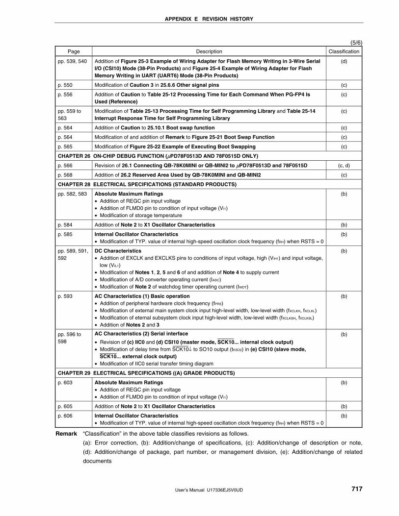
APPENDIX E REVISION HISTORY
User’s Manual U17336EJ5V0UD 717
(5/6)
Page Description Classification
pp. 539, 540 Addition of Figure 25-3 Example of Wiring Adapter for Flash Memory Writing in 3-Wire Serial I/O (CSI10) Mode (38-Pin Products) and Figure 25-4 Example of Wiring Adapter for Flash Memory Writing in UART (UART6) Mode (38-Pin Products)
(d)
p. 550 Modification of Caution 3 in 25.6.6 Other signal pins (c)
p. 556 Addition of Caution to Table 25-12 Processing Time for Each Command When PG-FP4 Is Used (Reference)
(c)
pp. 559 to 563
Modification of Table 25-13 Processing Time for Self Programming Library and Table 25-14 Interrupt Response Time for Self Programming Library
(c)
p. 564 Addition of Caution to 25.10.1 Boot swap function (c)
p. 564 Modification of and addition of Remark to Figure 25-21 Boot Swap Function (c)
p. 565 Modification of Figure 25-22 Example of Executing Boot Swapping (c)
CHAPTER 26 ON-CHIP DEBUG FUNCTION (μPD78F0513D AND 78F0515D ONLY)
p. 566 Revision of 26.1 Connecting QB-78K0MINI or QB-MINI2 to μPD78F0513D and 78F0515D (c, d)
p. 568 Addition of 26.2 Reserved Area Used by QB-78K0MINI and QB-MINI2 (c)
CHAPTER 28 ELECTRICAL SPECIFICATIONS (STANDARD PRODUCTS)
pp. 582, 583 Absolute Maximum Ratings • Addition of REGC pin input voltage • Addition of FLMD0 pin to condition of input voltage (VI1) • Modification of storage temperature
(b)
p. 584 Addition of Note 2 to X1 Oscillator Characteristics (b)
p. 585 Internal Oscillator Characteristics • Modification of TYP. value of internal high-speed oscillation clock frequency (fRH) when RSTS = 0
(b)
pp. 589, 591, 592
DC Characteristics • Addition of EXCLK and EXCLKS pins to conditions of input voltage, high (VIH1) and input voltage,
low (VIL1) • Modification of Notes 1, 2, 5 and 6 of and addition of Note 4 to supply current • Modification of A/D converter operating current (IADC) • Modification of Note 2 of watchdog timer operating current (IWDT)
(b)
p. 593 AC Characteristics (1) Basic operation • Addition of peripheral hardware clock frequency (fPRS) • Modification of external main system clock input high-level width, low-level width (fXCLKH, fXCLKL) • Modification of eternal subsystem clock input high-level width, low-level width (fXCLKSH, fXCLKSL) • Addition of Notes 2 and 3
(b)
pp. 596 to 598
AC Characteristics (2) Serial interface
• Revision of (c) IIC0 and (d) CSI10 (master mode, SCK10... internal clock output) • Modification of delay time from SCK10↓ to SO10 output (tKSO2) in (e) CSI10 (slave mode,
SCK10... external clock output) • Modification of IIC0 serial transfer timing diagram
(b)
CHAPTER 29 ELECTRICAL SPECIFICATIONS ((A) GRADE PRODUCTS)
p. 603 Absolute Maximum Ratings • Addition of REGC pin input voltage • Addition of FLMD0 pin to condition of input voltage (VI1)
(b)
p. 605 Addition of Note 2 to X1 Oscillator Characteristics (b)
p. 606 Internal Oscillator Characteristics • Modification of TYP. value of internal high-speed oscillation clock frequency (fRH) when RSTS = 0
(b)
Remark “Classification” in the above table classifies revisions as follows.
(a): Error correction, (b): Addition/change of specifications, (c): Addition/change of description or note,
(d): Addition/change of package, part number, or management division, (e): Addition/change of related
documents

APPENDIX E REVISION HISTORY
User’s Manual U17336EJ5V0UD 718
(6/6)
Page Description Classification
pp. 610, 611 DC Characteristics • Modification of MAX. value of supply current in operating mode (IDD1) and HALT mode (IDD2),
during subsystem clock oscillation • Modification of Notes 1, 2, 5 and 6 of and addition of Note 4 to supply current • Modification of A/D converter operating current (IADC) • Modification of Note 2 of watchdog timer operating current (IWDT)
(b)
p. 612 AC Characteristics (1) Basic operation • Addition of peripheral hardware clock frequency (fPRS) • Modification of external main system clock input high-level width, low-level width (fEXCLKH, fEXCLKL) • Modification of external subsystem clock input high-level width, low-level width (fEXCLKSH, fEXCLKSL) • Addition of Notes 2 and 3
(b)
pp. 615 to 617
AC Characteristics (2) Serial interface • Revision of (c) IIC0 and (d) CSI10 (master mode, SCK10... internal clock output) • Modification of delay time from SCK10↓ to SO10 output (tKSO2) in (e) CSI10 (slave mode,
SCK10... external clock output) • Modification of IIC0 serial transfer timing diagram
(b)
p. 621 Modification of number of rewrites per chip (Cerwr) in Flash Memory Programming Characteristics
(b)
CHAPTER 30 ELECTRICAL SPECIFICATIONS ((A2) GRADE PRODUCTS: TA = −40 to +110°C)
p. 622 Addition of chapter (b, d)
CHAPTER 31 ELECTRICAL SPECIFICATIONS ((A2) GRADE PRODUCTS: TA = −40 to +125°C)
p. 641 Addition of chapter (b, d)
CHAPTER 32 PACKAGE DRAWINGS
p. 660 Addition of package drawing of 38-pin plastic SSOP (7.62 mm (300)) (d)
CHAPTER 33 RECOMMENDED SOLDERING CONDITIONS
p. 665 Modification of Remark (d)
APPENDIX A DEVELOPMENT TOOLS
p. 669 Addition of Note 1 to and modification of Note 4 in Figure A-1 Development Tool Configuration (1/3)
(c, d)
p. 670 Addition of Note 1 to Figure A-1 Development Tool Configuration (2/3) (c)
p. 671 Addition of Figure A-1 Development Tool Configuration (3/3) (d)
p. 672 Modification of Note 1 in A.2 Language Processing Software (c)
p. 674 Addition of A.4.2 When using on-chip debug emulator with programming function QB-MINI2 (d)
p. 675 Addition of information on 38-pin products to and modification of Remark 1 in A.5.1 When using in-circuit emulator QB-78K0KX2
(d)
p. 676 Addition of A.5.3 When using on-chip debug emulator with programming function QB-MINI2 (d)
Remark “Classification” in the above table classifies revisions as follows.
(a): Error correction, (b): Addition/change of specifications, (c): Addition/change of description or note,
(d): Addition/change of package, part number, or management division, (e): Addition/change of related
documents
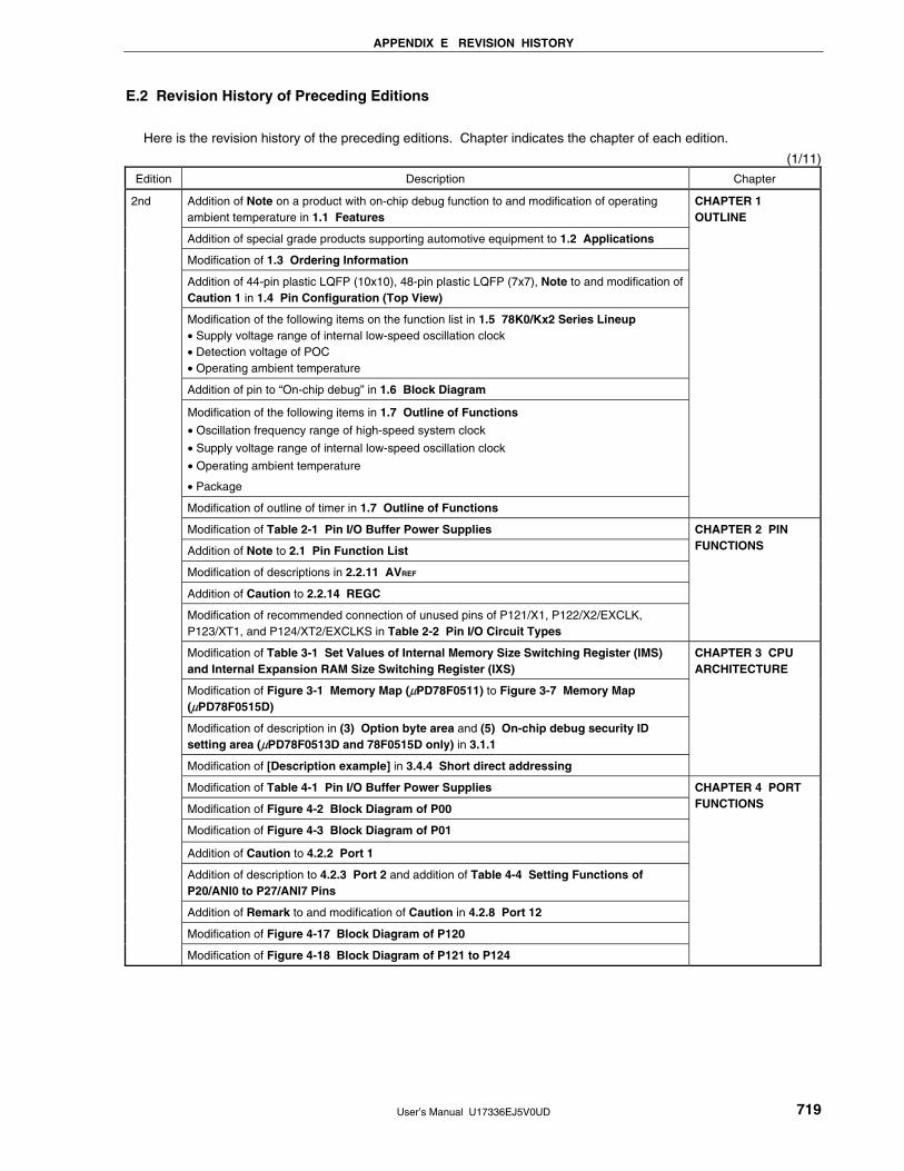
APPENDIX E REVISION HISTORY
User’s Manual U17336EJ5V0UD 719
E.2 Revision History of Preceding Editions
Here is the revision history of the preceding editions. Chapter indicates the chapter of each edition.
(1/11)
Edition Description Chapter
Addition of Note on a product with on-chip debug function to and modification of operating ambient temperature in 1.1 Features Addition of special grade products supporting automotive equipment to 1.2 Applications
Modification of 1.3 Ordering Information
Addition of 44-pin plastic LQFP (10x10), 48-pin plastic LQFP (7x7), Note to and modification of Caution 1 in 1.4 Pin Configuration (Top View)
Modification of the following items on the function list in 1.5 78K0/Kx2 Series Lineup • Supply voltage range of internal low-speed oscillation clock • Detection voltage of POC • Operating ambient temperature
Addition of pin to “On-chip debug” in 1.6 Block Diagram
Modification of the following items in 1.7 Outline of Functions
• Oscillation frequency range of high-speed system clock
• Supply voltage range of internal low-speed oscillation clock
• Operating ambient temperature
• Package
Modification of outline of timer in 1.7 Outline of Functions
CHAPTER 1 OUTLINE
Modification of Table 2-1 Pin I/O Buffer Power Supplies
Addition of Note to 2.1 Pin Function List
Modification of descriptions in 2.2.11 AVREF
Addition of Caution to 2.2.14 REGC
Modification of recommended connection of unused pins of P121/X1, P122/X2/EXCLK, P123/XT1, and P124/XT2/EXCLKS in Table 2-2 Pin I/O Circuit Types
CHAPTER 2 PIN FUNCTIONS
Modification of Table 3-1 Set Values of Internal Memory Size Switching Register (IMS) and Internal Expansion RAM Size Switching Register (IXS)
Modification of Figure 3-1 Memory Map (μPD78F0511) to Figure 3-7 Memory Map (μPD78F0515D)
Modification of description in (3) Option byte area and (5) On-chip debug security ID setting area (μPD78F0513D and 78F0515D only) in 3.1.1
Modification of [Description example] in 3.4.4 Short direct addressing
CHAPTER 3 CPU ARCHITECTURE
Modification of Table 4-1 Pin I/O Buffer Power Supplies
Modification of Figure 4-2 Block Diagram of P00
Modification of Figure 4-3 Block Diagram of P01
Addition of Caution to 4.2.2 Port 1
Addition of description to 4.2.3 Port 2 and addition of Table 4-4 Setting Functions of P20/ANI0 to P27/ANI7 Pins
Addition of Remark to and modification of Caution in 4.2.8 Port 12
Modification of Figure 4-17 Block Diagram of P120
2nd
Modification of Figure 4-18 Block Diagram of P121 to P124
CHAPTER 4 PORT FUNCTIONS

APPENDIX E REVISION HISTORY
User’s Manual U17336EJ5V0UD 720
(2/11)
Edition Description Chapter
Addition of a figure to Remark in 4.2.9 Port 13 (48-pin products only)
Addition of (4) A/D port configuration register (ADPC) to 4.3 Registers Controlling Port Function
Addition of Remark 2 and Notes 1 and 2 to Table 4-5 Settings of Port Mode Register and Output Latch When Using Alternate Function (2/2)
CHAPTER 4 PORT FUNCTIONS
Modification of oscillation frequency range X1 oscillator and external main system clock in 5.1 (1) Main system clock
Addition to description in 5.1 (3) Internal low-speed oscillation clock
Modification of Figure 5-1 Block Diagram of Clock Generator
Modification of Figure 5-3 Format of Processor Clock Control Register (PCC)
Addition of 5.3 (3) Setting of operation mode for subsystem clock pin
Modification of description in 5.3 (8) Oscillation stabilization time select register (OSTS)
Modification of oscillation frequency range in 5.4.1 X1 oscillator
Modification of description in 5.4.3 When subsystem clock is not used
Addition of Figure 5-12 Clock Generator Operation When Power Supply Voltage Is Turned On (When 1.59 V POC Mode Is Set (Option Byte: POCMODE = 0))
Addition of Figure 5-13 Clock Generator Operation When Power Supply Voltage Is Turned On (When 2.7 V/1.59 V POC Mode Is Set (Option Byte: POCMODE = 1))
Modification of 5.6.1 Controlling high-speed system clock
Modification of 5.6.2 Example of controlling internal high-speed oscillation clock
Modification of 5.6.3 Example of controlling subsystem clock
Modification of description in Table 5-4 Clocks Supplied to CPU and Peripheral Hardware, and Register Setting
Addition of Remark to Figure 5-14 CPU Clock Status Transition Diagram (When 1.59 V POC Mode Is Set (Option Byte: POCMODE = 0))
Modification of the following items in Table 5-5 CPU Clock Transition and SFR Register Setting Examples (3) CPU operating with subsystem clock (D) after reset release (A) (4) CPU clock changing from internal high-speed oscillation clock (B) to high-speed
system clock (C) (5) CPU clock changing from internal high-speed oscillation clock (B) to subsystem
clock (D) (7) CPU clock changing from high-speed system clock (C) to subsystem clock (D)
(9) CPU clock changing from subsystem clock (D) to high-speed system clock (C)
Modification of Table 5-6 Changing CPU Clock
Addition of 5.6.8 Time required for switchover of CPU clock and main system clock
Addition of 5.6.9 Conditions before clock oscillation is stopped
Addition of 5.6.10 Peripheral Hardware and Source Clocks
CHAPTER 5 CLOCK GENERATOR
Revision of chapter CHAPTER 6 16-BIT TIMER/EVENT COUNTERS 00
2nd
Modification of description in 7.2 (2) 8-bit timer compare register 5n (CR5n) CHAPTER 7 8-BIT TIMER/EVENT COUNTERS 50 AND 51

APPENDIX E REVISION HISTORY
User’s Manual U17336EJ5V0UD 721
(3/11)
Edition Description Chapter
Modification of Figure 8-2 Block Diagram of 8-bit Timer H1
Modification of description in (1) 8-bit timer H compare register 0n (CMP0n) and (2) 8-bit time r H compare register 1n (CMP1n) in 8.2
Modification of Figure 8-6 Format of 8-bit Timer H Mode Register 1 (TMHMD1)
Modification of Figure 8-12 (e) Operation by changing CMP1n (CMP1n = 02H → 03H, CMP0n = A5H)
Modification of description in 8.4.3 Carrier generator operation (8-bit timer H1 only)
Addition of <3> to Figure 8-13 Transfer Timing
Addition of <8> to Setting in 8.4.3
Modification of (a) Operation when CMP01 = N, CMP11 = N and (b) Operation when CMP01 = N, CMP11 = M in Figure 8-15
Modification of description in Figure 8-15 (c) Operation when CMP11 is changed
CHAPTER 8 8-BIT TIMERS H0 AND H1
Modification of description in 10.1 Functions of Watchdog Timer
Addition to description in and addition of Caution 4 to 10.4.1 Controlling operation of watchdog timer
CHAPTER 10 WATCHDOG TIMER
Addition of Note 1 and Cautions 1 and 2 to Figure 11-2 Format of Clock Output Selection Register (CKS)
CHAPTER 11 CLOCK OUTPUT CONTROLLER (48-PIN PRODUCTS ONLY)
Modification of the following items in 12.2 Configuration of A/D Converter (2) Sample & hold circuit (3) Series resistor string (5) Successive approximation register (SAR) (9) AVREF pin
Addition to Caution 1 in and addition of Caution 4 to Table 12-2 A/D Conversion Time Selection
Modification of Cautions 2 and 3 in Figure 12-8 Format of Analog Input Channel Specification Register (ADS)
Modification of description in 12.3 (5) A/D port configuration register (ADPC)
Modification of Cautions 1 and 2 in Figure 12-9 Format of A/D Port Configuration Register (ADPC)
Modification of Table 12-3 Setting Functions of ANI0/P20 to ANI7/P27 Pins
Modification of 12.4.1 Basic operations of A/D converter
Modification of description in Figure 12-11 Basic Operation of A/D Converter
Modification of expression in 12.4.2 Input voltage and conversion results
Modification of description in 12.4.3 A/D converter operation mode
2nd
Modification of the description of the following items in 12.6 Cautions for A/D Converter
(1) Operating current in STOP mode
(4) Noise countermeasures
(6) Input impedance of ANI0 to ANI7 pins
(11) Internal equivalent circuit
CHAPTER 12 A/D CONVERTER

APPENDIX E REVISION HISTORY
User’s Manual U17336EJ5V0UD 722
(4/11)
Edition Description Chapter
Addition of maximum transfer rate and Caution 4 to 13.1 (2) Asynchronous serial interface
(UART) mode
Addition of Caution 1 to 13.2 (3) Transmit shift register 0 (TXS0)
Addition of Caution 5 to Figure 13-2 Format of Asynchronous Serial Interface Operation
Mode Register 0 (ASIM0)
Modification of description in 13.3 (2) Asynchronous serial interface reception error status
register 0 (ASIS0)
Modification of Caution 1 in Figure 13-9 Reception Completion Interrupt Request Timing
Addition of Table 13-4 Set Value of TPS01 and TPS00
CHAPTER 13
SERIAL INTERFACE
UART0
Addition of maximum transfer rate and Cautions 4 and 5 to 14.1 (2) Asynchronous serial
interface (UART) mode
Modification of Figure 14-1 LIN Transmission Operation
Modification of Figure 14-2 LIN Reception Operation
Addition of Caution 3 to 14.2 (3) Transmit buffer register 6 (TXB6)
Addition of Cautions 4 and 5 to Figure 14-5 Format of Asynchronous Serial Interface
Operation Mode Register 6 (ASIM6)
Modification of description in 14.3 (2) Asynchronous serial interface reception error status
register 6 (ASIS6)
Addition of Caution 6 to Figure 14-10 Format of Asynchronous Serial Interface Control
Register 6 (ASICL6)
Modification of description in 14.3 (7) Input switch control register (ISC)
Modification of Caution 1 in 14.4.2 (2) (e) Normal reception
CHAPTER 14
SERIAL INTERFACE
UART6
Modification of Figure 15-1 Block Diagram of Serial Interface CSI10
Modification of Note 2 in Figure 15-2 Format of Serial Operation Mode Register 10
(CSIM10)
Modification of Caution 2 in Figure 15-3 Format of Serial Clock Selection Register 10
(CSIC10)
Modification of Note 1 of CSIM10 and CSIM11 in 15.4.1 (1) Register used
Addition of (b) Type 3: CKP10 = 1, DAP10 = 0 and (d) Type 4: CKP1n = 1, DAP1n = 1 to Figure 15-7 Output Operation of First Bit
Addition of (b) Type 3: CKP10 = 1, DAP10 = 0 and (d) Type 4: CKP10 = 1, DAP10 = 1 in Figure 15-8 Output Value of SO10 Pin (Last Bit)
Modification of Figure 16-1 Block Diagram of Serial Interface IIC0
Addition of Caution 2 to 16.2 (1) IIC shift register 0 (IIC0) and addition to description in (2) Slave address register 0 (SVA0)
Addition of 16.2 (13) Stop condition generator
2nd
Addition of description to IICE0 and addition of Caution to Figure 16-5 Format of IIC Control Register 0 (IICC0) (1/4)
CHAPTER 15
SERIAL INTERFACE
CSI10

APPENDIX E REVISION HISTORY
User’s Manual U17336EJ5V0UD 723
(5/11)
Edition Description Chapter
Addition of Note 2 to Figure 16-5 Format of IIC Control Register 0 (IICC0) (2/4)
Addition of description to STT0 in Figure 16-5 Format of IIC Control Register 0 (IICC0) (3/4)
Addition of clearing condition to STCF and IICBSY in Figure 16-7 Format of IIC Flag Register 0 (IICF0)
Modification of description in 16.3 (4) IIC clock selection register 0 (IICCL0)
Modification of description in 16.3 (6) I2C transfer clock setting method
Modification of Table 16-2 Selection Clock Setting
Addition of cause that ACK is not returned to 16.5.4 Acknowledge (ACK)
Addition of 16.5.7 Canceling wait
Modification of Table 16-6 Wait Periods and Figure 16-20 Communication Reservation Timing
Modification of Table 16-7 Wait Periods
Addition of (4) to (6) to 16.5.15 Cautions
Modification of 16.5.16 (1) Master operation (single-master system) and (2) Master operation (multi-master system)
Modification of Figure 16-25 Slave Operation Flowchart (1) and Figure 16-26 Slave Operation Flowchart (2)
Addition of Note to (a) (i) When WTIM0 = 0 to and modification of (ii) When WTIM0 = 1 in 16.5.17 (1) Master device operation
Addition of Notes 1 to 3 to (b) (i) When WTIM0 = 0 in 16.5.17 (1) Master device operation
Addition of Note to (c) (i) When WTIM0 = 0 in 16.5.17 (1) Master device operation
Modification of the value of the following items of IICS0 register in 16.5.17 (2) (d) (i) When WTIM0 = 0 (after restart, does not match with address
(= not extension code)) (2) (d) (ii) When WTIM0 = 1 (after restart, does not match with address
(= not extension code)) (3) (d) (i) When WTIM0 = 0 (after restart, does not match with address
(= not extension code)) (3) (d) (ii) When WTIM0 = 1 (after restart, does not match with address
(= not extension code)) (6) (d) (ii) Extension code (6) (e) When loss occurs due to stop condition during data transfer (6) (h) (ii) When WTIM0 = 1
Addition of description to 16.5.17 (5) Arbitration loss operation (operation as slave after arbitration loss) and (6) Operation when arbitration loss occurs (no communication after arbitration loss)
Addition of description when (i) When WTIM0 = 0 to the following items in 16.5.17 (6) Operation when arbitration loss occurs (no communication after arbitration loss) (f) When arbitration loss occurs due to low-level data when attempting to generate a
restart condition (g) When arbitration loss occurs due to a stop condition when attempting to generate a
restart condition
(h) When arbitration loss occurs due to low-level data when attempting to generate a stop condition
2nd
Modification of Figure 16-27 Example of Master to Slave Communication (When 9-Clock Wait Is Selected for Both Master and Slave) and Figure 16-28 Example of Slave to Master Communication (When 8-Clock Wait Is Selected for Master, 9-Clock Wait Is Selected for Slave)
CHAPTER 16 SERIAL INTERFACE IIC0

APPENDIX E REVISION HISTORY
User’s Manual U17336EJ5V0UD 724
(6/11)
Edition Description Chapter
Modification of Figure 17-7. Timing Chart of Division Operation (DCBA2586H ÷ 0018H) CHAPTER 17 MULTIPLIER/DIVIDER (μPD78F0514, 78F0515, AND 78F0515D ONLY)
Modification of Caution 3 in 20.1.1 Standby function
Modification of description in 20.1.2 (2) Oscillation stabilization time select register (OSTS)
Addition of clock output and buzzer output to items in and addition of Note to Table 20-1 Operating Statuses in HALT Mode
Modification of Figure 20-4 HALT Mode Release by Reset
Addition of clock output and buzzer output to items in Table 20-3 Operating Statuses in STOP Mode
Modification of Figure 20-5 Operation Timing When STOP Mode Is Released
Modification of Figure 20-7 STOP Mode Release by Reset
CHAPTER 20 STANDBY FUNCTION
Modification of Figure 21-2 Timing of Reset by RESET Input
Modification of Figure 21-3 Timing of Reset Due to Watchdog Timer Overflow
Modification of Figure 21-4 Timing of Reset in STOP Mode by RESET Input
Addition of clock output and buzzer output to items in Table 21-1 Operation Statuses During Reset Period
Modification of table in Note of Table 21-2 Hardware Statuses After Reset Acknowledgment (3/3)
CHAPTER 21 RESET FUNCTION
Addition of description of 2.7 V/1.59 V POC mode to 22.1 Functions of Power-on-Clear Circuit
Modification of 22.3 Operation of Power-on-Clear Circuit
Modification of Figure 22-3 Example of Software Processing After Reset Release (1/2)
CHAPTER 22 POWER-ON-CLEAR CIRCUIT
Modification of Figure 23-1 Block Diagram of Low-Voltage Detector
Modification of Figure 23-3 Format of Low-Voltage Detection Level Selection Register (LVIS)
Addition of (2) In 2.7 V/1.59 V POC mode (option byte: POCMODE = 1) to Figure 23-5 Timing of Low-Voltage Detector Internal Reset Signal Generation (Detects Level of Supply Voltage (VDD))
Modification of (1) In 1.59 V POC mode (option byte: POCMODE = 0) in and addition of (2) In 2.7 V/1.59 V POC mode (option byte: POCMODE = 1) to Figure 23-7 Timing of Low-Voltage Detector Interrupt Signal Generation (Detects Level of Supply Voltage (VDD))
Modification of Figure 23-8 Timing of Low-Voltage Detector Interrupt Signal Generation (Detects Level of Input Voltage from External Input Pin (EXLVI))
Modification of Figure 23-9 Example of Software Processing After Reset Release (1/2)
CHAPTER 23 LOW-VOLTAGE DETECTOR
Modification of description in 24.1 Functions of Option Bytes
Modification of Note in and addition of setting of area 0081H/1081H to 0084H/1084H to Figure 24-1 Format of Option Byte
2nd
Modification of description example of software for setting the option bytes
CHAPTER 24 OPTION BYTE

APPENDIX E REVISION HISTORY
User’s Manual U17336EJ5V0UD 725
(7/11)
Edition Description Chapter
Addition of Caution to Figure 25-1 Format of Internal Memory Size Switching Register (IMS)
Addition of Caution to Figure 25-2 Format of Internal Expansion RAM Size Switching Register (IXS)
Modification of value of VDD in Figure 25-3 Example of Wiring Adapter for Flash Memory Writing in 3-Wire Serial I/O (CSI10) Mode (44-pin products)
Modification of value of VDD in Figure 25-4 Example of Wiring Adapter for Flash Memory Writing in UART (UART6) Mode (44-pin products)
Modification of value of VDD in Figure 25-5 Example of Wiring Adapter for Flash Memory Writing in 3-Wire Serial I/O (CSI10) Mode (48-pin products)
Modification of value of VDD in Figure 25-6 Example of Wiring Adapter for Flash Memory Writing in UART (UART6) Mode (48-pin products)
Modification of transfer rate in (1) CSI10 and (2) UART6 in 25.5
Modification of transfer rate in Speed column of Table 25-7 Communication Modes
Addition of 25.8 Security Settings
Modification of 25.9.1 Boot swap function
CHAPTER 25 FLASH MEMORY
Revision of chapter CHAPTER 26 ON-CHIP DEBUG FUNCTION (μPD78F0513D AND 78F0515D ONLY)
Revision of chapter CHAPTER 28 ELECTRICAL SPECIFICATIONS (TARGET)
Addition of package drawing CHAPTER 29 PACKAGE DRAWINGS
Modification of <Conditions for maximum/minimum number of wait clocks> of A/D converter in Table 30-1 Registers That Generate Wait and Number of CPU Wait Clocks
CHAPTER 30 CAUTIONS FOR WAIT
Addition of (2) When using the on-chip debug emulator QB-78K0MINI to Figure A-1 Development Tool Configuration
Addition of A.5.2 When using on-chip debug emulator QB-78K0MINI
APPENDIX A DEVELOPMENT TOOLS
Addition of chapter APPENDIX B NOTES ON TARGET SYSTEM DESIGN
2nd
Addition of chapter APPENDIX D REVISION HISTORY
Extending value range of capacitor (“0.47 μF: target” → “0.47 to 1 μF: recommended”) Throughout
Addition of following related documents of device • 78K0/Kx2 Flash Memory Programming (Programmer) Application Note • 78K0/Kx2 Flash Memory Self Programming User’s Manual • PG-FPL3 Flash Memory Programmer User’s Manual
INTRODUCTION
Deletion of description concerning production process division management from 1.1 Features
Change of 1.3 Ordering Information
Deletion of description concerning production process division management from 1.5 78K0/Kx2 Series Lineup
3rd
Deletion of description concerning production process division management from 1.7 Outline of Functions
CHAPTER 1 OUTLINE

APPENDIX E REVISION HISTORY
User’s Manual U17336EJ5V0UD 726
(8/11)
Edition Description Chapter
Addition of Caution 2, Note, and Remark 1 to 2.2.4 P30 to P33 (port 3)
Addition of Caution, Note, and Remark 1 to 2.2.8 P120 to P124 (port 12)
Addition of following contents to Table 2-2 Pin I/O Circuit Types • Addition of Notes 2 and 3 and Remark to P31/INTP2/OCD1A pin • Addition of Notes 2 and 5 and Remark to P121/X1/OCD0A pin • Addition of Note 4 to FLMD0 pin • Addition of connection of RESET pin when not used
CHAPTER 2 PIN FUNCTIONS
Addition of Remark and block number figure to Figures 3-1 Memory Map (μPD78F0511) to 3-7 Memory Map (μPD78F0515D)
Addition of Table 3-2 Correspondence Between Address Values and Block Numbers of Flash Memory
CHAPTER 3 CPU ARCHITECTURE
Change of setting of digital input and output in Table 4-4 Setting Functions of P20/ANI0 to P27/ANI7 Pins
Addition of Caution to 4.2.3 Port 2
Addition of Caution 2, Note, and Remark 1 to 4.2.4 Port 3
Addition of Caution 2, Note, and Remark 1 to 4.2.8 Port 12
Addition of Note 2 to Figure 4-22 Format of Port Register
Change of setting of digital input and output in Table 4-6 Setting Functions of ANI0/P20 to ANI7/P27 Pins
Addition of 4.6 Cautions on 1-bit Manipulation Instruction for Port Register n (Pn)
CHAPTER 4 PORT FUNCTIONS
Addition of OR circuit to Figure 5-1 Block Diagram of Clock Generator
Change of Cautions 2 and 3 (description concerning stopping time of supplying CPU clock) in Figure 5-2 Format of Clock Operation Mode Select Register (OSCCTL)
Addition of description of external clock input to 5.4.1 X1 oscillator and 5.4.2 XT1 oscillator
Change of voltage oscillation stabilization time and reset processing time in and addition of Note 1 concerning waiting for oscillation accuracy stabilization to Figure 5-12 Clock Generator Operation When Power Supply Voltage Is Turned On (When 1.59 V POC Mode Is Set (Option Byte: POCMODE = 0))
Addition of Caution 1 and waiting time for oscillation accuracy stabilization to and change of reset processing time in Figure 5-13 Clock Generator Operation When Power Supply Voltage Is Turned On (When 2.7 V/1.59 V POC Mode Is Set (Option Byte: POCMODE = 1))
Partial change (CPU clock supply stop time when AMPH = 1) of Note in 5.6.1 (1) <1> Setting frequency (OSCCTL register) and 5.6.1 (2) <1> Setting frequency (OSCCTL register)
Change of Remark in Figure 5-14 CPU Clock Status Transition Diagram (When 1.59 V POC Mode Is Set (Option Byte: POCMODE = 0))
Change of CPU clock supply stop time when AMPH = 1 in Table 5-6 Changing CPU Clock
Change of Remark 2 in Table 5-7 Time Required for Switchover of CPU Clock and Main System Clock Cycle Division Factor
CHAPTER 5 CLOCK GENERATOR
Addition of (iii) Setting range when CR000 or CR010 is used as a compare register
Partial change of description of bits 3 and 2 (TMC003, TMC002) in Figure 6-5 Format of 16-bit Timer Mode Control Register 00 (TMC00)
Change of (c) 16-bit timer output control register 00 (TOC00) of Figure 6-17 Example of Register Settings for Square-Wave Output Operation
Change of timing chart in Figure 6-18 Example of Software Processing for Square-Wave Output Function
3rd
Change of (c) 16-bit timer output control register 00 (TOC00) of Figure 6-20 Example of Register Settings in External Event Counter Mode
CHAPTER 6 16-BIT TIMER/EVENT COUNTER 00

APPENDIX E REVISION HISTORY
User’s Manual U17336EJ5V0UD 727
(9/11)
Edition Description Chapter
Change of Figure 6-21 Example of Software Processing in External Event Counter Mode
Change of Figure 6-35 Timing Example of Free-Running Timer Mode (CR000: Compare Register, CR010: Capture Register) (change of figure to that where CR000 = 0000H)
Change of Caution in Figure 6-41 Example of Register Settings for PPG Output Operation
Change of Caution in Figure 6-44 Example of Register Settings for One-Shot Pulse Output Operation
Change of restrictions on operations as external event counter, as PPG output, and as one-shot pulse output in Table 6-3 Restrictions for Each Channel of 16-bit Timer/Event Counter 00
CHAPTER 6 16-BIT TIMER/EVENT COUNTER 00
Change of Caution 3 in Figure 7-7 Format of 8-bit Timer Mode Control Register 50 (TMC50) and Figure 7-8 Format of 8-bit Timer Mode Control Register 51 (TMC51)
Change of set value of TMC5n in Setting <1> in 7.4.2 Operation as external event counter
CHAPTER 7 8-BIT TIMER/EVENT COUNTERS 50 AND 51
Change of Caution in Figure 8-3 Format of 8-bit Timer H Compare Register 0n (CMP0n)
Partial addition of description to 8.2 (2) 8-bit timer H compare register 1n (CMP1n)
Change of Caution 1 of Figure 8-5 Format of 8-bit Timer H Mode Register 0 (TMHMD0) and Figure 8-6 Format of 8-bit Timer H Mode Register 1 (TMHMD1)
Partial change of description of RMC1 and NRZB1 bits in and addition of Caution to Figure 8-7 Format of 8-bit Timer H Carrier Control Register 1 (TMCYC1)
Change of (c) Operation when CMP0n = 00H in Figure 8-10 Timing of Interval Timer/Square-Wave Output Operation
Partial change of description of RMC1 and NRZB1 bits in 8.4.3 (2) Carrier output control
CHAPTER 8 8-BIT TIMER/EVENT COUNTERS H0 AND H1
Change of setting of digital input and output in Table 12-3 Setting Functions of ANI0/P20 to ANI7/P27 Pins
CHAPTER 12 A/D CONVERTER
Change of maximum transfer rate in 13.1 Functions of Serial Interface UART0
Addition of setting data when target baud rate is 312500 bps and 625000 bps to Table 13-5 Set Data of Baud Rate Generator
CHAPTER 13 SERIAL INTERFACE UART0
Change of maximum transfer rate in 14.1 Functions of Serial Interface UART6
Change of output clock selection range and Remark 2 in Figure 14-9 Format of Baud Rate Generator Control Register 6 (BRGC6)
Partial change of description in 14.4.3 (2) Generation of serial clock
Addition of data to be set where target baud rate is 625000 bps to and change of Remark 2 in Table 14-5 Set Data of Baud Rate Generator
Addition of error if division ratio (k) is 4 to Table 14-6 Maximum/Minimum Permissible Baud Rate Error
CHAPTER 14 SERIAL INTERFACE UART6
Partial change of condition in which STCEN bit is cleared in Figure 16-7 Format of IIC Flag Register 0 (IICF0)
Addition of descriptions (1) Master operation in single master system, (2) Master operation in multimaster system, and (3) Slave operation to 16.5.16 Communication operations
Partial change of Figure 16-23 Master Operation in Single-Master System
Partial change of Figure 16-25 Slave Operation Flowchart (1)
CHAPTER 16 SERIAL INTERFACE IIC0
Addition of oscillation accuracy stabilization time to and change of reset processing time in Figure 20-4 HALT Mode Release by Reset
Change of Caution 4 in 20.2.2 (1) STOP mode setting and operating statuses
3rd
Change of Figure 20-5 Operation Timing When STOP Mode Is Released
CHAPTER 20 STANDBY FUNCTION

APPENDIX E REVISION HISTORY
User’s Manual U17336EJ5V0UD 728
(10/11)
Edition Description Chapter
Change of Figure 20-6 STOP Mode Release by Interrupt Request Generation
Addition of oscillation accuracy stabilization time to and change of reset processing time in Figure 20-7 STOP Mode Release by Reset
CHAPTER 20 STANDBY FUNCTION
Addition of oscillation accuracy stabilization time to Figures 21-2 Timing of Reset by RESET Input to 21-4 Timing of Reset in STOP Mode by RESET Input, change of reset processing time
CHAPTER 21 RESET FUNCTION
Partial change of description in 22.1 Functions of Power-on-Clear Circuit and 22.3 Operation of Power-on-Clear Circuit
Change of voltage stabilization wait time and reset processing time in and addition of oscillation accuracy stabilization wait time and Note 3 to (1) In 1.59 V POC mode (option byte: POCMODE = 0) in Figure 22-2 Timing of Generation of Internal Reset Signal by Power-on-Clear Circuit and Low-Voltage Detector
Change of reset processing time in and addition of oscillation accuracy stabilization wait time and Caution 2 to (2) In 2.7 V/1.59 V POC mode (option byte: POCMODE = 1) in Figure 22-2 Timing of Generation of Internal Reset Signal by Power-on-Clear Circuit and Low-Voltage Detector
CHAPTER 22 POWER-ON-CLEAR CIRCUIT
Change and addition of description in 23.1 Functions of Low-Voltage Detector
Change of description of LVIMD bit in Figure 23-2 Format of Low-Voltage Detection Register (LVIM)
Change and addition of description in 23.4 Operation of Low-Voltage Detector
Change of description in 23.4.2 When used as interrupt
Change of Figure 23-7 Timing of Low-Voltage Detector Interrupt Signal Generation (Detects Level of Supply Voltage (VDD)) and Figure 23-8 Timing of Low-Voltage Detector Interrupt Signal Generation (Detects Level of Input Voltage from External Input Pin (EXLVI))
Change of description in (2) When used as interrupt in 23.5 Cautions for Low-Voltage Detector
CHAPTER 23 LOW-VOLTAGE DETECTOR
Addition of Caution to (1) 0080H/1080H and (2) 0081H/1081H in 24.1 Functions of Option Bytes
CHAPTER 24 OPTION BYTE
Change of Note 2 in Table 25-3 Wiring Between 78K0/KC2 and Dedicated Flash Memory Programmer
Addition of Note to Figure 25-4 Example of Wiring Adapter for Flash Memory Writing in UART (UART6) Mode (44-pin products) and Figure 25-6 Example of Wiring Adapter for Flash Memory Writing in UART (UART6) Mode (48-pin products)
Addition of Note to Figure 25-9 Communication with Dedicated Flash Memory Programmer (UART6)
Change of Note 1 in Table 25-4 Pin Connection
Change of Figure 25-10 FLMD0 Pin Connection Example and change of description
Addition of Caution 3, Note, and Remark to 25.6.6 Other signal pins
Change of Table 25-7 Communication Modes
Change of Table 25-8 Flash Memory Control Commands
Partial change of description in and addition of description to 25.8 Security Settings
Change of Table 25-10 Relationship Between Enabling Security Function and Command
Change of Table 25-11 Setting Security in Each Programming Mode
Addition of 25.9 Processing Time for Each Command When PG-FP4 Is Used (Reference)
Deletion of Caution 5 from 25.10 Flash Memory Programming by Self Programming
3rd
Change of Figure 25-18 Flow of Self Programming (Rewriting Flash Memory)
CHAPTER 25 FLASH MEMORY

APPENDIX E REVISION HISTORY
User’s Manual U17336EJ5V0UD 729
(11/11)
Edition Description Chapter
Addition of Table 25-13 Processing Time and Interrupt Response Time for Self Programming Sample Library
Partial change of boot start position in Figure 25-19 Boot Swap Function
CHAPTER 25 FLASH MEMORY
Addition of recommended resistance to Note of Figure 26-1 Connection Example of QB-78K0MINI and μPD78F0513D, 78F0515D (When OCD0A/X1 and OCD0B/X2 Are Used) and Figure 26-2 Connection Example of QB-78K0MINI and μPD78F0513D, 78F0515D (When OCD1A/P31 and OCD1B/P32 Are Used)
Addition of Figure 26-3 Connection of FLMD0 Pin for Self Programming or On-Chip Debugging
CHAPTER 26 ON-CHIP DEBUG FUNCTION (μPD78F0513D AND 78F0515D ONLY)
Change of following items of Absolute Maximum Ratings • Output current, high (addition of values of P20 to P27 and P121 to P124) • Output current, low (addition of values of P20 to P27 and P121 to P124)
Addition of value when RSTS = 0 to 8 MHz internal oscillator in Internal Oscillator Characteristics
Addition of recommended oscillator for X1 oscillation and XT1 oscillation and oscillator constants
Change of following items of DC Characteristics • Input voltage, high (change of values of P60 to P63) • Input voltage, low (change of values of P60 to P62) • Output voltage, low (addition of values in this condition: P60 to P63, 2.7 V ≤ VDD < 4.0 V,
IOL1 = 5.0 mA) • Supply current (change of values when square wave is input in operation mode and HALT
mode, and addition of values for oscillator connection). Addition of values where TA = −40 to +70°C in STOP mode. Addition of Note 2. Change of Notes 1 and 5
• A/D converter operating current (addition of values while converter is not operating (when comparator operates). Addition of Note 2)
Change of following items of AC Characteristics • TI000, TI010, TI001, TI011 input high-level width, low-level width (addition of values in
condition where 1.8 V ≤ VDD < 2.7 V) in (1) Basic operation • Transfer rate (change of values) in (2) Serial interface (a) UART6 and (b) UART0
Addition of MIN. and MAX. values as detection voltages of external input pin in LVI Circuit Characteristics
Addition of Note 1 and value of write time to Basic Characteristics of Flash Memory Programming Characteristics. Deletion of “(2) Serial write operation characteristics” of old edition, and introduction of other manual
CHAPTER 28 ELECTRICAL SPECIFICATIONS (STANDARD PRODUCTS)
Addition of chapter CHAPTER 30 RECOMMENDED SOLDERING CONDITIONS
Addition of FP-LITE3, FA-78F0547GC-UBT-MX and FA-78F0547GK-8EU-MX and Remark 2 to A.4 Flash Memory Programming Tools
APPENDIX A DEVELOPMENT TOOLS
Addition of chapter APPENDIX D LIST OF CAUTIONS
3rd
Addition of E.2 Revision History of Preceding Editions APPENDIX E REVISION HISTORY

NEC Electronics Corporation1753, Shimonumabe, Nakahara-ku,Kawasaki, Kanagawa 211-8668, JapanTel: 044-435-5111http://www.necel.com/
[America]
NEC Electronics America, Inc.2880 Scott Blvd.Santa Clara, CA 95050-2554, U.S.A.Tel: 408-588-6000 800-366-9782http://www.am.necel.com/
[Asia & Oceania]
NEC Electronics (China) Co., Ltd7th Floor, Quantum Plaza, No. 27 ZhiChunLu HaidianDistrict, Beijing 100083, P.R.ChinaTel: 010-8235-1155http://www.cn.necel.com/
NEC Electronics Shanghai Ltd.Room 2511-2512, Bank of China Tower,200 Yincheng Road Central, Pudong New Area, Shanghai P.R. China P.C:200120Tel: 021-5888-5400http://www.cn.necel.com/
NEC Electronics Hong Kong Ltd.12/F., Cityplaza 4,12 Taikoo Wan Road, Hong KongTel: 2886-9318http://www.hk.necel.com/
NEC Electronics Taiwan Ltd.7F, No. 363 Fu Shing North RoadTaipei, Taiwan, R. O. C.Tel: 02-8175-9600http://www.tw.necel.com/
NEC Electronics Singapore Pte. Ltd.238A Thomson Road, #12-08 Novena Square, Singapore 307684Tel: 6253-8311http://www.sg.necel.com/
NEC Electronics Korea Ltd.11F., Samik Lavied’or Bldg., 720-2,Yeoksam-Dong, Kangnam-Ku,Seoul, 135-080, KoreaTel: 02-558-3737http://www.kr.necel.com/
For further information, please contact:
G06.11A
[Europe]
NEC Electronics (Europe) GmbHArcadiastrasse 1040472 Düsseldorf, GermanyTel: 0211-65030http://www.eu.necel.com/
Hanover OfficePodbielskistrasse 166 B30177 HannoverTel: 0 511 33 40 2-0
Munich OfficeWerner-Eckert-Strasse 981829 MünchenTel: 0 89 92 10 03-0
Stuttgart OfficeIndustriestrasse 370565 StuttgartTel: 0 711 99 01 0-0
United Kingdom BranchCygnus House, Sunrise ParkwayLinford Wood, Milton KeynesMK14 6NP, U.K.Tel: 01908-691-133
Succursale Française9, rue Paul Dautier, B.P. 5278142 Velizy-Villacoublay CédexFranceTel: 01-3067-5800
Sucursal en EspañaJuan Esplandiu, 1528007 Madrid, SpainTel: 091-504-2787
Tyskland FilialTäby CentrumEntrance S (7th floor)18322 Täby, SwedenTel: 08 638 72 00
Filiale ItalianaVia Fabio Filzi, 25/A20124 Milano, ItalyTel: 02-667541
Branch The NetherlandsSteijgerweg 65616 HS EindhovenThe NetherlandsTel: 040 265 40 10