65-nm cmos, w-band receivers for imaging applicationssorinv/papers/kt_cicc_2007_slides.pdf ·...
TRANSCRIPT

University of Toronto 2007 1
65-nm CMOS, W-band Receivers for Imaging Applications
Keith TangMehdi Khanpour
Patrice Garcia*Christophe Garnier*
Sorin Voinigescu
University of Toronto, *STMicroelectronics

University of Toronto 2007 2
Table of Content
• Motivation
• Circuit Schematics
• Fabrication
• Measurement Results
• Conclusion

University of Toronto 2007 3
Motivation• Investigation of W-band receivers in 65-nm GP CMOS
• CMOS might provide alternatives to III-V and SiGe technology in imaging arrays:•
Broadband (multi-GHz) •
Low noise
•
Low power •
Small area
• Comparison of two LNA feedback topologies
• Series-series feedback with inductor
• Shunt-series feedback with transformer
University of Toronto 2007 4
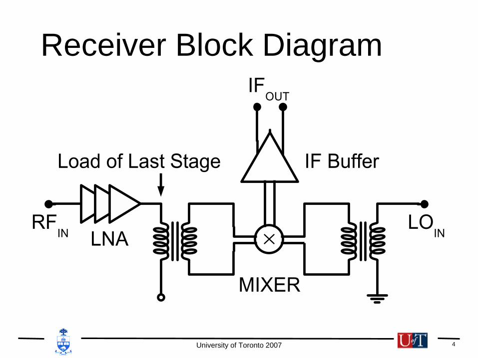
Receiver Block Diagram

University of Toronto 2007 5
• Inductive (series-series) feedback LNA
• Input matched by LG and LS
• Noise impedance matched by transistor sizing and biasingSGSTIN RRLfZ ++=ℜ π2}{
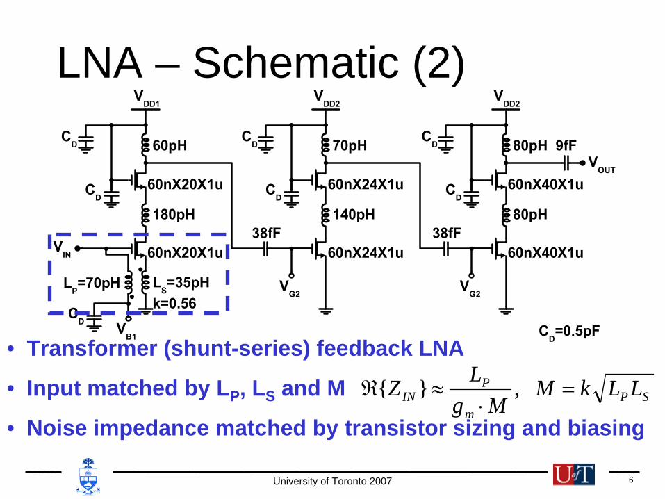
LNA – Schematic
University of Toronto 2007 6
• Transformer (shunt-series) feedback LNA
• Input matched by LP , LS and M
• Noise impedance matched by transistor sizing and biasingSP
m
PIN LLkM
MgLZ =⋅
≈ℜ ,}{
LNA – Schematic (2)

University of Toronto 2007 7
• S11 , Γopt < -10 dB from 74-100 GHz for both designs
50 60 70 80 90 100FREQUENCY [GHz]
-30 -30
-25 -25
-20 -20
-15 -15
-10 -10
-5 -5
0 0
5 5
10 10
15 15
20 20
[dB
]
S21S11Γopt
NF50NFMIN
50 60 70 80 90 100FREQUENCY [GHz]
-30 -30
-25 -25
-20 -20
-15 -15
-10 -10
-5 -5
0 0
5 5
10 10
15 15
20 20
[dB
]
S21S11Γopt
NF50NFMIN
LNA – Simulation
ind-feedback xfmr-feedback

University of Toronto 2007 8
Mixer – Schematic
• Gilbert cell mixer with inductive broad-banding

University of Toronto 2007 9
Fabrication• 65-nm GP/LP digital CMOS process
• 7 metal layers
• GP n-MOSFETs (80×60nm×1μm) with gate contacted on one side: fT /fMAX =170 GHz/200 GHz at VDS = 0.7 V
• GP MOSFETs 30% faster than LP MOSFETs and require lower VGS and VDS → lower power
• Gate leakage does not affect mm-wave performance

University of Toronto 2007 10
LNA breakouts – Die Photos
IND-feedback XFMR-feedback
IND
XFMR
490 um x 300um (pad) 120 um x 170 um (core)
University of Toronto 2007 11
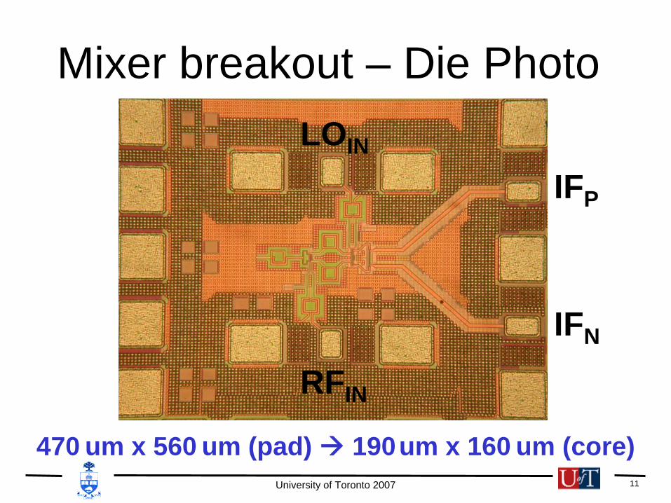
Mixer breakout – Die Photo
RFIN
LOIN
IFP
IFN
470 um x 560 um (pad) 190um x 160 um (core)

University of Toronto 2007 12
Receiver – Die Photos
IND-feedback Receiver XFMR-feedback Receiver460 um x 500 um (pad) 160 um x 370 um (core)

University of Toronto 2007 13
60 65 70 75 80 85 90 95FREQUENCY (GHz)
-30 -30
-25 -25
-20 -20
-15 -15
-10 -10
-5 -5
0 0
5 5
10 10
15 15
S21
, S11
(d
B)
S21 (sim.)S21 (meas.)S11 (sim.)S11 (meas.)
60 65 70 75 80 85 90 95FREQUENCY (GHz)
-30 -30
-25 -25
-20 -20
-15 -15
-10 -10
-5 -5
0 0
5 5
10 10
15 15
S21
, S11
(d
B)
S21 (sim.) S21 (meas.)S11 (sim.)S11 (meas.)
Meas. LNA – 1st Spin
ind-feedback xfmr-feedback
• Requires 2.2 V VDD for 8 – 9 dB gain
• 4 – 5 dB below simulation

University of Toronto 2007 14
Measurements for 2nd Spin with Modified Layout
Series resistance in ground metallization of LNA was found in the first spin.
A second spin of the design was fabricated with:• Wider metal lines in ground mesh at top level
• Increased number of vias (even between M5 and M6)
• LNA inductance values adjusted to match @ 80 GHz

University of Toronto 2007 15
65 70 75 80 85 90 95FREQUENCY [GHz]
0
2
4
6
8
10
12
14
16
18
20
22
GA
IN [
dB
]
VDD=1.8V (1st
spin)
VDD=2.2V (1st
spin)
VDD=1.2V (2nd
spin)
VDD=1.5V (2nd
spin)
VDD=1.8V (2nd
spin)
65 70 75 80 85 90 95FREQUENCY [GHz]
0
2
4
6
8
10
12
14
16
18
20
22
GA
IN [
dB
]
VDD=1.8V (1st
spin)
VDD=2.2V (1st
spin)
VDD=1.2V (2nd
spin)
VDD=1.5V (2nd
spin)
VDD=1.8V (2nd
spin)
Meas. LNA – 2nd Spin
• Measured gain @ 1.5 V VDD = 13 dB
ind-feedback xfmr-feedback

University of Toronto 2007 16
65 70 75 80 85 90 95FREQUENCY (GHz)
-40 -40
-30 -30
-20 -20
-10 -10
0 0
10 10
20 20
S21
, S11
(d
B)
S21 (sim.)S11 (sim.)S21 (meas.)S11 (meas.)
65 70 75 80 85 90 95FREQUENCY (GHz)
-40 -40
-30 -30
-20 -20
-10 -10
0 0
10 10
20 20
S21
, S11
(d
B)
S21 (sim.)S11 (sim.)S21 (meas.)S11 (meas.)
2nd Spin LNA – meas. vs sims.
• Meas. gain @ VDD = 1.5 V is 1 – 2 dB below sims.
• S11 < -20 dB from 80 – 90 GHz (xfmr-feedback)
ind-feedback xfmr-feedback

University of Toronto 2007 17
50 60 70 80 90 100FREQUENCY [GHz]
-20 -20
-18 -18
-16 -16
-14 -14
-12 -12
-10 -10
-8 -8
-6 -6
-4 -4
-2 -2
0 0
[dB
]
S11S22S21MAG
Meas. Transformer S-params.
• MAG (loss) < -2 dB between 75 – 95 GHz

University of Toronto 2007 18
70 75 80 85 90 95 100RF FREQUENCY [GHz]
0
1
2
3
4
5
6
7
8
9C
ON
VE
RS
ION
GA
IN [
dB
]
VDD=1.5VVDD=1.8VVDD=1.8V (sim.)
IF = 1GHz
Meas. Mixer – Conversion Gain
• 1 – 2 dB below simulation

University of Toronto 2007 19
74 76 78 80 82 84 86 88 90 92 94 96 98RF FREQUENCY [GHz]
0
2
4
6
8
10
12
14
16
NO
ISE
FIG
UR
E [
dB
]
NFMIXER, VDD=1.5VNFMIXER, VDD=1.8V
IF = 1GHz
Meas. Mixer – NFDSB
• Includes ~2 dB transformer loss
• Lowest NFDSB mixer at 80 – 90 GHz in silicon

University of Toronto 2007 20
0 5 10 15 20IF FREQUENCY [GHz]
0 0
5 5
10 10
15 15
20 20
NF
DS
B [
dB
]
VDD=1.2VVDD=1.5VVDD=1.8V
0 5 10 15 20IF FREQUENCY [GHz]
0 0
5 5
10 10
15 15
20 20
CO
NV
ER
SIO
N G
AIN
[d
B]
VDD=1.2VVDD=1.5VVDD=1.8V
Meas. Rx Gain, NFDSB vs IF
• NFDSB ~7 – 8 dB, LO @ 89 GHzXFMR-feedback RCVR
University of Toronto 2007 21
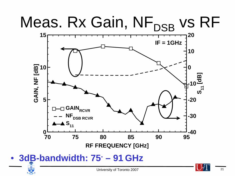
70 75 80 85 90 95RF FREQUENCY [GHz]
0
5
10
15G
AIN
, NF
[d
B]
GAINRCVRNFDSB RCVR
-40
-30
-20
-10
0
10
20
S11
[d
B]
S11
IF = 1GHz
Meas. Rx Gain, NFDSB vs RF
• 3dB-bandwidth: 75- – 91 GHz

University of Toronto 2007 22
-30 -25 -20 -15 -10 -5 0PIN [dBm]
-15
-10
-5
0
5
10
15G
AIN
[d
B]
-15
-10
-5
0
5
10
15
PO
UT [
dB
m]
LO = 75GHzRF = 80GHz
P1dB = -16.2dBm
• LO @ 75 GHz due to equipment limitation
Receiver – P1dB

University of Toronto 2007 23
75 80 85 90FREQUENCY [GHz]
0 0
2 2
4 4
6 6
8 8
10 10
12 12
14 14
16 16
[dB
]
GAIN, VDD=1.5VGAIN, VDD=1.8VNF50, VDD=1.5VNF50, VDD=1.8V
LNA
MIXERRCVRLNA
MIXERRCVRLNA
GFFF
GGG1−
−=
−=Estimated LNA NF
XFMR-feedback LNA
• LNA gain peaks at frequency higher than measured (output pad capacitance removed)
• LNA NF50 ~6 – 7 dB

University of Toronto 2007 24
2nd
Spin
1.2 24 11.1 20 48 6.1 9 – 10< -10
(74-95+ GHz)1.5 34 13.4 30 71 13.6 7 – 8
1.8 48 14.9 45 104 17.7 6 – 7
1st
Spin
VDD
[V]
LNA IF Buffer Receiver
Pdiss
[mW]
Gain
[dB]
Pdiss
[mW]
Pdiss
[mW]
Gain
[dB]
NF
[dB]
S11
[dB]
1.8 38 5.8 47 95 11.6 9 – 10 < -10
(80-95+ GHz)2.2 57 7.8 75 150 13.5 8 – 9
Summary of Results
• Dramatic increase in performance just with better top-level ground mesh and vias
• ~ ½ of Pdiss used in IF buffer to drive 50Ω
off-chip

University of Toronto 2007 25
Conclusion• 74 – 94 GHz receiver with 8 dB NF and 13 dB gain
demonstrated in 65 nm GP CMOS technology.
• Inductive-feedback and transformer-feedback LNA topologies presented:
• Similar performance achieved by different matching procedures
• Layout style significantly affects circuit performance.
• Post-layout simulation at top-level, with ground mesh must be carried out.

University of Toronto 2007 26
Acknowledgement• Katya Laskin for measurements on the second-spin
• Alex Tomkins for inductor and transformer measurements
• Jaro Pristupa and CMC for CAD tools
• Bernard Sautreuil of STM for facilitating the technology access
• CITO for funding
• ECTI, NSERC, CFI and OIF for equipment

University of Toronto 2007 27
• S11 matched at 93 GHz for inductive-feedback LNA (increase LG )
65 70 75 80 85 90 95FREQUENCY [GHz]
-30 -30
-25 -25
-20 -20
-15 -15
-10 -10
-5 -5
0 0
5 5
10 10
15 15
20 20
S11
, S21
[d
B]
VDD=1.2VVDD=1.5VVDD=1.8V
65 70 75 80 85 90 95FREQUENCY [GHz]
-30 -30
-25 -25
-20 -20
-15 -15
-10 -10
-5 -5
0 0
5 5
10 10
15 15
20 20
S11
, S21
[d
B]
VDD=1.2VVDD=1.5VVDD=1.8V
2nd spin LNA – Meas. Gain
IND-feedback LNA XFMR-feedback LNA

University of Toronto 2007 28
-15 -10 -5 0 5
LO POWER [dBm]
-5
0
5
10
15
20
CO
NV
ER
SIO
N G
AIN
[d
B]
VDD=1.8VVDD=2.0VVDD=2.2V
LO = 85GHzRF = 84.5GHz
-15 -10 -5 0 5
LO POWER [dBm]
-5
0
5
10
15
20
CO
NV
ER
SIO
N G
AIN
[d
B]
VDD=1.8VVDD=2.0VVDD=2.2V
VDD=1.2V (2nd
spin)
VDD=1.5V (2nd
spin)
VDD=1.8V (2nd
spin)
LO = 85GHzRF = 84.5GHz
ind-feedback xfmr-feedback
Receiver – vs LO Power
• Requires 2 – 3 dBm (1st spin) and > 5 dBm (2nd spin) LO power

University of Toronto 2007 29
-30 -25 -20 -15 -10PIN [dBm]
-25
-20
-15
-10
-5
0
5
PO
UT [
dB
m]
0
2
4
6
8
10
12
GA
IN [
dB
]
LO=77GHz, RF=75GHz
-30 -25 -20 -15 -10PIN [dBm]
-25
-20
-15
-10
-5
0
5
PO
UT [
dB
m]
0
2
4
6
8
10
12
GA
IN [
dB
]
LO=77GHz, RF=75GHz
IND-feedback Receiver XFMR-feedback Receiver
Receiver – P1dB
• RF at 75 GHz due to equipment limitation