54sx family fpgas - microsemi
TRANSCRIPT

v3.2
SX Family FPGAs
Leading Edge Performance• 320 MHz Internal Performance• 3.7 ns Clock-to-Out (Pin-to-Pin)• 0.1 ns Input Setup• 0.25 ns Clock Skew
Specifications• 12,000 to 48,000 System Gates• Up to 249 User-Programmable I/O Pins• Up to 1,080 Flip-Flops• 0.35 µ CMOS
Features• 66 MHz PCI• CPLD and FPGA Integration• Single-Chip Solution• 100% Resource Utilization with 100% Pin Locking• 3.3 V and 5.0 V Operation with 5.0 V Input Tolerance• Very Low Power Consumption• Deterministic, User-Controllable Timing• Unique In-System Diagnostic and Debug Capability
with Silicon Explorer II• Boundary Scan Testing in Compliance with IEEE
Standard 1149.1 (JTAG)• Secure Programming Technology Prevents Reverse
Engineering and Design Theft
™
eu
SX Product ProfileDevice A54SX08 A54SX16 A54SX16P A54SX32
CapacityTypical GatesSystem Gates
8,00012,000
16,00024,000
16,00024,000
32,00048,000
Logic ModulesCombinatorial Cells
768512
1,452924
1,452924
2,8801,800
Register Cells (Dedicated Flip-Flops) 256 528 528 1,080
Maximum User I/Os 130 175 175 249
Clocks 3 3 3 3
JTAG Yes Yes Yes Yes
PCI – – Yes –
Clock-to-Out 3.7 ns 3.9 ns 4.4 ns 4.6 ns
Input Setup (external) 0.8 ns 0.5 ns 0.5 ns 0.1 ns
Speed Grades Std, –1, –2, –3 Std, –1, –2, –3 Std, –1, –2, –3 Std, –1, –2, –3
Temperature Grades C, I, M C, I, M C, I, M C, I, M
Packages (by pin count)PLCCPQFPVQFPTQFPPBGAFBGA
84208100
144, 176–
144
–208100176
––
–208100
144, 176––
–208
–144, 176313, 329
–
June 2006 i© 2006 Actel Corporation See the Actel website for the latest version of the datasheet.

SX Family FPGAs
Ordering Information
Plastic Device Resources
Part Number A54SX08 = 12,000 System Gates A54SX16 = 24,000 System Gates A54SX16P = 24,000 System Gates A54SX32 = 48,000 System Gates
Speed Grade Blank = Standard Speed –1 = Approximately 15% Faster than Standard –2 = Approximately 25% Faster than Standard –3 = Approximately 35% Faster than Standard
Package Type BG = Ball Grid Array PL = Plastic Leaded Chip Carrier PQ = Plastic Quad Flat Pack TQ = Thin (1.4 mm) Quad Flat Pack VQ = Very Thin (1.0 mm) Quad Flat Pack FG = Fine Pitch Ball Grid Array (1.0 mm)
Package Lead Count
Application (Temperature Range) Blank = Commercial (0 to +70˚C) I = Industrial (–40 to +85˚C) M = Military (–55 to +125˚C) PP = Pre-production
A54SX16 P 2 PQ 208
Blank = Not PCI Compliant P = PCI Compliant
G
Lead-Free Packaging Blank = Standard Packaging G = RoHS Compliant Packaging
–
Device
User I/Os (including clock buffers)
PLCC 84-Pin
VQFP100-Pin
PQFP208-Pin
TQFP144-Pin
TQFP176-Pin
PBGA 313-Pin
PBGA 329-Pin
FBGA 144-Pin
A54SX08 69 81 130 113 128 – – 111
A54SX16 – 81 175 – 147 – – –
A54SX16P – 81 175 113 147 – – –
A54SX32 – – 174 113 147 249 249 –
Note: Package Definitions (Consult your local Actel sales representative for product availability):PLCC = Plastic Leaded Chip CarrierPQFP = Plastic Quad Flat PackTQFP = Thin Quad Flat PackVQFP = Very Thin Quad Flat PackPBGA = Plastic Ball Grid ArrayFBGA = Fine Pitch (1.0 mm) Ball Grid Array
ii v3.2

Table of Contents
SX Family FPGAs
SX Family FPGAsGeneral Description . . . . . . . . . . . . . . . . . . . . . . . . . . . . . . . . . . . . . . . . . . . . . . . . . . 1-1
SX Family Architecture . . . . . . . . . . . . . . . . . . . . . . . . . . . . . . . . . . . . . . . . . . . . . . . . 1-1
Programming . . . . . . . . . . . . . . . . . . . . . . . . . . . . . . . . . . . . . . . . . . . . . . . . . . . . . . . 1-7
3.3 V / 5 V Operating Conditions . . . . . . . . . . . . . . . . . . . . . . . . . . . . . . . . . . . . . . . 1-7
PCI Compliance for the SX Family . . . . . . . . . . . . . . . . . . . . . . . . . . . . . . . . . . . . . . . 1-9
A54SX16P AC Specifications for (PCI Operation) . . . . . . . . . . . . . . . . . . . . . . . . . . 1-10
A54SX16P DC Specifications (3.3 V PCI Operation) . . . . . . . . . . . . . . . . . . . . . . . . 1-12
A54SX16P AC Specifications (3.3 V PCI Operation) . . . . . . . . . . . . . . . . . . . . . . . . 1-13
Power-Up Sequencing . . . . . . . . . . . . . . . . . . . . . . . . . . . . . . . . . . . . . . . . . . . . . . . 1-15
Power-Down Sequencing . . . . . . . . . . . . . . . . . . . . . . . . . . . . . . . . . . . . . . . . . . . . . 1-15
Evaluating Power in SX Devices . . . . . . . . . . . . . . . . . . . . . . . . . . . . . . . . . . . . . . . . 1-16
SX Timing Model . . . . . . . . . . . . . . . . . . . . . . . . . . . . . . . . . . . . . . . . . . . . . . . . . . . 1-21
Timing Characteristics . . . . . . . . . . . . . . . . . . . . . . . . . . . . . . . . . . . . . . . . . . . . . . . 1-23
Package Pin Assignments84-Pin PLCC . . . . . . . . . . . . . . . . . . . . . . . . . . . . . . . . . . . . . . . . . . . . . . . . . . . . . . . . 2-1
208-Pin PQFP . . . . . . . . . . . . . . . . . . . . . . . . . . . . . . . . . . . . . . . . . . . . . . . . . . . . . . . 2-3
144-Pin TQFP . . . . . . . . . . . . . . . . . . . . . . . . . . . . . . . . . . . . . . . . . . . . . . . . . . . . . . . 2-7
176-Pin TQFP . . . . . . . . . . . . . . . . . . . . . . . . . . . . . . . . . . . . . . . . . . . . . . . . . . . . . . . 2-10
100-Pin VQFP . . . . . . . . . . . . . . . . . . . . . . . . . . . . . . . . . . . . . . . . . . . . . . . . . . . . . . 2-14
313-Pin PBGA . . . . . . . . . . . . . . . . . . . . . . . . . . . . . . . . . . . . . . . . . . . . . . . . . . . . . . 2-16
329-Pin PBGA . . . . . . . . . . . . . . . . . . . . . . . . . . . . . . . . . . . . . . . . . . . . . . . . . . . . . . 2-19
144-Pin FBGA . . . . . . . . . . . . . . . . . . . . . . . . . . . . . . . . . . . . . . . . . . . . . . . . . . . . . . 2-23
Datasheet InformationList of Changes . . . . . . . . . . . . . . . . . . . . . . . . . . . . . . . . . . . . . . . . . . . . . . . . . . . . . . 3-1
Datasheet Categories . . . . . . . . . . . . . . . . . . . . . . . . . . . . . . . . . . . . . . . . . . . . . . . . . 3-1
International Traffic in Arms Regulations (ITAR) and Export Administration Regulations (EAR) . . . . . . . . . . . . . . . . . . . . . . . . . . . . . . . . . . . . . . . . . . . . . . . . . . . . 3-1
v3.2 iii


SX Family FPGAs
SX Family FPGAs
General DescriptionThe Actel SX family of FPGAs features a sea-of-modulesarchitecture that delivers device performance andintegration levels not currently achieved by any otherFPGA architecture. SX devices greatly simplify designtime, enable dramatic reductions in design costs andpower consumption, and further decrease time tomarket for performance-intensive applications.
The Actel SX architecture features two types of logicmodules, the combinatorial cell (C-cell) and the registercell (R-cell), each optimized for fast and efficientmapping of synthesized logic functions. The routing andinterconnect resources are in the metal layers above thelogic modules, providing optimal use of silicon. Thisenables the entire floor of the device to be spanned withan uninterrupted grid of fine-grained, synthesis-friendlylogic modules (or “sea-of-modules”), which reduces thedistance signals have to travel between logic modules. Tominimize signal propagation delay, SX devices employboth local and general routing resources. The high-speedlocal routing resources (DirectConnect and FastConnect)enable very fast local signal propagation that is optimalfor fast counters, state machines, and datapath logic.The general system of segmented routing tracks allowsany logic module in the array to be connected to anyother logic or I/O module. Within this system,propagation delay is minimized by limiting the numberof antifuse interconnect elements to five (90 percent ofconnections typically use only three antifuses). Theunique local and general routing structure featured inSX devices gives fast and predictable performance,allows 100 percent pin-locking with full logic utilization,enables concurrent PCB development, reduces designtime, and allows designers to achieve performance goalswith minimum effort.
Further complementing SX’s flexible routing structure isa hardwired, constantly loaded clock network that hasbeen tuned to provide fast clock propagation withminimal clock skew. Additionally, the high performanceof the internal logic has eliminated the need to embedlatches or flip-flops in the I/O cells to achieve fast clock-to-out or fast input setup times. SX devices have easy touse I/O cells that do not require HDL instantiation,facilitating design reuse and reducing design andverification time.
SX Family ArchitectureThe SX family architecture was designed to satisfy next-generation performance and integration requirementsfor production-volume designs in a broad range ofapplications.
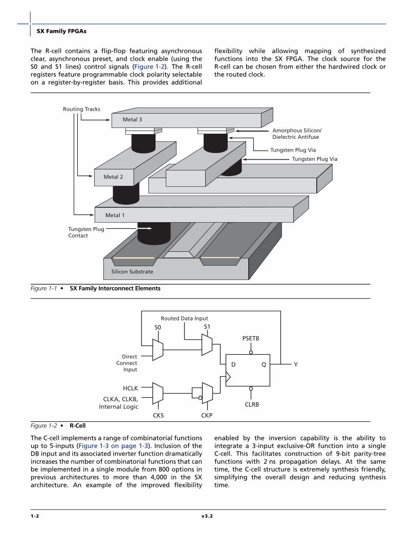
Programmable Interconnect ElementThe SX family provides efficient use of silicon by locatingthe routing interconnect resources between the Metal 2(M2) and Metal 3 (M3) layers (Figure 1-1 on page 1-2).This completely eliminates the channels of routing andinterconnect resources between logic modules (asimplemented on SRAM FPGAs and previous generationsof antifuse FPGAs), and enables the entire floor of thedevice to be spanned with an uninterrupted grid of logicmodules.
Interconnection between these logic modules is achievedusing The Actel patented metal-to-metal programmableantifuse interconnect elements, which are embeddedbetween the M2 and M3 layers. The antifuses arenormally open circuit and, when programmed, form apermanent low-impedance connection.
The extremely small size of these interconnect elementsgives the SX family abundant routing resources andprovides excellent protection against design pirating.Reverse engineering is virtually impossible because it isextremely difficult to distinguish between programmedand unprogrammed antifuses, and there is noconfiguration bitstream to intercept.
Additionally, the interconnect elements (i.e., theantifuses and metal tracks) have lower capacitance andlower resistance than any other device of similarcapacity, leading to the fastest signal propagation in theindustry.
Logic Module DesignThe SX family architecture is described as a “sea-of-modules” architecture because the entire floor of thedevice is covered with a grid of logic modules withvirtually no chip area lost to interconnect elements orrouting. The Actel SX family provides two types of logicmodules, the register cell (R-cell) and the combinatorialcell (C-cell).
v3.2 1-1
SX Family FPGAs
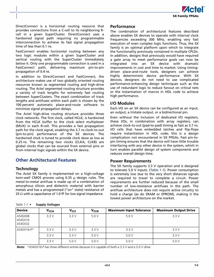
The R-cell contains a flip-flop featuring asynchronousclear, asynchronous preset, and clock enable (using theS0 and S1 lines) control signals (Figure 1-2). The R-cellregisters feature programmable clock polarity selectableon a register-by-register basis. This provides additional
flexibility while allowing mapping of synthesizedfunctions into the SX FPGA. The clock source for theR-cell can be chosen from either the hardwired clock orthe routed clock.
The C-cell implements a range of combinatorial functionsup to 5-inputs (Figure 1-3 on page 1-3). Inclusion of theDB input and its associated inverter function dramaticallyincreases the number of combinatorial functions that canbe implemented in a single module from 800 options inprevious architectures to more than 4,000 in the SXarchitecture. An example of the improved flexibility
enabled by the inversion capability is the ability tointegrate a 3-input exclusive-OR function into a singleC-cell. This facilitates construction of 9-bit parity-treefunctions with 2 ns propagation delays. At the sametime, the C-cell structure is extremely synthesis friendly,simplifying the overall design and reducing synthesistime.
Figure 1-1 • SX Family Interconnect Elements
Figure 1-2 • R-Cell
Silicon Substrate
Tungsten PlugContact
Metal 1
Metal 2
Metal 3
Routing Tracks
Amorphous Silicon/Dielectric Antifuse
Tungsten Plug Via
Tungsten Plug Via
DirectConnect
Input
CLKA, CLKB,Internal Logic
HCLK
CKS CKP
CLRB
PSETB
YD Q
Routed Data Input
S0 S1
1-2 v3.2

SX Family FPGAs
Chip ArchitectureThe SX family chip architecture provides a uniqueapproach to module organization and chip routing thatdelivers the best register/logic mix for a wide variety ofnew and emerging applications.
Module OrganizationActel has arranged all C-cell and R-cell logic modules intohorizontal banks called clusters. There are two types ofclusters: Type 1 contains two C-cells and one R-cell, whileType 2 contains one C-cell and two R-cells.
To increase design efficiency and device performance,Actel has further organized these modules intoSuperClusters (Figure 1-4). SuperCluster 1 is a two-widegrouping of Type 1 clusters. SuperCluster 2 is a two-widegroup containing one Type 1 cluster and one Type 2cluster. SX devices feature more SuperCluster 1 modulesthan SuperCluster 2 modules because designers typicallyrequire significantly more combinatorial logic than flip-flops.
Figure 1-3 • C-Cell
Figure 1-4 • Cluster Organization
D0
D1
D2
D3
DB
A0 B0 A1 B1
Sa Sb
Y
Type 1 SuperCluster Type 2 SuperCluster
Cluster 1 Cluster 2 Cluster 2 Cluster 1
R-Cell C-Cell
D0
D1
D2
D3
DB
A0 B0 A1 B1
Sa Sb
Y
DirectConnect
Input
CLKA, CLKB,Internal Logic
HCLK
CKS CKP
CLRB
PSETB
YD Q
Routed Data Input
S0 S1
v3.2 1-3

SX Family FPGAs
Routing ResourcesClusters and SuperClusters can be connected through the use of two innovative local routing resources calledFastConnect and DirectConnect, which enable extremely fast and predictable interconnection of modules withinclusters and SuperClusters (Figure 1-5 and Figure 1-6). This routing architecture also dramatically reduces the numberof antifuses required to complete a circuit, ensuring the highest possible performance.
Figure 1-5 • DirectConnect and FastConnect for Type 1 SuperClusters
Figure 1-6 • DirectConnect and FastConnect for Type 2 SuperClusters
Routing Segments• Typically 2 antifuses• Max. 5 antifuses
FastConnect• One antifuse• 0.4 ns routing delay
DirectConnect• No antifuses• 0.1 ns routing delay
Routing Segments• Typically 2 antifuses• Max. 5 antifuses
FastConnect• One antifuse• 0.4 ns routing delay
DirectConnect• No antifuses• 0.1 ns routing delay
1-4 v3.2
SX Family FPGAs
DirectConnect is a horizontal routing resource thatprovides connections from a C-cell to its neighboring R-cell in a given SuperCluster. DirectConnect uses ahardwired signal path requiring no programmableinterconnection to achieve its fast signal propagationtime of less than 0.1 ns.
FastConnect enables horizontal routing between anytwo logic modules within a given SuperCluster andvertical routing with the SuperCluster immediatelybelow it. Only one programmable connection is used in aFastConnect path, delivering maximum pin-to-pinpropagation of 0.4 ns.
In addition to DirectConnect and FastConnect, thearchitecture makes use of two globally oriented routingresources known as segmented routing and high-driverouting. The Actel segmented routing structure providesa variety of track lengths for extremely fast routingbetween SuperClusters. The exact combination of tracklengths and antifuses within each path is chosen by the100 percent automatic place-and-route software tominimize signal propagation delays.
The Actel high-drive routing structure provides threeclock networks. The first clock, called HCLK, is hardwiredfrom the HCLK buffer to the clock select multiplexer(MUX) in each R-cell. This provides a fast propagationpath for the clock signal, enabling the 3.7 ns clock-to-out(pin-to-pin) performance of the SX devices. Thehardwired clock is tuned to provide clock skew as low as0.25 ns. The remaining two clocks (CLKA, CLKB) areglobal clocks that can be sourced from external pins orfrom internal logic signals within the SX device.
Other Architectural Features
TechnologyThe Actel SX family is implemented on a high-voltagetwin-well CMOS process using 0.35 µ design rules. Themetal-to-metal antifuse is made up of a combination ofamorphous silicon and dielectric material with barriermetals and has a programmed ("on" state) resistance of25 Ω with a capacitance of 1.0 fF for low signal impedance.
PerformanceThe combination of architectural features describedabove enables SX devices to operate with internal clockfrequencies exceeding 300 MHz, enabling very fastexecution of even complex logic functions. Thus, the SXfamily is an optimal platform upon which to integratethe functionality previously contained in multiple CPLDs.In addition, designs that previously would have requireda gate array to meet performance goals can now beintegrated into an SX device with dramaticimprovements in cost and time to market. Using timing-driven place-and-route tools, designers can achievehighly deterministic device performance. With SXdevices, designers do not need to use complicatedperformance-enhancing design techniques such as theuse of redundant logic to reduce fanout on critical netsor the instantiation of macros in HDL code to achievehigh performance.
I/O ModulesEach I/O on an SX device can be configured as an input,an output, a tristate output, or a bidirectional pin.
Even without the inclusion of dedicated I/O registers,these I/Os, in combination with array registers, canachieve clock-to-out (pad-to-pad) timing as fast as 3.7 ns.I/O cells that have embedded latches and flip-flopsrequire instantiation in HDL code; this is a designcomplication not encountered in SX FPGAs. Fast pin-to-pin timing ensures that the device will have little troubleinterfacing with any other device in the system, which inturn enables parallel design of system components andreduces overall design time.
Power RequirementsThe SX family supports 3.3 V operation and is designedto tolerate 5.0 V inputs. (Table 1-1). Power consumptionis extremely low due to the very short distances signalsare required to travel to complete a circuit. Powerrequirements are further reduced because of the smallnumber of low-resistance antifuses in the path. Theantifuse architecture does not require active circuitry tohold a charge (as do SRAM or EPROM), making it thelowest power architecture on the market.
Table 1-1 • Supply Voltages
Device VCCA VCCI VCCR Maximum Input Tolerance Maximum Output Drive
A54SX08A54SX16A54SX32
3.3 V 3.3 V 5.0 V 5.0 V 3.3 V
A54SX16-P* 3.3 V 3.3 V 3.3 V 3.3 V 3.3 V
3.3 V 3.3 V 5.0 V 5.0 V 3.3 V
3.3 V 5.0 V 5.0 V 5.0 V 5.0 V
Note: *A54SX16-P has three different entries because it is capable of both a 3.3 V and a 5.0 V drive.
v3.2 1-5

SX Family FPGAs
Boundary Scan Testing (BST)All SX devices are IEEE 1149.1 compliant. SX devices offersuperior diagnostic and testing capabilities by providingBoundary Scan Testing (BST) and probing capabilities.These functions are controlled through the special testpins in conjunction with the program fuse. Thefunctionality of each pin is described in Table 1-2. In thededicated test mode, TCK, TDI, and TDO are dedicatedpins and cannot be used as regular I/Os. In flexible mode,TMS should be set HIGH through a pull-up resistor of10 kΩ. TMS can be pulled LOW to initiate the testsequence.
The program fuse determines whether the device is indedicated or flexible mode. The default (fuse not blown)is flexible mode.
Dedicated Test ModeIn Dedicated mode, all JTAG pins are reserved for BST;designers cannot use them as regular I/Os. An internalpull-up resistor is automatically enabled on both TMSand TDI pins, and the TMS pin will function as defined inthe IEEE 1149.1 (JTAG) specification.
To select Dedicated mode, users need to reserve the JTAGpins in Actel's Designer software by checking the"Reserve JTAG" box in "Device Selection Wizard"(Figure 1-7). JTAG pins comply with LVTTL/TTL I/Ospecification regardless of whether they are used as auser I/O or a JTAG I/O. Refer to the Table 1-5 on page 1-8for detailed specifications.
Development Tool SupportThe SX family of FPGAs is fully supported by both theActel Libero® Integrated Design Environment (IDE) andDesigner FPGA Development software. Actel Libero IDEis a design management environment, seamlesslyintegrating design tools while guiding the user throughthe design flow, managing all design and log files, andpassing necessary design data among tools. Libero IDEallows users to integrate both schematic and HDLsynthesis into a single flow and verify the entire designin a single environment. Libero IDE includes Synplify® forActel from Synplicity®, ViewDraw® for Actel fromMentor Graphics®, ModelSim® HDL Simulator fromMentor Graphics, WaveFormer Lite™ fromSynaptiCAD™, and Designer software from Actel. Referto the Libero IDE flow diagram (located on the Actelwebsite) for more information.
Actel Designer software is a place-and-route tool andprovides a comprehensive suite of backend support toolsfor FPGA development. The Designer software includestiming-driven place-and-route, and a world-classintegrated static timing analyzer and constraints editor.With the Designer software, a user can select and lockpackage pins while only minimally impacting the resultsof place-and-route. Additionally, the back-annotationflow is compatible with all the major simulators, and thesimulation results can be cross-probed with SiliconExplorer II, Actel integrated verification and logicanalysis tool. Another tool included in the Designersoftware is the SmartGen core generator, which easilycreates popular and commonly used logic functions forimplementation into your schematic or HDL design. ActelDesigner software is compatible with the most popularFPGA design entry and verification tools from companiessuch as Mentor Graphics, Synplicity, Synopsys®, andCadence® Design Systems. The Designer software isavailable for both the Windows® and UNIX® operatingsystems.
Probe Circuit Control PinsThe Silicon Explorer II tool uses the boundary scan ports(TDI, TCK, TMS, and TDO) to select the desired nets forverification. The selected internal nets are assigned tothe PRA/PRB pins for observation. Figure 1-8 on page 1-7illustrates the interconnection between Silicon Explorer IIand the FPGA to perform in-circuit verification.
Design ConsiderationsThe TDI, TCK, TDO, PRA, and PRB pins should not be usedas input or bidirectional ports. Because these pins areactive during probing, critical signals input throughthese pins are not available while probing. In addition,the Security Fuse should not be programmed becausedoing so disables the Probe Circuitry.
Table 1-2 • Boundary Scan Pin Functionality
Program Fuse Blown (Dedicated Test Mode)
Program Fuse Not Blown (Flexible Mode)
TCK, TDI, TDO are dedicatedBST pins.
TCK, TDI, TDO are flexible andmay be used as I/Os.
No need for pull-up resistor forTMS
Use a pull-up resistor of 10 kΩon TMS.
Figure 1-7 • Device Selection Wizard
1-6 v3.2

SX Family FPGAs
ProgrammingDevice programming is supported through SiliconSculptor series of programmers. In particular, SiliconSculptor II are compact, robust, single-site and multi-sitedevice programmer for the PC.
With standalone software, Silicon Sculptor II allowsconcurrent programming of multiple units from thesame PC, ensuring the fastest programming timespossible. Each fuse is subsequently verified by SiliconSculptor II to insure correct programming. In addition,integrity tests ensure that no extra fuses areprogrammed. Silicon Sculptor II also provides extensivehardware self-testing capability.
The procedure for programming an SX device usingSilicon Sculptor II are as follows:
1. Load the .AFM file
2. Select the device to be programmed
3. Begin programming
When the design is ready to go to production, Acteloffers device volume-programming services eitherthrough distribution partners or via in-houseprogramming from the factory.
For more details on programming SX devices, refer to theProgramming Antifuse Devices application note and theSilicon Sculptor II User's Guide.
3.3 V / 5 V Operating Conditions
Figure 1-8 • Probe Setup
SX FPGATDITCK
TDO
TMS
PRAPRB
Serial Connection
16 Channels
SiliconExplorer II
Table 1-3 • Absolute Maximum Ratings1
Symbol Parameter Limits Units
VCCR2 DC Supply Voltage3 –0.3 to + 6.0 V
VCCA2 DC Supply Voltage –0.3 to + 4.0 V
VCCI2 DC Supply Voltage (A54SX08, A54SX16, A54SX32) –0.3 to + 4.0 V
VCCI2 DC Supply Voltage (A54SX16P) –0.3 to + 6.0 V
VI Input Voltage –0.5 to + 5.5 V
VO Output Voltage –0.5 to + 3.6 V
IIO I/O Source Sink Current3 –30 to + 5.0 mA
TSTG Storage Temperature –65 to +150 °C
Notes:
1. Stresses beyond those listed under “Absolute Maximum Ratings” may cause permanent damage to the device. Exposure to absolutemaximum rated conditions for extended periods may affect device reliability. Device should not be operated outside theRecommended Operating Conditions.
2. VCCR in the A54SX16P must be greater than or equal to VCCI during power-up and power-down sequences and during normaloperation.
3. Device inputs are normally high impedance and draw extremely low current. However, when input voltage is greater than VCC +0.5 V or less than GND – 0.5 V, the internal protection diodes will forward-bias and can draw excessive current.
v3.2 1-7

SX Family FPGAs
Table 1-4 • Recommended Operating Conditions
Parameter Commercial Industrial Military Units
Temperature Range* 0 to + 70 –40 to + 85 –55 to +125 °C
3.3 V Power Supply Tolerance ±10 ±10 ±10 %VCC
5.0 V Power Supply Tolerance ±5 ±10 ±10 %VCC
Note: *Ambient temperature (TA) is used for commercial and industrial; case temperature (TC) is used for military.
Table 1-5 • Electrical Specifications
Commercial Industrial
UnitsSymbol Parameter Min. Max. Min. Max.
VOH (IOH = –20 µA) (CMOS)
(IOH = –8 mA) (TTL)
(IOH = –6 mA) (TTL)
(VCCI – 0.1)
2.4
VCCI
VCCI
(VCCI – 0.1)
2.4
VCCI
VCCI
V
VOL (IOL= 20 µA) (CMOS)
(IOL = 12 mA) (TTL)
(IOL = 8 mA) (TTL)
0.10
0.50
0.50
V
VIL 0.8 0.8 V
VIH 2.0 2.0 V
tR, tF Input Transition Time tR, tF 50 50 ns
CIO CIO I/O Capacitance 10 10 pF
ICC Standby Current, ICC 4.0 4.0 mA
ICC(D) ICC(D) IDynamic VCC Supply Current See "Evaluating Power in SX Devices" on page 1-16.
1-8 v3.2

SX Family FPGAs
PCI Compliance for the SX FamilyThe SX family supports 3.3 V and 5.0 V PCI and is compliant with the PCI Local Bus Specification Rev. 2.1.
Table 1-6 • A54SX16P DC Specifications (5.0 V PCI Operation)
Symbol Parameter Condition Min. Max. Units
VCCA Supply Voltage for Array 3.0 3.6 V
VCCR Supply Voltage required for Internal Biasing 4.75 5.25 V
VCCI Supply Voltage for I/Os 4.75 5.25 V
VIH Input High Voltage1 2.0 VCC + 0.5 V
VIL Input Low Voltage1 –0.5 0.8 V
IIH Input High Leakage Current VIN = 2.7 70 µA
IIL Input Low Leakage Current VIN = 0.5 –70 µA
VOH Output High Voltage IOUT = –2 mA 2.4 V
VOL Output Low Voltage2 IOUT = 3 mA, 6 mA 0.55 V
CIN Input Pin Capacitance3 10 pF
CCLK CLK Pin Capacitance 5 12 pF
CIDSEL IDSEL Pin Capacitance4 8 pF
Notes:
1. Input leakage currents include hi-Z output leakage for all bidirectional buffers with tristate outputs.2. Signals without pull-up resistors must have 3 mA low output current. Signals requiring pull-up must have 6 mA; the latter include,
FRAME#, IRDY#, TRDY#, DEVSEL#, STOP#, SERR#, PERR#, LOCK#, and, when used, AD[63::32], C/BE[7::4]#, PAR64, REQ64#, andACK64#.
3. Absolute maximum pin capacitance for a PCI input is 10 pF (except for CLK).4. Lower capacitance on this input-only pin allows for non-resistive coupling to AD[xx].
v3.2 1-9

SX Family FPGAs
A54SX16P AC Specifications for (PCI Operation)Table 1-7 • A54SX16P AC Specifications for (PCI Operation)
Symbol Parameter Condition Min. Max. Units
IOH(AC) Switching Current High 0 < VOUT ≤ 1.41 –44 mA
1.4 ≤ VOUT < 2.41, 2 –44 + (VOUT – 1.4)/0.024 mA
3.1 < VOUT < VCC1, 3 EQ 1-1 on page 1-11
(Test Point) VOUT = 3.13 –142 mA
IOL(AC) Switching Current High VOUT ≥ 2.21 95 mA
2.2 > VOUT > 0.551 VOUT/0.023
0.71 > VOUT > 01, 3 EQ 1-2 on page 1-11 mA
(Test Point) VOUT = 0.713 206 mA
ICL Low Clamp Current –5 < VIN ≤ –1 –25 + (VIN + 1) /0.015 mA
slewR Output Rise Slew Rate 0.4 V to 2.4 V load4 1 5 V/ns
slewF Output Fall Slew Rate 2.4 V to 0.4 V load4 1 5 V/ns
Notes:
1. Refer to the V/I curves in Figure 1-9 on page 1-11. Switching current characteristics for REQ# and GNT# are permitted to be one halfof that specified here; i.e., half-size output drivers may be used on these signals. This specification does not apply to CLK and RST#,which are system outputs. “Switching Current High” specifications are not relevant to SERR#, INTA#, INTB#, INTC#, and INTD#,which are open drain outputs.
2. Note that this segment of the minimum current curve is drawn from the AC drive point directly to the DC drive point rather thantoward the voltage rail (as is done in the pull-down curve). This difference is intended to allow for an optional N-channel pull-up.
3. Maximum current requirements must be met as drivers pull beyond the last step voltage. Equations defining these maximums (Aand B) are provided with the respective diagrams in Figure 1-9 on page 1-11. The equation defined maxima should be met bydesign. In order to facilitate component testing, a maximum current test point is defined for each side of the output driver.
4. This parameter is to be interpreted as the cumulative edge rate across the specified range, rather than the instantaneous rate at anypoint within the transition range. The specified load (diagram below) is optional; i.e., the designer may elect to meet this parameterwith an unloaded output per revision 2.0 of the PCI Local Bus Specification. However, adherence to both maximum and minimumparameters is now required (the maximum is no longer simply a guideline). Since adherence to the maximum slew rate was notrequired prior to revision 2.1 of the specification, there may be components in the market for some time that have faster edge rates;therefore, motherboard designers must bear in mind that rise and fall times faster than this specification could occur, and shouldensure that signal integrity modeling accounts for this. Rise slew rate does not apply to open drain outputs.
1/2 in. max.
Pin
Output Buffer VCC10 pF
1 kΩ1 kΩ
1-10 v3.2

SX Family FPGAs
Figure 1-9 shows the 5.0 V PCI V/I curve and the minimum and maximum PCI drive characteristics of the A54SX16Pdevice.
IOH = 11.9 × (VOUT – 5.25) × (VOUT + 2.45)
for VCC > VOUT > 3.1 V
EQ 1-1
IOL = 78.5 × VOUT × (4.4 – VOUT)
for 0 V < VOUT < 0.71 V
EQ 1-2
Figure 1-9 • 5.0 V PCI Curve for A54SX16P Device
1 2 3 4 5 6
–0.20
–0.15
–0.10
–0.05
0
0.05
0.10
0.15
0.20
0.25
0.30
0.35
0.40
0.45
0.50
Voltage Out
Cu
rren
t (A
)
SX PCI IOL
SX PCI IOH
PCI IOL Maximum
PCI IOH Maximum
PCI IOH Mininum
PCI IOL Mininum
v3.2 1-11

SX Family FPGAs
A54SX16P DC Specifications (3.3 V PCI Operation)Table 1-8 • A54SX16P DC Specifications (3.3 V PCI Operation)
Symbol Parameter Condition Min. Max. Units
VCCA Supply Voltage for Array 3.0 3.6 V
VCCR Supply Voltage required for Internal Biasing 3.0 3.6 V
VCCI Supply Voltage for I/Os 3.0 3.6 V
VIH Input High Voltage 0.5VCC VCC + 0.5 V
VIL Input Low Voltage –0.5 0.3VCC V
IIPU Input Pull-up Voltage1 0.7VCC V
IIL Input Leakage Current2 0 < VIN < VCC ±10 µA
VOH Output High Voltage IOUT = –500 µA 0.9VCC V
VOL Output Low Voltage IOUT = 1500 µA 0.1VCC V
CIN Input Pin Capacitance3 10 pF
CCLK CLK Pin Capacitance 5 12 pF
CIDSEL IDSEL Pin Capacitance4 8 pF
Notes:
1. This specification should be guaranteed by design. It is the minimum voltage to which pull-up resistors are calculated to pull afloated network. Applications sensitive to static power utilization should assure that the input buffer is conducting minimum currentat this input voltage.
2. Input leakage currents include hi-Z output leakage for all bidirectional buffers with tristate outputs.3. Absolute maximum pin capacitance for a PCI input is 10 pF (except for CLK). 4. Lower capacitance on this input-only pin allows for non-resistive coupling to AD[xx].
1-12 v3.2
SX Family FPGAs
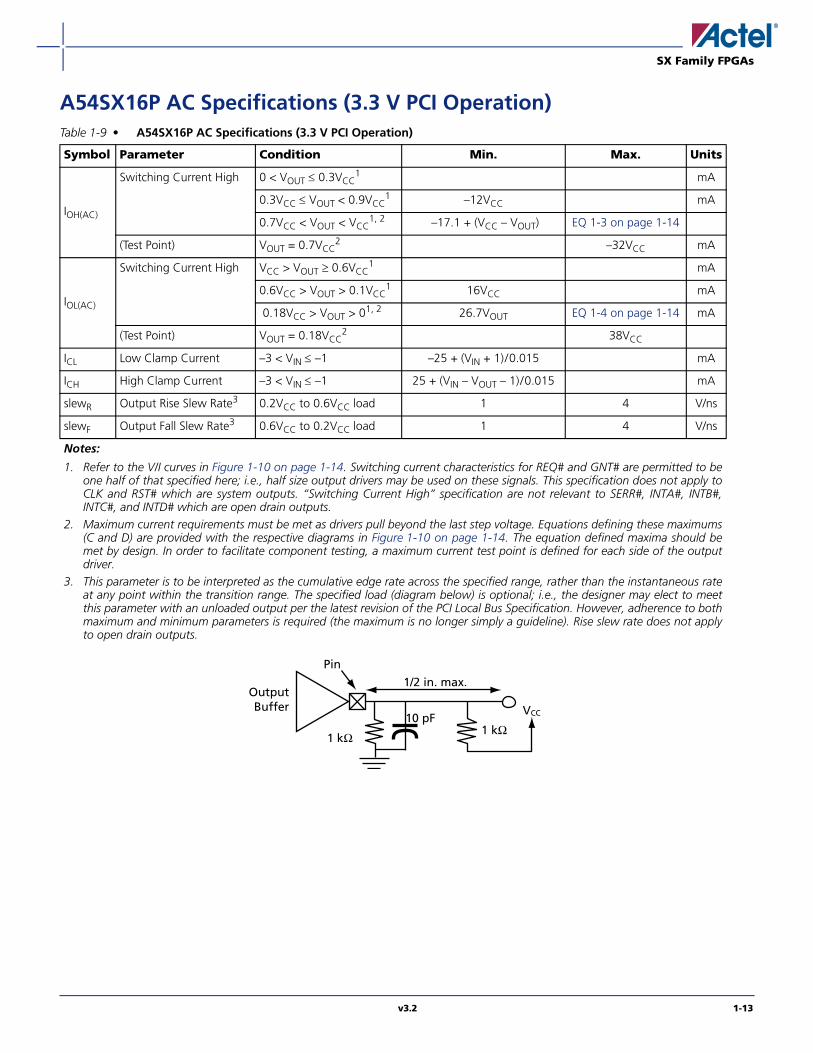
A54SX16P AC Specifications (3.3 V PCI Operation)Table 1-9 • A54SX16P AC Specifications (3.3 V PCI Operation)
Symbol Parameter Condition Min. Max. Units
IOH(AC)
Switching Current High 0 < VOUT ≤ 0.3VCC1 mA
0.3VCC ≤ VOUT < 0.9VCC1 –12VCC mA
0.7VCC < VOUT < VCC1, 2 –17.1 + (VCC – VOUT) EQ 1-3 on page 1-14
(Test Point) VOUT = 0.7VCC2 –32VCC mA
IOL(AC)
Switching Current High VCC > VOUT ≥ 0.6VCC1 mA
0.6VCC > VOUT > 0.1VCC1 16VCC mA
0.18VCC > VOUT > 01, 2 26.7VOUT EQ 1-4 on page 1-14 mA
(Test Point) VOUT = 0.18VCC2 38VCC
ICL Low Clamp Current –3 < VIN ≤ –1 –25 + (VIN + 1)/0.015 mA
ICH High Clamp Current –3 < VIN ≤ –1 25 + (VIN – VOUT – 1)/0.015 mA
slewR Output Rise Slew Rate3 0.2VCC to 0.6VCC load 1 4 V/ns
slewF Output Fall Slew Rate3 0.6VCC to 0.2VCC load 1 4 V/ns
Notes:
1. Refer to the V/I curves in Figure 1-10 on page 1-14. Switching current characteristics for REQ# and GNT# are permitted to beone half of that specified here; i.e., half size output drivers may be used on these signals. This specification does not apply toCLK and RST# which are system outputs. “Switching Current High” specification are not relevant to SERR#, INTA#, INTB#,INTC#, and INTD# which are open drain outputs.
2. Maximum current requirements must be met as drivers pull beyond the last step voltage. Equations defining these maximums(C and D) are provided with the respective diagrams in Figure 1-10 on page 1-14. The equation defined maxima should bemet by design. In order to facilitate component testing, a maximum current test point is defined for each side of the outputdriver.
3. This parameter is to be interpreted as the cumulative edge rate across the specified range, rather than the instantaneous rateat any point within the transition range. The specified load (diagram below) is optional; i.e., the designer may elect to meetthis parameter with an unloaded output per the latest revision of the PCI Local Bus Specification. However, adherence to bothmaximum and minimum parameters is required (the maximum is no longer simply a guideline). Rise slew rate does not applyto open drain outputs.
1/2 in. max.
Pin
Output Buffer VCC10 pF
1 kΩ1 kΩ
v3.2 1-13
SX Family FPGAs
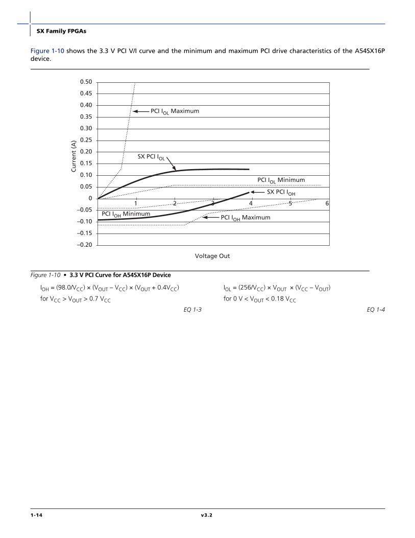
Figure 1-10 shows the 3.3 V PCI V/I curve and the minimum and maximum PCI drive characteristics of the A54SX16Pdevice.
IOH = (98.0/VCC) × (VOUT – VCC) × (VOUT + 0.4VCC)
for VCC > VOUT > 0.7 VCC
EQ 1-3
IOL = (256/VCC) × VOUT × (VCC – VOUT)
for 0 V < VOUT < 0.18 VCC
EQ 1-4
Figure 1-10 • 3.3 V PCI Curve for A54SX16P Device
PCI IOL Minimum
1 2 3 4 5 6
Voltage Out
–0.20
–0.15
–0.10
–0.05
0
0.05
0.10
0.15
0.20
0.25
0.30
0.35
0.40
0.45
0.50C
urr
ent
(A)
SX PCI IOL
SX PCI IOH
PCI IOL Maximum
PCI IOH MaximumPCI IOH Minimum
1-14 v3.2

SX Family FPGAs
Power-Up Sequencing
Power-Down Sequencing
Table 1-10 • Power-Up Sequencing
VCCA VCCR VCCI Power-Up Sequence Comments
A54SX08, A54SX16, A54SX32
3.3 V 5.0 V 3.3 V 5.0 V First3.3 V Second
No possible damage to device
3.3 V First5.0 V Second
Possible damage to device
A54SX16P
3.3 V 3.3 V 3.3 V 3.3 V Only No possible damage to device
3.3 V 5.0 V 3.3 V 5.0 V First3.3 V Second
No possible damage to device
3.3 V First5.0 V Second
Possible damage to device
3.3 V 5.0 V 5.0 V 5.0 V First3.3 V Second
No possible damage to device
3.3 V First5.0 V Second
No possible damage to device
Note: No inputs should be driven (high or low) before completion of power-up.
Table 1-11 • Power-Down Sequencing
VCCA VCCR VCCI Power-Down Sequence Comments
A54SX08, A54SX16, A54SX32
3.3 V 5.0 V 3.3 V 5.0 V First3.3 V Second
Possible damage to device
3.3 V First5.0 V Second
No possible damage to device
A54SX16P
3.3 V 3.3 V 3.3 V 3.3 V Only No possible damage to device
3.3 V 5.0 V 3.3 V 5.0 V First3.3 V Second
Possible damage to device
3.3 V First5.0 V Second
No possible damage to device
3.3 V 5.0 V 5.0 V 5.0 V First3.3 V Second
No possible damage to device
3.3 V First5.0 V Second
No possible damage to device
Note: No inputs should be driven (high or low) after the beginning of the power-down sequence.
v3.2 1-15

SX Family FPGAs
Evaluating Power in SX DevicesA critical element of system reliability is the ability ofelectronic devices to safely dissipate the heat generatedduring operation. The thermal characteristics of a circuitdepend on the device and package used, the operatingtemperature, the operating current, and the system'sability to dissipate heat.
You should complete a power evaluation early in thedesign process to help identify potential heat-relatedproblems in the system and to prevent the system fromexceeding the device’s maximum allowed junctiontemperature.
The actual power dissipated by most applications issignificantly lower than the power the package candissipate. However, a thermal analysis should beperformed for all projects. To perform a powerevaluation, follow these steps:
1. Estimate the power consumption of theapplication.
2. Calculate the maximum power allowed for thedevice and package.
3. Compare the estimated power and maximumpower values.
Estimating Power ConsumptionThe total power dissipation for the SX family is the sumof the DC power dissipation and the AC powerdissipation. Use EQ 1-5 to calculate the estimated powerconsumption of your application.
PTotal = PDC + PAC
EQ 1-5
DC Power DissipationThe power due to standby current is typically a smallcomponent of the overall power. The Standby power isshown in Table 1-12 for commercial, worst-caseconditions (70°C).
The DC power dissipation is defined in EQ 1-6.
PDC = (Istandby) × VCCA + (Istandby) × VCCR + (Istandby) × VCCI + xVOL × IOL + y(VCCI – VOH) × VOH
EQ 1-6
AC Power DissipationThe power dissipation of the SX Family is usuallydominated by the dynamic power dissipation. Dynamicpower dissipation is a function of frequency, equivalentcapacitance, and power supply voltage. The AC powerdissipation is defined in EQ 1-7 and EQ 1-8.
PAC = PModule + PRCLKA Net + PRCLKB Net + PHCLK Net +POutput Buffer + PInput Buffer
EQ 1-7
PAC = VCCA2 × [(m × CEQM × fm)Module +
(n × CEQI × fn)Input Buffer+ (p × (CEQO + CL) × fp)Output Buffer + (0.5 × (q1 × CEQCR × fq1) + (r1 × fq1))RCLKA + (0.5 × (q2 × CEQCR × fq2)+ (r2 × fq2))RCLKB + (0.5 × (s1 × CEQHV × fs1) + (CEQHF × fs1))HCLK]
EQ 1-8
Definition of Terms Used in Formulam = Number of logic modules switching at fm
n = Number of input buffers switching at fn
p = Number of output buffers switching at fp
q1 = Number of clock loads on the first routed arrayclock
q2 = Number of clock loads on the second routed arrayclock
x = Number of I/Os at logic lowy = Number of I/Os at logic highr1 = Fixed capacitance due to first routed array clockr2 = Fixed capacitance due to second routed array
clocks1 = Number of clock loads on the dedicated array
clockCEQM = Equivalent capacitance of logic modules in pFCEQI = Equivalent capacitance of input buffers in pFCEQO = Equivalent capacitance of output buffers in pFCEQCR = Equivalent capacitance of routed array clock in pFCEQHV = Variable capacitance of dedicated array clockCEQHF = Fixed capacitance of dedicated array clockCL = Output lead capacitance in pFfm = Average logic module switching rate in MHzfn = Average input buffer switching rate in MHzfp = Average output buffer switching rate in MHzfq1 = Average first routed array clock rate in MHzfq2 = Average second routed array clock rate in MHzfs1 = Average dedicated array clock rate in MHz
Table 1-12 • Standby Power
ICC VCC Power
4 mA 3.6 V 14.4 mW
1-16 v3.2
SX Family FPGAs
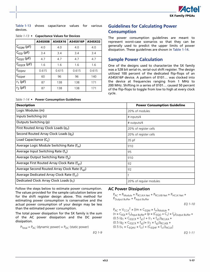
Table 1-13 shows capacitance values for variousdevices.
Guidelines for Calculating Power ConsumptionThe power consumption guidelines are meant torepresent worst-case scenarios so that they can begenerally used to predict the upper limits of powerdissipation. These guidelines are shown in Table 1-14.
Sample Power Calculation One of the designs used to characterize the SX familywas a 528 bit serial-in, serial-out shift register. The designutilized 100 percent of the dedicated flip-flops of anA54SX16P device. A pattern of 0101… was clocked intothe device at frequencies ranging from 1 MHz to200 MHz. Shifting in a series of 0101… caused 50 percentof the flip-flops to toggle from low to high at every clockcycle.
Follow the steps below to estimate power consumption.The values provided for the sample calculation below arefor the shift register design above. This method forestimating power consumption is conservative and theactual power consumption of your design may be lessthan the estimated power consumption.
The total power dissipation for the SX family is the sumof the AC power dissipation and the DC powerdissipation.
PTotal = PAC (dynamic power) + PDC (static power)
EQ 1-9
AC Power DissipationPAC = PModule + PRCLKA Net + PRCLKB Net + PHCLK Net +POutput Buffer + PInput Buffer
EQ 1-10
PAC = VCCA2 × [(m × CEQM × fm)Module +
(n × CEQI × fn)Input Buffer+ (p × (CEQO + CL) × fp)Output Buffer +(0.5 (q1 × CEQCR × fq1) + (r1 × fq1))RCLKA + (0.5 (q2 × CEQCR × fq2)+ (r2 × fq2))RCLKB + (0.5 (s1 × CEQHV × fs1) + (CEQHF × fs1))HCLK]
EQ 1-11
Table 1-13 • Capacitance Values for Devices
A54SX08 A54SX16 A54SX16P A54SX32
CEQM (pF) 4.0 4.0 4.0 4.0
CEQI (pF) 3.4 3.4 3.4 3.4
CEQO (pF) 4.7 4.7 4.7 4.7
CEQCR (pF) 1.6 1.6 1.6 1.6
CEQHV 0.615 0.615 0.615 0.615
CEQHF 60 96 96 140
r1 (pF) 87 138 138 171
r2 (pF) 87 138 138 171
Table 1-14 • Power Consumption Guidelines
Description Power Consumption Guideline
Logic Modules (m) 20% of modules
Inputs Switching (n) # inputs/4
Outputs Switching (p) # outputs/4
First Routed Array Clock Loads (q1) 20% of register cells
Second Routed Array Clock Loads (q2) 20% of register cells
Load Capacitance (CL) 35 pF
Average Logic Module Switching Rate (fm) f/10
Average Input Switching Rate (fn) f/5
Average Output Switching Rate (fp) f/10
Average First Routed Array Clock Rate (fq1) f/2
Average Second Routed Array Clock Rate (fq2) f/2
Average Dedicated Array Clock Rate (fs1) f
Dedicated Clock Array Clock Loads (s1) 20% of regular modules
v3.2 1-17
SX Family FPGAs
Step 3: Calculate DC Power DissipationDC Power Dissipation
PDC = (Istandby) × VCCA + (Istandby) × VCCR + (Istandby) × VCCI + X × VOL × IOL + Y(VCCI – VOH) × VOH
EQ 1-12
For a rough estimate of DC Power Dissipation, only usePDC = (Istandby) × VCCA. The rest of the formula provides avery small number that can be considered negligible.
PDC = (Istandby) × VCCA
PDC = .55 mA × 3.3 V
PDC = 0.001815 W
Step 4: Calculate Total Power ConsumptionPTotal = PAC + PDC
PTotal = 1.461 + 0.001815
PTotal = 1.4628 W
Step 5: Compare Estimated Power Consumption against Characterized Power ConsumptionThe estimated total power consumption for this design is1.46 W. The characterized power consumption for thisdesign at 200 MHz is 1.0164 W.
Step 1: Define Terms Used in Formula VCCA 3.3
Module
Number of logic modules switching at fm (Used 50%)
m 264
Average logic modules switching rate fm (MHz) (Guidelines: f/10)
fm 20
Module capacitance CEQM (pF) CEQM 4.0
Input Buffer
Number of input buffers switching at fn n 1
Average input switching rate fn (MHz)(Guidelines: f/5)
fn 40
Input buffer capacitance CEQI (pF) CEQI 3.4
Output Buffer
Number of output buffers switching at fp p 1
Average output buffers switching rate fp(MHz) (Guidelines: f/10)
fp 20
Output buffers buffer capacitance CEQO (pF)
CEQO 4.7
Output Load capacitance CL (pF) CL 35
RCLKA
Number of Clock loads q1 q1 528
Capacitance of routed array clock (pF) CEQCR 1.6
Average clock rate (MHz) fq1 200
Fixed capacitance (pF) r1 138
RCLKB
Number of Clock loads q2 q2 0
Capacitance of routed array clock (pF) CEQCR 1.6
Average clock rate (MHz) fq2 0
Fixed capacitance (pF) r2 138
HCLK
Number of Clock loads s1 0
Variable capacitance of dedicated array clock (pF)
CEQHV 0.615
Fixed capacitance of dedicated array clock (pF)
CEQHF 96
Average clock rate (MHz) fs1 0
Step 2: Calculate Dynamic Power ConsumptionVCCA × VCCA 10.89
m × fm × CEQM 0.02112
n × fn × CEQI 0.000136
p × fp × (CEQO+CL) 0.000794
0.5 (q1 × CEQCR × fq1) + (r1 × fq1) 0.11208
0.5(q2 × CEQCR × fq2) + (r2 × fq2) 0
0.5 (s1 × CEQHV × fs1) + (CEQHF × fs1) 0
PAC = 1.461 W
1-18 v3.2

SX Family FPGAs
Figure 1-11 shows the characterized power dissipation numbers for the shift register design using frequencies rangingfrom 1 MHz to 200 MHz.
Junction Temperature (TJ)The temperature that you select in Designer Seriessoftware is the junction temperature, not ambienttemperature. This is an important distinction because theheat generated from dynamic power consumption isusually hotter than the ambient temperature. Use theequation below to calculate junction temperature.
Junction Temperature = ΔT + Ta
EQ 1-13
Where:
Ta = Ambient Temperature
ΔT = Temperature gradient between junction (silicon)and ambient
ΔT = θja × P
P = Power calculated from Estimating PowerConsumption section
θja = Junction to ambient of package. θja numbers arelocated in the "Package Thermal Characteristics"section.
Package Thermal CharacteristicsThe device junction to case thermal characteristic is θjc,and the junction to ambient air characteristic is θja. Thethermal characteristics for θja are shown with twodifferent air flow rates.
The maximum junction temperature is 150 °C.
A sample calculation of the absolute maximum powerdissipation allowed for a TQFP 176-pin package atcommercial temperature and still air is as follows:
EQ 1-14
Figure 1-11 • Power Dissipation
0
200
400
600
800
1000
1200
Frequency MHz
Pow
er D
issi
pat
ion
mW
200 40 60 80 100 120 140 160 180 200
Maximum Power Allowed Max. junction temp. (°C) – Max. ambient temp. (°C)θja (°C/W)
------------------------------------------------------------------------------------------------------------------------------------ 150°C – 70°C28°C/W
----------------------------------- 2.86 W= = =
v3.2 1-19

SX Family FPGAs
Table 1-15 • Package Thermal Characteristics
Package Type Pin Count θjc
θjaStill Air
θja300 ft/min. Units
Plastic Leaded Chip Carrier (PLCC) 84 12 32 22 °C/W
Thin Quad Flat Pack (TQFP) 144 11 32 24 °C/W
Thin Quad Flat Pack (TQFP) 176 11 28 21 °C/W
Very Thin Quad Flatpack (VQFP) 100 10 38 32 °C/W
Plastic Quad Flat Pack (PQFP) without Heat Spreader 208 8 30 23 °C/W
Plastic Quad Flat Pack (PQFP) with Heat Spreader 208 3.8 20 17 °C/W
Plastic Ball Grid Array (PBGA) 272 3 20 14.5 °C/W
Plastic Ball Grid Array (PBGA) 313 3 23 17 °C/W
Plastic Ball Grid Array (PBGA) 329 3 18 13.5 °C/W
Fine Pitch Ball Grid Array (FBGA) 144 3.8 38.8 26.7 °C/W
Note: SX08 does not have a heat spreader.
Table 1-16 • Temperature and Voltage Derating Factors*
VCCA
Junction Temperature
–55 –40 0 25 70 85 125
3.0 0.75 0.78 0.87 0.89 1.00 1.04 1.16
3.3 0.70 0.73 0.82 0.83 0.93 0.97 1.08
3.6 0.66 0.69 0.77 0.78 0.87 0.92 1.02
Note: *Normalized to worst-case commercial, TJ = 70°C, VCCA = 3.0 V
1-20 v3.2

SX Family FPGAs
SX Timing Model
Hardwired ClockExternal Setup = tINY + tIRD1 + tSUD – tHCKH
= 1.5 + 0.3 + 0.5 – 1.0 = 1.3 ns
EQ 1-15
Clock-to-Out (Pin-to-Pin)
= tHCKH + tRCO + tRD1 + tDHL
= 1.0 + 0.8 + 0.3 + 1.6 = 3.7 ns
EQ 1-16
Routed ClockExternal Setup = tINY + tIRD1 + tSUD – tRCKH
= 1.5 + 0.3 + 0.5 – 1.5 = 0.8 ns
EQ 1-17
Clock-to-Out (Pin-to-Pin)
= tRCKH + tRCO + tRD1 + tDHL
= 1.52+ 0.8 + 0.3 + 1.6 = 4.2 ns
EQ 1-18
Note: Values shown for A54SX08-3, worst-case commercial conditions.Figure 1-12 • SX Timing Model
D Q
Routed Clock
FMAX = 250 MHz
tRCKH = 1.5 ns (100% Load)
tINY = 1.5 ns
Output DelaysInput Delays
I/O Module Combinatorial Cell
Register Cell
I/O Module
I/O Module
Hardwired Clock
D Q
PredictedRoutingDelays
tIRD2 = 0.6 ns
tPD = 0.6 nstRD1 = 0.3 nstRD4 = 1.0 nstRD8 = 1.9 ns
tDLH = 1.6 ns
tDHL = 1.6 ns
FHMAX = 320 MHz
tHCKH = 1.0 ns
tRCO = 0.8 ns
tRD1 = 0.3 nstENZH = 2.3 ns
Internal Delays
tRD1 = 0.3 ns
tSUD = 0.5 nstHD = 0.0 ns
Register Cell
tRCO = 0.8 ns
v3.2 1-21
SX Family FPGAs
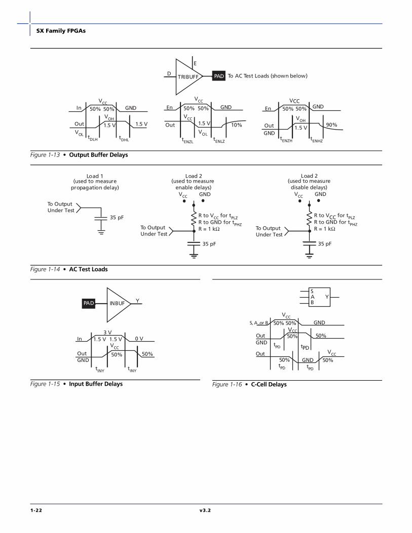
Figure 1-13 • Output Buffer Delays
Figure 1-14 • AC Test Loads
To AC Test Loads (shown below)PADD
E
TRIBUFF
In 50%
Out
VOL
1.5 V
50%
1.5 V
En 50%
OutVOL
1.5 V
50%
10%
En 50%
OutGND
1.5 V
50%
90%
tDLH tDHL tENZLtENLZ
tENZH tENHZ
VOH VOH
GNDVCC
GND
VCC
VCCVCCGND
Load 2(used to measure
disable delays)VCC GND
35 pF
R to VCC for tPLZ R to GND for tPHZ R = 1 kΩ
Load 1(used to measure
propagation delay)
Load 2(used to measure
enable delays)
35 pF
To Output Under Test
VCC GND
35 pF
R to VCC for tPLZ R to GND for tPHZ R = 1 kΩTo Output
Under TestTo Output Under Test
Figure 1-15 • Input Buffer Delays
PAD YINBUF
In3 V
0 V1.5 V
OutGND
VCC
50%
tINY
1.5 V
50%
tINY
Figure 1-16 • C-Cell Delays
SAB
Y
S, A ,or B
Out
50%
tPD
Out
50%
50% 50%
50% 50%tPD
tPDtPD
VCCGND
GND
VCC
GND
VCC
1-22 v3.2

SX Family FPGAs
Register Cell Timing Characteristics
Timing CharacteristicsTiming characteristics for SX devices fall into threecategories: family-dependent, device-dependent, anddesign-dependent. The input and output buffercharacteristics are common to all SX family members.Internal routing delays are device-dependent. Designdependency means actual delays are not determineduntil after placement and routing of the user’s design iscomplete. Delay values may then be determined by usingthe DirectTime Analyzer utility or performing simulationwith post-layout delays.
Critical Nets and Typical NetsPropagation delays are expressed only for typical nets,which are used for initial design performance evaluation.Critical net delays can then be applied to the most time-critical paths. Critical nets are determined by netproperty assignment prior to placement and routing. Upto 6% of the nets in a design may be designated ascritical, while 90% of the nets in a design are typical.
Long TracksSome nets in the design use long tracks. Long tracks arespecial routing resources that span multiple rows,columns, or modules. Long tracks employ three andsometimes five antifuse connections. This increasescapacitance and resistance, resulting in longer net delaysfor macros connected to long tracks. Typically up to 6percent of nets in a fully utilized device require longtracks. Long tracks contribute approximately 4 ns to 8.4ns delay. This additional delay is represented statisticallyin higher fanout (FO = 24) routing delays in thedatasheet specifications section.
Timing DeratingSX devices are manufactured in a CMOS process.Therefore, device performance varies according totemperature, voltage, and process variations. Minimumtiming parameters reflect maximum operating voltage,minimum operating temperature, and best-caseprocessing. Maximum timing parameters reflectminimum operating voltage, maximum operatingtemperature, and worst-case processing.
Figure 1-17 • Flip-Flops
tCLR
(positive edge triggered)
D
CLK
CLR
PRESET Q
D
CLK
Q
CLR
PRESET
tHPWH'
tWASYN
tHD
tSUD tHP
tHPWL'tRCO
tPRESET
RPWL
RPWH
v3.2 1-23
SX Family FPGAs
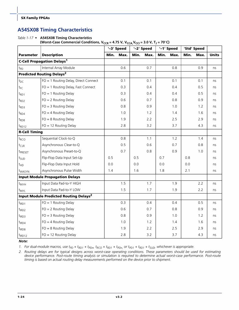
A54SX08 Timing Characteristics
Table 1-17 • A54SX08 Timing Characteristics (Worst-Case Commercial Conditions, VCCR = 4.75 V, VCCA,VCCI = 3.0 V, TJ = 70°C)
Parameter Description
'–3' Speed '–2' Speed '–1' Speed 'Std' Speed
Min. Max. Min. Max. Min. Max. Min. Max. Units
C-Cell Propagation Delays1
tPD Internal Array Module 0.6 0.7 0.8 0.9 ns
Predicted Routing Delays2
tDC FO = 1 Routing Delay, Direct Connect 0.1 0.1 0.1 0.1 ns
tFC FO = 1 Routing Delay, Fast Connect 0.3 0.4 0.4 0.5 ns
tRD1 FO = 1 Routing Delay 0.3 0.4 0.4 0.5 ns
tRD2 FO = 2 Routing Delay 0.6 0.7 0.8 0.9 ns
tRD3 FO = 3 Routing Delay 0.8 0.9 1.0 1.2 ns
tRD4 FO = 4 Routing Delay 1.0 1.2 1.4 1.6 ns
tRD8 FO = 8 Routing Delay 1.9 2.2 2.5 2.9 ns
tRD12 FO = 12 Routing Delay 2.8 3.2 3.7 4.3 ns
R-Cell Timing
tRCO Sequential Clock-to-Q 0.8 1.1 1.2 1.4 ns
tCLR Asynchronous Clear-to-Q 0.5 0.6 0.7 0.8 ns
tPRESET Asynchronous Preset-to-Q 0.7 0.8 0.9 1.0 ns
tSUD Flip-Flop Data Input Set-Up 0.5 0.5 0.7 0.8 ns
tHD Flip-Flop Data Input Hold 0.0 0.0 0.0 0.0 ns
tWASYN Asynchronous Pulse Width 1.4 1.6 1.8 2.1 ns
Input Module Propagation Delays
tINYH Input Data Pad-to-Y HIGH 1.5 1.7 1.9 2.2 ns
tINYL Input Data Pad-to-Y LOW 1.5 1.7 1.9 2.2 ns
Input Module Predicted Routing Delays2
tIRD1 FO = 1 Routing Delay 0.3 0.4 0.4 0.5 ns
tIRD2 FO = 2 Routing Delay 0.6 0.7 0.8 0.9 ns
tIRD3 FO = 3 Routing Delay 0.8 0.9 1.0 1.2 ns
tIRD4 FO = 4 Routing Delay 1.0 1.2 1.4 1.6 ns
tIRD8 FO = 8 Routing Delay 1.9 2.2 2.5 2.9 ns
tIRD12 FO = 12 Routing Delay 2.8 3.2 3.7 4.3 ns
Note:
1. For dual-module macros, use tPD + tRD1 + tPDn, tRCO + tRD1 + tPDn, or tPD1 + tRD1 + tSUD, whichever is appropriate.2. Routing delays are for typical designs across worst-case operating conditions. These parameters should be used for estimating
device performance. Post-route timing analysis or simulation is required to determine actual worst-case performance. Post-routetiming is based on actual routing delay measurements performed on the device prior to shipment.
1-24 v3.2

SX Family FPGAs
Dedicated (Hardwired) Array Clock Network
tHCKH Input LOW to HIGH (pad to R-Cell input) 1.0 1.1 1.3 1.5 ns
tHCKL Input HIGH to LOW (pad to R-Cell input) 1.0 1.2 1.4 1.6 ns
tHPWH Minimum Pulse Width HIGH 1.4 1.6 1.8 2.1 ns
tHPWL Minimum Pulse Width LOW 1.4 1.6 1.8 2.1 ns
tHCKSW Maximum Skew 0.1 0.2 0.2 0.2 ns
tHP Minimum Period 2.7 3.1 3.6 4.2 ns
fHMAX Maximum Frequency 350 320 280 240 MHz
Routed Array Clock Networks
tRCKH Input LOW to HIGH (light load)(pad to R-Cell input)
1.3 1.5 1.7 2.0 ns
tRCKL Input HIGH to LOW (light load)(pad to R-Cell Input)
1.4 1.6 1.8 2.1 ns
tRCKH Input LOW to HIGH (50% load)(pad to R-Cell input)
1.4 1.7 1.9 2.2 ns
tRCKL Input HIGH to LOW (50% load)(pad to R-Cell input)
1.5 1.7 2.0 2.3 ns
tRCKH Input LOW to HIGH (100% load)(pad to R-Cell input)
1.5 1.7 1.9 2.2 ns
tRCKL Input HIGH to LOW (100% load)(pad to R-Cell input)
1.5 1.8 2.0 2.3 ns
tRPWH Min. Pulse Width HIGH 2.1 2.4 2.7 3.2 ns
tRPWL Min. Pulse Width LOW 2.1 2.4 2.7 3.2 ns
tRCKSW Maximum Skew (light load) 0.1 0.2 0.2 0.2 ns
tRCKSW Maximum Skew (50% load) 0.3 0.3 0.4 0.4 ns
tRCKSW Maximum Skew (100% load) 0.3 0.3 0.4 0.4 ns
TTL Output Module Timing1
tDLH Data-to-Pad LOW to HIGH 1.6 1.9 2.1 2.5 ns
tDHL Data-to-Pad HIGH to LOW 1.6 1.9 2.1 2.5 ns
tENZL Enable-to-Pad, Z to L 2.1 2.4 2.8 3.2 ns
tENZH Enable-to-Pad, Z to H 2.3 2.7 3.1 3.6 ns
tENLZ Enable-to-Pad, L to Z 1.4 1.7 1.9 2.2 ns
Table 1-17 • A54SX08 Timing Characteristics (Continued)(Worst-Case Commercial Conditions, VCCR = 4.75 V, VCCA,VCCI = 3.0 V, TJ = 70°C)
Parameter Description
'–3' Speed '–2' Speed '–1' Speed 'Std' Speed
Min. Max. Min. Max. Min. Max. Min. Max. Units
Note:
1. For dual-module macros, use tPD + tRD1 + tPDn, tRCO + tRD1 + tPDn, or tPD1 + tRD1 + tSUD, whichever is appropriate.2. Routing delays are for typical designs across worst-case operating conditions. These parameters should be used for estimating
device performance. Post-route timing analysis or simulation is required to determine actual worst-case performance. Post-routetiming is based on actual routing delay measurements performed on the device prior to shipment.
v3.2 1-25

SX Family FPGAs
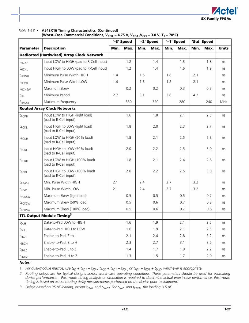
A54SX16 Timing Characteristics
Table 1-18 • A54SX16 Timing Characteristics (Worst-Case Commercial Conditions, VCCR = 4.75 V, VCCA ,VCCI = 3.0 V, TJ = 70°C)
Parameter Description
'–3' Speed '–2' Speed '–1' Speed 'Std' Speed
Min. Max. Min. Max. Min. Max. Min. Max. Units
C-Cell Propagation Delays1
tPD Internal Array Module 0.6 0.7 0.8 0.9 ns
Predicted Routing Delays2
tDC FO = 1 Routing Delay, Direct Connect 0.1 0.1 0.1 0.1 ns
tFC FO = 1 Routing Delay, Fast Connect 0.3 0.4 0.4 0.5 ns
tRD1 FO = 1 Routing Delay 0.3 0.4 0.4 0.5 ns
tRD2 FO = 2 Routing Delay 0.6 0.7 0.8 0.9 ns
tRD3 FO = 3 Routing Delay 0.8 0.9 1.0 1.2 ns
tRD4 FO = 4 Routing Delay 1.0 1.2 1.4 1.6 ns
tRD8 FO = 8 Routing Delay 1.9 2.2 2.5 2.9 ns
tRD12 FO = 12 Routing Delay 2.8 3.2 3.7 4.3 ns
R-Cell Timing
tRCO Sequential Clock-to-Q 0.8 1.1 1.2 1.4 ns
tCLR Asynchronous Clear-to-Q 0.5 0.6 0.7 0.8 ns
tPRESET Asynchronous Preset-to-Q 0.7 0.8 0.9 1.0 ns
tSUD Flip-Flop Data Input Set-Up 0.5 0.5 0.7 0.8 ns
tHD Flip-Flop Data Input Hold 0.0 0.0 0.0 0.0 ns
tWASYN Asynchronous Pulse Width 1.4 1.6 1.8 2.1 ns
Input Module Propagation Delays
tINYH Input Data Pad-to-Y HIGH 1.5 1.7 1.9 2.2 ns
tINYL Input Data Pad-to-Y LOW 1.5 1.7 1.9 2.2 ns
Predicted Input Routing Delays2
tIRD1 FO = 1 Routing Delay 0.3 0.4 0.4 0.5 ns
tIRD2 FO = 2 Routing Delay 0.6 0.7 0.8 0.9 ns
tIRD3 FO = 3 Routing Delay 0.8 0.9 1.0 1.2 ns
tIRD4 FO = 4 Routing Delay 1.0 1.2 1.4 1.6 ns
tIRD8 FO = 8 Routing Delay 1.9 2.2 2.5 2.9 ns
tIRD12 FO = 12 Routing Delay 2.8 3.2 3.7 4.3 ns
Notes:
1. For dual-module macros, use tPD + tRD1 + tPDn, tRCO + tRD1 + tPDn, or tPD1 + tRD1 + tSUD, whichever is appropriate.2. Routing delays are for typical designs across worst-case operating conditions. These parameters should be used for estimating
device performance. Post-route timing analysis or simulation is required to determine actual worst-case performance. Post-routetiming is based on actual routing delay measurements performed on the device prior to shipment.
3. Delays based on 35 pF loading, except tENZL and tENZH. For tENZL and tENZH, the loading is 5 pF.
1-26 v3.2
SX Family FPGAs
Dedicated (Hardwired) Array Clock Network
tHCKH Input LOW to HIGH (pad to R-Cell input) 1.2 1.4 1.5 1.8 ns
tHCKL Input HIGH to LOW (pad to R-Cell input) 1.2 1.4 1.6 1.9 ns
tHPWH Minimum Pulse Width HIGH 1.4 1.6 1.8 2.1 ns
tHPWL Minimum Pulse Width LOW 1.4 1.6 1.8 2.1 ns
tHCKSW Maximum Skew 0.2 0.2 0.3 0.3 ns
tHP Minimum Period 2.7 3.1 3.6 4.2 ns
fHMAX Maximum Frequency 350 320 280 240 MHz
Routed Array Clock Networks
tRCKH Input LOW to HIGH (light load)(pad to R-Cell input)
1.6 1.8 2.1 2.5 ns
tRCKL Input HIGH to LOW (light load)(pad to R-Cell input)
1.8 2.0 2.3 2.7 ns
tRCKH Input LOW to HIGH (50% load)(pad to R-Cell input)
1.8 2.1 2.5 2.8 ns
tRCKL Input HIGH to LOW (50% load)(pad to R-Cell input)
2.0 2.2 2.5 3.0 ns
tRCKH Input LOW to HIGH (100% load)(pad to R-Cell input)
1.8 2.1 2.4 2.8 ns
tRCKL Input HIGH to LOW (100% load)(pad to R-Cell input)
2.0 2.2 2.5 3.0 ns
tRPWH Min. Pulse Width HIGH 2.1 2.4 2.7 3.2 ns
tRPWL Min. Pulse Width LOW 2.1 2.4 2.7 3.2 ns
tRCKSW Maximum Skew (light load) 0.5 0.5 0.5 0.7 ns
tRCKSW Maximum Skew (50% load) 0.5 0.6 0.7 0.8 ns
tRCKSW Maximum Skew (100% load) 0.5 0.6 0.7 0.8 ns
TTL Output Module Timing3
tDLH Data-to-Pad LOW to HIGH 1.6 1.9 2.1 2.5 ns
tDHL Data-to-Pad HIGH to LOW 1.6 1.9 2.1 2.5 ns
tENZL Enable-to-Pad, Z to L 2.1 2.4 2.8 3.2 ns
tENZH Enable-to-Pad, Z to H 2.3 2.7 3.1 3.6 ns
tENLZ Enable-to-Pad, L to Z 1.4 1.7 1.9 2.2 ns
tENHZ Enable-to-Pad, H to Z 1.3 1.5 1.7 2.0 ns
Table 1-18 • A54SX16 Timing Characteristics (Continued)(Worst-Case Commercial Conditions, VCCR = 4.75 V, VCCA ,VCCI = 3.0 V, TJ = 70°C)
Parameter Description
'–3' Speed '–2' Speed '–1' Speed 'Std' Speed
Min. Max. Min. Max. Min. Max. Min. Max. Units
Notes:
1. For dual-module macros, use tPD + tRD1 + tPDn, tRCO + tRD1 + tPDn, or tPD1 + tRD1 + tSUD, whichever is appropriate.2. Routing delays are for typical designs across worst-case operating conditions. These parameters should be used for estimating
device performance. Post-route timing analysis or simulation is required to determine actual worst-case performance. Post-routetiming is based on actual routing delay measurements performed on the device prior to shipment.
3. Delays based on 35 pF loading, except tENZL and tENZH. For tENZL and tENZH, the loading is 5 pF.
v3.2 1-27
SX Family FPGAs
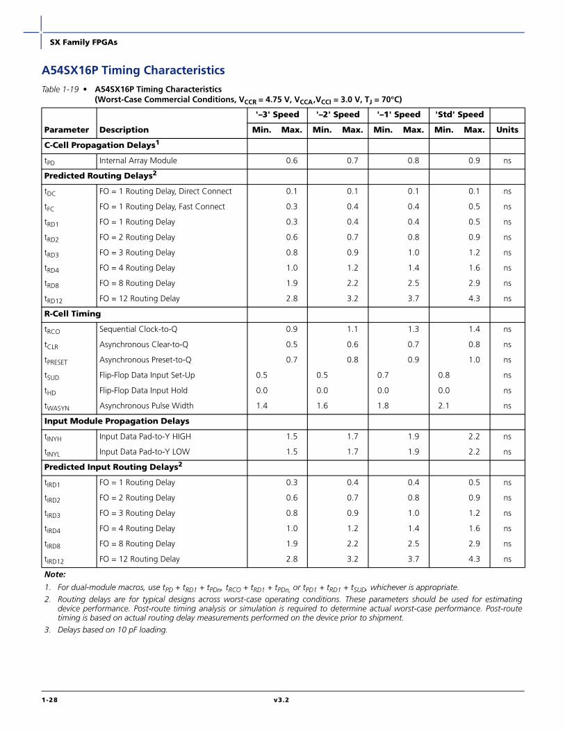
A54SX16P Timing Characteristics
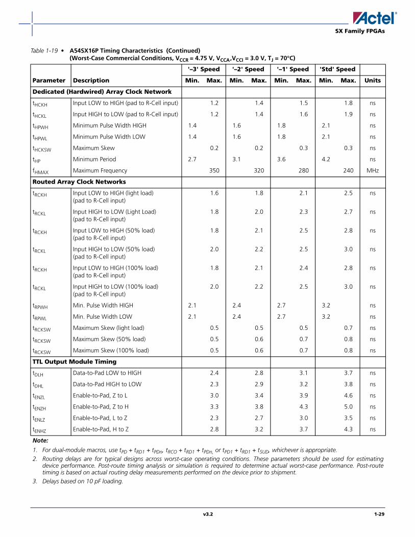
Table 1-19 • A54SX16P Timing Characteristics (Worst-Case Commercial Conditions, VCCR = 4.75 V, VCCA,VCCI = 3.0 V, TJ = 70°C)
Parameter Description
'–3' Speed '–2' Speed '–1' Speed 'Std' Speed
Min. Max. Min. Max. Min. Max. Min. Max. Units
C-Cell Propagation Delays1
tPD Internal Array Module 0.6 0.7 0.8 0.9 ns
Predicted Routing Delays2
tDC FO = 1 Routing Delay, Direct Connect 0.1 0.1 0.1 0.1 ns
tFC FO = 1 Routing Delay, Fast Connect 0.3 0.4 0.4 0.5 ns
tRD1 FO = 1 Routing Delay 0.3 0.4 0.4 0.5 ns
tRD2 FO = 2 Routing Delay 0.6 0.7 0.8 0.9 ns
tRD3 FO = 3 Routing Delay 0.8 0.9 1.0 1.2 ns
tRD4 FO = 4 Routing Delay 1.0 1.2 1.4 1.6 ns
tRD8 FO = 8 Routing Delay 1.9 2.2 2.5 2.9 ns
tRD12 FO = 12 Routing Delay 2.8 3.2 3.7 4.3 ns
R-Cell Timing
tRCO Sequential Clock-to-Q 0.9 1.1 1.3 1.4 ns
tCLR Asynchronous Clear-to-Q 0.5 0.6 0.7 0.8 ns
tPRESET Asynchronous Preset-to-Q 0.7 0.8 0.9 1.0 ns
tSUD Flip-Flop Data Input Set-Up 0.5 0.5 0.7 0.8 ns
tHD Flip-Flop Data Input Hold 0.0 0.0 0.0 0.0 ns
tWASYN Asynchronous Pulse Width 1.4 1.6 1.8 2.1 ns
Input Module Propagation Delays
tINYH Input Data Pad-to-Y HIGH 1.5 1.7 1.9 2.2 ns
tINYL Input Data Pad-to-Y LOW 1.5 1.7 1.9 2.2 ns
Predicted Input Routing Delays2
tIRD1 FO = 1 Routing Delay 0.3 0.4 0.4 0.5 ns
tIRD2 FO = 2 Routing Delay 0.6 0.7 0.8 0.9 ns
tIRD3 FO = 3 Routing Delay 0.8 0.9 1.0 1.2 ns
tIRD4 FO = 4 Routing Delay 1.0 1.2 1.4 1.6 ns
tIRD8 FO = 8 Routing Delay 1.9 2.2 2.5 2.9 ns
tIRD12 FO = 12 Routing Delay 2.8 3.2 3.7 4.3 ns
Note:
1. For dual-module macros, use tPD + tRD1 + tPDn, tRCO + tRD1 + tPDn, or tPD1 + tRD1 + tSUD, whichever is appropriate.2. Routing delays are for typical designs across worst-case operating conditions. These parameters should be used for estimating
device performance. Post-route timing analysis or simulation is required to determine actual worst-case performance. Post-routetiming is based on actual routing delay measurements performed on the device prior to shipment.
3. Delays based on 10 pF loading.
1-28 v3.2
SX Family FPGAs
Dedicated (Hardwired) Array Clock Network
tHCKH Input LOW to HIGH (pad to R-Cell input) 1.2 1.4 1.5 1.8 ns
tHCKL Input HIGH to LOW (pad to R-Cell input) 1.2 1.4 1.6 1.9 ns
tHPWH Minimum Pulse Width HIGH 1.4 1.6 1.8 2.1 ns
tHPWL Minimum Pulse Width LOW 1.4 1.6 1.8 2.1 ns
tHCKSW Maximum Skew 0.2 0.2 0.3 0.3 ns
tHP Minimum Period 2.7 3.1 3.6 4.2 ns
fHMAX Maximum Frequency 350 320 280 240 MHz
Routed Array Clock Networks
tRCKH Input LOW to HIGH (light load)(pad to R-Cell input)
1.6 1.8 2.1 2.5 ns
tRCKL Input HIGH to LOW (Light Load)(pad to R-Cell input)
1.8 2.0 2.3 2.7 ns
tRCKH Input LOW to HIGH (50% load)(pad to R-Cell input)
1.8 2.1 2.5 2.8 ns
tRCKL Input HIGH to LOW (50% load)(pad to R-Cell input)
2.0 2.2 2.5 3.0 ns
tRCKH Input LOW to HIGH (100% load)(pad to R-Cell input)
1.8 2.1 2.4 2.8 ns
tRCKL Input HIGH to LOW (100% load)(pad to R-Cell input)
2.0 2.2 2.5 3.0 ns
tRPWH Min. Pulse Width HIGH 2.1 2.4 2.7 3.2 ns
tRPWL Min. Pulse Width LOW 2.1 2.4 2.7 3.2 ns
tRCKSW Maximum Skew (light load) 0.5 0.5 0.5 0.7 ns
tRCKSW Maximum Skew (50% load) 0.5 0.6 0.7 0.8 ns
tRCKSW Maximum Skew (100% load) 0.5 0.6 0.7 0.8 ns
TTL Output Module Timing
tDLH Data-to-Pad LOW to HIGH 2.4 2.8 3.1 3.7 ns
tDHL Data-to-Pad HIGH to LOW 2.3 2.9 3.2 3.8 ns
tENZL Enable-to-Pad, Z to L 3.0 3.4 3.9 4.6 ns
tENZH Enable-to-Pad, Z to H 3.3 3.8 4.3 5.0 ns
tENLZ Enable-to-Pad, L to Z 2.3 2.7 3.0 3.5 ns
tENHZ Enable-to-Pad, H to Z 2.8 3.2 3.7 4.3 ns
Table 1-19 • A54SX16P Timing Characteristics (Continued)(Worst-Case Commercial Conditions, VCCR = 4.75 V, VCCA,VCCI = 3.0 V, TJ = 70°C)
Parameter Description
'–3' Speed '–2' Speed '–1' Speed 'Std' Speed
Min. Max. Min. Max. Min. Max. Min. Max. Units
Note:
1. For dual-module macros, use tPD + tRD1 + tPDn, tRCO + tRD1 + tPDn, or tPD1 + tRD1 + tSUD, whichever is appropriate.2. Routing delays are for typical designs across worst-case operating conditions. These parameters should be used for estimating
device performance. Post-route timing analysis or simulation is required to determine actual worst-case performance. Post-routetiming is based on actual routing delay measurements performed on the device prior to shipment.
3. Delays based on 10 pF loading.
v3.2 1-29

SX Family FPGAs
TTL/PCI Output Module Timing
tDLH Data-to-Pad LOW to HIGH 1.5 1.7 2.0 2.3 ns
tDHL Data-to-Pad HIGH to LOW 1.9 2.2 2.4 2.9 ns
tENZL Enable-to-Pad, Z to L 2.3 2.6 3.0 3.5 ns
tENZH Enable-to-Pad, Z to H 1.5 1.7 1.9 2.3 ns
tENLZ Enable-to-Pad, L to Z 2.7 3.1 3.5 4.1 ns
tENHZ Enable-to-Pad, H to Z 2.9 3.3 3.7 4.4 ns
PCI Output Module Timing3
tDLH Data-to-Pad LOW to HIGH 1.8 2.0 2.3 2.7 ns
tDHL Data-to-Pad HIGH to LOW 1.7 2.0 2.2 2.6 ns
tENZL Enable-to-Pad, Z to L 0.8 1.0 1.1 1.3 ns
tENZH Enable-to-Pad, Z to H 1.2 1.2 1.5 1.8 ns
tENLZ Enable-to-Pad, L to Z 1.0 1.1 1.3 1.5 ns
tENHZ Enable-to-Pad, H to Z 1.1 1.3 1.5 1.7 ns
TTL Output Module Timing
tDLH Data-to-Pad LOW to HIGH 2.1 2.5 2.8 3.3 ns
tDHL Data-to-Pad HIGH to LOW 2.0 2.3 2.6 3.1 ns
tENZL Enable-to-Pad, Z to L 2.5 2.9 3.2 3.8 ns
tENZH Enable-to-Pad, Z to H 3.0 3.5 3.9 4.6 ns
tENLZ Enable-to-Pad, L to Z 2.3 2.7 3.1 3.6 ns
tENHZ Enable-to-Pad, H to Z 2.9 3.3 3.7 4.4 ns
Table 1-19 • A54SX16P Timing Characteristics (Continued)(Worst-Case Commercial Conditions, VCCR = 4.75 V, VCCA,VCCI = 3.0 V, TJ = 70°C)
Parameter Description
'–3' Speed '–2' Speed '–1' Speed 'Std' Speed
Min. Max. Min. Max. Min. Max. Min. Max. Units
Note:
1. For dual-module macros, use tPD + tRD1 + tPDn, tRCO + tRD1 + tPDn, or tPD1 + tRD1 + tSUD, whichever is appropriate.2. Routing delays are for typical designs across worst-case operating conditions. These parameters should be used for estimating
device performance. Post-route timing analysis or simulation is required to determine actual worst-case performance. Post-routetiming is based on actual routing delay measurements performed on the device prior to shipment.
3. Delays based on 10 pF loading.
1-30 v3.2
SX Family FPGAs
A54SX32 Timing Characteristics
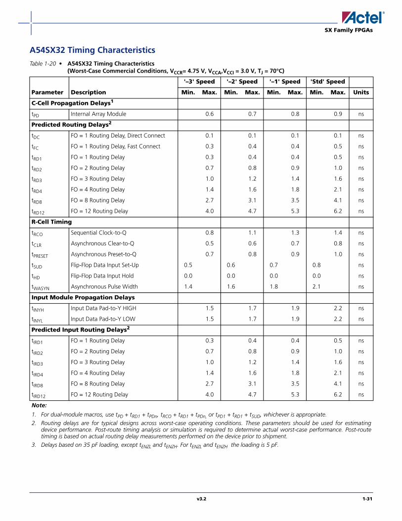
Table 1-20 • A54SX32 Timing Characteristics (Worst-Case Commercial Conditions, VCCR= 4.75 V, VCCA,VCCI = 3.0 V, TJ = 70°C)
Parameter Description
'–3' Speed '–2' Speed '–1' Speed 'Std' Speed
Min. Max. Min. Max. Min. Max. Min. Max. Units
C-Cell Propagation Delays1
tPD Internal Array Module 0.6 0.7 0.8 0.9 ns
Predicted Routing Delays2
tDC FO = 1 Routing Delay, Direct Connect 0.1 0.1 0.1 0.1 ns
tFC FO = 1 Routing Delay, Fast Connect 0.3 0.4 0.4 0.5 ns
tRD1 FO = 1 Routing Delay 0.3 0.4 0.4 0.5 ns
tRD2 FO = 2 Routing Delay 0.7 0.8 0.9 1.0 ns
tRD3 FO = 3 Routing Delay 1.0 1.2 1.4 1.6 ns
tRD4 FO = 4 Routing Delay 1.4 1.6 1.8 2.1 ns
tRD8 FO = 8 Routing Delay 2.7 3.1 3.5 4.1 ns
tRD12 FO = 12 Routing Delay 4.0 4.7 5.3 6.2 ns
R-Cell Timing
tRCO Sequential Clock-to-Q 0.8 1.1 1.3 1.4 ns
tCLR Asynchronous Clear-to-Q 0.5 0.6 0.7 0.8 ns
tPRESET Asynchronous Preset-to-Q 0.7 0.8 0.9 1.0 ns
tSUD Flip-Flop Data Input Set-Up 0.5 0.6 0.7 0.8 ns
tHD Flip-Flop Data Input Hold 0.0 0.0 0.0 0.0 ns
tWASYN Asynchronous Pulse Width 1.4 1.6 1.8 2.1 ns
Input Module Propagation Delays
tINYH Input Data Pad-to-Y HIGH 1.5 1.7 1.9 2.2 ns
tINYL Input Data Pad-to-Y LOW 1.5 1.7 1.9 2.2 ns
Predicted Input Routing Delays2
tIRD1 FO = 1 Routing Delay 0.3 0.4 0.4 0.5 ns
tIRD2 FO = 2 Routing Delay 0.7 0.8 0.9 1.0 ns
tIRD3 FO = 3 Routing Delay 1.0 1.2 1.4 1.6 ns
tIRD4 FO = 4 Routing Delay 1.4 1.6 1.8 2.1 ns
tIRD8 FO = 8 Routing Delay 2.7 3.1 3.5 4.1 ns
tIRD12 FO = 12 Routing Delay 4.0 4.7 5.3 6.2 ns
Note:
1. For dual-module macros, use tPD + tRD1 + tPDn, tRCO + tRD1 + tPDn, or tPD1 + tRD1 + tSUD, whichever is appropriate.2. Routing delays are for typical designs across worst-case operating conditions. These parameters should be used for estimating
device performance. Post-route timing analysis or simulation is required to determine actual worst-case performance. Post-routetiming is based on actual routing delay measurements performed on the device prior to shipment.
3. Delays based on 35 pF loading, except tENZL and tENZH. For tENZL and tENZH the loading is 5 pF.
v3.2 1-31

SX Family FPGAs
Dedicated (Hardwired) Array Clock Network
tHCKH Input LOW to HIGH (pad to R-Cell input) 1.9 2.1 2.4 2.8 ns
tHCKL Input HIGH to LOW (pad to R-Cell input) 1.9 2.1 2.4 2.8 ns
tHPWH Minimum Pulse Width HIGH 1.4 1.6 1.8 2.1 ns
tHPWL Minimum Pulse Width LOW 1.4 1.6 1.8 2.1 ns
tHCKSW Maximum Skew 0.3 0.4 0.4 0.5 ns
tHP Minimum Period 2.7 3.1 3.6 4.2 ns
fHMAX Maximum Frequency 350 320 280 240 MHz
Routed Array Clock Networks
tRCKH Input LOW to HIGH (light load)(pad to R-Cell input)
2.4 2.7 3.0 3.5 ns
tRCKL Input HIGH to LOW (light load)(pad to R-Cell input)
2.4 2.7 3.1 3.6 ns
tRCKH Input LOW to HIGH (50% load)(pad to R-Cell input)
2.7 3.0 3.5 4.1 ns
tRCKL Input HIGH to LOW (50% load)(pad to R-Cell input)
2.7 3.1 3.6 4.2 ns
tRCKH Input LOW to HIGH (100% load)(pad to R-Cell input)
2.7 3.1 3.5 4.1 ns
tRCKL Input HIGH to LOW (100% load)(pad to R-Cell input)
2.8 3.2 3.6 4.3 ns
tRPWH Min. Pulse Width HIGH 2.1 2.4 2.7 3.2 ns
tRPWL Min. Pulse Width LOW 2.1 2.4 2.7 3.2 ns
tRCKSW Maximum Skew (light load) 0.85 0.98 1.1 1.3 ns
tRCKSW Maximum Skew (50% load) 1.23 1.4 1.6 1.9 ns
tRCKSW Maximum Skew (100% load) 1.30 1.5 1.7 2.0 ns
TTL Output Module Timing3
tDLH Data-to-Pad LOW to HIGH 1.6 1.9 2.1 2.5 ns
tDHL Data-to-Pad HIGH to LOW 1.6 1.9 2.1 2.5 ns
tENZL Enable-to-Pad, Z to L 2.1 2.4 2.8 3.2 ns
tENZH Enable-to-Pad, Z to H 2.3 2.7 3.1 3.6 ns
tENLZ Enable-to-Pad, L to Z 1.4 1.7 1.9 2.2 ns
tENHZ Enable-to-Pad, H to Z 1.3 1.5 1.7 2.0 ns
Table 1-20 • A54SX32 Timing Characteristics (Continued)(Worst-Case Commercial Conditions, VCCR= 4.75 V, VCCA,VCCI = 3.0 V, TJ = 70°C)
Parameter Description
'–3' Speed '–2' Speed '–1' Speed 'Std' Speed
Min. Max. Min. Max. Min. Max. Min. Max. Units
Note:
1. For dual-module macros, use tPD + tRD1 + tPDn, tRCO + tRD1 + tPDn, or tPD1 + tRD1 + tSUD, whichever is appropriate.2. Routing delays are for typical designs across worst-case operating conditions. These parameters should be used for estimating
device performance. Post-route timing analysis or simulation is required to determine actual worst-case performance. Post-routetiming is based on actual routing delay measurements performed on the device prior to shipment.
3. Delays based on 35 pF loading, except tENZL and tENZH. For tENZL and tENZH the loading is 5 pF.
1-32 v3.2

SX Family FPGAs
Pin DescriptionCLKA/B Clock A and B
These pins are 3.3 V / 5.0 V PCI/TTL clock inputs for clockdistribution networks. The clock input is buffered priorto clocking the R-cells. If not used, this pin must be setLOW or HIGH on the board. It must not be left floating.(For A54SX72A, these clocks can be configured asbidirectional.)
GND Ground
LOW supply voltage.
HCLK Dedicated (hardwired) Array Clock
This pin is the 3.3 V / 5.0 V PCI/TTL clock input for sequentialmodules. This input is directly wired to each R-cell andoffers clock speeds independent of the number of R-cellsbeing driven. If not used, this pin must be set LOW orHIGH on the board. It must not be left floating.
I/O Input/Output
The I/O pin functions as an input, output, tristate, orbidirectional buffer. Based on certain configurations,input and output levels are compatible with standardTTL, LVTTL, 3.3 V PCI or 5.0 V PCI specifications. Unused I/O pins are automatically tristated by the Designer Seriessoftware.
NC No Connection
This pin is not connected to circuitry within the device.
PRA, I/O Probe A
The Probe A pin is used to output data from any user-defined design node within the device. This independentdiagnostic pin can be used in conjunction with the ProbeB pin to allow real-time diagnostic output of any signalpath within the device. The Probe A pin can be used as auser-defined I/O when verification has been completed.The pin’s probe capabilities can be permanently disabledto protect programmed design confidentiality.
PRB, I/O Probe B
The Probe B pin is used to output data from any nodewithin the device. This diagnostic pin can be used inconjunction with the Probe A pin to allow real-timediagnostic output of any signal path within the device.The Probe B pin can be used as a user-defined I/O whenverification has been completed. The pin’s probecapabilities can be permanently disabled to protectprogrammed design confidentiality.
TCK Test Clock
Test clock input for diagnostic probe and deviceprogramming. In flexible mode, TCK becomes activewhen the TMS pin is set LOW (refer to Table 1-2 onpage 1-6). This pin functions as an I/O when theboundary scan state machine reaches the "logic reset"state.
TDI Test Data Input
Serial input for boundary scan testing and diagnosticprobe. In flexible mode, TDI is active when the TMS pin isset LOW (refer to Table 1-2 on page 1-6). This pinfunctions as an I/O when the boundary scan statemachine reaches the "logic reset" state.
TDO Test Data Output
Serial output for boundary scan testing. In flexible mode,TDO is active when the TMS pin is set LOW (refer toTable 1-2 on page 1-6). This pin functions as an I/O whenthe boundary scan state machine reaches the “logicreset” state.
TMS Test Mode Select
The TMS pin controls the use of the IEEE 1149.1Boundary Scan pins (TCK, TDI, TDO). In flexible modewhen the TMS pin is set LOW, the TCK, TDI, and TDO pinsare boundary scan pins (refer to Table 1-2 on page 1-6).Once the boundary scan pins are in test mode, they willremain in that mode until the internal boundary scanstate machine reaches the "logic reset" state. At thispoint, the boundary scan pins will be released and willfunction as regular I/O pins. The "logic reset" state isreached 5 TCK cycles after the TMS pin is set HIGH. Indedicated test mode, TMS functions as specified in theIEEE 1149.1 specifications.
VCCI Supply Voltage
Supply voltage for I/Os. See Table 1-1 on page 1-5.
VCCA Supply Voltage
Supply voltage for Array. See Table 1-1 on page 1-5.
VCCR Supply Voltage
Supply voltage for input tolerance (required for internalbiasing). See Table 1-1 on page 1-5.
v3.2 1-33


54SX Family FPGAs
Package Pin Assignments
84-Pin PLCC
NoteFor Package Manufacturing and Environmental information, visit the Package Resource center athttp://www.actel.com/products/rescenter/package/index.html.
Figure 2-1 • 84-Pin PLCC (Top View)
1 84
84-PinPLCC
v3.2 2-1

54SX Family FPGAs
84-Pin PLCC
Pin NumberA54SX08 Function
1 VCCR
2 GND
3 VCCA
4 PRA, I/O
5 I/O
6 I/O
7 VCCI
8 I/O
9 I/O
10 I/O
11 TCK, I/O
12 TDI, I/O
13 I/O
14 I/O
15 I/O
16 TMS
17 I/O
18 I/O
19 I/O
20 I/O
21 I/O
22 I/O
23 I/O
24 I/O
25 I/O
26 I/O
27 GND
28 VCCI
29 I/O
30 I/O
31 I/O
32 I/O
33 I/O
34 I/O
35 I/O
36 I/O
37 I/O
38 I/O
39 I/O
40 PRB, I/O
41 VCCA
42 GND
43 VCCR
44 I/O
45 HCLK
46 I/O
47 I/O
48 I/O
49 I/O
50 I/O
51 I/O
52 TDO, I/O
53 I/O
54 I/O
55 I/O
56 I/O
57 I/O
58 I/O
59 VCCA
60 VCCI
61 GND
62 I/O
63 I/O
64 I/O
65 I/O
66 I/O
67 I/O
68 VCCA
69 GND
70 I/O
84-Pin PLCC
Pin NumberA54SX08 Function
71 I/O
72 I/O
73 I/O
74 I/O
75 I/O
76 I/O
77 I/O
78 I/O
79 I/O
80 I/O
81 I/O
82 I/O
83 CLKA
84 CLKB
84-Pin PLCC
Pin NumberA54SX08 Function
2-2 v3.2
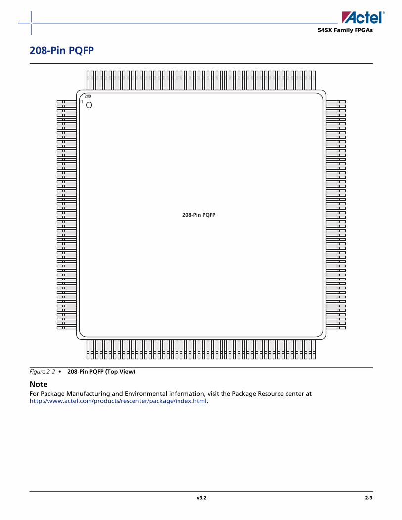
54SX Family FPGAs
208-Pin PQFP
NoteFor Package Manufacturing and Environmental information, visit the Package Resource center athttp://www.actel.com/products/rescenter/package/index.html.
Figure 2-2 • 208-Pin PQFP (Top View)
208-Pin PQFP
1208
v3.2 2-3
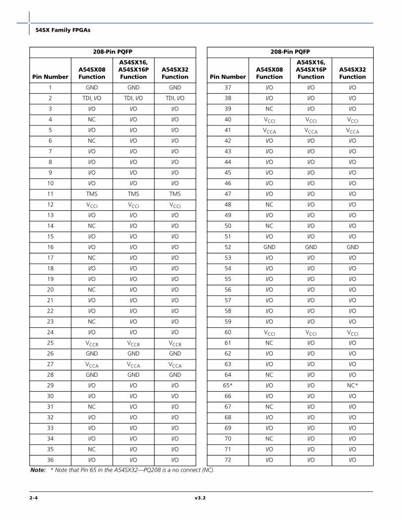
54SX Family FPGAs
208-Pin PQFP
Pin NumberA54SX08 Function
A54SX16, A54SX16P Function
A54SX32 Function
1 GND GND GND
2 TDI, I/O TDI, I/O TDI, I/O
3 I/O I/O I/O
4 NC I/O I/O
5 I/O I/O I/O
6 NC I/O I/O
7 I/O I/O I/O
8 I/O I/O I/O
9 I/O I/O I/O
10 I/O I/O I/O
11 TMS TMS TMS
12 VCCI VCCI VCCI
13 I/O I/O I/O
14 NC I/O I/O
15 I/O I/O I/O
16 I/O I/O I/O
17 NC I/O I/O
18 I/O I/O I/O
19 I/O I/O I/O
20 NC I/O I/O
21 I/O I/O I/O
22 I/O I/O I/O
23 NC I/O I/O
24 I/O I/O I/O
25 VCCR VCCR VCCR
26 GND GND GND
27 VCCA VCCA VCCA
28 GND GND GND
29 I/O I/O I/O
30 I/O I/O I/O
31 NC I/O I/O
32 I/O I/O I/O
33 I/O I/O I/O
34 I/O I/O I/O
35 NC I/O I/O
36 I/O I/O I/O
37 I/O I/O I/O
38 I/O I/O I/O
39 NC I/O I/O
40 VCCI VCCI VCCI
41 VCCA VCCA VCCA
42 I/O I/O I/O
43 I/O I/O I/O
44 I/O I/O I/O
45 I/O I/O I/O
46 I/O I/O I/O
47 I/O I/O I/O
48 NC I/O I/O
49 I/O I/O I/O
50 NC I/O I/O
51 I/O I/O I/O
52 GND GND GND
53 I/O I/O I/O
54 I/O I/O I/O
55 I/O I/O I/O
56 I/O I/O I/O
57 I/O I/O I/O
58 I/O I/O I/O
59 I/O I/O I/O
60 VCCI VCCI VCCI
61 NC I/O I/O
62 I/O I/O I/O
63 I/O I/O I/O
64 NC I/O I/O
65* I/O I/O NC*
66 I/O I/O I/O
67 NC I/O I/O
68 I/O I/O I/O
69 I/O I/O I/O
70 NC I/O I/O
71 I/O I/O I/O
72 I/O I/O I/O
208-Pin PQFP
Pin NumberA54SX08 Function
A54SX16, A54SX16P Function
A54SX32 Function
Note: * Note that Pin 65 in the A54SX32—PQ208 is a no connect (NC).
2-4 v3.2

54SX Family FPGAs
73 NC I/O I/O
74 I/O I/O I/O
75 NC I/O I/O
76 PRB, I/O PRB, I/O PRB, I/O
77 GND GND GND
78 VCCA VCCA VCCA
79 GND GND GND
80 VCCR VCCR VCCR
81 I/O I/O I/O
82 HCLK HCLK HCLK
83 I/O I/O I/O
84 I/O I/O I/O
85 NC I/O I/O
86 I/O I/O I/O
87 I/O I/O I/O
88 NC I/O I/O
89 I/O I/O I/O
90 I/O I/O I/O
91 NC I/O I/O
92 I/O I/O I/O
93 I/O I/O I/O
94 NC I/O I/O
95 I/O I/O I/O
96 I/O I/O I/O
97 NC I/O I/O
98 VCCI VCCI VCCI
99 I/O I/O I/O
100 I/O I/O I/O
101 I/O I/O I/O
102 I/O I/O I/O
103 TDO, I/O TDO, I/O TDO, I/O
104 I/O I/O I/O
105 GND GND GND
106 NC I/O I/O
107 I/O I/O I/O
108 NC I/O I/O
208-Pin PQFP
Pin NumberA54SX08 Function
A54SX16, A54SX16P Function
A54SX32 Function
109 I/O I/O I/O
110 I/O I/O I/O
111 I/O I/O I/O
112 I/O I/O I/O
113 I/O I/O I/O
114 VCCA VCCA VCCA
115 VCCI VCCI VCCI
116 NC I/O I/O
117 I/O I/O I/O
118 I/O I/O I/O
119 NC I/O I/O
120 I/O I/O I/O
121 I/O I/O I/O
122 NC I/O I/O
123 I/O I/O I/O
124 I/O I/O I/O
125 NC I/O I/O
126 I/O I/O I/O
127 I/O I/O I/O
128 I/O I/O I/O
129 GND GND GND
130 VCCA VCCA VCCA
131 GND GND GND
132 VCCR VCCR VCCR
133 I/O I/O I/O
134 I/O I/O I/O
135 NC I/O I/O
136 I/O I/O I/O
137 I/O I/O I/O
138 NC I/O I/O
139 I/O I/O I/O
140 I/O I/O I/O
141 NC I/O I/O
142 I/O I/O I/O
143 NC I/O I/O
144 I/O I/O I/O
208-Pin PQFP
Pin NumberA54SX08 Function
A54SX16, A54SX16P Function
A54SX32 Function
Note: * Note that Pin 65 in the A54SX32—PQ208 is a no connect (NC).
v3.2 2-5
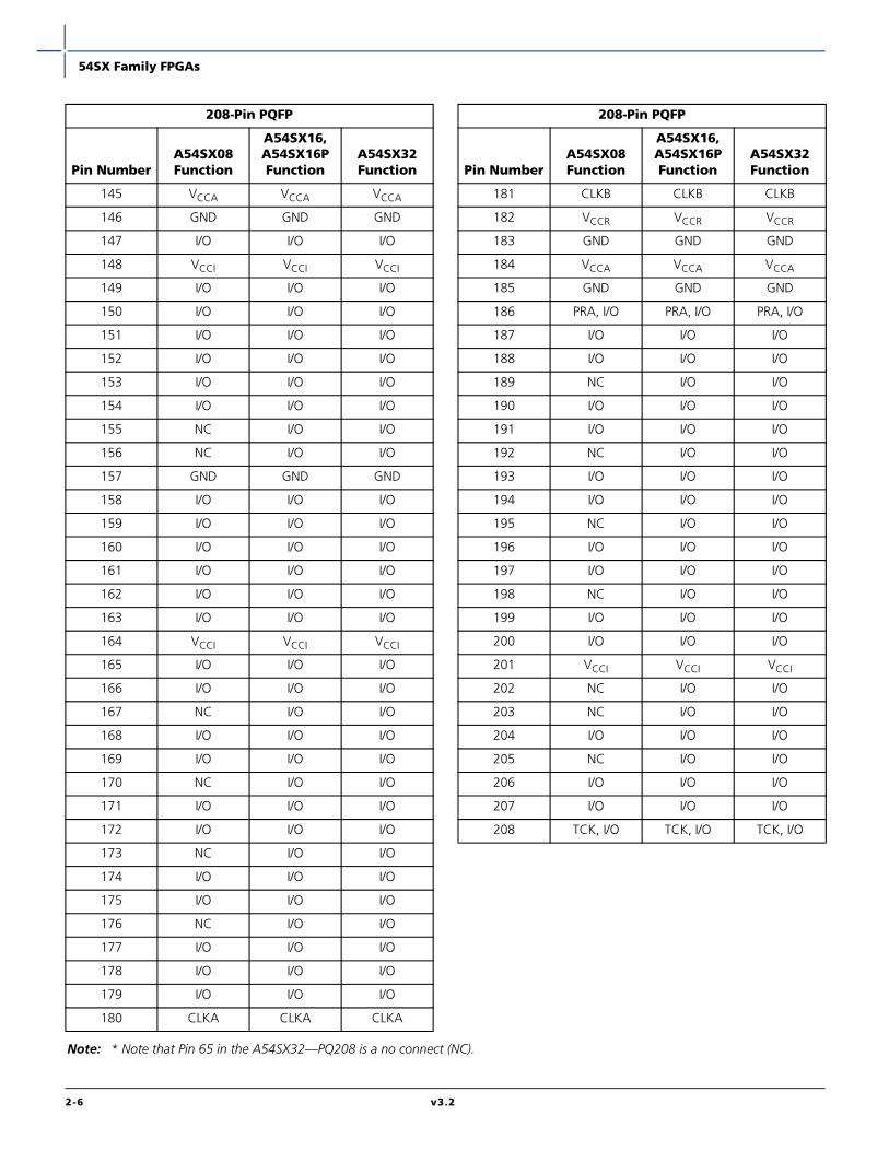
54SX Family FPGAs
145 VCCA VCCA VCCA
146 GND GND GND
147 I/O I/O I/O
148 VCCI VCCI VCCI
149 I/O I/O I/O
150 I/O I/O I/O
151 I/O I/O I/O
152 I/O I/O I/O
153 I/O I/O I/O
154 I/O I/O I/O
155 NC I/O I/O
156 NC I/O I/O
157 GND GND GND
158 I/O I/O I/O
159 I/O I/O I/O
160 I/O I/O I/O
161 I/O I/O I/O
162 I/O I/O I/O
163 I/O I/O I/O
164 VCCI VCCI VCCI
165 I/O I/O I/O
166 I/O I/O I/O
167 NC I/O I/O
168 I/O I/O I/O
169 I/O I/O I/O
170 NC I/O I/O
171 I/O I/O I/O
172 I/O I/O I/O
173 NC I/O I/O
174 I/O I/O I/O
175 I/O I/O I/O
176 NC I/O I/O
177 I/O I/O I/O
178 I/O I/O I/O
179 I/O I/O I/O
180 CLKA CLKA CLKA
208-Pin PQFP
Pin NumberA54SX08 Function
A54SX16, A54SX16P Function
A54SX32 Function
181 CLKB CLKB CLKB
182 VCCR VCCR VCCR
183 GND GND GND
184 VCCA VCCA VCCA
185 GND GND GND
186 PRA, I/O PRA, I/O PRA, I/O
187 I/O I/O I/O
188 I/O I/O I/O
189 NC I/O I/O
190 I/O I/O I/O
191 I/O I/O I/O
192 NC I/O I/O
193 I/O I/O I/O
194 I/O I/O I/O
195 NC I/O I/O
196 I/O I/O I/O
197 I/O I/O I/O
198 NC I/O I/O
199 I/O I/O I/O
200 I/O I/O I/O
201 VCCI VCCI VCCI
202 NC I/O I/O
203 NC I/O I/O
204 I/O I/O I/O
205 NC I/O I/O
206 I/O I/O I/O
207 I/O I/O I/O
208 TCK, I/O TCK, I/O TCK, I/O
208-Pin PQFP
Pin NumberA54SX08 Function
A54SX16, A54SX16P Function
A54SX32 Function
Note: * Note that Pin 65 in the A54SX32—PQ208 is a no connect (NC).
2-6 v3.2
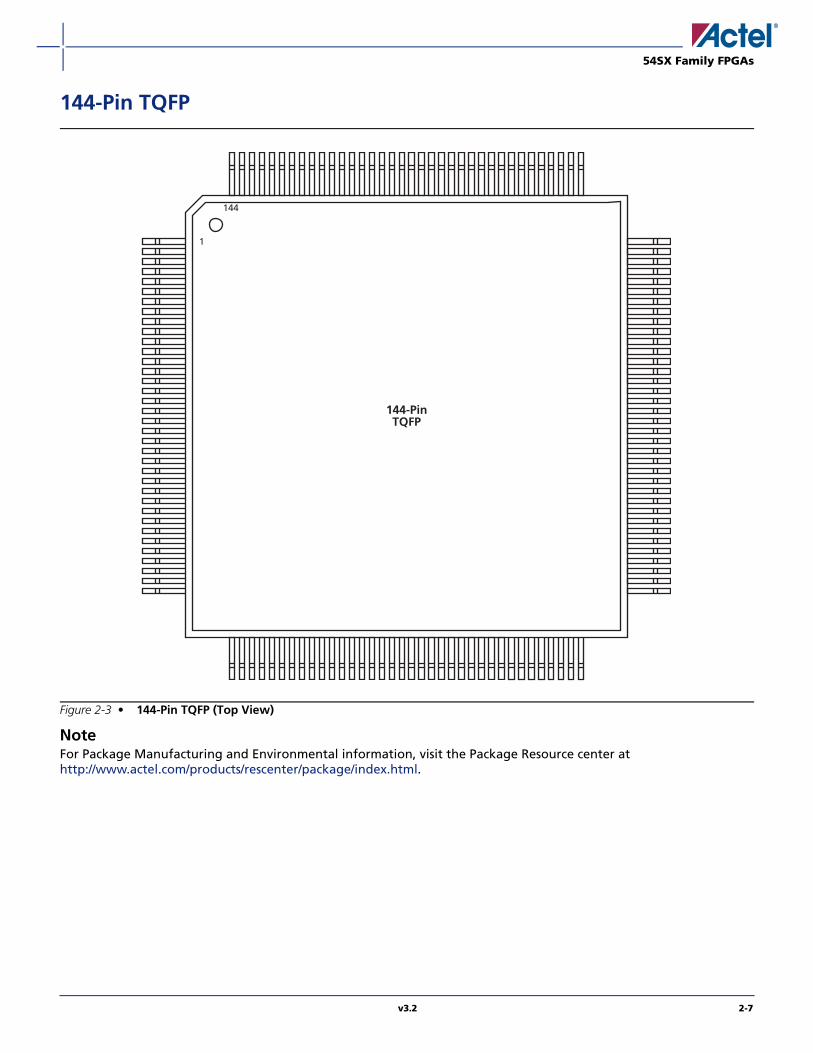
54SX Family FPGAs
144-Pin TQFP
NoteFor Package Manufacturing and Environmental information, visit the Package Resource center athttp://www.actel.com/products/rescenter/package/index.html.
Figure 2-3 • 144-Pin TQFP (Top View)
1
144
144-PinTQFP
v3.2 2-7

54SX Family FPGAs
144-Pin TQFP
Pin NumberA54SX08 Function
A54SX16P Function
A54SX32 Function
1 GND GND GND
2 TDI, I/O TDI, I/O TDI, I/O
3 I/O I/O I/O
4 I/O I/O I/O
5 I/O I/O I/O
6 I/O I/O I/O
7 I/O I/O I/O
8 I/O I/O I/O
9 TMS TMS TMS
10 VCCI VCCI VCCI
11 GND GND GND
12 I/O I/O I/O
13 I/O I/O I/O
14 I/O I/O I/O
15 I/O I/O I/O
16 I/O I/O I/O
17 I/O I/O I/O
18 I/O I/O I/O
19 VCCR VCCR VCCR
20 VCCA VCCA VCCA
21 I/O I/O I/O
22 I/O I/O I/O
23 I/O I/O I/O
24 I/O I/O I/O
25 I/O I/O I/O
26 I/O I/O I/O
27 I/O I/O I/O
28 GND GND GND
29 VCCI VCCI VCCI
30 VCCA VCCA VCCA
31 I/O I/O I/O
32 I/O I/O I/O
33 I/O I/O I/O
34 I/O I/O I/O
35 I/O I/O I/O
36 GND GND GND
37 I/O I/O I/O
38 I/O I/O I/O
39 I/O I/O I/O
40 I/O I/O I/O
41 I/O I/O I/O
42 I/O I/O I/O
43 I/O I/O I/O
44 VCCI VCCI VCCI
45 I/O I/O I/O
46 I/O I/O I/O
47 I/O I/O I/O
48 I/O I/O I/O
49 I/O I/O I/O
50 I/O I/O I/O
51 I/O I/O I/O
52 I/O I/O I/O
53 I/O I/O I/O
54 PRB, I/O PRB, I/O PRB, I/O
55 I/O I/O I/O
56 VCCA VCCA VCCA
57 GND GND GND
58 VCCR VCCR VCCR
59 I/O I/O I/O
60 HCLK HCLK HCLK
61 I/O I/O I/O
62 I/O I/O I/O
63 I/O I/O I/O
64 I/O I/O I/O
65 I/O I/O I/O
66 I/O I/O I/O
67 I/O I/O I/O
68 VCCI VCCI VCCI
69 I/O I/O I/O
70 I/O I/O I/O
71 TDO, I/O TDO, I/O TDO, I/O
72 I/O I/O I/O
144-Pin TQFP
Pin NumberA54SX08 Function
A54SX16P Function
A54SX32 Function
2-8 v3.2

54SX Family FPGAs
73 GND GND GND
74 I/O I/O I/O
75 I/O I/O I/O
76 I/O I/O I/O
77 I/O I/O I/O
78 I/O I/O I/O
79 VCCA VCCA VCCA
80 VCCI VCCI VCCI
81 GND GND GND
82 I/O I/O I/O
83 I/O I/O I/O
84 I/O I/O I/O
85 I/O I/O I/O
86 I/O I/O I/O
87 I/O I/O I/O
88 I/O I/O I/O
89 VCCA VCCA VCCA
90 VCCR VCCR VCCR
91 I/O I/O I/O
92 I/O I/O I/O
93 I/O I/O I/O
94 I/O I/O I/O
95 I/O I/O I/O
96 I/O I/O I/O
97 I/O I/O I/O
98 VCCA VCCA VCCA
99 GND GND GND
100 I/O I/O I/O
101 GND GND GND
102 VCCI VCCI VCCI
103 I/O I/O I/O
104 I/O I/O I/O
105 I/O I/O I/O
106 I/O I/O I/O
107 I/O I/O I/O
108 I/O I/O I/O
144-Pin TQFP
Pin NumberA54SX08 Function
A54SX16P Function
A54SX32 Function
109 GND GND GND
110 I/O I/O I/O
111 I/O I/O I/O
112 I/O I/O I/O
113 I/O I/O I/O
114 I/O I/O I/O
115 VCCI VCCI VCCI
116 I/O I/O I/O
117 I/O I/O I/O
118 I/O I/O I/O
119 I/O I/O I/O
120 I/O I/O I/O
121 I/O I/O I/O
122 I/O I/O I/O
123 I/O I/O I/O
124 I/O I/O I/O
125 CLKA CLKA CLKA
126 CLKB CLKB CLKB
127 VCCR VCCR VCCR
128 GND GND GND
129 VCCA VCCA VCCA
130 I/O I/O I/O
131 PRA, I/O PRA, I/O PRA, I/O
132 I/O I/O I/O
133 I/O I/O I/O
134 I/O I/O I/O
135 I/O I/O I/O
136 I/O I/O I/O
137 I/O I/O I/O
138 I/O I/O I/O
139 I/O I/O I/O
140 VCCI VCCI VCCI
141 I/O I/O I/O
142 I/O I/O I/O
143 I/O I/O I/O
144 TCK, I/O TCK, I/O TCK, I/O
144-Pin TQFP
Pin NumberA54SX08 Function
A54SX16P Function
A54SX32 Function
v3.2 2-9

54SX Family FPGAs
176-Pin TQFP
NoteFor Package Manufacturing and Environmental information, visit the Package Resource center athttp://www.actel.com/products/rescenter/package/index.html.
Figure 2-4 • 176-Pin TQFP (Top View)
176-PinTQFP
1761
2-10 v3.2

54SX Family FPGAs
176-Pin TQFP
Pin NumberA54SX08 Function
A54SX16, A54SX16P Function
A54SX32 Function
1 GND GND GND
2 TDI, I/O TDI, I/O TDI, I/O
3 NC I/O I/O
4 I/O I/O I/O
5 I/O I/O I/O
6 I/O I/O I/O
7 I/O I/O I/O
8 I/O I/O I/O
9 I/O I/O I/O
10 TMS TMS TMS
11 VCCI VCCI VCCI
12 NC I/O I/O
13 I/O I/O I/O
14 I/O I/O I/O
15 I/O I/O I/O
16 I/O I/O I/O
17 I/O I/O I/O
18 I/O I/O I/O
19 I/O I/O I/O
20 I/O I/O I/O
21 GND GND GND
22 VCCA VCCA VCCA
23 GND GND GND
24 I/O I/O I/O
25 I/O I/O I/O
26 I/O I/O I/O
27 I/O I/O I/O
28 I/O I/O I/O
29 I/O I/O I/O
30 I/O I/O I/O
31 I/O I/O I/O
32 VCCI VCCI VCCI
33 VCCA VCCA VCCA
34 I/O I/O I/O
35 I/O I/O I/O
36 I/O I/O I/O
37 I/O I/O I/O
38 I/O I/O I/O
39 I/O I/O I/O
40 NC I/O I/O
41 I/O I/O I/O
42 NC I/O I/O
43 I/O I/O I/O
44 GND GND GND
45 I/O I/O I/O
46 I/O I/O I/O
47 I/O I/O I/O
48 I/O I/O I/O
49 I/O I/O I/O
50 I/O I/O I/O
51 I/O I/O I/O
52 VCCI VCCI VCCI
53 I/O I/O I/O
54 NC I/O I/O
55 I/O I/O I/O
56 I/O I/O I/O
57 NC I/O I/O
58 I/O I/O I/O
59 I/O I/O I/O
60 I/O I/O I/O
61 I/O I/O I/O
62 I/O I/O I/O
63 I/O I/O I/O
64 PRB, I/O PRB, I/O PRB, I/O
65 GND GND GND
66 VCCA VCCA VCCA
67 VCCR VCCR VCCR
68 I/O I/O I/O
176-Pin TQFP
Pin NumberA54SX08 Function
A54SX16, A54SX16P Function
A54SX32 Function
v3.2 2-11
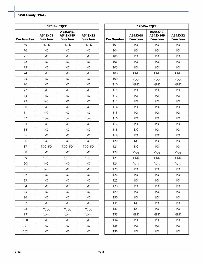
54SX Family FPGAs
69 HCLK HCLK HCLK
70 I/O I/O I/O
71 I/O I/O I/O
72 I/O I/O I/O
73 I/O I/O I/O
74 I/O I/O I/O
75 I/O I/O I/O
76 I/O I/O I/O
77 I/O I/O I/O
78 I/O I/O I/O
79 NC I/O I/O
80 I/O I/O I/O
81 NC I/O I/O
82 VCCI VCCI VCCI
83 I/O I/O I/O
84 I/O I/O I/O
85 I/O I/O I/O
86 I/O I/O I/O
87 TDO, I/O TDO, I/O TDO, I/O
88 I/O I/O I/O
89 GND GND GND
90 NC I/O I/O
91 NC I/O I/O
92 I/O I/O I/O
93 I/O I/O I/O
94 I/O I/O I/O
95 I/O I/O I/O
96 I/O I/O I/O
97 I/O I/O I/O
98 VCCA VCCA VCCA
99 VCCI VCCI VCCI
100 I/O I/O I/O
101 I/O I/O I/O
102 I/O I/O I/O
176-Pin TQFP
Pin NumberA54SX08 Function
A54SX16, A54SX16P Function
A54SX32 Function
103 I/O I/O I/O
104 I/O I/O I/O
105 I/O I/O I/O
106 I/O I/O I/O
107 I/O I/O I/O
108 GND GND GND
109 VCCA VCCA VCCA
110 GND GND GND
111 I/O I/O I/O
112 I/O I/O I/O
113 I/O I/O I/O
114 I/O I/O I/O
115 I/O I/O I/O
116 I/O I/O I/O
117 I/O I/O I/O
118 NC I/O I/O
119 I/O I/O I/O
120 NC I/O I/O
121 NC I/O I/O
122 VCCA VCCA VCCA
123 GND GND GND
124 VCCI VCCI VCCI
125 I/O I/O I/O
126 I/O I/O I/O
127 I/O I/O I/O
128 I/O I/O I/O
129 I/O I/O I/O
130 I/O I/O I/O
131 NC I/O I/O
132 NC I/O I/O
133 GND GND GND
134 I/O I/O I/O
135 I/O I/O I/O
136 I/O I/O I/O
176-Pin TQFP
Pin NumberA54SX08 Function
A54SX16, A54SX16P Function
A54SX32 Function
2-12 v3.2

54SX Family FPGAs
137 I/O I/O I/O
138 I/O I/O I/O
139 I/O I/O I/O
140 VCCI VCCI VCCI
141 I/O I/O I/O
142 I/O I/O I/O
143 I/O I/O I/O
144 I/O I/O I/O
145 I/O I/O I/O
146 I/O I/O I/O
147 I/O I/O I/O
148 I/O I/O I/O
149 I/O I/O I/O
150 I/O I/O I/O
151 I/O I/O I/O
152 CLKA CLKA CLKA
153 CLKB CLKB CLKB
154 VCCR VCCR VCCR
155 GND GND GND
156 VCCA VCCA VCCA
176-Pin TQFP
Pin NumberA54SX08 Function
A54SX16, A54SX16P Function
A54SX32 Function
157 PRA, I/O PRA, I/O PRA, I/O
158 I/O I/O I/O
159 I/O I/O I/O
160 I/O I/O I/O
161 I/O I/O I/O
162 I/O I/O I/O
163 I/O I/O I/O
164 I/O I/O I/O
165 I/O I/O I/O
166 I/O I/O I/O
167 I/O I/O I/O
168 NC I/O I/O
169 VCCI VCCI VCCI
170 I/O I/O I/O
171 NC I/O I/O
172 NC I/O I/O
173 NC I/O I/O
174 I/O I/O I/O
175 I/O I/O I/O
176 TCK, I/O TCK, I/O TCK, I/O
176-Pin TQFP
Pin NumberA54SX08 Function
A54SX16, A54SX16P Function
A54SX32 Function
v3.2 2-13
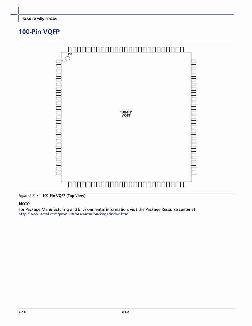
54SX Family FPGAs
100-Pin VQFP
NoteFor Package Manufacturing and Environmental information, visit the Package Resource center athttp://www.actel.com/products/rescenter/package/index.html.
Figure 2-5 • 100-Pin VQFP (Top View)
1
100-PinVQFP
100
2-14 v3.2

54SX Family FPGAs
100-Pin VQFP
Pin Number
A54SX08 Function
A54SX16, A54SX16P Function
1 GND GND
2 TDI, I/O TDI, I/O
3 I/O I/O
4 I/O I/O
5 I/O I/O
6 I/O I/O
7 TMS TMS
8 VCCI VCCI
9 GND GND
10 I/O I/O
11 I/O I/O
12 I/O I/O
13 I/O I/O
14 I/O I/O
15 I/O I/O
16 I/O I/O
17 I/O I/O
18 I/O I/O
19 I/O I/O
20 VCCI VCCI
21 I/O I/O
22 I/O I/O
23 I/O I/O
24 I/O I/O
25 I/O I/O
26 I/O I/O
27 I/O I/O
28 I/O I/O
29 I/O I/O
30 I/O I/O
31 I/O I/O
32 I/O I/O
33 I/O I/O
34 PRB, I/O PRB, I/O
35 VCCA VCCA
36 GND GND
37 VCCR VCCR
38 I/O I/O
39 HCLK HCLK
40 I/O I/O
41 I/O I/O
42 I/O I/O
43 I/O I/O
44 VCCI VCCI
45 I/O I/O
46 I/O I/O
47 I/O I/O
48 I/O I/O
49 TDO, I/O TDO, I/O
50 I/O I/O
51 GND GND
52 I/O I/O
53 I/O I/O
54 I/O I/O
55 I/O I/O
56 I/O I/O
57 VCCA VCCA
58 VCCI VCCI
59 I/O I/O
60 I/O I/O
61 I/O I/O
62 I/O I/O
63 I/O I/O
64 I/O I/O
65 I/O I/O
66 I/O I/O
67 VCCA VCCA
68 GND GND
100-Pin VQFP
Pin Number
A54SX08 Function
A54SX16, A54SX16P Function
69 GND GND
70 I/O I/O
71 I/O I/O
72 I/O I/O
73 I/O I/O
74 I/O I/O
75 I/O I/O
76 I/O I/O
77 I/O I/O
78 I/O I/O
79 I/O I/O
80 I/O I/O
81 I/O I/O
82 VCCI VCCI
83 I/O I/O
84 I/O I/O
85 I/O I/O
86 I/O I/O
87 CLKA CLKA
88 CLKB CLKB
89 VCCR VCCR
90 VCCA VCCA
91 GND GND
92 PRA, I/O PRA, I/O
93 I/O I/O
94 I/O I/O
95 I/O I/O
96 I/O I/O
97 I/O I/O
98 I/O I/O
99 I/O I/O
100 TCK, I/O TCK, I/O
100-Pin VQFP
Pin Number
A54SX08 Function
A54SX16, A54SX16P Function
v3.2 2-15

54SX Family FPGAs
313-Pin PBGA
NoteFor Package Manufacturing and Environmental information, visit the Package Resource center athttp://www.actel.com/products/rescenter/package/index.html.
Figure 2-6 • 313-Pin PBGA (Top View)
1 2 3 4 5 6 7 8 9 10 11 12 13 14 15
ABC
D
EFG
HJ
KL
MNPR
TU
VW
YAA
ABAC
ADAE
ABC
D
EFG
HJ
KL
MNPR
TU
VW
YAA
ABAC
ADAE
16 17 18 19 20 21 22 23 24 25
1 2 3 4 5 6 7 8 9 10 11 12 13 14 15 16 17 18 19 20 21 22 23 24 25
2-16 v3.2

54SX Family FPGAs
313-Pin PBGA
Pin Number
A54SX32 Function
A1 GND
A3 NC
A5 I/O
A7 I/O
A9 I/O
A11 I/O
A13 VCCR
A15 I/O
A17 I/O
A19 I/O
A21 I/O
A23 NC
A25 GND
AA1 I/O
AA3 I/O
AA5 NC
AA7 I/O
AA9 NC
AA11 I/O
AA13 I/O
AA15 I/O
AA17 I/O
AA19 I/O
AA21 I/O
AA23 NC
AA25 I/O
AB2 NC
AB4 NC
AB6 I/O
AB8 I/O
AB10 I/O
AB12 I/O
AB14 I/O
AB16 I/O
AB18 VCCI
AB20 NC
AB22 I/O
AB24 I/O
AC1 I/O
AC3 I/O
AC5 I/O
AC7 I/O
AC9 I/O
AC11 I/O
AC13 VCCR
AC15 I/O
AC17 I/O
AC19 I/O
AC21 I/O
AC23 I/O
AC25 NC
AD2 GND
AD4 I/O
AD6 VCCI
AD8 I/O
AD10 I/O
AD12 PRB, I/O
AD14 I/O
AD16 I/O
AD18 I/O
AD20 I/O
AD22 NC
AD24 I/O
AE1 NC
AE3 I/O
AE5 I/O
AE7 I/O
AE9 I/O
AE11 I/O
AE13 VCCA
AE15 I/O
AE17 I/O
AE19 I/O
AE21 I/O
AE23 TDO, I/O
AE25 GND
B2 TCK, I/O
B4 I/O
B6 I/O
B8 I/O
313-Pin PBGA
Pin Number
A54SX32 Function
B10 I/O
B12 I/O
B14 I/O
B16 I/O
B18 I/O
B20 I/O
B22 I/O
B24 I/O
C1 TDI, I/O
C3 I/O
C5 NC
C7 I/O
C9 I/O
C11 I/O
C13 VCCI
C15 I/O
C17 I/O
C19 VCCI
C21 I/O
C23 I/O
C25 NC
D2 I/O
D4 NC
D6 I/O
D8 I/O
D10 I/O
D12 I/O
D14 I/O
D16 I/O
D18 I/O
D20 I/O
D22 I/O
D24 NC
E1 I/O
E3 NC
E5 I/O
E7 I/O
E9 I/O
E11 I/O
E13 VCCA
313-Pin PBGA
Pin Number
A54SX32 Function
E15 I/O
E17 I/O
E19 I/O
E21 I/O
E23 I/O
E25 I/O
F2 I/O
F4 I/O
F6 NC
F8 I/O
F10 NC
F12 I/O
F14 I/O
F16 NC
F18 I/O
F20 I/O
F22 I/O
F24 I/O
G1 I/O
G3 TMS
G5 I/O
G7 I/O
G9 VCCI
G11 I/O
G13 CLKB
G15 I/O
G17 I/O
G19 I/O
G21 I/O
G23 I/O
G25 I/O
H2 I/O
H4 I/O
H6 I/O
H8 I/O
H10 I/O
H12 PRA, I/O
H14 I/O
H16 I/O
H18 NC
313-Pin PBGA
Pin Number
A54SX32 Function
v3.2 2-17

54SX Family FPGAs
H20 I/O
H22 VCCI
H24 I/O
J1 I/O
J3 I/O
J5 I/O
J7 NC
J9 I/O
J11 I/O
J13 CLKA
J15 I/O
J17 I/O
J19 I/O
J21 GND
J23 I/O
J25 I/O
K2 I/O
K4 I/O
K6 I/O
K8 VCCI
K10 I/O
K12 I/O
K14 I/O
K16 I/O
K18 I/O
K20 VCCA
K22 I/O
K24 I/O
L1 I/O
L3 I/O
L5 I/O
L7 I/O
L9 I/O
L11 I/O
L13 GND
L15 I/O
L17 I/O
L19 I/O
L21 I/O
L23 I/O
313-Pin PBGA
Pin Number
A54SX32 Function
L25 I/O
M2 I/O
M4 I/O
M6 I/O
M8 I/O
M10 I/O
M12 GND
M14 GND
M16 VCCI
M18 I/O
M20 I/O
M22 I/O
M24 I/O
N1 I/O
N3 VCCA
N5 VCCR
N7 I/O
N9 VCCI
N11 GND
N13 GND
N15 GND
N17 I/O
N19 I/O
N21 I/O
N23 VCCR
N25 VCCA
P2 I/O
P4 I/O
P6 I/O
P8 I/O
P10 I/O
P12 GND
P14 GND
P16 I/O
P18 I/O
P20 NC
P22 I/O
P24 I/O
R1 I/O
R3 I/O
313-Pin PBGA
Pin Number
A54SX32 Function
R5 I/O
R7 I/O
R9 I/O
R11 I/O
R13 GND
R15 I/O
R17 I/O
R19 I/O
R21 I/O
R23 I/O
R25 I/O
T2 I/O
T4 I/O
T6 I/O
T8 I/O
T10 I/O
T12 I/O
T14 HCLK
T16 I/O
T18 I/O
T20 I/O
T22 I/O
T24 I/O
U1 I/O
U3 I/O
U5 VCCI
U7 I/O
U9 I/O
U11 I/O
U13 I/O
U15 I/O
U17 I/O
U19 I/O
U21 I/O
U23 I/O
U25 I/O
V2 VCCA
V4 I/O
V6 I/O
V8 I/O
313-Pin PBGA
Pin Number
A54SX32 Function
V10 I/O
V12 I/O
V14 I/O
V16 NC
V18 I/O
V20 I/O
V22 VCCA
V24 VCCI
W1 I/O
W3 I/O
W5 I/O
W7 NC
W9 I/O
W11 I/O
W13 VCCI
W15 I/O
W17 I/O
W19 I/O
W21 I/O
W23 I/O
W25 I/O
Y2 I/O
Y4 I/O
Y6 I/O
Y8 I/O
Y10 I/O
Y12 I/O
Y14 I/O
Y16 I/O
Y18 I/O
Y20 NC
Y22 I/O
Y24 NC
313-Pin PBGA
Pin Number
A54SX32 Function
2-18 v3.2
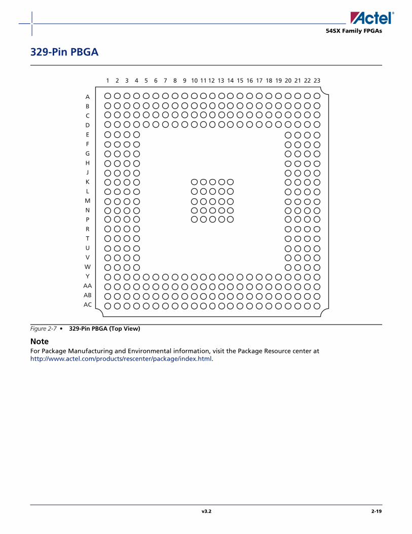
54SX Family FPGAs
329-Pin PBGA
NoteFor Package Manufacturing and Environmental information, visit the Package Resource center athttp://www.actel.com/products/rescenter/package/index.html.
Figure 2-7 • 329-Pin PBGA (Top View)
2322212019181716151410 11 12 13987654321
A
B
C
D
E
F
G
H
J
K
L
M
N
P
R
T
U
V
W
Y
AA
AB
AC
v3.2 2-19

54SX Family FPGAs
329-Pin PBGA
Pin Number
A54SX32 Function
A1 GND
A2 GND
A3 VCCI
A4 NC
A5 I/O
A6 I/O
A7 VCCI
A8 NC
A9 I/O
A10 I/O
A11 I/O
A12 I/O
A13 CLKB
A14 I/O
A15 I/O
A16 I/O
A17 I/O
A18 I/O
A19 I/O
A20 I/O
A21 NC
A22 VCCI
A23 GND
AA1 VCCI
AA2 I/O
AA3 GND
AA4 I/O
AA5 I/O
AA6 I/O
AA7 I/O
AA8 I/O
AA9 I/O
AA10 I/O
AA11 I/O
AA12 I/O
AA13 I/O
AA14 I/O
AA15 I/O
AA16 I/O
AA17 I/O
AA18 I/O
AA19 I/O
AA20 TDO, I/O
AA21 VCCI
AA22 I/O
AA23 VCCI
AB1 I/O
AB2 GND
AB3 I/O
AB4 I/O
AB5 I/O
AB6 I/O
AB7 I/O
AB8 I/O
AB9 I/O
AB10 I/O
AB11 PRB, I/O
AB12 I/O
AB13 HCLK
AB14 I/O
AB15 I/O
AB16 I/O
AB17 I/O
AB18 I/O
AB19 I/O
AB20 I/O
AB21 I/O
AB22 GND
AB23 I/O
AC1 GND
329-Pin PBGA
Pin Number
A54SX32 Function
AC2 VCCI
AC3 NC
AC4 I/O
AC5 I/O
AC6 I/O
AC7 I/O
AC8 I/O
AC9 VCCI
AC10 I/O
AC11 I/O
AC12 I/O
AC13 I/O
AC14 I/O
AC15 NC
AC16 I/O
AC17 I/O
AC18 I/O
AC19 I/O
AC20 I/O
AC21 NC
AC22 VCCI
AC23 GND
B1 VCCI
B2 GND
B3 I/O
B4 I/O
B5 I/O
B6 I/O
B7 I/O
B8 I/O
B9 I/O
B10 I/O
B11 I/O
B12 PRA, I/O
B13 CLKA
329-Pin PBGA
Pin Number
A54SX32 Function
B14 I/O
B15 I/O
B16 I/O
B17 I/O
B18 I/O
B19 I/O
B20 I/O
B21 I/O
B22 GND
B23 VCCI
C1 NC
C2 TDI, I/O
C3 GND
C4 I/O
C5 I/O
C6 I/O
C7 I/O
C8 I/O
C9 I/O
C10 I/O
C11 I/O
C12 I/O
C13 I/O
C14 I/O
C15 I/O
C16 I/O
C17 I/O
C18 I/O
C19 I/O
C20 I/O
C21 VCCI
C22 GND
C23 NC
D1 I/O
D2 I/O
329-Pin PBGA
Pin Number
A54SX32 Function
2-20 v3.2

54SX Family FPGAs
D3 I/O
D4 TCK, I/O
D5 I/O
D6 I/O
D7 I/O
D8 I/O
D9 I/O
D10 I/O
D11 VCCA
D12 VCCR
D13 I/O
D14 I/O
D15 I/O
D16 I/O
D17 I/O
D18 I/O
D19 I/O
D20 I/O
D21 I/O
D22 I/O
D23 I/O
E1 VCCI
E2 I/O
E3 I/O
E4 I/O
E20 I/O
E21 I/O
E22 I/O
E23 I/O
F1 I/O
F2 TMS
F3 I/O
F4 I/O
F20 I/O
F21 I/O
329-Pin PBGA
Pin Number
A54SX32 Function
F22 I/O
F23 I/O
G1 I/O
G2 I/O
G3 I/O
G4 I/O
G20 I/O
G21 I/O
G22 I/O
G23 GND
H1 I/O
H2 I/O
H3 I/O
H4 I/O
H20 VCCA
H21 I/O
H22 I/O
H23 I/O
J1 NC
J2 I/O
J3 I/O
J4 I/O
J20 I/O
J21 I/O
J22 I/O
J23 I/O
K1 I/O
K2 I/O
K3 I/O
K4 I/O
K10 GND
K11 GND
K12 GND
K13 GND
K14 GND
329-Pin PBGA
Pin Number
A54SX32 Function
K20 I/O
K21 I/O
K22 I/O
K23 I/O
L1 I/O
L2 I/O
L3 I/O
L4 VCCR
L10 GND
L11 GND
L12 GND
L13 GND
L14 GND
L20 VCCR
L21 I/O
L22 I/O
L23 NC
M1 I/O
M2 I/O
M3 I/O
M4 VCCA
M10 GND
M11 GND
M12 GND
M13 GND
M14 GND
M20 VCCA
M21 I/O
M22 I/O
M23 VCCI
N1 I/O
N2 I/O
N3 I/O
N4 I/O
N10 GND
329-Pin PBGA
Pin Number
A54SX32 Function
N11 GND
N12 GND
N13 GND
N14 GND
N20 NC
N21 I/O
N22 I/O
N23 I/O
P1 I/O
P2 I/O
P3 I/O
P4 I/O
P10 GND
P11 GND
P12 GND
P13 GND
P14 GND
P20 I/O
P21 I/O
P22 I/O
P23 I/O
R1 I/O
R2 I/O
R3 I/O
R4 I/O
R20 I/O
R21 I/O
R22 I/O
R23 I/O
T1 I/O
T2 I/O
T3 I/O
T4 I/O
T20 I/O
T21 I/O
329-Pin PBGA
Pin Number
A54SX32 Function
v3.2 2-21

54SX Family FPGAs
T22 I/O
T23 I/O
U1 I/O
U2 I/O
U3 VCCA
U4 I/O
U20 I/O
U21 VCCA
U22 I/O
U23 I/O
V1 VCCI
V2 I/O
V3 I/O
329-Pin PBGA
Pin Number
A54SX32 Function
V4 I/O
V20 I/O
V21 I/O
V22 I/O
V23 I/O
W1 I/O
W2 I/O
W3 I/O
W4 I/O
W20 I/O
W21 I/O
W22 I/O
329-Pin PBGA
Pin Number
A54SX32 Function
W23 NC
Y1 NC
Y2 I/O
Y3 I/O
Y4 GND
Y5 I/O
Y6 I/O
Y7 I/O
Y8 I/O
Y9 I/O
Y10 I/O
Y11 I/O
329-Pin PBGA
Pin Number
A54SX32 Function
Y12 VCCA
Y13 VCCR
Y14 I/O
Y15 I/O
Y16 I/O
Y17 I/O
Y18 I/O
Y19 I/O
Y20 GND
Y21 I/O
Y22 I/O
Y23 I/O
329-Pin PBGA
Pin Number
A54SX32 Function
2-22 v3.2

54SX Family FPGAs
144-Pin FBGA
NoteFor Package Manufacturing and Environmental information, visit the Package Resource center athttp://www.actel.com/products/rescenter/package/index.html.
Figure 2-8 • 144-Pin FBGA (Top View)
1 2 3 4 5 6 7 8 9 10 11 12
A
B
C
D
E
F
G
H
J
K
L
M
v3.2 2-23

54SX Family FPGAs
144-Pin FBGA
Pin Number
A54SX08 Function
A1 I/O
A2 I/O
A3 I/O
A4 I/O
A5 VCCA
A6 GND
A7 CLKA
A8 I/O
A9 I/O
A10 I/O
A11 I/O
A12 I/O
B1 I/O
B2 GND
B3 I/O
B4 I/O
B5 I/O
B6 I/O
B7 CLKB
B8 I/O
B9 I/O
B10 I/O
B11 GND
B12 I/O
C1 I/O
C2 I/O
C3 TCK, I/O
C4 I/O
C5 I/O
C6 PRA, I/O
C7 I/O
C8 I/O
C9 I/O
C10 I/O
C11 I/O
C12 I/O
D1 I/O
D2 VCCI
D3 TDI, I/O
D4 I/O
D5 I/O
D6 I/O
D7 I/O
D8 I/O
D9 I/O
D10 I/O
D11 I/O
D12 I/O
E1 I/O
E2 I/O
E3 I/O
E4 I/O
E5 TMS
E6 VCCI
E7 VCCI
E8 VCCI
E9 VCCA
E10 I/O
E11 GND
E12 I/O
F1 I/O
F2 I/O
F3 VCCR
F4 I/O
F5 GND
F6 GND
F7 GND
F8 VCCI
F9 I/O
F10 GND
F11 I/O
F12 I/O
144-Pin FBGA
Pin Number
A54SX08 Function
G1 I/O
G2 GND
G3 I/O
G4 I/O
G5 GND
G6 GND
G7 GND
G8 VCCI
G9 I/O
G10 I/O
G11 I/O
G12 I/O
H1 I/O
H2 I/O
H3 I/O
H4 I/O
H5 VCCA
H6 VCCA
H7 VCCI
H8 VCCI
H9 VCCA
H10 I/O
H11 I/O
H12 VCCR
J1 I/O
J2 I/O
J3 I/O
J4 I/O
J5 I/O
J6 PRB, I/O
J7 I/O
J8 I/O
J9 I/O
J10 I/O
J11 I/O
J12 VCCA
144-Pin FBGA
Pin Number
A54SX08 Function
K1 I/O
K2 I/O
K3 I/O
K4 I/O
K5 I/O
K6 I/O
K7 GND
K8 I/O
K9 I/O
K10 GND
K11 I/O
K12 I/O
L1 GND
L2 I/O
L3 I/O
L4 I/O
L5 I/O
L6 I/O
L7 HCLK
L8 I/O
L9 I/O
L10 I/O
L11 I/O
L12 I/O
M1 I/O
M2 I/O
M3 I/O
M4 I/O
M5 I/O
M6 I/O
M7 VCCA
M8 I/O
M9 I/O
M10 I/O
M11 TDO, I/O
M12 I/O
144-Pin FBGA
Pin Number
A54SX08 Function
2-24 v3.2
54SX Family FPGAs
v3.2 3-1
Datasheet Information
List of ChangesThe following table lists critical changes that were made in the current version of the document.
Datasheet CategoriesIn order to provide the latest information to designers, some datasheets are published before data has been fullycharacterized. Datasheets are designated as "Product Brief," "Advanced," "Production," and "DatasheetSupplement." The definitions of these categories are as follows:
Product BriefThe product brief is a summarized version of a datasheet (advanced or production) containing general productinformation. This brief gives an overview of specific device and family information.
AdvancedThis datasheet version contains initial estimated information based on simulation, other products, devices, or speedgrades. This information can be used as estimates, but not for production.
Unmarked (production) This datasheet version contains information that is considered to be final.
Datasheet SupplementThe datasheet supplement gives specific device information for a derivative family that differs from the general familydatasheet. The supplement is to be used in conjunction with the datasheet to obtain more detailed information andfor specifications that do not differ between the two families.
International Traffic in Arms Regulations (ITAR) and Export Administration Regulations (EAR)The products described in this datasheet are subject to the International Traffic in Arms Regulations (ITAR) or theExport Administration Regulations (EAR). They may require an approved export license prior to their export. An exportcan include a release or disclosure to a foreign national inside or outside the United States.
Previous Version Changes in Current Version (v3.2) Page
v3.1
(June 2003)
The "Ordering Information" was updated to include RoHS information. 1-ii
The Product Plan was removed since all products have been released. N/A
Information concerning the TRST pin in the "Probe Circuit Control Pins" section was removed. 1-6
The "Dedicated Test Mode" section is new. 1-6
The "Programming" section is new. 1-7
A note was added to the "Power-Up Sequencing" table. 1-15
A note was added to the "Power-Down Sequencing" table. The 3.3 V comments were updated for thefollowing devices: A54SX08, A54SX16, A54SX32.
1-15
U11 and U13 were added to the "313-Pin PBGA" table. 2-17
v3.0.1 Storage temperature in Table 1-3 was updated. 1-7
Table 1-1 was updated. 1-5

5172137-5/6.06
Actel Corporation
2061 Stierlin CourtMountain View, CA94043-4655 USAPhone 650.318.4200Fax 650.318.4600
Actel Europe Ltd.
Dunlop House, Riverside WayCamberley, Surrey GU15 3YLUnited KingdomPhone +44 (0) 1276 401 450Fax +44 (0) 1276 401 490
Actel Japanwww.jp.actel.com
EXOS Ebisu Bldg. 4F1-24-14 Ebisu Shibuya-kuTokyo 150 JapanPhone +81.03.3445.7671Fax +81.03.3445.7668
Actel Hong Kongwww.actel.com.cn
Suite 2114, Two Pacific Place88 Queensway, AdmiraltyHong Kong Phone +852 2185 6460Fax +852 2185 6488
www.actel.com
Actel and the Actel logo are registered trademarks of Actel Corporation.All other trademarks are the property of their owners.