4. bipolar junction transistors - cs.tut.fi · pdf file4.1 basic operation of the npn bipolar...
TRANSCRIPT

4. Bipolar Junction Transistors TLT-8016 Basic Analog Circuits 2005/2007 1
4. Bipolar Junction Transistors

4. Bipolar Junction Transistors TLT-8016 Basic Analog Circuits 2005/2007 2
4.1 Basic Operation of the npn Bipolar Junction Transistor
npn BJT consists of thin p-type layer between two n-type layers;
Layers: emitter, base, collector;
Two interacting pn junctions: emitter-base and base-collector;
Emitter region is doped very heavily, compared with the base region
Figure 4.1 The npn BJT.

4. Bipolar Junction Transistors TLT-8016 Basic Analog Circuits 2005/2007 3
Basic Operation in the Active region
Figure 4.2 An npn transistor with variable biasing sources (common-emitter configuration).
Shokley equation for the emitter current
−
= 1exp
T
BEESE V
vIi (4.1) Figure 4.3 Current flow for an npn BJT in the active region. Most of the current is due to electrons moving from the emitter through the base to the collector. Base current consists of holes crossing from the base into the emitter and of holes that recombine with electrons in the base.
IES = 10-12 .. 10-17A – saturation currentVT = 26mV – thermal voltage

4. Bipolar Junction Transistors TLT-8016 Basic Analog Circuits 2005/2007 4
First - Order Common - Emitter Characteristics
In Figure 4.4: If iB = 30µA, iC = 3mA – 100 times more
BCii
=β (4.2)
• Doping of the emitter area compared with the base area
• Base region should be thin;• Geometry of the device
β - common-emitter current gain.Typically β = 10 .. 1000
Figure 4.4 Common-emitter characteristics of a typical npn BJT.
Amplification by the BJT Factors Affecting the Current Gain

4. Bipolar Junction Transistors TLT-8016 Basic Analog Circuits 2005/2007 5
Device Equations
( ) EB ii α−= 1 (4.8)BCE iii += (4.3)
ECii
=α (4.4)( )
−
−= 11
TBE
ESB VvexpIi α (4.9)
α - common-base current gain.Typically α = 0.9 .. 0.999
BC ii β= (4.11)
−
= 1
TBE
ESC VvexpIi α (4.5)
ααβ−
==1B
Cii
(4.10)(4.6)ESs II α=
≅
T
BEsC V
vIi exp
Is – scale current
ββα+
=1(4.7)
4. Bipolar Junction Transistors TLT-8016 Basic Analog Circuits 2005/2007 6
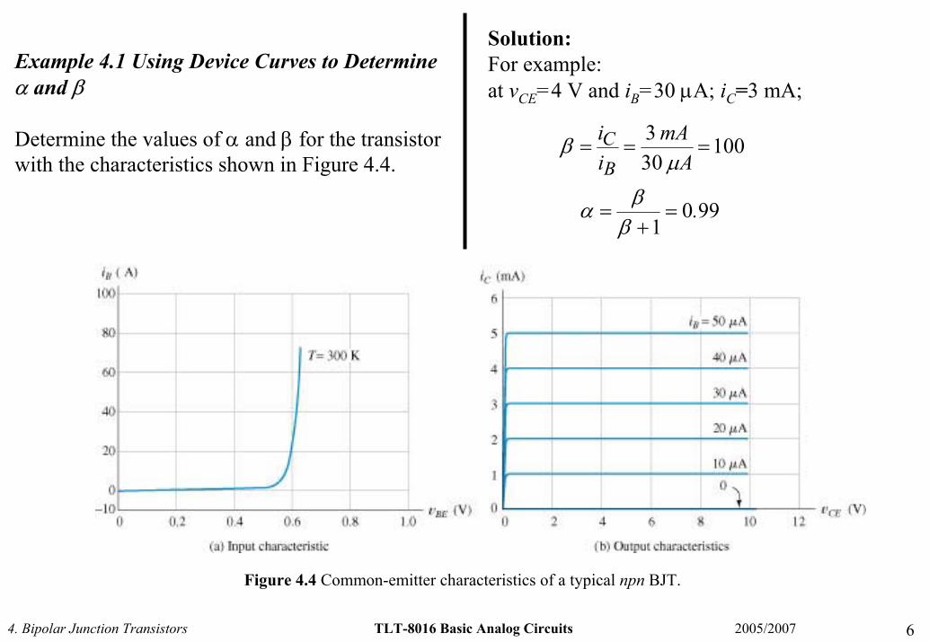
Solution:For example:at vCE=4 V and iB=30 µA; iC=3 mA;
Example 4.1 Using Device Curves to Determine α and β
Determine the values of α and β for the transistor with the characteristics shown in Figure 4.4.
100303
===A
mAiiBC
µβ
9901
.=+
=ββα
Figure 4.4 Common-emitter characteristics of a typical npn BJT.
4. Bipolar Junction Transistors TLT-8016 Basic Analog Circuits 2005/2007 7
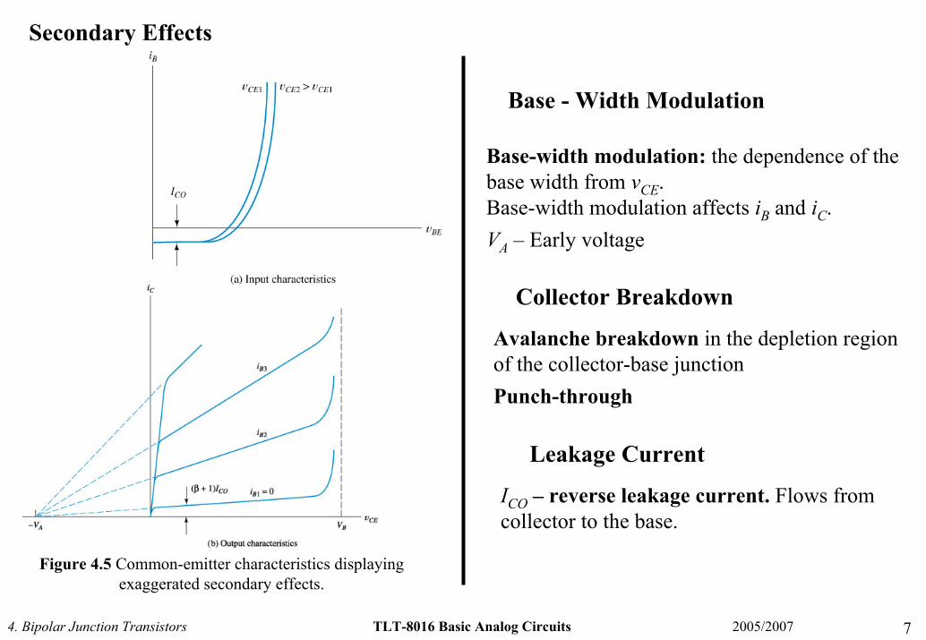
Secondary Effects
Base - Width Modulation
Base-width modulation: the dependence of the base width from vCE.Base-width modulation affects iB and iC.VA – Early voltage
Collector Breakdown
Avalanche breakdown in the depletion region of the collector-base junctionPunch-through
Leakage Current
ICO – reverse leakage current. Flows from collector to the base.
Figure 4.5 Common-emitter characteristics displaying exaggerated secondary effects.
4. Bipolar Junction Transistors TLT-8016 Basic Analog Circuits 2005/2007 8
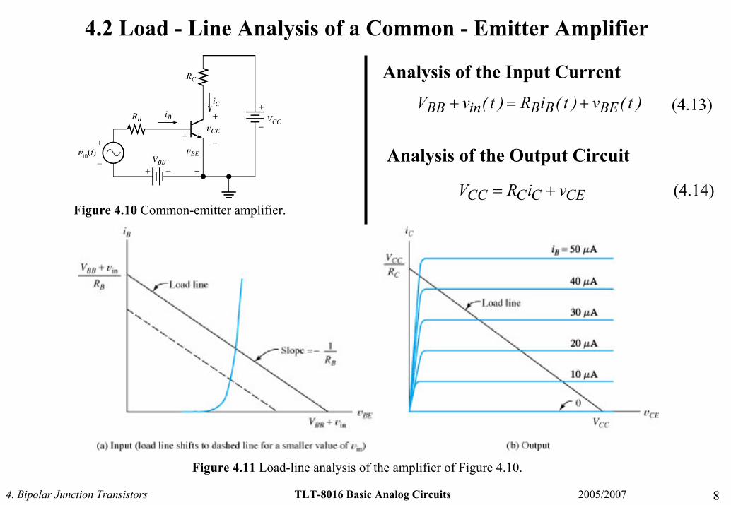
4.2 Load - Line Analysis of a Common - Emitter Amplifier
Figure 4.10 Common-emitter amplifier.
Analysis of the Input Current)t(v)t(iR)t(vV BEBBinBB +=+ (4.13)
Analysis of the Output Circuit
(4.14)CECCCC viRV +=
Figure 4.11 Load-line analysis of the amplifier of Figure 4.10.

4. Bipolar Junction Transistors TLT-8016 Basic Analog Circuits 2005/2007 9
Example 4.2 Graphical Determination of Q-point and Peak Signal SwingsSuppose that the current of Figure 4.10 has VCC=10 V, VBB=1.6 V, RB=40 kΩ and RC=2 kΩ. The input signal is a 0.4 V peak, 1 kHz sinusoid given by vin(t)=0.4sin(2000πt). The common-emitter characteristics for the transistor are shown in Figure 4.12a and b. Find the maximum, minimum and Q-point values for vCE.
Solution
Figure 4.12 Load-line analysis for Example 4.2.

4. Bipolar Junction Transistors TLT-8016 Basic Analog Circuits 2005/2007 10
Figure 4.13 Voltage waveforms for the amplifier of Figure 4.10. See Example 4.2.
Gain in Example 4.2:Amplitude at the input: 0.4VAmplitude at the output
7 – 5 = 2V
54.0
2==vA
4. Bipolar Junction Transistors TLT-8016 Basic Analog Circuits 2005/2007 11
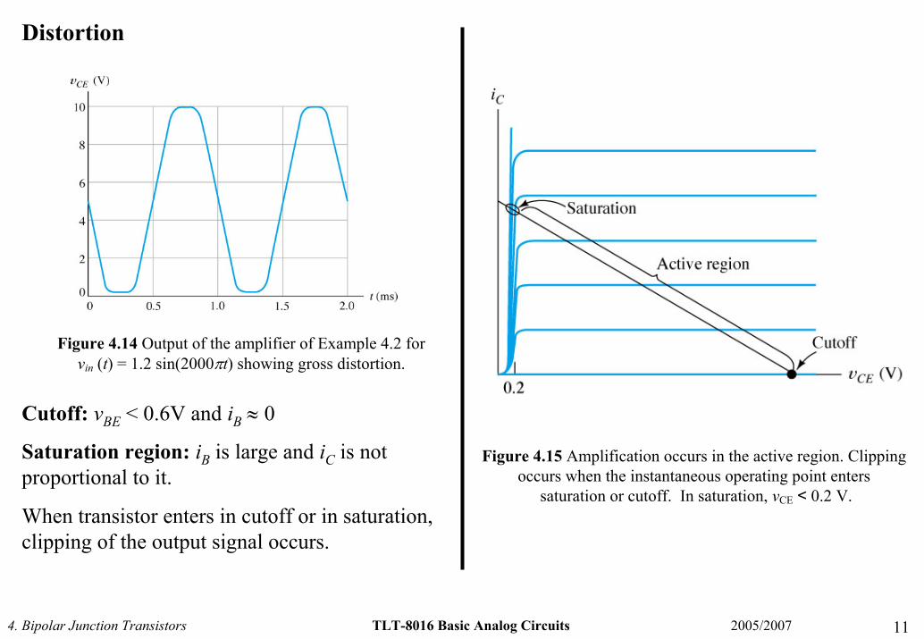
Distortion
Figure 4.14 Output of the amplifier of Example 4.2 for vin (t) = 1.2 sin(2000πt) showing gross distortion.
Cutoff: vBE < 0.6V and iB ≈ 0
Saturation region: iB is large and iC is not proportional to it.
When transistor enters in cutoff or in saturation, clipping of the output signal occurs.
Figure 4.15 Amplification occurs in the active region. Clipping occurs when the instantaneous operating point enters
saturation or cutoff. In saturation, vCE < 0.2 V.

4. Bipolar Junction Transistors TLT-8016 Basic Analog Circuits 2005/2007 12
4.3 The pnp Bipolar Junction Transistor
EC ii α=
( ) EB ii α−= 1
BC ii β=
BCE iii +=
−
−= 1
TBE
ESE VvexpIi
All relationships between the currents and voltages in a pnp BJT are the same as in npn BJT. There are two basic differences:• The currents flow in opposite directions;• The voltages have opposite polarities.
pnp transistor: thin n type semiconductor layer between two p type semiconductor layersBasic charge carriers: holes
(4.15)
(4.16)
(4.17)
(4.18)
(4.19)
Figure 4.16 The pnp BJT.

4. Bipolar Junction Transistors TLT-8016 Basic Analog Circuits 2005/2007 13
Figure 4.17 Common-emitter characteristics for a pnp BJT. Pay attention that the voltages are negative.

4. Bipolar Junction Transistors TLT-8016 Basic Analog Circuits 2005/2007 14
4.4 Large - Signal DC Circuit Models
Figure 4.20 Regions of operation on the characteristics of an npn BJT.
Active region: IB > 0; VCE > 0.2VSaturation region: IB > 0; βIB > IC > 0Cutoff region: VBE < 0.5V; VBC < 0.5V;

4. Bipolar Junction Transistors TLT-8016 Basic Analog Circuits 2005/2007 15
Active - Region Model
Figure 4.19a BJT large-signal models. (Note: Values shown are appropriate for typical small-signal silicon devices at a temperature of 300K.)

4. Bipolar Junction Transistors TLT-8016 Basic Analog Circuits 2005/2007 16
Saturation - Region Model
Figure 4.19b BJT large-signal models. (Note: Values shown are appropriate for typical small-signal silicon devices at a temperature of 300K.)
4. Bipolar Junction Transistors TLT-8016 Basic Analog Circuits 2005/2007 17
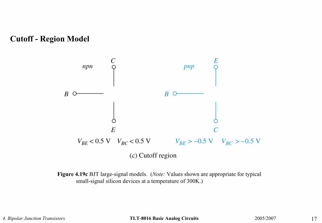
Cutoff - Region Model
Figure 4.19c BJT large-signal models. (Note: Values shown are appropriate for typical small-signal silicon devices at a temperature of 300K.)

4. Bipolar Junction Transistors TLT-8016 Basic Analog Circuits 2005/2007 18
Example 4.3 Determination of BJT Operation RegionA given transistor has β =100. Determine the region of operation if (a) IB = 50µA and IC = 3mA; (b) IB = 50µA and VCE = 5V; (c) VBE = -2V and VCE = -1V.
Solution:
(a) IB = 50µA > 0 – active or saturation region;βIB = 100×50×10-6 = 5mA > IC – saturation region.
(b) IB = 50µA > 0 – active or saturation region;VCE = 5V > 0.2V – active region.
(c) VBE = -2V < 0.5V – most probably cutoff;VCE = -1V < 0.5V – this confirms cutoff region.

4. Bipolar Junction Transistors TLT-8016 Basic Analog Circuits 2005/2007 19
4.5 Large - Signal DC Analysis of BJT Circuits
Step 1: Assume an operation region for the BJT and replace it by the corresponding large signal equivalent circuit.
Step 2: Solve the circuit to find IC, IB, and VCE.
Step 3: Check to see if the values found in Step 2 are consistent with the assumed operating state. If so the solution is complete; otherwise return to Step 1.

4. Bipolar Junction Transistors TLT-8016 Basic Analog Circuits 2005/2007 20
Solution:
First assumption: Cutoff. The equivalent circuit is in Figure 4.21(b).
IB = 0 – thus the voltage drop across RB is zero.Thus VBE = VCC = 15V > 0.5V.
The assumption is not valid.
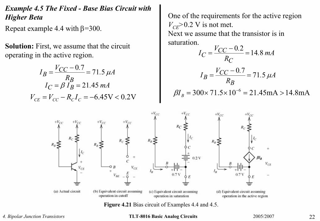
Example 4.4 The Fixed - Base Bias Circuit
The DC bias circuit shown in Figure 4.21a has RB=200 kΩ, RC=1 kΩ and VCC=15 V. The transistor has β = 100. Solve for IC and VCE.
Figure 4.21 Bias circuit of Examples 4.4 and 4.5.

4. Bipolar Junction Transistors TLT-8016 Basic Analog Circuits 2005/2007 21
Third assumption: Active region. The equivalent circuit is in Figure 4.21d.
Second assumption: Saturation. The equivalent circuit is in Figure 4.21c.
µA5.7110200
7.0157.03 =×
−=
−=
B
CCB R
VI
V85.71011015.715
mA15.733 =×××−=−=
==−
CCCCCE
BC
IRVV
II β
mA8.14101
2.0152.03 =
×−
=−
=C
CCC R
VI
µA5.7110200
7.0157.03 =×
−=
−=
B
CCB R
VI
βIB = 100×71.5×10-6 = 7.15mA < ICThe assumption is not valid.
IB > 0; VCE > 0.2V. The conditions are met.
Figure 4.21 Bias circuit of Examples 4.4 and 4.5.
4. Bipolar Junction Transistors TLT-8016 Basic Analog Circuits 2005/2007 22
Example 4.5 The Fixed - Base Bias Circuit with Higher BetaRepeat example 4.4 with β=300.
Solution: First, we assume that the circuit operating in the active region.
One of the requirements for the active region VCE>0.2 V is not met.Next we assume that the transistor is in saturation.
mA.R
.VIC
CCC 81420
=−
=
A.R
.VIB
CCB µ57170
=−
=
mA.II BC 4521== βA.
R.VI
BCC
B µ57170=
−=
14.8mAmA45.21105.71300 6 >=××= −BIβV2.0V45.6 <−=−= CCCCCE IRVV
Figure 4.21 Bias circuit of Examples 4.4 and 4.5.

4. Bipolar Junction Transistors TLT-8016 Basic Analog Circuits 2005/2007 23
Analysis for the Four - Resistor Bias Circuit
2121 11
1 R||RR/R/
RB =+
= (4.21)
CCB VRR
RV21
2+
= (4.22)
(4.23)EEBEBBB IRVIRV ++=
( ) BE II 1+= β
( ) EBBEB
B RRVVI
1++−
=β
(4.24)
(4.25)EECCCCCE IRIRVV −−=
Figure 4.28 Four-resistor bias circuit.
4. Bipolar Junction Transistors TLT-8016 Basic Analog Circuits 2005/2007 24
The principal goal of bias circuit design is to achieve nearly identical operating point for the BJTs, even though the BJT parameters may vary significantly from unit to unit.In the design usually are given the supply voltage VCC, the collector current IC in the quiescent point and often VCE in the quiescent point.The design steps are:1. Choice of VCE, if it is not specified. A good choice is
3CC
CEVV =
Discrete Bias - Circuit Design 5. Since IE = (β+1)IB ≈ IC
CEEEE IVIVR ≈=
6. VB = VE + VBE = VE + 0.7
( ) ( )( ) CCCCC
BBCC
B
IVVRIIVVR
IVR
−=+−=
=
21
227.
IB
I2
I2+IB
VB
VBE
+-
R2
R1 RC IC
VCC
+
-
IE
VCE
+
- VE
VC
RE
2. Determining of the voltage drop VE across REand the voltage VCC – VC, which is across RC. A good choice is
2CECC
CCCEVVVVV −
=−=
βCB II =3. Four-resistor bias circuit.
4. Choice of the current I2 to be I2 = (10..20)IB.

4. Bipolar Junction Transistors TLT-8016 Basic Analog Circuits 2005/2007 25
How the circuit stabilize the quiescent point?Assume that the emitter current IC is increased, due to some reason. Then• Emitter current IE is increased also, since IE ≈ IC.• VE increases since VE = IERE
• I2 is at least 10 times more than IB. It is the basic part of the current through R1. Thus the both currents are stable and depend very weak on the variation of the currents in the BJT.• The stable currents through R1 and R2 define a stable voltage VB. • VBE = VB - VE and the increasing of VE decreases VBE.• Smaller VBE means smaller base current IB (see the input characteristic in Figure 4.4).• IC = βIB and the smaller base current returns the collector current to its initial value.
IB
I2
I2+IB
VB
VBE
+-
R2
R1 RC IC
VCC
+
-
IE
VCE
+
- VE
VC
RE
Four-resistor bias circuit.
4. Bipolar Junction Transistors TLT-8016 Basic Analog Circuits 2005/2007 26
Problem D4.39. Four-resistor bias circuit design.Suppose that VCC = 20V, RC = 1kΩ, and a quiescent point of ICQ = 5mA is desired. The transistor has β ranging from 50 to 150. Design a four resistor bias circuit. Use standard 5%-tolerance resistors.Solution:Since RC is specified we can determine the voltage drop across it and the voltage VC
V2.87.05.7V5.72152
V15520
V5101105 33
=+=+=====
=−=
=×××==− −
BEEB
CCEE
C
CCQCCC
VVVVVV
V
RIVV
To determine IB, we take the smallest value of β. In this way we will determine the largest value of IB and the largest value of I2. If β is higher, the condition for I2 will be also satisfied.
( )( )
( ) ( )( ) ( ) kΩ7.10101001012.820
kΩ2.81012.8
15001055.7
6321
322
3
=×+×−=
+−==×==
Ω=×==
−−
−
−
BBCC
B
EEE
IIVVRIVR
IVR
The 5%-tolerance standard values for the resistors are RE = 1.5kΩ, R1 = 8.2kΩ, R2 = 11kΩ.
IB
I2
I2+IB
VB
VBE
+-
R2
R1 RC IC
VCC
+
-
IE
VCE
+
- VE
VC
RE
mA1101001010
µA100501056
2
3
=××==
=×==−
−
B
CB
II
II β Four-resistor bias circuit.
4. Bipolar Junction Transistors TLT-8016 Basic Analog Circuits 2005/2007 27
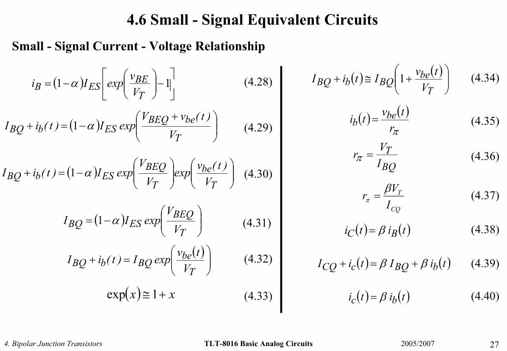
4.6 Small - Signal Equivalent CircuitsSmall - Signal Current - Voltage Relationship
( ) ( )
+≅+
Tbe
BQbBQ VtvItiI 1( )
−
−= 11
TBE
ESB VvexpIi α (4.34)(4.28)
( ) ( )πr
tvti beb =( )
+−=+
T
beBEQESbBQ V
)t(vVexpI)t(iI α1 (4.35)(4.29)
BQT
IVr =π (4.36)
( )
−=+
Tbe
T
BEQESbBQ V
)t(vexpV
VexpI)t(iI α1 (4.30)
CQ
T
IVr β
π = (4.37)
( )
−=
T
BEQESBQ V
VexpII α1 (4.31) ( ) ( )titi BC β= (4.38)
( )
=+
Tbe
BQbBQ VtvexpI)t(iI (4.32) ( ) ( )tiItiI bBQcCQ ββ +=+ (4.39)
( ) xx +≅1exp ( ) ( )titi bc β=(4.33) (4.40)
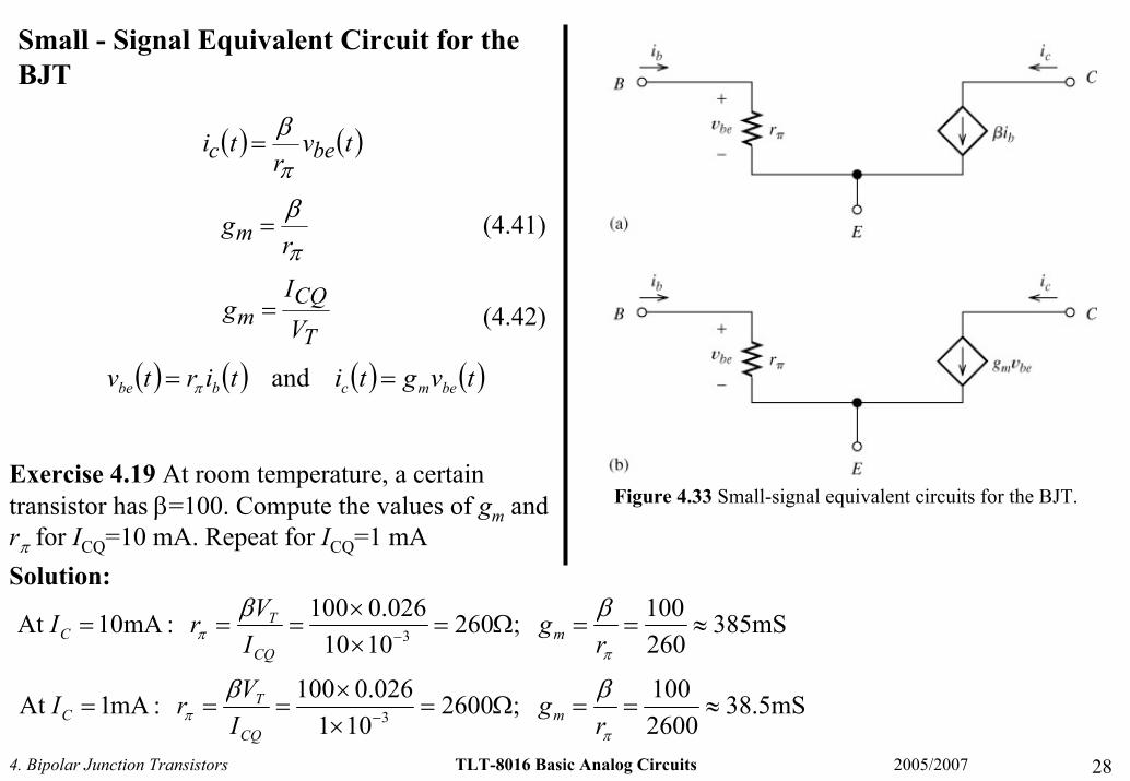
4. Bipolar Junction Transistors TLT-8016 Basic Analog Circuits 2005/2007 28
( ) ( )tvr
ti becπ
β=
π
βr
gm =
T
CQm V
Ig =
( ) ( ) ( ) ( )tvgtitirtv bemcbbe == andπ
Exercise 4.19 At room temperature, a certain transistor has β=100. Compute the values of gm and rπ for ICQ=10 mA. Repeat for ICQ=1 mASolution:
mS385260100 ;260
1010026.0100 :mA10At 3 ≈==Ω=
××
=== −π
πββr
gIVrI mCQ
TC
Small - Signal Equivalent Circuit for the BJT
(4.41)
(4.42)
Figure 4.33 Small-signal equivalent circuits for the BJT.
mS5.382600100 ;2600
101026.0100 :mA1At 3 ≈==Ω=
××
=== −π
πββr
gIVrI mCQ
TC

4. Bipolar Junction Transistors TLT-8016 Basic Analog Circuits 2005/2007 29
4.7 The Common - Emitter Amplifier
R1, R2, RC and RE1+RE2 form the four resistor biasing circuit;
C1 and C2 are coupling capacitors;
CE is bypass capacitor.
For ac signal the supply voltage is short circuit.
If RE1 = 0 the input signal is between the base and the emitter (ground); the output signal is between collector and the emitter (+VCC, which is ground for ac signal) –common-emitter amplifier.
Figure 4.34 Common-emitter amplifier.

4. Bipolar Junction Transistors TLT-8016 Basic Analog Circuits 2005/2007 30
The Small - Signal Equivalent Circuit
RE1
RE2 CE
RC RL
C2C1
R1 R2
Rs
vs
+
-
+
-
vin
+
-
voRE1 RC RL
R1 R2
Rs
vs
+
-
+
-
vin
+
-
vo
The second step in creating the small-signal equivalent circuit for mid-band region: the coupling capacitors and the bypass capacitors are replaced by short circuits
The first step in creating the small-signal equivalent circuit: the dc voltage sources are replaced by short circuits
Figure 4.34 Common-emitter amplifier. (b) Final small-signal mid-band equivalent circuit.

4. Bipolar Junction Transistors TLT-8016 Basic Analog Circuits 2005/2007 31
Voltage Gain
( ) bEb
Eebein
iRirRivv
11
1
++=+=
βπ(4.45)
b'Lo iRv β−= (4.46)
( ) 11 E
'L
ino
v RrR
vvA
++−==
ββ
π(4.47)
π
βrRA L
v
'
−=If RE1 = 0:
Figure 4.34 Common-emitter amplifier.
( ) 1
'
1
'
1 E
L
E
Lv R
RR
RA −≈+
−≅ββ
and the voltage gain doesn’t depend on BJT parameters.
If (β+1)RE1 >> rπ:Simplifications:
2121 11
1R/R/
R||RRB +== (4.43)
Open circuit voltage gain (when RL = ∞)
CLCL
'R/R/
R||RRL 111+
== (4.44)
( ) 11 EC
ino
vo RrR
vvA
++−==
ββ
π(4.48)

4. Bipolar Junction Transistors TLT-8016 Basic Analog Circuits 2005/2007 32
Input Impedance Current Gain and Power Gain
Lin
vino
i RZA
iiA == (4.51)
(4.52)vi AAG =
Figure 4.34 Common-emitter amplifier.
( ) 11 Ebin
it RrivZ ++== βπ (4.49)
itBinin
in Z/R/ivZ
111+
== (4.50)

4. Bipolar Junction Transistors TLT-8016 Basic Analog Circuits 2005/2007 33
Output Impedance
Figure 4.34 Common-emitter amplifier.
ib = 0 and βib = 0. Thus there is an open circuit between C and E.
(4.53)Co RZ =
4. Bipolar Junction Transistors TLT-8016 Basic Analog Circuits 2005/2007 34
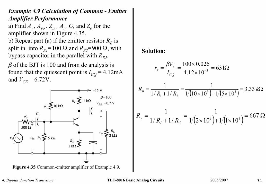
Example 4.9 Calculation of Common - Emitter Amplifier Performancea) Find Av , Avo , Zin , Ai , G, and Zo for the amplifier shown in Figure 4.35.b) Repeat part (a) if the emitter resistor RE is split in into RE1=100 Ω and RE2=900 Ω, with bypass capacitor in the parallel with RE2.β of the BJT is 100 and from dc analysis is found that the quiescent point is ICQ = 4.12mA and VCE = 6.72V.
Solution:
Ω=××
== − 6311012.4026.0100
3CQ
T
IVr β
π
( ) ( ) Ω=×+×
=+
= kRR
RB 33.3105110101
1/1/1
133
21
( ) ( ) Ω=×+×
=+
= 66710111021
1/1/1
133
'
CL RRR
L
Figure 4.35 Common-emitter amplifier of Example 4.9.

4. Bipolar Junction Transistors TLT-8016 Basic Analog Circuits 2005/2007 35
b)( )
( ) 21.61001100631
6671001 1
'
−=×++
×−=
++−==
E
L
in
ov Rr
RvvA
ββ
πa)
106631
667100'
−=×
−=−==π
βrR
vvA L
in
ov
( )
( ) 31.91001100631
101100
13
1
−=×++
××−=
++−==
E
C
in
ovo Rr
RvvA
ββ
π158
631101100 3
−=××
−=−==π
βrR
vvA C
in
ovo
Ω== 631πrZit
( ) ( ) Ω=×++=++== kRrivZ E
b
init 7.1010011006311 1βπ
( ) Ω=+×
=
+==
53163111033.31
1/1/1
1
3
itBin
inin ZRi
vZ
( ) ( ) Ω=×+×
=+
= kZR
ZitB
in 54.2107.1011033.31
1/1/1
133
89.7102
1054.221.6 3
3
−=××
−===L
inv
in
oi R
ZAiiA
1.28102
531106 3 −=×
−===L
inv
in
oi R
ZAiiA
( ) ( ) 0.4921.689.7 =−×−== vi AAG( ) ( ) 29801061.28 =−×−== vi AAG
Ω== k1Co RZkΩ1== Co RZ
4. Bipolar Junction Transistors TLT-8016 Basic Analog Circuits 2005/2007 36
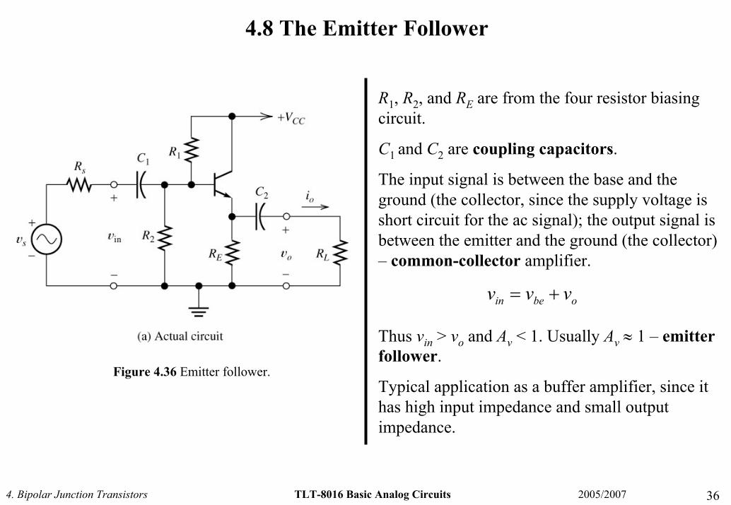
4.8 The Emitter Follower
R1, R2, and RE are from the four resistor biasing circuit.
C1 and C2 are coupling capacitors.
The input signal is between the base and the ground (the collector, since the supply voltage is short circuit for the ac signal); the output signal is between the emitter and the ground (the collector) – common-collector amplifier.
obein vvv +=
Thus vin > vo and Av < 1. Usually Av ≈ 1 – emitter follower.
Typical application as a buffer amplifier, since it has high input impedance and small output impedance.
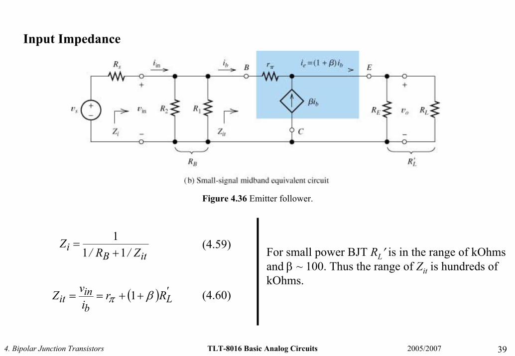
Figure 4.36 Emitter follower.

4. Bipolar Junction Transistors TLT-8016 Basic Analog Circuits 2005/2007 37
Small - Signal Equivalent Circuit
RE RLR1 R2
Rs
vs
+
-
+
-
vin
+
-
voRE RL
C2C1
R1 R2
Rs
vs
+
-
+
-
vin
+
-
vo
The second step in creating the small-signal equivalent circuit for mid-band region: the the coupling capacitors and the bypass capacitors are replaced by short circuits
The first step in creating the small-signal equivalent circuit: the dc voltage sources are replaced by short circuits
Figure 4.36 Emitter follower. (b) Final small-signal mid-band equivalent circuit.

4. Bipolar Junction Transistors TLT-8016 Basic Analog Circuits 2005/2007 38
Voltage Gain
Figure 4.36 Emitter follower.
( ) B'Lo iRv β+= 1 (4.56)Simplifications:
( ) 'Bbin LRiirv βπ ++= 1 (4.57)
2121 11
1R/R/
R||RRB +== (4.54)
( )( ) 11
1'
'
<++
+=
L
Lv Rr
RAβ
β
π
(4.58)
ELEL
'R/R/
R||RRL 111+
== (4.55)Since usually (1+β)RL′ >> rπ Av ≈ 1.
4. Bipolar Junction Transistors TLT-8016 Basic Analog Circuits 2005/2007 39
Input Impedance
Figure 4.36 Emitter follower.
itBi Z/R/
Z11
1+
= (4.59) For small power BJT RL′ is in the range of kOhmsand β ~ 100. Thus the range of Zit is hundreds of kOhms.
( ) 'L
bin
it RrivZ βπ ++== 1 (4.60)

4. Bipolar Junction Transistors TLT-8016 Basic Analog Circuits 2005/2007 40
Output Impedance
Figure 4.36 Emitter follower.
( ) ( ) ( )Esx
xo RrRi
vZ/1'/1
1+++
==πβ
xx
o ivZ = (4.65)(4.61)
( )βπ
++
=1
' rRZ sot
Ex
xbb Rviii =++ β (4.62) (4.66)
( ) mot g
rZ 11
≈+
≈β
πIf Rs′ ≈ 021
'
/1/1/11
RRRR
ss ++= (4.63)
For small power BJT gm ~ 102..103mS. Thus the range of Zot is Ohms or tens of Ohms.(4.64)0' =++ bsbx iRirv π

4. Bipolar Junction Transistors TLT-8016 Basic Analog Circuits 2005/2007 41
Example 4.10 Calculation of Emitter Follower Performance. Compute the voltage gain, input impedance, current gain, power gain, and output impedance of the emitter-follower amplifier displayed in Figure 4.37a.The dc analysis gives the following quiescent point: ICQ = 4.12mA and VCE = 11.7V.
( ) ( ) Ω=×+×
=+
= 66710211011
1/1/1
133
'
EL RRR
L
( )( )
( )( ) 991.0
667200112606672001
11
'
'
=×++
×+=
+++
=L
Lv Rr
RAβ
β
π
( ) ( ) Ω=×++=++= kRrZ Lit 135667200112601 'βπ
( ) ( ) Ω=×+×
=+
= kZR
ZitB
i 5.3610135110501
1/1/1
133
( ) ( ) ( ) Ω=×+×+×
=
++=
k
RRRR
ss
33.810100110100110101
1/1/1/1
1
333
21
'
( ) ( ) ( )
( ) ( ) ( ) Ω=×++×+
=
+++=
6.46102112601033.82001
1/1'/1
1
33
Eso RrR
ZπβFigure 4.37 Emitter follower of Example 4.10.
SolutionΩ=
××
== 12601012.4026.0200
3CQ
T
IVr β
π
( ) ( ) kΩ50101001101001
1/1/1
133
21
=×+×
=+
=RR
RB 8.38 ;2.36101
105.36991.0 3
3
===××
== ivL
ivi AAG
RZAA

4. Bipolar Junction Transistors TLT-8016 Basic Analog Circuits 2005/2007 42
4.9 The BJT as a Digital Logic Switch
Figure 4.41 RTL inverter.
The circuit in Fig. 4.41 is a modification of common-emitter amplifier intended for operation in saturation and in cut-off region only.Cut-off state: Vin < 0.5 (logical zero). BJT is in cut-off and IC = 0. There is no voltage drop across RC and Vo = +VCC (logical one).Saturation state: Vin is high (logical one), usually Vin ≈ +VCC.
B
inB R
Vi 7.0−=
C
CCC R
Vi 7.0−=
In saturation VCE < 0.2V. This Vo = VCE < 0.2V (logical zero).
To have saturation region, RB and RC must be designed in such a way that βiB > iC.
The output has logically opposite voltage to the input (zero-one; one-zero). The circuit is called logical inverter.Figure 4.42b Load-line analysis of RTL inverter under no-
load conditions.
4. Bipolar Junction Transistors TLT-8016 Basic Analog Circuits 2005/2007 43
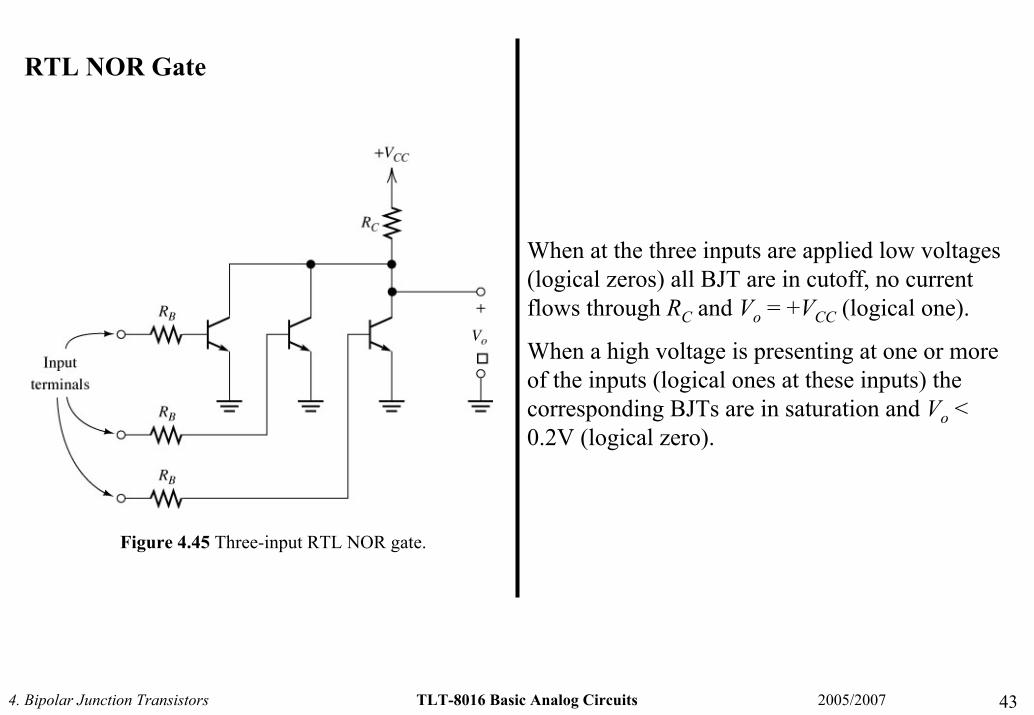
RTL NOR Gate
When at the three inputs are applied low voltages (logical zeros) all BJT are in cutoff, no current flows through RC and Vo = +VCC (logical one).
When a high voltage is presenting at one or more of the inputs (logical ones at these inputs) the corresponding BJTs are in saturation and Vo < 0.2V (logical zero).
Figure 4.45 Three-input RTL NOR gate.