34aa02/34lc02 data sheet - microchip
TRANSCRIPT

34AA02/34LC022K I2C™ Serial EEPROM Software Write-Protect
Features:
• Permanent and Resettable Software Write-Protect for Lower Half of the Array (00h-7Fh)
• Single Supply with Operation Down to 1.7V
• Low-Power CMOS Technology:
- Read current 1 mA, typical
- Standby current, 100 nA, typical
• 2-Wire Serial Interface Bus, I2C™ Compatible
• Cascadable up to Eight Devices
• Schmitt Trigger Inputs for Noise Suppression
• Output Slope Control to Eliminate Ground Bounce
• 100 kHz and 400 kHz Compatibility
• 1 MHz Clock for LC Versions
• Page Write Time 3 ms, typical
• Self-Timed Erase/Write Cycle
• 16-Byte Page Write Buffer
• ESD Protection > 4,000V
• Software Write Protection for Lower 128 Bytes
• Hardware Write Protection for Entire Array
• More than 1 Million Erase/Write Cycles
• Data Retention > 200 Years
• 8-Lead PDIP, SOIC, TSSOP, MSOP and TDFN Packages
• 6-Lead SOT-23 Package
• Pb-free and RoHS Compliant
• Available for Extended Temperature Ranges:
- Industrial (I): -40°C to +85°C
- Automotive (E): -40°C to +125°C
Device Selection Table
Package Types
Description:
The Microchip Technology Inc. 34AA02/34LC02(34XX02*) is a 2 Kbit Electrically Erasable PROMcapable of operation across a broad voltage range(1.7V to 5.5V). This device has two software write-protect features for the lower half of the array, as wellas an external pin that can be used to write-protect theentire array. This allows the system designer to protectnone, half, or all of the array, depending on theapplication. The device is organized as one block of256 x 8-bit memory with a 2-wire serial interface. Low-voltage design permits operation down to 1.7V, withstandby and active currents of only 100 nA and 1 mA,respectively. The 34XX02 also has a page writecapability for up to 16 bytes of data. The 34XX02 isavailable in the standard 8-pin PDIP, surface mountSOIC, TSSOP, MSOP and TDFN packages. The34XX02 is also available in the 6-lead, SOT-23package.Part
NumberVCC
RangeMax. Clock Frequency
Temp Ranges
34AA02 1.7-5.5 400 kHz(1) I,E
34LC02 2.2-5.5 1 MHz I,E
Note 1: 100 kHz for VCC <1.8V.
A0
A1
A2
VSS
1
2
3
4
8
7
6
5
VCC
WP
SCL
SDA
PDIP/SOIC/TSSOP/MSOP/TDFN
A0
A1
A2VSS
WP
SCL
SDA
VCC8
7
6
5
1
2
3
4
SOT-23
6
2
4SDA
VCC
VSS A0
A1
5
3
1SCL
*34XX02 is used in this document as a generic part numberfor the 34AA02/34LC02 devices.
2011 Microchip Technology Inc. DS22029F-page 1
34AA02/34LC02
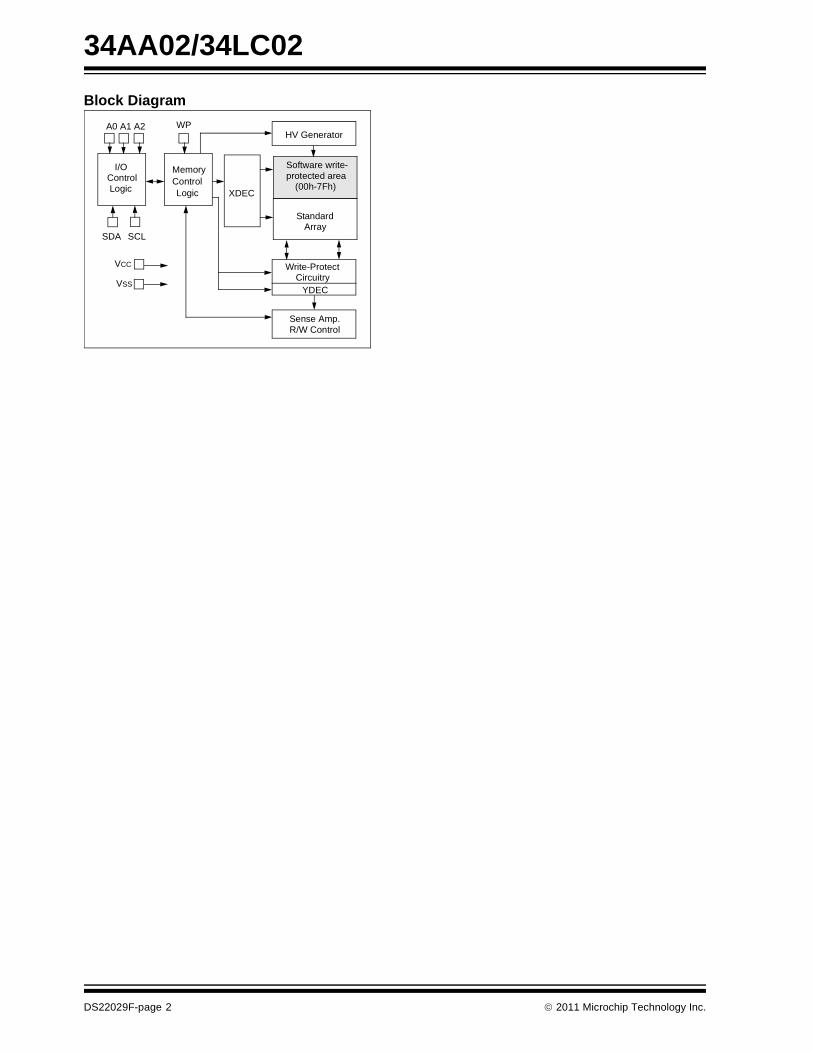
Block Diagram
I/OControl Logic
MemoryControl Logic XDEC
HV Generator
Standard Array
Software write-
Write-Protect Circuitry
YDEC
VCC
VSS
Sense Amp.R/W Control
SDA SCL
A0 A1 A2 WP
protected area(00h-7Fh)
DS22029F-page 2 2011 Microchip Technology Inc.

34AA02/34LC02
1.0 ELECTRICAL CHARACTERISTICS
Absolute Maximum Ratings(†)
VCC.............................................................................................................................................................................6.5V
All inputs and outputs w.r.t. VSS ..........................................................................................................-0.3V to VCC +1.0V
Storage temperature ............................................................................................................................... -65°C to +150°C
Ambient temperature with power applied................................................................................................-40°C to +125°C
ESD protection on all pins 4 kV
† NOTICE: Stresses above those listed under “Absolute Maximum Ratings” may cause permanent damage to thedevice. These are stress ratings only and functional operation of the device at these or any other conditions abovethose indicated in the operation sections of the specifications is not implied. Exposure to Absolute Maximum Ratingconditions for extended periods may affect device reliability.
TABLE 1-1: DC SPECIFICATIONS
DC CHARACTERISTICSVCC = +1.7V to +5.5VIndustrial (I): TA = -40°C to +85°CAutomotive (E):TA = -40°C to +125°C
Param.No.
Symbol Characteristic Min. Typ. Max. Units Conditions
— A0, A1, A2, SCL, SDA and WP pins
— — — — —
D1 VIH High-level input voltage 0.7 VCC — — V —
D2 VIL Low-level input voltage — — 0.3 VCC V 0.2 VCC for VCC < 2.5V
D3 VHYS Hysteresis of SchmittTrigger inputs
0.05 VCC — — V (Note)
D4 VOL Low-level output voltage — — 0.40 V IOL = 3.0 mA, VCC = 2.5V
D5 VHV High-Voltage Detect 7 — 10 V A0 Pin only, VCC < 2.2V
VCC + 4.8 — 10 V A0 Pin only, VCC 2.2V
10 — VCC + 4.8 V A0 Pin only, VCC 5.2V
D6 ILI Input leakage current — — ±1 A VIN = VSS or VCC
D7 ILO Output leakage current — — ±1 A VOUT = VSS or VCC
D8 CIN, COUT
Pin capacitance(all inputs/outputs)
— — 10 pF VCC = 5.5V (Note)TA = 25°C, FCLK = 1 MHz
D9 ICC write Operating current — 0.1 3 mA VCC = 5.5V, SCL = 1 MHz
D10 ICC read — 0.05 1 mA —
D11 ICCS Standby current ——
0.01—
15
AA
IndustrialAutomotiveSDA = SCL = VCC
A0, A1, A2, WP = VSS
Note: This parameter is periodically sampled and not 100% tested.
2011 Microchip Technology Inc. DS22029F-page 3

34AA02/34LC02
TABLE 1-2: AC SPECIFICATIONS
AC CHARACTERISTICSVCC = +1.7V to +5.5VIndustrial (I): TA = -40°C to +85°CAutomotive (E):TA = -40°C to +125°C
Param.No.
Symbol Characteristic Min. Max. Units Conditions
1 FCLK Clock frequency ———
100400
1000
kHz 1.7V VCC < 1.8V1.8V VCC 5.5V2.5V VCC 5.5V (34LC02)
2 THIGH Clock high time 4000600500
———
ns 1.7V VCC < 1.8V1.8V VCC 5.5V2.5V VCC 5.5V (34LC02)
3 TLOW Clock low time 47001300500
———
ns 1.7V VCC < 1.8V1.8V VCC 5.5V2.5V VCC 5.5V (34LC02)
4 TR SDA and SCL rise time (Note 1) ———
1000300300
ns 1.7V VCC < 1.8V1.8V VCC 5.5V2.5V VCC 5.5V (34LC02)
5 TF SDA and SCL fall time (Note 1) ———
1000300300
ns 1.7V VCC < 1.8V1.8V VCC 5.5V2.5V VCC 5.5V (34LC02)
6 THD:STA Start condition hold time 4000600250
———
ns 1.7V VCC < 1.8V1.8V VCC 5.5V2.5V VCC 5.5V (34LC02)
7 TSU:STA Start condition setup time 4700600250
———
ns 1.7V VCC < 1.8V1.8V VCC 5.5V2.5V VCC 5.5V (34LC02)
8 THD:DAT Data input hold time 0 — ns (Note 2)
9 TSU:DAT Data input setup time 250100100
———
ns 1.7V VCC < 1.8V1.8V VCC 5.5V2.5V VCC 5.5V (34LC02)
10 TSU:STO Stop condition setup time 4000600250
———
ns 1.7V VCC < 1.8V1.8V VCC 5.5V2.5V VCC 5.5V (34LC02)
11 TSU:WP WP setup time 4000600600
———
ns 1.7V VCC < 1.8V1.8V VCC 5.5V2.5V VCC 5.5V (34LC02)
12 THD:WP WP hold time 4700600600
———
ns 1.7V VCC < 1.8V1.8V VCC 5.5V2.5V VCC 5.5V (34LC02)
13 TAA Output valid from clock (Note 2) ———
3500900400
ns 1.7V VCC < 1.8V1.8V VCC 5.5V2.5V VCC 5.5V (34LC02)
14 TBUF Bus free time: Time the bus must be free before a new transmission can start
13004700
———
ns 1.7V VCC < 1.8V1.8V VCC 5.5V2.5V VCC 5.5V (34LC02)
16 TSP Input filter spike suppression(SDA and SCL pins)
— 50 ns All except 34LC02(Note 1 and Note 3)
17 TWC Write cycle time (byte or page) — 5 ms —
18 — Endurance 1M — cycles 25°C, VCC = 5.5V, Block mode (Note 4)
Note 1: Not 100% tested. CB = total capacitance of one bus line in pF.2: As a transmitter, the device must provide an internal minimum delay time to bridge the undefined region (minimum 300 ns) of the
falling edge of SCL to avoid unintended generation of Start or Stop conditions.3: The combined TSP and VHYS specifications are due to new Schmitt Trigger inputs, which provide improved noise spike suppres-
sion. This eliminates the need for a TI specification for standard operation.4: This parameter is not tested but ensured by characterization. For endurance estimates in a specific application, please consult
the Total Endurance™ Model which can be obtained from Microchip’s web site at www.microchip.com.
DS22029F-page 4 2011 Microchip Technology Inc.

34AA02/34LC02
FIGURE 1-1: BUS TIMING DATA
(unprotected)
(protected)
SCL
SDAIn
SDAOut
WP
5
7
6
16
3
2
8 9
13
D4 4
10
11 12
14
2011 Microchip Technology Inc. DS22029F-page 5

34AA02/34LC02
2.0 FUNCTIONAL DESCRIPTION
The 34XX02 has two Software Write-Protect featuresthat allow you to protect half of the array from beingwritten (Addresses 00h-7Fh). One command, SoftwareWrite-Protect (SWP) will prevent writes to half of thearray and is resettable by using the Clear SoftwareWrite-Protect (CSWP) command. The other commandis Permanent Software Write-Protect (PSWP), which isnot resettable and will permanently lock half the arrayfrom being written to. The device still has an externalpin (WP) that allows you to protect the entire array if sodesired.
The 34XX02 supports a bidirectional 2-wire bus anddata transmission protocol. A device that sends dataonto the bus is defined as a transmitter, and a devicereceiving data, as a receiver. The bus has to becontrolled by a master device, which generates theSerial Clock (SCL), controls the bus access and gener-ates the Start and Stop conditions, while the 34XX02works as slave. Both master and slave can operate astransmitter or receiver, but the master devicedetermines which mode is activated.
3.0 BUS CHARACTERISTICS
The following bus protocol has been defined:
• Data transfer may be initiated only when the bus is not busy.
• During data transfer, the data line must remain stable whenever the clock line is high. Changes in the data line while the clock line is high will be interpreted as a Start or Stop condition.
Accordingly, the following bus conditions have beendefined (Figure 3-1).
3.1 Bus Not Busy (A)
Both data and clock lines remain high.
3.2 Start Data Transfer (B)
A high-to-low transition of the SDA line while the clock(SCL) is high determines a Start condition. Allcommands must be preceded by a Start condition.
3.3 Stop Data Transfer (C)
A low-to-high transition of the SDA line while the clock(SCL) is high determines a Stop condition. Alloperations must be ended with a Stop condition.
3.4 Data Valid (D)
The state of the data line represents valid data when,after a Start condition, the data line is stable for theduration of the high period of the clock signal.
The data on the line must be changed during the lowperiod of the clock signal. There is one clock pulse perbit of data.
Each data transfer is initiated with a Start condition andterminated with a Stop condition. The number of databytes transferred between the Start and Stopconditions is determined by the master device and is,theoretically, unlimited; although only the last sixteenwill be stored when doing a write operation. When anoverwrite does occur, it will replace data in a first-in,first-out (FIFO) fashion.
3.5 Acknowledge
Each receiving device, when addressed, is obliged togenerate an Acknowledge after the reception of eachbyte. Exceptions to this rule relating to software writeprotection are described in Section 7.0 “Write Protec-tion”. The master device must generate an extra clockpulse, which is associated with this Acknowledge bit.
The device that acknowledges has to pull down theSDA line during the Acknowledge clock pulse in such away that the SDA line is stable low during the highperiod of the acknowledge related clock pulse. Ofcourse, setup and hold times must be taken intoaccount. During reads, a master must signal an end-of-data to the slave by not generating an Acknowledge biton the last byte that has been clocked out of the slave.In this case, the slave (34XX02) will leave the data linehigh to enable the master to generate the Stopcondition.
Note: The 34XX02 does not generate anyAcknowledge bits if an internalprogramming cycle is in progress.
DS22029F-page 6 2011 Microchip Technology Inc.

34AA02/34LC02
FIGURE 3-1: DATA TRANSFER SEQUENCE ON THE SERIAL BUS
3.6 Device Addressing
A control byte is the first byte received following theStart condition from the master device. The first part ofthe control byte consists of a 4-bit control code which isset to ‘1010’ for normal read and write operations and‘0110’ for writing to the write-protect register. Thecontrol byte is followed by three Chip Select bits (A2,A1, A0). The Chip Select bits allow the use of up toeight 34XX02 devices on the same bus and are used todetermine which device is accessed. The Chip Selectbits in the control byte must correspond to the logic lev-els on the corresponding A2, A1 and A0 pins for thedevice to respond.
For the SOT-23 package, the A2 pin is not connected.During device addressing, the A2 Chip Select bit(Figure 3-2) should be set to ‘0’. Only four 34XX02SOT-23 packages can be connected to the same bus.
The eighth bit of slave address determines if the masterdevice wants to read or write to the 34XX02(Figure 3-2). When set to a one, a read operation isselected. When set to a zero, a write operation isselected.
FIGURE 3-2: CONTROL BYTE ALLOCATION
4.0 WRITE OPERATIONS
4.1 Byte Write
Following the Start signal from the master, the devicecode(4 bits), the Chip Select bits (3 bits) and the R/Wbit, which is a logic low, are placed onto the bus by themaster transmitter. This indicates to the addressedslave receiver that a byte with a word address will follow,once it has generated an Acknowledge bit during theninth clock cycle. Therefore, the next byte transmittedby the master is the word address and will be writteninto the Address Pointer of the 34XX02.
After receiving another Acknowledge signal from the34XX02, the master device will transmit the data wordto be written into the addressed memory location. The34XX02 acknowledges again and the master generatesa Stop condition. This initiates the internal write cycle,which means that during this time, the 34XX02 will notgenerate Acknowledge signals (Figure 4-1). If anattempt is made to write to the array when the softwareor hardware write protection has been enabled, thedevice will acknowledge the command, but no data willbe written. The write cycle time must be observed evenif the write protection is enabled.
SCL
SDA
(A) (B) (D) (D) (A)(C)
StartCondition
Address orAcknowledge
Valid
DataAllowed
to Change
StopCondition
OperationControl Code
Chip Select
R/W
Read 1010 A2 A1 A0 1
Write 1010 A2 A1 A0 0
Write-Protect Register 0110 A2 A1 A0 0
OR
Start Read/Write
Slave Address R/W A
1 0 1 0 A2 A1 A0
0 1 1 0 A2 A1 A0
2011 Microchip Technology Inc. DS22029F-page 7

34AA02/34LC02
4.2 Page Write
The write control byte, word address and the first databyte are transmitted to the 34XX02 in the same way asin a byte write. Instead of generating a Stop condition,the master transmits up to 15 additional data bytes tothe 34XX02, which are temporarily stored in the on-chip page buffer and will be written into the memoryafter the master has transmitted a Stop condition. Uponreceipt of each word, the four lower order AddressPointer bits are internally incremented by one. Thehigher order four bits of the word address remainconstant. If the master should transmit more than 16bytes prior to generating the Stop condition, theaddress counter will roll over and the previouslyreceived data will be overwritten. As with the byte writeoperation, once the Stop condition is received, aninternal write cycle will begin (Figure 4-2). If an attemptis made to write to the array when the hardware writeprotection has been enabled, the device will acknowl-edge the command, but no data will be written. Thewrite cycle time must be observed even if the writeprotection is enabled.
FIGURE 4-1: BYTE WRITE
FIGURE 4-2: PAGE WRITE
Note: Page write operations are limited towriting bytes within a single physical page,regardless of the number of bytes actuallybeing written. Physical page boundariesstart at addresses that are integer multi-ples of the page buffer size (or ‘page size’)and end at addresses that are integer mul-tiples of [page size – 1]. If a Page Writecommand attempts to write across a phys-ical page boundary, the result is that thedata wraps around to the beginning of thecurrent page (overwriting data previouslystored there), instead of being written tothe next page, as might be expected. It istherefore necessary for the applicationsoftware to prevent page write operationsthat would attempt to cross a pageboundary.
S P
Bus ActivityMaster
SDA Line
Bus Activity
START
STOP
ControlByte
WordAddress Data
ACK
ACK
ACK
S P
Bus ActivityMaster
SDA Line
Bus Activity
START
ControlByte
WordAddress (n) Data (n) Data (n + 15)
STOP
ACK
ACK
ACK
ACK
ACK
Data (n + 1)
DS22029F-page 8 2011 Microchip Technology Inc.

34AA02/34LC02
5.0 ACKNOWLEDGE POLLING
Since the device will not acknowledge during a writecycle, this can be used to determine when the cycle iscomplete (this feature can be used to maximize busthroughput). Once the Stop condition for a Writecommand has been issued from the master, the deviceinitiates the internally timed write cycle. ACK pollingcan be initiated immediately. This involves the mastersending a Start condition followed by the control bytefor a Write command (R/W = 0). If the device is stillbusy with the write cycle, then no ACK will be returned.If the cycle is complete, then the device will return theACK and the master can then proceed with the nextRead or Write command. See Figure 5-1 for flowdiagram.
FIGURE 5-1: ACKNOWLEDGE POLLING FLOW
SendWrite Command
Send StopCondition to
Initiate Write Cycle
Send Start
Send Control Bytewith R/W = 0
Did DeviceAcknowledge(ACK = 0)?
NextOperation
No
Yes
2011 Microchip Technology Inc. DS22029F-page 9

34AA02/34LC02
6.0 READ OPERATION
Read operations are initiated in the same way as writeoperations, with the exception that the R/W bit of theslave address is set to ‘1’. There are three basic typesof read operations: current address read, random readand sequential read.
6.1 Current Address Read
The 34XX02 contains an address counter thatmaintains the address of the last word accessed, inter-nally incremented by ‘1’. Therefore, if the previousaccess (either a read or write operation) was toaddress n, the next current address read operationwould access data from address n+1. Upon receipt ofthe slave address with R/W bit set to ‘1’, the 34XX02issues an acknowledge and transmits the 8-bit dataword. The master will not acknowledge the transfer, butdoes generate a Stop condition and the 34XX02discontinues transmission (Figure 6-1).
6.2 Random Read
Random read operations allow the master to accessany memory location in a random manner. To performthis type of read operation, the word address must firstbe set. This is done by sending the word address to the34XX02 as part of a write operation. Once the wordaddress is sent, the master generates a Start conditionfollowing the acknowledge. This terminates the writeoperation, but not before the internal Address Pointer isset. The master then issues the control byte again, butwith the R/W bit set to a ‘1’. The 34XX02 then issuesan acknowledge and transmits the 8-bit data word. Themaster will not acknowledge the transfer, but doesgenerate a Stop condition and the 34XX02discontinues transmission (Figure 6-2).
6.3 Sequential Read
Sequential reads are initiated in the same way as arandom read, with the exception that after the 34XX02transmits the first data byte, the master issues acknowl-edge, as opposed to a Stop condition in a random read.This directs the 34XX02 to transmit the next sequen-tially addressed 8-bit word (Figure 6-3).
To provide sequential reads, the 34XX02 contains aninternal Address Pointer, which is incremented by oneat the completion of each operation. This AddressPointer allows the entire memory contents to be seriallyread during one operation.
6.4 Contiguous Addressing Across Multiple Devices
The Chip Select bits (A2, A1, A0) can be used toexpand the contiguous address space for up to 16K bitsby adding up to eight 34XX02 devices on the samebus. In this case, software can use A0 of the controlbyte as address bit A8; A1 as address bit A9, and A2as address bit A10. It is not possible to sequentiallyread across device boundaries.
6.5 Noise Protection and Brown-Out
The 34XX02 employs a VCC threshold detector circuitwhich disables the internal erase/write logic if the VCC
is below 1.35V at nominal conditions.
The SCL and SDA inputs have Schmitt Trigger andfilter circuits which suppress noise spikes to assureproper device operation, even on a noisy bus.
FIGURE 6-1: CURRENT ADDRESS READ
S P
Bus ActivityMaster
SDA Line
Bus Activity
STOP
ControlByte Data (n)
ACK
NO ACK
START
DS22029F-page 10 2011 Microchip Technology Inc.

34AA02/34LC02
FIGURE 6-2: RANDOM READ
FIGURE 6-3: SEQUENTIAL READ
S PS
Bus ActivityMaster
SDA Line
Bus Activity
START
STOP
ControlByte
ACK
WordAddress (n)
ControlByte
START
Data (n)
ACK
ACK
NO
ACK
P
Bus ActivityMaster
SDA Line
Bus Activity
STOP
ControlByte
ACK
NO ACK
Data (n) Data (n + 1) Data (n + 2) Data (n + X)
ACK
ACK
ACK
2011 Microchip Technology Inc. DS22029F-page 11

34AA02/34LC02
7.0 WRITE PROTECTION
The 34XX02 has two software write-protect features(SWP and PSWP) that allows the lower half of the array(addresses 00h-7Fh) to be write-protected, as well asa WP pin that can be used to protect the entire array.The permanent software write-protect feature isenabled by sending the device a special command.Once this feature has been enabled, it cannot bereversed. The resettable software write-protect featureis also enabled by sending the device a specialcommand but can be reset by issuing another specialcommand. In addition to the software protect features,there is a WP pin that can be used to write-protect theentire array, regardless of whether the software write-protect register has been written or not.
Table 7-2 and Table 7-3 describe how the 34XX02 willacknowledge specific commands under variouscircumstances.
7.1 Hardware Write Protection
The WP pin allows the user to write-protect the entirearray (00-FF) when the pin is tied to VCC. If the pin istied to VSS the write protection is disabled.
7.2 Software Write Protection (SWP) and Clear Software Write Protection (CSWP)
In addition to hardware write-protect the 34XX02 hasan additional software write-protect feature that, whenset, protects the first 128 bytes (00-7Fh) of the arrayfrom being written.
Setting the software write protection is done by sendingthe SWP instruction. SWP can also then be cleared byissuing a CSWP instruction (see Figure 7-1).
These two instructions follow the same format as theBYTE WRITE instruction with the exception of theDevice Type Identifier, (typically ‘1010’, insteadchanges to ‘0110’). Once this identifier is recognizedby the device, the rest of the Byte Write command,address and data, are “don’t cares”. In addition to theidentifier, high voltage must be applied to the A0 pin ofthe device and specific levels must be present on A1and A2. See Table 7-1 for the available commands.
7.3 Permanent Software Write-Protect (PSWP)
The Permanent software write protection, or PSWP isanother instruction that may be used to permanentlyprotect the first 128 byte of the array. Once thiscommand is issued, the user will no longer have theability to clear this feature regardless of instruction,power cycling, or state of the WP pin. Also, once thisinstruction has been executed, the device will nolonger acknowledge the device identifier ‘0110’.
FIGURE 7-1: SOFTWARE WRITE PROTECTION FOR SWP, CSWP, PSWP, OR CPSWP
Bus ActivityMaster
SDA Line
Bus Activity
START
ControlByte
Address Byte Data
STOP
ACK
ACK
ACK
S 0 1 1 0 0A2
A1
A0 P
“Don’t Care” “Don’t Care”
DS22029F-page 12 2011 Microchip Technology Inc.

34AA02/34LC02
TABLE 7-2: ACKNOWLEDGE TABLE FOR WRITE OR WRITE PROTECTION WITH R/W = 0
TABLE 7-3: ACKNOWLEDGE TABLE FOR WRITE OR WRITE PROTECTION WITH R/W = 1
TABLE 7-1: SOFTWARE WRITE PROTECTION INSTRUCTION SET WP = 0Address Pins Device Type Identifier Chip Select Bits R/W
A2 A1 A0 B7 B6 B5 B4 B3 B2 B1 B0
SWP VSS VSS VHV 0 1 1 0 0 0 1 0
CSWP VSS VCC VHV 0 1 1 0 0 1 1 0
PSWP A2 A1 A0 0 1 1 0 A2 A1 A0 0
Read SWP VSS VSS VHV 0 1 1 0 0 0 1 1
Read CSWP VSS VCC VHV 0 1 1 0 0 1 1 1
Read PSWP A2 A1 A0 0 1 1 0 A2 A1 A0 1
1. A0 is used to detect VHV for the SWP and CSWP commands.
2. B3, B2 and B1 are compared to the A2, A1 and A0 external pins, respectively on the 34XX02.
StatusWrite-
ProtectInstruction ACK Address ACK Data Byte ACK
Write Cycle
Permanently Protected x
PSWP, SWP, CSWPNo Ack
Don’t CareNo Ack
Don’t Care No Ack No
PAGE or BYTE WRITE in lower 128
bytesAck Address Ack Data No Ack No
Protected with SWP
0
SWPNo Ack
Don’t CareNo Ack
Don’t Care No Ack No
CSWP Ack Don’t Care Ack Don’t Care Ack Yes
PSWP Ack Don’t Care Ack Don’t Care Ack Yes
PAGE or BYTE WRITE in lower 128
bytesAck Address Ack Data No Ack No
1
SWPNo Ack
Don’t CareNo Ack
Don’t Care No Ack No
CSWP Ack Don’t Care Ack Don’t Care No Ack No
PSWP Ack Don’t Care Ack Don’t Care No Ack No
PAGE or BYTE WRITE
Ack Address Ack Data No Ack No
Not Protected
0PSWP, SWP, or CSWP Ack Don’t Care Ack Don’t Care Ack Yes
PAGE or BYTE WRITE
Ack Address Ack Data Ack Yes
1PSWP, SWP, or CSWP Ack Don’t Care Ack Don’t Care No Ack No
PAGE or BYTE WRITE
Ack Address Ack Address No Ack No
Status Instruction ACK
Permanently Protected PSWP, SWP, CSWP No Ack
Protected with SWP
SWP No Ack
CSWP Ack
PSWP Ack
Not protected PSWP, SWP, CSWP Ack
2011 Microchip Technology Inc. DS22029F-page 13

34AA02/34LC02
8.0 PIN DESCRIPTIONS
The descriptions of the pins are listed in Table 8-1.
TABLE 8-1: PIN FUNCTION TABLE
8.1 A0, A1, A2
The levels on these inputs are compared with thecorresponding bits in the slave address. The chip isselected if the compare is true.
Up to eight 34XX02 devices (four for the SOT-23package) may be connected to the same bus by usingdifferent Chip Select bit combinations. These inputsmust be connected to either VSS or VCC.
The A0 pin is also used to detect VHV.
8.2 Serial Address/Data Input/Output (SDA)
This is a bidirectional pin used to transfer addressesand data into and data out of the device. It is an opendrain terminal. Therefore, the SDA bus requires a pull-up resistor to VCC (typical 10 k for 100 kHz, 2 k for400 kHz).
For normal data transfer, SDA is allowed to changeonly during SCL low. Changes during SCL high arereserved for indicating the Start and Stop conditions.
8.3 Serial Clock (SCL)
This input is used to synchronize the data transfer toand from the device.
8.4 Write-Protect (WP)
This is the hardware write-protect pin. It can be tied toVCC or VSS. If tied to VCC, the hardware write protectionis enabled. If the WP pin is tied to VSS, the hardwarewrite protection is disabled.
Symbol PDIP SOIC TSSOP MSOP TDFN SOT-23 Description
A0 1 1 1 1 1 5 Chip Address Input
A1 2 2 2 2 2 4 Chip Address Input
A2 3 3 3 3 3 NC Chip Address Input
VSS 4 4 4 4 4 2 Ground
SDA 5 5 5 5 5 3 Serial Address/Data I/O
SCL 6 6 6 6 6 1 Serial Clock
WP 7 7 7 7 7 NC Write-Protect Input
VCC 8 8 8 8 8 6 +1.7V to 5.5V Power Supply
DS22029F-page 14 2011 Microchip Technology Inc.
34AA02/34LC02
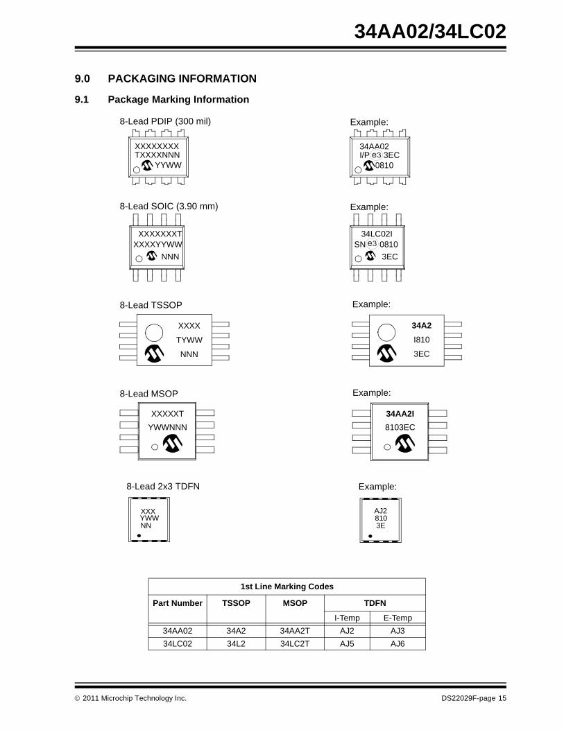
9.0 PACKAGING INFORMATION
9.1 Package Marking Information
XXXXXXXXTXXXXNNN
YYWW
8-Lead PDIP (300 mil) Example:
8-Lead SOIC (3.90 mm) Example:
XXXXXXXTXXXXYYWW
NNN
34AA02I/P 3EC
0810
34LC02ISN 0810
3EC
8-Lead MSOP Example:
XXXXXT
YWWNNN
34AA2I
8103EC
8-Lead TSSOP Example:
XXXX
TYWW
NNN
34A2
I810
3EC
8-Lead 2x3 TDFN
XXXYWWNN
Example:
3e
3e
AJ28103E
1st Line Marking Codes
Part Number TSSOP MSOP TDFN
I-Temp E-Temp
34AA02 34A2 34AA2T AJ2 AJ3
34LC02 34L2 34LC2T AJ5 AJ6
2011 Microchip Technology Inc. DS22029F-page 15

34AA02/34LC02
Example:6-Lead SOT-23
XXNN SKEC
SOT-23 Marking Codes
Device
34AA02
34LC02
I-Temp
SKNN
STNN
E-Temp
SLNN
SUNNPb-free topside mark is same; Pb-freenoted only on carton label.
Legend: XX...X Part number or part number codeT Temperature (I, E)Y Year code (last digit of calendar year)YY Year code (last 2 digits of calendar year)WW Week code (week of January 1 is week ‘01’)NNN Alphanumeric traceability code (2 characters for small packages)
Pb-free JEDEC designator for Matte Tin (Sn)
Note: For very small packages with no room for the Pb-free JEDEC designator , the marking will only appear on the outer carton or reel label.
Note: In the event the full Microchip part number cannot be marked on one line, it willbe carried over to the next line, thus limiting the number of availablecharacters for customer-specific information.
3e
3e
Note: Please visit www.microchip.com/Pbfree for the latest information on Pb-free conversion.
*Standard OTP marking consists of Microchip part number, year code, week code, and traceability code.
DS22029F-page 16 2011 Microchip Technology Inc.

34AA02/34LC02
���������� ���������� ������������� ����������
�������� ������ �!"�����#�$�%��&"��'��� ��(�)"&�'"!&�)�����&�#�*�&��&�����&���#������� +������%����&�,����&��!&���-� ��'��!��!�����#�.��#��&�����"#��'�#�%��!����&"!��!����#�%��!����&"!��!�!������&��$���#�����/����!�#���� ��'��!��������#�&���������������.�0������
1�,2�1�!�����'��!���� ���&��������$��&� ��"��!�*��*�&�"&�&������!�
����� 3�&���'!&��"��&����4����#�*���!(�����!��!���&��������������4�����������%���&������&�#��&��&&�255***�'��������'5���4�����
6��&! �7,8.���'��!���9�'�&! ��7 7:� ��;
7"')��%����! 7 <��&�� � �����1�, ��&����&��������� � = = ������#�#����4���� ���4��!! �� ���� ��-� ����1�!��&����&��������� �� ���� = =��"�#��&���"�#��>�#&� . ���� �-�� �-����#�#����4����>�#&� .� ���� ���� ��<�: �����9���&� � �-�< �-?� ���� ���&����&��������� 9 ���� ��-� ����9��#� ���4��!! � ���< ���� ����6����9��#�>�#&� )� ���� ��?� ����9*��9��#�>�#&� ) ���� ���< ����: ������*����������+ �1 = = ��-�
N
E1
NOTE 1
D
1 2 3
A
A1
A2
L
b1
b
e
E
eB
c
������� ������� ��*��� ,�����<1
2011 Microchip Technology Inc. DS22029F-page 17

34AA02/34LC02
Note: For the most current package drawings, please see the Microchip Packaging Specification located at http://www.microchip.com/packaging
DS22029F-page 18 2011 Microchip Technology Inc.

34AA02/34LC02
Note: For the most current package drawings, please see the Microchip Packaging Specification located at http://www.microchip.com/packaging
2011 Microchip Technology Inc. DS22029F-page 19

34AA02/34LC02
���������� �� ���!�� ���� �������""�#$��%&����������� !�'�
����� 3�&���'!&��"��&����4����#�*���!(�����!��!���&��������������4�����������%���&������&�#��&��&&�255***�'��������'5���4�����
DS22029F-page 20 2011 Microchip Technology Inc.

34AA02/34LC02
���������� ��() �� )" �*� ���!�� ���� (����+%+����������( !�
�������� ������ �!"�����#�$�%��&"��'��� ��(�)"&�'"!&�)�����&�#�*�&����&�����&���#������� ��'��!��!�����#�.��#��&�����"#��'�#�%��!����&"!��!����#�%��!����&"!��!�!������&��$���#������''����!�#��-� ��'��!��������#�&���������������.�0������
1�,2 1�!�����'��!���� ���&��������$��&� ��"��!�*��*�&�"&�&������!��.32 ��%��������'��!��(�"!"�����*�&�"&�&������(�%���%'�&����"�!�!�����
����� 3�&���'!&��"��&����4����#�*���!(�����!��!���&��������������4�����������%���&������&�#��&��&&�255***�'��������'5���4�����
6��&! ��99��. .����'��!���9�'�&! ��7 7:� ��;
7"')��%����! 7 <��&�� � ��?��1�,: �����8����& � = = ������#�#����4���� ���4��!! �� ��<� ���� �����&��#%%� �� ���� = ����: �����>�#&� . ?����1�,��#�#����4����>�#&� .� ��-� ���� ������#�#����4����9���&� � ���� -��� -���3&�9���&� 9 ���� ��?� ����3&���& 9� ������.33&������ � �R = <R9��#� ���4��!! � ���� = ����9��#�>�#&� ) ���� = ��-�
D
N
E
E1
NOTE 1
1 2
b
e
c
A
A1
A2
L1 L
φ
������� ������� ��*��� ,����<?1
2011 Microchip Technology Inc. DS22029F-page 21

34AA02/34LC02
Note: For the most current package drawings, please see the Microchip Packaging Specification located at
http://www.microchip.com/packaging
DS22029F-page 22 2011 Microchip Technology Inc.

34AA02/34LC02
���������� ��, �"�� ���!�� �����*�-���, ���, !�
�������� ������ �!"�����#�$�%��&"��'��� ��(�)"&�'"!&�)�����&�#�*�&����&�����&���#������� ��'��!��!�����#�.��#��&�����"#��'�#�%��!����&"!��!����#�%��!����&"!��!�!������&��$���#������''����!�#��-� ��'��!��������#�&���������������.�0������
1�,2 1�!�����'��!���� ���&��������$��&� ��"��!�*��*�&�"&�&������!��.32 ��%��������'��!��(�"!"�����*�&�"&�&������(�%���%'�&����"�!�!�����
����� 3�&���'!&��"��&����4����#�*���!(�����!��!���&��������������4�����������%���&������&�#��&��&&�255***�'��������'5���4�����
6��&! ��99��. .����'��!���9�'�&! ��7 7:� ��;
7"')��%����! 7 <��&�� � ��?��1�,: �����8����& � = = ������#�#����4���� ���4��!! �� ���� ��<� �����&��#%%� �� ���� = ����: �����>�#&� . �����1�,��#�#����4����>�#&� .� -����1�,: �����9���&� � -����1�,3&�9���&� 9 ���� ��?� ��<�3&���& 9� ������.33&������ � �R = <R9��#� ���4��!! � ���< = ���-9��#�>�#&� ) ���� = ����
D
N
E
E1
NOTE 1
1 2
e
b
A
A1
A2c
L1 L
φ
������� ������� ��*��� ,������1
2011 Microchip Technology Inc. DS22029F-page 23

34AA02/34LC02
Note: For the most current package drawings, please see the Microchip Packaging Specification located at
http://www.microchip.com/packaging
DS22029F-page 24 2011 Microchip Technology Inc.

34AA02/34LC02
Note: For the most current package drawings, please see the Microchip Packaging Specification located at
http://www.microchip.com/packaging
2011 Microchip Technology Inc. DS22029F-page 25
34AA02/34LC02
Note: For the most current package drawings, please see the Microchip Packaging Specification located at http://www.microchip.com/packaging
DS22029F-page 26 2011 Microchip Technology Inc.

34AA02/34LC02
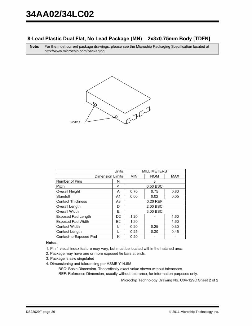
���������� ������.��$�����������*�-���,�����/0�0�%12����������(�.��
����� 3�&���'!&��"��&����4����#�*���!(�����!��!���&��������������4�����������%���&������&�#��&��&&�255***�'��������'5���4�����
2011 Microchip Technology Inc. DS22029F-page 27

34AA02/34LC02
3��������� �� ���!�� ���("��� ���"��!(��� !(�/��
�������� ��'��!��!�����#�.��#��&�����"#��'�#�%��!����&"!��!����#�%��!����&"!��!�!������&��$���#�������''����!�#���� ��'��!��������#�&���������������.�0������
1�,2 1�!�����'��!���� ���&��������$��&� ��"��!�*��*�&�"&�&������!�
����� 3�&���'!&��"��&����4����#�*���!(�����!��!���&��������������4�����������%���&������&�#��&��&&�255***�'��������'5���4�����
6��&! ��99��. .����'��!���9�'�&! ��7 7:� ��;
7"')��%����! 7 ?��&�� � �����1�,:"&!�#��9��#���&�� �� �����1�,: �����8����& � ���� = ������#�#����4���� ���4��!! �� ��<� = ��-��&��#%% �� ���� = ����: �����>�#&� . ���� = -�����#�#����4����>�#&� .� ��-� = ��<�: �����9���&� � ���� = -���3&�9���&� 9 ���� = ��?�3&���& 9� ��-� = ��<�3&������ � �R = -�R9��#� ���4��!! � ���< = ���?9��#�>�#&� ) ���� = ����
b
E
4N
E1
PIN 1 ID BYLASER MARK
D
1 2 3
e
e1
A
A1
A2 c
L
L1
φ
������� ������� ��*��� ,�����<1
DS22029F-page 28 2011 Microchip Technology Inc.

34AA02/34LC02
Note: For the most current package drawings, please see the Microchip Packaging Specification located at
http://www.microchip.com/packaging
2011 Microchip Technology Inc. DS22029F-page 29

34AA02/34LC02
APPENDIX A: REVISION HISTORY
Revision A (1/2007)
Original release of this document.
Revision B (2/2007)
Replaced Package Drawings.
Revision C (2/2008)
Added TDFN and SOT-23 Package info; Removed“VL” Part.
Revision D (4/2008)
Updated Product Identification System table, example (e).
Revision E (01/2010)
Revised SOT-23 and TDFN marking codes.
Revision F (03/2011)
Revised Section 3.6; Updated spec to new template.
DS22029F-page 30 2011 Microchip Technology Inc.

34AA02/34LC02
THE MICROCHIP WEB SITE
Microchip provides online support via our WWW site atwww.microchip.com. This web site is used as a meansto make files and information easily available tocustomers. Accessible by using your favorite Internetbrowser, the web site contains the followinginformation:
• Product Support – Data sheets and errata, application notes and sample programs, design resources, user’s guides and hardware support documents, latest software releases and archived software
• General Technical Support – Frequently Asked Questions (FAQ), technical support requests, online discussion groups, Microchip consultant program member listing
• Business of Microchip – Product selector and ordering guides, latest Microchip press releases, listing of seminars and events, listings of Microchip sales offices, distributors and factory representatives
CUSTOMER CHANGE NOTIFICATION SERVICE
Microchip’s customer notification service helps keepcustomers current on Microchip products. Subscriberswill receive e-mail notification whenever there arechanges, updates, revisions or errata related to aspecified product family or development tool of interest.
To register, access the Microchip web site atwww.microchip.com. Under “Support”, click on“Customer Change Notification” and follow theregistration instructions.
CUSTOMER SUPPORT
Users of Microchip products can receive assistancethrough several channels:
• Distributor or Representative
• Local Sales Office
• Field Application Engineer (FAE)
• Technical Support
• Development Systems Information Line
Customers should contact their distributor,representative or field application engineer (FAE) forsupport. Local sales offices are also available to helpcustomers. A listing of sales offices and locations isincluded in the back of this document.
Technical support is available through the web siteat: http://microchip.com/support
2011 Microchip Technology Inc. DS22029F-page 31

34AA02/34LC02
READER RESPONSE
It is our intention to provide you with the best documentation possible to ensure successful use of your Microchipproduct. If you wish to provide your comments on organization, clarity, subject matter, and ways in which ourdocumentation can better serve you, please FAX your comments to the Technical Publications Manager at(480) 792-4150.
Please list the following information, and use this outline to provide us with your comments about this document.
TO: Technical Publications Manager
RE: Reader ResponseTotal Pages Sent ________
From: Name
Company
Address
City / State / ZIP / Country
Telephone: (_______) _________ - _________
Application (optional):
Would you like a reply? Y N
Device: Literature Number:
Questions:
FAX: (______) _________ - _________
DS22029F34AA02/34LC02
1. What are the best features of this document?
2. How does this document meet your hardware and software development needs?
3. Do you find the organization of this document easy to follow? If not, why?
4. What additions to the document do you think would enhance the structure and subject?
5. What deletions from the document could be made without affecting the overall usefulness?
6. Is there any incorrect or misleading information (what and where)?
7. How would you improve this document?
DS22029F-page 32 2011 Microchip Technology Inc.
34AA02/34LC02
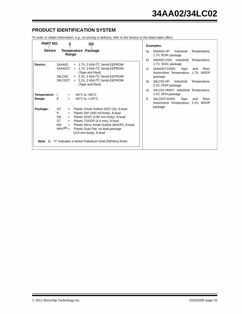
PRODUCT IDENTIFICATION SYSTEM
To order or obtain information, e.g., on pricing or delivery, refer to the factory or the listed sales office.
PART NO. X /XX
PackageTemperatureRange
Device
Device: 34AA02: = 1.7V, 2 Kbit I2C Serial EEPROM34AA02T: = 1.7V, 2 Kbit I2C Serial EEPROM
(Tape and Reel)34LC02: = 2.2V, 2 Kbit I2C Serial EEPROM34LC02T: = 2.2V, 2 Kbit I2C Serial EEPROM
(Tape and Reel)
TemperatureRange:
I = -40°C to +85°CE = -40°C to +125°C
Package: OT = Plastic Small Outline (SOT-23), 6-leadP = Plastic DIP (300 mil body), 8-leadSN = Plastic SOIC (3.90 mm body), 8-leadST = Plastic TSSOP (4.4 mm), 8-leadMS = Plastic Micro Small Outline (MSOP), 8-leadMNY(1) = Plastic Dual Flat, no lead package
(2x3 mm body), 8-lead
Examples:
a) 34AA02-I/P: Industrial Temperature,1.7V, PDIP package
b) 34AA02-I/SN: Industrial Temperature,1.7V, SOIC package
c) 34AA02T-E/MS: Tape and Reel,Automotive Temperature, 1.7V, MSOPpackage
d) 34LC02-I/P: Industrial Temperature,2.2V, PDIP package
e) 34LC02-I/MNY: Industrial Temperature,2.2V, DFN package
f) 34LC02T-E/MS: Tape and Reel,Automotive Temperature, 2.2V, MSOPpackage
Note 1: “Y” indicates a Nickel Palladium Gold (NiPdAu) finish.
2011 Microchip Technology Inc. DS22029F-page 33
34AA02/34LC02
NOTES:
DS22029F-page 34 2011 Microchip Technology Inc.

Note the following details of the code protection feature on Microchip devices:
• Microchip products meet the specification contained in their particular Microchip Data Sheet.
• Microchip believes that its family of products is one of the most secure families of its kind on the market today, when used in the intended manner and under normal conditions.
• There are dishonest and possibly illegal methods used to breach the code protection feature. All of these methods, to our knowledge, require using the Microchip products in a manner outside the operating specifications contained in Microchip’s Data Sheets. Most likely, the person doing so is engaged in theft of intellectual property.
• Microchip is willing to work with the customer who is concerned about the integrity of their code.
• Neither Microchip nor any other semiconductor manufacturer can guarantee the security of their code. Code protection does not mean that we are guaranteeing the product as “unbreakable.”
Code protection is constantly evolving. We at Microchip are committed to continuously improving the code protection features of ourproducts. Attempts to break Microchip’s code protection feature may be a violation of the Digital Millennium Copyright Act. If such actsallow unauthorized access to your software or other copyrighted work, you may have a right to sue for relief under that Act.
Information contained in this publication regarding deviceapplications and the like is provided only for your convenienceand may be superseded by updates. It is your responsibility toensure that your application meets with your specifications.MICROCHIP MAKES NO REPRESENTATIONS ORWARRANTIES OF ANY KIND WHETHER EXPRESS ORIMPLIED, WRITTEN OR ORAL, STATUTORY OROTHERWISE, RELATED TO THE INFORMATION,INCLUDING BUT NOT LIMITED TO ITS CONDITION,QUALITY, PERFORMANCE, MERCHANTABILITY ORFITNESS FOR PURPOSE. Microchip disclaims all liabilityarising from this information and its use. Use of Microchipdevices in life support and/or safety applications is entirely atthe buyer’s risk, and the buyer agrees to defend, indemnify andhold harmless Microchip from any and all damages, claims,suits, or expenses resulting from such use. No licenses areconveyed, implicitly or otherwise, under any Microchipintellectual property rights.
2011 Microchip Technology Inc.
Trademarks
The Microchip name and logo, the Microchip logo, dsPIC, KEELOQ, KEELOQ logo, MPLAB, PIC, PICmicro, PICSTART, PIC32 logo, rfPIC and UNI/O are registered trademarks of Microchip Technology Incorporated in the U.S.A. and other countries.
FilterLab, Hampshire, HI-TECH C, Linear Active Thermistor, MXDEV, MXLAB, SEEVAL and The Embedded Control Solutions Company are registered trademarks of Microchip Technology Incorporated in the U.S.A.
Analog-for-the-Digital Age, Application Maestro, CodeGuard, dsPICDEM, dsPICDEM.net, dsPICworks, dsSPEAK, ECAN, ECONOMONITOR, FanSense, HI-TIDE, In-Circuit Serial Programming, ICSP, Mindi, MiWi, MPASM, MPLAB Certified logo, MPLIB, MPLINK, mTouch, Omniscient Code Generation, PICC, PICC-18, PICDEM, PICDEM.net, PICkit, PICtail, REAL ICE, rfLAB, Select Mode, Total Endurance, TSHARC, UniWinDriver, WiperLock and ZENA are trademarks of Microchip Technology Incorporated in the U.S.A. and other countries.
SQTP is a service mark of Microchip Technology Incorporated in the U.S.A.
All other trademarks mentioned herein are property of their respective companies.
© 2011, Microchip Technology Incorporated, Printed in the U.S.A., All Rights Reserved.
Printed on recycled paper.
ISBN: 978-1-60932-947-1
DS22029F-page 35
Microchip received ISO/TS-16949:2002 certification for its worldwide headquarters, design and wafer fabrication facilities in Chandler and Tempe, Arizona; Gresham, Oregon and design centers in California and India. The Company’s quality system processes and procedures are for its PIC® MCUs and dsPIC® DSCs, KEELOQ® code hopping devices, Serial EEPROMs, microperipherals, nonvolatile memory and analog products. In addition, Microchip’s quality system for the design and manufacture of development systems is ISO 9001:2000 certified.

DS22029F-page 36 2011 Microchip Technology Inc.
AMERICASCorporate Office2355 West Chandler Blvd.Chandler, AZ 85224-6199Tel: 480-792-7200 Fax: 480-792-7277Technical Support: http://www.microchip.com/supportWeb Address: www.microchip.com
AtlantaDuluth, GA Tel: 678-957-9614 Fax: 678-957-1455
BostonWestborough, MA Tel: 774-760-0087 Fax: 774-760-0088
ChicagoItasca, IL Tel: 630-285-0071 Fax: 630-285-0075
ClevelandIndependence, OH Tel: 216-447-0464 Fax: 216-447-0643
DallasAddison, TX Tel: 972-818-7423 Fax: 972-818-2924
DetroitFarmington Hills, MI Tel: 248-538-2250Fax: 248-538-2260
IndianapolisNoblesville, IN Tel: 317-773-8323Fax: 317-773-5453
Los AngelesMission Viejo, CA Tel: 949-462-9523 Fax: 949-462-9608
Santa ClaraSanta Clara, CA Tel: 408-961-6444Fax: 408-961-6445
TorontoMississauga, Ontario, CanadaTel: 905-673-0699 Fax: 905-673-6509
ASIA/PACIFICAsia Pacific OfficeSuites 3707-14, 37th FloorTower 6, The GatewayHarbour City, KowloonHong KongTel: 852-2401-1200Fax: 852-2401-3431
Australia - SydneyTel: 61-2-9868-6733Fax: 61-2-9868-6755
China - BeijingTel: 86-10-8528-2100 Fax: 86-10-8528-2104
China - ChengduTel: 86-28-8665-5511Fax: 86-28-8665-7889
China - ChongqingTel: 86-23-8980-9588Fax: 86-23-8980-9500
China - Hong Kong SARTel: 852-2401-1200 Fax: 852-2401-3431
China - NanjingTel: 86-25-8473-2460Fax: 86-25-8473-2470
China - QingdaoTel: 86-532-8502-7355Fax: 86-532-8502-7205
China - ShanghaiTel: 86-21-5407-5533 Fax: 86-21-5407-5066
China - ShenyangTel: 86-24-2334-2829Fax: 86-24-2334-2393
China - ShenzhenTel: 86-755-8203-2660 Fax: 86-755-8203-1760
China - WuhanTel: 86-27-5980-5300Fax: 86-27-5980-5118
China - XianTel: 86-29-8833-7252Fax: 86-29-8833-7256
China - XiamenTel: 86-592-2388138 Fax: 86-592-2388130
China - ZhuhaiTel: 86-756-3210040 Fax: 86-756-3210049
ASIA/PACIFICIndia - BangaloreTel: 91-80-3090-4444 Fax: 91-80-3090-4123
India - New DelhiTel: 91-11-4160-8631Fax: 91-11-4160-8632
India - PuneTel: 91-20-2566-1512Fax: 91-20-2566-1513
Japan - YokohamaTel: 81-45-471- 6166 Fax: 81-45-471-6122
Korea - DaeguTel: 82-53-744-4301Fax: 82-53-744-4302
Korea - SeoulTel: 82-2-554-7200Fax: 82-2-558-5932 or 82-2-558-5934
Malaysia - Kuala LumpurTel: 60-3-6201-9857Fax: 60-3-6201-9859
Malaysia - PenangTel: 60-4-227-8870Fax: 60-4-227-4068
Philippines - ManilaTel: 63-2-634-9065Fax: 63-2-634-9069
SingaporeTel: 65-6334-8870Fax: 65-6334-8850
Taiwan - Hsin ChuTel: 886-3-6578-300Fax: 886-3-6578-370
Taiwan - KaohsiungTel: 886-7-213-7830Fax: 886-7-330-9305
Taiwan - TaipeiTel: 886-2-2500-6610 Fax: 886-2-2508-0102
Thailand - BangkokTel: 66-2-694-1351Fax: 66-2-694-1350
EUROPEAustria - WelsTel: 43-7242-2244-39Fax: 43-7242-2244-393Denmark - CopenhagenTel: 45-4450-2828 Fax: 45-4485-2829
France - ParisTel: 33-1-69-53-63-20 Fax: 33-1-69-30-90-79
Germany - MunichTel: 49-89-627-144-0 Fax: 49-89-627-144-44
Italy - Milan Tel: 39-0331-742611 Fax: 39-0331-466781
Netherlands - DrunenTel: 31-416-690399 Fax: 31-416-690340
Spain - MadridTel: 34-91-708-08-90Fax: 34-91-708-08-91
UK - WokinghamTel: 44-118-921-5869Fax: 44-118-921-5820
Worldwide Sales and Service
02/18/11