usb5537b data sheet - microchip technology
TRANSCRIPT

USB5537B7-Port SS/HS USB Hub Controller
General Description
The USB5537B hub is a 7-port SuperSpeed/Hi-Speed,low-power, configurable hub controller family fully com-pliant with the USB 3.0 Specification. The USB5537Bsupports 5 Gbps SuperSpeed (SS), 480 Mbps Hi-Speed (HS), 12 Mbps Full-Speed (FS) and 1.5 MbpsLow-Speed (LS) USB signaling for complete coverageof all defined USB operating speeds.
The USB5537B supports USB 2.0 speeds through itsUSB 2.0 hub controller. The new SuperSpeed hub con-troller (available on 4 of the 7 ports) operates in parallelwith the USB 2.0 controller, so the 5 Gbps SuperSpeeddata transfers are not affected by the slower USB 2.0traffic.
The USB5537B supports battery charging on a per portbasis. On battery charging enabled ports, the devicesprovide automatic USB data line handshaking. Thehandshaking supports USB 1.2 Charging DownstreamPort (CDP), Dedicated Charging Port (DCP) and non-USB 1.2 devices.
The USB5537B is configured for operation throughinternal default settings, where custom configurationsare supported through an on-chip OTP ROM, an exter-nal SPI ROM, or SMBus.
Product Features
• USB 3.0 compliant 5 Gbps, 480 Mbps, 12 Mbps and 1.5 Mbps operation, USB pins are 5 V toler-ant
- Integrated termination and pull-up/pull-down resistors
• Four downstream USB 3.0 ports
• Three additional USB 2.0 ports for use cases where SS is not required
• Supports battery charging of most popular battery powered devices
- USB-IF Battery Charging rev. 1.2 support (DCP & CDP)
- Apple Portable product charger emulation
- Blackberry charger emulation
- Chinese YD/T 1591-2006 charger emulation
- Chinese YD/T 1591-2009 charger emulation
- Supports additional portable devices
• Emulates portable/handheld native wall chargers
- Charging profiles emulate a handheld device’s wall charger to enable fast charging (minutes vs. hours)
• Enables charging from a mobile platform that is off
• Support tablets’ high current requirements
• Optimized for low-power operation and low ther-mal dissipation
• Vendor Specific Messaging (VSM) support for firmware upload over USB
• Configuration via OTP ROM, SPI ROM, or SMBus
• On-chip 8051 µC manages VBUS, and other hub signals
• 8 KB RAM, 32 KB ROM
• One Time programmable (OTP) ROM: 8 kbit
- Includes on-chip charge pump
• Single 25 MHz XTAL or clock input for all on-chip PLL and clocking requirements
• Supports JTAG boundary scan
• PHYBoost (USB 2.0)
- Selectable drive strength for improved signal integrity
• VariSense (USB 2.0)
- controls the receiver sensitivity enabling four programmable levels of USB signal receive sensitivity
• IETF RFC 4122 compliant 128-bit UUID
Software Features
• Compatible with Microsoft Windows 7, Vista, XP, Mac OSX10.4+, and Linux Hub Drivers
2012 - 2015 Microchip Technology Inc. DS00001682C-page 1

USB5537B
TO OUR VALUED CUSTOMERS
It is our intention to provide our valued customers with the best documentation possible to ensure successful use of your Microchipproducts. To this end, we will continue to improve our publications to better suit your needs. Our publications will be refined andenhanced as new volumes and updates are introduced.
If you have any questions or comments regarding this publication, please contact the Marketing Communications Department viaE-mail at [email protected]. We welcome your feedback.
Most Current Data SheetTo obtain the most up-to-date version of this data sheet, please register at our Worldwide Web site at:
http://www.microchip.com
You can determine the version of a data sheet by examining its literature number found on the bottom outside corner of any page. The last character of the literature number is the version number, (e.g., DS30000000A is version A of document DS30000000).
ErrataAn errata sheet, describing minor operational differences from the data sheet and recommended workarounds, may exist for cur-rent devices. As device/documentation issues become known to us, we will publish an errata sheet. The errata will specify therevision of silicon and revision of document to which it applies.
To determine if an errata sheet exists for a particular device, please check with one of the following:• Microchip’s Worldwide Web site; http://www.microchip.com• Your local Microchip sales office (see last page)
When contacting a sales office, please specify which device, revision of silicon and data sheet (include -literature number) you areusing.
Customer Notification SystemRegister on our web site at www.microchip.com to receive the most current information on all of our products.
DS00001682C-page 2 2012 - 2015 Microchip Technology Inc.

2012 - 2015 Microchip Technology Inc. DS00001682C-page 3
USB5537B
Table of Contents
1.0 Introduction ..................................................................................................................................................................................... 42.0 Block Diagram ................................................................................................................................................................................. 63.0 Pin Information ................................................................................................................................................................................ 74.0 Standard Interface Connections ................................................................................................................................................... 135.0 Functional Operation ..................................................................................................................................................................... 246.0 DC Parameters ............................................................................................................................................................................. 637.0 AC Specifications .......................................................................................................................................................................... 678.0 Package Drawing .......................................................................................................................................................................... 70Appendix A: Data Sheet Revision History ........................................................................................................................................... 72Appendix B: Acronyms ........................................................................................................................................................................ 74Appendix C: References ..................................................................................................................................................................... 75The Microchip Web Site ...................................................................................................................................................................... 76Customer Change Notification Service ............................................................................................................................................... 76Customer Support ............................................................................................................................................................................... 76Product Identification System ............................................................................................................................................................. 77

USB5537B
1.0 INTRODUCTION
1.1 Conventions
Within this manual, the following abbreviations and symbols are used to improve readability.
1.2 Overview
The USB5537B hub is a 7-port, low-power, configurable Hub Controller fully compliant with the USB 3.0 Specification2. The USB5537B supports 5 Gbps SuperSpeed (SS), 480 Mbps Hi-Speed (HS), 12 Mbps Full-Speed (FS) and1.5 Mbps Low-Speed (LS) USB signaling for complete coverage of all defined USB operating speeds.
All required resistors on the USB ports are integrated into the hub. This includes all series termination resistors and allrequired pull-down and pull-up resistors on D+ and D- pins. The over-current sense inputs for the downstream facingports have internal pull-up resistors.
The USB5537B hub includes programmable features such as:
• MultiTRAKTM Technology (USB 2.0): implements a dedicated Transaction Translator (TT) for each port. Dedi-cated TTs help maintain consistent full-speed data throughput regardless of the number of active downstream connections.
• PortSwap (USB 2.0): allows direct alignment of USB signals (D+/D-) to connectors to avoid uneven trace length or crossing of the USB differential signals on the PCB.
• PHYBoost (USB 2.0): enables 4 programmable levels of USB signal drive strength in downstream port transceiv-ers (HS, FS, LS USB only). PHYBoost will also attempt to restore USB signal integrity.
Example Description
BIT Name of a single bit within a field
FIELD.BIT Name of a single bit (BIT) in FIELD
x…y Range from x to y, inclusive
BITS[m:n] Groups of bits from m to n, inclusive
PIN Pin Name
zzzzb Binary number (value zzzz)
0xzzz Hexadecimal number (value zzz)
zzh Hexadecimal number (value zz)
rsvd Reserved memory location. Must write 0, read value indeterminate
code Instruction code, or API function or parameter
Multi Word NameUsed for multiple words that are considered a single unit, such as:Resource Allocate message, or Connection Label, or Decrement Stack Pointer instruction.
Section Name Section or Document name.
x Don’t care
<Parameter> <> indicate a Parameter is optional or is only used under some conditions
{,Parameter} Braces indicate Parameter(s) that repeat one or more times.
[Parameter]Brackets indicate a nested Parameter. This Parameter is not real and actually decodes into one or more real parameters.
DS00001682C-page 4 2012 - 2015 Microchip Technology Inc.

USB5537B
As shown on the Product Identification System page, three USB5537B firmware versions are available: “-5000”, “-6070”,and “-6080”. These options differ in the following ways:
• The Dynamic Charging Port feature and related DYNCPDIS_N pin function are only available on the -6070 and -6080 devices. Refer to Section 5.1.3, "Dynamic Charging Port (6070 and 6080 Only)" for additional details.
• The TRST/DYNCPDIS_N/UCS_SMBALERT_N pin buffer type is “IPU” in the -6070 and -6080 devices and “I” in the -5000 device. Refer to Pin Information on page 7 for additional details.
• The Global Suspend power consumption has been significantly lowered in the -6070 and -6080 device. Refer to Section 6.3, "Power Consumption" for additional details.
• The three USB 2.0 ports are configured as removable by default in the -6070 device. The three USB 2.0 ports are configured as non-removable by default in the -5000 and -6080 devices.
1.3 Configurable Features
The USB5537B hub controller provides a default configuration that is sufficient for most applications. When initializedin the default configuration, the following features may be configured:
• Downstream non-removable ports, where the hub will automatically report as a compound device
• Downstream disabled ports
• Downstream port power control and over-current detection on a ganged or individual basis
• USB signal drive strength
• USB differential pair pin location
The USB5537B hub controllers can alternatively be configured by OTP or as an SMBus slave device. When configuredby an OTP or over SMBus, the following configurable features are provided:
• Support for compound devices on a port-by-port basis
• Selectable over-current sensing and port power control on an individual or ganged basis to match the circuit board component selection
• Customizable vendor ID, product ID, and device ID
• Configurable delay time for filtering the over-current sense inputs
• Indication of the maximum current that the hub consumes from the USB upstream port
• Indication of the maximum current required for the hub controller
• Custom string descriptors (up to 30 characters): Product, manufacturer, and serial number
Note: At the time of this writing, products with a USB Host (or products such as docking stations with USB hubsthat must be submitted with an attached host enabled platform) are eligible for USB logo with a mixture ofUSB2.0 and USB3.0 ports. An example of such a product is a dedicated docking station that can only beused with a specific model or family of laptops. In this example, the docking station is submitted for USBlogo testing with a laptop and it is tested as a system. USB devices containing a hub with an exposedupstream port that can be plugged into any host platform through USB cables and connectors (examplesare USB enabled monitors, printers, hard drives, etc.) are not eligible for logo with a mixture of USB 3.0and USB 2.0 ports. These devices will need to consume the USB 2.0-only ports internally in order to beeligible for a USB logo.
2012 - 2015 Microchip Technology Inc. DS00001682C-page 5

USB5537B
DS00001682C-page 6 2012 - 2015 Microchip Technology Inc.
2.0 BLOCK DIAGRAM
FIGURE 2-1: USB5537B BLOCK DIAGRAM
US
B 3
.0 H
ub C
ontr
olle
r
TX
SS
PH
Y
RX
SS
PH
Y
US
B2.
0P
HY
US
B 2
.0 H
ub C
ontr
olle
r
Bu
ffer
HS
/FS
/LS
Ro
utin
g L
ogi
c
Com
mo
n B
lock
& P
LL
Reg
iste
rs
& H
ub I/
O
VB
US
Co
ntro
l
Bu
ffer
TX
SS
PH
Y
RX
SS
PH
Y
US
B2.
0P
HY
Bu
ffer
Bu
ffer
TX
SS
PH
Y
RX
SS
PH
Y
US
B2
.0P
HY
Bu
ffer
Buf
fer
TX
SS
PH
Y
RX
SS
PH
Y
US
B2.
0P
HY
Bu
ffer
Bu
ffer
TX
SS
PH
Y
RX
SS
PH
Y
US
B2.
0P
HY
Bu
ffer
Bu
ffer
Up
stre
am
US
B P
ort
Dow
nst
rea
m U
SB
Por
t 1D
owns
tre
am U
SB
Por
t 2D
owns
tre
am U
SB
Por
t 3D
ow
nstr
eam
US
B P
ort
4
Em
bed
ded
8051
µC
Re
gis
ters
&
Hu
b I/O
32
k R
OM
8k
RA
M
AP
B B
us
XD
ata
XD
ata
to
AP
B B
ridg
e
Dow
nstr
eam
RX
SS
bu
s
Dow
nst
rea
m T
X S
S b
us
Re
set
& 8
051
B
oot S
eq.
2k O
TP
SP
I M
ast
er
Tim
er
SP
I
US
B2
.0P
HY
Dow
nstr
eam
US
B 2
.0 P
ort
s 5,
6,
& 7
US
B2
.0P
HY
US
B2.
0P
HY

USB5537B
3.0 PIN INFORMATION
This chapter outlines the pinning configurations for each chip. The detailed pin descriptions are listed by function in Sec-tion 3.2, "Pin Descriptions (Grouped by Function)," on page 8.
3.1 Pin Configurations
FIGURE 3-1: USB5537B 72-PIN QFN
Ground Pad(must be connected to VSS with a via field)
USB5537B(Top View QFN-72)
US
B2D
P_D
N2
70
US
B3D
M_R
XD
N2
69
US
B3D
P_R
XD
N2
68
VD
D12
67
USB
3DM
_TX
DN
2
66
US
B3D
P_T
XD
N2
65
PR
T_P
WR
6/P
RT
_CT
L6
64
PR
T_P
WR
7/P
RT
_CT
L7
63
US
B2D
M_D
N1
62
US
B3D
M_R
XD
N1
60
US
B3D
P_R
XD
N1
59
VD
D12
58
USB
3DM
_TX
DN
1
57
US
B3D
P_T
XD
N1
56
55
US
B2D
P_D
N1
61
VD
D33
72
US
B2D
M_D
N2
71
USB2DM_DN5
16
USB2DP_DN5
15
USB2DM_DN4
14
USB2DP_DN4
13
USB3DM_RXDN412
USB3DP_RXDN4
11
VDD12
10
USB3DM_TXDN4
9
USB3DP_TXDN4
8
USB2DP_DN3
6
USB3DM_RXDN3
5
USB3DP_RXDN3
4
VDD12
3
USB3DM_TXDN3
2
USB3DP_TXDN3
1
USB2DM_DN3
7
TR
ST
/DY
NC
PD
IS_N
/U
CS
_SM
BA
LE
RT
_N
17
TC
K/O
CS
1
18
PR
T_P
WR
2/P
RT
_CT
L2
36
PR
T_P
WR
1/P
RT
_CT
L1
35
34
33
SP
I_D
I
32
SP
I_D
O
31
SP
I_C
LK
30
SP
I_C
E_N
29
VDD12
28
PR
T_P
WR
5/P
RT
_CT
L5/
SM
_DA
T
27
TE
ST
26
RE
SE
T_N
25
TD
I/O
CS
3
24
TD
O/O
CS
4
23
TM
S/O
CS
2
22
VD
D33
21
PRT_PWR4/PRT_CTL4
20
PR
T_P
WR
3/P
RT
_CT
L3
19
VDD33
54
RBIAS
53
XTALIN/CLK_IN
52
XTALOUT
51
USB3DM_RXUP
50
USB3DP_RXUP
49
VDD12
48
USB3DM_TXUP
47
USB3DP_TXUP
46
USB2DM_UP
45
USB2DP_UP
44
USB2DP_DN7
43USB2DM_DN7
42
USB2DP_DN6
41
USB2DM_DN6
40
VDD12
39
VB
US
38
VDD33
37
SM
_CL
K
ATEST
VD
D12
Indicates pins on the bottom of the device.
2012 - 2015 Microchip Technology Inc. DS00001682C-page 7

USB5537B
3.2 Pin Descriptions (Grouped by Function)
An N at the end of a signal name indicates that the active (asserted) state occurs when the signal is at a low voltagelevel. When the N is not present, the signal is asserted when it is at a high voltage level. The terms assertion and nega-tion are used exclusively in order to avoid confusion when working with a mixture of active low and active high signals.The term assert, or assertion, indicates that a signal is active, independent of whether that level is represented by a highor low voltage. The term negate, or negation, indicates that a signal is inactive.
TABLE 3-1: USB5537B PIN DESCRIPTIONS
Symbol Buffer Type Description
USB 3.0 INTERFACE
USB3DP_TXUP IO-U USB 3 Upstream
Upstream SuperSpeed transmit data plus
USB3DM_TXUP IO-U USB 3 Upstream
Upstream SuperSpeed transmit data minus
USB3DP_RXUP IO-U USB 3 Upstream
Upstream SuperSpeed receive data plus
USB3DM_RXUP IO-U USB 3 Upstream
Upstream SuperSpeed receive data minus
USB3DP_TXDN[4:1] IO-U USB 3 Downstream
Downstream SuperSpeed transmit data plus for ports 1 through 4.
USB3DM_TXDN[4:1] IO-U USB 3 Downstream
Downstream SuperSpeed transmit data minus for ports 1 through 4.
USB3DP_RXDN[4:1] IO-U USB 3 Downstream
Downstream SuperSpeed receive data plus for ports 1 through 4.
USB3DM_RXDN[4:1] IO-U USB 3 Downstream
Downstream SuperSpeed receive data minus for ports 1 through 4.
USB 2.0 INTERFACE
USB2DP_UPIO-U
USB Bus Data
These pins connect to the upstream USB bus data signals.
USB2DM_UPIO-U
USB Bus Data
These pins connect to the upstream USB bus data signals.
USB2DP_DN[7:1]IO-U
Hi-Speed USB Data
Downstream Hi-Speed data plus for ports 1 through 7.
USB2DM_DN[7:1]IO-U
Hi-Speed USB Data
Downstream Hi-Speed data minus for ports 1 through 7.
DS00001682C-page 8 2012 - 2015 Microchip Technology Inc.

USB5537B
USB PORT CONTROL
PRT_PWR[7:1]/PRT_CTL[7:1]
O12 USB Power Enable
Enables power to USB peripheral devices downstream.
Note: This pin also provides configuration strap functions. See Note 3-1.
VBUS I Upstream VBUS Power Detect
This pin can be used to detect the state of the upstream bus power. The device monitors this pin to determine when to assert the internal D+ pull-up resistor (signaling a connect event).
When designing a detachable hub, this pin should be connected to VBUS on the upstream port via a 2:1 voltage divider. Two 100 k resistors are suggested.
For self-powered applications with a permanently attached host, this pin must be connected to a dedicated host control output, or connected to the 3.3 V domain that powers the host (typically VDD33).
SPI INTERFACE
SPI_CE_N O12 SPI Enable
SPI_CLK O12 SPI Clock
SPI_DO
O12
SPI Serial Data Out
The output for the SPI port.
Note: This pin also provides configuration strap functions. See .
SPI_DI I SPI Serial Data In
The SPI data in to the controller from the ROM. This pin has a weak internal pull-down applied at all times to prevent floating.
JTAG/OCS INTERFACE
TRST
IPU(Note 3-4)
JTAG Asynchronous Reset
Note: If using the SMBus interface, a pull-up on this signal will enable Legacy Mode, while leaving it unconnected or pulled-down will enable Advanced Mode.
DYNCPDIS_N Dynamic Charging Port Disable
This active-low signal is used to globally disable charging port support.
Note: This signal available in -6070 and -6080 versions only
UCS_SMBALERT_N UCS1002 SMBus Alert
When charging port is enabled and SMBus devices are used, this signal acts as an active-low SMBus alert.
TCK
I
JTAG Clock
This input is used for JTAG boundary scan and has a weak pull-down. It can be left floating or grounded when not used. If the JTAG is connected, then this signal will be detected high, and the software disables the pull up after reset.
OCS1 Over-Current Sense 1
Input from external current monitor indicating an over-current condition.
Note: This pin also provides configuration strap functions. See Note 3-3.
TABLE 3-1: USB5537B PIN DESCRIPTIONS (CONTINUED)
Symbol Buffer Type Description
2012 - 2015 Microchip Technology Inc. DS00001682C-page 9

USB5537B
TMS
I
JTAG TMS
Used for JTAG boundary scan.
OCS2 Over-Current Sense 2
Input from external current monitor indicating an over-current condition.
Note: This pin also provides configuration strap functions. See Note 3-3.
TDI
I
JTAG TDI
Used for JTAG boundary scan.
OCS3 Over-Current Sense 3
Input from external current monitor indicating an over-current condition.
Note: This pin also provides configuration strap functions. See Note 3-3.
TDO
O12
JTAG TDO
Used for JTAG boundary scan.
OCS4 Over-Current Sense 4
Input from external current monitor indicating an over-current condition.
Note: This pin also provides configuration strap functions. See Note 3-3.
MISC
RESET_N IS Reset Input
The system uses this active low signal to reset the chip. The active low pulse should be at least 1 s wide.
XTALIN
ICLKx
Crystal Input: 25 MHz crystal.
This pin connects to either one terminal of the crystal or to an external 25 MHz clock when a crystal is not used.
CLK_IN External Clock Input
This pin connects to either one terminal of the crystal or to an external 25 MHz clock when a crystal is not used.
XTALOUT OCLKx Crystal Output
The clock output, providing a crystal 25 MHz. When an external clock source is used to drive XTALIN/CLKIN, this pin becomes a no connect.
TEST IPD Test Pin
Treat as a no connect pin or connect to ground. No trace or signal should be routed or attached to this pin.
RBIAS I-R USB Transceiver Bias
A12.0 k (+/- 1%) resistor is attached from ground to this pin to set the transceiver’s internal bias settings.
ATEST A Analog Test Pin
This signal is used for testing the chip and must always be connected to ground.
SM_CLK I/O12 SMBus Clock
SM_DAT I/O12 SMBus Data Pin
Note: This pin is MUXed with PRT_CTRL5
TABLE 3-1: USB5537B PIN DESCRIPTIONS (CONTINUED)
Symbol Buffer Type Description
DS00001682C-page 10 2012 - 2015 Microchip Technology Inc.

USB5537B
Note 3-1 The PRT_PWR[4:1] pins can optionally provide additional configuration strap functions toenable/disable the associated port and configure its battery charging capabilities. Configuration strapvalues are latched on device reset. Table 3-2 details the functions associated with the various strapsettings.
Strapping features are enabled by default and can be optionally disabled via the Pro-Touch softwareprogramming tool. For additional information on the Pro-Touch programming tool, contact your localsales representative.
Strapping functions are not supported for designs that support OCS but not power switching.
Note 3-2 The SPI_DO pin provides an additional SPI_SPD_SEL configuration strap function. SPI_SPD_SELselects between the 30MHz SPI Mode when pulled-down to ground (default) and the 60MHz SPIMode when pulled-up to VDD33. The SPI_SPD_SEL strap value is latched on Power-On Reset(POR) or RESET_N deassertion.
Note 3-3 The OCS[4:1] pins can optionally provide additional configuration strap functions. To set theassociated port into the non-removable state, the OCS pin must be configured with a pull-down(<10 k to VSS). Otherwise, the port will be configured in the removable state. Configuration strapvalues are latched on device reset.
Strapping features are enabled by default and can be optionally disabled via the Pro-Touch softwareprogramming tool. For additional information on the Pro-Touch programming tool, contact your localsales representative.
Strapping functions are not supported for designs that support OCS but not power switching.
Note 3-4 This pin has an internal pull-up only in the -6070 and -6080 versions. The internal pull-up is onlyactive after the SMBus mode (Legacy/Advanced) configuration strap has been sampled at POR orreset. The -5000 version is an “I” type buffer.
DIGITAL AND POWER (12 PINS AND 1 GROUND PAD)
(4) VDD33 3.3 V Power
(8) VDD12 1.25 V Power
VSS Ground Pad
This exposed pad is the device’s only connection to VSS and the primary thermal conduction path. Connect to an appropriate via field.
TABLE 3-2: PRT_PWR[4:1] CONFIGURATION STRAP STATES
PRT_PWR[4:1]Strap Setting
Port State Battery Charging
No Pull-Up or Pull-Down Enabled Disabled
Pull-Down:<10 k to VSS
Disabled N/A
Pull-Up:<10 kand >1 k to VDD33
Enabled Enabled
TABLE 3-1: USB5537B PIN DESCRIPTIONS (CONTINUED)
Symbol Buffer Type Description
2012 - 2015 Microchip Technology Inc. DS00001682C-page 11

USB5537B
3.3 Buffer Type Descriptions
TABLE 3-3: BUFFER TYPE DESCRIPTIONS
Buffer Type Description
I Input
I/O Input/output
IPD Input with internal weak pull-down resistor
IPU Input with internal weak pull-up resistor
IS Input with Schmitt trigger
O12 Output 12 mA
I/O12 Input/output buffer with 12 mA sink and 12 mA source
I/OSD12 Open drain with Schmitt trigger and 12 mA sink.
ICLKx XTAL clock input
OCLKx XTAL clock output
I-R RBIAS
I/O-U Analog input/output defined in USB specification
DS00001682C-page 12 2012 - 2015 Microchip Technology Inc.

USB5537B
4.0 STANDARD INTERFACE CONNECTIONS
4.1 SPI Interface
The hub will interface to external memory depending on configuration of the USB5537B pins associated with each inter-face type. The USB5537B will first check to see whether an external SPI Flash is present. If not, the USB5537B willoperate from internal ROM. If SPI Flash is present, the chip will operate from the external ROM.
The USB5537B is capable of code execution from an external SPI ROM. On power up, the firmware looks for an externalSPI flash device that contains a valid signature of 2DFU (device firmware upgrade) beginning at address 0xFFFA. If avalid signature is found, then the external ROM is enabled and the code execution begins at address 0x0000 in theexternal SPI device. If a valid signature is not found, then execution continues from internal ROM. The following sectionsdescribe the interface options to the external SPI ROM.
4.1.1 OPERATION OF THE HI-SPEED READ SEQUENCE
The SPI controller will automatically handle code reads going out to the SPI ROM Address. When the controller detectsa read, the controller drops the SPI_CE, and puts out a 0x0B, followed by the 24-bit address. The SPI controller thenputs out a DUMMY byte. The next eight clocks clock in the first byte. When the first byte is clocked in a ready signal issent back to the processor, and the processor gets one byte.
After the processor gets the first byte, its address will change. If the address is one more than the last address, the SPIcontroller will clock out one more byte. If the address in anything other than one more than the last address, the SPIcontroller will terminate the transaction by taking SPI_CE high. As long as the addresses are sequential, the SPI Con-troller will keep clocking in data.
FIGURE 4-1: SPI HI-SPEED READ OPERATION
SPICONTROLLER
SPIROM
Serial to Parllel
CE#
CLK
SI
SO
USB Hub
ADDRESSCONTROL
CACHE
SPI_DI
2012 - 2015 Microchip Technology Inc. DS00001682C-page 13

USB5537B
4.1.2 OPERATION OF THE DUAL HI-SPEED READ SEQUENCE
The SPI controller also supports dual data mode (at 30 MHz SPI speed only). When configured in dual mode, the SPIcontroller will automatically handle reads going out to the SPI ROM. When the controller detects a read, the controllerdrops the SPI_CE_N, and puts out a 0x3B, followed by the 24-bit address. The SPI controller then puts out a DUMMYbyte. The next four clocks clock in the first byte. The data appears two bits at a time on data out and data in. When thefirst byte is clocked in a ready signal is sent back to the processor, and the processor gets one byte.
After the processor gets the first byte, the address will change. If the address is one more than the last address, the SPIcontroller will clock out one more byte. If the address in anything other than one more than the last address, the SPIcontroller will terminate the transaction by taking SPI_CE_N high. As long as the addresses are sequential, the SPI Con-troller will keep clocking in data.
FIGURE 4-2: SPI HI-SPEED READ SEQUENCE
FIGURE 4-3: SPI DUAL HI-SPEED READ OPERATION
SPI_CEN
SPI_CLK
SPI_DO
SPI_DI
8
0B
MSB
HIGH IMPEDANCE
15 161 2 3 40 5 76
DOUT
ADD.
23 24
ADD. ADD. X
39 4031 32 47 48 55 56 63 64 71 72 80
DOUT
N N+1
DOUT
N+2
DOUT
N+3
DOUT
N+4
MSB
MSB
SPICONTROLLER
SPIROM
2-Serial to 8-Parallel
CE#
CLK
SI
SO
ADDRESSCONTROL
CACHE
SPI_DI
USB Hub
DS00001682C-page 14 2012 - 2015 Microchip Technology Inc.

USB5537B
4.1.3 32-BYTE CACHE
There is a 32-byte pipeline cache, and associated with the cache is a base address pointer and a length pointer. Oncethe SPI controller detects a jump, the base address pointer is initialized to that address. As each new sequential databyte is fetched, the data is written into the cache, and the length is incremented. If the sequential run exceeds 32 bytes,the base address pointer is incremented to indicate the last 32 bytes fetched. If the USB5537B does a jump, and thejump is in the cache address range, the fetch is done in 1 clock from the internal cache instead of an external access.
4.1.4 INTERFACE OPERATION TO SPI PORT WHEN NOT DOING FAST READS
There is an 8-byte command buffer: SPI_CMD_BUF[7:0]; an 8-byte response buffer: SPI_RESP_BUF[7:0]; and a lengthregister that counts out the number of bytes: SPI_CMD_LEN. Additionally, there is a self-clearing GO bit in the SPI_CTLRegister. Once the GO bit is set, the device drops SPI_CE_N, and starts clocking. It will put out SPI_CMD_LEN X 8 num-ber of clocks. After the first byte, the COMMAND, has been sent out, and the SPI_DI is stored in the SPI_RESP buffer.If the SPI_CMD_LEN is longer than the SPI_CMD_BUF, don’t cares are sent out on the SPI_DO line. This mode is usedfor program execution out of internal RAM or ROM.
FIGURE 4-4: SPI DUAL HI-SPEED READ SEQUENCE
FIGURE 4-5: SPI INTERNALLY-CONTROLLED OPERATION
SPI_CEN
SPI_CLK
SPI_DO
SPI_DI
8
0B
MSB
HIGH IMPEDANCE
15 161 2 3 40 5 76
D1
ADD.
23 24
ADD. ADD. X
39 4031 32 44 47 48 51 52 55 56 59
D2
N N+1
D3
N+2
D4
N+3
D5
N+4
MSB
MSB
D1 D2
N N+1
D3
N+2
D4
N+3
D5
N+4
MSB
43
Bits-7,5,3,1 Bits-7,5,3,1 Bits-7,5,3,1 Bits-7,5,3,1
Bits-6,4,2,0 Bits-6,4,2,0 Bits-6,4,2,0 Bits-6,4,2,0
Bits-7,5,3,1
Bits-6,4,2,0
SPICONTROLLER
SPIROM
SPI_RSP_BUF[7:0]
SPI_CMD_BUF[3:0]
SPI_CMD_LEN
CE#
CLK
SI
SO
USB Hub
2012 - 2015 Microchip Technology Inc. DS00001682C-page 15

USB5537B
4.1.4.1 ERASE EXAMPLE
To perform a SCTR_ERASE, 32BLK_ERASE, or 64BLK_ERASE, the device writes 0x20, 0x52, or 0xD8, respectivelyto the first byte of the command buffer, followed by a 3-byte address. The length of the transfer is set to 4 bytes. To dothis, the device first drops SPI_CE_N, then counts out 8 clocks. It then puts out the 8 bits of command, followed by 24bits of address of the location to be erased on the SPI_DO pin. When the transfer is complete, the SPI_CE_N goes high,while the SPI_DI line is ignored in this example.
4.1.4.2 BYTE PROGRAM EXAMPLE
To perform a Byte Program, the device writes 0x02 to the first byte of the command buffer, followed by a 3-byte addressof the location that will be written to, and one data byte. The length of the transfer is set to 5 bytes. The device first dropsSPI_CE_N, 8 bits of command are clocked out, followed by 24 bits of address, and one byte of data on the SPI_DO pin.The SPI_DI line is not used in this example.
FIGURE 4-6: SPI ERASE SEQUENCE
FIGURE 4-7: SPI BYTE PROGRAM
SPI_CEN
SPI_CLK
16 23 24 31151 2 3 40 5 76
ADD.
SPI_DO
SPI_DI
8
Command
MSB MSB
ADD. ADD.
HIGH IMPEDANCE
SPI_CEN
SPI_CLK
16 23 24 3115 391 2 3 40 5 76
0x00SPI_DO
SPI_DI
8
0xDB
MSB MSB
0xFE/0xFF
Data
MSB LSB
32
HIGH IMPEDANCE
0xBF
DS00001682C-page 16 2012 - 2015 Microchip Technology Inc.

USB5537B
4.1.4.3 COMMAND ONLY PROGRAM EXAMPLE
To perform a single byte command such as the following:
- - WRDI
- - WREN
- - EWSR
- - CHIP_ERASE
- - EBSY
- - DBSY
The device writes the opcode into the first byte of the SPI_CMD_BUF and the SPI_CMD_LEN is set to one. The devicefirst drops SPI_CE, then 8 bits of the command are clocked out on the SPI_DO pin. The SPI_DI is not used in this exam-ple.
4.1.4.4 JEDEC-ID READ EXAMPLE
To perform a JEDEC-ID command, the device writes 0x9F into the first byte of the SPI_CMD_BUF and the length of thetransfer is 4 bytes. The device first drops SPI_CE_N, then 8 bits of the command are clocked out, followed by the 24bits of dummy bytes (due to the length being set to 4) on the SPI_DO pin. When the transfer is complete, the SPI_CE_Ngoes high. After the first byte, the data on SPI_DI is clocked into the SPI_RSP_BUF. At the end of the command, thereare three valid bytes in the SPI_RSP_BUF. In this example, 0xBF, 0x25, 0x8E.
FIGURE 4-8: SPI COMMAND ONLY SEQUENCE
SPI_CEN
SPI_CLK
1 2 3 40 5 76
SPI_DO
SPI_DI
Command
MSB
HIGH IMPEDANCE
2012 - 2015 Microchip Technology Inc. DS00001682C-page 17

USB5537B
4.2 SMBus Slave Interface
Next, the USB5537B will look to receive configuration and commands from an optional SMBus master (if present). WhenSMBus is enabled, the SMBus can operate in either legacy (USB 2.0 only) or advanced mode (access to both USB 2.0and 3.0 registers). Next, the USB5537B will look for (optional) configuration present in the internal OTP memory. Anyregister settings that are modified via the SMBus interface will overwrite the internal OTP settings.
The SMBus slave interface is enabled when pull-up resistors are detected on both SM_DAT and SM_CLK for the firstmillisecond after reset. For operation in SMBus Legacy Mode, an additional pull-up resistor is required on TRST. If theSMBus interface is enabled, then the USB5537B will wait indefinitely for the SMBus host to configure the device. OnceSMBus configuration is complete, device initialization will proceed. To disable the SMBus, a pull-down resistor of 10 Kmust be applied to either SM_DAT, SM_CLK, or both SM_DAT and SM_CLK if desired. If SMBus is disabled, the deviceproceeds directly to device initialization using the internal OTP ROM.
4.2.1 PULL-UP RESISTOR FOR SMBUS
External pull-up resistors (10 k recommended) are required on the SM_DAT and SM_CLK pins when implementingeither SMBus mode.
FIGURE 4-9: SPI JEDEC-ID SEQUENCE
SPI_CEN
SPI_CLK
SPI_DO
SPI_DI
8
9F
MSB
HIGH IMPEDANCE
11 12 13 14 15 161 2 3 40 5 76 109 17 18 19 20 21 22 23 24 25 26 27 28 29 30 31 32 33 34
BF 25 8E
MSB MSB
DS00001682C-page 18 2012 - 2015 Microchip Technology Inc.

USB5537B
4.2.1.1 Invalid Protocol Response Behavior
Note that any attempt to update registers with an invalid protocol will not be updated. The only valid protocols are writeblock and read block (described Section 5.5, "SMBus Slave Interface," on page 29), where the hub only responds to the7-bit hardware selected slave addresses (0101100b or 0101101b). Additionally, the only valid registers for the hub areoutlined in the USB5537B Configuration Release Notes documentation.
4.2.2 SLAVE DEVICE TIMEOUT
Devices in a transfer can abort the transfer in progress and release the bus when any single clock low interval exceeds25 ms (TTIMEOUT, MIN). The master must detect this condition and generate a stop condition within or after the transferof the interrupted data byte. Slave devices must reset their communication and be able to receive a new START condi-tion no later than 35 ms (TTIMEOUT, MAX).
4.2.3 STRETCHING THE SCLK SIGNAL
The hub supports stretching of the SCLK by other devices on the SMBus. The hub will stretch the clock as needed.
4.2.4 BUS RESET SEQUENCE
The SMBus slave interface resets and returns to the idle state upon a START condition followed immediately by a STOPcondition.
4.2.5 SMBUS ALERT RESPONSE ADDRESS
The SMBALERT# signal is not supported by the USB5537B.
FIGURE 4-10: SMBUS SLAVE CONNECTION
Note: Some simple devices do not contain a clock low drive circuit; this simple kind of device typically resets itscommunications port after a start or stop condition. The slave device timeout must be implemented.
Master
SM_CLK
SM_DAT
SCL
SDA
VDD
10 k
USB Hub
10 k
2012 - 2015 Microchip Technology Inc. DS00001682C-page 19

USB5537B
4.3 Reset
There are two different resets that the device experiences. One is a hardware reset (either from the internal POR resetcircuit or via the RESET_N pin) and the second is a USB Bus Reset.
4.3.1 INTERNAL POR
All reset timing parameters are guaranteed by design.
4.3.2 EXTERNAL HARDWARE RESET
A valid hardware reset is defined as assertion of RESET_N for a minimum of 1 s after all power supplies are withinoperating range.
Assertion of RESET_N (external pin) causes the following:
1. The PHY is disabled, and the differential pairs will be in a high-impedance state.
2. All transactions immediately terminate; no states are saved.
3. All internal registers return to the default state.
4. The external crystal oscillator is halted.
5. The PLL is halted.
4.4 Standard Port Power Configuration
The device natively operates with standard port power controllers or poly-fuse devices for the downstream port powerswhen battery charging is not enabled on a port. It is not recommended to have the downstream ports of a single devicemix poly-fuse and standard power controller support, as the configuration of the hub cannot correctly report which portsare poly-fuse and which are port power controllers to the host.
Any port without battery charging can also be used in individual port power controls or ganged power controls. The portpower control output only supports either Ganged or Individual modes on a global basis for all downstream ports.
The overcurrent setting also supports individual or global settings, but also adds the ability to configure specific ports tobe part of an overcurrent gang with others setup for individual connections. This hybrid configuration should only beused when utilizing poly-fuse power devices.
4.4.1 PORT POWER CONTROLLER
The most common method for downstream port power controls is to utilize current-limited power switches for USB appli-cations. The devices allow the downstream port powers to be enabled through a control signal and report over-currentconditions through a flag output.
Two connection methods are possible for these controllers, Combined mode and Independent mode.
In Combined mode, the FLG and EN signals are tied together with an external 10K ohm pull-up and driven to a singlePRT_CTL signal on the device, as shown in Figure 4-11.
DS00001682C-page 20 2012 - 2015 Microchip Technology Inc.

USB5537B
In Individual mode, the PRT_CTL signal is driven directly to the EN input of the power switch and the OCS input is con-nected to the FLG output of the power switch with a 10K pull-up connected, as shown in Figure 4-12.
FIGURE 4-11: COMBINED MODE IMPLEMENTATION
FIGURE 4-12: INDIVIDUAL MODE IMPLEMENTATION
Note: Ports 1-4 have the option to be configured for either Combined mode or Individual mode, but ports 5-7 onlysupport Combined mode connections.
USB Power Switch
EN
OCS
5V
USB Device
PRT_CTL
USB553x
USB Power Switch
EN
5V
USB Device
PRT_CTL
FLGOCS
USB553x10k
5V
2012 - 2015 Microchip Technology Inc. DS00001682C-page 21

USB5537B
4.4.2 POLY-FUSE
An alternate method of downstream power control is to utilize poly-fuse devices. In this configuration, the poly-fusedevices are used to report overcurrent conditions to the USB5537B through the OCS input, as shown in Figure 4-13.
4.5 Charging Port Configurations
The device can also be configured to operate as a charging port for one or more downstream ports. Ganged port powercontrol and/or overcurrent is not supported if any of the downstream ports are configured as charging ports. If a port isconfigured to support a charging port mode, either a standard port power controller or a UCS1002 may be implemented.
For more information on charging port support, refer to Section 5.1, "Charging Port Configuration," on page 24.
4.5.1 PORT POWER CONTROLLER
The only special limitation of using the device as a charging port is that the port power controller must be capable of thehigher current to support the charging port modes. Refer to Section 4.4.1, "Port Power Controller," on page 20 for moreinformation on this implementation.
4.5.2 UCS1002
Using a UCS1002 device as a downstream port power controller is only supported on ports that are enabled as chargingports.
If the UCS1002 is implemented, the USB5537B communicates with all of the implemented UCS1002 ports over SMBususing one of the PRT_CTLx/OCSx signals as the SMCLK/SMDAT. Additionally, DYNCPDIS_N becomes the UCS_SM-BALERT_N signal. Multiple UCS1002 devices may be connected to the SMBus in parallel.
After reset, for any enabled charging ports, the USB5537B performs SMBus commands on the configuredPRT_CTLx/OCSx signals and checks UCS1002 devices at specific addresses (see Table 4-1) to confirm which portsare utilizing UCS1002 devices as the downstream power controllers.
FIGURE 4-13: POLY-FUSE IMPLEMENTATION
OCS
USB Device
5V
Poly Fuse
USB553x
10k
3.3V
DS00001682C-page 22 2012 - 2015 Microchip Technology Inc.
USB5537B
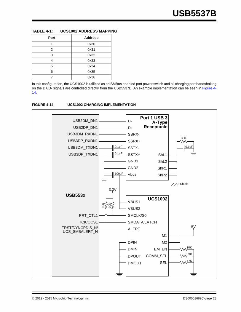
In this configuration, the UCS1002 is utilized as an SMBus enabled port power switch and all charging port handshakingon the D+/D- signals are controlled directly from the USB5537B. An example implementation can be seen in Figure 4-14.
TABLE 4-1: UCS1002 ADDRESS MAPPING
Port Address
1 0x30
2 0x31
3 0x32
4 0x33
5 0x34
6 0x35
7 0x36
FIGURE 4-14: UCS1002 CHARGING IMPLEMENTATION
D-
5V
USB553x
D+
USB2DM_DN1
USB2DP_DN1
SSRX-
SSRX+
USB3DM_RXDN1
USB3DP_RXDN1
SSTX-
SSTX+
USB3DM_TXDN1
USB3DP_TXDN1 0.1uF
0.1uF
GND1
GND2
Vbus100uF
ShL1
ShL2
ShR1
ShR2
0.1uF
Shield
Port 1 USB 3A-Type
Receptacle
330
VBUS1
VBUS2
SMCLK/S0
SMDATA/LATCH
ALERT
DPIN
M1
M2
UCS1002
PRT_CTL1
DMIN
DPOUT
DMOUT
EM_EN
COMM_SEL
SEL 47K
33K
10K
TRST/DYNCPDIS_N/UCS_SMBALERT_N
3.3V
10K
10K
TCK/OCS1
2012 - 2015 Microchip Technology Inc. DS00001682C-page 23

USB5537B
5.0 FUNCTIONAL OPERATION
This chapter details the functional operation of various device features.
5.1 Charging Port Configuration
The USB5537B supports downstream charging ports on any available port. The hub contains internal hardware andalgorithms to natively support various voltage levels on the D+/D- signals along with the BC 1.2 Handshaking protocol,allowing charging devices to detect the downstream port as a charging port.
A port can be configured for either RapidCharge support or Samsung Legacy Charging mode support. This sectiondetails the various charging port modes. The following terminology will be helpful in the understanding of these features:
• SDP - Standard Downstream Port - A port that is not operating as a charging port and has active USB communi-cations.
• CDP - Charging Downstream Port - A port that is operating as a charging port and has active USB communica-tions.
• DCP - Dedicated Charging Port - A port that is operating as a charging port but has no USB communications.
• S0 - Normal system power state in full run.
• S3 - Typically a Sleep state, where the system can be woken from USB HID devices
• S4 - Typically a Hibernate sleep state, where the system state is stored to a hard drive and does not support wake from USB HID devices.
• S5 - Typically an OFF state for a system.
5.1.1 RAPID CHARGE
This mode enables concurrent operation of Apple, BC 1.2 and DP/DM Shorted Emulation charging. The only applicableoptions are to choose Apple 1A or Apple 2A charging mode on a per port basis. Refer to Section 5.2.1.1, "AppleCharging Mode," on page 26.
5.1.2 SAMSUNG LEGACY CHARGING
This mode drives a specified voltage on the DP/DM lines to allow legacy Samsung devices to detect the port asCharging capable. This is only operational in DCP modes.
5.1.3 DYNAMIC CHARGING PORT (6070 AND 6080 ONLY)
Dynamic Charging Port support utilizes the device’s DYNCPDIS_N pin to disable Battery Charging support globallywhen low and, when high, allow any ports configured as Charging Ports (either through a configuration file or straps) toresume their Battery Charging operation in the configured Charging mode.
This feature is currently supported only when using standard USB port power controllers. Please contact your MicrochipFAE if required to use this feature with other port power controller configurations.
Figure 5-1, Figure 5-2, and Figure 5-3 detail the operation of Dynamic Charging Port in the S0, S3, and S4/S5 powermodes, respectively. For any of the flow diagram transitions, there is a Y/Z nomenclature.
Y = Dynamic BC enable signal
Z = Device attached and sensed by device
Note: Apple and DP/DM Shorted Emulation charging modes are only operational in DCP mode.
Note: The Dynamic Charging Port feature and related DYNCPDIS_N pin function is available in the “-6070” and“-6080” versions of the device only.
DS00001682C-page 24 2012 - 2015 Microchip Technology Inc.

USB5537B
FIGURE 5-1: S0 STATE TRANSITIONS
FIGURE 5-2: S3 STATE TRANSITIONS
FIGURE 5-3: S4/S5 STATE TRANSITIONS
CDP DCP
SDP
1/X
S0
1/0
0/X
1/1
0/1
0/0
CDP DCP
SDP
X/0
0/X
1/XX/1
S3
Power CycleX/X
1/X
Power CycleX/X
0/X
CDP DCP
SDP
X/X
0/X
1/X
S4/S5
Power OffX/X
Power Cycle
X/X
Power On1/X
0/X
2012 - 2015 Microchip Technology Inc. DS00001682C-page 25

USB5537B
5.2 Configuration Options
By default, the USB5537B configuration allows the device to operate as a standard USB hub when connected to a USBhost controller. The device also contains a number of configurable options which can be set through its user interfaces:
• One-Time Programmable (OTP) Memory (one time burn configuration)
• External SPI (only when using external SPI firmware)
• SMBus Slave Interface (controlled by SMBus host controller. Must be updated every time.)
Refer to Standard Interface Connections on page 13 for details on the SPI and SMBus interfaces.
SPI and OTP configuration can be created and applied through the Protouch tool. The following subsections detail tovarious device parameters that can be configured via the Protouch tool.
5.2.1 CHARGING PORT ENABLE
This option enables, on a per-port basis, DFPs to become charging ports. If this is enabled on a port, it must be config-ured as a per-port PWR/OCS control. Ganged OCS or PWR controls are not supported concurrently. The normal con-figuration is to support the RapidCharge protocol. Refer to Section 5.2.17, "Port Power/OCS Control," on page 27 formore information.
5.2.1.1 Apple Charging Mode
This option enables either Apple 1 Amp or Apple 2 Amp for the RapidCharge protocol charging mode when a port isconfigured as a charging port and not enabled for Samsung Mode. This mode enables the selected Apple chargingmode to operate concurrently with BC1.2.
5.2.1.2 Samsung Charging Mode
This option enables the Samsung Charging mode on a port. If this is selected, the Apple Charging mode setting isignored and only the Samsung charging mode is supported on that port.
5.2.1.3 UCS1002 SMBus Interface Selection
USC1002 port power controllers are only supported if battery charging is enabled on that port. When BC is enabled,there is an option to select the external signals (PRTCTLx/OCSx) that are used for the SMBus SDA/SCL signals. OnlyPorts 1-4 signals can be used. This feature is supported on the “-6070”, “-6080” and newer devices.
5.2.2 USB VID
This field is the 16-bit USB Vendor ID reported by both USB 2.0 and USB 3.0 hubs.
5.2.3 USB2 PID
This field is the 16-bit USB Product ID reported by the USB 2.0 hub only.
5.2.4 USB3 PID
This field is the 16-bit USB Product ID reported by the USB 3.0 Hub only.
5.2.5 USB DID
This field is the 16-bit USB Device ID reported by both the USB 2.0 and USB 3.0 hubs.
5.2.6 USB NON-REMOVABLE SETTING
This is the per-port Non-Removable setting for both USB 2.0 and USB 3.0 hubs. If any ports are set as Non-Removable,both the USB 2.0 and USB 3.0 hubs will be automatically set to report as Compound devices.
5.2.7 USB PORT DISABLES
This is the per-port setting used to disable ports for both USB 2.0 and USB 3.0 hubs.
5.2.8 USB SELF/BUS-POWERED
This setting is used to configure the USB2 and USB3 hubs to report as Self-Powered or Bus-Powered.
5.2.9 USB SYSTEM MAX POWER
This field is the maximum total system power on VBUS including non-Removable devices if permanently attached.
DS00001682C-page 26 2012 - 2015 Microchip Technology Inc.

USB5537B
5.2.10 USB HUB MAX CURRENT
This field is the maximum current of the hub and system components to support the hub on VBUS.
5.2.11 USB LANGUAGE ID
This field selects the USB language ID.
5.2.12 USB MANUFACTURER STRING
This field contains the manufacturer string reported by both USB 2.0 and USB 3.0 hubs (maximum of 30 characters).
5.2.13 USB 2.0 PRODUCT STRING
This field contains the product string reported by the USB 2.0 hub (maximum of 30 characters).
5.2.14 USB 3.0 PRODUCT STRING
This field contains the product string reported by the USB 3.0 hub (maximum of 30 characters).
5.2.15 USB SERIAL STRING
This field contains the serial string reported by the USB 2.0 and USB 3.0 hubs (maximum of 30 characters).
5.2.16 PIN STRAP DISABLES
This setting disables the external pin configuration straps on power-up that select the following on ports 1-4:
• Port Disable
• Port Non-Removable
• Battery Charging Enable
If the user needs to select the above settings in a configuration file for ports 1-4, they must also disable the pin strapsto ensure the settings are not overridden by the strap controls.
5.2.17 PORT POWER/OCS CONTROL
5.2.17.1 Per-Port PWR/OCS Combined Mode
This per-port setting controls whether the Power Enable and OCS signals are on the same pin. This setting is only validfor ports 1-4. Ports 5-7 can only operate in Combined mode or Ganged mode due to pin configurations.
Refer to Section 4.4, "Standard Port Power Configuration," on page 20 for additional port power setting details and con-nection diagrams.
5.2.17.2 OCS Gang Control
This setting can gang multiple ports into an OCS ganging to report overcurrent on any port in this gang.
ALL GANGED
This single setting configures all ports into an OCS gang.
SPLIT GANGED
This setting allows the user to gang select ports together while not ganging others.
Requires the setting of the following:
• USB 2.0 hub OCS gang set
• USB 3.0 hub OCS gang set
• Ports contained within the OCS gang (any other ports will operate as a per-port power control/ocs)
• GPIO used as OCS Gang input
5.2.17.3 USB Port Power Gang Control
This setting can gang all ports into single Port Power control.
2012 - 2015 Microchip Technology Inc. DS00001682C-page 27

USB5537B
5.2.17.4 No Port Power Controls
This parameter requires setting the hubs power-on time to 0 for both USB 2.0 and USB 3.0 hubs. It also requires thesetting of the USB3 PWR_SW_CTL signal.
USB POWER-ON TIME (ADVANCED)
This parameter sets the USB power-on to power Good time in 2ms intervals for both the USB 2.0 and USB 3.0 hubs.
USB 3.0 NO POWER SWITCH SELECT
When enabled, the USB 3.0 hub operates in accordance with the USB 3.0 specification for No Power Switches.
5.2.17.5 USB 2.0 Over-Current Timer
This setting controls the signal filter on the OCS pin for the USB 2.0 hub. These settings should be controlled with care,as the default configuration has been tested thoroughly.
The valid settings are:
• 50ns
• 1000ns
• 200ns
• 400ns
5.2.17.6 USB 3.0 Over-Current Timer
This setting controls the signal filter on the OCS pin for the USB 3.0 hub. These settings should be controlled with care,as the default configuration has been tested thoroughly.
The valid settings are:
• 750ns
• 10000ns
• 1250ns
• 1500ns
5.2.18 USB2 PORT DP/DM PIN SWAP
This per-port setting internally swaps the DP and DM signals for the USB 2.0 port.
Port 0 = UFP
Port 1-7 = DFP ports 1-7
5.2.19 USB 2.0 PORT HS OUTPUT CURRENT
This per-port setting boosts the USB High-Speed driver output.
Port 0 = UFP
Port 1-7 = DFP ports 1-7
Settings are defined within the Protouch tool.
5.2.20 USB 2.0 PORT SQUELCH
This per-port setting modifies the USB input squelch setting.
Port 0 = UFP
Port 1-7 = DFP ports 1-7
Settings are defined within the Protouch tool.
5.2.21 USB 2.0 HUB ADVANCED CONTROLS
The settings in the following sub-sections are advanced controls, which most applications will not require to be set, sincethe default configurations allow seamless operation. Only advanced users/applications should override the default con-figurations detailed here.
DS00001682C-page 28 2012 - 2015 Microchip Technology Inc.

USB5537B
5.2.21.1 USB 2.0 HS Disable
This setting disables USB High-Speed operation on the entire USB 2.0 hub.
5.2.21.2 USB 2.0 MTT Disable
This setting disables the Multi-TT operation on the entire USB 2.0 hub.
5.2.21.3 USB 2.0 FS EOP Disable
This setting disables the End Of Packet (EOP) generation of End Of Frame 1 (EOF1) when in Full-Speed mode.
5.2.22 UUID OVERRIDE
These controls allow the user to override the 128-bit UUID value within the device (set at the Microchip Factory as aunique value for each device). By USB Specification, if multiple devices are connected within one system as a singleCompound Device, all UUID (within the BOS descriptor) should be set the same.
5.3 One-Time Programmable (OTP) Memory
The device contains an internal One-Time Programmable memory, which allows various configuration settings to beconfigured for the end application. This memory requires a configuration to be created through the Microchip ProTouchtool or by a Microchip FAE. The ProTouch tool then allows programming of this block over a USB 2.0 connection to aMicrosoft Windows Host.
There is also an option to support OTP programming via the SMBus interface. However, this method of OTP program-ming is not preferred. Please contact your local Microchip FAE for more information on OTP programming via SMBus.
5.3.1 CONFIGURATION FILE CREATION
For information on configuration file creation, refer to the ProTouch tool.
5.4 External SPI
The device supports operation utilizing an external SPI Flash or ROM. In normal operation, the internal microcontrollerruns from the internal ROM. If an external SPI memory is implemented, the full Firmware image must be loaded into theSPI.
When using an external SPI memory, there are two options available. The configuration can be loaded from the internalOTP, or the internal OTP can be ignored and the configuration file loaded into the SPI memory.
Please contact your Microchip FAE for more information on how to obtain access to an external SPI memory image andhow to support the different configuration options.
For information on SPI interface connections, refer to Section 4.1, "SPI Interface," on page 13.
5.4.1 CONFIGURATION FILE CREATION
For information on configuration file creation, refer to the ProTouch tool.
5.5 SMBus Slave Interface
Typical block write and block read protocols are shown in Figure 5-6 and Figure 5-5. SMBus RAM buffer offset accessesare performed using 7-bit slave addressing, a 16-bit SMBus RAM buffer offset field (for legacy and advanced modes,respectively), and an 8-bit data field. The shading shown in the figures during a read or write indicates the hub is drivingdata on the SM_DAT line; otherwise, host data is on the SM_DAT line.
The SMBus slave address assigned to the hub (0101100b or 0101101b) allows it to be identified on the SMBus. TheSMBus RAM buffer offset field is the internal offset in SMBus RAM to be accessed. The data field is the data that thehost is attempting to read/write from/to the SMBus RAM buffer.
For information on connecting the SMBus slave interface to a host, refer to Section 4.2, "SMBus Slave Interface," onpage 18.
Note: Data bytes are transferred MSB first.
2012 - 2015 Microchip Technology Inc. DS00001682C-page 29

USB5537B
5.5.1 BLOCK WRITE
The block write begins with a slave address and a write condition. After the command code, the host issues a byte countwhich describes how many more bytes will follow in the message. If a slave had 20 bytes to send, the first byte wouldbe the number 20 (14h), followed by the 20 bytes of data. The byte count may not be zero. A block write or read allowsa transfer maximum of 32 data bytes.
For the following SMBus tables:
FIGURE 5-4: BLOCK WRITE
5.5.2 BLOCK READ
A block read differs from a block write in that the repeated start condition exists to satisfy the I2C specification’s require-ment for a change in the transfer direction.
FIGURE 5-5: BLOCK READ
5.5.3 STANDARD SMBUS COMMANDS
There are special commands that can be sent in the place of the 16-bit address bytes. These commands are used toenumerate the hub, access the configuration registers, or simply reset the device. The commands consist of the 16-bitcommand followed by a 00h byte to terminate the command.
FIGURE 5-6: SMBUS COMMANDS
Denotes Master-to-Slave Denotes Slave-to-Master
S Slave Address SMBus RAM Buffer OffsetWr A
1 7 1 1 16
A
1
...
18 1
Byte Count = N A Data byte 1 A Data byte 2 A
8 1 1 18 8
Data byte N A P
1
SS Slave Address SMBus RAM Buffer OffsetWr
1 7 1 1 16
A
1
Slave Address Rd A
7 1 1
...A
8 1 1 18 8 18 1
PA AAAByte Count = N Data byte 2Data byte 1 Data byte N
S Slave Address OPCODEWr A
1 7 1 1 16
A
1
...
DS00001682C-page 30 2012 - 2015 Microchip Technology Inc.

USB5537B
5.5.4 SPECIAL HUB COMMANDS
Below is a list of the extended commands and the code used to execute them.
The extended commands provide access to the status of the device. From these registers a SMBus controller can seethe connection status of the hub, communicate with the UCS1000, and change the SMBus address if desired. Whenthe extended command is sent the hub will interpret the memory starting at offset 00h as follows:
TABLE 5-1: SPECIAL SMBUS COMMANDS
Operation OPCODE Description
Reboot 9936h Reboot internal MCU.
Configuration Register Access
9937h Read and Write Configuration Registers
Extended Command 993Eh Execute Extended Status Commands
USB Attach AA55h Enter Configuration Stage
USB Attach with SMBus Access
AA56h Enter Configuration Stage with SMBus Access Enabled
TABLE 5-2: EXTENDED COMMANDS
Command Code
Set Address 00h
Get Default Address 01h
Get Hub Info 02h
Get UCS Port Mask 03h
Port Connect Status 80h
Port Power Status 81h
Port Force Disable 82h
Port DP/DM Status 83h
UCS Byte Read 84h
UCS Byte Write 85h
UCS Block Read 86h
UCS Block Write 87h
TABLE 5-3: MEMORY FORMAT FOR EXTENDED HUB COMMAND
RAM Address Description Notes
0000h Command Code of the extended command to execute.
0001h Status Always write 0 to this register, it will be updated after the command is exe-cuted with the status.
0002h Data1 The first byte of data to write to or read from when executing the command.
... ... ...
0004h+N DataN The Nth byte of data to write to or read from when executing the command.
2012 - 2015 Microchip Technology Inc. DS00001682C-page 31

USB5537B
5.5.4.1 Special Command Example
The following example shows how to read the Charger Detection register to find out what type of charger the hub hasconnected to:
1. First write data to the memory of the hub.
2. After the data is written, execute the Configuration Register Access command.
3. Finally, read back data starting at memory offset 04h, which is where the Data byte starts.
Although the device can send out 128 bytes of memory data, it isn’t necessary to read the entire set, the SMBus Mastercan send a stop at any time.
TABLE 5-4: EXAMPLE SMBUS WRITE COMMAND
Byte Value Comment
0 5Ah Address plus write bit.
1 00h Memory address 0000h.
2 00h Memory address 0000h.
3 03h Number of bytes to write to memory.
4 80h Get Port Device Status.
5 00h Reading one data bytes.
6 1Fh Read all ports.
TABLE 5-5: CONFIGURATION REGISTER ACCESS COMMAND
Byte Value Comment
0 5Ah Address plus write bit.
1 99h Command 993Eh.
2 3Eh Command 993Eh.
3 00h Command Completion.
TABLE 5-6: EXAMPLE SMBUS READ COMMAND
Byte Value Comments
0 5Ah Address plus Write bit.
1 00h Memory Address 0004h.
2 03h Memory Address 0004h.
0 59h Address plus Read bit.
1 80h Device sends 128 bytes of data.
2 03h Upstream Connection Status. (SS and HS)
3 02h Port 1 Connection Status. (HS/FS/LS Only)
4 01h Port 2 Connection Status. (SS Only)
5 02h Port 3 Connection Status.(HS/FS/LS Only)
6 02h Port 4 Connection Status.(HS/FS/LS Only)
DS00001682C-page 32 2012 - 2015 Microchip Technology Inc.

USB5537B
5.5.4.2 Set Address (00h)
The set address command will change the SMBus address to the value in Data1 or memory address 0002h. The nextSMBus read will have to account for this change in address.
5.5.4.3 Get Default Address (01h)
This command will always return the default address of the USB5x3xB (2dh).
5.5.4.4 Get Hub Info (02h)
The command will return the status of the hub in Data1. The status byte follows the following format:
5.5.4.5 Get UCS Port Mask(03h)
This will return a mask of which port is assigned a UCS port controller based on the UCS device detection.
5.5.4.6 Port Connect Status (80h)
Data1 of the memory is written by the SMBus master and after the command is executed Data 2-6 will be populatedwith the status of each port.
Data1 is a port mask where each bit represents the port status to return. Bit 0 is the upstream port, bit 1 is the down-stream port 1, etc.
The port connect status byte can be interpreted as follows:
TABLE 5-7: SET ADDRESS BYTE
SET ADDR(0X00)
SMBus Address
Bit Name R/W Description
7 DEFAULT W Resets to the default SMBus address.
7:0 ADDRESS W New SMBus Address
TABLE 5-8: HUB INFORMATION
USB2_HUB_INFO(0X02)
USB2 Hub Information
Bit Name R/W Description
7 CONFIGURED R 1 = Hub is in the configured state.2 = Hub is in the unconfigured state.
6:0 USB2_ADDRESS R The address of the USB2 hub.
TABLE 5-9: HUB INFORMATION
PORT_CONNECT(0X80)
Port Connect Status
Bit Name R/W Description
7:6 Reserved R Reserved
5 USB2_SUSPEND R 0 = Port is not suspended.1 = Port is in the L2 Suspend State.
4 USB3_SUSPEND R 0 = Port is not suspended.1 = Port is in the U3 Suspend State.
3:2 Reserved R Reserved
2012 - 2015 Microchip Technology Inc. DS00001682C-page 33

USB5537B
5.5.4.7 Port Power Status (81h)
Data1 of the memory is written by the SMBus master and after the command is executed Data 2-6 will be populatedwith the status of each port. A ‘1’ means the port power is enabled, a ‘0’ means the port power is disabled.
Data1 is a port mask where each bit represents the port status to return. Bit 0 is the upstream port, bit 1 is the down-stream port 1, etc.
5.5.4.8 Port Force Disable (82h)
Data1 of the memory is the port mask and Data 2-6 is the port disable state requested.
Data1 is a port mask where each bit represents the port status to return. Bit 0 is the upstream port, bit 1 is the down-stream port 1, etc.
The port disable byte will be interpreted as follows:
5.5.4.9 Port DP/DM Status (83h)
Data1 of the memory is written by the SMBus master and after the command is executed Data 2-6 will be populatedwith the status of each port.
Data1 is a port mask where each bit represents the port status to return. Bit 0 is the upstream port, bit 1 is the down-stream port 1, etc.
The port DP/DM status byte can be interpreted as follows:
1 USB2_CONNECT R 0 = No USB2 connection detected. (HS/FS/LS)1 = USB2 connection detected.
0 USB3_CONNECT R 0 = No USB3 connection detected.1 = USB3 connection detected.
TABLE 5-10: HUB INFORMATION
PORT_DISABLE(0X82)
Port Disable
Bit Name R/W Description
7 OVERWRITE W If this bit is 1 then the data in bits 2:0 will be overwritten.
6:3 Reserved W Reserved
2 FORCE_OFF W 0 = Port Power controlled by hub.1 = Port Power forced off.
1 USB3_TERM_DIS W 0 = USB3 Terminations controlled by hub.1 = USB3 Terminations disabled.
0 USB2_TERM_DIS W 0 = USB2 Terminations controlled by hub.1 = USB2 Terminations disabled.
TABLE 5-11: PORT DP/DM STATUS
PORT_DPDM(0X83)
Port DP/DM Status
Bit Name R/W Description
7:2 Reserved W Reserved
1 FS_DM W 0 = DM line is below the FS threshold.1 = DM line is above the FS threshold (LS idle state)
0 FS_DP W 0 = DP line is below the FS threshold.1 = DP line is above the FS threshold. (FS idle state)
TABLE 5-9: HUB INFORMATION (CONTINUED)
PORT_CONNECT(0X80)
Port Connect Status
Bit Name R/W Description
DS00001682C-page 34 2012 - 2015 Microchip Technology Inc.

USB5537B
5.5.4.10 UCS Byte Read (84h)
The first data byte (Data1) contains the address of the UCS register to read. The second data byte (Data2) will containthe data after the command is executed.
5.5.4.11 UCS Byte Write (85h)
The first data byte (Data1) contains the address of the UCS register to write to. The second data byte (Data2) containsthe data to be written.
5.5.4.12 UCS Block Read (86h)
The first data byte (Data1) contains the address of the UCS register to read. The second data byte (Data2) contains thenumber of bytes to read. The subsequent data bytes will be populated with the contents of the Data2 registers startingat Data1.
5.5.4.13 UCS Block Write (87h)
The first data byte (Data1) contains the address of the UCS register to write to. The second data byte (Data2) containsthe number of bytes to write. The subsequent data bytes contain the data to write.
5.6 Runtime Register Definitions
Below is the list of configuration registers and their address. The INIT column contains the values that will be loadedwhen the USB Attach commands are sent. Register definitions are provided in the subsequent sub-sections. For infor-mation on accessing these registers, refer to Section 5.6.1, "Accessing Runtime Registers," on page 37.
TABLE 5-12: CONFIGURATION REGISTER MEMORY MAP
ADDR R/W Name Function INIT
0806h R/W LED0_PIO0_CTL1 LED0/PIO0 Register 1 00h
0807h R/W LED0_PIO0_CTL2 LED0/PIO0 Register 2 00h
0808h R/W LED1_PIO1_CTL1 LED1/PIO1 Register 1 00h
0809h R/W LED1_PIO1_CTL2 LED1/PIO1 Register 2 00h
082Dh R/W VBUS_OCS_PD VBUS and OCS Pull-Down Register 00h
082Fh R/W LED0_PD LED0 Pull-down Register 00h
0831h R/W VBUS_OCS_DIR VBUS and OCS Direction Register 00h
0833h R/W LED0_DIR LED0 Direction Register 00h
0835h R/W VBUS_OCS_OUT VBUS and OCS Output Register 00h
0837h R/W LED0_OUT LED0 Output Register 00h
0839h R/W VBUS_OCS_IN VBUS and OCS Input Register Note 5-1
083Bh R/W LED0_IN LED0 Input Register Note 5-1
083Dh R/W VBUS_OCS_PU VBUS and OCS Pull-up Resistor Register FEh
083Fh R/W LED0_PU LED0 Pull-up Resistor Register 00h
092Eh R/W PRT_PWR_PD Port Power Pull-down Resistor Register 00h
0932h R/W PRT_PWR_DIR Port Power Direction Register 00h
0936h R/W PRT_PWR_OUT Port Power Output Register 00h
093Ah R/W PRT_PWR_IN Port Power Input Register Note 5-1
2012 - 2015 Microchip Technology Inc. DS00001682C-page 35

USB5537B
093Eh R/W PRT_PWR_PU Port Power Pull-up Resistor Register 00h
3C00h R/W PRT_PWR_SEL1 Port 1 Power Select Register 03h
3C04h R/W PRT_PWR_SEL2 Port 2 Power Select Register 03h
3C08h R/W PRT_PWR_SEL3 Port 3 Power Select Register 03h
3C0Ch R/W PRT_PWR_SEL4 Port 4 Power Select Register 03h
3C10h R/W PRT_PWR_SEL5 Port 5 Power Select Register 24h
3C14h R/W PRT_PWR_SEL6 Port 6 Power Select Register 23h
3C18h R/W PRT_PWR_SEL7 Port 7 Power Select Register 23h
3C20h R/W OCS_CFG_SEL1 Port 1 OCS Select Register 01h
3C24h R/W OCS_CFG_SEL2 Port 2 OCS Select Register 01h
3C28h R/W OCS_CFG_SEL3 Port 3 OCS Select Register 01h
3C2Ch R/W OCS_CFG_SEL4 Port 4 OCS Select Register 01h
3C30h R/W OCS_CFG_SEL5 Port 5 OCS Select Register 01h
3C34h R/W OCS_CFG_SEL6 Port 6 OCS Select Register 01h
3C38h R/W OCS_CFG_SEL7 Port 7 OCS Select Register 01h
5246h R/W CDP_DETECT Charging Downstream Detected Register Note 5-1
525Ah R/W OSC_GANG OCS Gang Control Register 00h
525Bh R/W OCS_GANG_GPIO OCS Gang Signal Select Register 00h
60CAh R/W HS_UP_BOOST USB Upstream Boost Register 00h
60CCh R/W HS_UP_SENSE USB Upstream VariSense Register 00h
61C0h R/W SS_UP_STATE USB3 Upstream Link State Register Note 5-1
64CAh R/W HS_P1_BOOST USB Port 1 Boost Register 00h
64CCh R/W HS_P1_SENSE USB Port 1 VariSense Register 00h
65C0h R/W SS_P1_STATE USB3 Port 1 Link State Note 5-1
68CAh R/W HS_P2_BOOST USB Port 2 Boost Register 00h
68CCh R/W HS_P2_SENSE USB Port 2 VariSense Register 00h
69C0h R/W SS_P2_STATE USB3 Port 2 Link State Note 5-1
6CCAh R/W HS_P3_BOOST USB Port 3 Boost Register 00h
6CCCh R/W HS_P3_SENSE USB Port 3 Varisense Register 00h
6DC0h R/W SS_P3_STATE USB3 Port 3 Link State Note 5-1
70CAh R/W HS_P4_BOOST USB Port 4 Boost Register 00h
TABLE 5-12: CONFIGURATION REGISTER MEMORY MAP (CONTINUED)
ADDR R/W Name Function INIT
DS00001682C-page 36 2012 - 2015 Microchip Technology Inc.

USB5537B
Note 5-1 Status registers do not have a default value because the status can change depending on systemconditions.
5.6.1 ACCESSING RUNTIME REGISTERS
The Configuration Register Access operation allows the SMBus Master to read or write to the internal registers of thehub. When the Configuration Register Access command is sent the hub will interpret the memory starting at offset 00has follows:
5.6.1.1 Configuration Register Write Example
The following example shows how the SMBus messages will be formatted to set the VID of the hub to a custom value,AA55h.
1. Write data to the memory of the hub:
70CCh R/W HS_P4_SENSE USB Port 4 Varisense Register 00h
71C0h R/W SS_P4_STATE USB3 Port 4 Link State Register Note 5-1
74CAh R/W HS_P5_BOOST USB Port 5 Boost Register 00h
74CCh R/W HS_P5_SENSE USB Port 5 Varisense Register 00h
78CAh R/W HS_P6_BOOST USB Port 6 Boost Register 00h
78CCh R/W HS_P6_SENSE USB Port 6 Varisense Register 00h
7CCAh R/W HS_P7_BOOST USB Port 7 Boost Register 00h
7CCCh R/W HS_P7_SENSE USB Port 7 Varisense Register 00h
TABLE 5-13: MEMORY FORMAT FOR CONFIGURATION REGISTER ACCESS
RAM Address Description Notes
0000h Direction 0 = Register Write, 1 = Register Read.
0001h Data Length Number of bytes to Read/Write when executing the command.
0002h Configuration Address MSB
The upper byte of the 16-bit configuration register address.
0003h Configuration Address LSB
The lower byte of the 16-bit configuration register address.
0004h Data1 The first byte of data to write to or read from the Configuration Address.
... ... ...
0004h+N DataN The Nth byte of data to write to or read from the Configuration Address, N is equal to the Data Length.
TABLE 5-14: EXAMPLE SMBUS WRITE COMMAND
Byte Value Comment
0 5Ah Address plus write bit.
1 00h Memory address 0000h.
2 00h Memory address 0000h.
3 06h Number of bytes to write to memory.
4 00h Write Configuration Register.
5 02h Writing two data bytes.
6 30h VID is in register 3000h.
7 00h VID is in register 3000h.
TABLE 5-12: CONFIGURATION REGISTER MEMORY MAP (CONTINUED)
ADDR R/W Name Function INIT
2012 - 2015 Microchip Technology Inc. DS00001682C-page 37

USB5537B
2. Execute the Configuration Register Access command:
5.6.1.2 Configuration Register Read Example
The following example shows how to read the Charger Detection register to find out what type of charger the hub hasconnected to:
1. Write data to the memory of the hub.
2. Execute the Configuration Register Access command.
3. Read back data starting at memory offset 04h, which is where the Data byte starts.
8 55h LSB of Vendor ID AA55h.
9 AAh MSB of Vendor ID AA55h.
TABLE 5-15: CONFIGURATION REGISTER ACCESS COMMAND
Byte Value Comment
0 5Ah Address plus write bit.
1 99h Command 9937h.
2 37h Command 9937h.
3 00h Command Completion.
TABLE 5-16: EXAMPLE SMBUS WRITE COMMAND
Byte Value Comment
0 5Ah Address plus write bit.
1 00h Memory address 0000h.
2 00h Memory address 0000h.
3 04h Number of bytes to write to memory.
4 01h Read Configuration Register.
5 01h Reading one data bytes.
6 30h BC Detect is in register 30E2h.
7 E2h BC Detect is in register 30E2h.
TABLE 5-17: CONFIGURATION REGISTER ACCESS COMMAND
Byte Value Comment
0 5Ah Address plus write bit.
1 99h Command 9937h.
2 37h Command 9937h.
3 00h Command Completion.
TABLE 5-18: EXAMPLE SMBUS READ COMMAND
Byte Value Comments
0 5Ah Address plus Write bit.
1 00h Memory Address 0004h.
2 04h Memory Address 0004h.
3 59h Address plus Read bit.
4 80h Device sends 128 bytes of data.
5 56h Charging Downstream Port Detected.
TABLE 5-14: EXAMPLE SMBUS WRITE COMMAND (CONTINUED)
Byte Value Comment
DS00001682C-page 38 2012 - 2015 Microchip Technology Inc.

USB5537B
Although the device can send out 128 bytes of memory data, it isn’t necessary to read the entire set, the SMBus Mastercan send a stop at any time.
5.6.2 LED0/PIO0 REGISTER 1
5.6.3 LED0/PIO0 REGISTER 2
TABLE 5-19: LED0/PIO0 REGISTER 1
LED0_CTL1(0X0806)
LED0_PIO0 Control Register
Bit Name R/W Description
7 XNOR R/W This bit toggles the polarity of the LED output. It can be used to invert the polarity.
6 MODE R/W 0 - Blink the LED.1 - Breath the LED.
5:0 RATE R/W In Blink mode: This is the Blink Rate of LED in 50 ms increments. Duty cycle of 50%. Rate range is 50 ms to 3.15 seconds.
In Breath mode: This is the time for an active breadth in 500 ms increments.
TABLE 5-20: LED0/PIO0 REGISTER 2
LED0_CTL2(0X0807)
LED0_PIO0 Control Register 2
Bit Name R/W Description
7:2 TRAILOFF_TIME R/W In Blink mode: Time the LED must continue blinking after LED_ON is turned off. TRAIL_TIME is in 50ms increments. Range is 50 ms to 3.15 seconds.
In Breath mode: This is the time for an sleeping in between breadths in 500 ms increments
1 LED_ON R/W If LED_ON is set, then start blinking or breathing this LED.
Blink timer starts when this bit is enabled. No short blinks permitted. When this bit is disabled, blinking stops when TRAIL_TIME expires.
In Breath Mode: Breath timer starts when this bit is enabled. No short blinks permitted. When this bit is disabled, blinking stops immediately.
0 LED_PIO R/W ‘0’ = PIO0 ‘1’ = LED0
2012 - 2015 Microchip Technology Inc. DS00001682C-page 39

USB5537B
5.6.4 LED1/PIO1 REGISTER 1
5.6.5 LED1/PIO1 REGISTER 2
TABLE 5-21: LED1/PIO1 REGISTER 1
LED1_CTL1(0X0808)
LED1_PIO1 Control Register
Bit Name R/W Description
7 XNOR R/W This bit toggles the polarity of the LED output. It can be used to invert the polarity.
6 MODE R/W 0 - Blink the LED.1 - Breath the LED.
5:0 RATE R/W In Blink mode: This is the Blink Rate of LED in 50 ms increments. Duty cycle of 50%. Rate range is 50 ms to 3.15 seconds.
In Breath mode: This is the time for an active breadth in 500 ms increments.
TABLE 5-22: LED1/PIO1 REGISTER 2
LED1_CTL2(0X0809)
LED1_PIO1 Control Register
Bit Name R/W Description
7:2 TRAILOFF_TIME R/W In Blink mode: Time the LED must continue blinking after LED_ON is turned off. TRAIL_TIME is in 50ms increments. Range is 50 ms to 3.15 seconds.
In Breath mode: This is the time for an sleeping in between breadths in 500 ms increments.
1 LED_ON R/W If LED_ON is set, then start blinking or breathing this LED.
Blink timer starts when this bit is enabled. No short blinks permitted. When this bit is disabled, blinking stops when TRAIL_TIME expires.
In Breath Mode: Breath timer starts when this bit is enabled. No short blinks permitted. When this bit is disabled, blinking stops immediately.
0 LED_GPIO R/W ‘0’ = PIO1‘1’ = LED1
DS00001682C-page 40 2012 - 2015 Microchip Technology Inc.

USB5537B
5.6.6 VBUS AND OCS PULL-DOWN REGISTER
5.6.7 LED0 PULL-DOWN REGISTER
5.6.8 VBUS AND OCS DIRECTION REGISTER
TABLE 5-23: VBUS AND OCS PULL-DOWN REGISTER
VBUS_OCS_PD(0X082D)
VBUS and OCS Pull-Down Register
Bit Name R/W Description
7:5 Reserved R/W Reserved
4 OCS4 R/W “0” = Disables the pull-down resistor on the OCS4 pin.“1” = Enables the pull-down resistor on the OCS4 pin.
3 OCS3 R/W “0” = Disables the pull-down resistor on the OCS3 pin.“1” = Enables the pull-down resistor on the OCS3 pin.
2 OCS2 R/W “0” = Disables the pull-down resistor on the OCS2 pin.“1” = Enables the pull-down resistor on the OCS2 pin.
1 OCS1 R/W “0” = Disables the pull-down resistor on the OCS1 pin.“1” = Enables the pull-down resistor on the OCS1 pin.
0 VBUS R/W “0” = Disables the pull-down resistor on the VBUS pin. “1” = Enables the pull-down resistor on the VBUS pin.
TABLE 5-24: LED0 PULL-DOWN REGISTER
LED0_PD(0X082F)
LED0 Pull-Down Register
Bit Name R/W Description
7:1 Reserved R/W Reserved.
0 LED0 R/W “0” = Disables the pull-down resistor on the LED0 pin.“1” = Enables the pull-down resistor on the LED0 pin.
TABLE 5-25: VBUS AND OCS DIRECTION REGISTER
VBUS_OCS_DIR(0X0831)
VBUS and OCS Direction Register
Bit Name R/W Description
7:5 Reserved R/W Reserved
4 OCS4 R/W Direction: 0 = In, 1 = Out.
3 OCS3 R/W Direction: 0 = In, 1 = Out.
2 OCS2 R/W Direction: 0 = In, 1 = Out.
1 OCS1 R/W Direction: 0 = In, 1 = Out.
0 VBUS R/W Direction: 0 = In, 1 = Out.
2012 - 2015 Microchip Technology Inc. DS00001682C-page 41

USB5537B
5.6.9 LED0 DIRECTION REGISTER
5.6.10 VBUS AND OCS OUTPUT REGISTER
5.6.11 LED0 OUTPUT REGISTER
TABLE 5-26: LED0 DIRECTION REGISTER
LED0_DIR(0X0833)
LED0 Direction Register 1
Bit Name R/W Description
7:1 Reserved R/W Reserved
0 LED0 R/W Direction: 0 = In, 1 = Out.
TABLE 5-27: VBUS AND OCS OUTPUT REGISTER
VBUS_OCS_OUT(0X0835)
VBUS and OCS Register
Bit Name R/W Description
7:5 Reserved R/W Reserved
4 OCS4 R/W Output Buffer Data.
3 OCS3 R/W Output Buffer Data.
2 OCS2 R/W Output Buffer Data.
1 OCS1 R/W Output Buffer Data.
0 VBUS R/W Output Buffer Data.
TABLE 5-28: LED0 OUTPUT REGISTER
LED0_OUT(0X0837)
LED0 Output Register
Bit Name R/W Description
7:1 Reserved R/W Reserved
0 LED0 R/W PIO0 Output Buffer Data. This bit has no meaning if PIO0 is in LED mode.
DS00001682C-page 42 2012 - 2015 Microchip Technology Inc.

USB5537B
5.6.12 VBUS AND OCS INPUT REGISTER
5.6.13 LED0 INPUT REGISTER
5.6.14 VBUS AND OCS PULL-UP RESISTOR REGISTER
TABLE 5-29: VBUS AND OCS INPUT REGISTER
VBUS_OCS_IN(0X0839)
VBUS and OCS Input Register
Bit Name R/W Description
7:5 Reserved R Reserved
4 OCS4 R Input Buffer Data.
3 OCS3 R Input Buffer Data.
2 OCS2 R Input Buffer Data.
1 OCS1 R Input Buffer Data.
0 VBUS R Input Buffer Data.
TABLE 5-30: LED0 INPUT REGISTER
LED0_IN(0X083B)
LED0 Input Register
Bit Name R/W Description
7:1 Reserved R Reserved
0 LED0 R PIO0 Input Buffer Data. This bit is not valid if PIO0 is in LED mode.
TABLE 5-31: VBUS AND OCS PULL-UP RESISTOR REGISTER
VBUS_OCS_PU(0X083D)
VBUS and OCS Pull-Up Register
Bit Name R/W Description
7:5 Reserved R/W Reserved
4 OCS4 R/W “0” = Disables the pull-up resistor on the OCS4 pin.“1” = Enables the pull-up resistor on the OCS4 pin.
3 OCS3 R/W “0” = Disables the pull-up resistor on the OCS3 pin.“1” = Enables the pull-up resistor on the OCS3 pin.
2 OCS2 R/W “0” = Disables the pull-up resistor on the OCS2 pin.“1” = Enables the pull-up resistor on the OCS2 pin.
1 OCS1 R/W “0” = Disables the pull-up resistor on the OCS1 pin.“1” = Enables the pull-up resistor on the OCS1 pin.
0 VBUS R/W “0” = Disables the pull-up resistor on the VBUS pin.“1” = Enables the pull-up resistor on the VBUS pin.
2012 - 2015 Microchip Technology Inc. DS00001682C-page 43

USB5537B
5.6.15 LED0 PULL-UP RESISTOR REGISTER
5.6.16 PORT POWER PULL-DOWN RESISTOR REGISTER
5.6.17 PORT POWER DIRECTION REGISTER
5.6.18 PORT POWER OUTPUT REGISTER
TABLE 5-32: LED0 PULL-UP RESISTOR REGISTER
LED0_PU(0X083F)
LED0 Pull-Up Register
Bit Name R/W Description
7:1 Reserved R/W Reserved
0 LED0 R/W “0” = Disables the pull-up resistor on the LED0 pin.“1” = Enables the pull-up resistor on the LED0 pin.
TABLE 5-33: PORT POWER PULL-DOWN RESISTOR REGISTER
PRT_PWR_PD(0X092E)
Port Power Pull-Down Register
Bit Name R/W Description
7:1 PRT_PWR_PD[7:1] R/W “0” = Disables the pull-down resistor on the PRT_PWR[N] pad. Where N is the bit being controlled. Bit 1 controls PRT_PWR 1 and so on.“1” = Enables the pull-down resistor on the PRT_PWR[N] pad.
0 Reserved R/W Reserved
TABLE 5-34: PORT POWER DIRECTION REGISTER
PRT_PWR_DIR(0X0932)
Port Power Direction Register
Bit Name R/W Description
7:1 PRT_PWR_D[7:1] R/W PRT_PWR[7:1] Direction: 0 = In, 1 = Out.
0 Reserved R/W Reserved
TABLE 5-35: PORT POWER OUTPUT REGISTER
PRT_PWR_OUT(0X0936)
Port Power Output Register
Bit Name R/W Description
7:1 PRT_PWR_O[7:1] R/W PRT_PWR[7:1] Output Buffer Data.
0 Reserved R/W Reserved
DS00001682C-page 44 2012 - 2015 Microchip Technology Inc.

USB5537B
5.6.19 PORT POWER INPUT REGISTER
5.6.20 PORT POWER PULL-UP RESISTOR REGISTER
5.6.21 PORT 1 POWER SELECT REGISTER
The bits in this register are configured via a configuration file. Users must not change the values of these settingsdynamically.
TABLE 5-36: PORT POWER INPUT REGISTER
PRT_PWR_IN(0X093A)
Port Power Input Register
Bit Name R/W Description
7:1 PRT_PWR[7:1] R PRT[7:1] Input Buffer Data.
0 Reserved R Reserved
TABLE 5-37: PORT POWER PULL-UP RESISTOR REGISTER
PRT_PWR_PU(0X093E)
Port Power PULL UP REGISTER
BIT NAME R/W DESCRIPTION
7:1 PRT_PWR_PU[7:1] R/W “0” = Disables the pull-up resistor on the PRT_PWR[N] pad. Where N is the bit being controlled. Bit 1 controls PRT_PWR 1 and so on.“1” = Enables the pull-up resistor on the PIO pad.
0 Reserved R Reserved
TABLE 5-38: PORT 1 POWER SELECT REGISTER
PRT_PWR_SEL1(0X3C00)
Port 1 Power Select
Bit Name R/W Description
7 COMBINED_MODE R/W 0 - The Port Power and over-current sense use separate pins.1 - The Port Power and over-current sense use the same pins.
6 Reserved R Reserved
5 DISABLED R/W When set this disables the port. Used to inform the hub a port ispermanently disabled.
4 NR_DEVICE R/W When set indicates this port has a permanently attached device.
3:0 PRT_SEL R/W This selects the source for the port power for port10000b - Port Power is disabled for this Port.0001b - Port is on if USB2 port power is on0010b - Port is on if USB3 port power is on0011b - Port is on if USB2 or USB3 port power is on0100b - Port is on if designated GPIO is onAll other values are reserved.
Note: The port disable, port non-removable and combined mode bits must be set through a configuration file toensure functionality when the part enumerates.
2012 - 2015 Microchip Technology Inc. DS00001682C-page 45
USB5537B
5.6.22 PORT 2 POWER SELECT REGISTER
The bits in this register are configured via a configuration file. Users must not change the values of these settingsdynamically.
5.6.23 PORT 3 POWER SELECT REGISTER
The bits in this register are configured via a configuration file. Users must not change the values of these settingsdynamically.
TABLE 5-39: PORT 2 POWER SELECT REGISTER
PRT_PWR_SEL2(0X3C04)
Port 2 Power Select
Bit Name R/W Description
7 COMBINED_MODE R/W 0 - The Port Power and over-current sense use separate pins.1 - The Port Power and over-current sense use the same pins.
6 Reserved R Reserved
5 DISABLED R/W When set this disables the port. Used to inform the hub a port ispermanently disabled.
4 NR_DEVICE R/W When set indicates this port has a permanently attached device.
3:0 PRT_SEL R/W This selects the source for the port power for port10000b - Port Power is disabled for this Port.0001b - Port is on if USB2 port power is on0010b - Port is on if USB3 port power is on0011b - Port is on if USB2 or USB3 port power is on0100b - Port is on if designated GPIO is onAll other values are reserved.
Note: The port disable, port non-removable and combined mode bits must be set through a configuration file toensure functionality when the part enumerates.
TABLE 5-40: PORT 3 POWER SELECT REGISTER
PRT_PWR_SEL3(0X3C08)
Port 3 Power Select
Bit Name R/W Description
7 COMBINED_MODE R/W 0 - The Port Power and over-current sense use separate pins.1 - The Port Power and over-current sense use the same pins.
6 Reserved R Reserved
5 DISABLED R/W When set this disables the port. Used to inform the hub a port ispermanently disabled.
4 NR_DEVICE R/W When set indicates this port has a permanently attached device.
DS00001682C-page 46 2012 - 2015 Microchip Technology Inc.

USB5537B
5.6.24 PORT 4 POWER SELECT REGISTER
The bits in this register are configured via a configuration file. Users must not change the values of these settingsdynamically.
3:0 PRT_SEL R/W This selects the source for the port power for port10000b - Port Power is disabled for this Port.0001b - Port is on if USB2 port power is on0010b - Port is on if USB3 port power is on0011b - Port is on if USB2 or USB3 port power is on0100b - Port is on if designated GPIO is onAll other values are reserved.
Note: The port disable, port non-removable and combined mode bits must be set through a configuration file toensure functionality when the part enumerates.
TABLE 5-41: PORT 4 POWER SELECT REGISTER
PRT_PWR_SEL4(0X3C0C)
Port 4 Power Select
Bit Name R/W Description
7 COMBINED_MODE R/W 0 - The Port Power and over-current sense use separate pins.1 - The Port Power and over-current sense use the same pins.
6 Reserved R Reserved
5 DISABLED R/W When set this disables the port. Used to inform the hub a port ispermanently disabled.
4 NR_DEVICE R/W When set indicates this port has a permanently attached device.
3:0 PRT_SEL R/W This selects the source for the port power for port10000b - Port Power is disabled for this Port.0001b - Port is on if USB2 port power is on0010b - Port is on if USB3 port power is on0011b - Port is on if USB2 or USB3 port power is on0100b - Port is on if designated GPIO is onAll other values are reserved.
Note: The port disable, port non-removable and combined mode bits must be set through a configuration file toensure functionality when the part enumerates.
TABLE 5-40: PORT 3 POWER SELECT REGISTER (CONTINUED)
PRT_PWR_SEL3(0X3C08)
Port 3 Power Select
Bit Name R/W Description
2012 - 2015 Microchip Technology Inc. DS00001682C-page 47

USB5537B
5.6.25 PORT 5 POWER SELECT REGISTER
The bits in this register are configured via a configuration file. Users must not change the values of these settingsdynamically.
5.6.26 PORT 6 POWER SELECT REGISTER
The bits in this register are configured via a configuration file. Users must not change the values of these settingsdynamically.
TABLE 5-42: PORT 5 POWER SELECT REGISTER
PRT_PWR_SEL5(0X3C10)
Port 5 Power Select
Bit Name R/W Description
7 COMBINED_MODE R/W 0 - The Port Power and over-current sense use separate pins.1 - The Port Power and over-current sense use the same pins.
6 Reserved R Reserved
5 DISABLED R/W When set this disables the port. Used to inform the hub a port ispermanently disabled.
4 NR_DEVICE R/W When set indicates this port has a permanently attached device.
3:0 PRT_SEL R/W This selects the source for the port power for port10000b - Port Power is disabled for this Port.0001b - Port is on if USB2 port power is on0010b - Port is on if USB3 port power is on0011b - Port is on if USB2 or USB3 port power is on0100b - Port is on if designated GPIO is onAll other values are reserved.
Note: The port disable, port non-removable and combined mode bits must be set through a configuration file toensure functionality when the part enumerates.
TABLE 5-43: PORT 6 POWER SELECT REGISTER
PRT_PWR_SEL6(0X3C14)
Port 6 Power Select
Bit Name R/W Description
7 COMBINED_MODE R/W 0 - The Port Power and over-current sense use separate pins.1 - The Port Power and over-current sense use the same pins.
6 Reserved R Reserved
5 DISABLED R/W When set this disables the port. Used to inform the hub a port ispermanently disabled.
4 NR_DEVICE R/W When set indicates this port has a permanently attached device.
3:0 PRT_SEL R/W This selects the source for the port power for port10000b - Port Power is disabled for this Port.0001b - Port is on if USB2 port power is on0010b - Port is on if USB3 port power is on0011b - Port is on if USB2 or USB3 port power is on0100b - Port is on if designated GPIO is onAll other values are reserved.
DS00001682C-page 48 2012 - 2015 Microchip Technology Inc.

USB5537B
5.6.27 PORT 7 POWER SELECT REGISTER
The bits in this register are configured via a configuration file. Users must not change the values of these settingsdynamically.
5.6.28 PORT 1 OCS SELECT REGISTER
The bits in this register are configured via a configuration file. Users must not change the values of these settingsdynamically.
Note: The port disable, port non-removable and combined mode bits must be set through a configuration file toensure functionality when the part enumerates.
TABLE 1: PORT 7 POWER SELECT REGISTER
PRT_PWR_SEL7(0X3C18)
Port 7 Power Select
Bit Name R/W Description
7 COMBINED_MODE R/W 0 - The Port Power and over-current sense use separate pins.1 - The Port Power and over-current sense use the same pins.
6 Reserved R Reserved
5 DISABLED R/W When set this disables the port. Used to inform the hub a port ispermanently disabled.
4 NR_DEVICE R/W When set indicates this port has a permanently attached device.
3:0 PRT_SEL R/W This selects the source for the port power for port10000b - Port Power is disabled for this Port.0001b - Port is on if USB2 port power is on0010b - Port is on if USB3 port power is on0011b - Port is on if USB2 or USB3 port power is on0100b - Port is on if designated GPIO is onAll other values are reserved.
Note: The port disable, port non-removable and combined mode bits must be set through a configuration file toensure functionality when the part enumerates.
TABLE 5-44: PORT 1 OCS SELECT REGISTER
OCS_CFG_SEL1(0X3C20)
Port 1 OCS Select
Bit Name R/W Description
7:4 Reserved R/W Reserved.
3:0 OCS_SEL R/W This selects the source for the port power for port10000b - The port is disabled0001b - OCS comes from OCS pin0010b - OCS comes from GPIO1111b - OCS is force on (for testing)All other values are reserved.
2012 - 2015 Microchip Technology Inc. DS00001682C-page 49

USB5537B
5.6.29 PORT 2 OCS SELECT REGISTER
The bits in this register are configured via a configuration file. Users must not change the values of these settingsdynamically.
5.6.30 PORT 3 OCS SELECT REGISTER
The bits in this register are configured via a configuration file. Users must not change the values of these settingsdynamically.
TABLE 5-45: PORT 2 OCS SELECT REGISTER
OCS_CFG_SEL2(0X3C24)
Port 2 OCS Select
Bit Name R/W Description
7:4 Reserved R/W Reserved.
3:0 OCS_SEL R/W This selects the source for the port power for port10000b - The port is disabled0001b - OCS comes from OCS pin0010b - OCS comes from GPIO1111b - OCS is force on (for testing)All other values are reserved.
TABLE 5-46: PORT 3 OCS SELECT REGISTER
OCS_CFG_SEL3(0X3C28)
Port 3 OCS Select
Bit Name R/W Description
7:4 Reserved R/W Reserved.
3:0 OCS_SEL R/W This selects the source for the port power for port10000b - The port is disabled0001b - OCS comes from OCS pin0010b - OCS comes from GPIO1111b - OCS is force on (for testing)All other values are reserved.
DS00001682C-page 50 2012 - 2015 Microchip Technology Inc.

USB5537B
5.6.31 PORT 4 OCS SELECT REGISTER
The bits in this register are configured via a configuration file. Users must not change the values of these settingsdynamically.
5.6.32 PORT 5 OCS SELECT REGISTER
The bits in this register are configured via a configuration file. Users must not change the values of these settingsdynamically.
TABLE 5-47: PORT 4 OCS SELECT REGISTER
OCS_CFG_SEL4(0X3C2C)
Port 4 OCS Select
Bit Name R/W Description
7:4 Reserved R/W Reserved.
3:0 OCS_SEL R/W This selects the source for the port power for port10000b - The port is disabled0001b - OCS comes from OCS pin0010b - OCS comes from GPIO1111b - OCS is force on (for testing)All other values are reserved.
TABLE 5-48: PORT 5 OCS SELECT REGISTER
OCS_CFG_SEL5(0X3C30)
Port 5 OCS Select
Bit Name R/W Description
7:4 Reserved R/W Reserved.
3:0 OCS_SEL R/W This selects the source for the port power for port10000b - The port is disabled0001b - OCS comes from OCS pin0010b - OCS comes from GPIO1111b - OCS is force on (for testing)All other values are reserved.
2012 - 2015 Microchip Technology Inc. DS00001682C-page 51

USB5537B
5.6.33 PORT 6 OCS SELECT REGISTER
The bits in this register are configured via a configuration file. Users must not change the values of these settingsdynamically.
5.6.34 PORT 7 OCS SELECT REGISTER
The bits in this register are configured via a configuration file. Users must not change the values of these settingsdynamically.
5.6.35 CHARGING DOWNSTREAM DETECTED REGISTER
TABLE 5-49: PORT 6 OCS SELECT REGISTER
OCS_CFG_SEL6(0X3C34)
Port 6 OCS Select
Bit Name R/W Description
7:4 Reserved R/W Reserved.
3:0 OCS_SEL R/W This selects the source for the port power for port10000b - The port is disabled0001b - OCS comes from OCS pin0010b - OCS comes from GPIO1111b - OCS is force on (for testing)All other values are reserved.
TABLE 5-50: PORT 7 OCS SELECT REGISTER
OCS_CFG_SEL7(0X3C38)
Port 7 OCS Select
Bit Name R/W Description
7:4 Reserved R/W Reserved.
3:0 OCS_SEL R/W This selects the source for the port power for port10000b - The port is disabled0001b - OCS comes from OCS pin0010b - OCS comes from GPIO1111b - OCS is force on (for testing)All other values are reserved.
TABLE 5-51: CHARGING DOWNSTREAM DETECTED REGISTER
CDP_DETECT(0X5246)
Charging Downstream Detected
Bit Name R/W Description
7 Reserved R/W Reserved
6 P7_CDP R/W 0 = No CDP handshake detected.1 = Charging Downstream Port handshake detected prior to enumeration.
5 P6_CDP R/W 0 = No CDP handshake detected.1 = Charging Downstream Port handshake detected prior to enumeration.
DS00001682C-page 52 2012 - 2015 Microchip Technology Inc.

USB5537B
5.6.36 OCS GANG CONTROL REGISTER
4 P5_CDP R/W 0 = No CDP handshake detected.1 = Charging Downstream Port handshake detected prior to enumeration.
3 P4_CDP R/W 0 = No CDP handshake detected.1 = Charging Downstream Port handshake detected prior to enumeration.
2 P3_CDP R/W 0 = No CDP handshake detected.1 = Charging Downstream Port handshake detected prior to enumeration.
1 P2_CDP R/W 0 = No CDP handshake detected.1 = Charging Downstream Port handshake detected prior to enumeration.
0 P1_CDP R/W 0 = No CDP handshake detected.1 = Charging Downstream Port handshake detected prior to enumeration.
TABLE 5-52: OCS GANG CONTROL REGISTER
OCS_GANG(0X525A)
OCS Gang Control
Bit Name R/W Description
7 P7_OCS_GANG R/W Setting this bit to 1 will cause this ports OCS status to be ganged to the selected pin.
6 P6_OCS_GANG R/W Setting this bit to 1 will cause this ports OCS status to be ganged to the selected pin.
5 P5_OCS_GANG R/W Setting this bit to 1 will cause this ports OCS status to be ganged to the selected pin.
4 P4_OCS_GANG R/W Setting this bit to 1 will cause this ports OCS status to be ganged to the selected pin.
3 P3_OCS_GANG R/W Setting this bit to 1 will cause this ports OCS status to be ganged to the selected pin.
2 P2_OCS_GANG R/W Setting this bit to 1 will cause this ports OCS status to be ganged to the selected pin.
1 P1_OCS_GANG R/W Setting this bit to 1 will cause this ports OCS status to be ganged to the selected pin.
0 Reserved R/W Reserved
TABLE 5-51: CHARGING DOWNSTREAM DETECTED REGISTER (CONTINUED)
CDP_DETECT(0X5246)
Charging Downstream Detected
Bit Name R/W Description
2012 - 2015 Microchip Technology Inc. DS00001682C-page 53

USB5537B
5.6.37 OCS GANG SIGNAL SELECT REGISTER
5.6.38 USB UPSTREAM BOOST REGISTER
TABLE 5-53: OCS GANG SIGNAL SELECT REGISTER
OCS_GANG_GPIO(0X525B)
OCS Gang Control
Bit Name R/W Description
7:6 RESERVED R/W Reserved
5:0 GANGED_OCS_SIGNAL
R/W Only the following configurations are valid settings:0 = TRST1 = OCS13 = OCS24 = SPI_CLK5 = SPI_DO6 = OCS37 = OCS48 = PRTCTL19 = PRTCTL210 = PRTCTL311 = PRTCTL412 = PRTCTL513 = PRTCTL614 = PRTCTL715 = SM_CLK
TABLE 5-54: USB UPSTREAM BOOST REGISTER
HS_UP_BOOST(0X60CA)
USB Upstream Boost Register
Bit Name R/W Description
7:3 Reserved R/W Reserved
2:0 HS_BOOST R/W HS Output Current.
3’b000: Nominal3’b001: Decrease by 5%3’b010: Increase by 10%3’b011: Increase by 5%3’b100: Increase by 20%3’b101: Increase by 15%3’b110: Increase by 30%3’b111: Increase by 25%
DS00001682C-page 54 2012 - 2015 Microchip Technology Inc.

USB5537B
5.6.39 USB UPSTREAM VARISENSE REGISTER
5.6.40 USB3 UPSTREAM LINK STATE REGISTER
5.6.41 USB PORT 1 BOOST REGISTER
TABLE 5-55: USB UPSTREAM VARISENSE REGISTER
PHY_UP_SENSE(0X60CC)
USB Upstream Varisense Register
Bit Name R/W Description
7:3 Reserved R Reserved
2:0 HS_SQ_TUNE[2:0] R/W Squelch Tune
3’b000: Nominal 100mV Trip Point3’b001: Decrease by 12.5mV3’b010: Decrease by 25mV3’b011: Decrease by 37.5mV3’b100: Decrease by 50mV3’b101: Decrease by 62.5mV3’b110: Increase by 25mV3’b111: Increase by 12.5mV
TABLE 5-56: USB3 UPSTREAM LINK STATE REGISTER
SS_UP_STATE(0X61C0)
USB3 Upstream Link State
Bit Name R/W Description
7:4 LINK_STATE R Refer to Table 5-74, "USB 3.0 Link States" for more details.
3 Reserved R Reserved
2:0 LINK_SUB_STATE R Refer to Table 5-74, "USB 3.0 Link States" for more details.
TABLE 5-57: USB PORT 1 BOOST REGISTER
HS_P1_BOOST(0X64CA)
USB Port 1 Boost Register
Bit Name R/W Description
7:3 Reserved R/W Reserved
2:0 HS_BOOST R/W HS Output Current.
3’b000: Nominal3’b001: Decrease by 5%3’b010: Increase by 10%3’b011: Increase by 5%3’b100: Increase by 20%3’b101: Increase by 15%3’b110: Increase by 30%3’b111: Increase by 25%
2012 - 2015 Microchip Technology Inc. DS00001682C-page 55

USB5537B
5.6.42 USB PORT 1 VARISENSE REGISTER
5.6.43 USB3 PORT 1 LINK STATE
5.6.44 USB PORT 2 BOOST REGISTER
TABLE 5-58: USB PORT 1 VARISENSE REGISTER
PHY_P1_SENSE(0X64CC)
USB Port 1 Varisense Register
Bit Name R/W Description
7:3 Reserved R Reserved
2:0 HS_SQ_TUNE[2:0] R/W Squelch Tune
3’b000: Nominal 100mV Trip Point3’b001: Decrease by 12.5mV3’b010: Decrease by 25mV3’b011: Decrease by 37.5mV3’b100: Decrease by 50mV3’b101: Decrease by 62.5mV3’b110: Increase by 25mV3’b111: Increase by 12.5mV
TABLE 5-59: USB3 PORT 1 LINK STATE
SS_P1_STATE(0X65C0)
USB3 Port1 Link State
Bit Name R/W Description
7:4 LINK_STATE R Refer to Table 5-74, "USB 3.0 Link States" for more details.
3 Reserved R Reserved
2:0 LINK_SUB_STATE R Refer to Table 5-74, "USB 3.0 Link States" for more details.
TABLE 5-60: USB PORT 2 BOOST REGISTER
HS_P2_BOOST(0X68CA)
USB Port 2 Boost Register
Bit Name R/W Description
7:3 Reserved R/W Reserved
2:0 HS_BOOST R/W HS Output Current.
3’b000: Nominal3’b001: Decrease by 5%3’b010: Increase by 10%3’b011: Increase by 5%3’b100: Increase by 20%3’b101: Increase by 15%3’b110: Increase by 30%3’b111: Increase by 25%
DS00001682C-page 56 2012 - 2015 Microchip Technology Inc.

USB5537B
5.6.45 USB PORT 2 VARISENSE REGISTER
5.6.46 USB3 PORT 2 LINK STATE
5.6.47 USB PORT 3 BOOST REGISTER
TABLE 5-61: USB PORT 2 VARISENSE REGISTER
PHY_P2_SENSE(0X68CC)
USB Port 2 Varisense Register
Bit Name R/W Description
7:3 Reserved R Reserved
2:0 HS_SQ_TUNE[2:0] R/W Squelch Tune
3’b000: Nominal 100mV Trip Point3’b001: Decrease by 12.5mV3’b010: Decrease by 25mV3’b011: Decrease by 37.5mV3’b100: Decrease by 50mV3’b101: Decrease by 62.5mV3’b110: Increase by 25mV3’b111: Increase by 12.5mV
TABLE 5-62: USB3 PORT 2 LINK STATE
SS_P2_STATE(0X69C0)
USB3 Port 2 Link State
Bit Name R/W Description
7:4 LINK_STATE R Refer to Table 5-74, "USB 3.0 Link States" for more details.
3 Reserved R Reserved
2:0 LINK_SUB_STATE R Refer to Table 5-74, "USB 3.0 Link States" for more details.
TABLE 5-63: USB PORT 3 BOOST REGISTER
HS_P3_BOOST(0X6CCA)
USB Port 3 Boost Register
Bit Name R/W Description
7:3 Reserved R/W Reserved
2:0 HS_BOOST R/W HS Output Current.
3’b000: Nominal3’b001: Decrease by 5%3’b010: Increase by 10%3’b011: Increase by 5%3’b100: Increase by 20%3’b101: Increase by 15%3’b110: Increase by 30%3’b111: Increase by 25%
2012 - 2015 Microchip Technology Inc. DS00001682C-page 57

USB5537B
5.6.48 USB PORT 3 VARISENSE REGISTER
5.6.49 USB3 PORT 3 LINK STATE
5.6.50 USB PORT 4 BOOST REGISTER
TABLE 5-64: USB PORT 3 VARISENSE REGISTER
PHY_P3_SENSE(0X6CCC)
USB Port 3 Varisense Register
Bit Name R/W Description
7:3 Reserved R Reserved
2:0 HS_SQ_TUNE[2:0] R/W Squelch Tune
3’b000: Nominal 100mV Trip Point3’b001: Decrease by 12.5mV3’b010: Decrease by 25mV3’b011: Decrease by 37.5mV3’b100: Decrease by 50mV3’b101: Decrease by 62.5mV3’b110: Increase by 25mV3’b111: Increase by 12.5mV
TABLE 5-65: USB3 PORT 3 LINK STATE
SS_P3_STATE(0X6DC0)
USB3 Port 3 Link State
Bit Name R/W Description
7:4 LINK_STATE R Refer to Table 5-74, "USB 3.0 Link States" for more details.
3 Reserved R Reserved
2:0 LINK_SUB_STATE R Refer to Table 5-74, "USB 3.0 Link States" for more details.
TABLE 5-66: USB PORT 4 BOOST REGISTER
HS_P4_BOOST(0X70CA)
USB Port 4 Boost Register
Bit Name R/W Description
7:3 Reserved R/W Reserved
2:0 HS_BOOST R/W HS Output Current.
3’b000: Nominal3’b001: Decrease by 5%3’b010: Increase by 10%3’b011: Increase by 5%3’b100: Increase by 20%3’b101: Increase by 15%3’b110: Increase by 30%3’b111: Increase by 25%
DS00001682C-page 58 2012 - 2015 Microchip Technology Inc.

USB5537B
5.6.51 USB PORT 4 VARISENSE REGISTER
5.6.52 USB3 PORT 4 LINK STATE REGISTER
5.6.53 USB PORT 5 BOOST REGISTER
TABLE 5-67: USB PORT 4 VARISENSE REGISTER
PHY_P4_SENSE(0X70CC)
USB Port 4 Varisense Register
Bit Name R/W Description
7:3 Reserved R Reserved
2:0 HS_SQ_TUNE[2:0] R/W Squelch Tune
3’b000: Nominal 100mV Trip Point3’b001: Decrease by 12.5mV3’b010: Decrease by 25mV3’b011: Decrease by 37.5mV3’b100: Decrease by 50mV3’b101: Decrease by 62.5mV3’b110: Increase by 25mV3’b111: Increase by 12.5mV
TABLE 5-68: USB3 PORT 4 LINK STATE REGISTER
SS_P4_STATE(0X71C0)
USB3 Port 4 Link State
Bit Name R/W Description
7:4 LINK_STATE R Refer to Table 5-74, "USB 3.0 Link States" for more details.
3 Reserved R Reserved
2:0 LINK_SUB_STATE R Refer to Table 5-74, "USB 3.0 Link States" for more details.
TABLE 5-69: USB PORT 5 BOOST REGISTER
HS_P5_BOOST(0X74CA)
USB Port 4 Boost Register
Bit Name R/W Description
7:3 Reserved R/W Reserved
2:0 HS_BOOST R/W HS Output Current.
3’b000: Nominal3’b001: Decrease by 5%3’b010: Increase by 10%3’b011: Increase by 5%3’b100: Increase by 20%3’b101: Increase by 15%3’b110: Increase by 30%3’b111: Increase by 25%
2012 - 2015 Microchip Technology Inc. DS00001682C-page 59

USB5537B
5.6.54 USB PORT 5 VARISENSE REGISTER
5.6.55 USB PORT 6 BOOST REGISTER
TABLE 5-70: USB PORT 5 VARISENSE REGISTER
PHY_P5_SENSE(0X74CC)
USB Port 5 Varisense Register
Bit Name R/W Description
7:3 Reserved R Reserved
2:0 HS_SQ_TUNE[2:0] R/W Squelch Tune
3’b000: Nominal 100mV Trip Point3’b001: Decrease by 12.5mV3’b010: Decrease by 25mV3’b011: Decrease by 37.5mV3’b100: Decrease by 50mV3’b101: Decrease by 62.5mV3’b110: Increase by 25mV3’b111: Increase by 12.5mV
TABLE 5-71: USB PORT 6 BOOST REGISTER
HS_P6_BOOST(0X78CA)
USB Port 6 Boost Register
Bit Name R/W Description
7:3 Reserved R/W Reserved
2:0 HS_BOOST R/W HS Output Current.
3’b000: Nominal3’b001: Decrease by 5%3’b010: Increase by 10%3’b011: Increase by 5%3’b100: Increase by 20%3’b101: Increase by 15%3’b110: Increase by 30%3’b111: Increase by 25%
DS00001682C-page 60 2012 - 2015 Microchip Technology Inc.

USB5537B
5.6.56 USB PORT 6 VARISENSE REGISTER
5.6.57 USB PORT 7 BOOST REGISTER
TABLE 5-72: USB PORT 6 VARISENSE REGISTER
PHY_P6_SENSE(0X78CC)
USB Port 6 Varisense Register
Bit Name R/W Description
7:3 Reserved R Reserved
2:0 HS_SQ_TUNE[2:0] R/W Squelch Tune
3’b000: Nominal 100mV Trip Point3’b001: Decrease by 12.5mV3’b010: Decrease by 25mV3’b011: Decrease by 37.5mV3’b100: Decrease by 50mV3’b101: Decrease by 62.5mV3’b110: Increase by 25mV3’b111: Increase by 12.5mV
TABLE 2: USB PORT 7 BOOST REGISTER
HS_P7_BOOST(0X7CCA)
USB Port 7 Boost Register
Bit Name R/W Description
7:3 Reserved R/W Reserved
2:0 HS_BOOST R/W HS Output Current.
3’b000: Nominal3’b001: Decrease by 5%3’b010: Increase by 10%3’b011: Increase by 5%3’b100: Increase by 20%3’b101: Increase by 15%3’b110: Increase by 30%3’b111: Increase by 25%
2012 - 2015 Microchip Technology Inc. DS00001682C-page 61

USB5537B
5.6.58 USB PORT 7 VARISENSE REGISTER
TABLE 5-73: USB PORT 7 VARISENSE REGISTER
PHY_P4_SENSE(0X7CCC)
USB Port 7 Varisense Register
Bit Name R/W Description
7:3 Reserved R Reserved
2:0 HS_SQ_TUNE[2:0] R/W Squelch Tune
3’b000: Nominal 100mV Trip Point3’b001: Decrease by 12.5mV3’b010: Decrease by 25mV3’b011: Decrease by 37.5mV3’b100: Decrease by 50mV3’b101: Decrease by 62.5mV3’b110: Increase by 25mV3’b111: Increase by 12.5mV
TABLE 5-74: USB 3.0 LINK STATES
NUM Link State
00h U0
01h U1
02h U2
03h U3
04h SIS.Disabled
05h RX.Detect
06h SS.Inactive
07h Polling
08h Recovery
09h Hot Reset
0Ah Compliance
0Bh Loopback
DS00001682C-page 62 2012 - 2015 Microchip Technology Inc.

USB5537B
6.0 DC PARAMETERS
6.1 Maximum Ratings
Note 1: Stresses above the specified parameters could cause permanent damage to the device. This is a stress rat-ing only. Therefore, functional operation of the device at any condition above those indicated in the operationsections of this specification are not implied.
2: When powering this device from laboratory or system power supplies, it is important that the absolute max-imum ratings not be exceeded or device failure can result. Some power supplies exhibit voltage spikes ontheir outputs when the AC power is switched on or off. In addition, voltage transients on the AC power linemay appear on the DC output. When this possibility exists, it is suggested that a clamp circuit be used.
6.2 Operating Conditions
Parameter Symbol MIN MAX Units Comments
Storage Temperature TA -55 150 °C
Lead Temperature °C Refer to JEDEC Specification J-STD-020D.
1.25 V supply voltage VDD12 -0.5 1.6 V
3.3 V supply voltage VDD33 -0.5 4.0 V
Voltage on USB+ and USB- pins
-0.5 (3.3 V supply voltage + 2) 6
V
Voltage on any signal powered by VDD33rail
-0.5 VDD33 + 0.3 V
Voltage on any signal pin powered by the VDD12
-0.5 VDD12 + 0.3 V
HBM ESD Performance
2 kV
Power Consumption 2.0 W
Parameter Symbol MIN MAX Units Comments
USB5537B Operating Temperature
TA 0 70 °C
Die Temperature TJ 115 °C
1.25 V supply voltage VDD12 1.22 1.31 V
3.3 V supply voltage VDD33 3.0 3.6 V
1.25 V supply rise time tRT 0 400 s (Table 6-1)
3.3 V supply rise time tRT 0 400 s (Table 6-1)
Voltage on USB+ and USB- pins
-0.3 5.5 V If any 3.3 V supply voltage drops below 3.0 V, then the MAX becomes:
(3.3 V supply voltage) + 0.5 5.5
Voltage on any signal powered by VDD33 rail
-0.3 VDD33 V
2012 - 2015 Microchip Technology Inc. DS00001682C-page 63

USB5537B
6.3 Power Consumption
This section details the power consumption of the device as measured during various modes of operation. All typicalmeasurements were taken with power supplies at nominal values (VDD12 = 1.25 V, VDD33 = 3.3 V).
Note 6-1 The Global Suspend typical supply current and power are stated for device versions -6070 and -6080.Version -5000 has a typical supply current of 17 mA for VDD33, 28 mA for VDD12, and 91 mW oftotal power consumption.
TABLE 6-1: SUPPLY RISE TIME MODEL
TypicalSupply Current (mA) Typical Power (mW)
VDD33 VDD12
Reset 0.2 5.0 6.9
No VBUS 9.1 23.0 58.8
Global Suspend (Note 6-1) 1.1 8.3 14.0
7 FS Ports 40 78 230
7 HS Ports 64 91 325
4 SS Ports 25 1121 1484
4 SS / 7 HS Ports 73 1173 1707
t10%
10%
90%
Voltage tRTxx
t90% Time
100%3.3 V
VSS
VDD33
90%
100%1.25 V
VDD12
DS00001682C-page 64 2012 - 2015 Microchip Technology Inc.

USB5537B
6.4 DC Electrical Characteristics
Note 6-2 Output leakage is measured with the current pins in high impedance.
Note 6-3 See USB 2.0 Specification 1. for USB DC electrical characteristics.
TABLE 6-2: DC ELECTRICAL CHARACTERISTICS
Parameter Symbol MIN TYP MAX Units Comments
IS Type Input Buffer
Low Input Level VILI 0.8 V TTL Levels
High Input Level VIHI 2.0 V
Hysteresis (IS only) VHYSI 420 mV
I, IPU, IPD Type Input Buffer
Low Input Level VILI 0.8 V TTL Levels
High Input Level VIHI 2.0 V
Pull Down PD 72 A VIN = 0
Pull Up PU 58 A VIN = VDD33
ICLK Input Buffer
Low Input Level VILCK 0.3 V
High Input Level VIHCK 0.8 V
Input Leakage IIL -10 +10 A VIN = 0 to VDD33
Input Leakage(All I and IS buffers)
Low Input Leakage IIL -10 +10 A VIN = 0
High Input Leakage IIH -10 +10 A VIN = VDD33
O12 Type Buffer
Low Output Level VOL 0.4 V IOL = 12 mA @VDD33 = 3.3 V
High Output Level VOH VDD33-0.4
V IOH = -12 mA @VDD33 = 3.3 V
Output Leakage IOL -10 +10 A VIN = 0 to VDD33(Note 6-2)
I/O12, I/O12PU & I/O12PDType Buffer
Low Output Level VOL 0.4 V IOL = 12 mA @VDD33 = 3.3 V
High Output Level VOH VDD33-0.4
V IOH = -12 mA @VDD33 = 3.3 V
Output Leakage IOL -10 +10 A VIN = 0 to VDD33(Note 6-2)
Pull Down PD 72 A
Pull Up PU 58 A
IO-U(Note 6-3)
2012 - 2015 Microchip Technology Inc. DS00001682C-page 65

USB5537B
6.5 Capacitance
Note 6-4 Capacitance TA = 25°C; fc = 1 MHz; VDD33 = 3.3 V
6.5.1 PACKAGE THERMAL SPECIFICATIONS
Thermal parameters are measured or estimated for devices with the exposed pad soldered to thermal vias in a multi-layer 2S2P PCB per JESD51. Thermal resistance is measured from the die to the ambient air. The values provided arebased on the package body, die size, maximum power consumption, 70°C ambient temperature, and 125°C junctiontemperature of the die.
Use the following formulas to calculate the junction temperature:
TJ = P x JA + TA
TJ = P x JT + TT
TJ = P x JC + TC
TABLE 6-3: PIN CAPACITANCE
Limits
Parameter Symbol MIN TYP MAX Unit Test Condition
Clock Input Capacitance CXTAL 2 pF All pins except USB pins and the pins under the test tied to AC ground
Input Capacitance CIN 5 pF
Output Capacitance COUT 10 pF
SymbolUSB5537B
(°C/W)VELOCITY(Meter/s)
JA 22.2 0
JT 0.1 0
JC 1.4 0
Symbol Description
TJ Junction temperature
P Power dissipated
JA Junction-to-ambient-temperature
JC Junction-to-top-of-package
JT Junction-to-bottom-of-case
TA Ambient temperature
TC Temperature of the bottom of the case
TT Temperature of the top of the case
DS00001682C-page 66 2012 - 2015 Microchip Technology Inc.

USB5537B
7.0 AC SPECIFICATIONS
7.1 Oscillator/Crystal
Crystal: Parallel resonant, fundamental mode, 25 MHz 30 ppm
External Clock: 50% duty cycle 10%, 25 MHz 30 ppm, jitter < 100 ps rms
Note 7-1 C0 is usually included (subtracted by the crystal manufacturer) in the specification for CL and shouldbe set to 0 for use in the calculation of the capacitance formulas in Figure 7-2. However, the PCBitself may present a parasitic capacitance between XTALIN and XTALOUT. For an accuratecalculation of C1 and C2, take the parasitic capacitance between traces XTALIN and XTALOUT intoaccount.
Note 7-2 Consult crystal manufacturer documentation for recommended capacitance values.
FIGURE 7-1: TYPICAL CRYSTAL CIRCUIT
TABLE 7-1: CRYSTAL CIRCUIT LEGEND
Symbol Description In Accordance With
C0 Crystal shunt capacitanceCrystal manufacturer’s specification (Note 7-1)
CL Crystal load capacitance
CB Total board or trace capacitance OEM board design
CS Stray capacitance Microchip IC and OEM board design
CXTAL XTAL pin input capacitance Microchip IC
C1 Load capacitors installed on OEM board Calculated values based on Figure 7-2 (Note 7-2)
C2
FIGURE 7-2: FORMULA TO FIND THE VALUE OF C1 AND C2
C1
C2
CLCrystal
XTAL2 (CS2 = CB2 + CXTAL2 )
XTAL1 (CS1 = CB1 + CXTAL1 )
C0
C1 = 2 x (CL – C0) – CS1
C2 = 2 x (CL – C0) – CS2
2012 - 2015 Microchip Technology Inc. DS00001682C-page 67

USB5537B
7.2 External Clock
50% duty cycle 10%, 25 MHz 30 ppm, jitter < 100 ps rms.
7.2.1 SMBUS CLOCK
The maximum frequency allowed on the SMBus clock line is 100 kHz.
7.2.2 USB 2.0
bit The Microchip hub conforms to all voltage, power, and timing characteristics and specifications as set forth in the USB 2.0 Specification 1.
7.3 SPI Timing
Note: The external clock is based upon 1.2 V CMOS Logic. XTALOUT should be treated as a no connect whenan external clock is supplied.
FIGURE 7-3: SPI TIMING
TABLE 7-2: SPI TIMING OPERATION
Name Parameter MIN MAX Unit
TFC Clock Frequency 60 MHz
TCEH Chip Enable High Time 50 ns
TCLQ Clock to Input Data 9 ns
TDH Input Data Hold Time 0 ns
TOS Output Set up Time 5 ns
TOH Output Hold Time 5 ns
TOV Clock to Output Valid 4 ns
SPI_CEN
SPI_CLK
SPI_DI
SPI_DO
TDH
Input DataValid
TCLQ
Output DataValid
TOV TOH
Output DataValid
TOS TOH
TFC
TCEH
DS00001682C-page 68 2012 - 2015 Microchip Technology Inc.

USB5537B
7.4 SMBus Timing
The SMBus slave interface complies with the SMBus Specification Revision 1.0. See Section 2.1, AC Specifications onpage 3 for more information.
FIGURE 7-4: SMBUS SLAVE TIMING DIAGRAM
TABLE 7-3: SMBUS SLAVE TIMING MODES
Symbol Parameter MIN MAX Unit
fSCL SM_CLK clock frequency 0 100 KHz
tHD;STA Hold time START condition 4 - s
tLOW LOW period of the SM_CLK clock 4.7 - s
tHIGH HIGH period of the SM_CLK clock 4 - s
tSU;STA Set-up time for a repeated START condition 4.7 - s
tHD;DAT DATA hold time\ 0 - ns
tSU;DAT DATA set-up time 250 - ns
tR Rise time of both SM_DATA and SM_CLK signals - 1000 ns
tF Fall time of both SM_CLK and SM_DATA lines - 300 ns
tSU;STO Set-up time for a STOP condition 4 - s
tBUFBus free time between a STOP and START condition 4.7 - s
SM_DATA
SM_CLK
tBUFtHD;STA
tSU;STOtSU;STAtSU;DATtHIGHtHD;DATtHD;STA
tLOW tR tF
2012 - 2015 Microchip Technology Inc. DS00001682C-page 69

USB5537B
8.0 PACKAGE DRAWING
FIGURE 8-1: USB5537B 72-PIN QFN PACKAGE OUTLINE
Not
e: F
or th
e m
ost c
urre
nt p
acka
ge d
raw
ings
, se
e th
e M
icro
chip
Pac
kagi
ng S
peci
ficat
ion
at
http
://w
ww
.mic
roch
ip.c
om/p
acka
ging
DS00001682C-page 70 2012 - 2015 Microchip Technology Inc.

USB5537B
FIGURE 8-1: USB5537B 72-PIN QFN PACKAGE OUTLINE (CONTINUED)
Not
e: F
or th
e m
ost c
urre
nt p
acka
ge d
raw
ings
, se
e th
e M
icro
chip
Pac
kagi
ng S
peci
ficat
ion
at
http
://w
ww
.mic
roch
ip.c
om/p
acka
ging
2012 - 2015 Microchip Technology Inc. DS00001682C-page 71

USB5537B
APPENDIX A: DATA SHEET REVISION HISTORY
TABLE A-1: DATA SHEET REVISION HISTORY
Revision Level & Date Section/Figure/Entry Correction
DS00001682C (10-12-15) "Product Identification System"
Ordering information corrected.
DS00001682B (09-26-14) Document is converted to Microchip template
Overview on page 4 “USB 2.0” added following mention of MultiTRAK Technology, PortSwap and PHYBoost.
Cover References to “8K RAM” changed to “8 KB RAM” and references to “32 K ROM” changed to “32 KB ROM”.
Second paragraph in General Description modified.
Section 3.2, "Pin Descriptions (Grouped by Function)," on page 8
Corrected PRT_PWRx/PRT_CTLx pin description to include cross-reference note.
FIGURE 3-1: USB5537B 72-pin QFN on page 7
Updated PRT_PWRx/PRT_CTLx pin names to include both primary and secondary functions.
Section 3.2, "Pin Descriptions (Grouped by Function)," on page 8
Provided additional VBUS pin description information for clarity.
Section 4.2, "SMBus Slave Interface," on page 18
In second paragraph, updated sentence “To disable the SMBus, a pull-down resistor of 10 10 K must be applied to SM_DAT.” to:“To disable the SMBus, a pull-down resistor of 10 K must be applied to either SM_DAT, SM_CLK, or both SM_DAT and SM_CLK if desired.”
All Added “-6070” ordering option and information throughout document.
REV A (02-27-14) Replaces previous SMSC version 1.3; document has been Microchip branded
General Description on cover: “legacy” is replaced with “non-USB 1.2”
Rev. 1.3(01-23-14)
All Added -6080 firmware ordering code and info throughout document.
Introduction on page 4 Added information on the -5000 vs. -6080 firmware differences.
Section 6.5.1, "Package Thermal Specifications," on page 66
Added package thermal specifications.
Functional Operation on page 24
Renamed chapter. Updated entire chapter with additional information on battery charging, configuration options, OTP, and external SPI operation, runtime register definitions, etc.
Standard Interface Connections on page 13
Renamed chapter. Added Non-BC Power Configuration and Battery Charging sections.
Pin Information on page 7 Added alternate functions to TRST pin.
Section 6.3, "Power Consumption," on page 64
Updated power consumption values.
DS00001682C-page 72 2012 - 2015 Microchip Technology Inc.

USB5537B
Rev. 1.2(05-31-13)
All Removed industrial temp. SKU information from document.
Section 6.1, "Maximum Ratings," on page 63
Added maximum power consumption row/data to table.
Section 6.2, "Operating Conditions," on page 63
Added maximum die temperature row/data to table.
Section 6.3, "Power Consumption," on page 64
Updated power consumption numbers
Note 3-1 on page 11 and Note 3-3 on page 11
Updated note to reflect configuration straps are enabled by default.
Pin Information on page 7 Updated TRST pin description with the following note: “If using the SMBus interface, a pull-up on this signal will enable Legacy Mode, while leaving it unconnected or pulled-down will enable Advanced Mode.”
Package Drawing on page 70 Updated recommended land pattern drawings and information.
Rev. 1.1(03-05-13)
Ordering Codes Updated ordering codes to for A2 material
Ordering Codes Corrected tape and reel quantity from 3000 to 2500.
Section 3.2, "Pin Descriptions (Grouped by Function)," on page 8
Added Note 3-1 and Note 3-3 explaining the configuration strap functions on the PRT_PWRx and OCSx pins.
Section 6.3, "Power Consumption," on page 64
Added power consumption section and values
Section 4.1.2, "Operation of the Dual Hi-Speed Read Sequence," on page 14
Updated first sentence to state that dual data mode is supported only at an SPI speed of 30 MHz
Standard Interface Connections on page 13
Clarified interface ordering explanation.
Section 4.2, "SMBus Slave Interface," on page 18
Removed “either an external I2C (if present) and” from last sentence of section.
Section 4.2, "SMBus Slave Interface," on page 18
Added additional sentence: “For operation in SMBus Legacy Mode, an additional pull-up resistor is required on TRST.”
Section 5.5, "SMBus Slave Interface," on page 29, FIGURE 5-6: SMBus Commands on page 30, FIGURE 5-5: Block Read on page 30
Updated “register address” references to “SMBus RAM buffer offset”.
SPI_DO pin description & Added note to describe the SPI_SPD_SEL configuration strap function on the SPI_DO.
All Removed references to GPIOs and LEDs
Rev. 1.0(09-06-12)
All Initial revision.
TABLE A-1: DATA SHEET REVISION HISTORY (CONTINUED)
Revision Level & Date Section/Figure/Entry Correction
2012 - 2015 Microchip Technology Inc. DS00001682C-page 73

USB5537B
DS00001682C-page 74 2012 - 2015 Microchip Technology Inc.
APPENDIX B: ACRONYMS
I2C: Inter-Integrated Circuit1
OCS: Over-Current Sense
PCB: Printed Circuit Board
PHY: Physical Layer
PLL: Phase-Locked Loop
QFN: Quad Flat No Leads
RoHS: Restriction of Hazardous Substances Directive
SCL: Serial Clock
SIE: Serial Interface Engine
SMBus: System Management Bus
TT: Transaction Translator
1. I2C is a registered trademark of Philips Corporation.

2012 - 2015 Microchip Technology Inc. DS00001682C-page 75
USB5537B
APPENDIX C: REFERENCES
1. Universal Serial Bus Specification, Version 2.0, April 27, 2000 (12/7/2000 and 5/28/2002 Errata)USB Implementers Forum, Inc. http://www.usb.org
2. Universal Serial Bus Specification, Version 3.0, November 13, 2008
3. USB Implementers Forum, Inc. http://www.usb.org
4. System Management Bus Specification, version 1.0
5. SMBus. http://smbus.org/specs/
6. MicroChip 24AA02/24LC02B (Revision C)
7. Microchip Technology Inc. http://www.microchip.com/

USB5537B
DS00001682C-page 76 2012 - 2015 Microchip Technology Inc.
THE MICROCHIP WEB SITE
Microchip provides online support via our WWW site at www.microchip.com. This web site is used as a means to makefiles and information easily available to customers. Accessible by using your favorite Internet browser, the web site con-tains the following information:
• Product Support – Data sheets and errata, application notes and sample programs, design resources, user’s guides and hardware support documents, latest software releases and archived software
• General Technical Support – Frequently Asked Questions (FAQ), technical support requests, online discussion groups, Microchip consultant program member listing
• Business of Microchip – Product selector and ordering guides, latest Microchip press releases, listing of semi-nars and events, listings of Microchip sales offices, distributors and factory representatives
CUSTOMER CHANGE NOTIFICATION SERVICE
Microchip’s customer notification service helps keep customers current on Microchip products. Subscribers will receivee-mail notification whenever there are changes, updates, revisions or errata related to a specified product family ordevelopment tool of interest.
To register, access the Microchip web site at www.microchip.com. Under “Support”, click on “Customer Change Notifi-cation” and follow the registration instructions.
CUSTOMER SUPPORT
Users of Microchip products can receive assistance through several channels:
• Distributor or Representative
• Local Sales Office
• Field Application Engineer (FAE)
• Technical Support
Customers should contact their distributor, representative or field application engineer (FAE) for support. Local salesoffices are also available to help customers. A listing of sales offices and locations is included in the back of this docu-ment.
Technical support is available through the web site at: http://www.microchip.com/support

2012 - 2015 Microchip Technology Inc. DS00001682C-page 77
USB5537B
PRODUCT IDENTIFICATION SYSTEM
To order or obtain information, e.g., on pricing or delivery, refer to the factory or the listed sales office.
Device: USB5537B
Temperature Range:
Blank = 0C to +70C Commercial
Package: 5000AKZE = 72-pin QFN 10 x 10mm 6.0mm exposed padHybrid 4/7-Port Hub with VSM, Apple/BC 1.2 Charging
6070AKZE = 72-pin QFN 10 x 10mm 6.0mm exposed padHybrid 4/7-Port Hub with VSM, Apple/BC 1.2 Charging
6080AKZE = 72-pin QFN 10 x 10mm 6.0mm exposed padHybrid 4/7-Port Hub with VSM, Apple/BC 1.2 Charging
Tape and Reel Option:
Blank = Standard packaging (tray)TR = Tape and Reel(1)
Examples:
a) USB5537B-5000AKZE
b) USB5537B-6070AKZE
c) USB5537B-6080AKZE
Note 1: Tape and Reel identifier only appears in the catalog part number description. This identifier is used for ordering purposes and is not printed on the device package. Check with your Microchip Sales Office for package availability with the Tape and Reel option.Reel size is 4,000.
PART NO. [X] XXX
PackageTemperatureRange
Device
[X](1)
Tape and ReelOption
- -

USB5537B
DS00001682C-page 78 2012 - 2015 Microchip Technology Inc.
Information contained in this publication regarding device applications and the like is provided only for your convenience and may besuperseded by updates. It is your responsibility to ensure that your application meets with your specifications. MICROCHIP MAKES NOREPRESENTATIONS OR WARRANTIES OF ANY KIND WHETHER EXPRESS OR IMPLIED, WRITTEN OR ORAL, STATUTORY OROTHERWISE, RELATED TO THE INFORMATION, INCLUDING BUT NOT LIMITED TO ITS CONDITION, QUALITY, PERFORMANCE,MERCHANTABILITY OR FITNESS FOR PURPOSE. Microchip disclaims all liability arising from this information and its use. Use of Micro-chip devices in life support and/or safety applications is entirely at the buyer’s risk, and the buyer agrees to defend, indemnify and holdharmless Microchip from any and all damages, claims, suits, or expenses resulting from such use. No licenses are conveyed, implicitly orotherwise, under any Microchip intellectual property rights unless otherwise stated.
Trademarks
The Microchip name and logo, the Microchip logo, dsPIC, FlashFlex, flexPWR, JukeBlox, KEELOQ, KEELOQ logo, Kleer, LANCheck, MediaLB, MOST, MOST logo, MPLAB, OptoLyzer, PIC, PICSTART, PIC32 logo, RightTouch, SpyNIC, SST, SST Logo, SuperFlash and UNI/O are registered trademarks of Microchip Technology Incorporated in the U.S.A. and other countries.
The Embedded Control Solutions Company and mTouch are registered trademarks of Microchip Technology Incorporated in the U.S.A.
Analog-for-the-Digital Age, BodyCom, chipKIT, chipKIT logo, CodeGuard, dsPICDEM, dsPICDEM.net, ECAN, In-Circuit Serial Programming, ICSP, Inter-Chip Connectivity, KleerNet, KleerNet logo, MiWi, motorBench, MPASM, MPF, MPLAB Certified logo, MPLIB, MPLINK, MultiTRAK, NetDetach, Omniscient Code Generation, PICDEM, PICDEM.net, PICkit, PICtail, RightTouch logo, REAL ICE, SQI, Serial Quad I/O, Total Endurance, TSHARC, USBCheck, VariSense, ViewSpan, WiperLock, Wireless DNA, and ZENA are trademarks of Microchip Technology Incorporated in the U.S.A. and other countries.
SQTP is a service mark of Microchip Technology Incorporated in the U.S.A.
Silicon Storage Technology is a registered trademark of Microchip Technology Inc. in other countries.
GestIC is a registered trademark of Microchip Technology Germany II GmbH & Co. KG, a subsidiary of Microchip Technology Inc., in other countries.
All other trademarks mentioned herein are property of their respective companies.
© 2012 - 2015, Microchip Technology Incorporated, Printed in the U.S.A., All Rights Reserved.
ISBN: 9781632778642
Note the following details of the code protection feature on Microchip devices:
• Microchip products meet the specification contained in their particular Microchip Data Sheet.
• Microchip believes that its family of products is one of the most secure families of its kind on the market today, when used in the intended manner and under normal conditions.
• There are dishonest and possibly illegal methods used to breach the code protection feature. All of these methods, to our knowledge, require using the Microchip products in a manner outside the operating specifications contained in Microchip’s Data Sheets. Most likely, the person doing so is engaged in theft of intellectual property.
• Microchip is willing to work with the customer who is concerned about the integrity of their code.
• Neither Microchip nor any other semiconductor manufacturer can guarantee the security of their code. Code protection does not mean that we are guaranteeing the product as “unbreakable.”
Code protection is constantly evolving. We at Microchip are committed to continuously improving the code protection features of ourproducts. Attempts to break Microchip’s code protection feature may be a violation of the Digital Millennium Copyright Act. If such actsallow unauthorized access to your software or other copyrighted work, you may have a right to sue for relief under that Act.
Microchip received ISO/TS-16949:2009 certification for its worldwide headquarters, design and wafer fabrication facilities in Chandler and Tempe, Arizona; Gresham, Oregon and design centers in California and India. The Company’s quality system processes and procedures are for its PIC® MCUs and dsPIC® DSCs, KEELOQ® code hopping devices, Serial EEPROMs, microperipherals, nonvolatile memory and analog products. In addition, Microchip’s quality system for the design and manufacture of development systems is ISO 9001:2000 certified.
QUALITYMANAGEMENTSYSTEMCERTIFIEDBYDNV
== ISO/TS16949==

2012 - 2015 Microchip Technology Inc. DS00001682C-page 79
AMERICASCorporate Office2355 West Chandler Blvd.Chandler, AZ 85224-6199Tel: 480-792-7200 Fax: 480-792-7277Technical Support: http://www.microchip.com/supportWeb Address: www.microchip.com
AtlantaDuluth, GA Tel: 678-957-9614 Fax: 678-957-1455
Austin, TXTel: 512-257-3370
BostonWestborough, MA Tel: 774-760-0087 Fax: 774-760-0088
ChicagoItasca, IL Tel: 630-285-0071 Fax: 630-285-0075
ClevelandIndependence, OH Tel: 216-447-0464 Fax: 216-447-0643
DallasAddison, TX Tel: 972-818-7423 Fax: 972-818-2924
DetroitNovi, MI Tel: 248-848-4000
Houston, TX Tel: 281-894-5983
IndianapolisNoblesville, IN Tel: 317-773-8323Fax: 317-773-5453
Los AngelesMission Viejo, CA Tel: 949-462-9523 Fax: 949-462-9608
New York, NY Tel: 631-435-6000
San Jose, CA Tel: 408-735-9110
Canada - TorontoTel: 905-673-0699 Fax: 905-673-6509
ASIA/PACIFICAsia Pacific OfficeSuites 3707-14, 37th FloorTower 6, The GatewayHarbour City, Kowloon
Hong KongTel: 852-2943-5100Fax: 852-2401-3431
Australia - SydneyTel: 61-2-9868-6733Fax: 61-2-9868-6755
China - BeijingTel: 86-10-8569-7000 Fax: 86-10-8528-2104
China - ChengduTel: 86-28-8665-5511Fax: 86-28-8665-7889
China - ChongqingTel: 86-23-8980-9588Fax: 86-23-8980-9500
China - DongguanTel: 86-769-8702-9880
China - HangzhouTel: 86-571-8792-8115 Fax: 86-571-8792-8116
China - Hong Kong SARTel: 852-2943-5100 Fax: 852-2401-3431
China - NanjingTel: 86-25-8473-2460Fax: 86-25-8473-2470
China - QingdaoTel: 86-532-8502-7355Fax: 86-532-8502-7205
China - ShanghaiTel: 86-21-5407-5533 Fax: 86-21-5407-5066
China - ShenyangTel: 86-24-2334-2829Fax: 86-24-2334-2393
China - ShenzhenTel: 86-755-8864-2200 Fax: 86-755-8203-1760
China - WuhanTel: 86-27-5980-5300Fax: 86-27-5980-5118
China - XianTel: 86-29-8833-7252Fax: 86-29-8833-7256
ASIA/PACIFICChina - XiamenTel: 86-592-2388138 Fax: 86-592-2388130
China - ZhuhaiTel: 86-756-3210040 Fax: 86-756-3210049
India - BangaloreTel: 91-80-3090-4444 Fax: 91-80-3090-4123
India - New DelhiTel: 91-11-4160-8631Fax: 91-11-4160-8632
India - PuneTel: 91-20-3019-1500
Japan - OsakaTel: 81-6-6152-7160 Fax: 81-6-6152-9310
Japan - TokyoTel: 81-3-6880- 3770 Fax: 81-3-6880-3771
Korea - DaeguTel: 82-53-744-4301Fax: 82-53-744-4302
Korea - SeoulTel: 82-2-554-7200Fax: 82-2-558-5932 or 82-2-558-5934
Malaysia - Kuala LumpurTel: 60-3-6201-9857Fax: 60-3-6201-9859
Malaysia - PenangTel: 60-4-227-8870Fax: 60-4-227-4068
Philippines - ManilaTel: 63-2-634-9065Fax: 63-2-634-9069
SingaporeTel: 65-6334-8870Fax: 65-6334-8850
Taiwan - Hsin ChuTel: 886-3-5778-366Fax: 886-3-5770-955
Taiwan - KaohsiungTel: 886-7-213-7828
Taiwan - TaipeiTel: 886-2-2508-8600 Fax: 886-2-2508-0102
Thailand - BangkokTel: 66-2-694-1351Fax: 66-2-694-1350
EUROPEAustria - WelsTel: 43-7242-2244-39Fax: 43-7242-2244-393
Denmark - CopenhagenTel: 45-4450-2828 Fax: 45-4485-2829
France - ParisTel: 33-1-69-53-63-20 Fax: 33-1-69-30-90-79
Germany - DusseldorfTel: 49-2129-3766400
Germany - KarlsruheTel: 49-721-625370
Germany - MunichTel: 49-89-627-144-0 Fax: 49-89-627-144-44
Italy - Milan Tel: 39-0331-742611 Fax: 39-0331-466781
Italy - VeniceTel: 39-049-7625286
Netherlands - DrunenTel: 31-416-690399 Fax: 31-416-690340
Poland - WarsawTel: 48-22-3325737
Spain - MadridTel: 34-91-708-08-90Fax: 34-91-708-08-91
Sweden - StockholmTel: 46-8-5090-4654
UK - WokinghamTel: 44-118-921-5800Fax: 44-118-921-5820
Worldwide Sales and Service
07/14/15