3-w mono class-d audio amplifier with smartgain
TRANSCRIPT

1FEATURES DESCRIPTION
SIMPLIFIED APPLICATION DIAGRAM
APPLICATIONS
IN-
IN+
PGND
OUT+
OUT-
To Battery
SDA
SCL
ENMaster Enable
TPA2018D1
Digital
BaseBand
Analog
Baseband
or
CODEC
PVDD10 Fm
C 1 F
(Optional)IN m
I C Clock2
I C Data2
TPA2018D1
www.ti.com ................................................................................................................................................................................................ SLOS592–AUGUST 2009
3-W Mono Class-D Audio Amplifier with SmartGain™ AGC/DRC
23• Filter-Free Class-D Architecture The TPA2018D1 is a mono, filter-free Class-D audiopower amplifier with volume control, dynamic range• 3 W Into 4 Ω at 5 V (10% THD+N)compression (DRC) and automatic gain control• 880 mW Into 8 Ω at 3.6 V (10% THD+N)(AGC). It is available in a 1.63 mm x 1.63 mm WCSP
• Power Supply Range: 2.5 V to 5.5 V package.• Flexible Operation With/Without I2C™ The DRC/AGC function in the TPA2018D1 is• Programmable DRC/AGC Parameters programmable via a digital I2C interface. The
DRC/AGC function can be configured to automatically• Digital I2C™ Volume Controlprevent distortion of the audio signal and enhance• Selectable Gain from –28 dB to 30 dB in 1-dBquiet passages that are normally not heard. TheSteps (when compression is used) DRC/AGC can also be configured to protect the
• Selectable Attack, Release and Hold Times speaker from damage at high power levels andcompress the dynamic range of music to fit within the• 4 Selectable Compression Ratiosdynamic range of the speaker. The gain can be• Low Supply Current: 1.8 mA selected from –28 dB to +30 dB in 1-dB steps. The
• Low Shutdown Current: 0.2 µA TPA2018D1 is capable of driving 3 W at 5 V into 4Ω load or 880 mW at 3.6 V into 8 Ω load. The device• High PSRR: 80 dBfeatures hardware and software shutdown controls• Fast Start-up Time: 5 msand also provides thermal and short-circuit protection.
• AGC Enable/Disable FunctionIn addition to these features, a fast start-up time and• Limiter Enable/Disable Function small package size make the TPA2018D1 an ideal
• Short-Circuit and Thermal Protection choice for cellular handsets, PDAs and other portableapplications.• Space-Saving Package
– 1,63 mm × 1,63 mm Nano-Free™ WCSP(YZF)
• Wireless or Cellular Handsets and PDAs• Portable Navigation Devices• Portable DVD Player• Notebook PCs• Portable Radio• Portable Games• Educational Toys• USB Speakers
1
Please be aware that an important notice concerning availability, standard warranty, and use in critical applications of TexasInstruments semiconductor products and disclaimers thereto appears at the end of this data sheet.
2SmartGain, Nano-Free are trademarks of Texas Instruments.3I2C is a trademark of NXP Semiconductors.
PRODUCTION DATA information is current as of publication date. Copyright © 2009, Texas Instruments IncorporatedProducts conform to specifications per the terms of the TexasInstruments standard warranty. Production processing does notnecessarily include testing of all parameters.
OUT +
OUT -
PGND
PVDD
IN +
IN -
SDA
EN
SCL
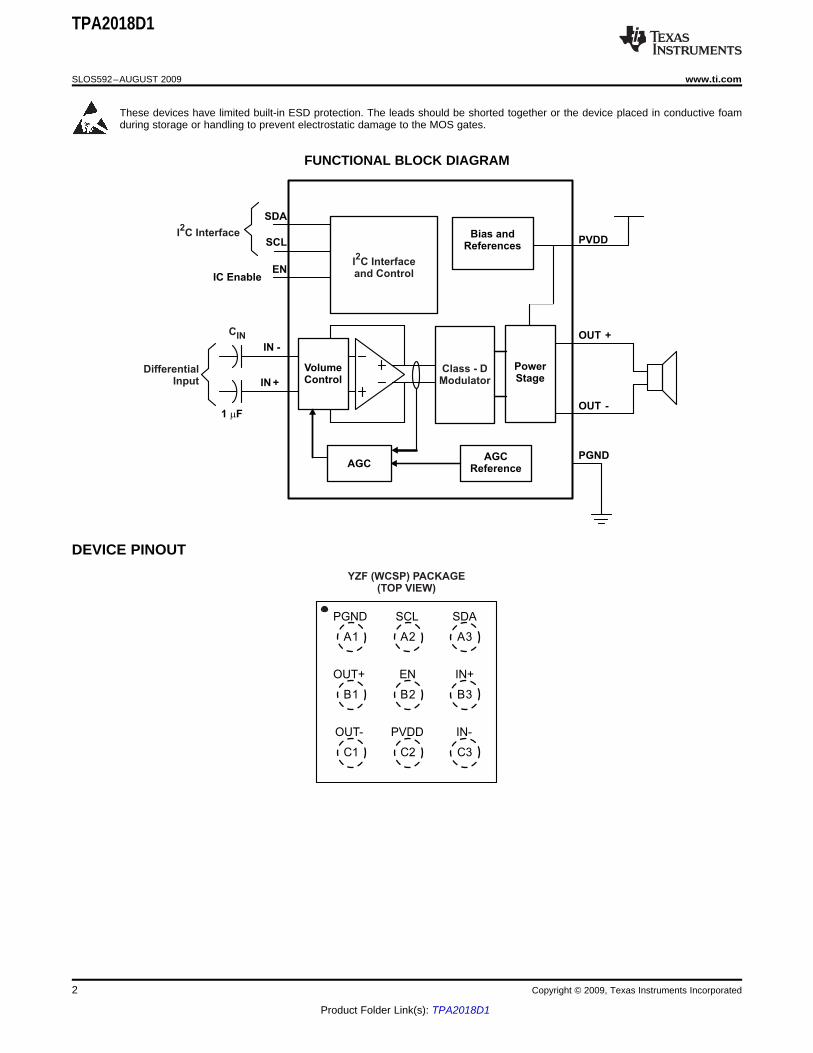
VolumeControl
1 Fm
IC Enable
PowerStage
AGCReference
Bias andReferences
AGC
I C Interface2
DifferentialInput
CIN
I C Interfaceand Control
2
Class - DModulator
DEVICE PINOUT
IN-
PGND
ENOUT+
PVDDOUT-
SCL
IN+
SDA
C1 C2 C3
B1 B3B2
A1 A2 A3
YZF (WCSP) PACKAGE(TOP VIEW)
TPA2018D1
SLOS592–AUGUST 2009 ................................................................................................................................................................................................ www.ti.com
These devices have limited built-in ESD protection. The leads should be shorted together or the device placed in conductive foamduring storage or handling to prevent electrostatic damage to the MOS gates.
FUNCTIONAL BLOCK DIAGRAM
2 Copyright © 2009, Texas Instruments Incorporated
Product Folder Link(s): TPA2018D1

ABSOLUTE MAXIMUM RATINGS (1)
DISSIPATION RATINGS TABLE (1)
TPA2018D1
www.ti.com ................................................................................................................................................................................................ SLOS592–AUGUST 2009
TERMINAL FUNCTIONSTERMINAL I/O/P DESCRIPTION
NAME WCSPEN B2 I Enable terminal (active high)IN+ B3 I Positive audio inputIN– C3 I Negative audio inputOUT+ B1 O Positive differential outputOUT– C1 O Negative differential outputPGND A1 P Power groundPVDD C2 P Power supplySCL A2 I I2C clock interfaceSDA A3 I/O I2C data interface
over operating free-air temperature range (unless otherwise noted).
VALUE / UNITVDD Supply voltage PVDD –0.3 V to 6.0 V
EN, IN+, IN– –0.3 V to VDD+0.3 VInput voltage
SDA, SCL –0.3 V to 6.0 VSee Dissipation RatingsContinuous total power dissipation Table
TA Operating free-air temperature range –40°C to +85°CTJ Operating junction temperature range –40°C to +150°CTstg Storage temperature range –65°C to +150°CESD Electro-Static Discharge Tolerance, all pins Human Body Model (HBM) 2 kV
Charged Device Model (CDM) 500 VRLOAD Minimum load resistance 3.2 Ω
(1) Stresses beyond those listed under "absolute maximum ratings" may cause permanent damage to the device. These are stress ratingsonly, and functional operation of the device at these or any other conditions beyond those indicated under "recommended operatingconditions" is not implied. Exposure to absolute-maximum-rated conditions for extended periods may affect device reliability.
PACKAGE TA ≤ +25°C DERATING FACTOR TA = +70°C TA = +85°C9-ball WCSP 1.19 W 9.52 mW/°C 0.76 W 0.62 W
(1) Dissipation ratings are for a 2-side, 2-plane PCB.
Copyright © 2009, Texas Instruments Incorporated 3
Product Folder Link(s): TPA2018D1
RECOMMENDED OPERATING CONDITIONS
ELECTRICAL CHARACTERISTICS
TPA2018D1
SLOS592–AUGUST 2009 ................................................................................................................................................................................................ www.ti.com
AVAILABLE OPTIONS (1)
TA PACKAGED DEVICES (2) PART NUMBER SYMBOLTPA2018D1YZFR OBC
–40°C to 85°C 9-ball, WCSPTPA2018D1YZFT OBC
(1) For the most current package and ordering information, see the Package Option Addendum at the end of this document, or see the TIWeb site at www.ti.com
(2) The YZF packages are only available taped and reeled. The suffix R indicates a reel of 3000; the suffix T indicates a reel of 250.
MIN MAX UNITVDD Supply voltage PVDD 2.5 5.5 VVIH High-level input voltage EN, SDA, SCL 1.3 VVIL Low-level input voltage EN, SDA, SCL 0.6 VTA Operating free-air temperature –40 +85 °C
at TA = 25°C, VDD = 3.6 V, SDZ = 1.3 V, and RL = 8 Ω + 33 µH (unless otherwise noted).
PARAMETER TEST CONDITIONS MIN TYP MAX UNITVDD Supply voltage range 2.5 3.6 5.5 V
EN = 0.35 V, VDD = 2.5 V 0.1 1ISDZ Shutdown quiescent current EN = 0.35 V, VDD = 3.6 V 0.2 1 µA
EN = 0.35 V, VDD = 5.5 V 0.3 1EN = 1.3 V, VDD = 2.5 V 35 50
Software shutdown quiescentISWS EN = 1.3 V, VDD = 3.6 V 50 70 µAcurrentEN = 1.3 V, VDD = 5.5 V 75 100VDD = 2.5 V 1.5 2.5
IDD Supply current VDD = 3.6 V 1.7 2.7 mAVDD = 5.5 V 2 3.5
fSW Class D Switching Frequency 275 300 325 kHzIIH High-level input current VDD = 5.5 V, EN = 5.8 V 1 µAIIL Low-level input current VDD = 5.5 V, EN = –0.3 V –1 µAtSTART Start-up time 2.5 V ≤ VDD ≤ 5.5 V no pop, CIN ≤ 1 µF 5 msPOR Power on reset ON threshold 2 2.3 VPOR Power on reset hysteresis 0.2 V
RL = 8 Ω, Vicm = 0.5 V and Vicm = VDD – 0.8 V,CMRR Input common mode rejection –75 dBdifferential inputs shortedVDD = 3.6 V, AV = 6 dB, RL = 8 Ω, inputs acVoo Output offset voltage 1.5 10 mVgrounded
Output Impedance in shutdown 2 kΩZOUT EN = 0.35 VmodeGain accuracy Compression and limiter disabled, Gain = 0 to 30 dB –0.5 0.5 dB
PSRR Power supply rejection ratio VDD = 2.5 V to 4.7 V -80 dB
4 Copyright © 2009, Texas Instruments Incorporated
Product Folder Link(s): TPA2018D1
OPERATING CHARACTERISTICS
TPA2018D1
IN+
IN–
OUT+
OUT–
VDD
VDD
GND
CI
CI
MeasurementOutput
+
+
–
–
Load30 kHz
Low-PassFilter
MeasurementInput
+
–
1 Fm
TPA2018D1
www.ti.com ................................................................................................................................................................................................ SLOS592–AUGUST 2009
at TA = 25°C, VDD = 3.6V, EN = 1.3 V, RL = 8 Ω +33 µH, and AV = 6 dB (unless otherwise noted).
PARAMETER TEST CONDITIONS MIN TYP MAX UNITkSVR power-supply ripple rejection ratio VDD = 3.6 Vdc with ac of 200 mVPP at 217 Hz –70 dB
faud_in = 1 kHz; PO = 550 mW; VDD = 3.6 V 0.1%faud_in = 1 kHz; PO = 1.25 W; VDD = 5 V 0.1%
THD+N Total harmonic distortion + noisefaud_in = 1 kHz; PO = 710 mW; VDD = 3.6 V 1%faud_in = 1 kHz; PO = 1.4 W; VDD = 5 V 1%
NfonF Output integrated noise Av = 6 dB 42 µVNfoA Output integrated noise Av = 6 dB floor, A-weighted 30 µVFR Frequency response Av = 6 dB 20 20000 Hz
THD+N = 10%, VDD = 5 V, RL = 8 Ω 1.72 WTHD+N = 10%, VDD = 3.6 V, RL = 8 Ω 880 mWTHD+N = 1%, VDD = 5 V, RL = 8 Ω 1.4 W
Pomax Maximum output powerTHD+N = 1% , VDD = 3.6 V, RL = 8 Ω 710 mWTHD+N = 1% , VDD = 5 V, RL = 4 Ω 2.5 WTHD+N = 10% , VDD = 5 V, RL = 4 Ω 3 WTHD+N = 1%, VDD = 3.6 V, RL = 8 Ω, PO= 0.71 W 91%
η EfficiencyTHD+N = 1%, VDD = 5 V, RL = 8 Ω, PO = 1.4 W 93%
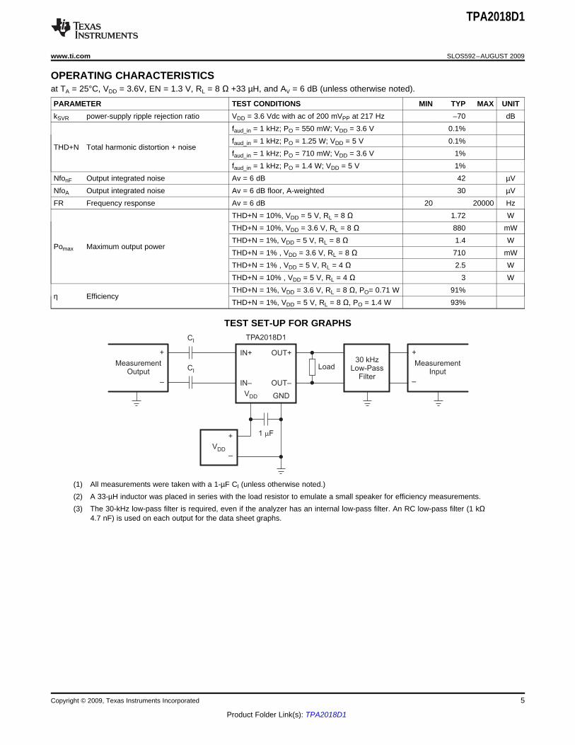
TEST SET-UP FOR GRAPHS
(1) All measurements were taken with a 1-µF CI (unless otherwise noted.)(2) A 33-µH inductor was placed in series with the load resistor to emulate a small speaker for efficiency measurements.(3) The 30-kHz low-pass filter is required, even if the analyzer has an internal low-pass filter. An RC low-pass filter (1 kΩ
4.7 nF) is used on each output for the data sheet graphs.
Copyright © 2009, Texas Instruments Incorporated 5
Product Folder Link(s): TPA2018D1

I2C TIMING CHARACTERISTICS
SCL
SDA
tw(H) tw(L)
tsu1th1
SCL
SDA
th2t(buf)
tsu2 tsu3
Start Condition Stop Condition
TPA2018D1
SLOS592–AUGUST 2009 ................................................................................................................................................................................................ www.ti.com
For I2C Interface Signals Over Recommended Operating Conditions (unless otherwise noted)
PARAMETER TEST CONDITIONS MIN TYP MAX UNITfSCL Frequency, SCL No wait states 400 kHztW(H) Pulse duration, SCL high 0.6 µstW(L) Pulse duration, SCL low 1.3 µstSU(1) Setup time, SDA to SCL 100 nsth1 Hold time, SCL to SDA 10 nst(buf) Bus free time between stop and start 1.3 µs
conditiontSU2 Setup time, SCL to start condition 0.6 µsth2 Hold time, start condition to SCL 0.6 µstSU3 Setup time, SCL to stop condition 0.6 µs
Figure 1. SCL and SDA Timing
Figure 2. Start and Stop Conditions Timing
6 Copyright © 2009, Texas Instruments Incorporated
Product Folder Link(s): TPA2018D1

TYPICAL CHARACTERISTICS
Table of Graphs
VDD − Supply Voltage − V
0
1
2
3
4
5
6
7
8
9
10
2.5 3.0 3.5 4.0 4.5 5.0 5.5
I DD
− Q
uies
cent
Sup
ply
Cur
rent
− m
A
G001
RL = 8 Ω + 33 µHEN = VDD
VDD − Supply Voltage − V
0
10
20
30
40
50
60
70
80
90
100
2.5 3.0 3.5 4.0 4.5 5.0 5.5
I DD
− S
uppl
y C
urre
nt −
µA
G002
En = 0 V
SWS = 1
RL = 8 Ω + 33 µH
TPA2018D1
www.ti.com ................................................................................................................................................................................................ SLOS592–AUGUST 2009
with C(DECOUPLE) = 1 µF, CI = 1 µF.All THD + N graphs are taken with outputs out of phase (unless otherwise noted).
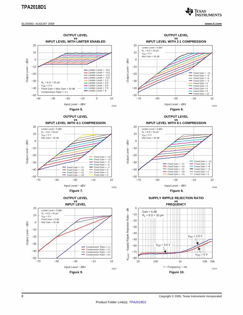
FIGUREQuiescent supply current vs Supply voltage Figure 3Supply current vs Supply voltage in shutdown Figure 4
vs Input level with limiter enabled Figure 5vs Input level with 2:1 compression Figure 6
Output level vs Input level with 4:1 compression Figure 7vs Input level with 8:1 compression Figure 8vs Input level Figure 9
Supply ripple rejection ratio vs Frequency Figure 10vs Frequency [RL = 8 Ω, VDD = 3.6 V] Figure 11vs Frequency [RL = 8 Ω, VDD = 5 V] Figure 12
Total harmonic distortion + noisevs Frequency [RL = 4 Ω, VDD = 3.6 V] Figure 13vs Frequency [RL = 4 Ω, VDD = 5 V] Figure 14vs Output power [RL = 8 Ω] Figure 15
Total harmonic distortion + noisevs Output power [RL = 4 Ω] Figure 16vs Output power [per channel, RL = 8 Ω] Figure 17
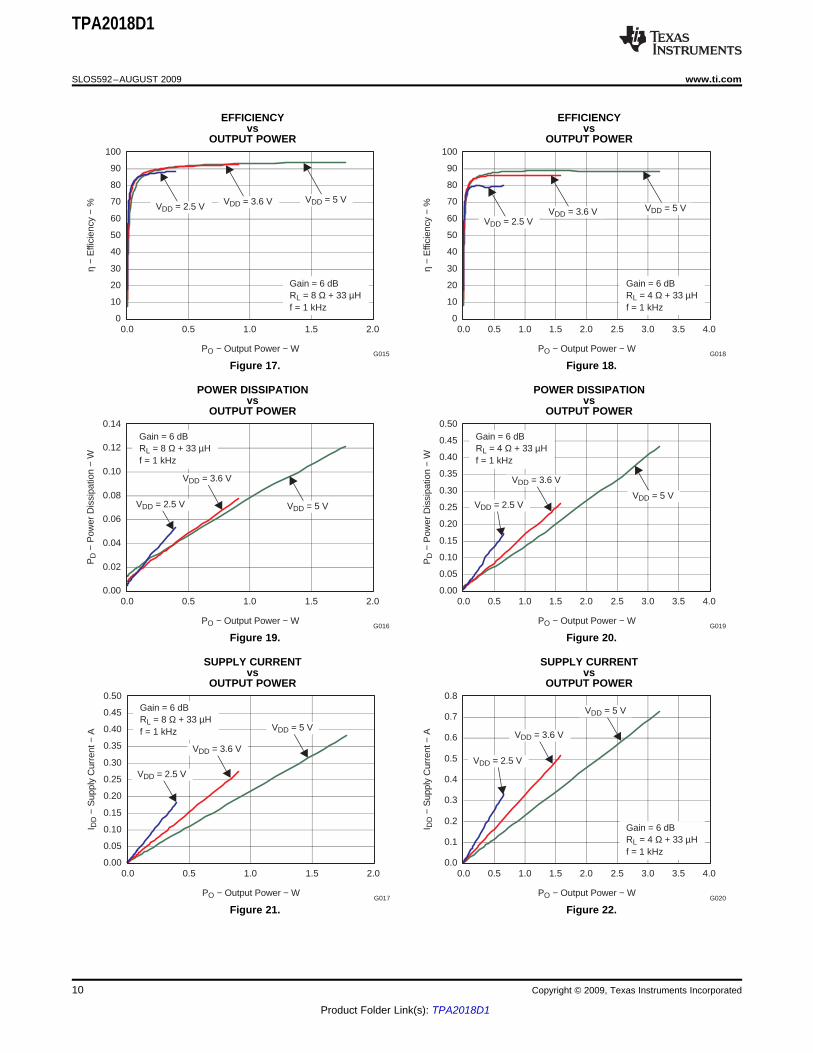
Efficiencyvs Output power [per channel, RL = 4 Ω] Figure 18vs Output power [RL = 8 Ω] Figure 19
Power dissipationvs Output power [RL = 4 Ω] Figure 20vs Output power [RL = 8 Ω] Figure 21
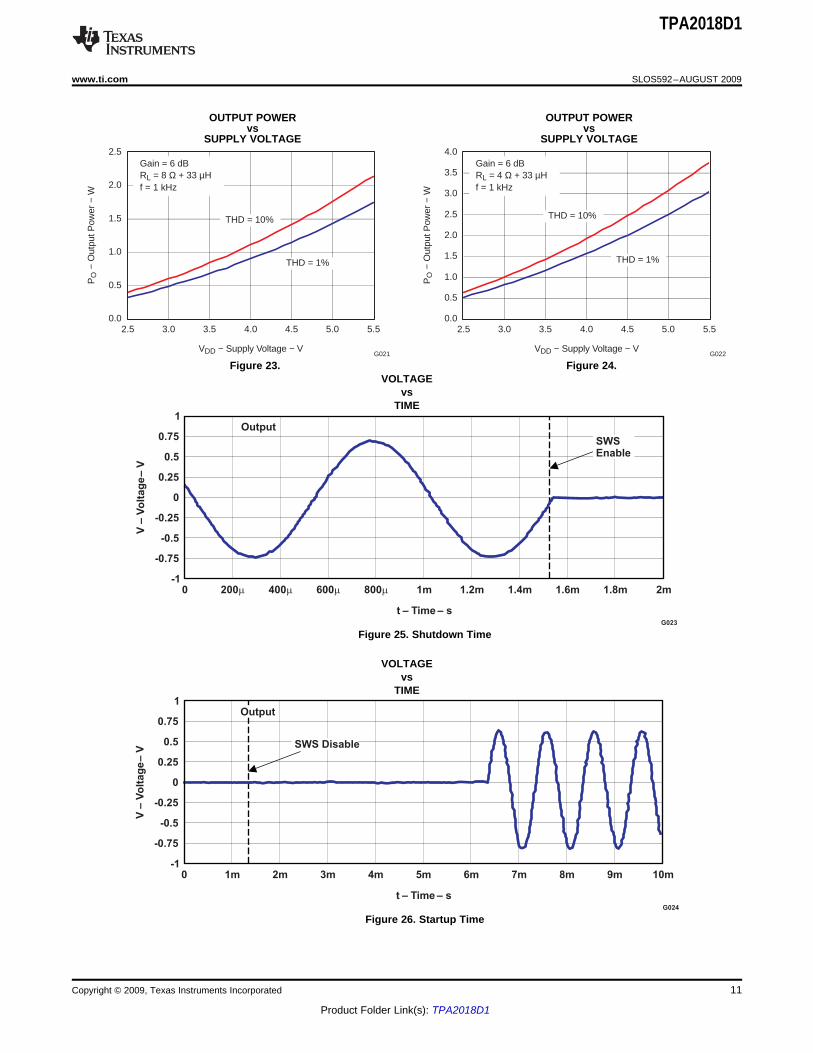
Supply currentvs Output power [RL = 4 Ω] Figure 22vs Supply voltage [RL = 8 Ω] Figure 23
Output powervs Supply voltage [RL = 4 Ω] Figure 24
Shutdown time Figure 25Startup time Figure 26
QUIESCENT SUPPLY CURRENT SUPPLY CURRENTvs vs
SUPPLY VOLTAGE SUPPLY VOLTAGE IN SHUTDOWN
Figure 3. Figure 4.
Copyright © 2009, Texas Instruments Incorporated 7
Product Folder Link(s): TPA2018D1
Input Level − dBV
−50
−40
−30
−20
−10
0
10
20
−40 −30 −20 −10 0 10
Out
put L
evel
− d
BV
G003
RL = 8 Ω + 33 µHVDD = 5 VFixed Gain = Max Gain = 30 dBCompression Ratio = 1:1
Limiter Level = −6.5Limiter Level = −4.5Limiter Level = −2.5Limiter Level = −0.5Limiter Level = 1.5Limiter Level = 3.5Limiter Level = 5.5Limiter Level = 7.5Limiter Level = 9
Input Level − dBV
−50
−40
−30
−20
−10
0
10
20
−70 −50 −30 −10 10
Out
put L
evel
− d
BV
G004
Limiter Level = 9 dBVRL = 8 Ω + 33 µHVDD = 5 VMax Gain = 30 dB
Fixed Gain = −12Fixed Gain = −9Fixed Gain = −6Fixed Gain = −3Fixed Gain = 0Fixed Gain = 3Fixed Gain = 6Fixed Gain = 9Fixed Gain = 12
Input Level − dBV
−50
−40
−30
−20
−10
0
10
20
−70 −50 −30 −10 10
Out
put L
evel
− d
BV
G005
Limiter Level = 9 dBVRL = 8 Ω + 33 µHVDD = 5 VMax Gain = 30 dB
Fixed Gain = −15Fixed Gain = −12Fixed Gain = −9Fixed Gain = −6Fixed Gain = −3Fixed Gain = 0Fixed Gain = 3Fixed Gain = 6
Fixed Gain = −27Fixed Gain = −24Fixed Gain = −21Fixed Gain = −18
Input Level − dBV
−50
−40
−30
−20
−10
0
10
20
−70 −50 −30 −10 10
Out
put L
evel
− d
BV
G006
Limiter Level = 9 dBVRL = 8 Ω + 33 µHVDD = 5 VMax Gain = 30 dB
Fixed Gain = −12Fixed Gain = −9Fixed Gain = −6Fixed Gain = −3Fixed Gain = 0Fixed Gain = 3
Fixed Gain = −27Fixed Gain = −24Fixed Gain = −21Fixed Gain = −18Fixed Gain = −15
Input Level − dBV
−50
−40
−30
−20
−10
0
10
20
−70 −50 −30 −10 10
Out
put L
evel
− d
BV
G007
Compression Ratio = 1:1Compression Ratio = 2:1Compression Ratio = 4:1Compression Ratio = 8:1
Limiter Level = 9 dBVRL = 8 Ω + 33 µHVDD = 5 VFixed Gain = 0 dBMax Gain = 30 dB
−80
−70
−60
−50
−40
−30
−20
−10
0
f − Frequency − Hz
KS
VR
− S
uppl
y R
ippl
e R
ejec
tion
Rat
io −
dB
G014
Gain = 6 dBRL = 8 Ω + 33 µH
20 100 1k 20k10k
VDD = 2.5 V
VDD = 5 V
VDD = 3.6 V
TPA2018D1
SLOS592–AUGUST 2009 ................................................................................................................................................................................................ www.ti.com
OUTPUT LEVEL OUTPUT LEVELvs vs
INPUT LEVEL WITH LIMITER ENABLED INPUT LEVEL WITH 2:1 COMPRESSION
Figure 5. Figure 6.
OUTPUT LEVEL OUTPUT LEVELvs vs
INPUT LEVEL WITH 4:1 COMPRESSION INPUT LEVEL WITH 8:1 COMPRESSION
Figure 7. Figure 8.
OUTPUT LEVEL SUPPLY RIPPLE REJECTION RATIOvs vs
INPUT LEVEL FREQUENCY
Figure 9. Figure 10.
8 Copyright © 2009, Texas Instruments Incorporated
Product Folder Link(s): TPA2018D1

f − Frequency − Hz
TH
D+N
− T
otal
Har
mon
ic D
isto
rtio
n +
Noi
se −
%
20 100 1k 20k
10
0.1
0.01
0.001
G008
Gain = 6 dBRL = 8 Ω + 33 µHVDD = 3.6 V1
10k
PO = 0.05 W
PO = 0.5 W
PO = 0.25 W
f − Frequency − Hz
TH
D+N
− T
otal
Har
mon
ic D
isto
rtio
n +
Noi
se −
%
20 100 1k 20k
10
0.1
0.01
0.001
G009
Gain = 6 dBRL = 8 Ω + 33 µHVDD = 5 V1
10k
PO = 0.5 W
PO = 0.1 W
PO = 1 W
f − Frequency − Hz
TH
D+N
− T
otal
Har
mon
ic D
isto
rtio
n +
Noi
se −
%
20 100 1k 20k
10
0.1
0.01
0.001
G010
Gain = 6 dBRL = 4 Ω + 33 µHVDD = 3.6 V1
10k
PO = 0.1 W
PO = 1 W
PO = 0.5 W
f − Frequency − Hz
TH
D+N
− T
otal
Har
mon
ic D
isto
rtio
n +
Noi
se −
%
20 100 1k 20k
10
0.1
0.01
0.001
G011
Gain = 6 dBRL = 4 Ω + 33 µHVDD = 5 V1
10k
PO = 0.2 W
PO = 1 W
PO = 2 W
PO − Output Power − W
TH
D+N
− T
otal
Har
mon
ic D
isto
rtio
n +
Noi
se −
%
0.01 0.1 1 3
100
1
0.1
0.01
G012
Gain = 6 dBRL = 8 Ω + 33 µHf = 1 kHz10
VDD = 3.6 V
VDD = 5 V
PO − Output Power − W
TH
D+N
− T
otal
Har
mon
ic D
isto
rtio
n +
Noi
se −
%
0.01 0.1 1 5
100
1
0.1
0.01
G013
Gain = 6 dBRL = 4 Ω + 33 µHf = 1 kHz10
VDD = 3.6 V
VDD = 5 V
TPA2018D1
www.ti.com ................................................................................................................................................................................................ SLOS592–AUGUST 2009
TOTAL HARMONIC DISTORTION + NOISE TOTAL HARMONIC DISTORTION + NOISEvs vs
FREQUENCY FREQUENCY
Figure 11. Figure 12.
TOTAL HARMONIC DISTORTION + NOISE TOTAL HARMONIC DISTORTION + NOISEvs vs
FREQUENCY FREQUENCY
Figure 13. Figure 14.
TOTAL HARMONIC DISTORTION + NOISE TOTAL HARMONIC DISTORTION + NOISEvs vs
OUTPUT POWER OUTPUT POWER
Figure 15. Figure 16.
Copyright © 2009, Texas Instruments Incorporated 9
Product Folder Link(s): TPA2018D1
PO − Output Power − W
0
10
20
30
40
50
60
70
80
90
100
0.0 0.5 1.0 1.5 2.0
η −
Effi
cien
cy −
%
G015
Gain = 6 dBRL = 8 Ω + 33 µHf = 1 kHz
VDD = 2.5 V VDD = 3.6 V VDD = 5 V
PO − Output Power − W
0
10
20
30
40
50
60
70
80
90
100
0.0 0.5 1.0 1.5 2.0 2.5 3.0 3.5 4.0
η −
Effi
cien
cy −
%
G018
Gain = 6 dBRL = 4 Ω + 33 µHf = 1 kHz
VDD = 2.5 VVDD = 3.6 V VDD = 5 V
PO − Output Power − W
0.00
0.02
0.04
0.06
0.08
0.10
0.12
0.14
0.0 0.5 1.0 1.5 2.0
PD
− P
ower
Dis
sipa
tion
− W
G016
Gain = 6 dBRL = 8 Ω + 33 µHf = 1 kHz
VDD = 5 V
VDD = 3.6 V
VDD = 2.5 V
PO − Output Power − W
0.00
0.05
0.10
0.15
0.20
0.25
0.30
0.35
0.40
0.45
0.50
0.0 0.5 1.0 1.5 2.0 2.5 3.0 3.5 4.0
PD
− P
ower
Dis
sipa
tion
− W
G019
Gain = 6 dBRL = 4 Ω + 33 µHf = 1 kHz
VDD = 5 V
VDD = 3.6 V
VDD = 2.5 V
PO − Output Power − W
0.00
0.05
0.10
0.15
0.20
0.25
0.30
0.35
0.40
0.45
0.50
0.0 0.5 1.0 1.5 2.0
I DD
− S
uppl
y C
urre
nt −
A
G017
Gain = 6 dBRL = 8 Ω + 33 µHf = 1 kHz
VDD = 3.6 V
VDD = 2.5 V
VDD = 5 V
PO − Output Power − W
0.0
0.1
0.2
0.3
0.4
0.5
0.6
0.7
0.8
0.0 0.5 1.0 1.5 2.0 2.5 3.0 3.5 4.0
I DD
− S
uppl
y C
urre
nt −
A
G020
VDD = 3.6 V
VDD = 2.5 V
VDD = 5 V
Gain = 6 dBRL = 4 Ω + 33 µHf = 1 kHz
TPA2018D1
SLOS592–AUGUST 2009 ................................................................................................................................................................................................ www.ti.com
EFFICIENCY EFFICIENCYvs vs
OUTPUT POWER OUTPUT POWER
Figure 17. Figure 18.
POWER DISSIPATION POWER DISSIPATIONvs vs
OUTPUT POWER OUTPUT POWER
Figure 19. Figure 20.
SUPPLY CURRENT SUPPLY CURRENTvs vs
OUTPUT POWER OUTPUT POWER
Figure 21. Figure 22.
10 Copyright © 2009, Texas Instruments Incorporated
Product Folder Link(s): TPA2018D1
VDD − Supply Voltage − V
0.0
0.5
1.0
1.5
2.0
2.5
2.5 3.0 3.5 4.0 4.5 5.0 5.5
PO
− O
utpu
t Pow
er −
W
G021
Gain = 6 dBRL = 8 Ω + 33 µHf = 1 kHz
THD = 1%
THD = 10%
VDD − Supply Voltage − V
0.0
0.5
1.0
1.5
2.0
2.5
3.0
3.5
4.0
2.5 3.0 3.5 4.0 4.5 5.0 5.5
PO
− O
utpu
t Pow
er −
W
G022
Gain = 6 dBRL = 4 Ω + 33 µHf = 1 kHz
THD = 1%
THD = 10%
1
0.5
0.75
0.25
0
-0.25
-0.5
-0.75
-10 400m200m 600m 800m 1m 1.2m 1.6m1.4m 1.8m 2m
t – Time – s
V–
Vo
ltag
e–
V
SWSEnable
Output
G023
1
0.5
0.75
0.25
0
-0.25
-0.5
-0.75
-10 2m1m 3m 4m 5m 6m 8m7m 9m 10m
t – Time – s
V–
Vo
ltag
e–
V SWS Disable
Output
G024
TPA2018D1
www.ti.com ................................................................................................................................................................................................ SLOS592–AUGUST 2009
OUTPUT POWER OUTPUT POWERvs vs
SUPPLY VOLTAGE SUPPLY VOLTAGE
Figure 23. Figure 24.VOLTAGE
vsTIME
Figure 25. Shutdown Time
VOLTAGEvs
TIME
Figure 26. Startup Time
Copyright © 2009, Texas Instruments Incorporated 11
Product Folder Link(s): TPA2018D1
APPLICATION INFORMATION
AUTOMATIC GAIN CONTROL
TPA2018D1
SLOS592–AUGUST 2009 ................................................................................................................................................................................................ www.ti.com
The Automatic Gain Control (AGC) feature provides continuous automatic gain adjustment to the amplifierthrough an internal PGA. This feature enhances the perceived audio loudness and at the same time preventsspeaker damage from occurring (Limiter function).
The AGC function attempts to maintain the audio signal gain as selected by the user through the Fixed Gain,Limiter Level, and Compression Ratio variables. Other advanced features included are Maximum Gain and NoiseGate Threshold. Table 1 describes the function of each variable in the AGC function.
Table 1. TPA2018D1 AGC Variable DescriptionsVARIABLE DESCRIPTION
Maximum Gain The gain at the lower end of the compression region.Fixed Gain The normal gain of the device when the AGC is inactive.
The fixed gain is also the initial gain when the device comes out of shutdown mode or when the AGC isdisabled.
Limiter Level The value that sets the maximum allowed output amplitude.Compression Ratio The relation between input and output voltage.Noise Gate Threshold Below this value, the AGC holds the gain to prevent breathing effects.Attack Time The minimum time between two gain decrements.Release Time The minimum time between two gain increments.Hold Time The time it takes for the very first gain increment after the input signal amplitude decreases.
12 Copyright © 2009, Texas Instruments Incorporated
Product Folder Link(s): TPA2018D1

Release Time
E
Limiter threshold
GAIN
AC
B
D
Attack Time
Limiter threshold
Limiter threshold
Hold Time
INP
UT
SIG
NA
LO
UT
PU
T S
IGN
AL
Limiter threshold
TPA2018D1
www.ti.com ................................................................................................................................................................................................ SLOS592–AUGUST 2009
The AGC works by detecting the audio input envelope. The gain changes depending on the amplitude, the limiterlevel, the compression ratio, and the attack and release time. The gain changes constantly as the audio signalincreases and/or decreases to create the compression effect. The gain step size for the AGC is 0.5 dB. If theaudio signal has near-constant amplitude, the gain does not change. Figure 27 shows how the AGC works.
A. Gain decreases with no delay; attack time is reset. Release time and hold time are reset.B. Signal amplitude above limiter level, but gain cannot change because attack time is not over.C. Attack time ends; gain is allowed to decrease from this point forward by one step. Gain decreases because the
amplitude remains above limiter threshold. All times are resetD. Gain increases after release time finishes and signal amplitude remains below desired level. All times are reset after
the gain increase.E. Gain increases after release time is finished again because signal amplitude remains below desired level. All times
are reset after the gain increase.
Figure 27. Input and Output Audio Signal vs Time
Since the number of gain steps is limited the compression region is limited as well. The following figure showshow the gain changes vs. the input signal amplitude in the compression region.
Copyright © 2009, Texas Instruments Incorporated 13
Product Folder Link(s): TPA2018D1
Gain
- d
B
V - dBVIN
V-
dB
VO
UT
V - dBVIN
IncreasingFixed Gain
DecreasingFixed Gain
Fixed
Gai
n = 6
dB
Fixed
Gai
n = 3
dB
1:1
TPA2018D1
SLOS592–AUGUST 2009 ................................................................................................................................................................................................ www.ti.com
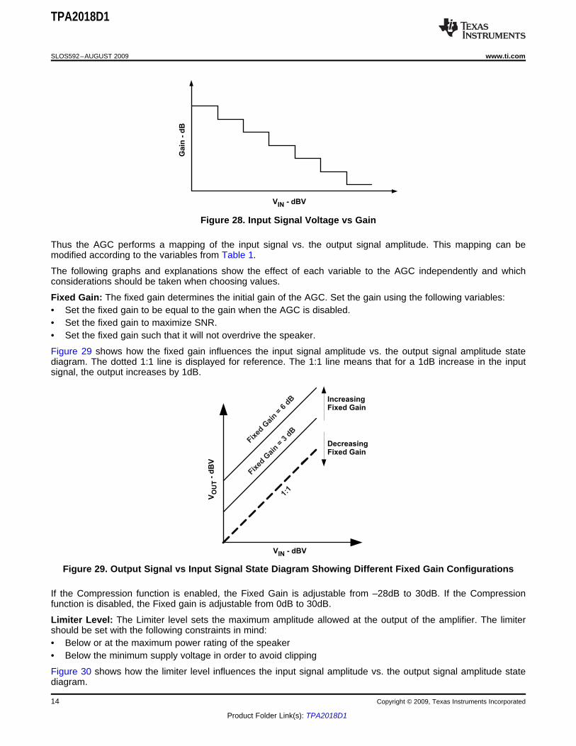
Figure 28. Input Signal Voltage vs Gain
Thus the AGC performs a mapping of the input signal vs. the output signal amplitude. This mapping can bemodified according to the variables from Table 1.
The following graphs and explanations show the effect of each variable to the AGC independently and whichconsiderations should be taken when choosing values.
Fixed Gain: The fixed gain determines the initial gain of the AGC. Set the gain using the following variables:• Set the fixed gain to be equal to the gain when the AGC is disabled.• Set the fixed gain to maximize SNR.• Set the fixed gain such that it will not overdrive the speaker.
Figure 29 shows how the fixed gain influences the input signal amplitude vs. the output signal amplitude statediagram. The dotted 1:1 line is displayed for reference. The 1:1 line means that for a 1dB increase in the inputsignal, the output increases by 1dB.
Figure 29. Output Signal vs Input Signal State Diagram Showing Different Fixed Gain Configurations
If the Compression function is enabled, the Fixed Gain is adjustable from –28dB to 30dB. If the Compressionfunction is disabled, the Fixed gain is adjustable from 0dB to 30dB.
Limiter Level: The Limiter level sets the maximum amplitude allowed at the output of the amplifier. The limitershould be set with the following constraints in mind:• Below or at the maximum power rating of the speaker• Below the minimum supply voltage in order to avoid clipping
Figure 30 shows how the limiter level influences the input signal amplitude vs. the output signal amplitude statediagram.
14 Copyright © 2009, Texas Instruments Incorporated
Product Folder Link(s): TPA2018D1
V-
dB
VO
UT
V - dBVIN
IncreasingLimiterLevel
DecreasingLimiterLevel
Limiter Level= 500mW
Limiter Level= 630mW
= 400Limiter Level mW
V-
dB
VO
UT
V - dBVIN
1:1
Large Fixed Gain
SmallFixed
Gain
Input signal initial amplitude - |Current input signal amplitude|Output signal amplitude =
Compression ratio (1)
0dBV | 32 dBV|8dBV =
4
- -
-
(2)
TPA2018D1
www.ti.com ................................................................................................................................................................................................ SLOS592–AUGUST 2009
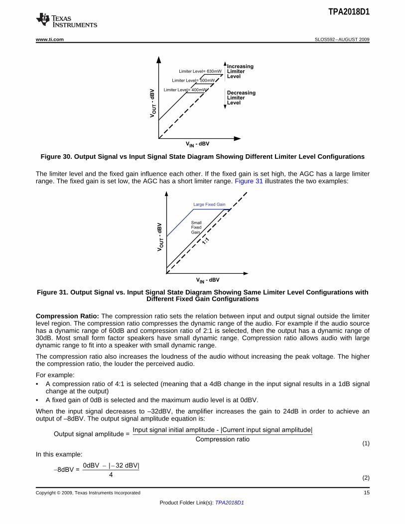
Figure 30. Output Signal vs Input Signal State Diagram Showing Different Limiter Level Configurations
The limiter level and the fixed gain influence each other. If the fixed gain is set high, the AGC has a large limiterrange. The fixed gain is set low, the AGC has a short limiter range. Figure 31 illustrates the two examples:
Figure 31. Output Signal vs. Input Signal State Diagram Showing Same Limiter Level Configurations withDifferent Fixed Gain Configurations
Compression Ratio: The compression ratio sets the relation between input and output signal outside the limiterlevel region. The compression ratio compresses the dynamic range of the audio. For example if the audio sourcehas a dynamic range of 60dB and compression ratio of 2:1 is selected, then the output has a dynamic range of30dB. Most small form factor speakers have small dynamic range. Compression ratio allows audio with largedynamic range to fit into a speaker with small dynamic range.
The compression ratio also increases the loudness of the audio without increasing the peak voltage. The higherthe compression ratio, the louder the perceived audio.
For example:• A compression ratio of 4:1 is selected (meaning that a 4dB change in the input signal results in a 1dB signal
change at the output)• A fixed gain of 0dB is selected and the maximum audio level is at 0dBV.
When the input signal decreases to –32dBV, the amplifier increases the gain to 24dB in order to achieve anoutput of –8dBV. The output signal amplitude equation is:
In this example:
Copyright © 2009, Texas Instruments Incorporated 15
Product Folder Link(s): TPA2018D1

1Gain change = 1 × Input signal change
Compression ratio
æ ö-ç ÷
è ø (3)
124 dB = 1 × 32
4
æ ö-ç ÷
è ø (4)
V-
dB
VO
UT
V - dBVIN
IncreasingFixed Gain
Decreasing
1:1
2 :1
4 :1
8 :1
1:1
2 :1
4 :1
8 :1
RotationPoint@lower gain
RotationPoint@higher gain
TPA2018D1
SLOS592–AUGUST 2009 ................................................................................................................................................................................................ www.ti.com
The gain change equation is:
Consider the following when setting the compression ratio:• Dynamic range of the speaker• Fixed gain level• Limiter Level• Audio Loudness vs Output Dynamic Range.
Figure 32 shows different settings for dynamic range and different fixed gain selected but no limiter level.
Figure 32. Output Signal vs Input Signal State Diagram Showing Different Compression RatioConfigurations with Different Fixed Gain Configurations
The rotation point is always at Vin = 10dBV. The rotation point is not located at the intersection of the limiterregion and the compression region. By changing the fixed gain the rotation point will move in the y-axis directiononly, as shown in the previous graph.
Interaction between compression ratio and limiter range: The compression ratio can be limited by the limiterrange. Note that the limiter range is selected by the limiter level and the fixed gain.
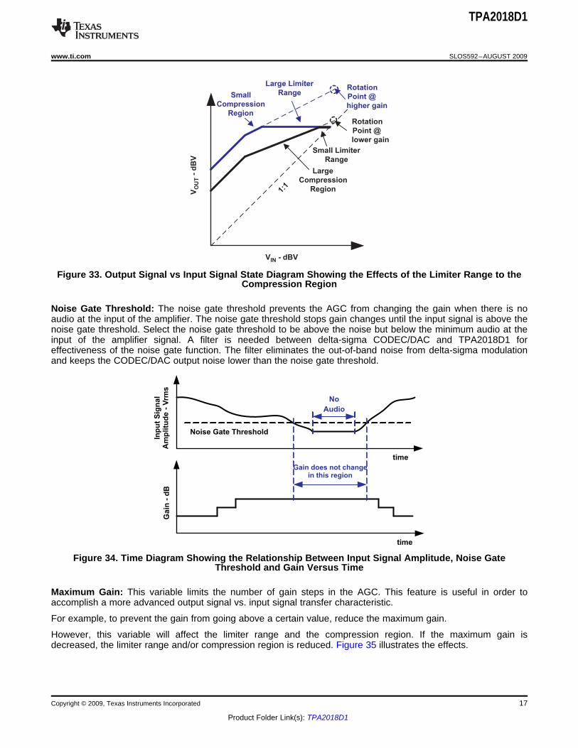
For a setting with large limiter range, the amount of gain steps in the AGC remaining to perform compression arelimited. Figure 33 shows two examples, where the fixed gain was changed.1. Small limiter range yielding a large compression region (small fixed gain).2. Large limiter range yielding a small compression region (large fixed gain).
16 Copyright © 2009, Texas Instruments Incorporated
Product Folder Link(s): TPA2018D1
VO
UT
- d
BV
V - dBVIN
1:1
Large Limiter
RangeSmall
Compression
Region
Large
Compression
Region
Small Limiter
Range
Rotation
Point @
lower gain
Rotation
Point @
higher gain
time
Gain
- d
B
Inp
ut
Sig
nal
Am
plitu
de -
Vrm
s
time
Noise Gate Threshold
No
Audio
Gain does not changein this region
TPA2018D1
www.ti.com ................................................................................................................................................................................................ SLOS592–AUGUST 2009
Figure 33. Output Signal vs Input Signal State Diagram Showing the Effects of the Limiter Range to theCompression Region
Noise Gate Threshold: The noise gate threshold prevents the AGC from changing the gain when there is noaudio at the input of the amplifier. The noise gate threshold stops gain changes until the input signal is above thenoise gate threshold. Select the noise gate threshold to be above the noise but below the minimum audio at theinput of the amplifier signal. A filter is needed between delta-sigma CODEC/DAC and TPA2018D1 foreffectiveness of the noise gate function. The filter eliminates the out-of-band noise from delta-sigma modulationand keeps the CODEC/DAC output noise lower than the noise gate threshold.
Figure 34. Time Diagram Showing the Relationship Between Input Signal Amplitude, Noise GateThreshold and Gain Versus Time
Maximum Gain: This variable limits the number of gain steps in the AGC. This feature is useful in order toaccomplish a more advanced output signal vs. input signal transfer characteristic.
For example, to prevent the gain from going above a certain value, reduce the maximum gain.
However, this variable will affect the limiter range and the compression region. If the maximum gain isdecreased, the limiter range and/or compression region is reduced. Figure 35 illustrates the effects.
Copyright © 2009, Texas Instruments Incorporated 17
Product Folder Link(s): TPA2018D1

V-
dB
VO
UT
V - dBVIN
Max Gain
= 22dB
Max Gain
= 30dB
1:1
TPA2018D1
SLOS592–AUGUST 2009 ................................................................................................................................................................................................ www.ti.com
Figure 35. Output Signal vs. Input Signal State Diagram Showing Different Maximum Gains
A particular application requiring maximum gain of 22dB, for example. Thus, set the maximum gain at 22dB. Theamplifier gain will never have a gain higher than 22dB; however, this will reduce the limiter range.
Attack, Release, and Hold time:• The attack time is the minimum time between gain decreases.• The release time is the minimum time between gain increases.• The hold time is the minimum time between a gain decrease (attack) and a gain increase (release). The hold
time can be deactivated. Hold time is only valid if greater than release time.
Successive gain decreases are never faster than the attack time. Successive gain increases are never fasterthan the release time.
All time variables (attack, release and hold) start counting after each gain change performed by the AGC. TheAGC is allowed to decrease the gain (attack) only after the attack time finishes. The AGC is allowed to increasethe gain (release) only after the release time finishes counting. However, if the preceding gain change was anattack (gain increase) and the hold time is enabled and longer than the release time, then the gain is onlyincreased after the hold time.
The hold time is only enabled after a gain decrease (attack). The hold time replaces the release time after a gaindecrease (attack). If the gain needs to be increased further, then the release time is used. The release time isused instead of the hold time if the hold time is disabled.
The attack time should be at least 100 times shorter than the release and hold time. The hold time should be thesame or greater than the release time. It is important to select reasonable values for those variables in order toprevent the gain from changing too often or too slow.
Figure 36 illustrates the relationship between the three time variables.
18 Copyright © 2009, Texas Instruments Incorporated
Product Folder Link(s): TPA2018D1

Input Signal
Amplitue (Vrms)
Gain dB
Attack time
Release time
Time reset
Time end
Hold time
time
Hold timer not used afterfirst gain increase
1:1
2:11:
1
No
ise
Gate
Th
resh
old
Maximum
Gain
Fixed
Gain
Limiter
Level
Compression Region
Attac
kTim
e
Relea
seTi
me
4:1
8:1
10 dBV
Rotation
Point
VO
UT
- d
BV
V - dBVIN
¥:1
TPA2018D1
www.ti.com ................................................................................................................................................................................................ SLOS592–AUGUST 2009
Figure 36. Time Diagram Showing the Relation Between the Attack, Release, and Hold Time vs InputSignal Amplitude and Gain
Figure 37 shows a state diagram of the input signal amplitude vs. the output signal amplitude and a summary ofhow the variables from table 1 described in the preceding pages affect them.
Figure 37. Output Signal vs. Input Signal State Diagram
Copyright © 2009, Texas Instruments Incorporated 19
Product Folder Link(s): TPA2018D1

TPA2018D1 AGC AND START-UP OPERATION
TPA2018D1 AGC RECOMMENDED SETTINGS
GENERAL I2C OPERATION
TPA2018D1
SLOS592–AUGUST 2009 ................................................................................................................................................................................................ www.ti.com
The TPA2018D1 is controlled by the I2C interface. The correct start-up sequence is:1. Apply the supply voltage to the PVDD pin.2. Apply a voltage above VIH to the EN pin. The TPA2018D1 powers up the I2C interface and the control logic.
I2C registers are reset to default value. By default, the device is in active mode (SWS = 0). After 5 ms theamplifier will enable the class-D output stage and become fully operational.
3. The default noise gate function of TPA2018D1 is on. The amplifier starts at 0 dB gain until input signal ishigher than noise gate threshold. Then AGC starts ramping the gain according to the release time. Theshorter the release time is, the faster the gain reaches its final value.
4. During software shutdown, the amplifier gain is set at 0 dB. After software shutdown is removed, the gainramps from 0 dB according to released time.
5. At shutdown, the gain ramps down according to attack time. The longer the attack time is, the longer it takesthe amplifier to shutdown.
CAUTION:
Do not interrupt the start-up sequence after changing EN from VIL to VIH.Do not interrupt the start-up sequence after changing SWS from 1 to 0.
The default conditions of TPA2018D1 allows audio playback without I2C control. Refer to Table 4 for entiredefault conditions.
There are several options to disable the amplifier:• Write SPK_EN = 0 to the register (0x01, 6). This write disables each speaker amplifier, but leaves all other
circuits operating.• Write SWS = 1 to the register (0x01, 5). This action disables most of the amplifier functions.• Apply VIL to EN. This action shuts down all the circuits and has very low quiescent current consumption. This
action resets the registers to its default values.
CAUTION:
Do not interrupt the shutdown sequence after changing EN from VIH to VIL.Do not interrupt the shutdown sequence after changing SWS from 0 to 1.
Table 2. Recommended AGC Settings for Different Types of Audio Source (VDD = 3.6V)AUDIO COMPRESSION ATTACK TIME RELEASE TIME HOLD TIME FIXED GAIN LIMITER LEVEL
SOURCE RATIO (ms/6 dB) (ms/6 dB) (ms) (dB) (dBV)Pop Music 4:1 1.28 to 3.84 986 to 1640 137 6 7.5Classical 2:1 2.56 1150 137 6 8Jazz 2:1 5.12 to 10.2 3288 — 6 8Rap/ Hip Hop 4:1 1.28 to 3.84 1640 — 6 7.5Rock 2:1 3.84 4110 — 6 8Voice/ News 4:1 2.56 1640 — 6 8.5
The I2C bus employs two signals, SDA (data) and SCL (clock), to communicate between integrated circuits in asystem. The bus transfers data serially one bit at a time. The address and data 8-bit bytes are transferred mostsignificant bit (MSB) first. In addition, each byte transferred on the bus is acknowledged by the receiving devicewith an acknowledge bit. Each transfer operation begins with the master device driving a start condition on thebus and ends with the master device driving a stop condition on the bus. The bus uses transitions on the dataterminal (SDA) while the clock is at logic high to indicate start and stop conditions. A high-to-low transition on
20 Copyright © 2009, Texas Instruments Incorporated
Product Folder Link(s): TPA2018D1
Register (N)8- Bit Data for 8- Bit Data for
Register (N+1)
SINGLE-AND MULTIPLE-BYTE TRANSFERS
SINGLE-BYTE WRITE
A6 A5 A4 A3 A2 A1 A0 R/W ACK A7 A6 A5 A4 A3 A2 A1 A0 ACK D7 D6 D5 D4 D3 D2 D1 D0 ACK
Start
Condition
Stop
Condition
Acknowledge Acknowledge Acknowledge
I2C Device Address and
Read/Write Bit
Register Data Byte
TPA2018D1
www.ti.com ................................................................................................................................................................................................ SLOS592–AUGUST 2009
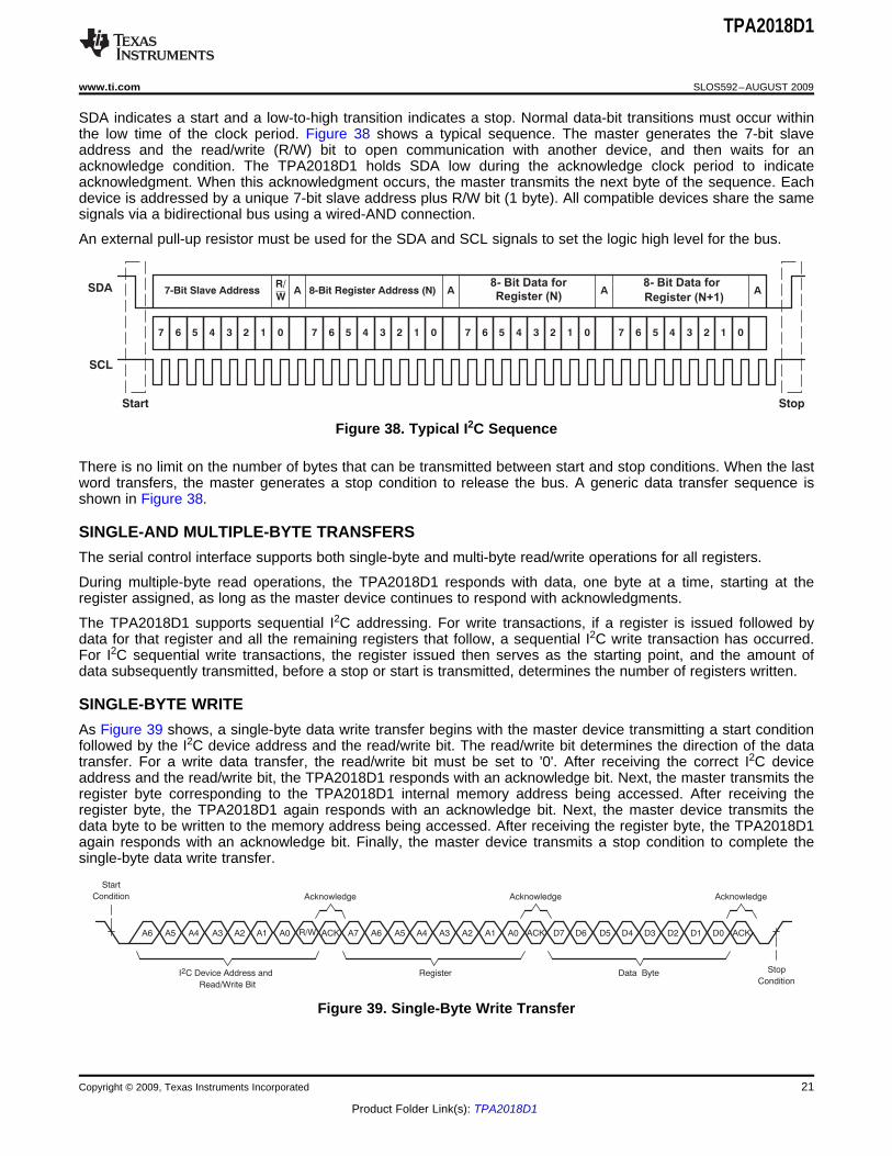
SDA indicates a start and a low-to-high transition indicates a stop. Normal data-bit transitions must occur withinthe low time of the clock period. Figure 38 shows a typical sequence. The master generates the 7-bit slaveaddress and the read/write (R/W) bit to open communication with another device, and then waits for anacknowledge condition. The TPA2018D1 holds SDA low during the acknowledge clock period to indicateacknowledgment. When this acknowledgment occurs, the master transmits the next byte of the sequence. Eachdevice is addressed by a unique 7-bit slave address plus R/W bit (1 byte). All compatible devices share the samesignals via a bidirectional bus using a wired-AND connection.
An external pull-up resistor must be used for the SDA and SCL signals to set the logic high level for the bus.
Figure 38. Typical I2C Sequence
There is no limit on the number of bytes that can be transmitted between start and stop conditions. When the lastword transfers, the master generates a stop condition to release the bus. A generic data transfer sequence isshown in Figure 38.
The serial control interface supports both single-byte and multi-byte read/write operations for all registers.
During multiple-byte read operations, the TPA2018D1 responds with data, one byte at a time, starting at theregister assigned, as long as the master device continues to respond with acknowledgments.
The TPA2018D1 supports sequential I2C addressing. For write transactions, if a register is issued followed bydata for that register and all the remaining registers that follow, a sequential I2C write transaction has occurred.For I2C sequential write transactions, the register issued then serves as the starting point, and the amount ofdata subsequently transmitted, before a stop or start is transmitted, determines the number of registers written.
As Figure 39 shows, a single-byte data write transfer begins with the master device transmitting a start conditionfollowed by the I2C device address and the read/write bit. The read/write bit determines the direction of the datatransfer. For a write data transfer, the read/write bit must be set to '0'. After receiving the correct I2C deviceaddress and the read/write bit, the TPA2018D1 responds with an acknowledge bit. Next, the master transmits theregister byte corresponding to the TPA2018D1 internal memory address being accessed. After receiving theregister byte, the TPA2018D1 again responds with an acknowledge bit. Next, the master device transmits thedata byte to be written to the memory address being accessed. After receiving the register byte, the TPA2018D1again responds with an acknowledge bit. Finally, the master device transmits a stop condition to complete thesingle-byte data write transfer.
Figure 39. Single-Byte Write Transfer
Copyright © 2009, Texas Instruments Incorporated 21
Product Folder Link(s): TPA2018D1
MULTIPLE-BYTE WRITE AND INCREMENTAL MULTIPLE-BYTE WRITE
Register
SINGLE-BYTE READ
A6 A5 A0 R/W ACK A7 A6 A5 A4 A0 ACK A6 A5 A0 ACK
Start
Condition
Stop
Condition
Acknowledge Acknowledge Acknowledge
I2C Device Address and
Read/Write Bit
Register Data Byte
D7 D6 D1 D0 ACK
I2C Device Address and
Read/Write Bit
Not
Acknowledge
R/WA1 A1
Repeat Start
Condition
MULTIPLE-BYTE READ
A6 A0 ACK
Acknowledge
I2C Device Address and
Read/Write Bit
R/WA6 A0 R/W ACK A0 ACK D7 D0 ACK
Start
Condition
Stop
Condition
Acknowledge Acknowledge Acknowledge
Last Data Byte
ACK
First Data Byte
Repeat Start
ConditionNot
Acknowledge
I2C Device Address and
Read/Write Bit
Register Other Data Bytes
A7 A6 A5 D7 D0 ACK
Acknowledge
D7 D0
TPA2018D1
SLOS592–AUGUST 2009 ................................................................................................................................................................................................ www.ti.com
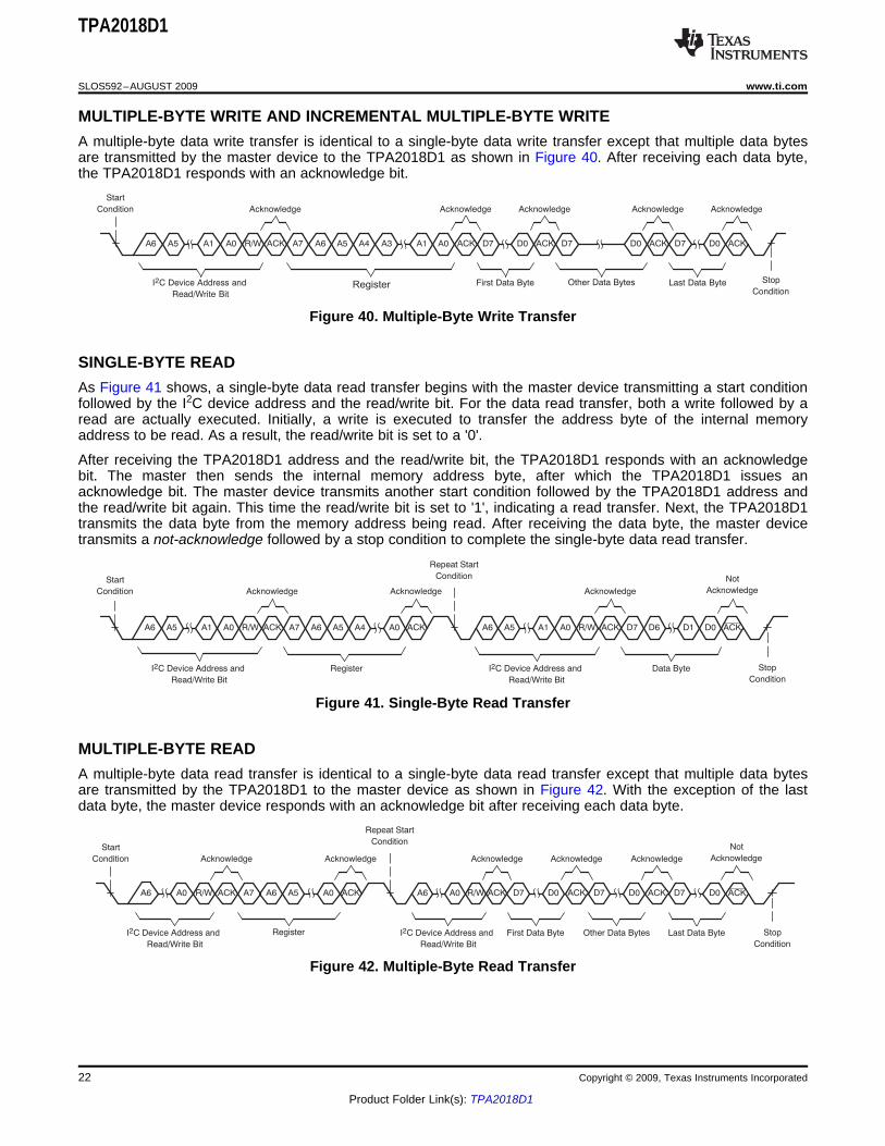
A multiple-byte data write transfer is identical to a single-byte data write transfer except that multiple data bytesare transmitted by the master device to the TPA2018D1 as shown in Figure 40. After receiving each data byte,the TPA2018D1 responds with an acknowledge bit.
Figure 40. Multiple-Byte Write Transfer
As Figure 41 shows, a single-byte data read transfer begins with the master device transmitting a start conditionfollowed by the I2C device address and the read/write bit. For the data read transfer, both a write followed by aread are actually executed. Initially, a write is executed to transfer the address byte of the internal memoryaddress to be read. As a result, the read/write bit is set to a '0'.
After receiving the TPA2018D1 address and the read/write bit, the TPA2018D1 responds with an acknowledgebit. The master then sends the internal memory address byte, after which the TPA2018D1 issues anacknowledge bit. The master device transmits another start condition followed by the TPA2018D1 address andthe read/write bit again. This time the read/write bit is set to '1', indicating a read transfer. Next, the TPA2018D1transmits the data byte from the memory address being read. After receiving the data byte, the master devicetransmits a not-acknowledge followed by a stop condition to complete the single-byte data read transfer.
Figure 41. Single-Byte Read Transfer
A multiple-byte data read transfer is identical to a single-byte data read transfer except that multiple data bytesare transmitted by the TPA2018D1 to the master device as shown in Figure 42. With the exception of the lastdata byte, the master device responds with an acknowledge bit after receiving each data byte.
Figure 42. Multiple-Byte Read Transfer
22 Copyright © 2009, Texas Instruments Incorporated
Product Folder Link(s): TPA2018D1
Register Map
TPA2018D1
www.ti.com ................................................................................................................................................................................................ SLOS592–AUGUST 2009
Table 3. TPA2018D1 Register MapRegister Bit7 Bit6 Bit5 Bit4 Bit3 Bit2 Bit1 Bit0
1 0 SPK_EN SWS 0 FAULT Thermal 1 NG_EN2 0 0 ATK_time [5] ATK_time [4] ATK_time [3] ATK_time [2] ATK_time [1] ATK_time [0]3 0 0 REL_time [5] REL_time [4] REL_time [3] REL_time [2] REL_time [1] REL_time [0]4 0 0 Hold_time [5] Hold_time [4] Hold_time [3] Hold_time [2] Hold_time [1] Hold_time [0]5 0 0 FixedGain [5] FixedGain [4] FixedGain [3] FixedGain [2] FixedGain [1] FixedGain [0]
Output NoiseGate NoiseGate Output Limiter Output Limiter Output Limiter Output Limiter Output Limiter6 Limiter Threshold Threshold [2] Level [4] Level [3] Level [2] Level [1] Level [0]Disable [1]Max Gain Max Gain Compression Compression7 Max Gain [1] Max Gain [0] 0 0[3] [2] Ratio [1] Ratio [0]
The default register map values are given in Table 4.
Table 4. TPA2018D1 Default Register Values TableRegister 0x01 0x02 0x03 0x04 0x05 0x06 0x07Default C3h 05h 0Bh 00h 06h 3Ah C2h
Any register above address 0x08 is reserved for testing and should not be written to because it may change thefunction of the device. If read, these bits may assume any value.
Some of the default values can be reprogrammed through the I2C interface and written to the EEPROM. Thisfunction is useful to speed up the turn-on time of the device and minimizes the number of I2C writes. If this isrequired, contact your local TI representative.
The TPA2018D1 I2C address is 0xB0 (binary 10110000) for writing and 0xB1 (binary 10110001) for reading. If adifferent I2C address is required, please contact your local TI representative. See the General I2C operationsection for more detail.
The following tables show the details of the registers, the default values, and the values that can be programmedthrough the I2C interface.
Copyright © 2009, Texas Instruments Incorporated 23
Product Folder Link(s): TPA2018D1

TPA2018D1
SLOS592–AUGUST 2009 ................................................................................................................................................................................................ www.ti.com
IC FUNCTION CONTROL (Address: 1)REGISTER I2C BIT LABEL DEFAULT DESCRIPTIONADDRESS01 (01H) – IC 7 Unused 1Function Control
6 SPK_EN 1 (enabled) Enables amplifier5 SWS 0 (enabled) Shutdown IC when bit = 14 Unused 03 FAULT 0 Changes to a 1 when there is a short on the left channel. Reset by writing a
02 Thermal 0 Changes to a 1 when die temperature is above 150°C1 Unused 10 NG_EN 1 (enabled) Enables Noise Gate function
SPK_EN: Enable bit for the audio amplifier channel. Amplifier is active when bit is high. This function isgated by thermal and returns once the IC is below the threshold temperature
SWS: Software shutdown control. The device is in software shutdown when the bit is '1' (control, biasand oscillator are inactive). When the bit is '0' the control, bias and oscillator are enabled.
Fault: This bit indicates that an over-current event has occurred on the channel with a '1'. This bit iscleared by writing a '0' to it.
Thermal: This bit indicates a thermal shutdown that was initiated by the hardware with a '1'. This bit isdeglitched and latched, and can be cleared by writing a '0' to it.
NG_EN: Enable bit for the Noise Gate function. This function is enabled when this bit is high. Thisfunction can only be enabled when the Compression ratio is not 1:1.
AGC ATTACK CONTROL (Address: 2)REGISTER I2C LABEL DEFAULT DESCRIPTIONADDRESS BIT
02 (02H) – 7:6 Unused 00AGC Control 5:0 ATK_time 000101 AGC Attack time (gain ramp down)
(6.4 ms/6 dB) Per Step Per 6 dB 90% Range000001 0.1067 ms 1.28 ms 5.76 ms000010 0.2134 ms 2.56 ms 11.52 ms000011 0.3201 ms 3.84 ms 17.19 ms000100 0.4268 ms 5.12 ms 23.04 ms
(time increases by 0.1067 ms with every step)111111 6.722 ms 80.66 ms 362.99 ms
ATK_time These bits set the attack time for the AGC function. The attack time is the minimum timebetween gain decreases.
24 Copyright © 2009, Texas Instruments Incorporated
Product Folder Link(s): TPA2018D1

TPA2018D1
www.ti.com ................................................................................................................................................................................................ SLOS592–AUGUST 2009
AGC RELEASE CONTROL (Address: 3)REGISTER I2C LABEL DEFAULT DESCRIPTIONADDRESS BIT
03 (03H) – 7:6 Unused 00AGC Release 5:0 REL_time 001011 AGC Release time (gain ramp down)Control (1.81 sec/6 dB) Per Step Per 6 dB 90% Range
000001 0.0137 s 0.1644 s 0.7398 s000010 0.0274 s 0.3288 s 1.4796 s000011 0.0411 s 0.4932 s 2.2194 s000100 0.0548 s 0.6576 s 2.9592 s
(time increases by 0.0137 s with every step)111111 0.8631 s 10.36 s 46.6 s
REL_time These bits set the release time for the AGC function. The release time is the minimum timebetween gain increases.
AGC HOLD TIME CONTROL (Address: 4)REGISTER I2C LABEL DEFAULT DESCRIPTIONADDRESS BIT
04 (04H) – 7:6 Unused 00AGC Hold 5:0 Hold_time 000000 (Disabled) AGC Hold timeTime Control
Per StepHold Time000000 Disable
000001 0.0137 s000010 0.0274 s000011 0.0411 s000100 0.0548 s
(time increases by 0.0137 s withevery step)
111111 0.8631 s
Hold_time These bits set the hold time for the AGC function. The hold time is the minimum time betweena gain decrease (attack) and a gain increase (release). The hold time can be deactivated.
Copyright © 2009, Texas Instruments Incorporated 25
Product Folder Link(s): TPA2018D1
TPA2018D1
SLOS592–AUGUST 2009 ................................................................................................................................................................................................ www.ti.com
AGC FIXED GAIN CONTROL (Address: 5)REGISTER I2C LABEL DEFAULT DESCRIPTIONADDRESS BIT
05 (05H) – 7:6 UNUSED 00AGC Fixed 5:0 Fixed Gain 00110 (6dB) Sets the fixed gain of the amplifier: two's complimentGain Control
Gain100100 –28 dB100101 –27 dB100110 –26 dB
(gain increases by 1 dB with every step)111101 –3 dB111110 –2 dB111111 –1 dB000000 0 dB000001 1 dB000010 2 dB000011 3 dB
(gain increases by 1dB with every step)011100 28 dB011101 29 dB011110 30 dB
Fixed Gain These bits are used to select the fixed gain of the amplifier. If the Compression is enabled,fixed gain is adjustable from –28dB to 30dB. If the Compression is disabled, fixed gain isadjustable from 0dB to 30dB.
26 Copyright © 2009, Texas Instruments Incorporated
Product Folder Link(s): TPA2018D1

TPA2018D1
www.ti.com ................................................................................................................................................................................................ SLOS592–AUGUST 2009
AGC CONTROL (Address: 6)REGISTER I2C LABEL DEFAULT DESCRIPTIONADDRESS BIT
06 (06H) – 7 Output Limiter 0 (enable) Disables the output limiter function. Can only be disabled when the AGCAGC Control Disable compression ratio is 1:1 (off)
6:5 NoiseGate 01 (4 mVrms) Select the threshold of the noise gateThreshold Threshold
00 1 mVrms
01 4 mVrms
10 10 mVrms
11 20 mVrms
4:0 Output Limiter 11010 (6.5dBV) Selects the output limiter levelLevel Output Power Peak Output dBV(Wrms) Voltage (Vp)
00000 0.03 0.67 –6.500001 0.03 0.71 –600010 0.04 0.75 –5.5
(Limiter level increases by 0.5dB with every step)11101 0.79 3.55 811110 0.88 3.76 8.511111 0.99 3.99 9
Output Limiter This bit disables the output limiter function when set to 1. Can only be disabled whenDisable the AGC compression ratio is 1:1NoiseGate Threshold These bits set the threshold level of the noise gate. NoiseGate Threshold is only
functional when the compression ratio is not 1:1Output Limiter Level These bits select the output limiter level. Output Power numbers are for 8Ω load.
AGC CONTROL (Address: 7)REGISTER I2C LABEL DEFAULT DESCRIPTIONADDRESS BIT
07 (07H) – 7:4 Max Gain 1100 (30 dB) Selects the maximum gain the AGC can achieveAGC Control Gain
0000 18 dB0001 19 dB0010 20 dB
(gain increases by 1 dB with every step)1100 30 dB
3:2 UNUSED 001:0 Compression 10 (4:1) Selects the compression ratio of the AGC
Ratio Ratio00 1:1 (off)01 2:110 4:111 8:1
Compression Ratio These bits select the compression ratio. Output Limiter is enabled by default when thecompression ratio is not 1:1.
Max Gain These bits select the maximum gain of the amplifier. In order to maximize the use of theAGC, set the Max Gain to 30dB
Copyright © 2009, Texas Instruments Incorporated 27
Product Folder Link(s): TPA2018D1

DECOUPLING CAPACITOR CS)
INPUT CAPACITORS CI)
CI I
1f =
(2 R C )p ´ ´
(5)
II C
1C =
(2 R f )p ´ ´
(6)
PACKAGE INFORMATION
Package Dimensions
BOARD LAYOUT
TPA2018D1
SLOS592–AUGUST 2009 ................................................................................................................................................................................................ www.ti.com
The TPA2018D1 is a high-performance Class-D audio amplifier that requires adequate power supply decouplingto ensure the efficiency is high and total harmonic distortion (THD) is low. For higher frequency transients,spikes, or digital hash on the line, a good low equivalent-series-resistance (ESR) 1-µF ceramic capacitor(typically) placed as close as possible to the device PVDD lead works best. Placing this decoupling capacitorclose to the TPA2018D1 is important for the efficiency of the Class-D amplifier, because any resistance orinductance in the trace between the device and the capacitor can cause a loss in efficiency. For filteringlower-frequency noise signals, a 4.7 µF or greater capacitor placed near the audio power amplifier would alsohelp, but it is not required in most applications because of the high PSRR of this device.
TPA2018D1 requires input capacitors to ensure low output offset and low pop.The input capacitors and input resistors form a high-pass filter with the corner frequency, fC, determined inEquation 5.
The value of the input capacitor is important to consider as it directly affects the bass (low frequency)performance of the circuit. Speakers in wireless phones cannot usually respond well to low frequencies, so thecorner frequency can be set to block low frequencies in this application. Not using input capacitors can increaseoutput offset. Equation 6 is used to solve for the input coupling capacitance. If the corner frequency is within theaudio band, the capacitors should have a tolerance of ±10% or better, because any mismatch in capacitancecauses an impedance mismatch at the corner frequency and below.
The package dimensions for this YZF package are shown in the table below. See the package drawing at theend of this data sheet for more details.
Table 5. YZF Package DimensionsPackaged Devices D E
Min = 1594µm Min = 1594µmTPA2018D1YZF Max = 1654µm Max = 1654µm
In making the pad size for the WCSP balls, it is recommended that the layout use non solder mask defined(NSMD) land. With this method, the solder mask opening is made larger than the desired land area, and theopening size is defined by the copper pad width. Figure 43 and Table 6 shows the appropriate diameters for aWCSP layout. The TPA2018D1 evaluation module (EVM) layout is shown in the next section as a layoutexample.
28 Copyright © 2009, Texas Instruments Incorporated
Product Folder Link(s): TPA2018D1
COMPONENT LOCATION
TRACE WIDTH
TPA2018D1
www.ti.com ................................................................................................................................................................................................ SLOS592–AUGUST 2009
Figure 43. Land Pattern Dimensions
Table 6. Land Pattern Dimensions (1) (2) (3) (4)
SOLDER PAD SOLDER MASK (5) COPPER STENCILCOPPER PAD STENCIL (6) (7) OPENINGDEFINITIONS OPENING THICKNESS THICKNESS275 µm 375 µmNon solder mask 275 µm × 275 µm Sq. (rounded1 oz max (32 µm) 125 µm thickdefined (NSMD) corners)(+0.0, –25 µm) (+0.0, –25 µm)
(1) Circuit traces from NSMD defined PWB lands should be 75 µm to 100 µm wide in the exposed area inside the solder mask opening.Wider trace widths reduce device stand off and impact reliability.
(2) Best reliability results are achieved when the PWB laminate glass transition temperature is above the operating the range of theintended application.
(3) Recommend solder paste is Type 3 or Type 4.(4) For a PWB using a Ni/Au surface finish, the gold thickness should be less 0.5 mm to avoid a reduction in thermal fatigue performance.(5) Solder mask thickness should be less than 20 µm on top of the copper circuit pattern(6) Best solder stencil performance is achieved using laser cut stencils with electro polishing. Use of chemically etched stencils results in
inferior solder paste volume control.(7) Trace routing away from WCSP device should be balanced in X and Y directions to avoid unintentional component movement due to
solder wetting forces.
Place all the external components very close to the TPA2018D1. Placing the decoupling capacitor, CS, close tothe TPA2018D1 is important for the efficiency of the Class-D amplifier. Any resistance or inductance in the tracebetween the device and the capacitor can cause a loss in efficiency.
Recommended trace width at the solder balls is 75 µm to 100 µm to prevent solder wicking onto wider PCBtraces. For high current pins (PVDD (L, R), PGND, and audio output pins) of the TPA2018D1, use 100-µm tracewidths at the solder balls and at least 500-µm PCB traces to ensure proper performance and output power forthe device. For the remaining signals of the TPA2018D1, use 75-µm to 100-µm trace widths at the solder balls.The audio input pins (INR± and INL±) must run side-by-side to maximize common-mode noise cancellation
Copyright © 2009, Texas Instruments Incorporated 29
Product Folder Link(s): TPA2018D1
EFFICIENCY AND THERMAL INFORMATION
105°C/W
(7)
A J JA DMAXT Max = T Max - θ P = 150 - 105 (0.4) = 108°C(8)
OPERATION WITH DACS AND CODECS
SHORT CIRCUIT AUTO-RECOVERY
FILTER FREE OPERATION AND FERRITE BEAD FILTERS
FerriteChip Bead
FerriteChip Bead
1 nF
1 nF
OUTP
OUTN
TPA2018D1
SLOS592–AUGUST 2009 ................................................................................................................................................................................................ www.ti.com
The maximum ambient temperature depends on the heat-sinking ability of the PCB system. The derating factorfor the packages are shown in the dissipation rating table. Converting this to θJA for the WCSP package:
Given θJA of 105°C/W, the maximum allowable junction temperature of 150°C, and the maximum internaldissipation of 0.4 W for 3 W output power, 4-Ω load, 5-V supply, from Figure 17, the maximum ambienttemperature can be calculated with the following equation.
Equation 8 shows that the calculated maximum ambient temperature is 108°C at maximum power dissipationwith a 5-V supply and 4-Ω a load. The TPA2018D1 is designed with thermal protection that turns the device offwhen the junction temperature surpasses 150°C to prevent damage to the IC. Also, using speakers moreresistive than 8-Ω dramatically increases the thermal performance by reducing the output current and increasingthe efficiency of the amplifier.
In using Class-D amplifiers with CODECs and DACs, sometimes there is an increase in the output noise floorfrom the audio amplifier. This occurs when mixing of the output frequencies of the CODEC/DAC mix with theswitching frequencies of the audio amplifier input stage. The noise increase can be solved by placing a low-passfilter between the CODEC/DAC and audio amplifier. This filters off the high frequencies that cause the problemand allow proper performance. See the functional block diagram.
When a short circuit event happens, the TPA2018D1 goes to shutdown mode and tries to reactivate itself every 5ms. This auto-recovery will continue until the short circuit event stops. This feature can protect the device withoutaffecting the device's long term reliability. FAULT bit (register 1, bit 3) still requires a write to clear.
A ferrite bead filter can often be used if the design is failing radiated emissions without an LC filter and thefrequency sensitive circuit is greater than 1 MHz. This filter functions well for circuits that just have to pass FCCand CE because FCC and CE only test radiated emissions greater than 30 MHz. When choosing a ferrite bead,choose one with high impedance at high frequencies, and low impedance at low frequencies. In addition, select aferrite bead with adequate current rating to prevent distortion of the output signal.
Use an LC output filter if there are low frequency (< 1 MHz) EMI sensitive circuits and/or there are long leadsfrom amplifier to speaker. Figure 44 shows typical ferrite bead and LC output filters.
Figure 44. Typical Ferrite Bead Filter (Chip bead example: TDK: MPZ1608S221A)
30 Copyright © 2009, Texas Instruments Incorporated
Product Folder Link(s): TPA2018D1
TPA2018D1
www.ti.com ................................................................................................................................................................................................ SLOS592–AUGUST 2009
Figure 45. EMC Performance under FCC Class-B
Figure 45 shows the EMC performance of TPA2018D1 under FCC Class-B. The test circuit configuration isshown in Figure 44. The worst-case quasi peak margin is 29.8 dB at 30.5 MHz.
Table 7. Measurement Condition for TPA2018D1 EMC TestPARAMETER VALUE UNIT
VDD Supply voltage 4.2 VAV Gain 6 dBfAUD Input signal frequency 1 kHzVI Input signal amplitude 1 VRMS
VO Output signal amplitude 2 VRMS
RL Load impedance 8 ΩOutput cable length 100 mm
Copyright © 2009, Texas Instruments Incorporated 31
Product Folder Link(s): TPA2018D1

PACKAGE OPTION ADDENDUM
www.ti.com 11-Apr-2013
Addendum-Page 1
PACKAGING INFORMATION
Orderable Device Status(1)
Package Type PackageDrawing
Pins PackageQty
Eco Plan(2)
Lead/Ball Finish MSL Peak Temp(3)
Op Temp (°C) Top-Side Markings(4)
Samples
TPA2018D1YZFR ACTIVE DSBGA YZF 9 3000 Green (RoHS& no Sb/Br)
SNAGCU Level-1-260C-UNLIM -40 to 85 OBC
TPA2018D1YZFT ACTIVE DSBGA YZF 9 250 Green (RoHS& no Sb/Br)
SNAGCU Level-1-260C-UNLIM -40 to 85 OBC
(1) The marketing status values are defined as follows:ACTIVE: Product device recommended for new designs.LIFEBUY: TI has announced that the device will be discontinued, and a lifetime-buy period is in effect.NRND: Not recommended for new designs. Device is in production to support existing customers, but TI does not recommend using this part in a new design.PREVIEW: Device has been announced but is not in production. Samples may or may not be available.OBSOLETE: TI has discontinued the production of the device.
(2) Eco Plan - The planned eco-friendly classification: Pb-Free (RoHS), Pb-Free (RoHS Exempt), or Green (RoHS & no Sb/Br) - please check http://www.ti.com/productcontent for the latest availabilityinformation and additional product content details.TBD: The Pb-Free/Green conversion plan has not been defined.Pb-Free (RoHS): TI's terms "Lead-Free" or "Pb-Free" mean semiconductor products that are compatible with the current RoHS requirements for all 6 substances, including the requirement thatlead not exceed 0.1% by weight in homogeneous materials. Where designed to be soldered at high temperatures, TI Pb-Free products are suitable for use in specified lead-free processes.Pb-Free (RoHS Exempt): This component has a RoHS exemption for either 1) lead-based flip-chip solder bumps used between the die and package, or 2) lead-based die adhesive used betweenthe die and leadframe. The component is otherwise considered Pb-Free (RoHS compatible) as defined above.Green (RoHS & no Sb/Br): TI defines "Green" to mean Pb-Free (RoHS compatible), and free of Bromine (Br) and Antimony (Sb) based flame retardants (Br or Sb do not exceed 0.1% by weightin homogeneous material)
(3) MSL, Peak Temp. -- The Moisture Sensitivity Level rating according to the JEDEC industry standard classifications, and peak solder temperature.
(4) Multiple Top-Side Markings will be inside parentheses. Only one Top-Side Marking contained in parentheses and separated by a "~" will appear on a device. If a line is indented then it is acontinuation of the previous line and the two combined represent the entire Top-Side Marking for that device.
Important Information and Disclaimer:The information provided on this page represents TI's knowledge and belief as of the date that it is provided. TI bases its knowledge and belief on informationprovided by third parties, and makes no representation or warranty as to the accuracy of such information. Efforts are underway to better integrate information from third parties. TI has taken andcontinues to take reasonable steps to provide representative and accurate information but may not have conducted destructive testing or chemical analysis on incoming materials and chemicals.TI and TI suppliers consider certain information to be proprietary, and thus CAS numbers and other limited information may not be available for release.
In no event shall TI's liability arising out of such information exceed the total purchase price of the TI part(s) at issue in this document sold by TI to Customer on an annual basis.

TAPE AND REEL INFORMATION
*All dimensions are nominal
Device PackageType
PackageDrawing
Pins SPQ ReelDiameter
(mm)
ReelWidth
W1 (mm)
A0(mm)
B0(mm)
K0(mm)
P1(mm)
W(mm)
Pin1Quadrant
TPA2018D1YZFR DSBGA YZF 9 3000 180.0 8.4 1.71 1.71 0.81 4.0 8.0 Q1
TPA2018D1YZFT DSBGA YZF 9 250 180.0 8.4 1.71 1.71 0.81 4.0 8.0 Q1
PACKAGE MATERIALS INFORMATION
www.ti.com 13-May-2016
Pack Materials-Page 1

*All dimensions are nominal
Device Package Type Package Drawing Pins SPQ Length (mm) Width (mm) Height (mm)
TPA2018D1YZFR DSBGA YZF 9 3000 210.0 185.0 35.0
TPA2018D1YZFT DSBGA YZF 9 250 210.0 185.0 35.0
PACKAGE MATERIALS INFORMATION
www.ti.com 13-May-2016
Pack Materials-Page 2

D: Max =
E: Max =
1.655 mm, Min =
1.655 mm, Min =
1.594 mm
1.594 mm
IMPORTANT NOTICE
Texas Instruments Incorporated (TI) reserves the right to make corrections, enhancements, improvements and other changes to itssemiconductor products and services per JESD46, latest issue, and to discontinue any product or service per JESD48, latest issue. Buyersshould obtain the latest relevant information before placing orders and should verify that such information is current and complete.TI’s published terms of sale for semiconductor products (http://www.ti.com/sc/docs/stdterms.htm) apply to the sale of packaged integratedcircuit products that TI has qualified and released to market. Additional terms may apply to the use or sale of other types of TI products andservices.Reproduction of significant portions of TI information in TI data sheets is permissible only if reproduction is without alteration and isaccompanied by all associated warranties, conditions, limitations, and notices. TI is not responsible or liable for such reproduceddocumentation. Information of third parties may be subject to additional restrictions. Resale of TI products or services with statementsdifferent from or beyond the parameters stated by TI for that product or service voids all express and any implied warranties for theassociated TI product or service and is an unfair and deceptive business practice. TI is not responsible or liable for any such statements.Buyers and others who are developing systems that incorporate TI products (collectively, “Designers”) understand and agree that Designersremain responsible for using their independent analysis, evaluation and judgment in designing their applications and that Designers havefull and exclusive responsibility to assure the safety of Designers' applications and compliance of their applications (and of all TI productsused in or for Designers’ applications) with all applicable regulations, laws and other applicable requirements. Designer represents that, withrespect to their applications, Designer has all the necessary expertise to create and implement safeguards that (1) anticipate dangerousconsequences of failures, (2) monitor failures and their consequences, and (3) lessen the likelihood of failures that might cause harm andtake appropriate actions. Designer agrees that prior to using or distributing any applications that include TI products, Designer willthoroughly test such applications and the functionality of such TI products as used in such applications.TI’s provision of technical, application or other design advice, quality characterization, reliability data or other services or information,including, but not limited to, reference designs and materials relating to evaluation modules, (collectively, “TI Resources”) are intended toassist designers who are developing applications that incorporate TI products; by downloading, accessing or using TI Resources in anyway, Designer (individually or, if Designer is acting on behalf of a company, Designer’s company) agrees to use any particular TI Resourcesolely for this purpose and subject to the terms of this Notice.TI’s provision of TI Resources does not expand or otherwise alter TI’s applicable published warranties or warranty disclaimers for TIproducts, and no additional obligations or liabilities arise from TI providing such TI Resources. TI reserves the right to make corrections,enhancements, improvements and other changes to its TI Resources. TI has not conducted any testing other than that specificallydescribed in the published documentation for a particular TI Resource.Designer is authorized to use, copy and modify any individual TI Resource only in connection with the development of applications thatinclude the TI product(s) identified in such TI Resource. NO OTHER LICENSE, EXPRESS OR IMPLIED, BY ESTOPPEL OR OTHERWISETO ANY OTHER TI INTELLECTUAL PROPERTY RIGHT, AND NO LICENSE TO ANY TECHNOLOGY OR INTELLECTUAL PROPERTYRIGHT OF TI OR ANY THIRD PARTY IS GRANTED HEREIN, including but not limited to any patent right, copyright, mask work right, orother intellectual property right relating to any combination, machine, or process in which TI products or services are used. Informationregarding or referencing third-party products or services does not constitute a license to use such products or services, or a warranty orendorsement thereof. Use of TI Resources may require a license from a third party under the patents or other intellectual property of thethird party, or a license from TI under the patents or other intellectual property of TI.TI RESOURCES ARE PROVIDED “AS IS” AND WITH ALL FAULTS. TI DISCLAIMS ALL OTHER WARRANTIES ORREPRESENTATIONS, EXPRESS OR IMPLIED, REGARDING RESOURCES OR USE THEREOF, INCLUDING BUT NOT LIMITED TOACCURACY OR COMPLETENESS, TITLE, ANY EPIDEMIC FAILURE WARRANTY AND ANY IMPLIED WARRANTIES OFMERCHANTABILITY, FITNESS FOR A PARTICULAR PURPOSE, AND NON-INFRINGEMENT OF ANY THIRD PARTY INTELLECTUALPROPERTY RIGHTS. TI SHALL NOT BE LIABLE FOR AND SHALL NOT DEFEND OR INDEMNIFY DESIGNER AGAINST ANY CLAIM,INCLUDING BUT NOT LIMITED TO ANY INFRINGEMENT CLAIM THAT RELATES TO OR IS BASED ON ANY COMBINATION OFPRODUCTS EVEN IF DESCRIBED IN TI RESOURCES OR OTHERWISE. IN NO EVENT SHALL TI BE LIABLE FOR ANY ACTUAL,DIRECT, SPECIAL, COLLATERAL, INDIRECT, PUNITIVE, INCIDENTAL, CONSEQUENTIAL OR EXEMPLARY DAMAGES INCONNECTION WITH OR ARISING OUT OF TI RESOURCES OR USE THEREOF, AND REGARDLESS OF WHETHER TI HAS BEENADVISED OF THE POSSIBILITY OF SUCH DAMAGES.Unless TI has explicitly designated an individual product as meeting the requirements of a particular industry standard (e.g., ISO/TS 16949and ISO 26262), TI is not responsible for any failure to meet such industry standard requirements.Where TI specifically promotes products as facilitating functional safety or as compliant with industry functional safety standards, suchproducts are intended to help enable customers to design and create their own applications that meet applicable functional safety standardsand requirements. Using products in an application does not by itself establish any safety features in the application. Designers mustensure compliance with safety-related requirements and standards applicable to their applications. Designer may not use any TI products inlife-critical medical equipment unless authorized officers of the parties have executed a special contract specifically governing such use.Life-critical medical equipment is medical equipment where failure of such equipment would cause serious bodily injury or death (e.g., lifesupport, pacemakers, defibrillators, heart pumps, neurostimulators, and implantables). Such equipment includes, without limitation, allmedical devices identified by the U.S. Food and Drug Administration as Class III devices and equivalent classifications outside the U.S.TI may expressly designate certain products as completing a particular qualification (e.g., Q100, Military Grade, or Enhanced Product).Designers agree that it has the necessary expertise to select the product with the appropriate qualification designation for their applicationsand that proper product selection is at Designers’ own risk. Designers are solely responsible for compliance with all legal and regulatoryrequirements in connection with such selection.Designer will fully indemnify TI and its representatives against any damages, costs, losses, and/or liabilities arising out of Designer’s non-compliance with the terms and provisions of this Notice.
Mailing Address: Texas Instruments, Post Office Box 655303, Dallas, Texas 75265Copyright © 2018, Texas Instruments Incorporated