lm4680 10w high-efficiency mono btl audio power · pdf filelm4680 10w high-efficiency mono btl...
TRANSCRIPT
LM4680
LM4680 10W High-Efficiency Mono BTL Audio Power Amplifier
Literature Number: SNAS246

LM468010W High-Efficiency Mono BTL Audio Power AmplifierGeneral DescriptionThe LM4680 is a high efficiency switching audio poweramplifier primarily designed for demanding applications inflat panel monitors and TV’s. It is capable of delivering 10Wto an 8Ω mono BTL load with less than 10% distortion(THD+N) when powered from a 14VDC power supply.
Boomer audio power amplifiers were designed specifically toprovide high quality output power with a minimal amount ofexternal components. The LM4680 features a micro-power,active-low shutdown mode, an internal thermal shutdownprotection mechanism, output fault detect, and short circuitprotection.
The LM4680 contains advanced transient (“pop and click”)suppression circuitry that eliminates noises that would oth-erwise occur during turn-on and turn-off transitions.
Key Specificationsj Power Output BTL (VDD = 14V,
fIN = 1kHz, THD+N = 10%,RL = 8Ω) 10W (typ)
j Quiescent Power Supply Current 25mA (typ)
j Efficiency (VDD = 12V, fIN = 1kHz,RL = 8Ω, POUT = 6W) 81% (typ)
j Shutdown Current 0.1mA (typ)
j Fixed Gain 30dB (typ)
Featuresn Soft-start circuitry eliminates noise during turn-on
transitionn Low current shutdown moden Low quiescent currentn 6W BTL output, RL = 8Ω, THD+N = 1%n Short circuit protectionn Fixed, internally set gain of 30dBn Internal clamp diodes protect amplifier outputs
Applicationsn Flat Panel Monitorsn Flat Panel TVsn Computer Sound Cards
Connection DiagramPlastic Package
20095802
Top ViewOrder Number LM4680SD
See NS Package Number SRC14A
Boomer® is a registered trademark of National Semiconductor Corporation.
January 2005LM
468010W
High-E
fficiencyM
onoB
TLA
udioP
ower
Am
plifier
© 2005 National Semiconductor Corporation DS200958 www.national.com
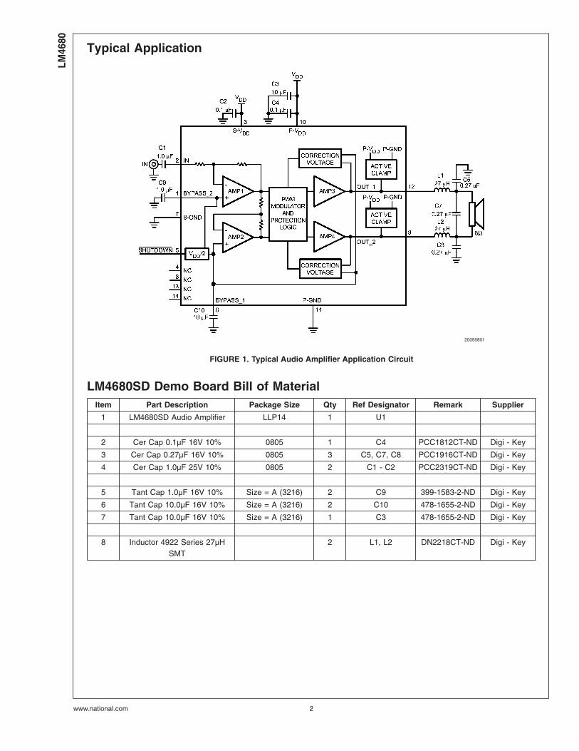
Typical Application
LM4680SD Demo Board Bill of MaterialItem Part Description Package Size Qty Ref Designator Remark Supplier
1 LM4680SD Audio Amplifier LLP14 1 U1
2 Cer Cap 0.1µF 16V 10% 0805 1 C4 PCC1812CT-ND Digi - Key
3 Cer Cap 0.27µF 16V 10% 0805 3 C5, C7, C8 PCC1916CT-ND Digi - Key
4 Cer Cap 1.0µF 25V 10% 0805 2 C1 - C2 PCC2319CT-ND Digi - Key
5 Tant Cap 1.0µF 16V 10% Size = A (3216) 2 C9 399-1583-2-ND Digi - Key
6 Tant Cap 10.0µF 16V 10% Size = A (3216) 2 C10 478-1655-2-ND Digi - Key
7 Tant Cap 10.0µF 16V 10% Size = A (3216) 1 C3 478-1655-2-ND Digi - Key
8 Inductor 4922 Series 27µHSMT
2 L1, L2 DN2218CT-ND Digi - Key
20095801
FIGURE 1. Typical Audio Amplifier Application Circuit
LM46
80
www.national.com 2
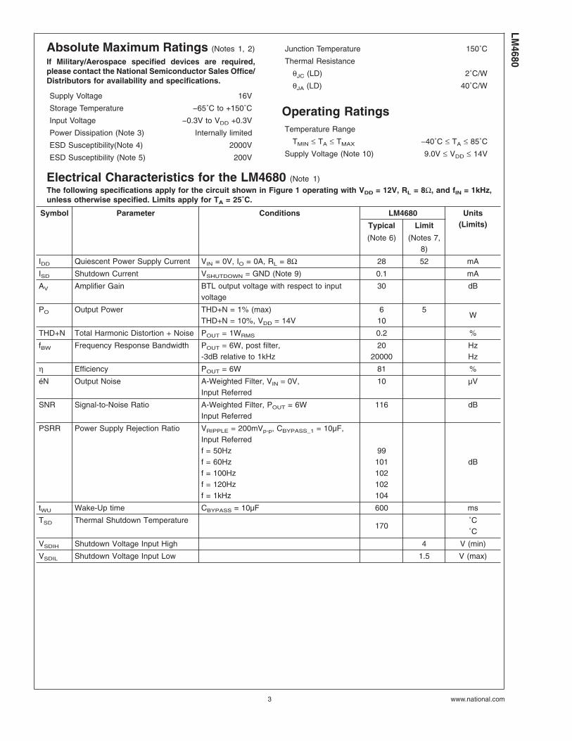
Absolute Maximum Ratings (Notes 1, 2)
If Military/Aerospace specified devices are required,please contact the National Semiconductor Sales Office/Distributors for availability and specifications.
Supply Voltage 16V
Storage Temperature −65˚C to +150˚C
Input Voltage −0.3V to VDD +0.3V
Power Dissipation (Note 3) Internally limited
ESD Susceptibility(Note 4) 2000V
ESD Susceptibility (Note 5) 200V
Junction Temperature 150˚C
Thermal Resistance
θJC (LD) 2˚C/W
θJA (LD) 40˚C/W
Operating RatingsTemperature Range
TMIN ≤ TA ≤ TMAX −40˚C ≤ TA ≤ 85˚C
Supply Voltage (Note 10) 9.0V ≤ VDD ≤ 14V
Electrical Characteristics for the LM4680 (Note 1)
The following specifications apply for the circuit shown in Figure 1 operating with VDD = 12V, RL = 8Ω, and fIN = 1kHz,unless otherwise specified. Limits apply for TA = 25˚C.
Symbol Parameter Conditions LM4680 Units(Limits)Typical Limit
(Note 6) (Notes 7,8)
IDD Quiescent Power Supply Current VIN = 0V, IO = 0A, RL = 8Ω 28 52 mA
ISD Shutdown Current VSHUTDOWN = GND (Note 9) 0.1 mA
AV Amplifier Gain BTL output voltage with respect to inputvoltage
30 dB
PO Output Power THD+N = 1% (max)THD+N = 10%, VDD = 14V
610
5W
THD+N Total Harmonic Distortion + Noise POUT = 1WRMS 0.2 %
fBW Frequency Response Bandwidth POUT = 6W, post filter,-3dB relative to 1kHz
2020000
HzHz
η Efficiency POUT = 6W 81 %
éN Output Noise A-Weighted Filter, VIN = 0V,Input Referred
10 µV
SNR Signal-to-Noise Ratio A-Weighted Filter, POUT = 6WInput Referred
116 dB
PSRR Power Supply Rejection Ratio VRIPPLE = 200mVp-p, CBYPASS_1 = 10µF,Input Referredf = 50Hzf = 60Hzf = 100Hzf = 120Hzf = 1kHz
99101102102104
dB
tWU Wake-Up time CBYPASS = 10µF 600 ms
TSD Thermal Shutdown Temperature170
˚C˚C
VSDIH Shutdown Voltage Input High 4 V (min)
VSDIL Shutdown Voltage Input Low 1.5 V (max)
LM4680
www.national.com3
Note 1: All voltages are measured with respect to the GND pin unless otherwise specified.
Note 2: Absolute Maximum Ratings indicate limits beyond which damage to the device may occur. Operating Ratings indicate conditions for which the device isfunctional, but do not guarantee specific performance limits. Electrical Characteristics state DC and AC electrical specifications under particular test conditions whichguarantee specific performance limits. This assumes that the device is within the Operating Ratings. Specifications are not guaranteed for parameters where no limitis given, however, the typical value is a good indication of device performance.
Note 3: The maximum power dissipation must be derated at elevated temperatures and is dictated by TJMAX, θJA, and the ambient temperature TA. The maximumallowable power dissipation is PDMAX = (TJMAX − TA)/θJA or the number given in Absolute Maximum Ratings, whichever is lower. For the LM4680 typical application(shown in Figure 1) with VDD = 12V, RL = 8Ω stereo operation, the total power dissipation is 900mW. θJA = 40˚C/W
Note 4: Human body model, 100pF discharged through a 1.5kΩ resistor.
Note 5: Machine model, 220pF – 240pF discharged through all pins.
Note 6: Typicals are measured at 25˚C and represent the parametric norm.
Note 7: Limits are guaranteed to National’s AOQL (Average Outgoing Quality Level).
Note 8: Datasheets min/max specification limits are guaranteed by design, test, or statistical analysis.
Note 9: Shutdown current is measured in a normal room environment. The SHUTDOWN pin should be driven as close as possible to GND for minimum shutdowncurrent.
Note 10: Please refer to “Under Voltage Protection” on page 8 under “General Features.”
Typical Performance CharacteristicsTHD+N vs Frequency
VDD = 9V, RL = 8Ω, PO = 1WTHD+N vs Frequency
VDD = 12V, RL = 8Ω, PO = 1W
20095806 20095807
THD+N vs FrequencyVDD = 14V, RL = 8Ω, PO = 1W
THD+N vs Output PowerRL = 8Ω, VDD = 9V, f = 1kHz
20095808 20095809
LM46
80
www.national.com 4
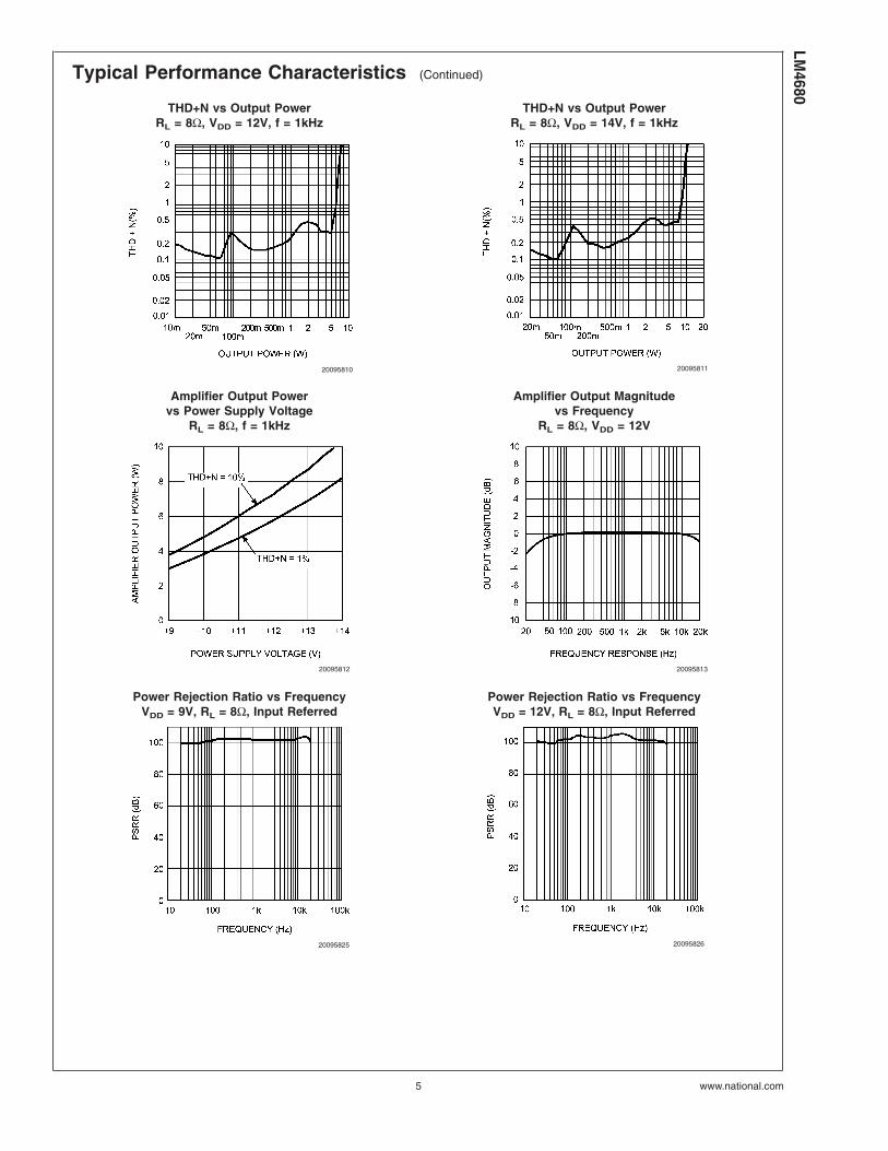
Typical Performance Characteristics (Continued)
THD+N vs Output PowerRL = 8Ω, VDD = 12V, f = 1kHz
THD+N vs Output PowerRL = 8Ω, VDD = 14V, f = 1kHz
20095810 20095811
Amplifier Output Powervs Power Supply Voltage
RL = 8Ω, f = 1kHz
Amplifier Output Magnitudevs Frequency
RL = 8Ω, VDD = 12V
20095812 20095813
Power Rejection Ratio vs FrequencyVDD = 9V, RL = 8Ω, Input Referred
Power Rejection Ratio vs FrequencyVDD = 12V, RL = 8Ω, Input Referred
20095825 20095826
LM4680
www.national.com5

Typical Performance Characteristics (Continued)
Power Rejection Ratio vs FrequencyVDD = 14V, RL = 8Ω, Input Referred
Amplifier Power Dissipationvs Amplifier Load DissipationVDD = 14V, RL = 8Ω, f = 1kHz
2009582720095817
Amplifier Power Dissipationvs Load Power Dissipation
VDD = 12V, RL = 8Ω, f = 1kHz
Amplifier Power Dissipationvs Total Load Power Dissipation
VDD = 9V, RL = 8Ω, f = 1kHz
20095818 20095819
Output Powervs Load ResistanceVDD = 14V, f = 1kHz
Output Powervs Load ResistanceVDD = 12V, f = 1kHz
20095820 20095821
LM46
80
www.national.com 6

Typical Performance Characteristics (Continued)
Output Powervs Load ResistanceVDD = 9V, f = 1kHz
Power Supply Currentvs Power Supply Voltage
VIN = 0V, RL = 8Ω
20095822 20095823
Power Dissipationvs Ambient Temperature
20095824
LM4680
www.national.com7
General Features
SYSTEM FUNCTIONAL INFORMATION
Modulation Technique
Unlike typical Class D amplifiers that use single-ended com-parators to generate a pulse-width modulated switchingwaveform and RC timing circuits to set the switching fre-quency, the LM4680 uses a balanced differential floatingmodulator. Oscillation is a result of injecting complimentarycurrents onto the respective plates of a floating, on-die ca-pacitor. The value of the floating capacitor and value of thecomponents in the modulator’s feedback network and setsthe nominal switching frequency at 450kHz. Modulation re-sults from imbalances in the injected currents. The amountof current imbalance is directly proportional to the appliedinput signal’s magnitude and frequency.
Using a balanced, floating modulator produces a Class Damplifier that is immune to common mode noise sourcessuch as substrate noise. This noise occurs because of thehigh frequency, high current switching in the amplifier’s out-put stage. The LM4680 is immune to this type of noisebecause the modulator, the components that set its switch-ing frequency, and even the load all float with respect toground.
The balanced modulator’s pulse width modulated outputdrives the gates of the LM4680’s H-bridge configured outputpower MOSFETs. The pulse-train present at the powerMOSFETs’ output is applied to an LC low pass filter thatremoves the 450kHz energy component. The filter’s outputsignal, which is applied to the driven load, is an amplifiedreplica of the audio input signal.
Shutdown Function
The LM4680’s active-low shutdown function allows the userto place the amplifier in a shutdown mode while the systempower supply remains active. Activating shutdown deacti-vates the output switching waveform and minimizes thequiescent current. Applying logic 0 (GND) to pin 8 enablesthe shutdown function. Applying logic 1 (4V ≤ VLOGIC ≤ VDD)to pin 8 disables the shutdown function and restores fullamplifier operation.
Under Voltage Proctection
The under voltage protection disables the output driver sec-tion of the LM4680 while the supply voltage is below 8V. Thiscondition may occur as power is first applied or during lowline conditions, changes in load resistance, or when powersupply sag occurs. The under voltage protection ensuresthat all of the LM4680’s power MOSFETs are off. This actioneliminates shoot-through current and minimizes output tran-sients during turn-on and turn-off. The under voltage protec-tion gives the digital logic time to stabilize into known states,further minimizing turn output transients.
Turn-On Time
The LM4680 has an internal timer that determines the am-plifier’s turn-on time. After power is first applied or the partreturns from shutdown, the nominal turn-on time is 600ms.This delay allows all externally applied capacitors to chargeto a final value of VDD/2. Further, during turn-on, the outputsare muted. This minimizes output transients that may occurwhile the part settles into is quiescent operating mode.
Output Stage Current Limit and Fault DetectionProtection
The output stage MOSFETs are protected against outputconditions that could otherwise compromise their operationalstatus. The first stage of protection is output current limiting.When conditions that require high currents to drive a load,the LM4680’s current limit circuitry clamps the output currentat a nominal value of 2.5A. The output waveform is present,but may be clipped or its amplitude reduced. The same 2.5Anominal current limit also occurs if the amplifier outputs areshorted together or either output is shorted to VDD or GND.
The second stage of protection is an onboard fault detectioncircuit that continuously monitors the signal on each outputMOSFET’s gate and compares it against the respectivedrain voltage. When a condition is detected that violates aMOSFET’s Safe Operating Area (SOA) and the drive signalis disconnected from the output MOSFETs’ gates. The faultdetect circuit maintains this protective condition for approxi-mately 600ms, at which time the drive signal is reconnected.If the fault condition is no longer present, normal operationresumes. If the fault condition remains, however, the drivesignal is again disconnected.
Thermal Protection
The LM4680 has thermal shutdown circuitry that monitorsthe die temperature. Once the LM4680 die temperaturereaches 170˚C, the LM4680 disables the output switchingwaveform and remains disabled until the die temperaturefalls below 140˚C (typ).
Over-Modulation Protection
The LM4680’s over-modulation protection is a result of thepreamplifier’s (AMP1 and AMP2, Figure 1) inability to pro-duce signal magnitudes that equal the power supply volt-ages. Since the preamplifier’s output magnitude will alwaysbe less than the supply voltage, the duty cycle of the ampli-fier’s switching output will never reach zero. Peak modula-tion is limited to a nominal 95%.
Application Hints
SUPPLY BYPASSING
Correct power supply bypassing has two important goals.The first is to reduce noise on the power supply lines andminimize deleterious effects that the noise may cause to theamplifier’s operation. The second is to help stabilize anunregulated power supply and to improve the supply’s tran-sient response under heavy current demands. These twogoals require different capacitor value ranges. Therefore,various types and values are recommended for supply by-passing. For noise de-coupling, generally small ceramic ca-pacitors (0.01µF to 0.1µF) are recommended. Larger value(1µF to 10µF) tantalum capacitors are needed for the tran-sient current demands. These two capacitors in parallel willdo an adequate job of removing most noise from the supplyrails and providing the necessary transient current. Thesecapacitors should be placed as close as possible to eachIC’s supply pin(s) using leads as short as possible.
The LM4680 has two VDD pins: a power VDD (PVDD) and asignal VDD (SVDD). The parallel combination of the low valueceramic (0.1µF) and high value tantalum (10µF) should beused to bypass the PVDD pin. A small value (0.1µF) ceramicor tantalum can be used to bypass the SVDD pin.
LM46
80
www.national.com 8

Application Hints (Continued)
OUTPUT STAGE FILTERING
The LM4680 requires a low pass filter connected betweenthe amplifier’s bridge output and the load. Figure 1 showsthe recommended LC filter. A minimum value of 27µH isrecommended. As shown in Figure 1, using the values of thecomponents connected between the amplifier BTL outputsand the load achieves a 2nd-order lowpass filter responsewith a -3dB cutoff frequency of 25kHz.
THD+N MEASUREMENTS AND OUT OF AUDIO BANDNOISE
THD+N (Total Harmonic Distortion plus Noise) is a veryimportant parameter by which all audio amplifiers are mea-sured. Often it is shown as a graph where either the outputpower or frequency is changed over the operating range. Avery important variable in the measurement of THD+N is thebandwidth-limiting filter at the input of the test equipment.Class D amplifiers, by design, switch their output powerdevices at a much higher frequency than the accepted audiorange (20Hz - 20kHz). Alternately switching the output volt-age between VDD and GND allows the LM4680 to operate atmuch higher efficiency than that achieved by traditionalClass AB amplifiers. Switching the outputs at high frequencyalso increases the out-of-band noise. Under normal circum-
stances the output lowpass filter significantly reduces thisout-of-band noise. If the low pass filter is not optimized for agiven switching frequency, there can be significant increasein out-of-band noise. THD+N measurements can be signifi-cantly affected by out-of-band noise, resulting in a higherthan expected THD+N measurement. To achieve a moreaccurate measurement of THD, the test equipment’s inputbandwidth of the must be limited. Some common upper filterpoints are 22kHz, 30kHz, and 80kHz. The input filter limitsthe noise component of the THD+N measurement to asmaller bandwidth resulting in a more real-world THD+Nvalue.
Recommended Printed CircuitBoard LayoutFigures 2 through 4 show the recommended two-layer PCboard layout that is optimized for the 14-pin SD-packagedLM4680 and associated external components. This circuit isdesigned for use with an external 12V supply and 8W speak-ers (or load resistors). This circuit board is easy to use. Apply12V and ground to the board’s VDD and GND terminals,respectively. Connect speakers (or load resistors) betweenthe board’s -OUT and +OUT terminals. Apply the input signalto the input pin labeled -IN.
LM4680
www.national.com9

Demonstration Board Layout
20095803
FIGURE 2. Recommended SD PCB LayoutTop Silkscreen
20095804
FIGURE 3. Recommended SD PCB LayoutTop Layer
20095805
FIGURE 4. Recommended SD PCB LayoutBottom Layer
LM46
80
www.national.com 10
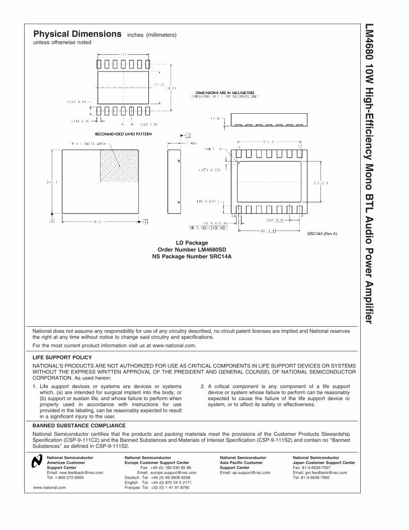
Physical Dimensions inches (millimeters)unless otherwise noted
LD PackageOrder Number LM4680SD
NS Package Number SRC14A
National does not assume any responsibility for use of any circuitry described, no circuit patent licenses are implied and National reservesthe right at any time without notice to change said circuitry and specifications.
For the most current product information visit us at www.national.com.
LIFE SUPPORT POLICY
NATIONAL’S PRODUCTS ARE NOT AUTHORIZED FOR USE AS CRITICAL COMPONENTS IN LIFE SUPPORT DEVICES OR SYSTEMSWITHOUT THE EXPRESS WRITTEN APPROVAL OF THE PRESIDENT AND GENERAL COUNSEL OF NATIONAL SEMICONDUCTORCORPORATION. As used herein:
1. Life support devices or systems are devices or systemswhich, (a) are intended for surgical implant into the body, or(b) support or sustain life, and whose failure to perform whenproperly used in accordance with instructions for useprovided in the labeling, can be reasonably expected to resultin a significant injury to the user.
2. A critical component is any component of a life supportdevice or system whose failure to perform can be reasonablyexpected to cause the failure of the life support device orsystem, or to affect its safety or effectiveness.
BANNED SUBSTANCE COMPLIANCE
National Semiconductor certifies that the products and packing materials meet the provisions of the Customer Products StewardshipSpecification (CSP-9-111C2) and the Banned Substances and Materials of Interest Specification (CSP-9-111S2) and contain no ‘‘BannedSubstances’’ as defined in CSP-9-111S2.
National SemiconductorAmericas CustomerSupport CenterEmail: [email protected]: 1-800-272-9959
National SemiconductorEurope Customer Support Center
Fax: +49 (0) 180-530 85 86Email: [email protected]
Deutsch Tel: +49 (0) 69 9508 6208English Tel: +44 (0) 870 24 0 2171Français Tel: +33 (0) 1 41 91 8790
National SemiconductorAsia Pacific CustomerSupport CenterEmail: [email protected]
National SemiconductorJapan Customer Support CenterFax: 81-3-5639-7507Email: [email protected]: 81-3-5639-7560
www.national.com
LM4680
10WH
igh-Efficiency
Mono
BTL
Audio
Pow
erA
mplifier
IMPORTANT NOTICE
Texas Instruments Incorporated and its subsidiaries (TI) reserve the right to make corrections, modifications, enhancements, improvements,and other changes to its products and services at any time and to discontinue any product or service without notice. Customers shouldobtain the latest relevant information before placing orders and should verify that such information is current and complete. All products aresold subject to TI’s terms and conditions of sale supplied at the time of order acknowledgment.
TI warrants performance of its hardware products to the specifications applicable at the time of sale in accordance with TI’s standardwarranty. Testing and other quality control techniques are used to the extent TI deems necessary to support this warranty. Except wheremandated by government requirements, testing of all parameters of each product is not necessarily performed.
TI assumes no liability for applications assistance or customer product design. Customers are responsible for their products andapplications using TI components. To minimize the risks associated with customer products and applications, customers should provideadequate design and operating safeguards.
TI does not warrant or represent that any license, either express or implied, is granted under any TI patent right, copyright, mask work right,or other TI intellectual property right relating to any combination, machine, or process in which TI products or services are used. Informationpublished by TI regarding third-party products or services does not constitute a license from TI to use such products or services or awarranty or endorsement thereof. Use of such information may require a license from a third party under the patents or other intellectualproperty of the third party, or a license from TI under the patents or other intellectual property of TI.
Reproduction of TI information in TI data books or data sheets is permissible only if reproduction is without alteration and is accompaniedby all associated warranties, conditions, limitations, and notices. Reproduction of this information with alteration is an unfair and deceptivebusiness practice. TI is not responsible or liable for such altered documentation. Information of third parties may be subject to additionalrestrictions.
Resale of TI products or services with statements different from or beyond the parameters stated by TI for that product or service voids allexpress and any implied warranties for the associated TI product or service and is an unfair and deceptive business practice. TI is notresponsible or liable for any such statements.
TI products are not authorized for use in safety-critical applications (such as life support) where a failure of the TI product would reasonablybe expected to cause severe personal injury or death, unless officers of the parties have executed an agreement specifically governingsuch use. Buyers represent that they have all necessary expertise in the safety and regulatory ramifications of their applications, andacknowledge and agree that they are solely responsible for all legal, regulatory and safety-related requirements concerning their productsand any use of TI products in such safety-critical applications, notwithstanding any applications-related information or support that may beprovided by TI. Further, Buyers must fully indemnify TI and its representatives against any damages arising out of the use of TI products insuch safety-critical applications.
TI products are neither designed nor intended for use in military/aerospace applications or environments unless the TI products arespecifically designated by TI as military-grade or "enhanced plastic." Only products designated by TI as military-grade meet militaryspecifications. Buyers acknowledge and agree that any such use of TI products which TI has not designated as military-grade is solely atthe Buyer's risk, and that they are solely responsible for compliance with all legal and regulatory requirements in connection with such use.
TI products are neither designed nor intended for use in automotive applications or environments unless the specific TI products aredesignated by TI as compliant with ISO/TS 16949 requirements. Buyers acknowledge and agree that, if they use any non-designatedproducts in automotive applications, TI will not be responsible for any failure to meet such requirements.
Following are URLs where you can obtain information on other Texas Instruments products and application solutions:
Products Applications
Audio www.ti.com/audio Communications and Telecom www.ti.com/communications
Amplifiers amplifier.ti.com Computers and Peripherals www.ti.com/computers
Data Converters dataconverter.ti.com Consumer Electronics www.ti.com/consumer-apps
DLP® Products www.dlp.com Energy and Lighting www.ti.com/energy
DSP dsp.ti.com Industrial www.ti.com/industrial
Clocks and Timers www.ti.com/clocks Medical www.ti.com/medical
Interface interface.ti.com Security www.ti.com/security
Logic logic.ti.com Space, Avionics and Defense www.ti.com/space-avionics-defense
Power Mgmt power.ti.com Transportation and Automotive www.ti.com/automotive
Microcontrollers microcontroller.ti.com Video and Imaging www.ti.com/video
RFID www.ti-rfid.com
OMAP Mobile Processors www.ti.com/omap
Wireless Connectivity www.ti.com/wirelessconnectivity
TI E2E Community Home Page e2e.ti.com
Mailing Address: Texas Instruments, Post Office Box 655303, Dallas, Texas 75265Copyright © 2011, Texas Instruments Incorporated