3-channel constant current led driver datasheet.pdf · 2016-07-21 · tls3001 3-channel costant...
TRANSCRIPT

TLS3001 3-channel costant current LED Driver
1
3-channel Constant Current LED Driver (V2.2)
TERALANE SEMICONDUCTOR INC.
ADDRESS:7th Floor,Building 3,China Academy of Science and Technology
Development,Gaoxin South Road 1, Nanshan
District,Shenzhen,P.R.china
Tel:86-755-8630 9506
Fox:86-755-8630 9523

TLS3001 3-channel costant current LED Driver
2
Features
3 constant-current output channels, constant output current invariant to load voltage change
Output current range: 0~30mA,
Output current adjusted through an external resistor. the default value is 20 mA with a 620 Ohm external resistor
Manchester communication interface
Single wire data transmission
Strong drive ability, The max TLS3001 IC in series :1024
8 bit color depth PWM control
Staggered output dalay:80ns
Low power consume:<100mW
Excellent output current accuracy:
Between channels: <±1.5%,and
Between Ics: <±3%
100KHz~1MHz clock frequency
Supply voltage range: 5~17V
ESD > 7KV
Typical application
Signel pix light (SOP14/SSOP10)
Twinkle light(SOP8apply in 5V
system)
Signboard(customized)
Product Description
TLS3001 provide Single wire data transmission and contains 3 constant-current output channels and internal Pulse Width Modulation (PWM) control with 8-bit color depth. At TLS3001 output stages, three regulated current port are designed to provide uniform and constant current sinks with a wide range of loading variations. The output current can be present through an external resistor, and the default value is 20mA. TLS3001 provides supply voltage range from 5V to 17V through internal voltage regulator. TLS3001 guarantees to endure maximum 17V at the output ports.

TLS3001 3-channel costant current LED Driver
3
Block Diagram
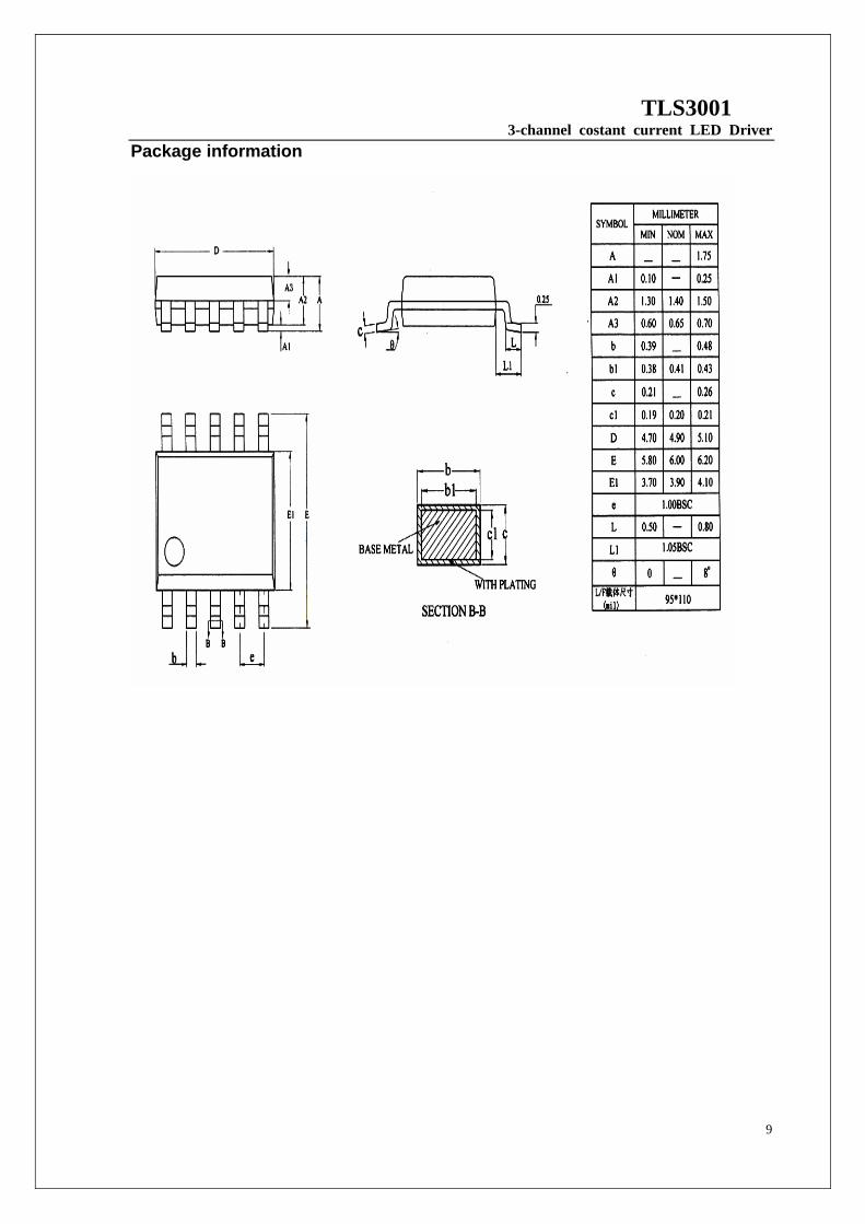
Maximum Ratings
CHARACTERISTIC SYMBOL RATING UNIT
Supply Voltage VDD 17 V
Input Voltage(SDI) VIN -0.4~Vcap+0.4 V
Output Current IOUT 30 mA
Endurance Voltage of Output VDS 17 V
GND Terminal Current IGND 95 mA
Clock Frequency FDCLK 0.1~2 MHz
SOP14 0.87
SSOP10 0.625 Endurance power PDmax
SOP8 0.625
W
Operating Temperature Topr -45 ~ +85 ℃
Storage Temperature Tstg -55 ~ +125 ℃

TLS3001 3-channel costant current LED Driver
4
Electrical Characteristics
CHRACTERISTIC SYMBOL CONDITION MIN. TYP. MAX. UNIT
Supply Voltage VDD 5 17 V
Output Current Vcap 3.1 3.15 3.32 V
Current Skew(channel)
IOUT 0 20 30 mA
Current Skew(IC) dIOUT1
Iout=20mA VR=
461 mV
R=620Ω
±
1.5 ±3 %
Current Skew vs. Supply Voltage
dIOUT2
Iout=20mA VR=
461 mV
R=620Ω
±3 ±6 %
Supply Voltage %/dVDD Supply Voltage=
5~17V
±
0.2 ±0.5 %/V
Switching Characteristics CHRACTERISTIC SYMBOL MIN. TYP. MAX. UNIT
Internal clock Frequency OSC 13 27 MHz
Pulse Width 19 38 ns
Staggered output delay 19 38 ns
Output Rise Time of Output Ports 80 ns
Output Fall Time of Output Ports 300n ns
Internal clock Frequency 600n ns
TLS3001 3-channel costant current LED Driver
5
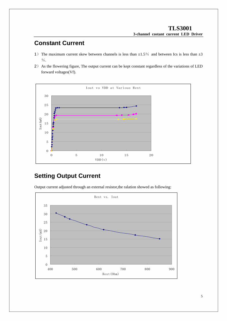
Constant Current 1) The maximum current skew between channels is less than ±1.5% and between Ics is less than ±3
%. 2) As the flowering figure, The output current can be kept constant regardless of the variations of LED
forward voltages(Vf).
Iout vs VDD at Various Rext
0
5
10
15
20
25
30
0 5 10 15 20
VDD(v)
Iout(mA)
Setting Output Current Output current adjusted through an external resistor,the ralation showed as following:
Rext vs. Iout
0
5
10
15
20
25
30
35
400 500 600 700 800 900
Rext(Ohm)
Iout(mA)
TLS3001 3-channel costant current LED Driver
6
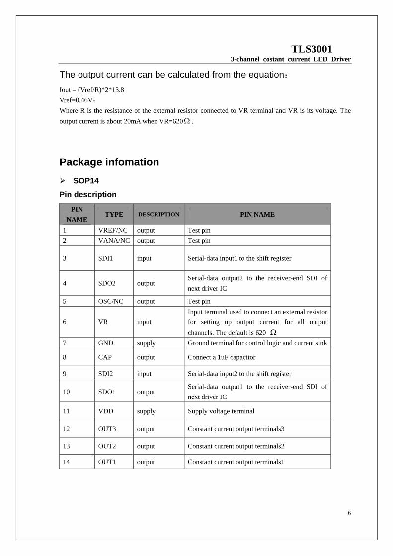
The output current can be calculated from the equation: Iout = (Vref/R)*2*13.8 Vref=0.46V; Where R is the resistance of the external resistor connected to VR terminal and VR is its voltage. The output current is about 20mA when VR=620Ω .
Package infomation SOP14
Pin description
PIN NAME
TYPE DESCRIPTION PIN NAME
1 VREF/NC output Test pin 2 VANA/NC output Test pin
3 SDI1 input Serial-data input1 to the shift register
4 SDO2 output Serial-data output2 to the receiver-end SDI of next driver IC
5 OSC/NC output Test pin
6 VR input Input terminal used to connect an external resistor for setting up output current for all output channels. The default is 620 Ω
7 GND supply Ground terminal for control logic and current sink
8 CAP output Connect a 1uF capacitor
9 SDI2 input Serial-data input2 to the shift register
10 SDO1 output Serial-data output1 to the receiver-end SDI of next driver IC
11 VDD supply Supply voltage terminal
12 OUT3 output Constant current output terminals3
13 OUT2 output Constant current output terminals2
14 OUT1 output Constant current output terminals1
Ω

TLS3001 3-channel costant current LED Driver
7
Package information
TLS3001 3-channel costant current LED Driver
8
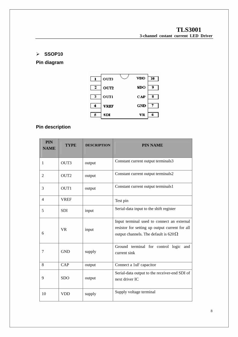
SSOP10
Pin diagram
Pin description
PIN
NAME TYPE DESCRIPTION PIN NAME
1 OUT3 output Constant current output terminals3
2 OUT2 output Constant current output terminals2
3 OUT1 output Constant current output terminals1
4 VREF Test pin
5 SDI input Serial-data input to the shift register
6 VR input
Input terminal used to connect an external resistor for setting up output current for all output channels. The default is 620Ω
7 GND supply Ground terminal for control logic and current sink
8 CAP output Connect a 1uF capacitor
9 SDO output Serial-data output to the receiver-end SDI of next driver IC
10 VDD supply Supply voltage terminal
TLS3001 3-channel costant current LED Driver
9
Package information

TLS3001 3-channel costant current LED Driver
10
SOP8 Pin diagram
Pin description
PIN NAME
TYPE DESCRIPTION PIN NAME
1 SDI input Serial-data input to the shift register
2 VR input
Input terminal used to connect an external resistor for setting up output current for all output channels. The default is 620Ω
3 GND supply Ground terminal for control logic and current sink
4 SDO output Serial-data output to the receiver-end SDI of next driver IC
5 VDD supply Supply voltage terminal
6 OUT3 output Constant current output terminals3
7 OUT2 output Constant current output terminals2
8 OUT1 output Constant current output terminals1

TLS3001 3-channel costant current LED Driver
11
Package information
TLS3001 3-channel costant current LED Driver
12
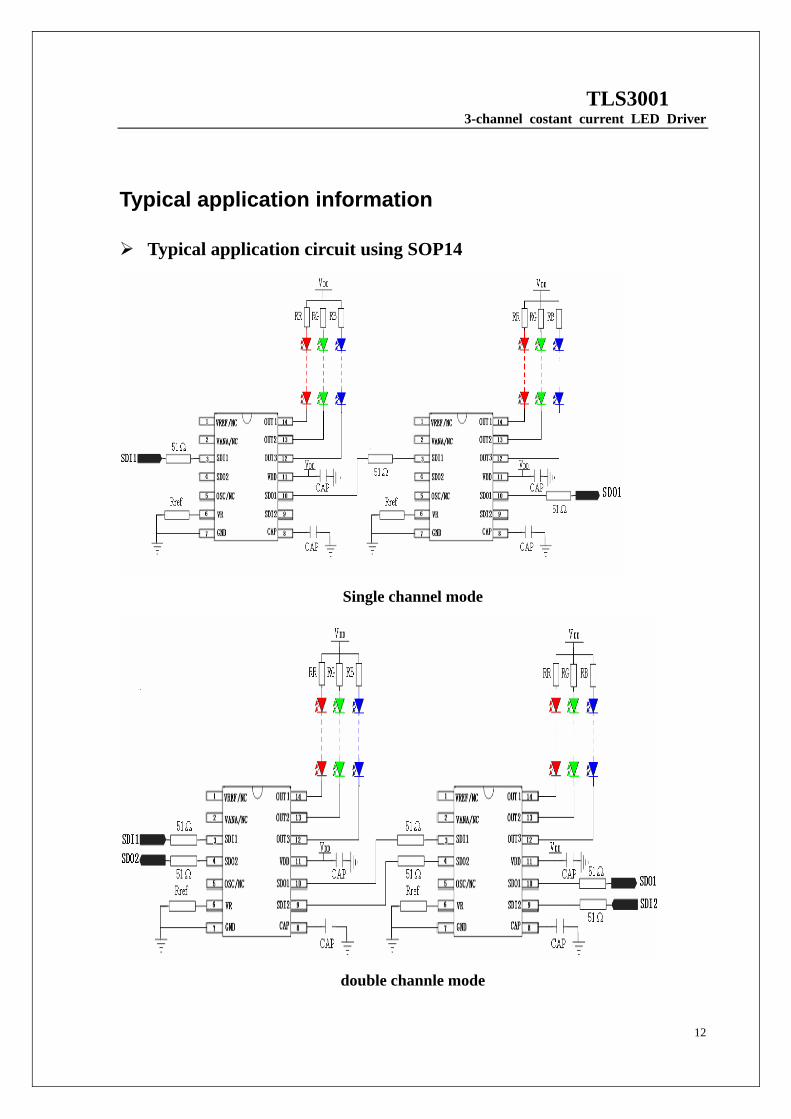
Typical application information
Typical application circuit using SOP14
Single channel mode
double channle mode

TLS3001 3-channel costant current LED Driver
13
Typical application circuit using SSOP10
Typical application circuit using SOP8
TLS3001 3-channel costant current LED Driver
14
Application notice VDD Supply voltage range
Supply voltage range using SOP14 and SSOP10:5-17V,
Supply voltage range using SOP8:4.5-7.5V
Place a 0.1uF bypass capacitor between VDD and GND terminal
In order to transmit data to more nodes, the clock frequency of input data must be between
100Khz~2MHz and the clock freqency of output data is suggested to be set below 1Mhz
The max voltage of SDI terminal must be below 3.5V
The high level voltage of SDO terminal is 3.3V
To transmit data to more node, minimize the distributed capacitor of SDO and SDO.
It is recommended to low the VDS considering the package power dissipating limits. Typically, the
output current rang is from 10mA to 40mA with VDS ranging from 0.5V to 0.8V.
Add a triode protection circuit to low the supply voltage below 17V, if the supply voltage is higher
than 17V for the LEDs in series is too much.
Unused channels must be floating or pull up when using SOP14 in single-channel mode.