-3 1966 - core.ac.uk
TRANSCRIPT

I c
I ‘ I I 1 I I I 8 I 1 I E 1 I I I I I
THIN-FIIM PERSONAL COMMUNICATIONS
1 AND !lEUmlTR.Y SYSTEM g.FPcTs)
For the period -3 of eptember 24, 1966 t o December 24, 1966
-- 2c J Contract No. M A S 9-3924 27 6
Submitted t o
National Aeronautics and Apace Administration Planned Spacecraft Center
Houston, Texas
b
https://ntrs.nasa.gov/search.jsp?R=19670009400 2020-03-16T18:53:17+00:00ZCORE Metadata, citation and similar papers at core.ac.uk
Provided by NASA Technical Reports Server
TABU OF CONTENTS
1. INTRODUC !IT ON
2. TECHNICAL DISCUSSION
2.1 RF Modulatiorl. 2.2 RF Buer Amplifier 2.3 Receiver RF 2.4 I!? AmpWier
3 . PROJECT SCHEDULE
3.1 PERT Chart 3.2 Estimate of Thin-Film Components
4. MODULE PROCESSING INFORMATION
Appendix A -0 Deposition Mask Drawings
Page
1
2
2 4 4 7
7
9 11
ll
A-1
F
LIST OF ILLUSTRATIONS
Figure
1 w 2 R F
Modulation Stages,
Power Amplifier
Oscil lator and "ripler
3 Receiver RF Amplifier
k IF Amplifier, AGC, and Audio Circuits
PERTChart
Page
3
5 6
8
10
1. INTRODUCTION
T h i s report f o r t he third quarter of Phase B is submitted i n om-
pliance with Contract NAS 9-3924 between NASA-HousCon and Melparp Inc. The
ultimate objective of the contract is to construct a thin-film personal
communication and telemetry system, During Phase B, the objective i s t o
design and qonstruct the circuit modules t ha t will be used i n Phase C to
package the t o t a l syatem. Each module i s designed t o incorporate thin-film
c i r c u i t r y t o the greatest; extent gossipls.
Progress during the past quarterr did not meet our e a r U e r expec$ations.
Three problem areas which contributed delays are:
1. Epoxy packaging of VCO's: The center frequency and range of the
VCO's changed a f t e r pottiqg,
2. Thin-film t rans is tor stakciliby and noise: Attempts t o use the
tun-f i lm Cretnsirstors have bssn d$acouragiqg ouwg t o t h e i r dc i n s t a b i l i t y
and high noise figure.
3. 300-Mc tuning procedures: It i s desirable t o use fixed capacitors
and tunable inductors i n the tkdn-film RF modules,
d i f fqcul t ies i n designing the capacitor networks i n t h i n - f i b form.
We have encowtered some
These problems will not in te r fe re with the overal l t ask objective,
but will require tha t the module delivery schedule be modified,
FERT chart is included i n this report,
A revised
The epoxy coating tha t has been used f o r an outer oovering on the
modules provtdes a r ig id package, but appareQtly induces stress on the cir-
cui t camponents,
require t ha t the bd iv idua l components remain essenltially unchanged a f t e r
I n the case of the VCO's, the c i r c u i t specifications
1
potting.
epoxy covering and del iver the modules with the wax covering only o r with an
outer coating of RTV.
I n the next attempt a t packaging the VCOfs, we w i l l eliminate the
Development work is continuing on the thin-film transis tors . We were
able to use the t rans is tors i n the source followers i n the "Summing Resistqr
Netwrk" module.
o the r module s . We will continue t o evaluate the t r ans i s to r s f o r use i n Che
The HF tuning procedure is d i f f i c u l t because the in te rs tage capacitor
networks determine both the impedance match and the frequency of operation.
The thin-film oapacitors must be deposited with close tolerance t o the d e s i p
values because trimming methods for capacitors introduce paras i t ic indvctancs
or resistance.
trimming procedure,
Further design e f for t w i l l be required t o f ind a suitable RF
2, mmcAL DISCUSSION
I n previous repor%s, we have given the schematio and c i r c u i t d e s c r i p
t i o n of the t r a n m i t t e r except for RF modulation and power output stages,
These a i r c u i t s and the receiver c i r c u i t s will be described i n t h i s report.
2.1 BF ModulaOion
A c i r cu i t diagram of the RF modulation, osc i l la tor , and 'Fripler stages
is shown i n figure 1,
quarterly report (Phase B),
0.7 V peak t o peak when loaded with the fol lowbg stage.
The osc i l l a to r and t r i g l e r w e r e described i n the first
The RF signal f r o m the t r i p l e r i s approxhate3.y
A single stsge of
gate modulation w i l l not provide the required l i n e a r i t y using insulated-gate
f ie ld-effect transistors. When a second stage is modulated i n tandem, as
2
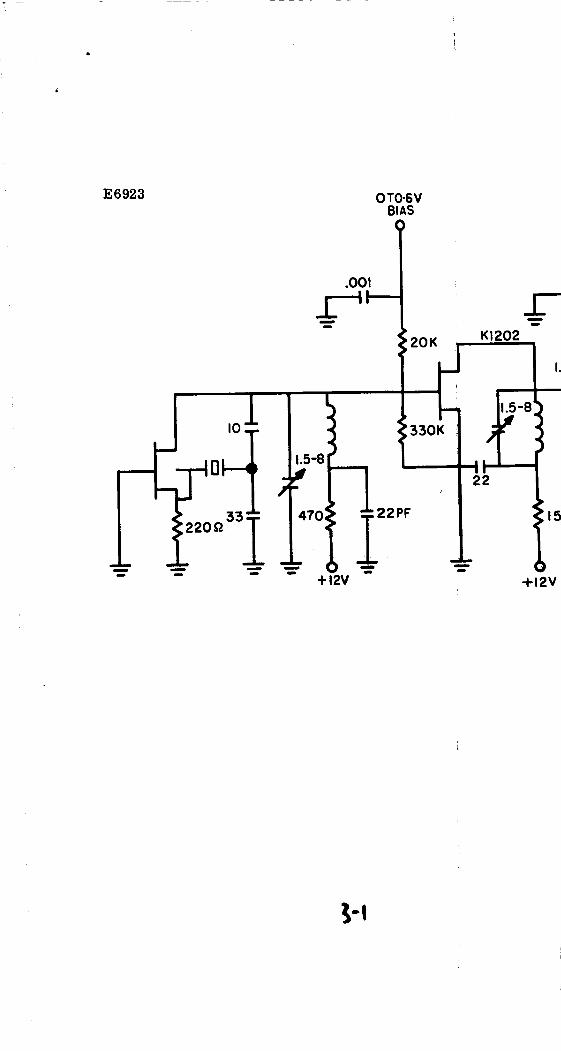
E6923 0 TO-6 V BIAS

~ MODULATION IN
Figure 1. R F Modulation 'stages, Oscillator and Tripler
TO POWER AMPLIFIER

shown i n figure 1, the modulation is l inea r t o within 4 percent and the
percent of modulation is greater than 9!$* The t rans is tor used i n these
stages i s the KMC 1201. Resistors (330 K) are placed between gate and
source t o protect the t ransis tors fram damage owing t o s t a t i c charges,
The modulation signal frm the "Filter and RF Modulator Moduleft drives
both stages identically, Fixed capacitor impedance transformatiop networks
are used between stages and tuning is accomplished with inductors.
output is an AM signal with a peak-to-peak amplitude of 8 V in to a 2 K
load, o r approximately 1 mW carr ier power, This signal i s then fed t o
the transmitter power amplifier.
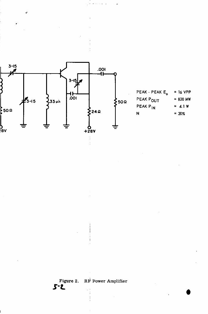
2.2 HF Power Amplifier
The
The low-power modulated signal. is fed in to a conventional t rans is tor
amplifier; i.e., g s i n d e stage of c lass A followed by two stages of c lass C.
(See f$gum 2.) The f i n a l output can be driven t o 16 V peak t o peak acrogs
50 ohms f o r a peak power of 820 mW. U t h o r without modulation the oar r ie r
power is 1 9 mW. !-
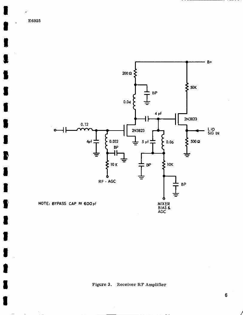
2.3 Bceiver RF
F'igw 3 shows the receiver FU? input, A 2N3823 FET i s used aq the RF
amplif$er,
t ransis tor .
An IF frequency-bypass network i s included i n the interstage coupling net
wgrk. The liF stage has B gain of 10 dB and the t o t a l voltage gain (taking
The input network patches the SO-ohm antenna t o the input of @ae
Thq second stage is a m i x e r using the same type of transistor. .z I*
f
I
i n t o account the conversion gain of the mixer) i s approximately 100. There
are two AGC points i n the receiver RE' as indicated i n figure 3. The RF AGC
detunes the input so t h a t saturation is avoided a t the maximum input signal
c levels.
4
*t
Y
E6924
C-l
I ,I
Figure 2. RP Power Amplifier
s-c
PEAK - PEAK E,
PEAK POUT
PEAK PIN
N
= 16 VPP
= 820 MW
= 4.1 W
= 20%
I 1 ' ff 1 I 8 II I
NOTE: BYPASS CAP S 6 0 0 p f MIXER BIAS 8, AGC
4 '
E6925
- 200 R
4 b 50K
E iBP - - 0.04
4 Pf 2N3823
4 1 0.06
- - 1 OK
RF - AGC ; - - BP O
B+
L io SIG IN
Figure 3. Receiver RF Amplifier
6

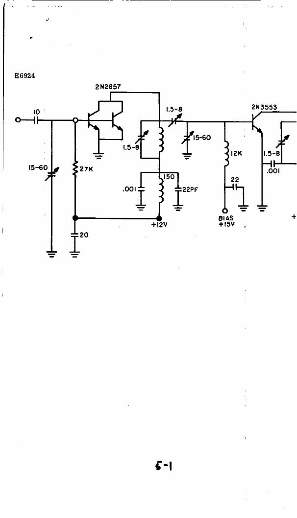
The loca l q sc i l l a to r i q essent ia l ly the same a s the oscil lator+
t r i p l e r shown i n figure 1.
2.4 IF' Amplifier 4
The I F amplifier, A N , detectors and audio amplifier are shown i n
figure 4. the first section
(Q1 through Q,) consists of four amplifier stages and is used to develop
an AGG signal f o r the RF ampllfier end mixer; the second section i s five
The IF amplifier consists of two sections:
stages with three sections of gain control.
f o r AW amplifiers ra ther than amplifying the detected s ignals with dc
amplifiers,
is designed tq be compatible with thin-film device capabili t ies.
This method uses IT stages
!he resul t ing system is not so affected by b ias changes and
Three separate detectors are used t o provide AGC. The first IF
sect ion drives two detectors, one f o r the Eli' stage and one f o r the lllixer
stage. The third AGG detector is driven from the second IF section t o
provide i ts own A N . A fourth detector is used t o provide the audio signal,
Each stage i n the I F amplifier consists of an amplifier ard a s o w e
follower, This i s necessargto prevent sapacitive loading from one stage
t o the next. A frequency selective twin-T f i l t e r is used i n the second
sect ion t o provide some degree of s e l ec t iv i ty aml noise reducC;Lon. The
output o f Q17 i s fed back t o the input of Q through &he twin-T ne+work. l4
3. PROJECT SCHEDlJU
The objective fo r this phase of tbe project i s t o del iver finisbed
modules with schematics ard specifications,
7

8 .
i 8 s 1 It Jc 3 t: II I 0 I I 8 1 I 1
8 ' E6926

0.005~ f
47af
i
l00K
1K ? *lo” 0 . 0 0 2 N f -- T %Opf
7 5 0 r E 2 y 0 .005~ f
%OPf
- P +lev
45.5H 45. H
- - I
4 AUDIO OUTPUT
‘8-& Figure 4. IF Amplifier, AGC, and Audio Circuits
The following revised list represents the complete set of modules
tha t w i l l be required f o r the transceiver along with notations on the
progress made t o date:
Module #l - Transmitter Audio Amplifier:
Module #2 - 2.3-KC Low-Pass EYlter:
Modules #3-@ - VCO's: Two modules were completed but changed
Ready f o r Delivery,
Ready fo r deposition,
character is t ics when potted. A secmd attempt a t packaging is i n process.
Modules #lo, #ll, #12 - Twin-T Notch Fi l te rs :
Modules #13 and #l4 - Diplexer &it, IMplexer Receive:
delivered.
Redesign is
required.
Module #ls - Mixer Operational AmpUfier:
Modules #16 and #l? - Xmit RF, Receiver RF:
Ready f o r packaghg.
Thin-film design i n
progress.
Modules #18-#U: - Receiver IF, AGC and Audio: Ready f o r mask fabr i -
cation.
Module #22 - Summing Resistor Network:
Modules #23, #23 - Power Supply: These modules w i l l not be f ina l ized
Ready for delivery.
u n t i l a l l okher modules are reduced t o t h i n film form. '
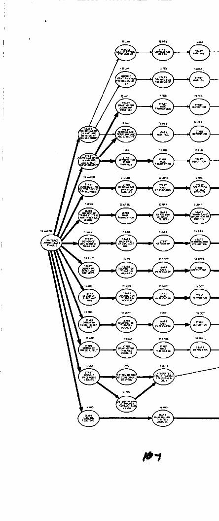
3.1 PERT Chart
A revised - PERT chart i s shown i n figure 5. The ta rge t dates f o r the
completion of modules have been changed t o r e f l ec t the present estimates.
Some of the modules w i l l not be completed during Phase B.
af fec t the overall system integration, since discrete component modules
can be used t o evaluate the finished portion of the system.
This will not
9
Y
I5 API(L I Y." I S M T
21 FE8
T R u l y c Am EVALUITION
I SEPT
DELIVERY
ISNOV
IRlY11NG A N D EVALUATION
IS Dfc
TUIYIWG AND EVALUATION
I , JAN
TRIUWNG AND EVALUATION
TRIUYNGIND EVALUATION
- .
W W W . m u . I5 APRIL 1 \ I
\ I5 APRIL
6 SEPT
f6- t .. I Figure 5. PERT Chart
10
a
1 I
3.2 Estimate of Thin-Film Components
Table I shows the pa r t count f o r the various types of components.
The current percentage figure for thin-film cmponents i s 75.
i s lower than previously reported owing t o the increased use of d i scre te
t ransis tors .
be incorporated i n the design.
T h i s figure
As improvements a r e made i n thin-film transis tors , they will
4. MODULE PROCESSING INFORMATION
Appendix A contains the deposition mask drawing for:
a.
b. Operational amplifier
e. Audio amplifier trenhnaitter
d.
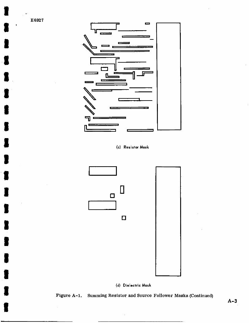
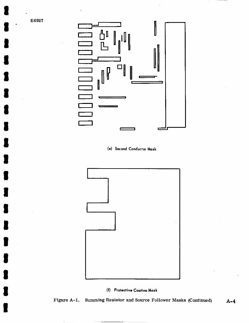
Summing resistors and source followers.
2.3-90 filter and RF modulator
5. SUMMARY AND NEXT PERIOD OBJECTIVES
Same delays have occurred i n the fabrication of thin-film modules.
Most of the modules wi l l be completed during the next quarter and system
integrat ion can begin on schedule. The RF and power supply modules will
not be reduced t o thin-- form u n t i l the first quarter of Phase 0.
Fhristing discrete component modules will be used f o r the RE' portion during:
the ea r ly par t of system integration.
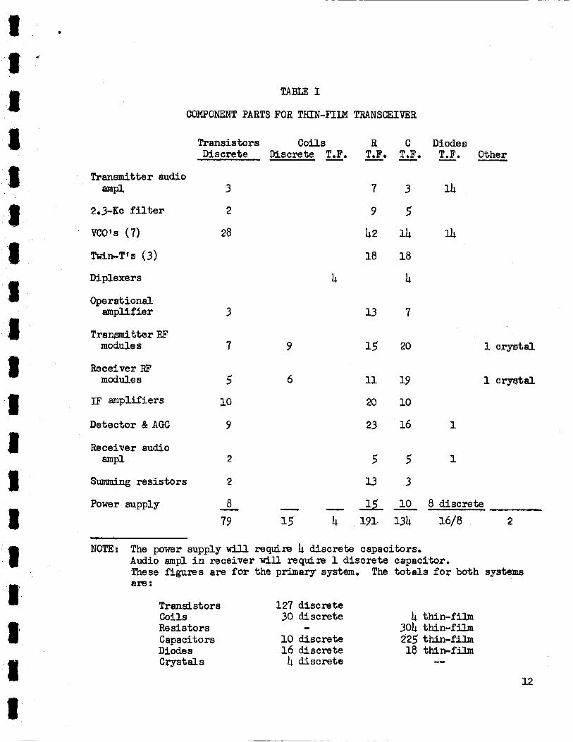
TABLE I
COMPONEXT PARTS FOR THIN-FIU
Transistors co i l s Discrete Discrete T,F.
Transmitter audSo -PI 3
2 . 3 - ~ ~ f i l t e r 2
VCO’S (7) 28
D i plexe r s 4 Operational
amplifier 3
Tranmi t te r RE’ modules 7 9
Receiver RF modules 5 6
amplifiers 10
Detector 8e AGC 9
Receiver audio 2
Summing res i s tors 2
Power supply - - - 8
79 15 4
TRANSCEIVER
R TeF - 7
9
42
18
13
15
11
20
23
5 13
C Diodes T.F. u. Other - - 3 14
5 14 4 18
4
7
20
19
10
16 1
5 1
3
1 crys t a l
1 crys ta l
15 10 8 discrete 1 9 1 134 16/8 2
NOTE: The power supply will require 4 discrete capacitors. Audio amp1 i n receiver will requim 1 discrete capacitor. These figurns are f o r the primary system, are:
The t o t a l s f o r both systems
Transistors 127 discrete Coils 30 discrete 4 t h i n - f i b Re sis tqrs - 304 thin-fikn Capacitors 10 discrete 225 thin-film
18 thin-film Diodes 16 discrete Crystal s 4 discrete _-
12

II t o 1 I s
t
APPEXDIX A
DEPOSITION MASK DRAWINGS
A-1
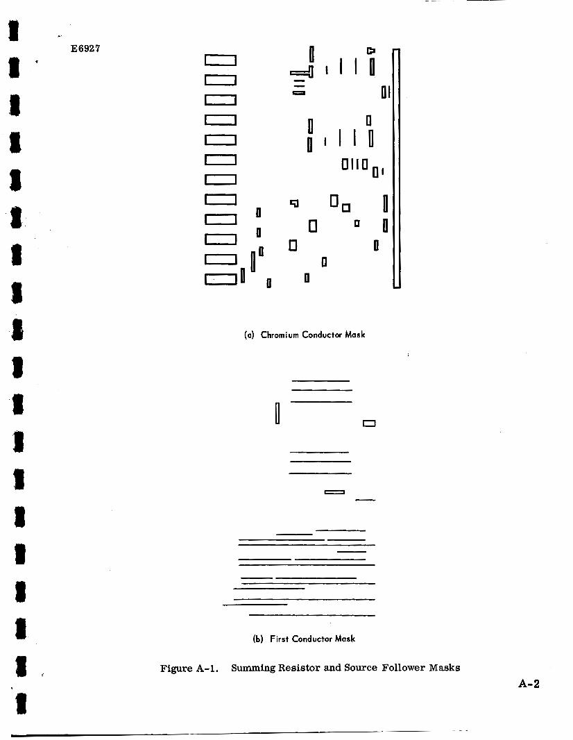
E6927 0 0 0 0 0 0
(a) Chromium Conductor Mask
(b) First Conductor Mask
Figure A-1. Summing Resistor and Source Follower Masks A-2
E6927
(c) Resistor Mask
(d) Dielectric Mask
Figure A-1. Summing Resistor and Source Follower Masks (Continued) A-3
E6927
0 0 0
.
U e I
(e) Second Conductor Mask
1
-
(9 Protective Coatina Mask
F i w e A-1. Summing Resistor and Source Follower Masks (Continued)
E6928 1 8 '
0
0
0
0
E 0
(1 0
0
(a) Chromium Conductor Mask
0 00 (b) First Gnductor Mask
Figure A-2. Operational Amplifier Masks A-5
E6928
(e) Low Value Resistors
(d) High Value Resistors
Figure A-2. Operational Amplifier Masks (Continued)
A-6
t 8 8 1 I 8
E6928
0 n o 0
0 0
;(e) Dielectric Mask
I I
- 0 -n
n - b a Y
n - 0 1 1 - 0 n
n - I&- - u *
b J P-
i .
(f) Second Conductor Mask
Figure A-2. Operational Amplifier Masks (Continued) A-7
E6928 I * 1'
(9) Protective Coating Mask
Figure A-2. Operational Amplifier Masks (Continued)
A-a

E6929 1
000000000000
0
0-
0
1 1 1 1 1 l l l 0 1 1 1 1 1 0 0 1 1 1 1 1 0
(a) .Chromium Conductor Mask
I, 0 0
0 Y
o
Figure A-3.
(b) First (Conductor Mask
Audio Amplifier and Transmitter Masks
A-9
I 1 I 1 1 8 8 I 1 8 I
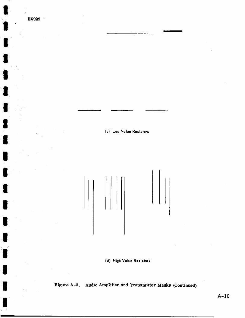
(c) Low Value Resistors
(d) High Value Resistors
Figure A-3. Audio Amplifier and Transmitter Masks (Continued)
A-10
,I I ' I 8
I 8 1 -1 I
E6929
0
8 8 1 I 8 8 8
8 a
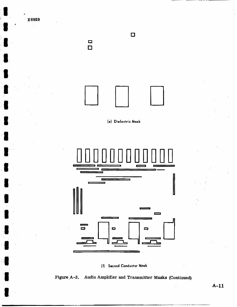
(e) Dielectric Mask
008 0
0 -- n
(4 Second Conductor Mask
Figure A-3. Audio Amplifier and Transmitter Masks (Continued)
A-11

E6929 I 3 .
8 8 I 8 I I 8
00-
(9) Protective Coating Mask!
Figure A-3. Audio Amplifier and Transmitter Masks (Continued)
A-12

I ’ E6930
I ‘ I I 8
n I 8 8 I I I I I
(a) Chromium Conductor Mask
(b) First Conductor Mask
Figure A-4. 2.3-KC Filter and RF Modulator Masks A-13
I I I I "f
(1 I I I I d 1 1 I
0
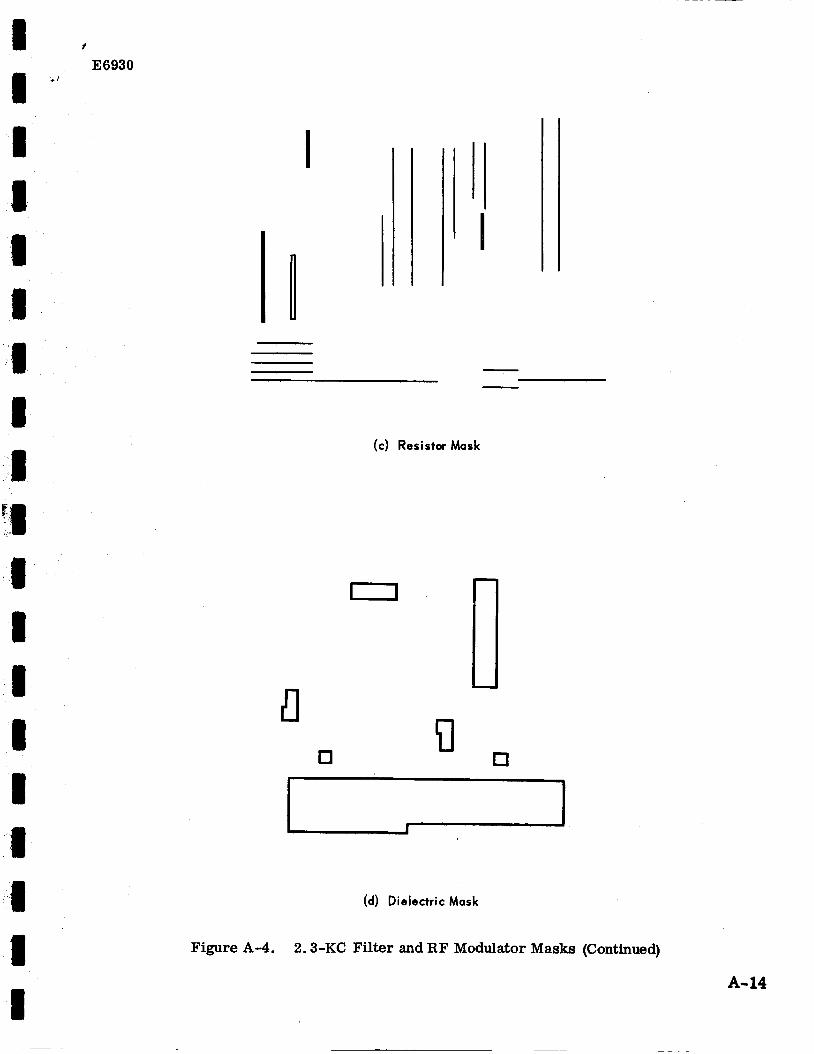
(c) Resistor Mask
0 n u
(d) Dielectric Mask
Figure A-4. 2.3-KC Filter and RF Modulator Masks (Continued)
A- 14
E6930
1
I I Y 1
1 I I I I I 1
E I
m
m
0
0
a 0 I n v 'B -0
0
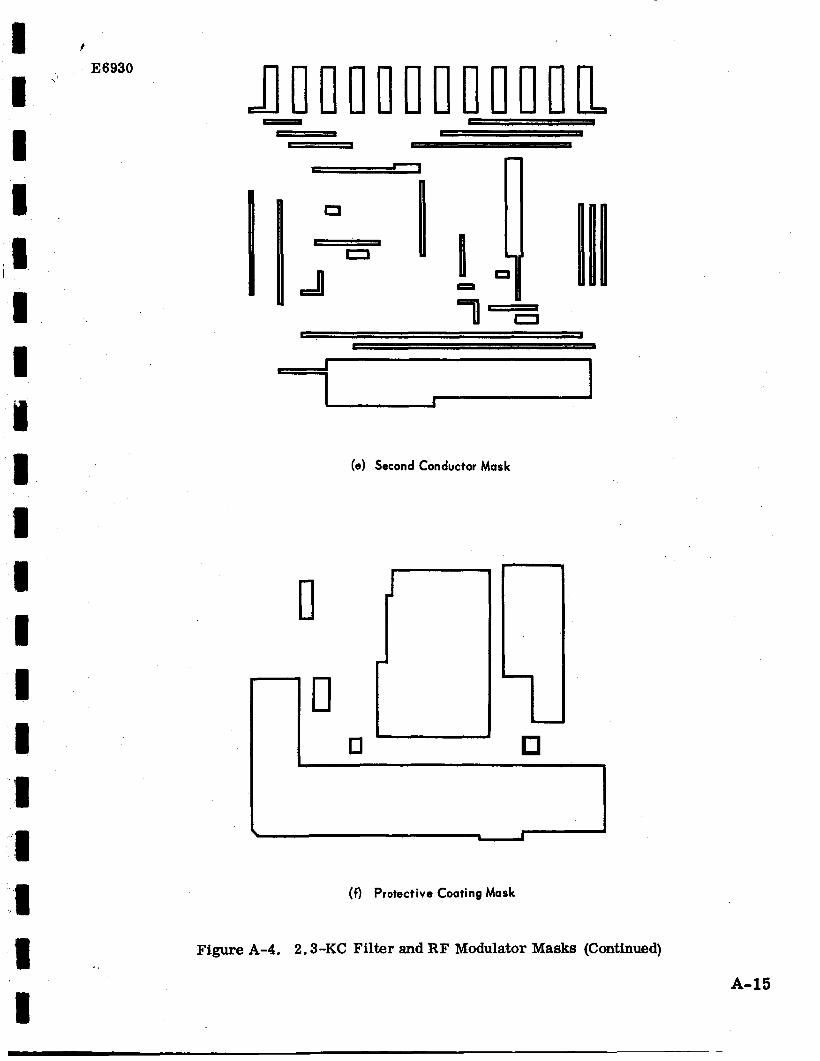
(e) Second Conductor Mask
'T I
(f) Protective Coating Mask
Figure A-4. 2.3-KC Filter and RF Modulator Masks (Continued)
A-15