2nd emc competence roup meeting - pe-region platform
TRANSCRIPT
2ND EMC COMPETENCE GROUPMEETING
Online, Thursday 11 June 2020

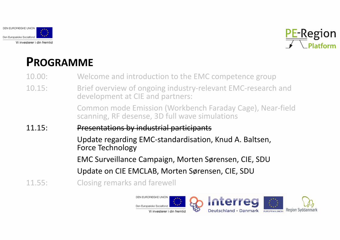
PROGRAMME10.00: Welcome and introduction to the EMC competence group10.15: Brief overview of ongoing industry‐relevant EMC‐research and
development at CIE and partners:Common mode Emission (Workbench Faraday Cage), Near‐field scanning, RF desense, 3D full wave simulations
11.15: Presentations by industrial participantsUpdate regarding EMC‐standardisation, Knud A. Baltsen, Force TechnologyEMC Surveillance Campaign, Morten Sørensen, CIE, SDUUpdate on CIE EMCLAB, Morten Sørensen, CIE, SDU
11.55: Closing remarks and farewell

MORTEN SØRENSEN• MSc in Physics, Aarhus University, PhD in electrical
engineering, Aalborg University.
• 2006‐17: Working with EMC and antennas at Bang & Olufsen a/s including initiator of‐ and 3 years as technical lead in the innovation consortium the innovation consortium "EMC ‐ First Time Right“.
• 2017‐19: Visiting Assistant Research Professor at EMCLAB Missouri University of Science & Technology and EMC research engineer at Amber Precision Instrument, San Jose
• 2019 ‐ Assoc. Professor in the field of EMC
• Research interest: System level radiated emission, near‐field scanning, ESD, EMC and simulations, ISM‐band antennas.
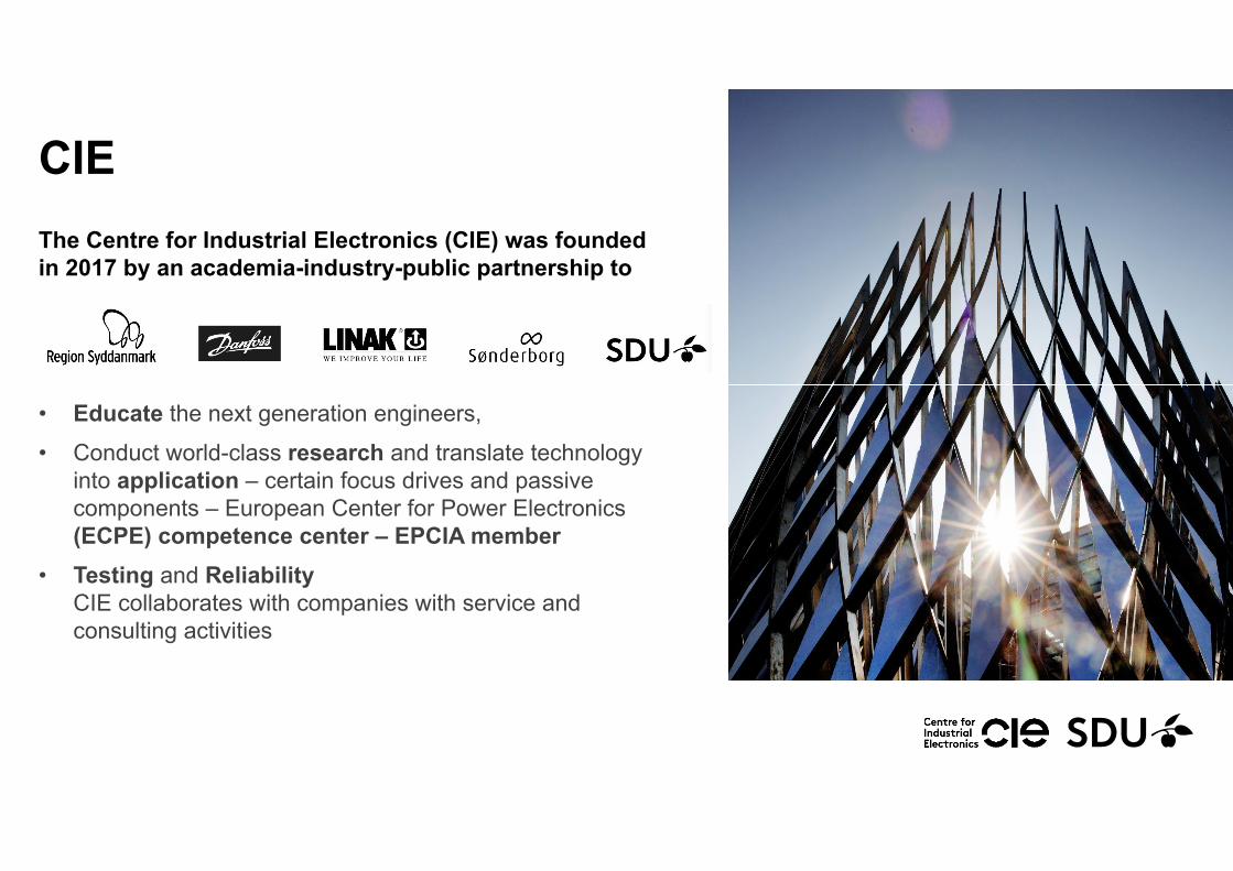
CIE The Centre for Industrial Electronics (CIE) was founded in 2017 by an academia-industry-public partnership to
• Educate the next generation engineers, • Conduct world-class research and translate technology
into application – certain focus drives and passive components – European Center for Power Electronics (ECPE) competence center – EPCIA member
• Testing and ReliabilityCIE collaborates with companies with service and consulting activities

CIE Education
Education of electronics engineers completely taught in English• Bachelor in Electronics (B.Sc., B.Eng) with focus on
industrial electronics (started in autumn 2018)• Master in Electronics (starting autumn 2020)
• Power Electronics• Embedded Software• Industrial Electronics
• Recruitment of international students• Preparation for employment in the border region• Collaboration between students and companies• Candidates: Goal is 60–70 electronic engineers per year
CIE Technology AreasCIE
Power Electronics
Active Devices
Passive devices
Topologies
EMC
Motors
Motor
Control/SW
Control
Software
Simulation
Reliability
Component level
Device Level
System level
Digitalization
Electronics
Sensing
Simulation
Communication
Protocols
Hardware
Simulation
Electrical
Thermal
Device level
System level
Applications
Renewables
Automotive
Drives
Power Distribution
Acoustics
Signal / Sound / Noise
Analysis
in place plannedpartly
in place
EMC
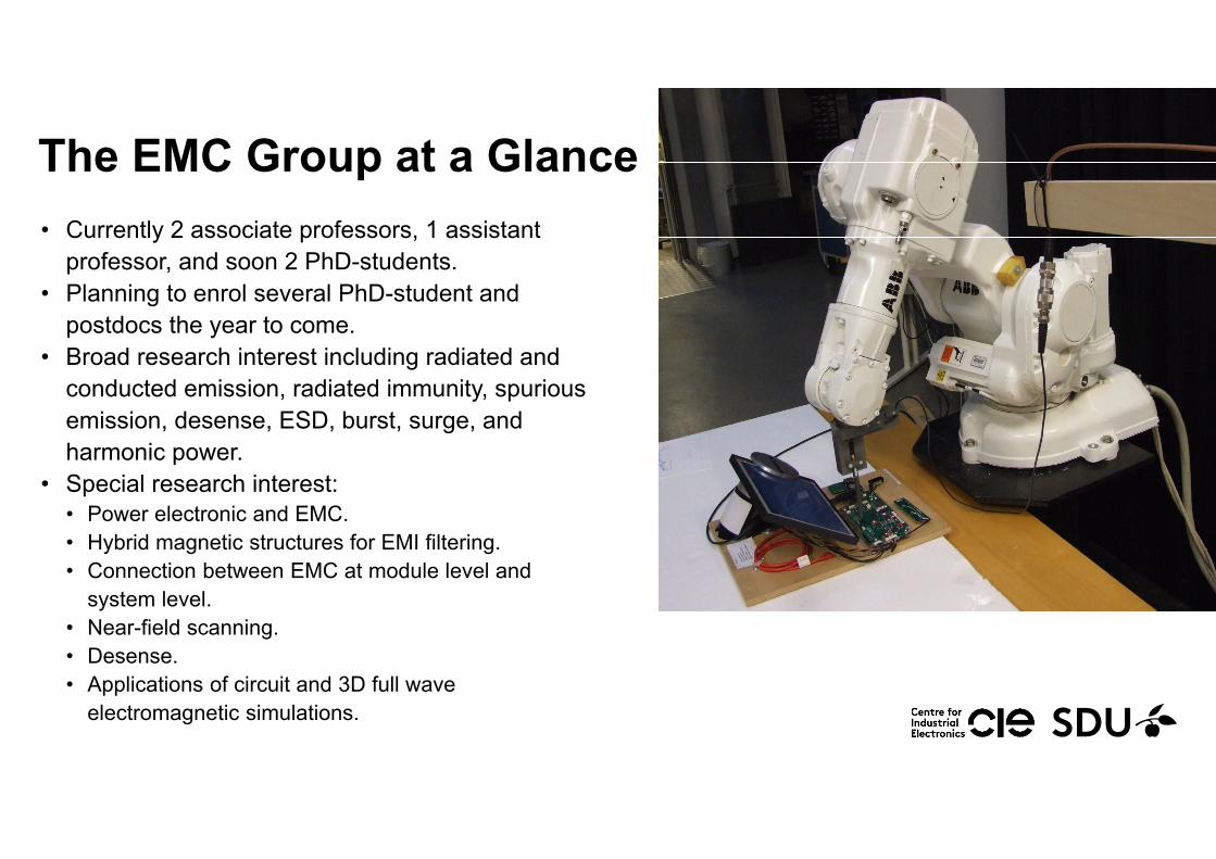
The EMC Group at a Glance• Currently 2 associate professors, 1 assistant
professor, and soon 2 PhD-students.• Planning to enrol several PhD-student and
postdocs the year to come.• Broad research interest including radiated and
conducted emission, radiated immunity, spurious emission, desense, ESD, burst, surge, and harmonic power.
• Special research interest:• Power electronic and EMC.• Hybrid magnetic structures for EMI filtering.• Connection between EMC at module level and
system level.• Near-field scanning.• Desense.• Applications of circuit and 3D full wave
electromagnetic simulations.
THE EMC COMPETENCE GROUP
PurposeThe purpose of the CIE EMC Competence Group is to share EMC related experiences between Centre for Industrial Electronics and the industry. The purpose is to increase the industry’s EMC competences and to inspire CIE to make industry relevant research – preferably with direct involvement from industry.

THE EMC COMPETENCE GROUP
Members• There is no formal membership. All engineers and researchers with interest in EMC are welcome to participate.
• Please send me an e‐mail if you want to be “member”. Members receives a Doodle for the date for next meeting.
• 37 members from more than 20 companies

THE EMC COMPETENCE GROUP
The meetings• CIE will invite for a day meeting (10‐16) with 9 months interval. The minimum agenda will be1. Recent relevant research and development within EMC (CIE)2. Share of experiences from the industry
• The time will be shared equally between item 1 and 2. The main focus is EMC but related topics are also welcome.

THE EMC COMPETENCE GROUP
The meetings• Add 1.) Faculty and students will keep the industry updated with own research and development. In addition, CIE will update the industry with trends in the international EMC Society with the on application‐oriented research with relevance for the industry.
• Add 2.) All members are given the opportunity to share problems and successes. It is an unique opportunity to get a second opinion on EMC problems and get ideas from a group of very skilled engineers. The intention is a real workshop where geeks make diagrams, drawings on the blackboard, and discuss their experiences.

PROGRAMME10.00: Welcome and introduction to the competence group10.15: Brief overview of ongoing industry‐relevant EMC‐research and
development at CIE and partners:Common mode Emission (Workbench Faraday Cage), Near‐field scanning, RF desense, 3D full wave simulations
11.15: Presentations by industrial participantsUpdate regarding EMC‐standardisation, Knud A. Baltsen, Force TechnologyEMC Surveillance Campaign, Morten Sørensen, CIE, SDUUpdate on CIE EMCLAB, Morten Sørensen, CIE, SDU
11.55: Closing remarks and farewell

OUTLINE• Pre‐Compliance test for Common Mode Emission
• Analysis and Measurement Investigation of the Workbench Faraday Cage Method, IEC 61967‐5
• Near‐field scanning and RF desense• Quick Introduction to Near‐field Scanning• Source reconstruction and RF desense• Huygens’ Box Method
• Examples of 3D Full Wave Simulations in Product Development• There is too much for one hour, the idea is just to give you an idea of the research going on. All details will not be explained.
• I will be happy to elaborate on the topics later on.

BACKGROUND• If an apparatus fails three weeks before production, it causes last minute and costly EMC rescue operations and even worse: Delay of product launch.
• In order to avoid those rescue operations, designers tend to overdesign which adds extra unnecessary cost to the final product.
14

RULE OF THUMB FOR CONDUCTED VS. DIRECT EMISSION
• Transition zone starts when the PCB exceeds ~1/10 wavelength
• Transition zone ends when the PCB exceeds ~1/2 wavelength
15
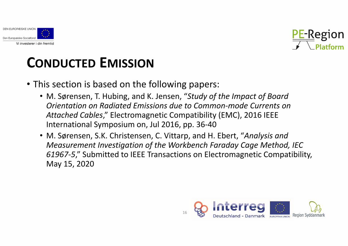
CONDUCTED EMISSION• This section is based on the following papers:
• M. Sørensen, T. Hubing, and K. Jensen, “Study of the Impact of Board Orientation on Radiated Emissions due to Common‐mode Currents on Attached Cables,” Electromagnetic Compatibility (EMC), 2016 IEEE International Symposium on, Jul 2016, pp. 36‐40
• M. Sørensen, S.K. Christensen, C. Vittarp, and H. Ebert, “Analysis and Measurement Investigation of the Workbench Faraday Cage Method, IEC 61967‐5,” Submitted to IEEE Transactions on Electromagnetic Compatibility, May 15, 2020
16

COMMONMODE EMISSION COUPLING MECHANISMS
• There are four main mechanisms by which intentional signals induce or transfer to common‐mode current on attached cables:
• Current driven (magnetic field coupling)• Voltage driven (electric field coupling)• Direct signal to I/O coupling• Finite transfer impedance in cables and connectors
17
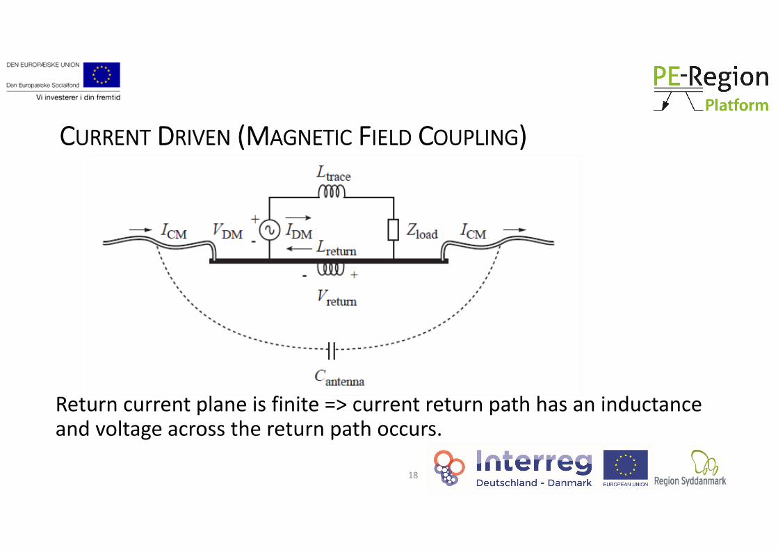
CURRENT DRIVEN (MAGNETIC FIELD COUPLING)
Return current plane is finite => current return path has an inductance and voltage across the return path occurs.
18

VOLTAGE DRIVEN (ELECTRIC FIELD COUPLING)
• The voltage across the signal generator (VDM) drives the trace relative to the return plane with cables.
19
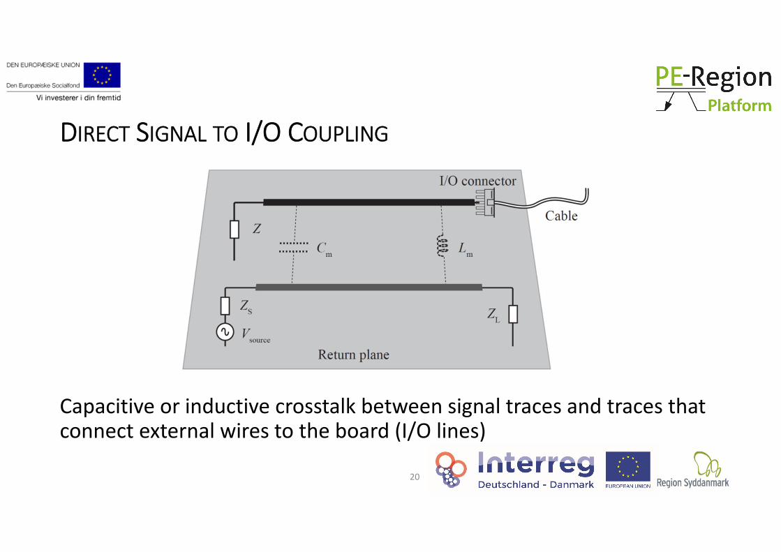
DIRECT SIGNAL TO I/O COUPLING
Capacitive or inductive crosstalk between signal traces and traces that connect external wires to the board (I/O lines)
20

IDENTIFYING VOLTAGE AND CURRENT DRIVEN SOURCES
Original
Voltage driven
Current driven
21

REFINEMENT OF THE METHOD FOR LONG TRACES
• Divide the trace into a number of electrical short subtraces.• The excitation of the ports is time shifted with the time it takes the signal to propagate from one generator to the next generator:
• time shift, δ =
• ZL = ∞ (voltage driven).• ZL = 0 (current driven).
22

STUDY OF CABLE ORIENTATION• Several models for predicting maximum radiating emission from cables attached to PCB’s have been developed.
• The predictions are based on trace length, board thickness, source location etc. ‐ but not on cable geometry.
• 150 x 225 mm PCB with three 50 Ω traces. Only one trace (120 mm long) was excited and terminated.
• One or two 1 m long cables were attached to the ground plane of the PCB.
• The cables were terminated to an infinite ground plane representing the floor of a chamber.
• Top: The traces are facing up relative to the cables and the floor of the chamber. Bottom: The traces are facing down relative to the cables and the floor of the chamber.
Traces Up
Traces Down
23

STUDY OF CABLE ORIENTATION
• The setup was simulated in CST Microwave Studio with far‐field monitors for every 10 MHz and additional far‐field monitors for every 1 MHz around cable resonances.
• Maximum radiated emission in 3 m distance was found (similar to standard radiated emission test).
• The setup was also measured in a 3 m semi‐anechoic chambers by help of a comb generator with fundamental frequency of 1 MHz.
24

EFFECT OF TRACE ORIENTATION
Traces up
Traces up
Traces down
Traces down
Traces down
Traces down
Traces downTraces down
Traces up = traces down
25
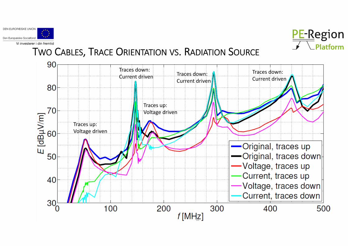
TWO CABLES, TRACE ORIENTATION VS. RADIATION SOURCE
Traces up:Voltage driven
Traces up:Voltage driven
Traces down:Current driven Traces down:
Current drivenTraces down:Current driven
26

SIMULATIONS VS. MEASUREMENTS – TWO CABLES
Voltage driven
Voltage driven
Current driven Current driven
Current driven
Voltage driven
27

WORKBENCH FARADAY CAGE (WBFC) METHOD• IEC 61967‐5. IEC Standard since 2003.• Until now there has only been a few scientific publications with theoretical‐ or measurement validation of the method.
• The WBFC method assumes that the supply and signal cable(s) are attached to an electrically small PCB. Hence, attached cables are the dominant antennas
• The method suggests that the maximum common mode emission can be estimated by loading the test points with 150 Ω resistance.
• 150 Ω is a representation for the radiation resistance of long cables and comes from empirical data.
• The PCB is placed in a small Faraday cage in order to limit the influence of the ambient noise on the test results, and in order to have defined coupling parameters to the PCB surroundings.
28
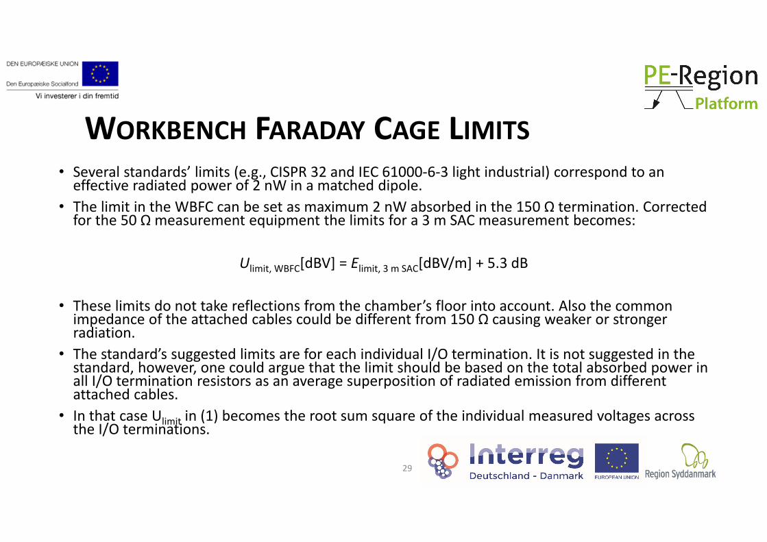
WORKBENCH FARADAY CAGE LIMITS• Several standards’ limits (e.g., CISPR 32 and IEC 61000‐6‐3 light industrial) correspond to an effective radiated power of 2 nW in a matched dipole.
• The limit in the WBFC can be set as maximum 2 nW absorbed in the 150 Ω termination. Corrected for the 50 Ωmeasurement equipment the limits for a 3 m SAC measurement becomes:
Ulimit, WBFC[dBV] = Elimit, 3 m SAC[dBV/m] + 5.3 dB
• These limits do not take reflections from the chamber’s floor into account. Also the common impedance of the attached cables could be different from 150 Ω causing weaker or stronger radiation.
• The standard’s suggested limits are for each individual I/O termination. It is not suggested in the standard, however, one could argue that the limit should be based on the total absorbed power in all I/O termination resistors as an average superposition of radiated emission from different attached cables.
• In that case Ulimit in (1) becomes the root sum square of the individual measured voltages across the I/O terminations.
29

ANALYSIS AND MEASUREMENT INVESTIGATION OF THE WBFC METHOD
• The method was analyzed by simulations and a three typical PCBs were tested by help of the method.
• The reference microstrip PCB was used in the simulations. A version with I/O coupling was also tested.
• Two 1 m long cables were attached to the PCB and terminated to ground with 0 and 150 Ω.
30

MEASUREMENT SETUP• Three typical PCBs with different IC’s (microprocessors, RAM, Ethernet communication etc.) was measured according to the WBFC method and compared with a 3 m SAC measurement. Ferrite beads were used as CMAD.
• PCM5.1, Microprocessor and Power Supply Module (DEIF)• GPM5.1, Voltage and Current Measurement Module (DEIF)• PB50, Power Supply Unit (Bang & Olufsen)
31

RESULT OF SIMULATIONS• All test cases have same trend.• Poor to fair agreement at lower frequencies. As frequencies increases, the WBFC method underestimates the radiated emission.
32
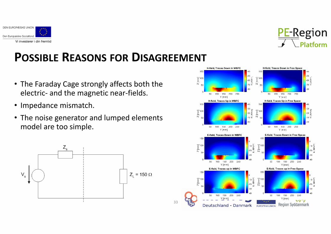
POSSIBLE REASONS FOR DISAGREEMENT
• The Faraday Cage strongly affects both the electric‐ and the magnetic near‐fields.
• Impedance mismatch.• The noise generator and lumped elements model are too simple.
33
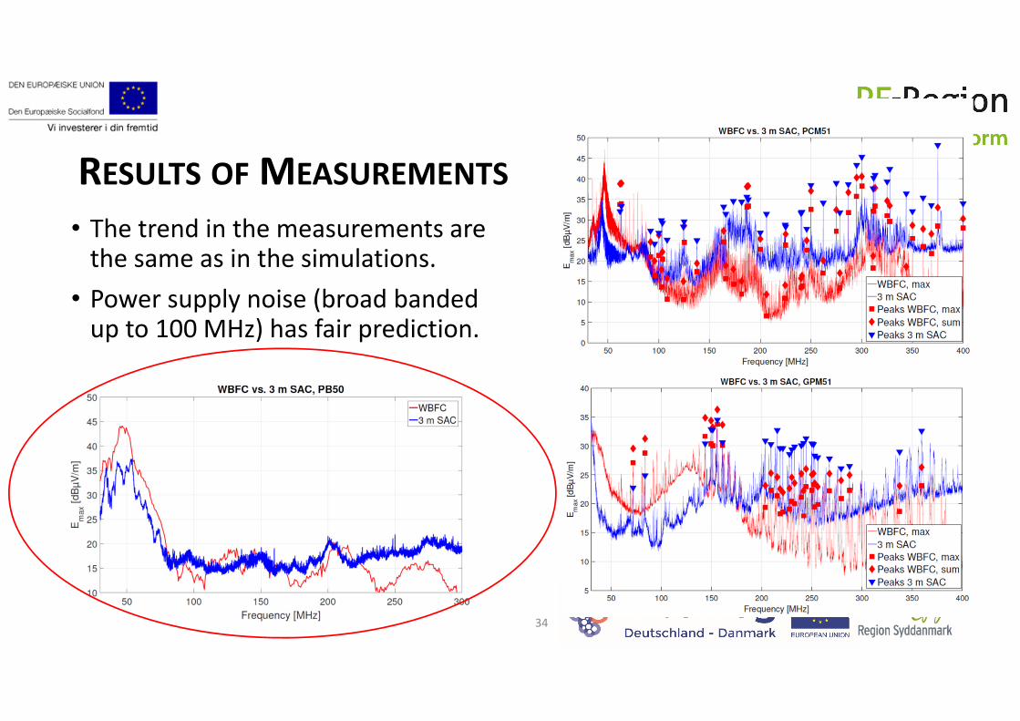
RESULTS OF MEASUREMENTS• The trend in the measurements are the same as in the simulations.
• Power supply noise (broad banded up to 100 MHz) has fair prediction.
34
CONCLUSION ON CONDUCTED EMISSION• It is possible to identify radiation sources (voltage vs. current driven) for long traces by dividing the traces into electrical short traces.
• By help of this method it was shown that maximum radiated emission differed up to 10 dB depending on the orientation of the traces. No simplified noise generator / lumped element models do predict this difference.
• IEC‐ 61967‐5, the Workbench Faraday Cage Method, does not work as intended. There is poor agreement between WBFC predictions and actually 3 m SAC measurements. The Faraday Cage itself affects the measurements.
• The WBFC has perhaps potential for switching noise. Potential student project. SMP? Inverters? Anyone?
35

OUTLINE
• Pre‐Compliance test for Common Mode Emission• Analysis and Measurement Investigation of the Workbench Faraday Cage Method, IEC 61967‐5
• Near‐field scanning and RF desense• Quick Introduction to Near‐field Scanning• Source reconstruction and RF desense• Huygens’ Box Method
• Examples of 3D Full Wave Simulations in Product Development

HOMEMADE EMC NEAR-FIELD SCANNER
Probe moves around and measure the signal on PCB
Reference probe for measuring the phase

DIFFERENT APPROACHES TO PHASE MEASUREMENTS
• Vector network analyzer in tuned receiver mode
• Phase coherent receivers
• Time domain measurement with High‐speed oscilloscopes
38

MEASUREMENT VALIDATION OF HOMEMADE NEAR‐FIELD SCANNER
39
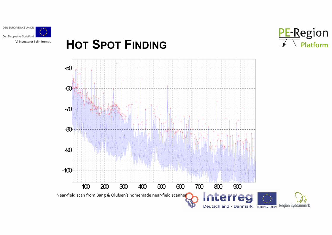
HOT SPOT FINDING
100 200 300 400 500 600 700 800 900
-100
-90
-80
-70
-60
-50
Near‐field scan from Bang & Olufsen’s homemade near‐field scanner

INTERFERENCE PROBLEM
• This IC with a clock frequency of 612.5 MHz did not interfere with the IC on right hand side.
• This IC with a clock frequency of 652.4 MHz did interfere with the IC on left hand side.
Near‐field scan from Bang & Olufsen’s homemade near‐field scanner
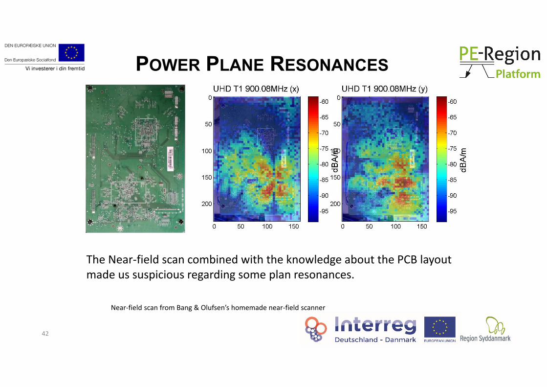
POWER PLANE RESONANCES
42
Near‐field scan from Bang & Olufsen’s homemade near‐field scanner
The Near‐field scan combined with the knowledge about the PCB layout made us suspicious regarding some plan resonances.
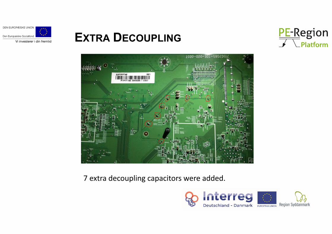
EXTRA DECOUPLING
7 extra decoupling capacitors were added.

EMISSION WAS SIGNIFICANTLY REDUCED
• Near‐field was significantly reduced.
• The current spread was reduced.
• Significant reduction in radiated emission.

RF DESENSE AND NEAR‐FIELD SCANNING• This section is a short resume of the following papers:• H. Rezaei, J. Meiguni, M. Sørensen, R. Jobava, V. Khilkevich, J. Fan, D.G. Beetner, D. Pommerenke, Source Reconstruction in Near Field Scanning using Inverse MoM for RFI Application, Accepted for future Publication in IEEE Transactions on Electromagnetic Compatibility
• M. Sørensen, I. B. Bonev, O. Franek and G. F. Pedersen, "Assessment of the Huygens’ Box Method With Different Sources Near Obstacles," in IEEE Transactions on Electromagnetic Compatibility, vol. 62, no. 2, pp. 433‐442, April 2020
• L. Li et al., "Measurement validation for radio‐frequency interferenceestimation by reciprocity theorem," 2015 IEEE International Symposium on Electromagnetic Compatibility (EMC), Dresden,
45

RF DESENSE• RF desense is a critical design challenge faced by engineers creating wireless products. Due to miniaturization, faster digital signals, multiple wireless systems and radios operating simultaneously within a small footprint, the sensitivity of receivers is compromised significantly.
• Near‐field scanning is one of the tools within electromagnetic interference.
• With the emerge of IOT it has become a hot topic within the EMC research.

PROBLEM DESCRIPTION
47
A typical desense problem: Intra-system RFI decrease the sensitivity of the antenna.
University/Center ConfidentialCEMC IAB MeetingMay 1-3, 2018
Antenna
Noise
Desired signal

FORMULATION OF THE WHOLE PROBLEMStep1: Reconstruct dipole momentsusing near field, @ Rx frequency
Step2: Use the equivalent dipole moments to estimate RFI
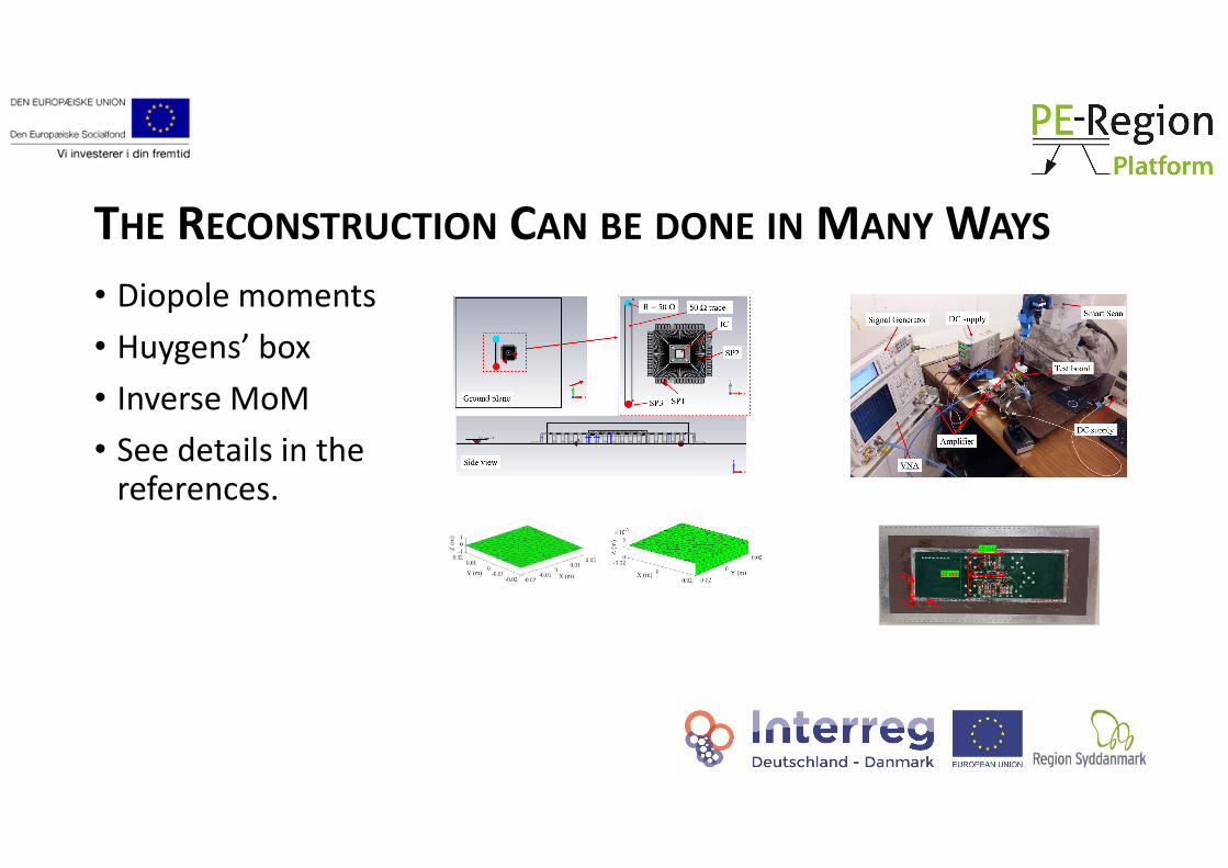
THE RECONSTRUCTION CAN BE DONE IN MANY WAYS
• Diopole moments• Huygens’ box• Inverse MoM• See details in the references.

THE OBJECTIVE OF THE HUYGENS’ BOX METHOD
• The ambitious goal is to use measured near‐field scan as source for simulations.
50

THE OBJECTIVE OF THE HUYGENS’ BOX METHOD
• Simple near‐field to far‐field is off course of interest.
• However, it is of more interest to predict the effect of obstacles by simulations.
• If a module is measured in a 3 m SAC alone as pre‐compliance test, it can be several dB of compared to the module in the final product.
0 200 400 600 800 1000-20
0
20
40
60
80
100Maximum Radiated Emission for PCB in enclosure 1
f [MHz]E
field
[dB V
/m]
Free spaceInside enclosure with connectionsResonancesInside enclosure without connectionsResonances
51
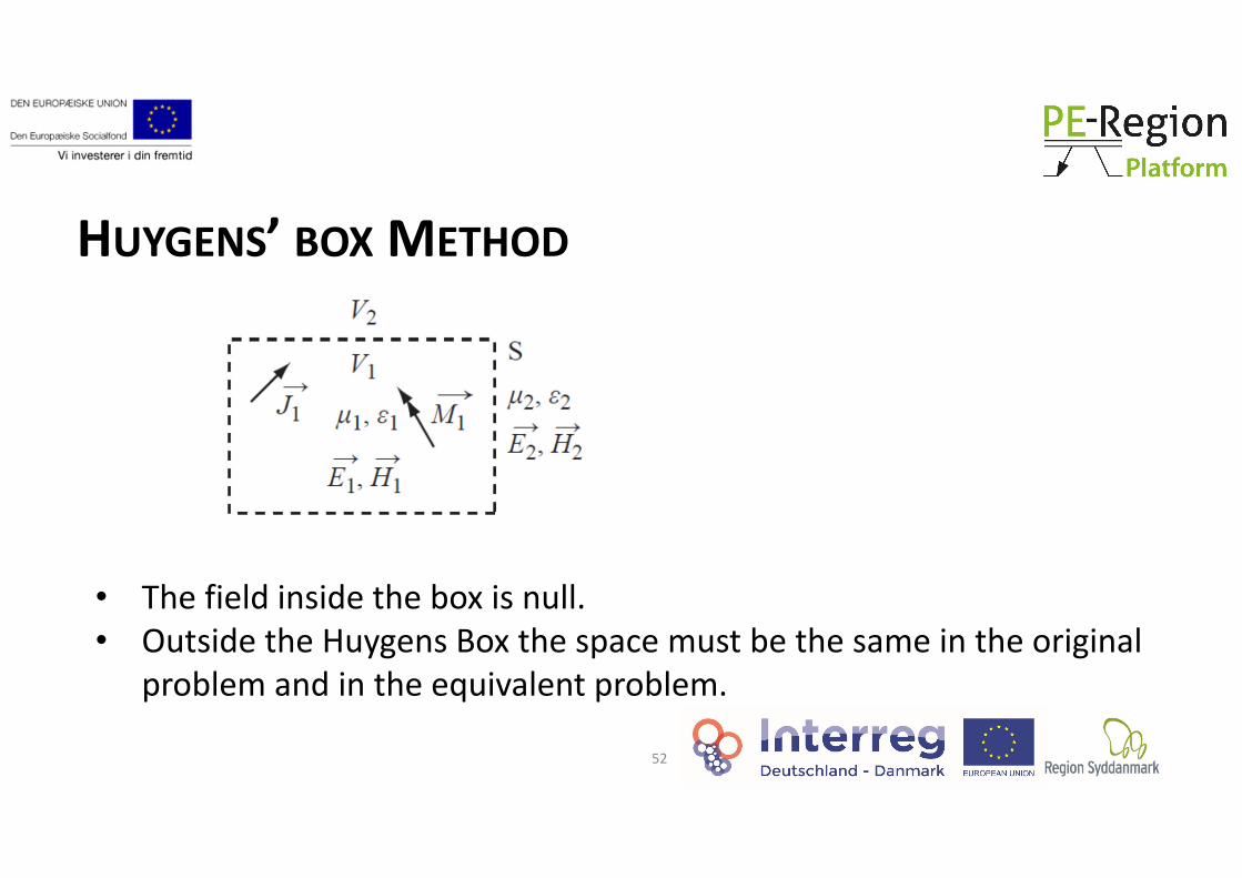
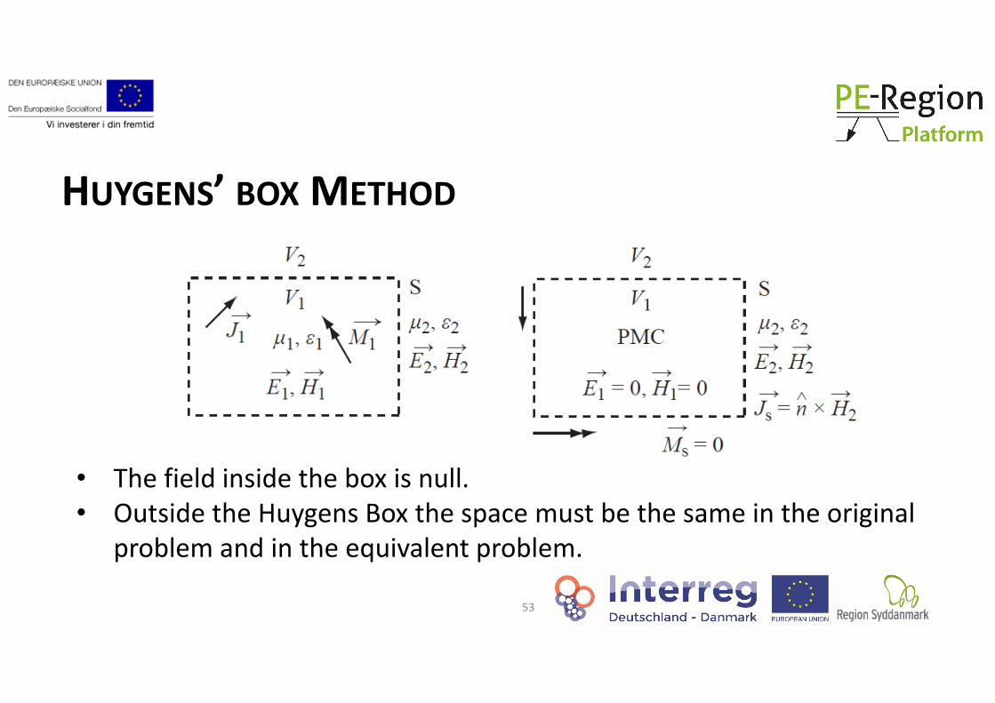
HUYGENS’ BOX METHOD
• The field inside the box is null.• Outside the Huygens Box the space must be the same in the original
problem and in the equivalent problem.
52
53
• The field inside the box is null.• Outside the Huygens Box the space must be the same in the original
problem and in the equivalent problem.
HUYGENS’ BOX METHOD
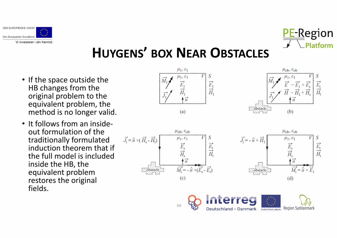
HUYGENS’ BOX NEAR OBSTACLES
• If the space outside the HB changes from the original problem to the equivalent problem, the method is no longer valid.
• It follows from an inside‐out formulation of the traditionally formulated induction theorem that if the full model is included inside the HB, the equivalent problem restores the original fields.
54
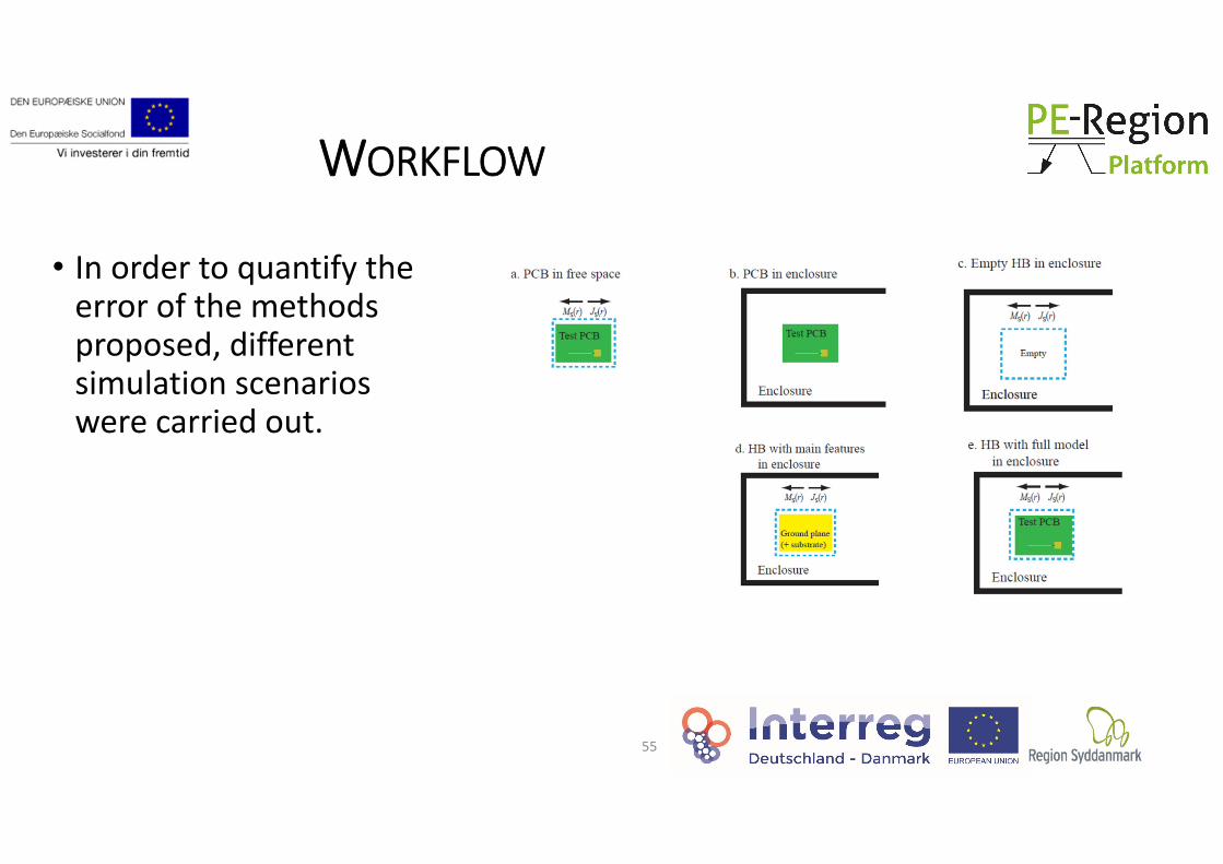
WORKFLOW
• In order to quantify the error of the methods proposed, different simulation scenarios were carried out.
55

ERROR MEASURE
0 100 200 300 400 500 600 700 800 900 100010
20
30
40
50
60
E max
[dBµ
V/m
]
0 100 200 300 400 500 600 700 800 900 1000-1
0
1
2
3
4
Peak
incr
ease
[dB]
F [MHz]
Illustration of peak increase
Peak increaseHuygens' boxReference
Far-field error 20 · log10’
56

SEVERAL COMBINATIONS OF SOURCES AND OBSTACLES
57
0 200 400 600 800 1000-20
0
20
40
60
80
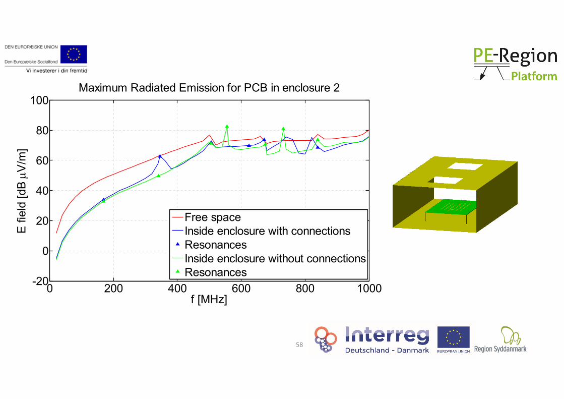
100Maximum Radiated Emission for PCB in enclosure 2
f [MHz]
E fie
ld [d
B V
/m]
Free spaceInside enclosure with connectionsResonancesInside enclosure without connectionsResonances
58

0 200 400 600 800 1000-15
-10
-5
0
5
f [MHz]
peak
incr
ease
[dB]
Peak increase for HB in enclosure 2
HB emptyResonancesHB with GNDResonancesHB with GND and substrateResonances
59
0 200 400 600 800 1000-15
-10
-5
0
5
10
15
f [MHz]
peak
incr
ease
[dB]
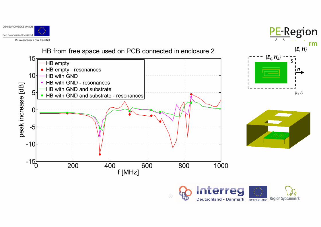
HB from free space used on PCB connected in enclosure 2
HB emptyHB empty - resonancesHB with GNDHB with GND - resonancesHB with GND and substrateHB with GND and substrate - resonances
60

0 200 400 600 800 1000-10
-5
0
5
f [MHz]
peak
incr
ease
[dB]
HB from PCB connected to ground used on PCB connected in enclosure 2
HB emptyHB empty - resonancesHB with GNDHB with GND - resonancesHB with GND and substrateHB with GND and substrate - resonances
61

CONCLUSION ON HUYGENS’ BOX METHOD
• If ground plane and substrate are included in the Huygens’ box, the method can in many cases predict up to 30 dB change caused by a nearby obstacle
• However, if there is a strong resonance or strong coupling between PCB and obstacle, the method fails – even with ground plane and substrate included.
• This was the proof of concept. Next step is to use it in practice.
62

OUTLINE
• Pre‐Compliance test for Common Mode Emission• Analysis and Measurement Investigation of the Workbench Faraday Cage Method, IEC 61967‐5
• Near‐field scanning and RF desense• Quick Introduction to Near‐field Scanning• Source reconstruction and RF desense• Huygens’ Box Method
• Examples of 3D Full Wave Simulations in Product Development

SIMULATIONS OF CABLE HARNESS• Project with Banke, Sønderborg under Clean, Industriel ElektronikInnovation (IEI)
• Traction Motor and large battery back• Objective: EMC architecture and pre‐compliance test early in project• Thanks to the Banke team for the support
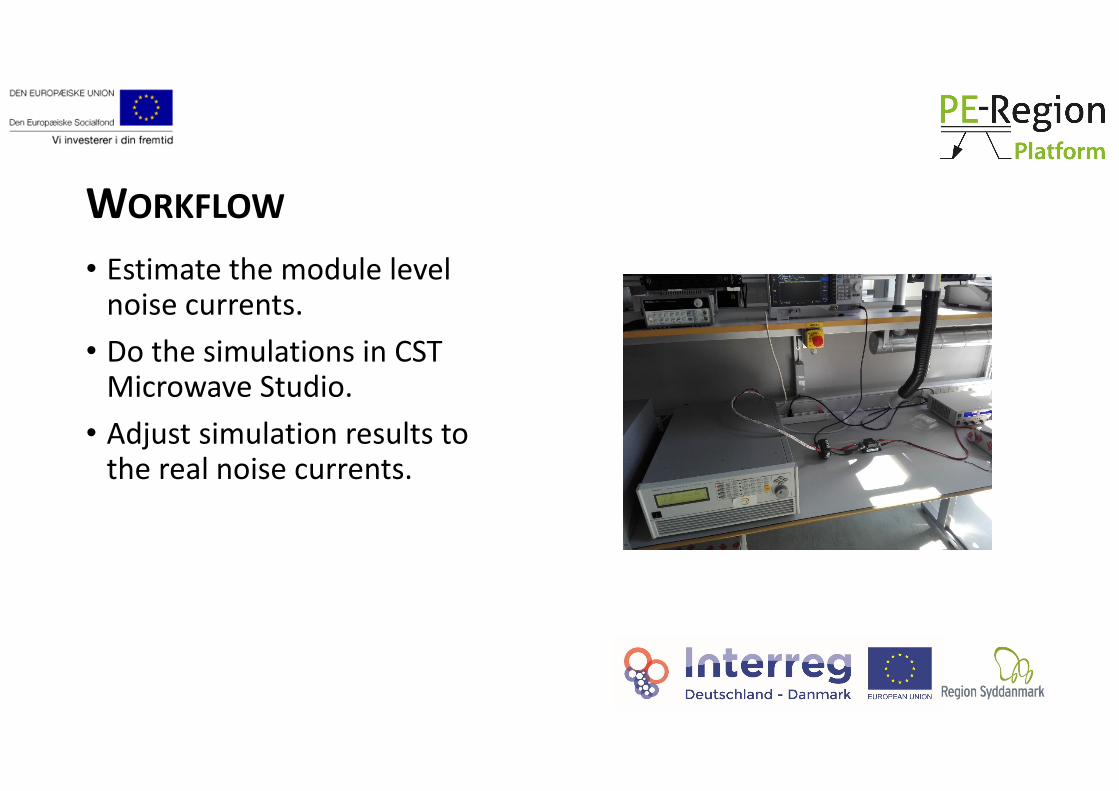
WORKFLOW
• Estimate the module level noise currents.
• Do the simulations in CST Microwave Studio.
• Adjust simulation results to the real noise currents.

COMMON MODE CURRENT DC/DC CONVERTER
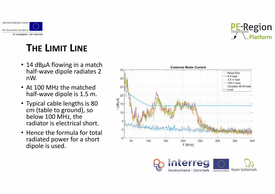
THE LIMIT LINE• 14 dBµA flowing in a match half‐wave dipole radiates 2 nW.
• At 100 MHz the matched half‐wave dipole is 1.5 m.
• Typical cable lengths is 80 cm (table to ground), so below 100 MHz, the radiator is electrical short.
• Hence the formula for total radiated power for a short dipole is used.

TRACTION MOTOR AND BATTERY PACK

Simplifying the Model
Excitation of Common Mode Current

Study Where the Current is Flowing
Input power is normalized to 0.5 W through the frequency spectrum

Radiated Emission in 3 m Distance
• Normalized to 0.5 W input power at all frequencies.
• Next step is to adjust for reel noise currents.
• The combination of simulation and measurement can early in the project give you a green, yellow or red flag.
• Base on the work a new DC/DC is sourced.


IDENTIFYING HARMFULL LOOPS

3D Full Wave Simulations
EDA files are imported to CST.Radiated Emission can be simulated.

ComparisonIn the simulation the input power is 0.5 W all over the frequency span.
As a postprocessing step the input power can be adjusted to the reel noise voltages.
PROGRAMME10.00: Welcome and introduction to the EMC competence group10.15: Brief overview of ongoing industry‐relevant EMC‐research and
development at CIE and partners:Common mode Emission (Workbench Faraday Cage), Near‐field scanning, RF desense, 3D full wave simulations
11.15: Presentations by industrial participantsUpdate regarding EMC‐standardisation, Knud A. Baltsen, Force TechnologyEMC Surveillance Campaign, Morten Sørensen, CIE, SDUUpdate on CIE EMCLAB, Morten Sørensen, CIE, SDU
11.55: Closing remarks and farewell


INDUCTION COOKING APPLIANCES• Harmonics• Conducted and Radiated Emission

LED FLOODLIGHTS
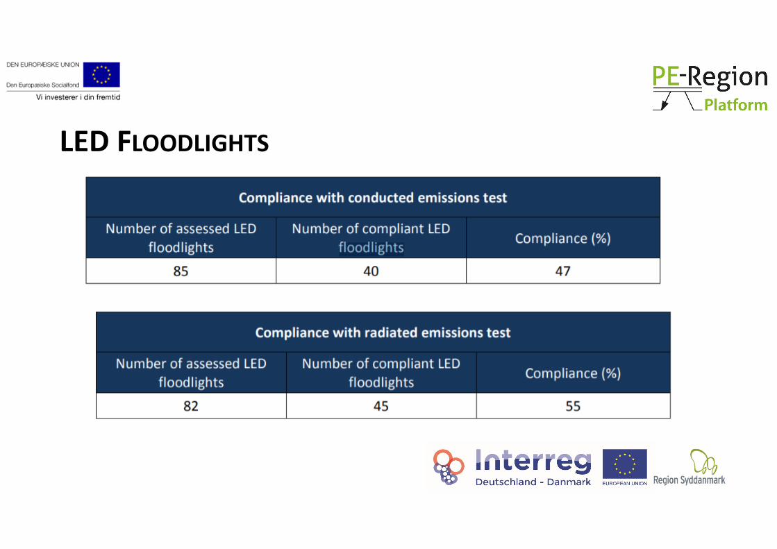
LED FLOODLIGHTS
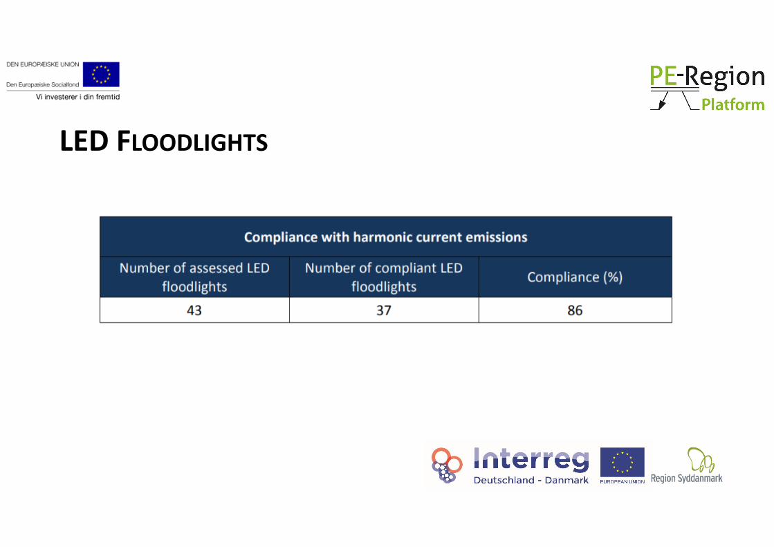
LED FLOODLIGHTS

• Compact fully anechoic room for (pre‐compliance) radiated emission and spurious emission up to 26 GHz.
• Radiated immunity measurements up to 6 GHz.
• Multi‐axis turntable for antenna measurements (passive, OTA etc.).
• Spurious emission measurements.
Our Laboratory per 1 August

• Conducted emission test in hard shielded room.
• ESD, surge, burst, voltage dip and harmonic power test stations.
• Near‐field scanner.• Various simulation tools
(restricted licenses for research purposes). Commercial license can be rented.
• 4 port 40 GHz VNA.
Our Laboratory per 1 August
EMC Services Starting From 1 August 2020• EMC do-it-yourselves test• EMC testing services by our technical staff• Consulting and analysis of test results by our experts/researchers• Remember, we are not accredited • We have equipment for all common EMC test including radiated emission and
immunity, conducted emission, burst, surge, ESD, voltage dips and interruptions, harmonics and flicker. In addition we have equipment for various antenna and throughput measurements.
• Do-it-yourselves test requires a mandatory introduction which is included in a yearly member fee.
• Prices will be market level. Details will be announced later.

Thank You
See you (hopefully) IRL in October