256 soc fpga embedded development suite user guide · 1. introduction to the intel® soc fpga eds...
TRANSCRIPT

Intel® SoC FPGA EmbeddedDevelopment Suite User Guide
Updated for Intel® Quartus® Prime Design Suite: 18.1
SubscribeSend Feedback
ug-1137 | 2018.09.24Latest document on the web: PDF | HTML

Contents
1. Introduction to the Intel® SoC FPGA EDS........................................................................41.1. Tool Versions.........................................................................................................41.2. Differences Between Standard and Professional Editions............................................. 51.3. Overview..............................................................................................................5
1.3.1. Linux Device Tree Binary.............................................................................61.3.2. Intel Stratix 10 SoC Golden Hardware Reference Design................................. 6
1.4. Hardware and Software Development Roles.............................................................. 71.4.1. Hardware Engineer.................................................................................... 81.4.2. BareMetal and RTOS Developer................................................................... 81.4.3. Linux Kernel and Driver Developer............................................................... 81.4.4. Linux Application Developer........................................................................ 9
1.5. Hardware – Software Development Flow...................................................................91.6. Introduction to the Intel SoC FPGA EDS Revision History...........................................10
2. Installing the Intel SoC FPGA EDS................................................................................112.1. Installation Folders...............................................................................................112.2. Installing the SoC EDS on Windows........................................................................112.3. Installing the Arm Development Studio 5 (DS-5) Intel SoC FPGA Edition Toolkit........... 122.4. Installing the Intel SoC FPGA EDS Document Revision History....................................12
3. Intel SoC FPGA EDS Licensing....................................................................................... 143.1. Getting the License.............................................................................................. 143.2. Activating the License...........................................................................................153.3. Intel SoC FPGA EDS Licensing Revision History........................................................ 20
4. Embedded Command Shell............................................................................................224.1. Embedded Command Shell Revision History............................................................ 22
5. Getting Started Guides..................................................................................................235.1. Getting Started Guides Revision History.................................................................. 23
6. Arm Development Studio 5 Intel SoC FPGA Edition....................................................... 246.1. Starting Eclipse Arm Development Studio 5 Intel SoC FPGA Edition.............................246.2. BareMetal Project Management..............................................................................25
6.2.1. BareMetal Project Management Using Makefiles........................................... 256.2.2. GCC-Based BareMetal Project Management................................................. 286.2.3. Arm Compiler 5 BareMetal Project Management........................................... 32
6.3. Debugging.......................................................................................................... 406.3.1. Accessing Debug Configurations.................................................................406.3.2. Creating a New Debug Configuration.......................................................... 406.3.3. Debug Configuration Options..................................................................... 426.3.4. DTSL Options.......................................................................................... 49
6.4. Arm Development Studio 5 Intel SoC FPGA Edition Revision History............................53
7. Boot Tools User Guide...................................................................................................547.1. Introduction........................................................................................................547.2. BSP Generator.....................................................................................................55
7.2.1. BSP Generation Flow................................................................................ 557.2.2. BSP Generator Graphical User Interface...................................................... 58
Contents
Intel® SoC FPGA Embedded Development Suite User Guide Send Feedback
2

7.2.3. BSP Generator Command Line Interface......................................................597.2.4. BSP Files and Folders............................................................................... 627.2.5. BSP Settings........................................................................................... 62
7.3. Bootloader Image Tool (mkpimage)........................................................................717.3.1. Operation............................................................................................... 717.3.2. Header File Format...................................................................................727.3.3. Tool Usage.............................................................................................. 737.3.4. Output Image Layout............................................................................... 74
7.4. U-Boot Image Tool (mkimage)...............................................................................767.4.1. Tool Options............................................................................................777.4.2. Usage Examples...................................................................................... 77
7.5. Building the Bootloader.........................................................................................777.5.1. Building the Cyclone V SoC and Arria V SoC Preloader...................................777.5.2. Building the Intel Arria 10 SoC Bootloader...................................................797.5.3. Building the Intel Stratix 10 SoC Bootloader................................................ 81
7.6. Boot Tools User Guide Revision History................................................................... 82
8. Hardware Library.......................................................................................................... 838.1. Feature Description.............................................................................................. 84
8.1.1. SoC Abstraction Layer (SoCAL).................................................................. 848.1.2. HW Manager........................................................................................... 84
8.2. Hardware Library Reference Documentation............................................................ 858.3. System Memory Map............................................................................................858.4. Hardware Library Revision History..........................................................................86
9. HPS Flash Programmer User Guide............................................................................... 879.1. HPS Flash Programmer Command-Line Utility.......................................................... 889.2. How the HPS Flash Programmer Works................................................................... 889.3. Using the Flash Programmer from the Command Line............................................... 88
9.3.1. HPS Flash Programmer............................................................................. 889.3.2. HPS Flash Programmer Command Line Examples......................................... 90
9.4. Supported Memory Devices...................................................................................919.5. HPS Flash Programmer User Guide Revision History..................................................92
10. BareMetal Compilers................................................................................................... 9310.1. Arm BareMetal Compilers....................................................................................9310.2. Mentor Code Sourcery Compiler........................................................................... 9310.3. BareMetal Compilers Revision History................................................................... 94
11. SD Card Boot Utility.................................................................................................... 9611.1. Usage Scenarios................................................................................................ 9611.2. Tool Options...................................................................................................... 9711.3. SD Card Boot Utility Revision History.................................................................... 98
12. Linux Software Development Tools............................................................................. 9912.1. Linux Compiler.................................................................................................. 9912.2. Linux Device Tree Generator.............................................................................. 10012.3. Linux Software Development Tools Revision History.............................................. 101
13. Support and Feedback.............................................................................................. 10213.1. Support and Feedback Revision History............................................................... 102
Contents
Send Feedback Intel® SoC FPGA Embedded Development Suite User Guide
3

1. Introduction to the Intel® SoC FPGA EDSThe Intel® SoC FPGA Embedded Development Suite (SoC EDS) is a comprehensivetool suite for embedded software development on Intel FPGA SoC devices.
The SoC EDS contains development tools, utility programs, run-time software, andapplication examples that enable firmware and application software development onIntel SoC hardware platforms.
The SoC EDS is offered in two editions:
• SoC EDS Standard Edition—The SoC EDS Standard Edition targets the Arria® VSoC, Cyclone® V SoC, and Intel Arria 10 SoC and must be used only with FPGAprojects created in Intel Quartus® Prime Standard Edition. Although the IntelFPGA SoC devices and Intel Quartus Prime Standard Edition support Intel Arria 10SoC, it is recommended to use the SoC EDS Professional Edition of both tools fornew Intel Arria 10 SoC Projects.
• SoC EDS Professional Edition—The SoC EDS Professional Edition targets theIntel Arria 10 SoC and the Intel Stratix® 10 SoC and must be used only with FPGAprojects created in Intel Quartus Prime Pro Edition.
Note: The SoC EDS Professional Edition does not support Cyclone V SoC and ArriaV SoC, as they are not supported by Intel Quartus Prime Pro Edition.
Related Information
• SoCEDSGettingStartedFor more information about getting started, refer to the SoCEDSGettingStartedpage on the Intel FPGA Wiki.
• Intel SoC FPGA EDS Licensing on page 14
1.1. Tool Versions
Table 1. Tool VersionsRefer to this table when you want to determine the tool versions.
Tool Version
Mentor Graphics* BareMetal GCC Compiler 6.2.0 (Sourcery CodeBench Lite 2016.11-88)
Linux* Compiler 4.8.3 (Linaro* GCC 4.8-2014.04)
Arm* Compiler 5 5.06 update 6
Arm Compiler 6 6.10.1
Arm Development Studio 5* (DS-5*) Intel SoC FPGA Edition 5.29.1
ug-1137 | 2018.09.24
Send Feedback
Intel Corporation. All rights reserved. Intel, the Intel logo, Altera, Arria, Cyclone, Enpirion, MAX, Nios, Quartusand Stratix words and logos are trademarks of Intel Corporation or its subsidiaries in the U.S. and/or othercountries. Intel warrants performance of its FPGA and semiconductor products to current specifications inaccordance with Intel's standard warranty, but reserves the right to make changes to any products and servicesat any time without notice. Intel assumes no responsibility or liability arising out of the application or use of anyinformation, product, or service described herein except as expressly agreed to in writing by Intel. Intelcustomers are advised to obtain the latest version of device specifications before relying on any publishedinformation and before placing orders for products or services.*Other names and brands may be claimed as the property of others.
ISO9001:2015Registered

1.2. Differences Between Standard and Professional Editions
The main difference between the two different editions exists in the SoC devices thatare supported, as mentioned in the previous section.
Things to know about installation and licensing for the two editions:
• The default installation paths are different between editions. For details on thedefault installation paths, refer to the "Installing the Intel SoC FPGA EDS" chapter.
• There are no licensing differences between SoC EDS editions. The same DS-5 IntelSoC FPGA Edition License will work for both Standard and Pro editions. For detailsabout licensing, refer to the "Intel SoC FPGA EDS Licensing" chapter.
Related Information
• Installing the Intel SoC FPGA EDS on page 11
• Intel SoC FPGA EDS Licensing on page 14
• Linux Compiler on page 99
1.3. Overview
The SoC EDS enables you to perform all required software development taskstargeting the Intel FPGA SoCs, including:
• Board bring-up
• Device driver development
• Operating system (OS) porting
• BareMetal application development and debugging
• OS- and Linux-based application development and debugging
• Debug systems running symmetric multiprocessing (SMP)
• Debug software targeting soft IP residing on the FPGA portion of the device
The major components of the SoC EDS include:
• Arm Development Studio 5 Intel SoC FPGA Edition AE Toolkit
• Compiler tool chains:
— BareMetal GNU Compiler Collection (GCC) tool chain from Mentor Graphics
— Arm BareMetal compiler 5
— Arm BareMetal compiler 6
— Linux GCC compiler tool chain from Linaro
• SoC Hardware Library (HWLIB)
• Hardware-to-software interface utilities:
— Second stage bootloader generator
— Linux device tree generator
• Sample applications
1. Introduction to the Intel® SoC FPGA EDS
ug-1137 | 2018.09.24
Send Feedback Intel® SoC FPGA Embedded Development Suite User Guide
5

• Golden Hardware Reference Designs (GHRD) including:
— FPGA hardware project
— FPGA hardware SRAM Object File (.sof) file
— Precompiled Bootloaders
• Preloader and bootloader for Arria V SoC and Cyclone V SoC
• Bootloader for Intel Arria 10 SoC
• Bootloader for Intel Stratix 10 SoC
• Embedded command shell allowing easy invocation of the included tools
• SD Card Boot Utility
• Intel Quartus Prime Programmer and Signal Tap
Note: The Golden Hardware Reference Design (GHRD) included with the SoC EDS is not anofficial release and is intended to be used only as an example. For developmentpurposes, use the official GHRD release described in the Golden System ReferenceDesign User Manual available on the Rocketboards website.
Related Information
• Golden System Reference Design User Manual
• GitHub Repository
1.3.1. Linux Device Tree Binary
SoC EDS includes Linux Device Tree Binary (DTB) files that enable Linux to load thedrivers for the IP located in the FPGA fabric:
• Cyclone V SoC: <SoC EDS installation directory>/examples/hardware/cv_soc_devkit_ghrd/soc_system.dtb
• Arria V SoC: <SoC EDS installation directory>/examples/hardware/av_soc_devkit_ghrd/ghrd_5astfd5k3.dtb
• Intel Arria 10 SoC: <SoC EDS installation directory>/examples/hardware/a10_soc_devkit_ghrd/ghrd_10as066n2.dtb
Note: These files are created with the aid of the Linux Device Tree Generator.
Note: A DTB file is not provided for Intel Stratix 10 SoC, as it is not supported by the LinuxDevice Tree Generator.
Related Information
Linux Device Tree Generator on page 100
1.3.2. Intel Stratix 10 SoC Golden Hardware Reference Design
The GHRD included with the SoC EDS v18.0 targets the device 1SX280LU2F50E2VG,while the customer-available Intel Stratix 10 SoC Development Kits are populated withthe device 1SX280LU2F50E2VGS2. The GHRD can be updated to match the device
1. Introduction to the Intel® SoC FPGA EDS
ug-1137 | 2018.09.24
Intel® SoC FPGA Embedded Development Suite User Guide Send Feedback
6

on the Intel Stratix 10 SoC Development Kit with the following commands executedfrom an Embedded Command Shell on a Linux computer where both SoC EDSProfessional Edition 18.0 and Intel Quartus Prime Pro Edition 18.0 are installed:
mkdir s10_soc_devkit_ghrdcd s10_soc_devkit_ghrdtar xf $SOCEDS_DEST_ROOT/examples/hardware/ \s10_soc_devkit_ghrd/tgz/*.tar.gzsed -i 's/QUARTUS_DEVICE := 1SX280LU2F50E2VG/QUARTUS_DEVICE \:= 1SX280LU2F50E2VGS2/g' Makefilemake cleanmake scrub_cleanrm -rf output_files qsys_top subsys_periph subsys_jtg_mst \ip/qsys_top/ ip/subsys_jtg_mst/ ip/subsys_periph/ *.qsys *.qpf *.qsfmake generate_from_tclmake sof
1.4. Hardware and Software Development Roles
Depending on your role in hardware or software development, you need a differentsubset of the SoC EDS toolkit. The following table lists some typical engineeringdevelopment roles and indicates the tools that each role typically requires.
For more information about each of these tools, refer to the Intel SoC FPGAEmbedded Development Suite page.
Table 2. Hardware and Software Development RolesThis table lists typical tool usage, but your actual requirements depend on your specific project andorganization.
Tool HardwareEngineer
BareMetalDeveloper
RTOSDeveloper
Linux Kerneland DriverDeveloper
LinuxApplicationDeveloper
Arm DS-5 Intel SoC FPGAEdition Debugging
√ √ √ √ √
Arm DS-5 Intel SoC FPGAEdition Tracing
√ √ √
Arm DS-5 Intel SoC FPGAEdition Cross Triggering
√ √ √
Hardware Libraries √ √ √
Second Stage BootloaderGenerator
√ √ √ √
Flash Programmer √ √ √ √
BareMetal Compiler √ √ √ √
Linux Compiler √ √
Linux Device Tree Generator √
Related Information
SoC Embedded Development Suite web page
1. Introduction to the Intel® SoC FPGA EDS
ug-1137 | 2018.09.24
Send Feedback Intel® SoC FPGA Embedded Development Suite User Guide
7

1.4.1. Hardware Engineer
As a hardware engineer, you typically design the FPGA hardware in Qsys. You can usethe debugger of Arm DS-5 Intel SoC FPGA Edition AE to connect to the Arm cores andtest the hardware. A convenient feature of the DS-5 debugger is the soft IP registervisibility, using Cortex Microcontroller Software Interface Standard (CMSIS) SystemView Description (.svd) files. With this feature, you can easily read and modify thesoft IP registers from the Arm side.
As a hardware engineer, you may generate the Preloader for your hardwareconfiguration. The Preloader is a piece of software that configures the HPS componentaccording to the hardware design.
As a hardware engineer, you may also perform the board bring-up. You can use ArmDS-5 Intel SoC FPGA Edition debugger to verify that they can connect to the Arm andthe board is working correctly.
These tasks require JTAG debugging, which is enabled only in the Arm DS-5 Intel SoCFPGA Edition, which is part of the paid Intel Intel SoC FPGA EDS license.
For more information, see the "Intel SoC FPGA EDS Licensing" section.
Related Information
• Intel SoC FPGA EDS Licensing on page 14
• Hardware – Software Development Flow on page 9
1.4.2. BareMetal and RTOS Developer
As a BareMetal or a RTOS developer, you need JTAG debugging and low-level visibilityinto the system. The following tasks require JTAG debugging, which is enabled only inthe Arm DS-5 Intel SoC FPGA Edition.
• To compile your code and the SoC Hardware Library to control the hardware in aconvenient and consistent way, use the BareMetal compiler.
• To program the flash memory on the target board, use the Flash Programmer.
For more information, see the "Licensing" section.
Related Information
Intel SoC FPGA EDS Licensing on page 14
1.4.3. Linux Kernel and Driver Developer
As a Linux kernel or driver developer, you may use the same tools the RTOSdevelopers use, because you need low-level access and visibility into the system.However, you must use the Linux compiler instead of the BareMetal compiler. You canuse the Linux device tree generator (DTG) to generate Linux device trees.
These tasks require JTAG debugging, which is enabled only in the Arm DS-5 Intel SoCFPGA Edition.
For more information, see the "Licensing" section.
1. Introduction to the Intel® SoC FPGA EDS
ug-1137 | 2018.09.24
Intel® SoC FPGA Embedded Development Suite User Guide Send Feedback
8

Related Information
Intel SoC FPGA EDS Licensing on page 14
1.4.4. Linux Application Developer
As a Linux application developer, you write code that targets the Linux OS running onthe board. Because the OS provides drivers for all the hardware, you do not need low-level visibility over JTAG. DS-5 offers a very detailed view of the OS, showinginformation about the threads that are running and the drivers that are loaded.
These tasks do not require JTAG debugging. You can perform these tasks with boththe paid and free SoC EDS FPGA licenses. For more information, see the "Licensing"section.
Related Information
Intel SoC FPGA EDS Licensing on page 14
1.5. Hardware – Software Development Flow
The Intel hardware-to-software handoff utilities allow hardware and software teams towork independently and follow their respective familiar design flows.
Figure 1. Intel Hardware-to-Software Handoff
ACDSHardware Design
Handoff
.svd
.sopcinfo
Bootloader Generator
Bootloader
Linux Device Tree Generator
Linux Device Tree
Ds-5 Debugger
.sof
1. Introduction to the Intel® SoC FPGA EDS
ug-1137 | 2018.09.24
Send Feedback Intel® SoC FPGA Embedded Development Suite User Guide
9

The following handoff files are created when the hardware project is compiled:
• Handoff folder – contains information about how the HPS component isconfigured, including things like which peripherals are enabled, the pin MUXingand IOCSR settings, and memory parameters. The handoff folder is used by thesecond stage bootloader generator to create the preloader.
For more information about the handoff folder, refer to the "BSP Generation Flow"section.
• .svd file – contains descriptions of the HPS registers and of the soft IP registers onthe FPGA side implemented in the FPGA portion of the device. The .svd filecontains register descriptions for the HPS peripheral registers and soft IPcomponents in the FPGA portion of the SoC. This file is used by the Arm DS-5 IntelSoC FPGA Edition Debugger to allow you to inspect and modify these registers.
• .sopcinfo file – contains a description of the entire system. The SOPC Information(.sopcinfo) file, containing a description of the entire system, is used by the Linuxdevice tree generator to create the device tree used by the Linux kernel.
For more information, refer to the "Linux Device Tree Generator" section.
Note: The soft IP register descriptions are not generated for all soft IP cores.
Note: For Intel Stratix 10 SoC, the handoff information is part of the configurationbitstream, and the bootloader has direct access to it. Because of that thereis no need for a Bootloader Generator tool in this case.
Related Information
• BSP Generation Flow on page 55
• SoC Embedded Development Suite Download Page
• Linux Device Tree Generator on page 100
1.6. Introduction to the Intel SoC FPGA EDS Revision History
Document Version Changes
2018.09.24 Updated the Tool versions for Arm Compiler 6 and Arm Development Studio 5(DS-5) Intel SoC FPGA Edition
2018.06.18 • Updated chapter to include support for Intel Stratix 10 SoC• Replaced "Second Stage Bootloader" with "Bootloader".• For the Golden Hardware Reference Designs (GHRD), added the precompiled
bootloader for Intel Stratix 10 SoC• Added the "Intel Stratix 10 SoC Golden Hardware Reference Design" section
2017.05.08 • Intel FPGA rebranding• Rebranded paths and tools for the Standard and Professional versions
2016.11.07 Maintenance release
2016.05.27 Renamed the Web and Subscription Editions to align with Quartus Prime naming
2016.02.17 Maintenance release
2015.08.06 Added Intel Arria 10 SoC support
1. Introduction to the Intel® SoC FPGA EDS
ug-1137 | 2018.09.24
Intel® SoC FPGA Embedded Development Suite User Guide Send Feedback
10

2. Installing the Intel SoC FPGA EDSYou must install the SoC EDS and the Arm DS-5 Intel SoC FPGA Edition in order to runthe SoC EDS on an Intel SoC hardware platform.
2.1. Installation Folders
The default installation folder for SoC EDS, referred to as <SoC FPGA EDS installationdirectory> throughout this document, is:
• Standard Edition:
— c:\intelFPGA\18.0\embedded on Windows
— ~/intelFPGA/18.0/embedded on Linux
• Professional Edition:
— c:\intelFPGA_pro\18.0\embedded on Windows
— ~/intelFPGA_pro/18.0/embedded on Linux
The default installation folder for the Intel Quartus Prime Programmer, referred to as<Quartus Prime installation directory> throughout this document, is:
• Standard Edition:
— c:\intelFPGA\18.0\qprogrammer on Windows
— ~/intelFPGA/18.0/qprogrammer on Linux
• Professional Edition:
— c:\intelFPGA_pro\18.0\qprogrammer on Windows
— ~/intelFPGA_pro/18.0/qprogrammer on Linux
2.2. Installing the SoC EDS on Windows
Perform the following steps to install the SoC EDS Tool Suite in a Windows-basedsystem:
1. Download the latest installation program from the Intel SoC FPGA EmbeddedDevelopment Suite Download Center page of the Intel FPGA website.
2. Run the installer to open the Installing Intel SoC FPGA EmbeddedDevelopment Suite (EDS) dialog box, and click Next to start the SetupWizard.
3. Accept the license agreement, and click Next.
4. Accept the default installation directory or browse to another installation directory,and click Next.
ug-1137 | 2018.09.24
Send Feedback
Intel Corporation. All rights reserved. Intel, the Intel logo, Altera, Arria, Cyclone, Enpirion, MAX, Nios, Quartusand Stratix words and logos are trademarks of Intel Corporation or its subsidiaries in the U.S. and/or othercountries. Intel warrants performance of its FPGA and semiconductor products to current specifications inaccordance with Intel's standard warranty, but reserves the right to make changes to any products and servicesat any time without notice. Intel assumes no responsibility or liability arising out of the application or use of anyinformation, product, or service described herein except as expressly agreed to in writing by Intel. Intelcustomers are advised to obtain the latest version of device specifications before relying on any publishedinformation and before placing orders for products or services.*Other names and brands may be claimed as the property of others.
ISO9001:2015Registered

Note: It is recommended to accept the default installation paths for both IntelQuartus Prime and SoC EDS software, to allow them to properly operatetogether.
5. Select All the components to be installed, and click Next. The installer displays asummary of the installation.
6. Click Next to start the installation process. The installer displays a separate dialogbox with the installation progress of the component installation.
7. When the installation is complete, turn on Launch DS-5 Installation to start theArm DS-5 Intel SoC FPGA Edition installation, and click Finish.
Note: On some Linux-based machines, you can install the SoC EDS with a setup GUI similarto the Windows-based setup GUI. Because of the variety of Linux distributions andpackage requirements, not all Linux machines can use the setup GUI. If the GUI is notavailable, use an equivalent command-line process. Download the Linux installationprogram from the Intel SoC FPGA Embedded Development Suite Download Centerpage on the Intel FPGA website.
Related Information
SoC Embedded Development Suite Download Center
2.3. Installing the Arm Development Studio 5 (DS-5) Intel SoCFPGA Edition Toolkit
For the last step of the SoC EDS installation process, start theArm Development Studio 5 Intel SoC FPGA Edition Toolkit installer.
Note: Make sure you have the proper setting to access the internet.
1. When the Welcome message is displayed, click Next.
2. Accept the license agreement and click Next.
3. Accept the default installation path, to ensure proper interoperability between SoCEDS and Arm Development Studio 5 Intel SoC FPGA Edition, and click Next.
4. Click Install to start the installation process. The progress bar is displayed.
5. When a driver installation window appears, click Next.
6. Accept the driver installation and click Install.
7. After successful installation, click Finish.Arm Development Studio 5 Intel SoC FPGA Edition installation is complete.
8. Click Finish.
2.4. Installing the Intel SoC FPGA EDS Document Revision History
Document Version Changes
2018.09.24 Updated the path names to coincide with the 18.1 release.
2018.06.18 Maintenance release
2018.05.07 Maintenance release
continued...
2. Installing the Intel SoC FPGA EDS
ug-1137 | 2018.09.24
Intel® SoC FPGA Embedded Development Suite User Guide Send Feedback
12

Document Version Changes
2017.05.08 • Intel FPGA rebranding• Rebranded paths and tools for the Standard and Professional versions
2016.11.07 Maintenance release
2016.05.27 Maintenance release
2016.02.17 Updated the installation path to 15.1
2015.08.06 Added Intel Arria 10 SoC support
2. Installing the Intel SoC FPGA EDS
ug-1137 | 2018.09.24
Send Feedback Intel® SoC FPGA Embedded Development Suite User Guide
13
3. Intel SoC FPGA EDS LicensingThe only SoC EDS component that requires a license is the Arm DS-5 Intel SoC FPGAEdition. The rest of the SoC EDS components, such as tools and software, do notrequire a license. This is the same for both Standard and Professional editions of SoCEDS.
The Arm DS-5 Intel SoC FPGA Edition has three different license options:
• Arm DS-5 Intel SoC FPGA Edition License
• Arm DS-5 Intel SoC FPGA Edition Community Edition License
• 30-day Evaluation of Arm DS-5 Intel SoC FPGA Edition License
The following table shows the different debugging capabilities of the Arm DS-5 IntelSoC FPGA Edition Licenses:
Table 3. Comparing Arm DS-5 Intel SoC FPGA Edition Licenses
Licensing Option Debugging Scenarios Enabled
Arm DS-5 Intel SoC FPGA Edition Community EditionLicense
• Linux application debugging over ethernet
Arm DS-5 Intel SoC FPGA Edition License, including the 30day evaluation version
• JTAG-based BareMetal Debugging• JTAG-based Linux Kernel and Driver Debugging• Linux Application Debugging over Ethernet
Based on the specific Arm DS-5 Intel SoC FPGA Edition License that is used, the SoCFPGA EDS has two different licensing options:
• SoC EDS Paid license - using Arm DS-5 Intel SoC FPGA Edition license
• SoC EDS Free license - using Arm DS-5 Intel SoC FPGA Edition Community Editionlicense
Note: For a detailed comparison chart, refer to the "Compare Editions" section on the IntelSoC FPGA Embedded Development Suite web page.
Related Information
SoC Embedded Development Suite web page
3.1. Getting the License
Depending on the licensing option, it is necessary to follow the steps detailed for eachoption to obtain the license.
ug-1137 | 2018.09.24
Send Feedback
Intel Corporation. All rights reserved. Intel, the Intel logo, Altera, Arria, Cyclone, Enpirion, MAX, Nios, Quartusand Stratix words and logos are trademarks of Intel Corporation or its subsidiaries in the U.S. and/or othercountries. Intel warrants performance of its FPGA and semiconductor products to current specifications inaccordance with Intel's standard warranty, but reserves the right to make changes to any products and servicesat any time without notice. Intel assumes no responsibility or liability arising out of the application or use of anyinformation, product, or service described herein except as expressly agreed to in writing by Intel. Intelcustomers are advised to obtain the latest version of device specifications before relying on any publishedinformation and before placing orders for products or services.*Other names and brands may be claimed as the property of others.
ISO9001:2015Registered

Arm DS-5 Intel SoC FPGA Edition License - If you have purchased a SoCdevelopment kit or a stand-alone license for DS-5 Intel SoC FPGA Edition AE, then youhave already received an Arm license serial number. This is a 15-digit alphanumericstring with two dashes in between. Use this serial number to activate your license inDS-5 Intel SoC FPGA Edition, as shown in the "Activating the License" section.
Note: This license contains one-year of Support and Maintenance from Arm starting at thedate of purchase or renewal.
DS-5 Intel SoC FPGA Edition Community Edition License - If you are using theSoC EDS Lite Edition, you are able to use the DS-5 Intel SoC FPGA Edition perpetuallyto debug Linux applications over an Ethernet connection. Get your Arm licenseactivation code from the "DS-5 Intel SoC FPGA Edition Community Edition" section onthe DS-5 Intel SoC FPGA Edition Development Studio page on the Arm website andthen activate your license in DS-5 Intel SoC FPGA Edition, as shown in the "Activatingthe License" section.
30-Day Evaluation of DS-5 Intel SoC FPGA Edition License - If you want toevaluate the DS-5 Intel SoC FPGA Edition, you can get a 30-Day Evaluation activationcode from the "DS-5 Intel SoC FPGA Edition 30-Day Evaluation" section on the DS-5Intel SoC FPGA Edition Development Studio page on the Arm website and thenactivate your license in Arm DS-5 Intel SoC FPGA Edition, as shown in the "Activatingthe License" section.
Related Information
• SoC FPGA EDS Download Page
• Activating the License on page 15
• DS-5 Community Edition LicenseFor more information about obtaining your ARM license activation code for theDS-5 Community Edition license
• DS-5 Intel FPGA Edition 30-Day EvaluationFor more information about obtaining your activation code for the DS-5 IntelFPGA Edition 30-Day Evaluation license
3.2. Activating the License
This section presents the steps required for activating the license in the Arm DS-5Intel SoC FPGA Edition by using the serial license number or activation code that werementioned in the "Getting the License" chapter.
Note: An active user account is required to activate the Arm DS-5 Intel SoC FPGA Edition AElicense. If you do not have an active user account, it can be created on the Arm Self-Service page available on the Arm website.
1. The first time the Arm DS-5 Intel SoC FPGA Edition is run, it notifies you that itrequires a license. Click the Open License Manager button.
3. Intel SoC FPGA EDS Licensing
ug-1137 | 2018.09.24
Send Feedback Intel® SoC FPGA Embedded Development Suite User Guide
15

Figure 2. No License Found
2. If at any time it is required to change the license, select Help ➤ Arm LicenseManager to open the License Manager.
Figure 3. Accessing Arm License Manager
3. The License Manager - View and edit licenses dialog box opens and showsthat a license is not available. Click the Add License button.
3. Intel SoC FPGA EDS Licensing
ug-1137 | 2018.09.24
Intel® SoC FPGA Embedded Development Suite User Guide Send Feedback
16

Figure 4. Arm License Manager
4. In the Add License - Obtain a new licenses dialog box, select the type oflicense to enter. In this example, select the radio button, “Enter a serial numberor activation code to obtain a license” to enter the choices listed, below. Whendone, click Enter.
a. Arm DS-5 Intel SoC FPGA Edition—Enter the Arm License Number.
b. Arm DS-5 Intel SoC FPGA Edition Community Edition and 30-day Evaluation ofArm DS-5 Intel SoC FPGA Edition—Enter the Arm License Activation Code.
3. Intel SoC FPGA EDS Licensing
ug-1137 | 2018.09.24
Send Feedback Intel® SoC FPGA Embedded Development Suite User Guide
17

Figure 5. Add License - Obtain a New License
5. Click Next.
6. In the Add License - Choose Host ID dialog box, select the Host ID (NetworkAdapter MAC address) to tie the license to. If there are more than one option,select the one you desire to lock the license to, and click Next.
3. Intel SoC FPGA EDS Licensing
ug-1137 | 2018.09.24
Intel® SoC FPGA Embedded Development Suite User Guide Send Feedback
18

Figure 6. Add License - Choose host ID
7. In the Add License - Developer account details dialog box, enter an Armdeveloper (Silver) account. If you do not have an account, it can be created easilyby clicking the provided link. After entering the account information, click Finish.
Figure 7. Add License - Developer Account Details
Note: The License Manager needs to be able to connect to the Internet in order toactivate the license. If you do not have an Internet connection, you willneed to write down your Ethernet MAC address and generate the licensedirectly from the Arm Self-Service web page on the Arm website, thenselect the "Already have a license" option in the License Manger.
3. Intel SoC FPGA EDS Licensing
ug-1137 | 2018.09.24
Send Feedback Intel® SoC FPGA Embedded Development Suite User Guide
19

Note: Only the Arm DS-5 Intel SoC FPGA Edition, with an associated licensenumber can be activated this way. The Arm DS-5 Intel SoC FPGA EditionCommunity Edition and 30-day Evaluation of Arm DS-5 Intel SoC FPGAEdition are based on activation codes, and these codes cannot be used onthe Arm Self-Service web page on the Arm website. They need to beentered directly in the License Manager; which means an Internetconnection is a requirement for licensing.
The Arm License Manager uses the Eclipse settings to connect to the Internet. Thedefault Eclipse settings use the system-wide configuration for accessing theInternet. In case the License Manager cannot connect to the Internet, you can tryto change the Proxy settings by going to Window ➤ Preferences ➤ General ➤Network Connections. Ensure that "HTTPS" proxy entry is configured andenabled.
8. After a few moments, the Arm DS-5 Intel SoC FPGA Edition will activatethe license and display it in the License Manager. Click Close.
Figure 8. Arm License Manager
Related Information
• ARM website
• Getting the License on page 14
3.3. Intel SoC FPGA EDS Licensing Revision History
Document Version Changes
2018.09.24 Maintenance release
2018.06.18 Maintenance release
continued...
3. Intel SoC FPGA EDS Licensing
ug-1137 | 2018.09.24
Intel® SoC FPGA Embedded Development Suite User Guide Send Feedback
20

Document Version Changes
2017.05.08 • Intel FPGA rebranding• Rebranded paths and tools for the Standard and Professional versions
2016.11.07 Maintenance release
2016.05.27 Renamed the Web and Subscription Editions to align with Quartus Prime naming
2016.02.17 Maintenance release
2015.08.06 Added Intel Arria 10 SoC support
3. Intel SoC FPGA EDS Licensing
ug-1137 | 2018.09.24
Send Feedback Intel® SoC FPGA Embedded Development Suite User Guide
21

4. Embedded Command ShellThe purpose of the embedded command shell is to enable you to invoke the SoC EDStools. It enables you to invoke the SoC EDS tools without qualifying them with the fullpath. Commands like eclipse, bsp-editor, or arm-altera-eabi-gcc can beexecuted directly.
On Windows, the embedded command shell is started from the Start menu or byrunning:
<SoC EDS installation directory>\Embedded_Command_Shell.bat
On Linux, the embedded command shell is started by running:
<SoC EDS installation directory>/embedded_command_shell.sh
4.1. Embedded Command Shell Revision History
Document Version Changes
2018.09.24 Maintenance release
2018.06.18 Maintenance release
2017.05.08 • Intel FPGA rebranding• Rebranded paths and tools for the Standard and Professional versions
2016.11.07 Maintenance release
2016.05.27 Maintenance release
2016.02.17 Maintenance release
2015.08.06 Added Intel Arria 10 SoC support
ug-1137 | 2018.09.24
Send Feedback
Intel Corporation. All rights reserved. Intel, the Intel logo, Altera, Arria, Cyclone, Enpirion, MAX, Nios, Quartusand Stratix words and logos are trademarks of Intel Corporation or its subsidiaries in the U.S. and/or othercountries. Intel warrants performance of its FPGA and semiconductor products to current specifications inaccordance with Intel's standard warranty, but reserves the right to make changes to any products and servicesat any time without notice. Intel assumes no responsibility or liability arising out of the application or use of anyinformation, product, or service described herein except as expressly agreed to in writing by Intel. Intelcustomers are advised to obtain the latest version of device specifications before relying on any publishedinformation and before placing orders for products or services.*Other names and brands may be claimed as the property of others.
ISO9001:2015Registered

5. Getting Started GuidesThe Getting Started Guides chapter provides instructions on how to access completeGetting Started instructions including the following:
• Board Setup
• Running the Tools
• Second Stage Bootloader
• Baremetal Debugging
• Hardware Libraries (HWLibs)
• Peripheral Register Visibility
• Baremetal Project Management
• Linux Application Debugging
• Linux Kernel and Driver Debugging
• Tracing
Related Information
SoCEDSGettingStartedFor more information about getting started, refer to the SoCEDSGettingStartedpage on the Intel FPGA Wiki.
5.1. Getting Started Guides Revision History
Document Version Changes
2018.09.24 Maintenance release
2018.06.18 Maintenance release
2017.05.08 • Intel FPGA rebranding• Rebranded paths and tools for the Standard and Professional versions
2016.11.07 Maintenance release
2016.05.27 Maintenance release
2016.02.17 Maintenance release
2015.08.06 Removed content from this section and moved it to the Intel FPGA Wiki
ug-1137 | 2018.09.24
Send Feedback
Intel Corporation. All rights reserved. Intel, the Intel logo, Altera, Arria, Cyclone, Enpirion, MAX, Nios, Quartusand Stratix words and logos are trademarks of Intel Corporation or its subsidiaries in the U.S. and/or othercountries. Intel warrants performance of its FPGA and semiconductor products to current specifications inaccordance with Intel's standard warranty, but reserves the right to make changes to any products and servicesat any time without notice. Intel assumes no responsibility or liability arising out of the application or use of anyinformation, product, or service described herein except as expressly agreed to in writing by Intel. Intelcustomers are advised to obtain the latest version of device specifications before relying on any publishedinformation and before placing orders for products or services.*Other names and brands may be claimed as the property of others.
ISO9001:2015Registered
6. Arm Development Studio 5 Intel SoC FPGA EditionThe Arm DS-5 Intel SoC FPGA Edition is a device-specific exclusive offering from Intel;and is a powerful Eclipse-based comprehensive Integrated Development Environment(IDE).
For the current version, refer to Table 1 on page 4.
Some of the most important provided features are:
• File editing, supporting syntax highlighting and source code indexing
• Build support, based on makefiles
• BareMetal debugging
• Linux application debugging
• Linux kernel and driver debugging
• Multicore debugging
• Access to HPS peripheral registers
• Access to FPGA soft IP peripheral registers
• Tracing of program execution through Program Trace Macrocells (PTM)
• Tracing of system events through System Trace Macrocells (STM)
• Cross-triggering between HPS and FPGA
• Connecting to the target using Intel FPGA Download Cable II
The Arm Development Studio 5 Intel SoC FPGA Edition is a complex tool with manyfeatures and options. This chapter only describes the most common features andoptions and provides getting started scenarios to help you get started, quickly.
You can access the Arm Development Studio 5 Intel SoC FPGA Edition referencematerial from Eclipse, by navigating to Help ➤ Help Contents ➤ Arm DS-5 IntelSoC FPGA Edition Documentation or on the Arm website.
Related Information
• Online ARM DS-5 DocumentationThe ARM DS-5 for Intel SoC FPGA reference material can be accessed online onthe documentation page of the ARM website.
• Tool Versions on page 4
6.1. Starting Eclipse Arm Development Studio 5 Intel SoC FPGAEdition
Arm Development Studio 5 Intel SoC FPGA Edition must be started from theEmbedded Command Shell.
ug-1137 | 2018.09.24
Send Feedback
Intel Corporation. All rights reserved. Intel, the Intel logo, Altera, Arria, Cyclone, Enpirion, MAX, Nios, Quartusand Stratix words and logos are trademarks of Intel Corporation or its subsidiaries in the U.S. and/or othercountries. Intel warrants performance of its FPGA and semiconductor products to current specifications inaccordance with Intel's standard warranty, but reserves the right to make changes to any products and servicesat any time without notice. Intel assumes no responsibility or liability arising out of the application or use of anyinformation, product, or service described herein except as expressly agreed to in writing by Intel. Intelcustomers are advised to obtain the latest version of device specifications before relying on any publishedinformation and before placing orders for products or services.*Other names and brands may be claimed as the property of others.
ISO9001:2015Registered

Eclipse needs to be started from the Embedded Command Shell so that all the utilitiesare added to the search path, and they can be used directly from the makefileswithout the full path.
To start the Eclipse IDE that the Arm Development Studio 5 Intel SoC FPGA Editionuses, you must type eclipse & at the command line.
6.2. BareMetal Project Management
Arm Development Studio 5 Intel SoC FPGA Edition enables convenient projectmanagement for BareMetal projects using two different methods:
• Using Makefiles
• Using the Arm Development Studio 5 Intel SoC FPGA Edition graphical interface
Some users prefer Makefiles because they allow the option for the project compilationto be performed from scripts. Other users prefer to use a GUI to manage the project,and this is available for both GCC and Arm DS-5 Intel SoC FPGA Edition CompilerBareMetal projects.
Method Advantages Compiler Toolchain Support
Makefile Scripted compilation GCC
Arm Development Studio 5 Intel SoCFPGA Edition graphical interface
Multiple toolchain support GCC, Arm DS-5 Intel SoC FPGA EditionCompiler
6.2.1. BareMetal Project Management Using Makefiles
The Arm Development Studio 5 Intel SoC FPGA Edition enables convenient projectmanagement using makefiles. The sample projects that are provided with SoC EDSuse makefiles to manage the build process.
Note: This option refers to just the DS-5 Intel SoC FPGA Edition specific aspects. If you arenot familiar with defining and using makefiles, please use the Arm DevelopmentStudio 5 Intel SoC FPGA Edition GUI option detailed in the next section.
To allow Arm Development Studio 5 Intel SoC FPGA Edition to manage a makefile-based project, create a project, as follows:
1. Create a folder on the disk.
2. Create the project by selecting File ➤ New ➤ Makefile Project with ExistingCode.
6. Arm Development Studio 5 Intel SoC FPGA Edition
ug-1137 | 2018.09.24
Send Feedback Intel® SoC FPGA Embedded Development Suite User Guide
25

Figure 9. Creating a Project with Existing Code
3. Type the folder name in the Existing Code Location edit box and then clickFinish.
6. Arm Development Studio 5 Intel SoC FPGA Edition
ug-1137 | 2018.09.24
Intel® SoC FPGA Embedded Development Suite User Guide Send Feedback
26

Figure 10. Import Existing Code
4. Create a Makefile in that folder, and define the rules required for compiling thecode. Make sure it has the all and the clean targets.Arm Development Studio 5 Intel SoC FPGA Edition now offers the possibility ofinvoking the build process from the IDE and allows you to build your project, asshown in the following figure:
6. Arm Development Studio 5 Intel SoC FPGA Edition
ug-1137 | 2018.09.24
Send Feedback Intel® SoC FPGA Embedded Development Suite User Guide
27

Figure 11. Eclipse IDE - Build Process Invoked - Building a Software Project in ArmDevelopment Studio 5 Intel SoC FPGA Edition
If the compilation tools issue errors, Arm Development Studio 5 Intel SoC FPGAEdition parses and formats them for you and displays them in the Problems view.
5. Build a software project in Arm Development Studio 5 Intel SoC FPGA Edition.
6.2.2. GCC-Based BareMetal Project Management
This section shows how the BareMetal toolchain plugin can be used to manage GCC-based projects in a GUI environment.
6.2.2.1. Creating Project
1. Start Eclipse.
2. Go to File ➤ New C Project.
3. Determine if you want to create an Executable empty project or a BareMetallibrary empty project.
a. BareMetal executableSelect Project Type to be Executable ➤ Empty Project then Toolchain tobe Intel FPGA Baremetal GCC then click Finish.
6. Arm Development Studio 5 Intel SoC FPGA Edition
ug-1137 | 2018.09.24
Intel® SoC FPGA Embedded Development Suite User Guide Send Feedback
28

Figure 12. BareMetal Executable Project Type
b. Static LibrarySelect BareMetal Library ➤ Empty Project and click Finish.
6. Arm Development Studio 5 Intel SoC FPGA Edition
ug-1137 | 2018.09.24
Send Feedback Intel® SoC FPGA Embedded Development Suite User Guide
29
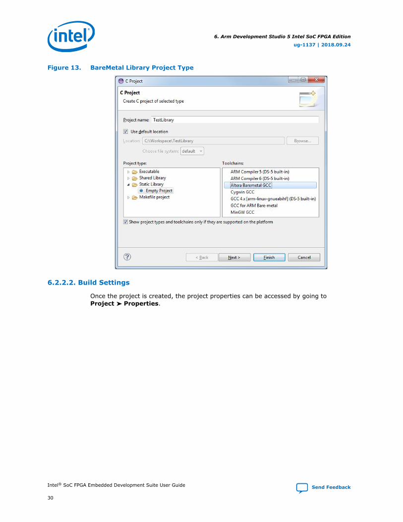
Figure 13. BareMetal Library Project Type
6.2.2.2. Build Settings
Once the project is created, the project properties can be accessed by going toProject ➤ Properties.
6. Arm Development Studio 5 Intel SoC FPGA Edition
ug-1137 | 2018.09.24
Intel® SoC FPGA Embedded Development Suite User Guide Send Feedback
30

Figure 14. Project Properties
Then, in the Project Properties window, the Compilation settings can be accessedby selecting C/C++ Build ➤ Settings.
6. Arm Development Studio 5 Intel SoC FPGA Edition
ug-1137 | 2018.09.24
Send Feedback Intel® SoC FPGA Embedded Development Suite User Guide
31

Figure 15. Project Settings
The Build Settings include detailed settings for all tools:
• Compiler
• Assembler
• Linker
The "Getting Started Guides" section in this document contains a link to completeinstructions on how to create a project from scratch, compile it and run it on an IntelSoC development board.
Related Information
Getting Started Guides on page 23
6.2.3. Arm Compiler 5 BareMetal Project Management
The Arm Compiler 5 is shipped with the SoC EDS.
For the current version, refer to Table 1 on page 4. The Arm DS-5 Intel SoC FPGAEdition can be used to manage Arm compiler projects in a GUI environment.
Related Information
Tool Versions on page 4
6. Arm Development Studio 5 Intel SoC FPGA Edition
ug-1137 | 2018.09.24
Intel® SoC FPGA Embedded Development Suite User Guide Send Feedback
32

6.2.3.1. Creating a Project
1. Start Eclipse.
2. Go to File ➤ New C Project.
3. Select one of the following options:
a. Select "Project Type" as Executable ➤ Empty Project and then for"Toolchains", select Arm Compiler 5. Click Finish.
Figure 16. Create an Empty Arm Compiler BareMetal Executable Project
b. Select Static Library ➤ Empty Project and then for "Toolchains", select ArmCompiler 5. Click Finish.
6. Arm Development Studio 5 Intel SoC FPGA Edition
ug-1137 | 2018.09.24
Send Feedback Intel® SoC FPGA Embedded Development Suite User Guide
33

Figure 17. Create an Empty Arm Compiler BareMetal Library Project
6.2.3.2. Linker Script
Arm Development Studio 5 Intel SoC FPGA Edition offers a visual tool to help createlinker scripts.
1. Go to File ➤ New ➤ Other...
6. Arm Development Studio 5 Intel SoC FPGA Edition
ug-1137 | 2018.09.24
Intel® SoC FPGA Embedded Development Suite User Guide Send Feedback
34

Figure 18. Creating a Linker Script
2. Select Scatter File Editor ➤ Scatter File and press Next.
6. Arm Development Studio 5 Intel SoC FPGA Edition
ug-1137 | 2018.09.24
Send Feedback Intel® SoC FPGA Embedded Development Suite User Guide
35

Figure 19. Creating a Scatter File
3. Select the location of the new file, type in the file name and press Finish.
6. Arm Development Studio 5 Intel SoC FPGA Edition
ug-1137 | 2018.09.24
Intel® SoC FPGA Embedded Development Suite User Guide Send Feedback
36

Figure 20. Create a New Scatter File Resource
4. The linker script file can be edited directly as shown in the example below.
6. Arm Development Studio 5 Intel SoC FPGA Edition
ug-1137 | 2018.09.24
Send Feedback Intel® SoC FPGA Embedded Development Suite User Guide
37

Figure 21. Linker Script Example
5. The file can also be edited by using the tools on the Outline view for the file.
Figure 22. Editing "Scatter.scat" File Using Tools on the Outline View
6.2.3.3. Build Settings
1. Once the project is created, the project properties can be accessed by going toProject ➤ Properties.
6. Arm Development Studio 5 Intel SoC FPGA Edition
ug-1137 | 2018.09.24
Intel® SoC FPGA Embedded Development Suite User Guide Send Feedback
38
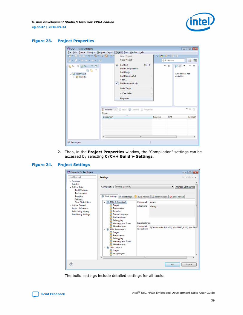
Figure 23. Project Properties
2. Then, in the Project Properties window, the "Compilation" settings can beaccessed by selecting C/C++ Build ➤ Settings.
Figure 24. Project Settings
The build settings include detailed settings for all tools:
6. Arm Development Studio 5 Intel SoC FPGA Edition
ug-1137 | 2018.09.24
Send Feedback Intel® SoC FPGA Embedded Development Suite User Guide
39

• Compiler
• Assembler
• Linker
The "Getting Started with Arm DS-5 Intel SoC FPGA Edition Compiler Bare MetalProject Management" contains a link to complete instructions on how to create aproject from scratch, compile it and run it on an Intel SoC development board.
Related Information
Getting Started Guides on page 23
6.3. Debugging
The Arm Development Studio 5 Intel SoC FPGA Edition offers you a variety ofdebugging features.
6.3.1. Accessing Debug Configurations
The settings for a debugging session are stored in a Debug Configuration. TheDebug Configurations window is accessible from the Run ➤ DebugConfigurations menu.
Figure 25. Accessing Debug Configurations
6.3.2. Creating a New Debug Configuration
A Debug Configuration is created in the Debug Configurations window byselecting DS-5 Debugger as the type of configuration in the left panel and then right-clicking with the mouse and selecting the New menu option.
6. Arm Development Studio 5 Intel SoC FPGA Edition
ug-1137 | 2018.09.24
Intel® SoC FPGA Embedded Development Suite User Guide Send Feedback
40
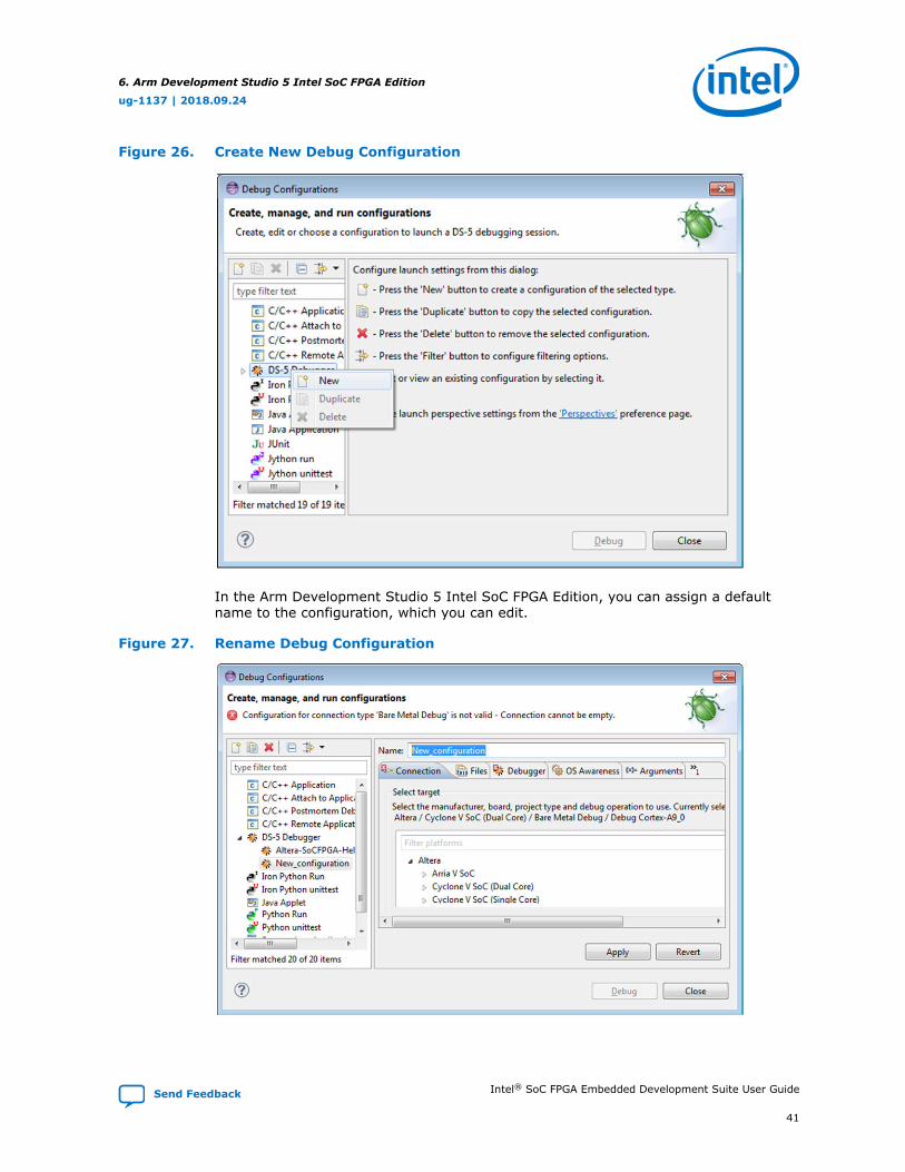
Figure 26. Create New Debug Configuration
In the Arm Development Studio 5 Intel SoC FPGA Edition, you can assign a defaultname to the configuration, which you can edit.
Figure 27. Rename Debug Configuration
6. Arm Development Studio 5 Intel SoC FPGA Edition
ug-1137 | 2018.09.24
Send Feedback Intel® SoC FPGA Embedded Development Suite User Guide
41

6.3.3. Debug Configuration Options
This section lists the Debug Configuration options, which allows you to specify thedesired debugging options for a project:
• Connection Options
• File Options
• Debugger Options
• RTOS Awareness
• Arguments
• Environment
• Event Viewer
Related Information
• SoCEDSGettingStartedFor examples on how to use the ARM DS-5 for Intel SoC FPGA debuggingfeatures, refer to the SoCEDSGettingStarted page on the Intel FPGA Wiki.
• Online ARM DS-5 DocumentationFor more information, refer to the DS-5 reference documentation located onthe ARM website.
6.3.3.1. Connection Options
The Connection tab allows you to select the desired target. You must select thedebugging target from the provided options, which cover BareMetal applications, Linuxkernel and Linux application debugging for all Intel SoC FPGA devices.
6. Arm Development Studio 5 Intel SoC FPGA Edition
ug-1137 | 2018.09.24
Intel® SoC FPGA Embedded Development Suite User Guide Send Feedback
42
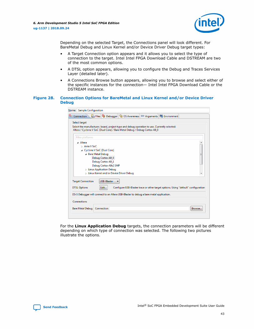
Depending on the selected Target, the Connections panel will look different. ForBareMetal Debug and Linux Kernel and/or Device Driver Debug target types:
• A Target Connection option appears and it allows you to select the type ofconnection to the target. Intel Intel FPGA Download Cable and DSTREAM are twoof the most common options.
• A DTSL option appears, allowing you to configure the Debug and Traces ServicesLayer (detailed later).
• A Connections Browse button appears, allowing you to browse and select either ofthe specific instances for the connection— Intel Intel FPGA Download Cable or theDSTREAM instance.
Figure 28. Connection Options for BareMetal and Linux Kernel and/or Device DriverDebug
For the Linux Application Debug targets, the connection parameters will be differentdepending on which type of connection was selected. The following two picturesillustrate the options.
6. Arm Development Studio 5 Intel SoC FPGA Edition
ug-1137 | 2018.09.24
Send Feedback Intel® SoC FPGA Embedded Development Suite User Guide
43

Figure 29. Linux Application Debugging – Connect to a Running GDB Server
6. Arm Development Studio 5 Intel SoC FPGA Edition
ug-1137 | 2018.09.24
Intel® SoC FPGA Embedded Development Suite User Guide Send Feedback
44

Figure 30. Linux Application Debugging – Download And Debug Application
Note: For the Linux Application Debug, the Connection needs to be configured in theRemote System Explorer view, as shown in the "Getting Started with LinuxApplication Debugging" section.
Related Information
• DTSL Options on page 49For more information about the option on the Connections tab, refer to theDTSL Options section.
• Debugger Options on page 46
• Getting Started Guides on page 23
6. Arm Development Studio 5 Intel SoC FPGA Edition
ug-1137 | 2018.09.24
Send Feedback Intel® SoC FPGA Embedded Development Suite User Guide
45

6.3.3.2. Files Options
The Files tab allows the following settings to be configured:
• Application on host to download – the file name of the application to bedownloaded to the target. It can be entered directly in the edit box or it can bebrowsed for in the Workspace or on the File System.
• Files – contains a set of files. A file can be added to the set using the “+” button,and files can be removed from the set using the “–“ button. Each file can be one ofthe following two types:
— Load symbols from file – the debugger will use that file to load symbolsfrom it,
— Add peripheral description files from directory – the debugger to loadperipheral register descriptions from the .SVD files stored in that directory.The SVD file is a result of the compilation of the hardware project.
Figure 31. Files Settings
6.3.3.3. Debugger Options
The Debugger tab offers the following configurable options
• Run Control Options
— Option to connect only, debug from entry point or debug from user-definedsymbol,
— Option to run user-specified target initialization script,
— Option to run user-specified debug initialization script,
— Option to execute user-defined debugger commands
• Host working directory – used by semihosting
• Paths – allows you to enter multiple paths for the debugger to search for sources.Paths can be added with “+” button and removed with “-“ button.
6. Arm Development Studio 5 Intel SoC FPGA Edition
ug-1137 | 2018.09.24
Intel® SoC FPGA Embedded Development Suite User Guide Send Feedback
46

Figure 32. Debugger Settings
6.3.3.4. RTOS Awareness
The RTOS Awareness tab allows you to enable RTOS awareness for the debugger.
Figure 33. RTOS Awareness Settings
6. Arm Development Studio 5 Intel SoC FPGA Edition
ug-1137 | 2018.09.24
Send Feedback Intel® SoC FPGA Embedded Development Suite User Guide
47

Related Information
Keil WebsiteFor more information about RTOS Awareness, refer to the Embedded DevelopmentTools page on the KeilTM™ website.
6.3.3.5. Arguments
The Arguments tab allows you to enter program arguments as text.
Figure 34. Arguments Settings
6.3.3.6. Environment
The Environment tab allows you to enter environment variables for the program tobe executed.
Figure 35. Environment Settings
6. Arm Development Studio 5 Intel SoC FPGA Edition
ug-1137 | 2018.09.24
Intel® SoC FPGA Embedded Development Suite User Guide Send Feedback
48

6.3.4. DTSL Options
The Debug and Trace Services Layer (DTSL) provides tracing features. To configuretrace options, in your project's Debug Configuration window, in the "Connection"tab, click the Edit button to open the DTSL Configuration window.
Figure 36. Debug Configurations - DTSL Options - Edit
6.3.4.1. Cross Trigger Settings
The Cross Trigger tab allows the configuration of the cross triggering option of theSoC FPGA.
The following options are available:
• Enable FPGA > HPS Cross Trigger – for enabling triggers coming from FPGA toHPS
• Enable HPS > FPGA Cross Trigger – for enabling triggers coming from HPS toFPGA
6. Arm Development Studio 5 Intel SoC FPGA Edition
ug-1137 | 2018.09.24
Send Feedback Intel® SoC FPGA Embedded Development Suite User Guide
49

Figure 37. DTSL Configuration Editor - Cross Trigger
6.3.4.2. Trace Capture Settings
The Trace Capture tab allows the selection of the destination of the traceinformation. As mentioned in the introduction, the destination can be one of thefollowing:
• None – meaning the tracing is disabled
• ETR – using any memory buffer accessible by HPS
• ETF – using the 32KB on-chip trace buffer
• DSTREAM – using the 4GB buffer located in the DSTREAM
The DSTREAM option is available only if the Target connection is selected asDSTREAM in the Debug Configuration.
Figure 38. DTSL Configuration Editor - Trace Capture > Trace Capture Method
The Trace Buffer tab provides the option of selecting the timestamp frequency.
Figure 39. DTSL Configuration Editor - Trace Capture > Timestamp Frequency
6. Arm Development Studio 5 Intel SoC FPGA Edition
ug-1137 | 2018.09.24
Intel® SoC FPGA Embedded Development Suite User Guide Send Feedback
50

6.3.4.3. Cortex-A9 Settings
The Cortex-A9 tab allows the selection of the desired core tracing options.
Figure 40. DTSL Configuration Editor - Cortex-A9
The following Core Tracing Options are available:
• Enable Cortex-A9 0 core trace – check to enable tracing for core #0
• Enable Cortex-A9 1 core trace – check to enable tracing for core #1
• PTM Triggers halt execution – check to cause the execution to halt whentracing
• Enable PTM Timestamps – check to enable time stamping
• Enable PMT Context IDs – check to enable the context IDs to be traced
• Context ID Size – select 8-, 16- or 32-bit context IDs. Used only if Context IDsare enabled
• Cycle Accurate – check to create cycle accurate tracing
• Trace capture range – check to enable tracing only a certain address interval
• Start Address, End Address – define the tracing address interval (Used only ifthe Trace Capture Range is enabled)
6. Arm Development Studio 5 Intel SoC FPGA Edition
ug-1137 | 2018.09.24
Send Feedback Intel® SoC FPGA Embedded Development Suite User Guide
51

6.3.4.4. STM Settings
The STM tab allows you to configure the System Trace Macrocell (STM).
Figure 41. DTSL Configuration Editor - STM
Only one option is available:
• Enable STM Trace – check to enable STM tracing.
6.3.4.5. ETR Settings
The ETR settings allow the configuration of the Embedded Trace Router (ETR)settings.
The Embedded Trace Router is used to direct the tracing information to a memorybuffer accessible by HPS.
Figure 42. DTSL Configuration Editor - ETR
The following options are available:
• Configure the system memory trace buffer – check this if the ETR is selectedfor trace destination on the Trace Capture tab.
• Start Address, Size – define the trace buffer location in system memory and itssize.
• Enable scatter-gather mode – use when the OS cannot guarantee a contiguouspiece of physical memory. The scatter-gather table is setup by the operatingsystem using a device driver and is read automatically by the ETR.
6.3.4.6. ETF Settings
The ETF tab allows the configuration of the Embedded Trace FIFO (ETF) settings.
The Embedded Trace FIFO is a 32KB buffer residing on HPS that can be used to storetracing data to be retrieved by the debugger, but also as an elastic buffer for thescenarios where the tracing data is stored in memory through ETR or on the externalDSTREAM device using TPIU.
6. Arm Development Studio 5 Intel SoC FPGA Edition
ug-1137 | 2018.09.24
Intel® SoC FPGA Embedded Development Suite User Guide Send Feedback
52

Figure 43. DTSL Configuration Editor - ETF
The following options are available:
• Configure the on-chip trace buffer – check this if ETF is selected for tracedestination on the Trace Capture tab.
• Size – define the ETF size. The default size is set to 0x8000 (32KB).
6.4. Arm Development Studio 5 Intel SoC FPGA Edition RevisionHistory
Document Version Changes
2018.09.24 Maintenance release
2018.06.18 Maintenance release
2017.05.08 • Intel FPGA rebranding• Rebranded paths and tools for the Standard and Professional versions
2016.11.07 Maintenance release
2016.05.27 Maintenance release
2016.02.17 Updated default size in ETF Settings
2015.08.06 Added Intel Arria 10 SoC support
6. Arm Development Studio 5 Intel SoC FPGA Edition
ug-1137 | 2018.09.24
Send Feedback Intel® SoC FPGA Embedded Development Suite User Guide
53

7. Boot Tools User Guide
7.1. Introduction
The boot flow for all the Intel SoC devices includes a bootloader. The bootloader canhave one or two stages. These stages are called FSBL (first stage bootloader) andSSBL (second stage bootloader).
The FSBL needs to fit into the on-chip RAM (OCRAM) and has limited functionality. Itperforms the tasks of initializing the HPS, bringing up the DDRAM and then loadingand executing the next stage in the boot process. The next stage can be the SSBL, theend application, or an Operating System (OS).
The SSBL resides in DDRAM and therefore can have a larger size. Besides the ability toload and execute the next stage in the booting process, it typically offers a lot morefunctionality such as filesystem support, networking services, and command lineinterface.
For Cyclone V SoC, Arria V SoC, and Intel Stratix 10 SoC devices, the bootloadertypically has two stages, although for simpler scenarios the first stage is sufficient. ForIntel Arria 10 SoC devices, the bootloader typically consists of a single stage.
Figure 44. Cyclone V SoC and Arria V SoC Typical Boot Flow
FSBLBootROM (Preloader) SSBLOperating System
Figure 45. Intel Arria 10 SoC Typical Boot Flow
BootROM BootloaderOperating System
Figure 46. Intel Stratix 10 SoC Typical Boot Flow
FSBLSDM SSBLOperating System
The Cyclone V SoC and Arria V SoC FSBL is also known as Preloader.
On Cyclone V SoC, Arria V SoC and Intel Arria 10 SoC devices, the very first code runby HPS is the BootROM. For Intel Stratix 10 SoC devices, the very first code run byHPS is the FSBL which is loaded by Secure Device Manager (SDM).
ug-1137 | 2018.09.24
Send Feedback
Intel Corporation. All rights reserved. Intel, the Intel logo, Altera, Arria, Cyclone, Enpirion, MAX, Nios, Quartusand Stratix words and logos are trademarks of Intel Corporation or its subsidiaries in the U.S. and/or othercountries. Intel warrants performance of its FPGA and semiconductor products to current specifications inaccordance with Intel's standard warranty, but reserves the right to make changes to any products and servicesat any time without notice. Intel assumes no responsibility or liability arising out of the application or use of anyinformation, product, or service described herein except as expressly agreed to in writing by Intel. Intelcustomers are advised to obtain the latest version of device specifications before relying on any publishedinformation and before placing orders for products or services.*Other names and brands may be claimed as the property of others.
ISO9001:2015Registered

This chapter presents the tools that are used to enable the bootloader management:
• BSP Generator – enables you to create and manage the bootloader for Cyclone VSoC, Arria V SoC and Intel Arria 10 SoC devices.
• Bootloader Image Tool ( mkpimage ) — enables you to add the BootROM-required header on top of the bootloader for Cyclone V SoC, Arria V SoC and IntelArria 10 SoC devices.
• U-Boot Image Tool ( mkimage )— enables you to add the bootloader-requiredheader on top of the files loaded by bootloader.
This chapter also presents instructions on how to build the bootloader for all the IntelSoC FPGA devices.
7.2. BSP Generator
The BSP Generator provides an easy, safe, and reliable way to customize theBootloader for the Intel SoC devices: Cyclone V SoC, Arria V SoC and Intel Arria 10SoC.
Note: There is no equivalent tool for the Intel Stratix 10 SoC devices. For Intel Stratix 10SoC devices, the settings are available in the Intel Quartus Prime project, and passedalong to the Bootloader by the SDM.
The BSP Generator allows you to perform the following tasks:
• Create a new BSP
• Report BSP settings
• Modify BSP settings
• Generate BSP files
The generated BSP includes a makefile, which can be used to build the correspondingbootable Preloader or Bootloader image.
The BSP Generator functionality can be accessed from a Graphical User Interface or byusing a set of command line tools, which allow complete scripting of the flow.
7.2.1. BSP Generation Flow
This section presents the BSP generation flow for both the Cyclone V SoC and Arria VSoC Preloader and Intel Arria 10 SoC Bootloader. While the flows are similar, there aresome important differences.
7.2.1.1. Cyclone V SoC and Arria V SoC Flow
For Cyclone V SoC and Arria V SoC, the BSP Generator creates a customized BSP withpreloader generic source files and board-specific SoC FPGA files. The generatorconsolidates the hardware settings and user inputs to create the BSP. The BSP filesinclude a makefile to create the preloader image. The preloader image can then bedownloaded to a Flash device or FPGA RAM to be used for booting HPS.
7. Boot Tools User Guide
ug-1137 | 2018.09.24
Send Feedback Intel® SoC FPGA Embedded Development Suite User Guide
55

Figure 47. Arria V SoC/ Cyclone V SoC BSP Generator Flow
HardwareDesign
Quartus Prime
Handoff Folder(XML Files,Binary Files Source Code)
User Options
Bootloader
PreloaderCustomizedSource Code
Makefile
Preloader GenericSource Code
makePreloader Image
Part of SoC FPGA EDS
Legend
The hardware handoff information contains various settings that you entered whencreating the hardware design in Qsys and Intel Quartus Prime Standard Edition. Theseinclude the following:
• Pin-muxing for the HPS dedicated pins
• I/O settings for the HPS dedicated pins:
— Voltage
— Slew rate
— Pull up/ down
• State of HPS peripherals:
— Enabled
— Disabled
• Configuration of the bridges between HPS and FPGA
• Clock tree settings:
— PLL settings
— Clock divider settings
— Clock gating settings
• DDR settings:
— Technology
— Width
— Speed
The handoff settings are output from the Intel Quartus Prime Standard Editioncompilation and are located in the <quartus project directory>/hps_isw_handoff/<hps entity name> directory (where <hps entity name > isthe HPS component name in Qsys).
You must update the hardware handoff files and regenerate the BSP each time ahardware change impacts the HPS, such as after pin multiplexing or pin assignmentchanges.
7. Boot Tools User Guide
ug-1137 | 2018.09.24
Intel® SoC FPGA Embedded Development Suite User Guide Send Feedback
56

7.2.1.2. Intel Arria 10 SoC Flow
For Intel Arria 10 SoC, the BSP Generator creates a customized BSP consisting of amakefile and a Bootloader Device Tree. There is no source code generated, as allcustomization is encapsulated in the Bootloader Device Tree and makefile settings.The makefile can be used to create the combined bootloader image, which containsboth the bootloader executable and the bootloader device tree. The combined imagecan then be downloaded to a Flash device or FPGA RAM to be used for booting HPS.
Figure 48. Intel Arria 10 SoC BSP Generator Flow
HardwareDesign
Quartus Prime
Handoff Folder(XML Files)
User Options
Bootloader
BootloaderDevice Tree Source
Makefile
BootloaderSource Code
makeCombined Bootloaderand Bootloader Device Tree Image
Part of SoC FPGA EDS
Legend
The hardware handoff information contains various settings that you entered whencreating the hardware design in Qsys and Intel Quartus Prime Standard Edition. Theseinclude the following:
• Pin-muxing for the HPS dedicated pins
• I/O settings for the HPS dedicated pins:
— Voltage
— Slew rate
— Pull up/ down
• Pin-muxing for the shared pins
• State of HPS peripherals:
— Enabled
— Disabled
• Configuration of the bridges between HPS and FPGA
• Clock tree settings:
— PLL settings
— Clock divider settings
— Clock gating settings
The handoff settings are output from the Intel Quartus Prime Standard Editioncompilation and are located in the <quartus project directory>/hps_isw_handoffdirectory.
The user must run the BSP Generator and re-generate the Bootloader device tree eachtime a hardware change results in a change of the above parameters.
7. Boot Tools User Guide
ug-1137 | 2018.09.24
Send Feedback Intel® SoC FPGA Embedded Development Suite User Guide
57
However, you does not have to always recompile the Bootloader whenever a hardwaresetting is changed. The Bootloader needs to be recompiled only when changing theboot source.
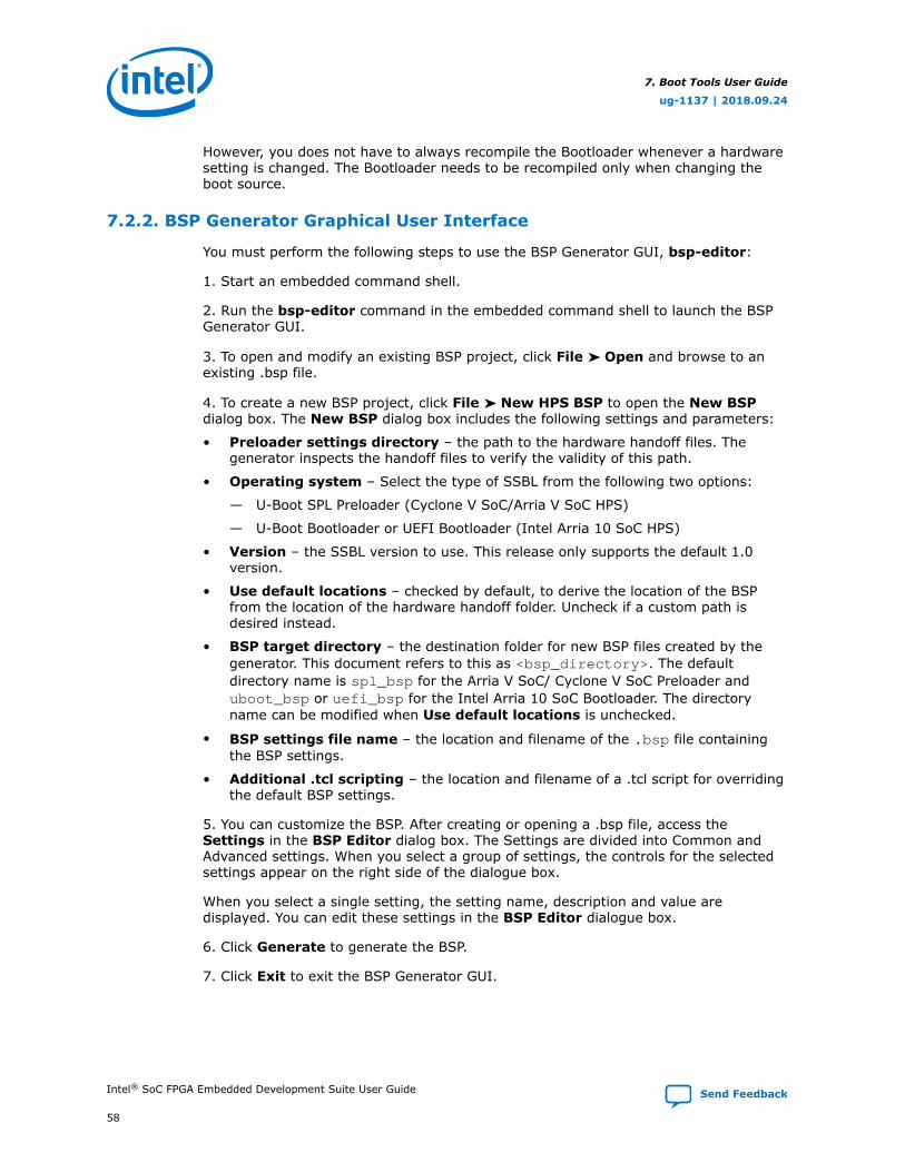
7.2.2. BSP Generator Graphical User Interface
You must perform the following steps to use the BSP Generator GUI, bsp-editor:
1. Start an embedded command shell.
2. Run the bsp-editor command in the embedded command shell to launch the BSPGenerator GUI.
3. To open and modify an existing BSP project, click File ➤ Open and browse to anexisting .bsp file.
4. To create a new BSP project, click File ➤ New HPS BSP to open the New BSPdialog box. The New BSP dialog box includes the following settings and parameters:
• Preloader settings directory – the path to the hardware handoff files. Thegenerator inspects the handoff files to verify the validity of this path.
• Operating system – Select the type of SSBL from the following two options:
— U-Boot SPL Preloader (Cyclone V SoC/Arria V SoC HPS)
— U-Boot Bootloader or UEFI Bootloader (Intel Arria 10 SoC HPS)
• Version – the SSBL version to use. This release only supports the default 1.0version.
• Use default locations – checked by default, to derive the location of the BSPfrom the location of the hardware handoff folder. Uncheck if a custom path isdesired instead.
• BSP target directory – the destination folder for new BSP files created by thegenerator. This document refers to this as <bsp_directory>. The defaultdirectory name is spl_bsp for the Arria V SoC/ Cyclone V SoC Preloader anduboot_bsp or uefi_bsp for the Intel Arria 10 SoC Bootloader. The directoryname can be modified when Use default locations is unchecked.
• BSP settings file name – the location and filename of the .bsp file containingthe BSP settings.
• Additional .tcl scripting – the location and filename of a .tcl script for overridingthe default BSP settings.
5. You can customize the BSP. After creating or opening a .bsp file, access theSettings in the BSP Editor dialog box. The Settings are divided into Common andAdvanced settings. When you select a group of settings, the controls for the selectedsettings appear on the right side of the dialogue box.
When you select a single setting, the setting name, description and value aredisplayed. You can edit these settings in the BSP Editor dialogue box.
6. Click Generate to generate the BSP.
7. Click Exit to exit the BSP Generator GUI.
7. Boot Tools User Guide
ug-1137 | 2018.09.24
Intel® SoC FPGA Embedded Development Suite User Guide Send Feedback
58

7.2.2.1. Using .tcl Scripts
Instead of using the default settings, you can create a tcl script file (.tcl) to definecustom settings during BSP creation.
set_setting is the only available .tcl command.
For more information about the list of available settings, refer to the "BSP Settings"section.
The following shows example commands that are used to set parameters in the BSPsettings file:
set_setting spl.boot.BOOT_FROM_QSPI trueset_setting spl.boot.QSPI_NEXT_BOOT_IMAGE 0x50000
Related Information
BSP Settings on page 62
7.2.3. BSP Generator Command Line Interface
The BSP command-line tools can be invoked from the embedded command shell, andprovide all the features available in the BSP Generator GUI:
• The bsp-create-settings tool creates a new BSP settings file.
• The bsp-update-settings tool updates an existing BSP settings file.
• The bsp-query-settings tool reports the setting values in an existing BSPsettings file.
• The bsp-generate-files tool generates a BSP from the BSP settings file.
Note: Help for each tool is available from the embedded command shell. To display help,type the following command:<name of tool> --help.
7.2.3.1. bsp-create-settings
The bsp-create-settings tool creates a new BSP settings file with default settings.You have the option to modify the BSP settings or generate the BSP files as shown inthe following example.
Example 1. Creating a New BSP Settings File
The following example creates a new Preloader BSP settings file, based on thehardware handoff information and using the default BSP settings:
bsp-create-settings --type spl -–bsp-dir . \ --settings settings.bsp \ --preloader-settings-dir ../../hps_isw_handoff/<hps_entity_name>
7. Boot Tools User Guide
ug-1137 | 2018.09.24
Send Feedback Intel® SoC FPGA Embedded Development Suite User Guide
59
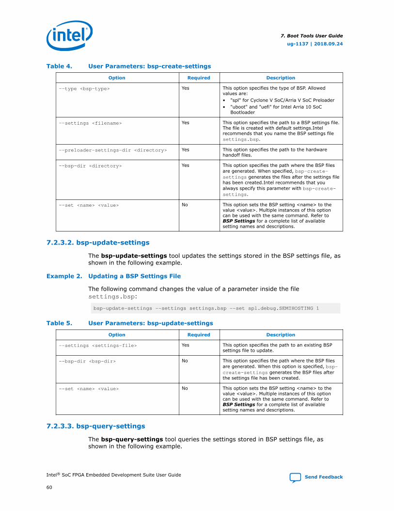
Table 4. User Parameters: bsp-create-settings
Option Required Description
--type <bsp-type> Yes This option specifies the type of BSP. Allowedvalues are:• "spl" for Cyclone V SoC/Arria V SoC Preloader• "uboot" and "uefi" for Intel Arria 10 SoC
Bootloader
--settings <filename> Yes This option specifies the path to a BSP settings file.The file is created with default settings.Intelrecommends that you name the BSP settings filesettings.bsp.
--preloader-settings-dir <directory> Yes This option specifies the path to the hardwarehandoff files.
--bsp-dir <directory> Yes This option specifies the path where the BSP filesare generated. When specified, bsp-create-settings generates the files after the settings filehas been created.Intel recommends that youalways specify this parameter with bsp-create-settings.
--set <name> <value> No This option sets the BSP setting <name> to thevalue <value>. Multiple instances of this optioncan be used with the same command. Refer toBSP Settings for a complete list of availablesetting names and descriptions.
7.2.3.2. bsp-update-settings
The bsp-update-settings tool updates the settings stored in the BSP settings file, asshown in the following example.
Example 2. Updating a BSP Settings File
The following command changes the value of a parameter inside the filesettings.bsp:
bsp-update-settings --settings settings.bsp --set spl.debug.SEMIHOSTING 1
Table 5. User Parameters: bsp-update-settings
Option Required Description
--settings <settings-file> Yes This option specifies the path to an existing BSPsettings file to update.
--bsp-dir <bsp-dir> No This option specifies the path where the BSP filesare generated. When this option is specified, bsp-create-settings generates the BSP files afterthe settings file has been created.
--set <name> <value> No This option sets the BSP setting <name> to thevalue <value>. Multiple instances of this optioncan be used with the same command. Refer toBSP Settings for a complete list of availablesetting names and descriptions.
7.2.3.3. bsp-query-settings
The bsp-query-settings tool queries the settings stored in BSP settings file, asshown in the following example.
7. Boot Tools User Guide
ug-1137 | 2018.09.24
Intel® SoC FPGA Embedded Development Suite User Guide Send Feedback
60

Example 3. Querying a BSP Settings File
The following command will retrieve all the settings from settings.bsp and displaysthe setting names and values:
bsp-query-settings --settings settings.bsp --get-all --show-names
Table 6. User Parameters: bsp-query-settings
Option Required Description
--settings <settings-file> Yes This option specifies the path to an existing BSPsettings file.
--get <name> No This option instructs bsp-query-settings toreturn the value of the BSP setting <name>.
--get-all No This option shows all the BSP settings values.When using --get-all,you must also use --show-names.
--show-names No This option only takes effect when used togetherwith --get <name> or --get-all. When usedwith one of these options, names and values of theBSP settings are shown side- by-side.
7.2.3.4. bsp-generate-files
The bsp-generate-files tool generates the files and settings stored in BSP settingsfile, as shown in the following examples.
Example 4. Generating Files After BSP Creation
The following commands create a settings file based on the handoff folder, and thengenerate the BSP files based on those settings:
bsp-create-settings --type spl --bsp-dir . \ --settings settings.bsp \ --preloader-settings-dir \ ../../hps_isw_handoff/<hps_entity_name>bsp-generate-files --settings settings.bsp --bsp-dir
Example 5. Generating Files After BSP Updates
The following commands update the settings of a an existing BSP settings file, andthen generate the BSP files based on those settings:
bsp-update-settings --settings settings.bsp --set \ spl.debug.SEMIHOSTING 1bsp-generate-files --settings settings.bsp --bsp-dir
Use the bsp-generate-files tool when BSP files need to be regenerated in one of thefollowing conditions:
• bsp-create-settings created the BSP settings, but the --bsp-dir parameter wasnot specified, so BSP files were not generated.
• bsp-update-settings updated the BSP settings, but the --bsp-dir parameter wasnot specified, so the files were not updated.
• You want to ensure the BSP files are up-to-date.
7. Boot Tools User Guide
ug-1137 | 2018.09.24
Send Feedback Intel® SoC FPGA Embedded Development Suite User Guide
61

Table 7. User Parameters: bsp-generate-files
Option Required Description
--settings <settings-file> Yes This option specifies the path to an existing BSPsettings file.
--bsp-dir <bsp-dir> Yes This option specifies the path where the BSP filesare generated.
7.2.4. BSP Files and Folders
The files and folders created with the BSP Generator are stored in the location youspecified in BSP target directory in the New BSP dialog box.
For Cyclone V SoC/Arria Preloader BSPs, the generated files include the following:
• settings.bsp – file containing all BSP settings
• Makefile – makefile used to compile the Preloader and create the preloaderimage; for more information, refer to Preloader Compilation
• preloader.ds – Arm DS-5 Intel SoC FPGA Edition script, that can be used todownload and debug the Preloader on a target device
• generated – folder containing files generated from the hardware handoff files
For Intel Arria 10 SoC Bootloader BSPs, for both U-Boot and UEFI, the generated filesinclude the following:
• settings.bsp – file containing all BSP settings
• Makefile – makefile used to compile the Bootloader, convert the Bootloaderdevice tree file to binary, and create the combined Bootloader and BootloaderDevice Tree image; for more information, refer to Preloader Compilation
• config.mk – makefile configuration file, containing the boot source selection andwhether the Bootloader compilation is selected
• devicetree.dts – Bootloader device tree, containing the Bootloader customizationdetails, derived from the handoff files and you settings
7.2.5. BSP Settings
This section lists all the available BSP settings, which can be accessed from either theGraphical User Interface application (bsp-editor) or from the command line tools(bsp-create-settings, bsp-update-settings, bsp-query-settings).
The available BSP settings are different between Cyclone V SoC and Arria V SoC SSBL(Preloader) and Intel Arria 10 SoC SSBL (Bootloader).
7.2.5.1. Cyclone V SoC and Arria V SoC BSP Settings
Table 8. Cyclone V SoC and Arria V SoC BSP Settings
BSP Setting Type Default Value Description
spl.PRELOADER_TGZ String <SoC EDSinstallationdirectory>/host_tools/altera/
This setting specifies the path to archivefile containing the preloader source files.
continued...
7. Boot Tools User Guide
ug-1137 | 2018.09.24
Intel® SoC FPGA Embedded Development Suite User Guide Send Feedback
62

BSP Setting Type Default Value Description
preloader/uboot-socfpga.tar.gz"
spl.CROSS_COMPILE String "arm-altera-eabi-"
This setting specifies the crosscompilation tool chain for use.
spl.boot.BOOT_FROM_QSPI Boolean False Select the source for the subsequentboot image. Note that only one sourcecan be active at a time. When using bsp-create-settings or bsp-update-settings, you must turn off the bootoption that is currently turned on beforeyou can turn on a different boot option.
spl.boot.BOOT_FROM_SDMMC Boolean True
spl.boot.BOOT_FROM_RAM Boolean False
spl.boot.BOOT_FROM_NAND Boolean False
spl.boot.QSPI_NEXT_BOOT_IMAGE Hexadecimal 0x60000 This setting specifies the location of thesubsequent boot image in QSPI.
spl.boot.SDMMC_NEXT_BOOT_IMAGE Hexadecimal 0x40000 This setting specifies the location of thesubsequent boot image in SD/MMC.
spl.boot.NAND_NEXT_BOOT_IMAGE Hexadecimal 0xC0000 This setting specifies the location of thesubsequent boot image in NAND.
spl.boot.FAT_SUPPORT Boolean False Enable FAT partition support whenbooting from SD/MMC.
spl.boot.FAT_BOOT_PARTITION DecimalNumber 1 When FAT partition support is enabled,this specifies the FAT partition where theboot image is located.
spl.boot.FAT_LOAD_PAYLOAD_NAME String "u-boot.img" When FAT partition supported is enabled,this specifies the boot image filename tobe used.
spl.boot.WATCHDOG_ENABLE Boolean True This setting enables the watchdog duringthe preloader execution phase. Thewatchdog remains enabled after thepreloader exits.
spl.boot.CHECKSUM_NEXT_IMAGE Boolean True This setting enables the preloader tovalidate the checksum in the subsequentboot image header information.
spl.boot.EXE_ON_FPGA Boolean False This setting executes the preloader onthe FPGA. Selectspl.boot.EXE_ON_FPGA when thepreloader is configured to boot from theFPGA.
spl.boot.STATE_REG_ENABLE Boolean True This setting enables writing the magicvalue to the INITSWSTATE register inthe system manager when the preloaderexists; this indicates to the BootROMthat the preloader has run successfully.
spl.boot.BOOTROM_HANDSHAKE_CFGIO
Boolean True This setting enables handshake withBootROM when configuring the IOCSRand pin multiplexing. Ifspl.boot.BOOTROM_HANDSHAKE_CFGIO is enabled and warm reset occurswhen the preloader is configuring IOCSRand pin multiplexing, the BootROM willreconfigure IOCSR and pin multiplexingagain. This option is enabled by default.
spl.boot.WARMRST_SKIP_CFGIO Boolean True This setting enables the preloader to skipIOCSR and pin multiplexing configurationduring warm reset.
continued...
7. Boot Tools User Guide
ug-1137 | 2018.09.24
Send Feedback Intel® SoC FPGA Embedded Development Suite User Guide
63

BSP Setting Type Default Value Description
spl.boot.WARMRST_SKIP_CFGIO isonly applicable if the boot ROM hasskipped IOCSR and pin multiplexingconfiguration.
spl.boot.SDRAM_INITIALIZATION Boolean False Initialize the SDRAM to initialize the ECCbits.
spl.boot.SDRAM_ECC_INIT_BOOT_REGION_START
Hexadecimal 0x1000000 The start address of the memory regionwithin the SDRAM to be initialized.
spl.boot.SDRAM_ECC_INIT_BOOT_REGION_END
Hexadecimal 0x2000000 The end address of the memory regionwithin SDRAM to be initialized.
spl.boot.SDRAM_ECC_INIT_REMAIN_REGION
Boolean True Initialize the remaining SDRAM, duringthe flash accesses to load the image.
spl.debug.DEBUG_MEMORY_WRITE Boolean False This setting enables the preloader towrite debug information to memory fordebugging, useful when UART is notavailable. The address is specified byspl.debug.DEBUG_ MEMORY_ADDR.
spl.debug.SEMIHOSTING Boolean False This setting enables semihosting supportin the preloader, for use with a debuggertool. spl.debug.SEMIHOSTING isuseful when UART is unavailable.
spl.debug.SKIP_SDRAM Boolean False The preloader skips SDRAM initializationand calibration when this setting isenabled.
spl.performance.SERIAL_SUPPORT Boolean True This setting enables UART print outsupport, enabling preloader code to callprintf() at runtime with debugginginformation. stdout output from printf()is directed to the UART. You can view thisdebugging information by connecting aterminal program to the UART specifiedperipheral.
spl.reset_assert.DMA Boolean False When enabled, this setting will force thecorresponding peripheral to remain inreset. You must ensure the debuggerdoes not read registers from thesecomponents.
spl.reset_assert.GPIO0 Boolean False
spl.reset_assert.GPIO1 Boolean False
spl.reset_assert.GPIO2 Boolean False
spl.reset_assert.L4WD1 Boolean False
spl.reset_assert.OSC1TIMER1 Boolean False
spl.reset_assert.SDR Boolean False
spl.reset_assert.SPTIMER0 Boolean False
spl.reset_assert.SPTIMER1 Boolean False
spl.warm_reset_handshake.FPGA Boolean True This setting enables the reset managerto perform handshake with the FPGAbefore asserting a warm reset.
spl.warm_reset_handshake.ETR Boolean True This setting enables the reset managerto request that the Embedded TraceRouter (ETR) stalls the AdvancedeXtensible Interface (AXI) master andwaits for the ETR to finish any
continued...
7. Boot Tools User Guide
ug-1137 | 2018.09.24
Intel® SoC FPGA Embedded Development Suite User Guide Send Feedback
64

BSP Setting Type Default Value Description
outstanding AXI transactions beforeasserting a warm reset of the L3interconnect or a debug reset of the ETR.
spl.warm_reset_handshake.SDRAM Boolean False This option allows the SDRAM contentsto be preserved across warm resets.Note: When using this option, the
SDRAM controller is notcompletely re-initialized whencoming back from warm reset.This may be a problem wheneverthe warm reset is generated bythe Watchdog as a consequenceof an SDRAM controller failure.
Note: Also the SDRAM PLL is not re-initialized when this option isenabled and the system comesout of the warm reset.
spl.boot.FPGA_MAX_SIZE Hexadecimal 0x10000 This setting specifies the maximum code(.text and .rodata) size that can fitwithin the FPGA. If the code build isbigger than the specified size, a builderror is triggered.
spl.boot.FPGA_DATA_BASE Hexadecimal 0xFFFF0000 This setting specifies the base locationfor the data region (.data, .bss, heapand stack) when execute on FPGA isenabled.
spl.boot.FPGA_DATA_MAX_SIZE Hexadecimal 0x10000 This setting specifies the maximum data(.data, .bss, heap and stack) size thatcan fit within FPGA. If the code build isbigger than the specified size, a builderror is triggered.
spl.debug.DEBUG_MEMORY_ADDR Hexadecimal 0xFFFFFD00 This setting specifies the base addressfor storing preloader debug informationenabled with thespl.debug.DEBUG_MEMORY_ WRITEsetting.
spl.debug.DEBUG_MEMORY_SIZE Hexadecimal 0x200 This setting specifies the maximum sizeused for storing preloader debuginformation.
continued...
7. Boot Tools User Guide
ug-1137 | 2018.09.24
Send Feedback Intel® SoC FPGA Embedded Development Suite User Guide
65

BSP Setting Type Default Value Description
spl.debug.DEBUG_MEMORY_ADDR Hexadecimal 0xFFFFFD00 This setting specifies the base addressfor storing preloader debug informationenabled with thespl.debug.DEBUG_MEMORY_ WRITEsetting.
spl.debug.HARDWARE_DIAGNOSTIC Boolean False Enable hardware diagnostic support. Toenable this, at least 1GB of memory isneeded, otherwise hardware diagnosticwill fail to run properly.
spl.boot.RAMBOOT_PLLRESET Boolean True Execute RAM Boot PLL reset code onwarm reset when CSEL = 00. This optionis required to enable correct warm resetfunctionality when using CSEL = 00.When enabling this option, the upper 4KB of OCRAM are reserved and must notbe modified by you software.Note: Enabling this feature with CSEL !
= 00 does not have any effect, asthe impacted code checks forthis.
7.2.5.2. Intel Arria 10 SoC BSP Settings
The Intel Arria 10 SoC BSP Settings are divided in four different groups:
• Main Group
• MPU Firewall
• L3 Firewall Group
• F2S Firewall Group
The following table presents the settings prefix to be added in front of the settingname for each of the groups. They are presented in a table to make the rest of thissection more readable.
Table 9. Intel Arria 10 SoC BSP Firewall Setting Prefixes
Settings Group Setting Group Prefix
Main Group N/A
MPU Firewall For U-Boot:altera_arria10_soc_noc_arria10_uboot_driver.I_NOC.mpu_m0.noc_fw_ddr_mpu_fpga2sdram_ddr_scr.For UEFI:altera_arria10_soc_noc_arria10_uefi_driver.I_NOC.mpu_m0.noc_fw_ddr_mpu_fpga2sdram_ddr_scr.
L3 Firewall Group For U-Boot:altera_arria10_soc_noc_arria10_uboot_driver.I_NOC.mpu_m0.noc_fw_ddr_l3_ddr_scr.For UEFI:altera_arria10_soc_noc_arria10_uefi_driver.I_NOC.mpu_m0.noc_fw_ddr_l3_ddr_scr.
F2S Firewall Group For U-Boot:altera_arria10_soc_noc_arria10_uboot_driver.I_NOC.mpu_m0.noc_fw_ddr_mpu_fpga2sdram_ddr_scr.For UEFI:altera_arria10_soc_noc_arria10_uefi_driver.I_NOC.mpu_m0.noc_fw_ddr_mpu_fpga2sdram_ddr_scr.
7. Boot Tools User Guide
ug-1137 | 2018.09.24
Intel® SoC FPGA Embedded Development Suite User Guide Send Feedback
66

7.2.5.2.1. Intel Arria 10 SoC Main BSP Settings Group
Table 10. Intel Arria 10 SoC Main BSP Settings Group for U-Boot
BSP Setting Type Default Value Description
uboot.boot_device String SD/MMC Select the source for the boot image.Possible values are SD/MMC, QSPI, andNAND.
uboot.model String SOCFPGAArria10 Dev Kit
Name of the board to be displayed whenbootloader starts.
uboot.external_fpga_config Boolean False Configure Uboot to wait early on in theboot sequence to allow the FPGA to bebrought to user mode by either a JTAGdownload or an externally connectedflash.
uboot.rbf_filename String socfpga.rbf Full FPGA .rbf filename. This setting isignored when theuboot.external_fpga_configsetting is enabled.
uboot.rbf_offset Hexadecimal 0x720000 RBF offset address in QSPI Flash.
uboot.disable_uboot_build Boolean False Can be used to disable building Uboot,and just generate the Bootloader DeviceTree file.
uboot.secureboot.enable_bootloader_encryption
Boolean 0 Encrypt Bootloader using key filespecified.
uboot.secureboot.enable_bootloader_signing
Boolean 0 Sign Bootloader using the key pair filespecified.
uboot.secureboot.encryption_key_file
String encrypt.key Key file used for Bootloader encryption.
uboot.secureboot.encryption_key_name
String key1 Key Name to use within Key File forBootloader Encryption.
uboot.secureboot.signing_key_fpga_offset
Hexadecimal 0x0 Offset from H2F Bridge Base Address(0xC0000000) to location of root-public-key.
uboot.secureboot.signing_key_pair_file
String root_key.pem Key Pair File to use when signing isenabled. You can generate this file withthe command: 'make generate-signing-key-pair-file'.
uboot.secureboot.signing_key_type
String user Sign Bootloader using key pair filespecified.
Table 11. Intel Arria 10 SoC Main BSP Settings Group for UEFI
BSP Setting Type Default Value Description
uefi.boot_device String SD/MMC Select the source for the boot image.Possible values are SD/MMC, QSPI, andNAND.
uefi.model String SOCFPGAArria10 Dev Kit
Name of the board to be displayed whenbootloader starts.
continued...
7. Boot Tools User Guide
ug-1137 | 2018.09.24
Send Feedback Intel® SoC FPGA Embedded Development Suite User Guide
67

BSP Setting Type Default Value Description
uefi.external_fpga_config Boolean False Configure UEFI to wait early on in theboot sequence to allow the FPGA to bebrought to user mode by either a JTAGdownload or an externally connectedflash.
uefi.rbf_filename String socfpga.rbf Full FPGA .rbf filename. This setting isignored when theuefi.external_fpga_config settingis enabled.
uefi.rbf_offset Hexadecimal 0x720000 RBF offset address in QSPI Flash.
uefi.disable_uefi_build Boolean False Can be used to disable building UEFI,and just generate the Bootloader DeviceTree file.
For more information about authentication and encryption, refer to the Intel Arria 10SoC Secure Boot User Guide.
Related Information
Arria 10 SoC Secure Boot User GuideFor more information about authentication and encryption
7.2.5.2.2. Intel Arria 10 SoC Bootloader MPU Firewall BSP Settings Group
Table 12. Intel Arria 10 SoC Bootloader MPU Firewall BSP Settings Group
BSP Setting(1) Type Default Value Description
enable.mpuregion0enable Boolean True Enable MPU Firewall Regions
enable.mpuregion1enable False
enable.mpuregion2enable False
enable.mpuregion3enable False
mpuregion0addr.base Hexadecimal 0x0 MPU Firewall region bases
mpuregion1addr.base
mpuregion2addr.base
mpuregion3addr.base
mpuregion0addr.limit Hexadecimal 0xFFFF MPU Firewall region limits
mpuregion1addr.limit
mpuregion2addr.limit
mpuregion3addr.limit
(1) Use the Intel Arria 10 SoC BSP Firewall Setting Prefixes. Table 9 on page 66
7. Boot Tools User Guide
ug-1137 | 2018.09.24
Intel® SoC FPGA Embedded Development Suite User Guide Send Feedback
68
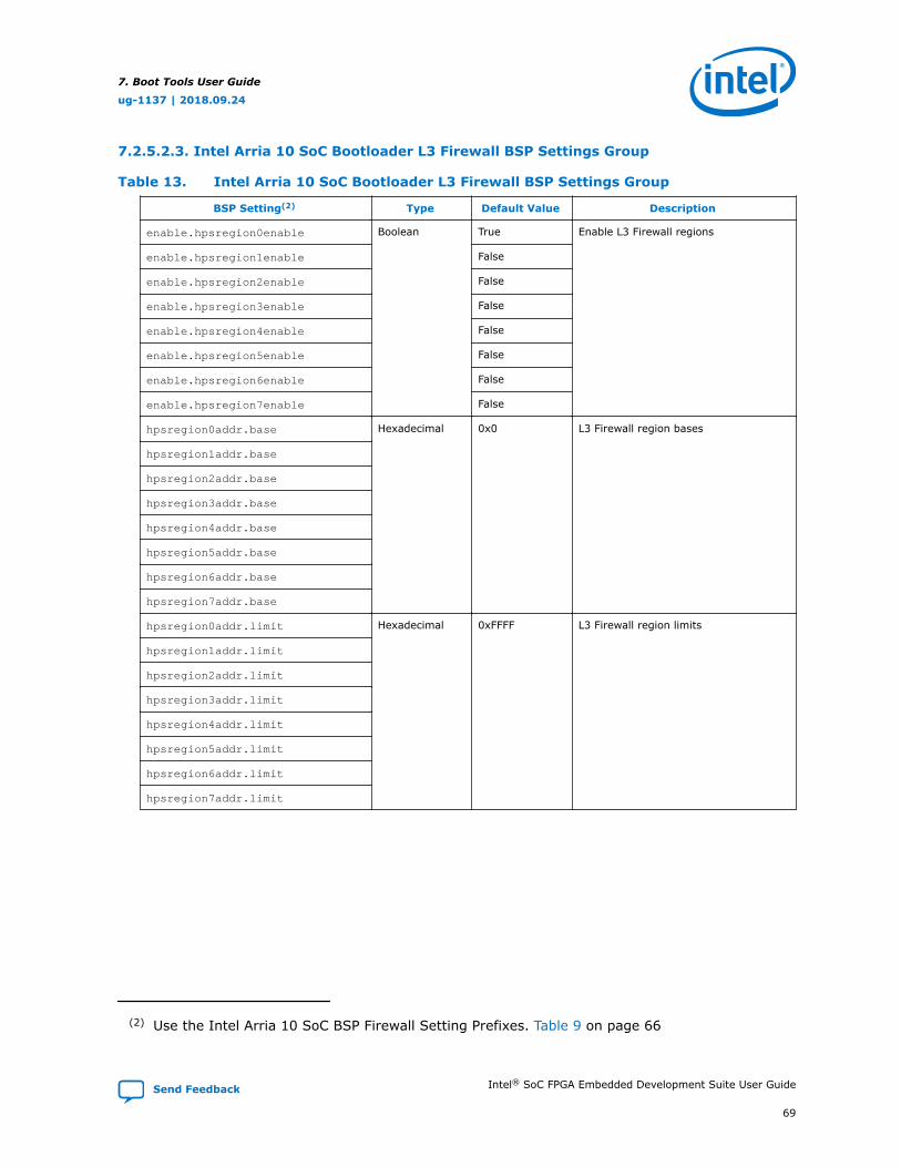
7.2.5.2.3. Intel Arria 10 SoC Bootloader L3 Firewall BSP Settings Group
Table 13. Intel Arria 10 SoC Bootloader L3 Firewall BSP Settings Group
BSP Setting(2) Type Default Value Description
enable.hpsregion0enable Boolean True Enable L3 Firewall regions
enable.hpsregion1enable False
enable.hpsregion2enable False
enable.hpsregion3enable False
enable.hpsregion4enable False
enable.hpsregion5enable False
enable.hpsregion6enable False
enable.hpsregion7enable False
hpsregion0addr.base Hexadecimal 0x0 L3 Firewall region bases
hpsregion1addr.base
hpsregion2addr.base
hpsregion3addr.base
hpsregion4addr.base
hpsregion5addr.base
hpsregion6addr.base
hpsregion7addr.base
hpsregion0addr.limit Hexadecimal 0xFFFF L3 Firewall region limits
hpsregion1addr.limit
hpsregion2addr.limit
hpsregion3addr.limit
hpsregion4addr.limit
hpsregion5addr.limit
hpsregion6addr.limit
hpsregion7addr.limit
(2) Use the Intel Arria 10 SoC BSP Firewall Setting Prefixes. Table 9 on page 66
7. Boot Tools User Guide
ug-1137 | 2018.09.24
Send Feedback Intel® SoC FPGA Embedded Development Suite User Guide
69

7.2.5.2.4. Intel Arria 10 SoC Bootloader FPGA-to-SDRAM Firewall BSP Settings Group
Table 14. Intel Arria 10 SoC Bootloader FPGA-to-SDRAM Firewall BSP Settings Group
BSP Setting(3) Type Default Value Description
enable.fpga2sdram0region0 Boolean True Enable FPGA-to-SDRAM Firewallregions
enable.fpga2sdram0region1 True
enable.fpga2sdram0region2 True
enable.fpga2sdram0region3 False
enable.fpga2sdram1region0 False
enable.fpga2sdram1region1 False
enable.fpga2sdram1region2 False
enable.fpga2sdram1region3 False
enable.fpga2sdram2region0 False
enable.fpga2sdram2region1 False
enable.fpga2sdram2region2 False
enable.fpga2sdram2region3 False
fpga2sdram0region0addr.base Hexadecimal 0x0 FPGA-to-SDRAM Firewall region bases
fpga2sdram0region1addr.base
fpga2sdram0region2addr.base
fpga2sdram0region3addr.base
fpga2sdram1region0addr.base
fpga2sdram1region1addr.base
fpga2sdram1region2addr.base
fpga2sdram1region3addr.base
fpga2sdram2region0addr.base
fpga2sdram2region1addr.base
fpga2sdram2region2addr.base
fpga2sdram2region3addr.base
fpga2sdram0region0addr.limit Hexadecimal 0xFFFF FPGA-to-SDRAM Firewall region limits
fpga2sdram0region1addr.limit
fpga2sdram0region2addr.limit
fpga2sdram0region3addr.limit
fpga2sdram1region0addr.limit
fpga2sdram1region1addr.limit
continued...
(3) Use the Intel Arria 10 SoC BSP Firewall Setting Prefixes. Table 9 on page 66
7. Boot Tools User Guide
ug-1137 | 2018.09.24
Intel® SoC FPGA Embedded Development Suite User Guide Send Feedback
70

BSP Setting(3) Type Default Value Description
fpga2sdram1region2addr.limit
fpga2sdram1region3addr.limit
fpga2sdram2region0addr.limit
fpga2sdram2region1addr.limit
fpga2sdram2region2addr.limit
fpga2sdram2region3addr.limit
7.3. Bootloader Image Tool (mkpimage)
The Bootloader Image Tool (mkpimage) creates an Intel BootROM-compatible imageof the Arria V SoC and Cyclone V SoC Preloader or Intel Arria 10 SoC Bootloader. Thetool can also decode the header of previously generated images.
The mkpimage tool makes the following assumptions:
• The input file format is raw binary. You must use the objcopy utility provided withthe GNU Compiler Collection (GCC) tool chain from the Mentor Graphics website toconvert other file formats, such as Executable and Linking Format File (.elf),Hexadecimal (Intel-Format) File (.hex), or S-Record File (. srec), to a binaryformat.
• The output file format is binary.
• The tool always creates the output image at the beginning of the binary file. If theimage must be programmed at a specific base address, you must supply theaddress information to the flash programming tool.
• The output file contains only Preloader or Bootloader images. Other images suchas Linux, SRAM Object File (.sof) and user data are programmed separately usinga flash programming tool or related utilities in the U-boot on the target system.
Figure 49. Basic Operation of the mkpimage Tool
SSBL
(empty)Exception Vector
CRC Checksum
HeaderSSBL
Exception Vector
CRC Checksum
Header
Padding
+
7.3.1. Operation
The mkpimage tool runs on a host machine. The tool generates the header and CRCchecksum and inserts them into the output image with the bootloader program imageand its exception vector.
For certain flash memory tools, the position of the bootloader images must be alignedto a specific block size; the mkpimage tool generates any padding data that may berequired.
(3) Use the Intel Arria 10 SoC BSP Firewall Setting Prefixes. Table 9 on page 66
7. Boot Tools User Guide
ug-1137 | 2018.09.24
Send Feedback Intel® SoC FPGA Embedded Development Suite User Guide
71

The mkpimage tool optionally decodes and validates header information when given apre-generated bootloader image.
As illustrated, the binary bootloader image is an input to the mkpimage tool. Thecompiler leaves an empty space between the bootloader exception vector and theprogram. The mkpimage tool overwrites this empty region with header informationand calculates a checksum for the whole image.
When necessary, the mkpimage tool appends the padding data to the output image.
The mkpimage tool can operate with either one or four input files. Operation on fourinput files consists in processing each file individually, then concatenating the fourresulted images.
7.3.2. Header File Format
The mkpimage header file format has two versions:
• Version 0, used for Cyclone V SoC and Arria V SoC FSBL (Preloader)
• Version 1, used for Intel Arria 10 SoC Bootloader
For Version 0, used for Cyclone V SoC and Arria V SoC Preloader, the header includesthe following:
• Validation word (0x31305341)
• Version field (set to 0x0)
• Flags field (set to 0x0)
• Program length measured by the number of 32 bit words in the Preloader program
• 16-bit checksum of the header contents (0x40 – 0x49)
Figure 50. Header Format Version 0
Validation word (0x31305341)0x40
Version0x44Flags0x45Program length in 32-bit words0x46Reserved (0x0)0x48Header Checksum0x4A
For Version 1, used for Intel Arria 10 SoC Bootloader, the header includes thefollowing:
• Validation word (0x31305341).
• Version field (set to 0x1).
• Flags field (set to 0x0).
• Header length, in bytes, set to 0x14 (20 bytes).
7. Boot Tools User Guide
ug-1137 | 2018.09.24
Intel® SoC FPGA Embedded Development Suite User Guide Send Feedback
72

• Total program length (including the exception vectors and the CRC field) in bytes.For an image to be valid, length must be a minimum of 0x5C (92 bytes) and amaximum of 0x32000 (200KiB).
• Program entry offset relative to the start of header (0x40) and should be 32-bitword-aligned. Default is 0x14, any value smaller than that is invalid.
• 16-bit checksum of the header contents (0x40 – 0x51):
Figure 51. Header Format Version 1
Validation word (0x31305341)0x40
Version0x44Flags0x45
Program entry offset0x4CReserved (0x0)0x50Header Checksum0x52
Header length in bytes0x46Program length in bytes0x48
The header checksum for both versions of the mkpimage header is the CRC checksumof the byte value from offset 0x0 to (n*4)-4 bytes where n is the program length.
The CRC is a standard CRC32 with the polynomial:
x32 + x26 + x23 + x22 + x16 + x12 + x11 + x10 + x8 + x7 + x5 + x4 + x2 + x + 1
There is no reflection of the bits and the initial value of the remainder is 0xFFFFFFFFand the final value is exclusive OR-ed with 0xFFFFFFFF.
7.3.3. Tool Usage
The mkimage tool has three usage models:
• Single image creation
• Quad image creation
• Single or quad image decoding
If an error is found during the make image process, the tool stops and reports theerror. Possible error conditions include:
• For Cyclone V SoC and Arria V SoC Preloaders: input image is smaller than 81bytes or larger than 60 KB.
• For Intel Arria 10 SoC Bootloaders: input image is smaller than 92 bytes or largerthan 200 KB.
Type mkpimage to launch the tool. The --help option provides a tool description andtool usage and option information.
$ mkpimage --helpmkpimage version 18.0
Description: This tool creates an Intel BootROM-compatible image of SecondStage Boot Loader (SSBL). The input and output files are in binary format.It can also decode and check the validity of previously generated image.
Usage: Create quad image: mkpimage [options] -hv <num> -o <outfile> <infile> <infile> <infile> <infile>
7. Boot Tools User Guide
ug-1137 | 2018.09.24
Send Feedback Intel® SoC FPGA Embedded Development Suite User Guide
73

Create single image: mkpimage [options] -hv <num> -o <outfile> <infile> Decode single/quad image: mkpimage -d [-a <num>] <infile>
Options: -a (--alignment) <num> : Address alignment in kilobytes for output image (64, 128, 256, etc.), default to 64 for header version 0 and 256 for header version 1, override if the NAND flash has a different block size. If outputting a single image, value of '0' is permitted to specify no flash block padding (needed for SSBL image encryption). -d (--decode) : Flag to decode the header information from input file and display it -f (--force) : Flag to force decoding even if the input file is an unpadded image -h (--help) : Display this help message and exit -hv (--header-version) <num> : Header version to be created (Arria/Cyclone V SoC = 0, Intel Arria 10 SoC = 1) -o (--output) <outfile> : Output file, relative and absolute path supported -off (--offset) <num> : Program entry offset relative to start of header (0x40), default to 0x14. Used for header version 1 only -v (--version) : Display version and exit
7.3.4. Output Image Layout
7.3.4.1. Base Address
The bootable SSBL image must be placed at 0x0 for NAND and QSPI flash. ForSD/MMC the image can also be placed at 0x0, but typically the image is placed atoffset 0x0 in a custom partition of type 0xA2. The custom partition does not have afilesystem on it. The BootROM is able to locate the partition using the MBR (MasterBoot Record) located at 0x0 on the SD/MMC card.
The mkpimage tool always places the output image at the start of the output binaryfile, regardless of the target flash memory type. The flash programming tool isresponsible for placing the image at the desired location on the flash memory device.
7.3.4.2. Size
For Cyclone V SoC and Arria V SoC, a single Preloader has a maximum 60 KB imagesize. You can store up to four preloader images in flash. If the BootROM does not finda valid preloader image at the first location, it attempts to read an image from thenext location and so on. To take advantage of this feature, program four preloaderimages in flash.
For Intel Arria 10 SoC, a single Bootloader has a maximum 200 KB image size. Youcan store up to four Bootloader images in flash. If the BootROM does not find a validBootloader image at the first location, it attempts to read the next one and so on. Totake advantage of this feature, program four Bootloader images in flash.
7. Boot Tools User Guide
ug-1137 | 2018.09.24
Intel® SoC FPGA Embedded Development Suite User Guide Send Feedback
74

7.3.4.3. Address Alignment
For Cyclone V SoC and Arria V SoC, every Preloader image has to be aligned to a64KB boundary, except for NAND devices. For NAND devices, each Preloader imagehas to be aligned to the greater of 64 KB or NAND block size.
For Intel Arria 10 SoC, every Bootloader image has to be aligned to a 256 KBboundary, except for NAND devices. For NAND devices, each Bootloader image has tobe aligned to the greater of 256 KB or NAND block size.
The following tables present typical image layouts, that are used for QSPI, SD/MMCand NAND devices with NAND erase block size equal or less to 64 KB (for Cyclone VSoC/Arria V SoC) or 256 KB (for Intel Arria 10 SoC).
Table 15. Typical Arria V SoC/Cyclone V SoC Preloader Image Layout
Offset Image
0x30000 Preloader Image 3
0x20000 Preloader Image 2
0x10000 Preloader Image 1
0x00000 Preloader Image 0
Table 16. Typical Intel Arria 10 SoC Bootloader Image Layout
Offset Image
0xC0000 Bootloader Image 3
0x80000 Bootloader Image 2
0x40000 Bootloader Image 1
0x00000 Bootloader Image 0
The mkpimage tool is unaware of the target flash memory type. If you do not specifythe block size, the default is 64 KB.
7.3.4.3.1. NAND Flash
Each Preloader or Bootloader image occupies an integer number of blocks. A block isthe smallest entity that can be erased, so updates to a particular boot image do notimpact the other images.
For example for Cyclone V SoC and Arria V SoC, a single Preloader image has amaximum size of 64 KB. But it the NAND block is 128 KB, then the Preloader imageswill need to be located at 128 KB intervals.
7.3.4.3.2. Serial NOR Flash
Each QSPI boot image occupies an integer number of sectors unless subsector erase issupported; this ensures that updating one image does not affect other images.
7. Boot Tools User Guide
ug-1137 | 2018.09.24
Send Feedback Intel® SoC FPGA Embedded Development Suite User Guide
75

7.3.4.3.3. SD/MMC
The master boot record, located at the first 512 bytes of the device memory, containspartition address and size information. The Preloader and Bootloader images arestored in partitions of type 0xA2. Other items may be stored in other partition typesaccording to the target file system format.
You can use the fdisk tool to set up and manage the master boot record. When thefdisk tool partitions an SD/MMC device, the tool creates the master boot record at thefirst sector, with partition address and size information for each partition on the SD/MMC.
7.3.4.4. Padding
The mkimage tool inserts a CRC checksum in the unused region of the image. Paddingfills the remaining unused regions. The contents of the padded and unused regions ofthe image are undefined.
Related Information
• Arria V Hard Processor System Technical Reference ManualFor more information, please refer to the Booting and Configuration chapter.
• Cyclone V Hard Processor System Technical Reference ManualFor more information, please refer to the Booting and Configuration chapter.
• Arria 10 Hard Processor System Technical Reference ManualFor more information, please refer to the Booting and Configuration chapter.
7.4. U-Boot Image Tool (mkimage)
Both the FSBL and SSBL require the presence of the U-Boot image header at thebeginning of the next stage boot image. Depending on usage scenario, other itemsthat are loaded by either Preloader or Bootloader may also require the presence of theU-Boot image header.
The mkimage utility is delivered with SoC EDS and can be used to append the U-Bootimage header to the next stage boot image or any other required files.
Figure 52. mkimage Header
mkimage Signature Header0x0000Input File0x0040
The header consists of the following items:
• Image magic number - determines if the image is a valid boot image
• Image data size - the length of the image to be copied
• Data load address - the entry point of the boot image (not used for items that arenot bootable images)
• Operating system - determines the type of image
• Image name - the name of the boot image
• Image CRC - the checksum value of the boot image
7. Boot Tools User Guide
ug-1137 | 2018.09.24
Intel® SoC FPGA Embedded Development Suite User Guide Send Feedback
76

Figure 53. mkimage Header Layout
Magic Number0x0000Data Load Address
Header CRC Timestamp Image Data SizeEntrypoint Image CRC O A T C
Image Name
0x00100x00200x00300x0040
0x4 0x8 0xC
O – Operating System A – Architecture T –Type C – Compression
7.4.1. Tool Options
mkimage invokes the mkimage tool and the --help option provides the tooldescription and option information.
$ mkimage --helpUsage: mkimage -l image -l ==> list image header information mkimage [-x] -A arch -O os -T type -C comp -a addr -e ep -n name -d data_file[:data_file...] image -A ==> set architecture to 'arch' -O ==> set operating system to 'os' -T ==> set image type to 'type' -C ==> set compression type 'comp' -a ==> set load address to 'addr' (hex) -e ==> set entry point to 'ep' (hex) -n ==> set image name to 'name' -d ==> use image data from 'datafile' -x ==> set XIP (execute in place) mkimage [-D dtc_options] [-f fit-image.its|-F] fit-image -D => set options for device tree compiler -f => input filename for FIT sourceSigning / verified boot not supported (CONFIG_FIT_SIGNATURE undefined) mkimage -V ==> print version information and exit
7.4.2. Usage Examples
Example 6. Creating a U-boot Image
mkimage –A arm –T firmware –C none –O u-boot –a 0x08000040 –e 0 –n "U-Boot 2014.10 for SOCFGPA board" –d u-boot.bin u-boot.img
Example 7. Creating a BareMetal Application Image
mkimage -A arm -O u-boot -T standalone -C none -a 0x02100000 -e 0 -n "baremetal image" -d hello_world.bin hello_world.img
7.5. Building the Bootloader
7.5.1. Building the Cyclone V SoC and Arria V SoC Preloader
The following figure presents the Cyclone V SoC and Arria V SoC Preloader build flow,as performed by the generated Makefile when invoking make. In order to keep theillustration simple, the generated Makefile itself is not shown.
7. Boot Tools User Guide
ug-1137 | 2018.09.24
Send Feedback Intel® SoC FPGA Embedded Development Suite User Guide
77
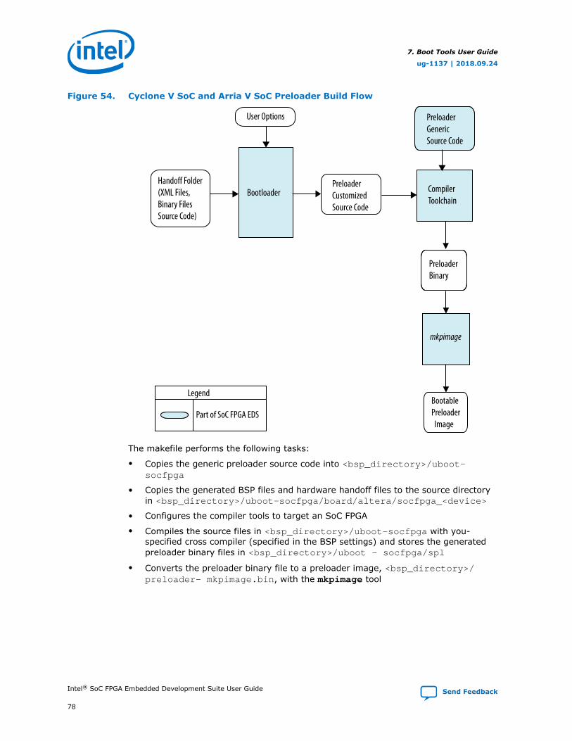
Figure 54. Cyclone V SoC and Arria V SoC Preloader Build Flow
Handoff Folder(XML Files,Binary FilesSource Code)
User Options
BootloaderPreloaderCustomizedSource Code
CompilerToolchain
PreloaderBinary
mkpimage
BootablePreloader Image
Legend
Part of SoC FPGA EDS
PreloaderGenericSource Code
The makefile performs the following tasks:
• Copies the generic preloader source code into <bsp_directory>/uboot-socfpga
• Copies the generated BSP files and hardware handoff files to the source directoryin <bsp_directory>/uboot-socfpga/board/altera/socfpga_<device>
• Configures the compiler tools to target an SoC FPGA
• Compiles the source files in <bsp_directory>/uboot-socfpga with you-specified cross compiler (specified in the BSP settings) and stores the generatedpreloader binary files in <bsp_directory>/uboot - socfpga/spl
• Converts the preloader binary file to a preloader image, <bsp_directory>/preloader- mkpimage.bin, with the mkpimage tool
7. Boot Tools User Guide
ug-1137 | 2018.09.24
Intel® SoC FPGA Embedded Development Suite User Guide Send Feedback
78

The makefile contains the following targets:
• make all – compiles the preloader
• make clean – deletes preloader-mkpimage.bin from the <bsp_directory>
• make clean-all – deletes <bsp_directory>, including the source files in thedirectory
7.5.2. Building the Intel Arria 10 SoC Bootloader
The following figure presents the Intel Arria 10 SoC Bootloader build flow, asperformed by the generated Makefile when invoking make. In order to keep theillustration simple, the generated Makefile itself is not shown.
Figure 55. Intel Arria 10 SoC Bootloader Build Flow
Bootloader
User Options
Handoff FolderXML (Files)
BootloaderDevice Tree
BootloaderSource Code
Compiler Toolchain
BootloaderBinary
Bootable Combined
Image
Device Tree Compiler
Bootloader Device Tree
Binary
cat
CombinedBinary
mkpimage
Legend
Part of SoC FPGA EDS
Note: For this release of the tools, the U-Boot compilation is only supported on Linux hostmachines. On Windows machines, the U-Boot compilation is not supported, and thebootloader must be generated with compilation disabled (with --setuboot.disable_uboot_build set to true or from bsp-editor interface). In thiscase, a pre-built version of U-Boot is used. The only limitation is that the U-Bootsources cannot be modified. Since the U-Boot configuration is contained in thebootloader device tree, this should not be a problem in most situations. However, if U-Boot source customization is required, a Linux host machine needs to be used.
7. Boot Tools User Guide
ug-1137 | 2018.09.24
Send Feedback Intel® SoC FPGA Embedded Development Suite User Guide
79

Note: The Bootloader needs to be recompiled only when the boot source is changed(SD/MMC and QSPI are currently supported). The Bootloader does not need to berecompiled when other settings are changed, as those settings are encapsulated in theBootloader Device Tree.
7.5.2.1. U-Boot Build Flow
The U-Boot makefile performs the following tasks:
• Copies the bootloader source code into <bsp_directory>/uboot-socfpga.
• Configures the bootloader to target the Intel Arria 10 SoC.
• Compiles the source files in <bsp_directory>/uboot-socfpga and creates theBootloader binary <bsp_directory>/uboot-socfpga/u-boot.bin.
• Compiles the bootloader device tree source file by using the Device Tree Compiler(dtc) into <bsp_directory>/devicetree.dtb.
• Concatenates the bootloader device tree binary and the bootloader binary filesinto a combined binary file <bsp_directory>/uboot_w_dtb.bin.
• Converts the combined binary file to a bootable combined image,<bsp_directory>/uboot_w_dtb-mkpimage.bin, with the mkpimage tool
The U-Boot makefile contains the following targets:
• make all – builds everything
• make src – copies the bootloader source code folder
• make uboot – builds the bootloader binary
• make dtb – compiles the bootloader device tree source to device tree binary
• make clean – deletes all built files
• make clean-all – deletes all built files, and the bootloader source code folder
7.5.2.2. UEFI Build Flow
The makefile performs the following tasks:
• Copies the UEFI source code into <bsp_directory>/uefi-socfpga.
• Configures the UEFI to target the Intel Arria 10 SoC.
• Compiles the bootloader device tree source file by using the Device Tree Compiler(dtc) into <bsp_directory>/devicetree.dtb.
• Compiles the UEFI bootloader, concatenates the device tree and creates a bootableimage in <bsp_directory>/uefi-socfpga/Build/PEI.ROM. This is theequivalent of <bsp_directory>/uboot_w_dtb-mkpimage.bin.
For more information about UEFI bootloader, refer to the "UEFI Bootloader" page onthe Intel FPGA Wiki.
Related Information
Altera WikiFor more information about UEFI bootloader, refer to the "UEFI Bootloader" page.
7. Boot Tools User Guide
ug-1137 | 2018.09.24
Intel® SoC FPGA Embedded Development Suite User Guide Send Feedback
80

7.5.3. Building the Intel Stratix 10 SoC Bootloader
On Intel Stratix 10 SoC devices, the SDM loads the FSBL from the configurationbitstream. The configuration bitstream contains the hardware handoff data, which ismade available to the FSBL. Because of this, there is no need for a BootloaderGenerator tool to pass additional information to the Bootloader building process.
The SoC EDS includes the source code for U-Boot, Arm Trusted Firmware (ATF) andUEFI bootloaders in the folder <SoC EDS installation folder>/host_tools/altera/bootloaders/stratix10. For each bootloader, the source code is providedas an archive, but also as a shell script which fetches the same source code versionfrom the altera-opensource repository on github.
The SoC EDS includes the pre-built U-Boot FSBL and SSBL binaries in the folder <SoCEDS installation folder>/host_tools/altera/bootloaders/stratix10/u-boot/prebuilt. When no special customizations are needed, theprebuilt binaries can be used directly.
The U-Boot FSBL and SSBL can be rebuilt from source code on a Linux host by runningthe following steps:
1. Start an embedded command shell:
~/intelFPGA_pro/18.0/embedded/embedded_command_shell.sh
2. Download and setup the required toolchain:
wget https://releases.linaro.org/components/toolchain/binaries/7.2-2017.11\
/aarch64-linux-gnu/gcc-linaro-7.2.1-2017.11-x86_64_aarch64-linux-gnu.tar.xz
tar xf gcc-linaro-7.2.1-2017.11-x86_64_aarch64-linux-gnu.tar.xz
export PATH=`pwd`/gcc-linaro-7.2.1-2017.11-x86_64_aarch64-linux-gnu/bin/
:$PATHexport CROSS_COMPILE=aarch64-linux-gnu-
3. Extract the U-Boot source code:
tar xf $SOCEDS_DEST_ROOT/host_tools/altera/bootloaders/stratix10/
u-boot/uboot-socfpga.tar.gz
cd uboot-socfpga
4. Configure U-Boot with the default Intel Stratix 10 SoC configuration, intended forthe Intel Stratix 10 SoC Development Kit:
make socfpga_stratix10_defconfig
5. Build U-Boot:
make
The following files will be built:
• FSBL binary: uboot-socfpga/spl/u-boot-spl-dtb.bin
• SSBL binary: uboot-socfpga/u-boot-dtb.img
7. Boot Tools User Guide
ug-1137 | 2018.09.24
Send Feedback Intel® SoC FPGA Embedded Development Suite User Guide
81

6. Create the hex version of FSBL, to be added to the configuration bitstream:
aarch64-linux-gnu-objcopy -I binary -O ihex --change-addresses 0xffe00000 \
spl/u-boot-spl-dtb.bin spl/u-boot-spl.hex
For more details about ATF and UEFI, refer to Intel Stratix 10 SoC UEFI Boot LoaderUser Guide.
For more details about the Intel Stratix 10 SoC bootloaders, refer to the Intel Stratix10 SoC FPGA Boot User Guide.
Related Information
• Intel® Stratix® 10 SoC UEFI Boot Loader User Guide
• Intel® Stratix® 10 SoC FPGA Boot User Guide
7.6. Boot Tools User Guide Revision History
Document Version Changes
2018.09.24 Updated the path names, in the "Building the Intel Stratix 10 SoC Bootloader"section, to coincide with the 18.1 release.
2018.06.18 • Updated chapter to include support for Intel Stratix 10 SoC• Replaced "Second Stage Bootloader" with "Bootloader".• Replaced "SSBL" with "FSBL"• Added the Intel Stratix 10 SoC Typical Boot Flow figure• Added the "Building the Intel Stratix 10 SoC Bootloader" section
2017.05.08 • Intel FPGA rebranding• Rebranded paths and tools for the Standard and Professional versions
2016.11.7 Added an "UEFI Build Flow" section
2016.05.27 Added a link to the Intel Arria 10 SoC Secure Boot User Guide
2016.02.17 • Updated the help definition for mkpimage in the "Tools Usage" and "ToolOptions" sections
• Updated the Intel Arria 10 SoC Main BSP Settings Group table
2015.08.06 Added Intel Arria 10 SoC support
7. Boot Tools User Guide
ug-1137 | 2018.09.24
Intel® SoC FPGA Embedded Development Suite User Guide Send Feedback
82

8. Hardware LibraryThe Intel SoC FPGA Hardware Library (HWLIB) was created to address the needs oflow-level software programmers who require full access to the configuration andcontrol facilities of SoC FPGA hardware. An additional purpose of the HWLIB is tomitigate the complexities of managing the operation of a sophisticated, multi-coreapplication processor and its integration with hardened IP peripheral blocks andprogrammable logic in a SoC architecture.
Figure 56. Hardware Library
Application
Operating System
BSP
BareMetal Application
Hardware
SoCAL
HWMgr
Within the context of the SoC hardware and software ecosystem, the HWLIB iscapable of supporting software development in conjunction with full featured operatingsystems or standalone BareMetal programming environments. The relationship of theHWLIB within a complete SoC HW/SW environment is illustrated in the above figure.
The HWLIB provides a symbolic register abstraction layer known as the SoCAbstraction Layer (SoCAL) that enables direct access and control of HPS deviceregisters within the address space. This layer is necessary for enabling several keystakeholders (boot loader developers, driver developers, BSP developers, debug agentdevelopers, and board bring-up engineers) requiring a precise degree of access andcontrol of the hardware resources.
The HWLIB also deploys a set of Hardware Manager (HW Manager) APIs that providesmore complex functionality and drivers for higher level use case scenarios.
The HWLIB has been developed as a source code distribution. The intent of this modelis to provide a useful set of out-of-the-box functionality and to serve as a source codereference implementation that a user can tailor accordingly to meet their targetsystem requirements.
ug-1137 | 2018.09.24
Send Feedback
Intel Corporation. All rights reserved. Intel, the Intel logo, Altera, Arria, Cyclone, Enpirion, MAX, Nios, Quartusand Stratix words and logos are trademarks of Intel Corporation or its subsidiaries in the U.S. and/or othercountries. Intel warrants performance of its FPGA and semiconductor products to current specifications inaccordance with Intel's standard warranty, but reserves the right to make changes to any products and servicesat any time without notice. Intel assumes no responsibility or liability arising out of the application or use of anyinformation, product, or service described herein except as expressly agreed to in writing by Intel. Intelcustomers are advised to obtain the latest version of device specifications before relying on any publishedinformation and before placing orders for products or services.*Other names and brands may be claimed as the property of others.
ISO9001:2015Registered

The capabilities of the HWLIB are expected to evolve and expand over timeparticularly as common use case patterns become apparent from practical applicationin actual systems.
In general, the HWLIB assumes to be part of the system software that is executing onthe Hard Processor System (HPS) in privileged supervisor mode and in the securestate.
The anticipated HWLIB clients include:
• BareMetal application developers
• Custom preloader and boot loader software developers
• BSP developers
• Diagnostic tool developers
• Software driver developers
• Debug agent developers
• Board bring-up engineers
• Other developers requiring full access to SoC FPGA hardware capabilities
8.1. Feature Description
This section provides a description of the operational features and functionalcapabilities present in the HWLIB. An overview and brief description of the HWLIBarchitecture is also presented.
The HWLIB is a software library architecturally comprised of two major functionalcomponents:
• SoC Abstraction Layer (SoCAL)
• HW Manager
8.1.1. SoC Abstraction Layer (SoCAL)
The SoC Abstraction Layer (SoCAL) presents the software API closest to the actualHPS hardware. Its purpose is to provide a logical interface abstraction and decouplinglayer to the physical devices and registers that comprise the hardware interface of theHPS.
The SoCAL provides the benefits of:
• A logical interface abstraction to the HPS physical devices and registers includingthe bit-fields comprising them.
• A loosely coupled software interface to the underlying hardware that promotessoftware isolation from hardware changes in the system address map and deviceregister bit field layouts.
8.1.2. HW Manager
The HW Manager component provides a group of functional APIs that address morecomplex configuration and operational control aspects of selected HPS resources.
8. Hardware Library
ug-1137 | 2018.09.24
Intel® SoC FPGA Embedded Development Suite User Guide Send Feedback
84

The HW Manager functions have the following characteristics:
• Functions employ a combination of low level device operations provided by theSoCAL executed in a specific sequence to effect a desired operation.
• Functions may employ cross functional (such as from different IP blocks) deviceoperations to implement a desired effect.
• Functions may have to satisfy specific timing constraints for the application ofoperations and validation of expected device responses.
• Functions provide a level of user protection and error diagnostics throughparameter constraint and validation checks.
The HW Manager functions are implemented using elemental operations provided bythe SoCAL API to implement more complex functional capabilities and services. TheHW Manager functions may also be implemented by the compound application of otherfunctions in the HW Manager API to build more complex operations (for example,software controlled configuration of the FPGA).
8.2. Hardware Library Reference Documentation
Reference documentation for the SoCAL and HW Manager are distributed as part ofthe Intel SoC FPGA EDS. The documentation is in HTML format and is located at <SoCEDS installation directory>/ip/altera/hps/doc. You can view thisdocumentation with any web browser.
8.3. System Memory Map
The addresses of the HPS hard IP modules are accessible through the provided SoCALmacros. SoCAL also provides macros for accessing the individual registers and registerfields of the HPS hard IP modules.
For the FPGA IP modules, the macros for accessing IP registers and register fields areusually part of the IP deliverables. However, the actual IP modules-based addressesare often changed at system integration time, in the Qsys tool.
The tool "sopc-create-header-files" can be used to create a C include file with thebases addresses of all the IP modules residing in the FPGA fabric.
Note: The tool is part of Intel Quartus Prime Standard Edition, and not of SoC FPGA EDS.The tool can be invoked from the SoC EDS Embedded Command Shell once IntelQuartus Prime Standard Edition is installed.
The basic usage of the tool is to invoke it with the .sopcinfo file as a single parameter.For example, in order to generate the include files for the Intel Arria 10 SoC GHRD,the following command can be executed in that folder: sopc-create-header-files ghrd_10as066n2.sopcinfo.
The tool creates a separate include file for each of the masters in the system, showingthe system addresses from that master's point of view. Use the file<hps_component_name>_a9_0.h for HPS software development, as it shows thesystem addresses from the HPS point of view.
8. Hardware Library
ug-1137 | 2018.09.24
Send Feedback Intel® SoC FPGA Embedded Development Suite User Guide
85

The following example demonstrates how to use the tool to generate only the file thatshows the HPS A9 Core 0 point of view:
sopc-create-header-files ghrd_10as066n2.sopcinfo --module\ arria10_hps_0_arm_a9_0 --single arria10_hps_0_arm_a9_0.h
This creates just one file, called "arria10_hps_0_arm_a9_0.h".
You can also run "sopc-create-header-files --help" for more details about thetool, or refer to Intel Quartus Prime Standard Edition documentation.
8.4. Hardware Library Revision History
Document Version Changes
2018.09.24 Updated the location and format to find the reference documentation for theSoCAL and HW Manager.
2018.06.18 • Updated chapter to include support for Intel Stratix 10 SoC• Replaced "Second Stage Bootloader" with "Bootloader".• Updated information about the Toolchains
2017.05.08 • Intel FPGA rebranding• Rebranded paths and tools for the Standard and Professional versions
2016.11.07 Maintenance release
2016.05.27 Maintenance release
2016.02.17 • Updated the HW Library figure• Added a new section called "System Memory Map"
2015.08.06 Added Intel Arria 10 SoC support
8. Hardware Library
ug-1137 | 2018.09.24
Intel® SoC FPGA Embedded Development Suite User Guide Send Feedback
86

9. HPS Flash Programmer User GuideThe Intel Quartus Prime software and Intel Quartus Prime Programmer include theHPS flash programmer. Hardware designs, such as HPS, incorporate flash memory onthe board to store FPGA configuration data or HPS program data. The HPS flashprogrammer programs the data into a flash memory device connected to an IntelFPGA SoC. The programmer sends file contents over an Intel download cable, such asthe Intel FPGA Download Cable II, to the HPS and instructs the HPS to write the datato the flash memory.
The HPS flash programmer programs the following content types to flash memory:
• HPS software executable files — Many systems use flash memory to store non-volatile program code or firmware. HPS systems can boot from flash memory.
Note: The HPS Flash Programmer is mainly intended to be used for programmingthe Preloader image to QSPI or NAND flash. Because of the low speed ofoperation, it is not recommended to be used for programming large files.
• FPGA configuration data — At system power-up, the FPGA configuration controlleron the board or HPS read FPGA configuration data from the flash memory toprogram the FPGA. The configuration controller or HPS may be able to choosebetween multiple FPGA configuration files stored in flash memory.
• Other arbitrary data files — The HPS flash programmer programs a binary file toany location in a flash memory for any purpose. For example, a HPS program canuse this data as a coefficient table or a sine lookup table.
The HPS flash programmer programs the following memory types:
• Quad serial peripheral interface (QSPI) Flash
• Open NAND Flash Interface (ONFI) compliant NAND Flash
Note: The HPS Flash Programmer does not support the Intel Stratix 10 SoC devices. It isyour responsibility to program the flash connected to HPS. Several options arepossible:
• Use a bus switch to route the EPCQ-L/QSPI signals to an external master thatdoes the programming.
• Use software running on HPS to do the programming. For example, U-Boot can beloaded with an Arm debugger or System Console, and then used to program theflash.
Note: On Intel Stratix 10 SoC, the HPS can have access to the QSPI flash memory connectedto SDM. This flash is programmed using the Intel Quartus Prime Programmer tool thatis part of both the Intel Quartus Prime Pro Edition and Intel SoC FPGA EmbeddedDevelopment Suite.
ug-1137 | 2018.09.24
Send Feedback
Intel Corporation. All rights reserved. Intel, the Intel logo, Altera, Arria, Cyclone, Enpirion, MAX, Nios, Quartusand Stratix words and logos are trademarks of Intel Corporation or its subsidiaries in the U.S. and/or othercountries. Intel warrants performance of its FPGA and semiconductor products to current specifications inaccordance with Intel's standard warranty, but reserves the right to make changes to any products and servicesat any time without notice. Intel assumes no responsibility or liability arising out of the application or use of anyinformation, product, or service described herein except as expressly agreed to in writing by Intel. Intelcustomers are advised to obtain the latest version of device specifications before relying on any publishedinformation and before placing orders for products or services.*Other names and brands may be claimed as the property of others.
ISO9001:2015Registered
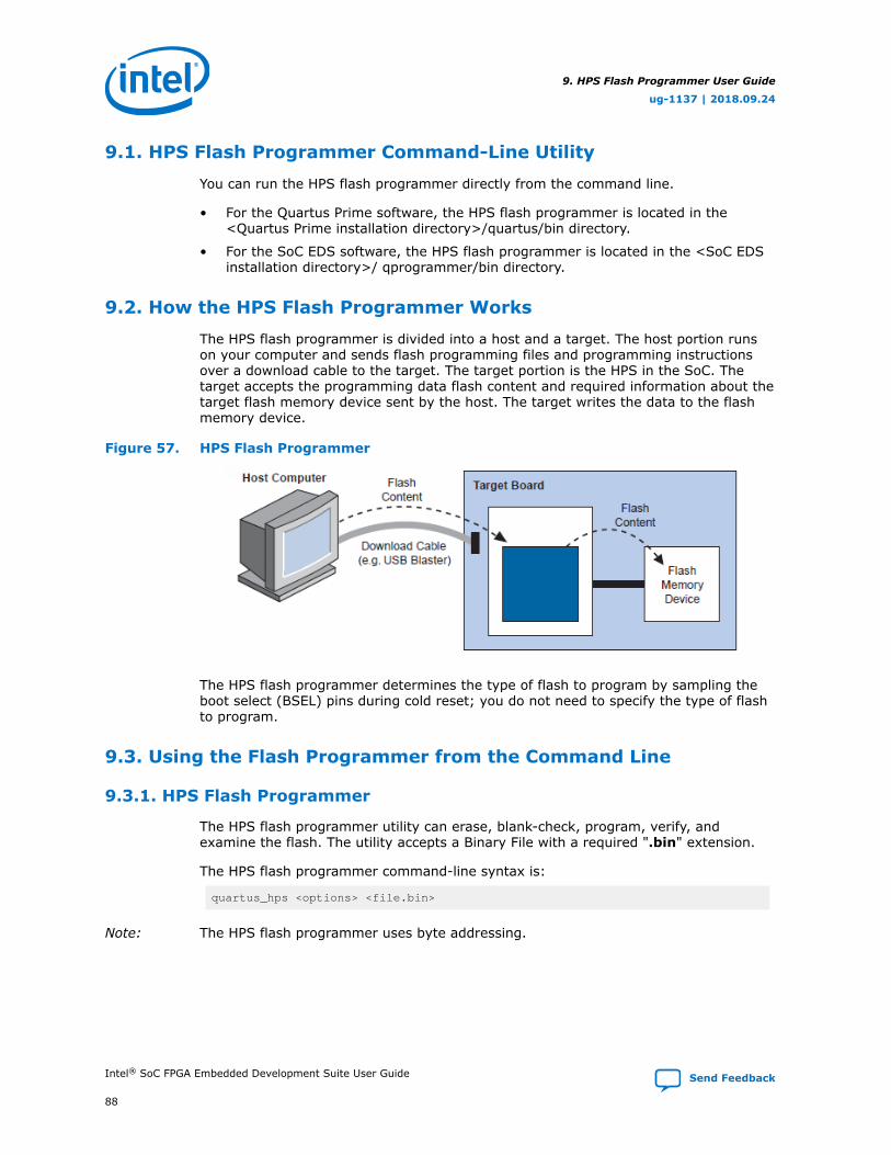
9.1. HPS Flash Programmer Command-Line Utility
You can run the HPS flash programmer directly from the command line.
• For the Quartus Prime software, the HPS flash programmer is located in the<Quartus Prime installation directory>/quartus/bin directory.
• For the SoC EDS software, the HPS flash programmer is located in the <SoC EDSinstallation directory>/ qprogrammer/bin directory.
9.2. How the HPS Flash Programmer Works
The HPS flash programmer is divided into a host and a target. The host portion runson your computer and sends flash programming files and programming instructionsover a download cable to the target. The target portion is the HPS in the SoC. Thetarget accepts the programming data flash content and required information about thetarget flash memory device sent by the host. The target writes the data to the flashmemory device.
Figure 57. HPS Flash Programmer
The HPS flash programmer determines the type of flash to program by sampling theboot select (BSEL) pins during cold reset; you do not need to specify the type of flashto program.
9.3. Using the Flash Programmer from the Command Line
9.3.1. HPS Flash Programmer
The HPS flash programmer utility can erase, blank-check, program, verify, andexamine the flash. The utility accepts a Binary File with a required ".bin" extension.
The HPS flash programmer command-line syntax is:
quartus_hps <options> <file.bin>
Note: The HPS flash programmer uses byte addressing.
9. HPS Flash Programmer User Guide
ug-1137 | 2018.09.24
Intel® SoC FPGA Embedded Development Suite User Guide Send Feedback
88

Table 17. HPS Flash Programmer Parameters
Option Short Option Required Description
--addr -a Yes (if the startaddress is not 0)
This option specifies the start address of the operation tobe performed.
--cable -c Yes This option specifies what download cable to use.To obtain the list of programming cables, run thecommand "jtagconfig". It will list the available cables, likein the following example:jtagconfig
• Intel FPGA Download Cable [USB-0]• Intel FPGA Download Cable [USB-1]• Intel FPGA Download Cable [USB-2]The "-c" parameter can be the number of theprogramming cable, or its name. The following are validexamples for the above case:• -c 1• -c "Intel FPGA Download Cable [USB-2]"
--device -d Yes (if there aremultiple HPS devicesin the chain)
This option specifies the index of the HPS device. The toolwill automatically detect the chain and determine theposition of the HPS device; however, if there are multipleHPS devices in the chain, the targeted device index mustbe specified.
--exit_xip N/A Yes (if the QSPI flashdevice has been putinto XIP mode)
This option exits the QSPI flash device from XIP mode. Anon-zero value has to be specified for the argument. Forexample, quartus_hps -c <cable> -o <operation>--exit_xip=0x80.
--operation -o Yes This option specifies the operation to be performed. Thefollowing operations are supported:• I—Read IDCODE of SOC device and discover Access
Port• S—Read Sislicon ID of the flash• E—Erase flash• B—Blank-check flash• P—Program flash• V—Verify flash• EB—Erase and blank-check flash• BP—Program <BlankCheck> flash• PV—Program and verify flash• BPV—Program (blank-check) and verify flash• X—Examine flashNote: The program begins with erasing the flash
operation before programming the flash by default.
--size -s No This option specifies the number of bytes of data to beperformed by the operation. size is optional.
Note: The following options: repeat and interval must be used together and are optional.The HPS BOOT flow supports up to four images where each image is identical. These options duplicate the operation data;therefore you do not need embedded software to create a large file containing duplicate images.
--repeat -t No repeat—specifies the number of duplicate images for theoperation to perform.
--interval -i No interval—specifies the repeated address. The defaultvalue is 64 kilobytes (KB).
9. HPS Flash Programmer User Guide
ug-1137 | 2018.09.24
Send Feedback Intel® SoC FPGA Embedded Development Suite User Guide
89

9.3.2. HPS Flash Programmer Command Line Examples
Type quartus_hps --help to obtain information about usage. You can also typequartus_hps --help=<option> to obtain more details about each option. Forexample "quartus_hps --help=o".
Example 8. Program File to Address 0 of Flashquartus_hps –c 1 –o P input.bin programs the input file (input.bin) into theflash, starting at flash address 0 using a cable M.
Example 9. Program First 500 Bytes of File to Flash (Decimal)quartus_hps –c 1 –o PV –a 1024 –s 500 input.bin programs the first 500bytes of the input file (input.bin) into the flash, starting at flash address 1024,followed by a verification using a cable M.
Note: Without the prefix "0x" for the flash address, the tool assumes it is decimal.
Example 10. Program First 500 Bytes of File to Flash (Hexadecimal)quartus_hps –c 1 –o PV –a 0x400 –s 500 input.bin programs the first 500bytes of the input file (input.bin) into the flash, starting at flash address 1024,followed by a verification using a cable M.
Note: With the prefix 0x, the tool assumes it is hexadecimal.
Example 11. Program File to Flash Repeating Twice at Every 1 MBquartus_hps –c 1 –o BPV –t 2 –i 0x100000 input.bin programs the inputfile (input.bin) into the flash, using a cable M. The operation repeats itself twice atevery 1 megabyte (MB) of the flash address. Before the program operation, the toolensures the flash is blank. After the program operation, the tool verifies the dataprogrammed.
Example 12. Erase Flash on the Flash Addressesquartus_hps –c 1 –o EB input.bin erases the flash on the flash addresseswhere the input file (input.bin) resides, followed by a blank-check using a cable M.
Example 13. Erase Full Chipquartus_hps –c 1 –o E erases the full chip, using a cable M. When no input file(input.bin) is specified, it will erase all the flash contents.
Example 14. Erase Specified Memory Contents of Flashquartus_hps –c 1 –o E –a 0x100000 –s 0x400000 erases specified memorycontents of the flash. For example, 4 MB worth of memory content residing in theflash address, starting at 1 MB, are erased using a cable M.
Example 15. Examine Data from Flashquartus_hps –c 1 –o X –a 0x98679 –s 56789 output.bin examines 56789bytes of data from the flash with a 0x98679 flash start address, using a cable M.
9. HPS Flash Programmer User Guide
ug-1137 | 2018.09.24
Intel® SoC FPGA Embedded Development Suite User Guide Send Feedback
90
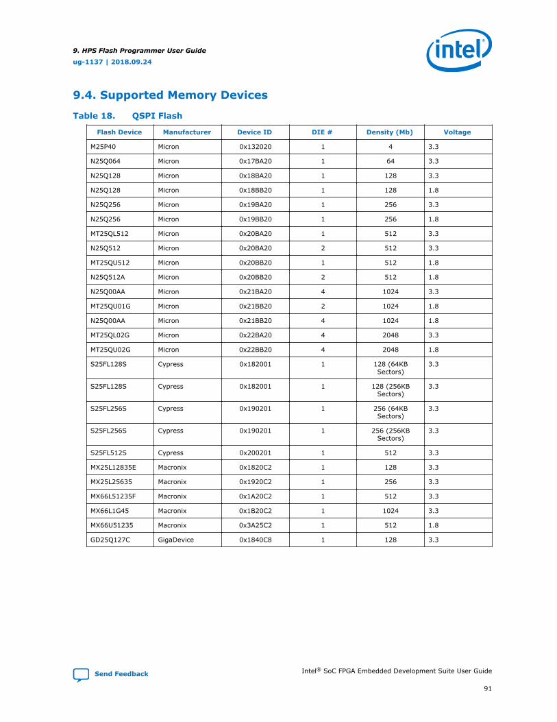
9.4. Supported Memory Devices
Table 18. QSPI Flash
Flash Device Manufacturer Device ID DIE # Density (Mb) Voltage
M25P40 Micron 0x132020 1 4 3.3
N25Q064 Micron 0x17BA20 1 64 3.3
N25Q128 Micron 0x18BA20 1 128 3.3
N25Q128 Micron 0x18BB20 1 128 1.8
N25Q256 Micron 0x19BA20 1 256 3.3
N25Q256 Micron 0x19BB20 1 256 1.8
MT25QL512 Micron 0x20BA20 1 512 3.3
N25Q512 Micron 0x20BA20 2 512 3.3
MT25QU512 Micron 0x20BB20 1 512 1.8
N25Q512A Micron 0x20BB20 2 512 1.8
N25Q00AA Micron 0x21BA20 4 1024 3.3
MT25QU01G Micron 0x21BB20 2 1024 1.8
N25Q00AA Micron 0x21BB20 4 1024 1.8
MT25QL02G Micron 0x22BA20 4 2048 3.3
MT25QU02G Micron 0x22BB20 4 2048 1.8
S25FL128S Cypress 0x182001 1 128 (64KBSectors)
3.3
S25FL128S Cypress 0x182001 1 128 (256KBSectors)
3.3
S25FL256S Cypress 0x190201 1 256 (64KBSectors)
3.3
S25FL256S Cypress 0x190201 1 256 (256KBSectors)
3.3
S25FL512S Cypress 0x200201 1 512 3.3
MX25L12835E Macronix 0x1820C2 1 128 3.3
MX25L25635 Macronix 0x1920C2 1 256 3.3
MX66L51235F Macronix 0x1A20C2 1 512 3.3
MX66L1G45 Macronix 0x1B20C2 1 1024 3.3
MX66U51235 Macronix 0x3A25C2 1 512 1.8
GD25Q127C GigaDevice 0x1840C8 1 128 3.3
9. HPS Flash Programmer User Guide
ug-1137 | 2018.09.24
Send Feedback Intel® SoC FPGA Embedded Development Suite User Guide
91

Table 19. ONFI Compliant NAND Flash
Manufacturer MFC ID Device ID Density (Gb)
Micron 0x2C 0x68 32
Micron 0x2C 0x48 16
Micron 0x2C 0xA1 8
Micron 0x2C 0xF1 8
Note: The above table contains just examples of supported devices. The HPS FlashProgrammer supports all ONFI compliant NAND flash devices that are supported bythe HPS QSPI Flash Controller.
Note: The HPS Flash Programmer supports the Cyclone V SoC, Arria V SoC and Intel Arria 10SoC devices. For more information, refer to the "Supported Flash Devices for CycloneV SoC and Arria V SoC" and the "Supported Flash Devices for Intel Arria 10 SoC" webpages.
Related Information
• Supported Flash Devices for Cyclone V and Arria V SoC
• Supported Flash Devices for Arria 10 SoC
9.5. HPS Flash Programmer User Guide Revision History
Document Version Changes
2018.09.24 Added supported memory devices in the "QSPI Flash" table; and updatedvoltages for several flash devices.
2018.06.18 • Updated chapter to include support for Intel Stratix 10 SoC• Updated chapter to include support for Intel Quartus Prime Pro Edition
2017.05.08 • Intel FPGA rebranding• Rebranded paths and tools for the Standard and Professional versions
2016.11.07 Maintenance release
2016.05.27 Maintenance release
2016.02.17 Added QSPI Flash part number to the QSPI Flash table in the "SupportedMemory Devices" chapter
2015.08.06 Added Intel Arria 10 SoC support
9. HPS Flash Programmer User Guide
ug-1137 | 2018.09.24
Intel® SoC FPGA Embedded Development Suite User Guide Send Feedback
92
10. BareMetal CompilersThe SoC EDS provides the following BareMetal compilers:
• Arm BareMetal Compiler 5 (ARMCC)
• Arm BareMetal Compiler 6 (LLVM-based)
• Mentor Graphics Sourcery™ CodeBench Lite Edition (GCC based)
Related Information
• Mentor Graphics
• SoC EDS Getting Started Guides
10.1. Arm BareMetal Compilers
The Arm BareMetal compilers are part of the Arm DS-5 Intel SoC FPGA Edition.
The Arm BareMetal Compiler 5 targets 32-bit platforms (Cortex-A9 on Cyclone V SoC,Arria V SoC and Intel Arria 10 SoC).
The Arm BareMetal Compiler 6 targets both 32-bit platforms and 64-bit platforms(Cortex-A53 on Intel Stratix 10 SoC).
The Arm BareMetal compilers documentation is integrated in Arm DS-5 Intel SoC FPGAEdition, like with all the Arm DS-5 Intel SoC FPGA Edition components.
10.2. Mentor Code Sourcery Compiler
The BareMetal compiler that is shipped with the SoC EDS is the Mentor GraphicsSourcery CodeBench Lite. For the current version, refer to Table 1 on page 4.
For more information on the Sourcery CodeBench Lite Edition and to download thelatest version of the tools, refer to the Mentor Graphics website.
The GCC-based compiler, arm-altera-eabi, has the following features:
• Targets the Arm processor
• Assumes BareMetal operation
• Uses the standard Arm embedded-application binary interface (EABI) conventions.
The BareMetal compiler is installed as part of the SoC EDS installation in the followingfolder:
<SoC EDS installation directory>/host_tools/mentor/gnu/arm/baremetal
ug-1137 | 2018.09.24
Send Feedback
Intel Corporation. All rights reserved. Intel, the Intel logo, Altera, Arria, Cyclone, Enpirion, MAX, Nios, Quartusand Stratix words and logos are trademarks of Intel Corporation or its subsidiaries in the U.S. and/or othercountries. Intel warrants performance of its FPGA and semiconductor products to current specifications inaccordance with Intel's standard warranty, but reserves the right to make changes to any products and servicesat any time without notice. Intel assumes no responsibility or liability arising out of the application or use of anyinformation, product, or service described herein except as expressly agreed to in writing by Intel. Intelcustomers are advised to obtain the latest version of device specifications before relying on any publishedinformation and before placing orders for products or services.*Other names and brands may be claimed as the property of others.
ISO9001:2015Registered

The Embedded Command Shell sets the correct environment PATH variables for theBareMetal compilation tools to be invoked. You can open the shell from the <SoC EDSinstallation directory>. After starting the shell, commands like arm-altera-eabi-gcccan be invoked directly. When the Arm Development Studio 5 Intel SoC FPGA Editionenvironment is started from the embedded command shell, it inherits the environmentsettings, and it can call these compilation tools directly.
You can also use the full path to the compilation tools:
<SoC EDS installation directory>/host_tools/mentor/gnu/arm/baremetal/bin
The BareMetal compiler is installed with full documentation, located at:
<SoC EDS installation directory>/host_tools/mentor/gnu/arm/baremetal/share/doc/sourceryg++-arm-altera-eabi
The documentation is offered in four different formats to accommodate various userpreferences:
• HTML files
• Info files
• Man pages
• PDF files
Among the provided documents are:
• Compiler manual
• Assembler manual
• Linker manual
• Binutils manual
• GDB manual
• Getting Started Guides(4)
• Libraries Manual
Related Information
• Differences Between Standard and Professional Editions on page 5
• SoCEDSGettingStarted
10.3. BareMetal Compilers Revision History
Document Version Changes
2018.09.24 Maintenance release
2018.06.18 • Updated chapter to include support for Intel Stratix 10 SoC• Added information that the Arm BareMetal Compiler 6 targets both 32-bit
and 64-bit platforms
continued...
(4) The Getting Started Guides are located on the "SoCEDSGettingStarted" web page on the IntelFPGA Wiki.
10. BareMetal Compilers
ug-1137 | 2018.09.24
Intel® SoC FPGA Embedded Development Suite User Guide Send Feedback
94

Document Version Changes
2017.05.08 • Intel FPGA rebranding• Rebranded paths and tools for the Standard and Professional versions
2016.11.07 Added a "Mentor Code Sourcery Compiler" section
2016.05.27 Maintenance release
2016.02.17 Updated the compiler version for Mentor Graphics Sourcery CodeBench LiteEdition
2015.08.06 Added Intel Arria 10 SoC support
10. BareMetal Compilers
ug-1137 | 2018.09.24
Send Feedback Intel® SoC FPGA Embedded Development Suite User Guide
95
11. SD Card Boot UtilityThe SoC EDS SD card boot utility is a tool for updating the boot software on an SDcard.
The Preloader is typically stored in a custom partition (with type = 0xA2) on the SDcard. Optionally, the next boot stage (usually the Bootloader) can also be stored onthe same custom partition.
Since it is a custom partition without a file-system, the Preloader, Bootloader, or bothcannot be updated by copying the new file to the card; and a software tool is needed.
The SD card boot utility allows you to update the Preloader, Bootloader, or both on aphysical SD card or a disk image file. The utility is not intended to create a newbootable SD card or disk image file from scratch. In order to do that, it isrecommended to use fdisk on a Linux host OS.
Note: The SD Card Boot Utility tool is not needed for Intel Stratix 10 SoC devices.
Related Information
Linux Software Development Tools on page 99
11.1. Usage Scenarios
This utility is intended to update boot software on that resides on an existing:
• Existing SD card
• Existing disk image file
The tool supports updating the following:
• Cyclone V SoC and Arria V SoC Preloader—The Preloader file needs to have themkpimage header, as required by the bootROM.
• Cyclone V SoC and Arria V SoC Bootloader—The Bootloader file needs to have themkimage header, as required by the Preloader.
• Intel Arria 10 SoC Bootloader—The Bootloader needs to have the mkpimageheader, as required by the bootROM.
Note: Both mkpimage and mkimage tools are delivered as part of SoC EDS.
The tool only updates the custom partition that stores the Intel SoC boot code. Therest of the SD card or disk image file is not touched. This includes the Master BootRecord (MBR) and any other partitions (such as FAT and EXT3) and free space.
ug-1137 | 2018.09.24
Send Feedback
Intel Corporation. All rights reserved. Intel, the Intel logo, Altera, Arria, Cyclone, Enpirion, MAX, Nios, Quartusand Stratix words and logos are trademarks of Intel Corporation or its subsidiaries in the U.S. and/or othercountries. Intel warrants performance of its FPGA and semiconductor products to current specifications inaccordance with Intel's standard warranty, but reserves the right to make changes to any products and servicesat any time without notice. Intel assumes no responsibility or liability arising out of the application or use of anyinformation, product, or service described herein except as expressly agreed to in writing by Intel. Intelcustomers are advised to obtain the latest version of device specifications before relying on any publishedinformation and before placing orders for products or services.*Other names and brands may be claimed as the property of others.
ISO9001:2015Registered
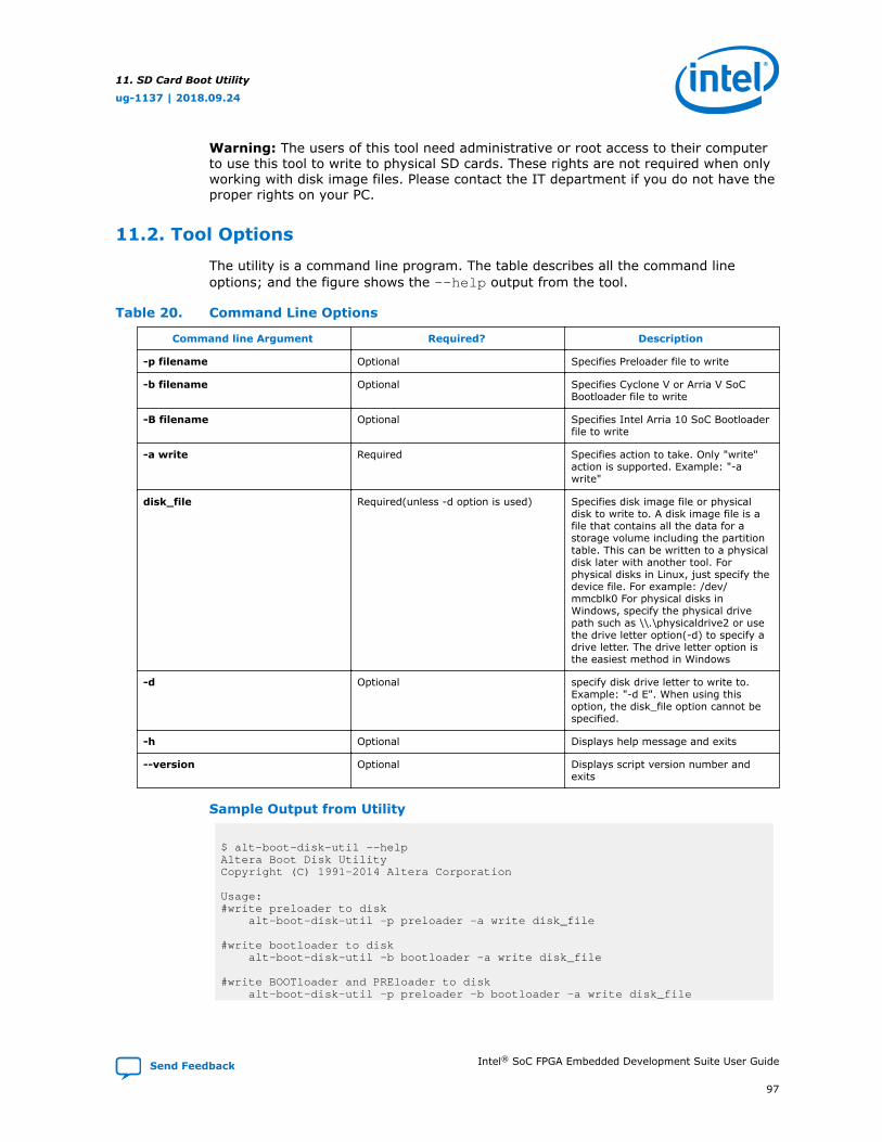
Warning: The users of this tool need administrative or root access to their computerto use this tool to write to physical SD cards. These rights are not required when onlyworking with disk image files. Please contact the IT department if you do not have theproper rights on your PC.
11.2. Tool Options
The utility is a command line program. The table describes all the command lineoptions; and the figure shows the --help output from the tool.
Table 20. Command Line Options
Command line Argument Required? Description
-p filename Optional Specifies Preloader file to write
-b filename Optional Specifies Cyclone V or Arria V SoCBootloader file to write
-B filename Optional Specifies Intel Arria 10 SoC Bootloaderfile to write
-a write Required Specifies action to take. Only "write"action is supported. Example: "-awrite"
disk_file Required(unless -d option is used) Specifies disk image file or physicaldisk to write to. A disk image file is afile that contains all the data for astorage volume including the partitiontable. This can be written to a physicaldisk later with another tool. Forphysical disks in Linux, just specify thedevice file. For example: /dev/mmcblk0 For physical disks inWindows, specify the physical drivepath such as \\.\physicaldrive2 or usethe drive letter option(-d) to specify adrive letter. The drive letter option isthe easiest method in Windows
-d Optional specify disk drive letter to write to.Example: "-d E". When using thisoption, the disk_file option cannot bespecified.
-h Optional Displays help message and exits
--version Optional Displays script version number andexits
Sample Output from Utility
$ alt-boot-disk-util --helpAltera Boot Disk UtilityCopyright (C) 1991-2014 Altera Corporation
Usage:#write preloader to disk alt-boot-disk-util -p preloader -a write disk_file
#write bootloader to disk alt-boot-disk-util -b bootloader -a write disk_file
#write BOOTloader and PREloader to disk alt-boot-disk-util -p preloader -b bootloader -a write disk_file
11. SD Card Boot Utility
ug-1137 | 2018.09.24
Send Feedback Intel® SoC FPGA Embedded Development Suite User Guide
97

#write Arria10 Bootloader to disk alt-boot-disk-util -B a10bootloader -a write disk_file
#write BOOTloader and PREloader to disk drive 'E' alt-boot-disk-util -p preloader -b bootloader -a write -d E
Options: --version show program's version number and exit -h, --help show this help message and exit -b FILE, --bootloader=FILE bootloader image file' -p FILE, --preloader=FILE preloader image file' -a ACTION, --action=ACTION only supports 'write' action' -B FILE, --a10-bootloader=FILE arria10 bootloader image file -d DRIVE, --drive=DRIVE specify disk drive letter to write to
11.3. SD Card Boot Utility Revision History
Document Version Changes
2018.09.24 Maintenance release
2018.06.18 • Updated chapter to indicate that the SD Card Boot Utility is not needed forIntel Stratix 10 SoC devices
2017.05.08 • Intel FPGA rebranding• Rebranded paths and tools for the Standard and Professional versions
2016.11.07 Maintenance release
2016.05.27 Maintenance release
2016.02.17 Maintenance release
2015.08.06 Added Intel Arria 10 SoC support
11. SD Card Boot Utility
ug-1137 | 2018.09.24
Intel® SoC FPGA Embedded Development Suite User Guide Send Feedback
98

12. Linux Software Development ToolsThe Linux software development tools are listed below. The Linux compiler and thelinux device tree generator are described in the following sections of this chapter.
• Linux compiler
• SD card boot utility
• Linux device tree generator (DTG)
Related Information
SD Card Boot Utility on page 96
12.1. Linux Compiler
The Linaro Linux compiler is shipped with the SoC EDS. For the current version, referto Table 1 on page 4.
Note: For Intel Stratix 10 SoC devices, it is recommended to use the Linaro compiler from:https://releases.linaro.org/components/toolchain/binaries/7.2-2017.11/aarch64-linux-gnu/gcc-linaro-7.2.1-2017.11-x86_64_aarch64-linux-gnu.tar.xz instead of the Linux compiler shipped withthe SoC EDS.
For more information about the Linux compiler and to download the latest version ofthe tools, refer to the download page at the Linaro website.
The compiler is a GCC-based arm-linux-gnueabihf port. It targets the Armprocessor, it assumes the target platform is running Linux, and it uses the GNUembedded-application binary interface (EABI) hard-float (HF) conventions.
The Linux compiler is installed as part of the Arm DS-5 Intel SoC FPGA Edition, whichis installed as part of the SoC EDS. The compilation tools are located at:
<SoC EDS installation directory>/ds-5/bin.
The Linux compiler is installed with full documentation, located at:
<SoC EDS installation directory>/ds-5/documents/gcc.
The documents are provided as HTML files. Some of the provided documents are:
• Compiler manual
• Assembler manual
• Linker manual
ug-1137 | 2018.09.24
Send Feedback
Intel Corporation. All rights reserved. Intel, the Intel logo, Altera, Arria, Cyclone, Enpirion, MAX, Nios, Quartusand Stratix words and logos are trademarks of Intel Corporation or its subsidiaries in the U.S. and/or othercountries. Intel warrants performance of its FPGA and semiconductor products to current specifications inaccordance with Intel's standard warranty, but reserves the right to make changes to any products and servicesat any time without notice. Intel assumes no responsibility or liability arising out of the application or use of anyinformation, product, or service described herein except as expressly agreed to in writing by Intel. Intelcustomers are advised to obtain the latest version of device specifications before relying on any publishedinformation and before placing orders for products or services.*Other names and brands may be claimed as the property of others.
ISO9001:2015Registered

• Binutils manual
• GDB manual
• Getting Started Guide
Related Information
• Linaro Website
• Differences Between Standard and Professional Editions on page 5
12.2. Linux Device Tree Generator
A device tree is a data structure that describes the underlying hardware to anoperating system - primarily Linux. By passing this data structure to the OS kernel, asingle OS binary may be able to support many variations of hardware. This flexibility isparticularly important when the hardware includes an FPGA.
The Linux Device Tree Generator (DTG) tool is part of SoC EDS and is used to createLinux device trees for the Cyclone V SoC, Arria V SoC, and Intel Arria 10 SoC systemsthat contain FPGA designs created using Platform Designer (Standard). The generateddevice tree describes the HPS peripherals, selected FPGA Soft IP, and peripherals thatare board dependent.
Note: The Intel Arria 10 SoC Bootloader also has an associated Device Tree called BootloaderDevice Tree that is created and managed by the BSP Editor tool.
Note: The Linux Device Tree Generator does not support the Intel Stratix 10 SoC devices.
Warning: The Linux Device Tree Generator is tested with and supports only the Linuxkernel version targeted by the associated GSRD. It is not recommended to use theLinux Device Tree Generator if your design targets a different Linux kernel version.Instead, it is recommended to manage the Device Tree manually by using the DeviceTree files provided by the kernel as a baseline, and by adding the FPGA IP and boardinformation manually.
Related Information
• Intel FPGA WikiFor more information about the Linux DTG, refer to the Intel FPGA Wikiwebsite.
• Linux Device Tree Generator User GuideFor more details, navigate to the Device Tree Generator User Guide locatedon the Device Tree Generator Documentation page on the Rocketboardswebsite.
12. Linux Software Development Tools
ug-1137 | 2018.09.24
Intel® SoC FPGA Embedded Development Suite User Guide Send Feedback
100

12.3. Linux Software Development Tools Revision History
Document Version Changes
2018.09.24 Maintenance release
2018.06.18 • Updated chapter to include support for Intel Stratix 10 SoC• Added information about using the Linaro compiler instead of the Linux
compiler• Updated the chapter to indicate that the Linux Device Tree Generator does
not support the Intel Stratix 10 SoC devices.
2017.05.08 • Intel FPGA rebranding• Rebranded paths and tools for the Standard and Professional versions
2016.11.07 Maintenance release
2016.05.27 Maintenance release
2016.02.17 Maintenance release
2015.08.06 Added Intel Arria 10 SoC support
12. Linux Software Development Tools
ug-1137 | 2018.09.24
Send Feedback Intel® SoC FPGA Embedded Development Suite User Guide
101

13. Support and FeedbackIntel values your feedback. Please contact your Intel TSFAE or submit a servicerequest at myAltera to report software bugs, potential enhancements, or obtain anyadditional information.
Related Information
• SoCEDSGettingStartedFor more information about getting started, refer to the SoCEDSGettingStartedpage on the Intel FPGA Wiki.
• myAltera Account Sign In
13.1. Support and Feedback Revision History
Document Version Changes
2018.09.24 Maintenance release
2018.06.18 Updated chapter to include support for Intel Stratix 10 SoC
2017.05.08 • Intel FPGA rebranding• Rebranded paths and tools for the Standard and Professional versions
2016.11.07 Maintenance release
2016.05.27 Maintenance release
2016.02.17 Maintenance release
2015.08.06 Added Intel Arria 10 SoC support
ug-1137 | 2018.09.24
Send Feedback
Intel Corporation. All rights reserved. Intel, the Intel logo, Altera, Arria, Cyclone, Enpirion, MAX, Nios, Quartusand Stratix words and logos are trademarks of Intel Corporation or its subsidiaries in the U.S. and/or othercountries. Intel warrants performance of its FPGA and semiconductor products to current specifications inaccordance with Intel's standard warranty, but reserves the right to make changes to any products and servicesat any time without notice. Intel assumes no responsibility or liability arising out of the application or use of anyinformation, product, or service described herein except as expressly agreed to in writing by Intel. Intelcustomers are advised to obtain the latest version of device specifications before relying on any publishedinformation and before placing orders for products or services.*Other names and brands may be claimed as the property of others.
ISO9001:2015Registered