1771-6.5.32, absolute encoder module user manual
TRANSCRIPT
User
Manual
Absolute EncoderModule
(Cat. No. 1771-DE)
Allen�Bradley

Using This Manual 1�1. . . . . . . . . . . . . . . . . . . . . . . . . . . . . . .
Chapter Objectives 1�1. . . . . . . . . . . . . . . . . . . . . . . . . . . . . . . . . . .
What This Manual Contains 1�1. . . . . . . . . . . . . . . . . . . . . . . . . . . .
Audience 1�1. . . . . . . . . . . . . . . . . . . . . . . . . . . . . . . . . . . . . . . . . .
Warnings and Cautions 1�2. . . . . . . . . . . . . . . . . . . . . . . . . . . . . . .
Summary 1�2. . . . . . . . . . . . . . . . . . . . . . . . . . . . . . . . . . . . . . . . .
Introducing the Absolute Encoder Module 2�1. . . . . . . . . . . . .
Chapter Objectives 2�1. . . . . . . . . . . . . . . . . . . . . . . . . . . . . . . . . . .
Example Applications 2�1. . . . . . . . . . . . . . . . . . . . . . . . . . . . . . . . .
Module Functions 2�1. . . . . . . . . . . . . . . . . . . . . . . . . . . . . . . . . . . .
Compatible Processors 2�2. . . . . . . . . . . . . . . . . . . . . . . . . . . . . . .
Compatible Encoders 2�2. . . . . . . . . . . . . . . . . . . . . . . . . . . . . . . . .
State of Outputs Upon Loss of Input Power 2�2. . . . . . . . . . . . . . . . . .
Module Description 2�3. . . . . . . . . . . . . . . . . . . . . . . . . . . . . . . . . .
Electrostatic Discharge 2�5. . . . . . . . . . . . . . . . . . . . . . . . . . . . . . . .
Specifications 2�6. . . . . . . . . . . . . . . . . . . . . . . . . . . . . . . . . . . . . .
Summary 2�7. . . . . . . . . . . . . . . . . . . . . . . . . . . . . . . . . . . . . . . . .
Configuring and Installing Your Module 3�1. . . . . . . . . . . . . . .
Chapter Objectives 3�1. . . . . . . . . . . . . . . . . . . . . . . . . . . . . . . . . . .
Electrostatic Discharge 3�1. . . . . . . . . . . . . . . . . . . . . . . . . . . . . . . .
Setting Configuration Plugs 3�1. . . . . . . . . . . . . . . . . . . . . . . . . . . . .
Response to External Fault 3�4. . . . . . . . . . . . . . . . . . . . . . . . . . . . .
Keying 3�4. . . . . . . . . . . . . . . . . . . . . . . . . . . . . . . . . . . . . . . . . . .
Power Requirements 3�5. . . . . . . . . . . . . . . . . . . . . . . . . . . . . . . . .
Wiring�Arm Connections 3�8. . . . . . . . . . . . . . . . . . . . . . . . . . . . . . .
Installing the Module 3�11. . . . . . . . . . . . . . . . . . . . . . . . . . . . . . . . . .
Module/Processor Communication 4�1. . . . . . . . . . . . . . . . . .
Chapter Objectives 4�1. . . . . . . . . . . . . . . . . . . . . . . . . . . . . . . . . . .
Block Transfer 4�1. . . . . . . . . . . . . . . . . . . . . . . . . . . . . . . . . . . . . .
Block�transfer�write Data 4�1. . . . . . . . . . . . . . . . . . . . . . . . . . . . . .
Write�Data Throughput Time 4�4. . . . . . . . . . . . . . . . . . . . . . . . . . . .
Block�transfer�read Data 4�4. . . . . . . . . . . . . . . . . . . . . . . . . . . . . . .
Programming Example 4�5. . . . . . . . . . . . . . . . . . . . . . . . . . . . . . . .
Programming Considerations 4�7. . . . . . . . . . . . . . . . . . . . . . . . . . .
Summary 4�7. . . . . . . . . . . . . . . . . . . . . . . . . . . . . . . . . . . . . . . . .
Table of Contents
Table of Contentsii
Offset Feature 5�1. . . . . . . . . . . . . . . . . . . . . . . . . . . . . . . . . .
Offset Feature 5�1. . . . . . . . . . . . . . . . . . . . . . . . . . . . . . . . . . . . . .
Offset Words 5�2. . . . . . . . . . . . . . . . . . . . . . . . . . . . . . . . . . . . . . .
Programming Considerations with Offset 5�6. . . . . . . . . . . . . . . . . . .
Troubleshooting 6�1. . . . . . . . . . . . . . . . . . . . . . . . . . . . . . . .
Chapter Objectives 6�1. . . . . . . . . . . . . . . . . . . . . . . . . . . . . . . . . . .
Causes of Block�transfer Errors 6�1. . . . . . . . . . . . . . . . . . . . . . . . . .
Errors Indicated by Diagnostic Bits 6�2. . . . . . . . . . . . . . . . . . . . . . .
Summary 6�2. . . . . . . . . . . . . . . . . . . . . . . . . . . . . . . . . . . . . . . . .
Block�transfer Timing A�1. . . . . . . . . . . . . . . . . . . . . . . . . . . . . . . . .
Block�transfer Timing for PLC�2 Family Processors A�1. . . . . . . . . . . .
Block�transfer Timing for PLC�3 Family Processors A�8. . . . . . . . . . . .
Application Considerations B�1. . . . . . . . . . . . . . . . . . . . . . . . . . . . .
Application Considerations B�1. . . . . . . . . . . . . . . . . . . . . . . . . . . . .
Block�transfer Ladder Diagram Examples C�1. . . . . . . . . . . . .
Bidirectional Block�transfer for PLC�2 Family Processors C�1. . . . . . . .
Bidirectional Block�transfer for PLC�3 Processors C�4. . . . . . . . . . . . .
Read�only Block�transfer for PLC�2 Family Processors C�6. . . . . . . . .
Bit and Word Descriptions of Block-transfer Data D�1. . . . . . .
Block-transfer-write Data D�1. . . . . . . . . . . . . . . . . . . . . . . . . . . . . .
Block-transfer-read Data D�2. . . . . . . . . . . . . . . . . . . . . . . . . . . . . .
Connection Diagrams for Allen�Bradley Encoders E�1. . . . . .
Connection Diagrams for Allen�Bradley Encoders E�1. . . . . . . . . . . . .
0 to 359�count, 10�bit, BCD, Single�ended Output E�1. . . . . . . . . . . . .
0 to 255�count, 8�bit, Standard Gray, Single�ended Output E�3. . . . . . .
0 to 359�count, 10�bit, BCD, Single�ended Output, Latching E�4. . . . . .
Glossary F�1. . . . . . . . . . . . . . . . . . . . . . . . . . . . . . . . . . . . . .
Chapter
1
1�1
Using This Manual
Read this chapter to familiarize yourself with this manual. It tells youhow to use the manual properly and efficiently.
This manual contains 5 chapters and 6 appendices:
Chapter/Appendix
Title What's Covered
1 Using This Manual Manual's purpose, audience, and contents
2 Introducing the AbsoluteEncoder Module
Module description, features, and hardwarecomponents
3 Configuring and InstallingYour Module
Feature selection and installation procedures
4 Module/ProcessorCommunication
Words and file parameters of block�transferdata
5 Offset Feature Programming to compensate for shaft offset
6 Troubleshooting Troubleshooting guide
A Block-transfer Timing Instructions for determining block�transfertiming
B Application Consideration Encoder shaft speed
C Block-transfer LadderDiagram Examples
Examples of block�transfer programming
D Biat and Word Descriptionof Block-transfer Data
Details of block�transfer file data
E Glossary
F Index
In this manual we assume that you know how to:
program and operate an Allen-Bradley programmable controller program block-transfer instructions
Chapter Objectives
What This Manual Contains
Audience
Using This ManualChapter 1
1�2
If you do not know how to do either of these, read the user’s manual ofyour processor. Refer to our Publications Index (publication SD499) for acomplete list of publications.
Throughout this manual we include special notes to alert you to possibleinjury to personnel or damage to equipment under specific circumstances.
WARNING: tells you when people may be injured ifprocedures are not followed properly.
CAUTION: tells you when machinery may be damaged ifprocedures are not followed properly.
This chapter told you how to use this manual efficiently. The next chapterintroduces you to the absolute encoder module.
Warnings and Cautions
Summary
Chapter
2
2�1
Introducing the Absolute Encoder Module
This chapter describes:
example applications of the absolute encoder module functions of the module Allen-Bradley processors compatible with the absolute encoder module encoders you can use with the module module specifications
The absolute encoder module is usually used for:
absolute-position feedback high-speed response to position based on encoder values immunity to loss of position from power loss or power interruptions
The Absolute Encoder Module (cat. no. 1771-DE) is an intelligent modulethat provides high-speed response to machine position independently ofthe programmable controller scan. It can:
monitor the position of an absolute encoder that has up to 12 bits control up to eight high-current outputs based on comparisons between
encoder position and your preset values provide throughput for all eight outputs in less than 200 us communicate with the programmable controller through block transfers return the status of outputs and the position of an absolute encoder to
the programmable controller
In addition, the module can switch 2A DC per output with no deratingwhen all outputs are on, allowing 16A continuous per module.
Chapter Objectives
Example Applications
Module Functions
Introducing the Absolute Encoder ModuleChapter 2
2�2
You can use the absolute encoder module with any Allen-Bradleyprogrammable controller that uses block-transfer programming in bothlocal and remote 1771 I/O systems. Processors that are compatible withthe module include:
Mini PLC-2 (cat. no. 1772-LN3) PLC-2/20 (cat. no. 1772-LP1, -LP2) PLC-2/30 (cat. no. 1772-LP3) PLC-3 (cat. no. 1775-L1, -L2) Mini-PLC-2/15 (cat. no. 1772-LV) Mini-PLC-2/05 (cat. no. 1772-LS, -LSP)
You can use Allen-Bradley absolute encoders that use up to 12 bits withthe absolute encoder module. Allen-Bradley encoders with the followingbulletin numbers are compatible with the absolute encoder module:
Bulletin 845A Bulletin 845B Bulletin 845C
The module is also compatible with absolute encoders that have thefollowing specifications:
single-ended or differential encoder output signals TTL-compatibility (output drivers) capability of sinking 11mA (single-ended) or 18mA (differential) per
channel BCD, natural binary, or standard Gray code format
You can select the state in which the outputs will be if the module losesinput power. A configuration plug on the right printed-circuit boardallows the outputs to:
turn off remain in their state at loss of input power
Compatible Processors
Compatible Encoders
State of Outputs Upon Loss ofInput Power
Introducing the Absolute Encoder ModuleChapter 2
2�3
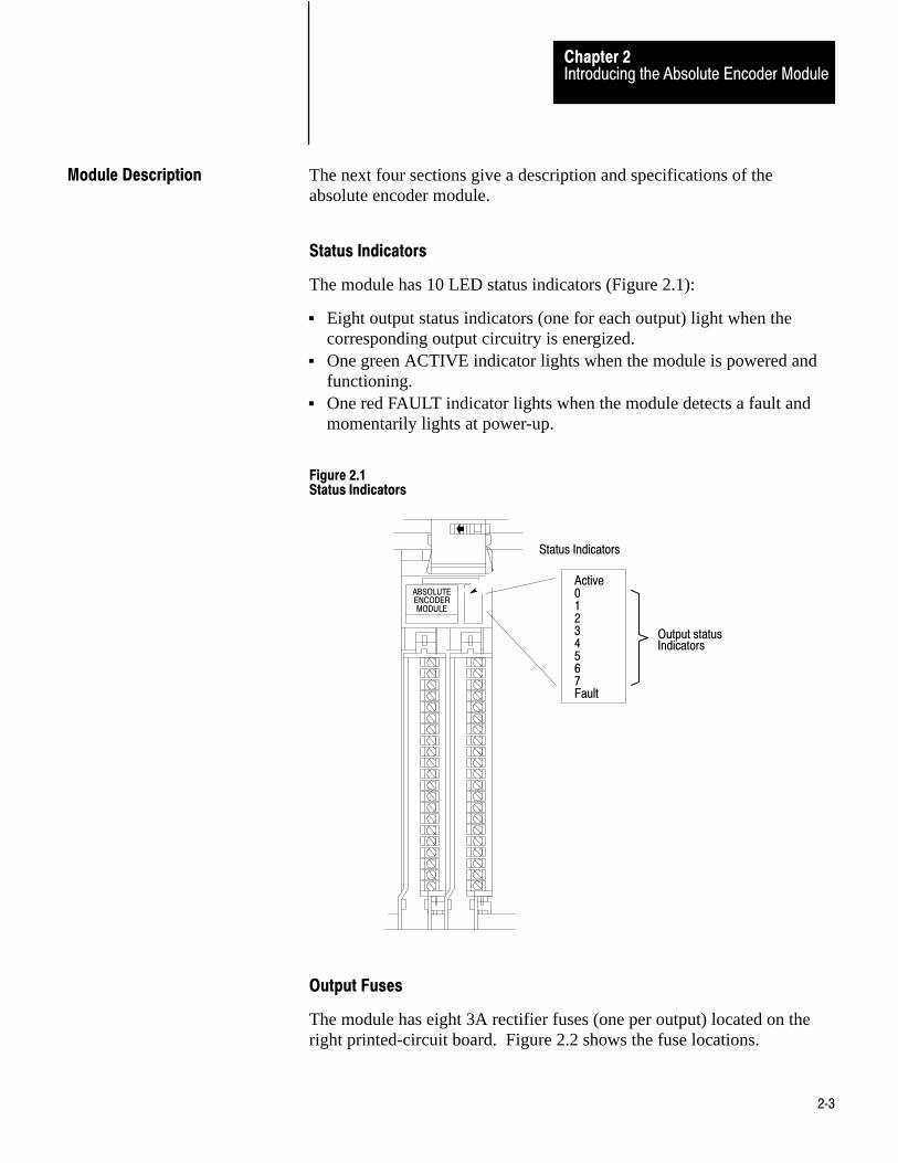
The next four sections give a description and specifications of theabsolute encoder module.
Status Indicators
The module has 10 LED status indicators (Figure 2.1):
Eight output status indicators (one for each output) light when thecorresponding output circuitry is energized.
One green ACTIVE indicator lights when the module is powered andfunctioning.
One red FAULT indicator lights when the module detects a fault andmomentarily lights at power-up.
Figure 2.1Status Indicators
ABSOLUTEENCODERMODULE
Active01234567Fault
Output statusIndicators
Status Indicators
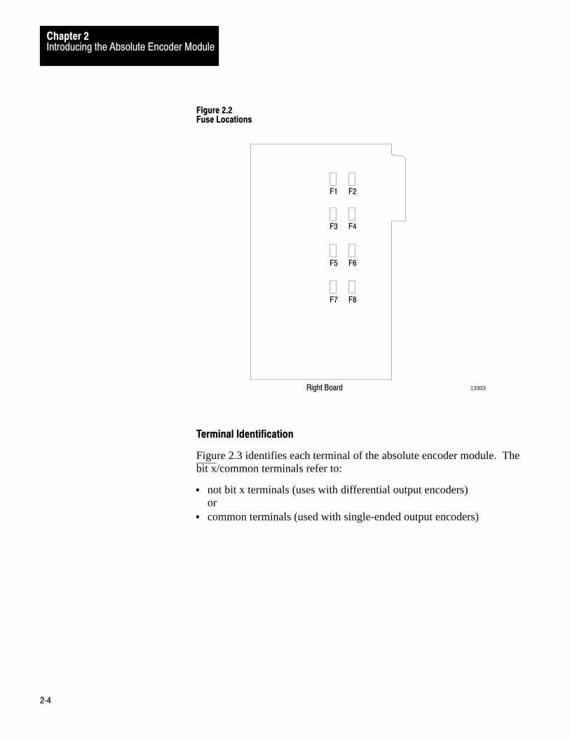
Output Fuses
The module has eight 3A rectifier fuses (one per output) located on theright printed-circuit board. Figure 2.2 shows the fuse locations.
Module Description
Introducing the Absolute Encoder ModuleChapter 2
2�4
Figure 2.2Fuse Locations
F1 F2
F3 F4
F5 F6
F7 F8
Right Board 13303
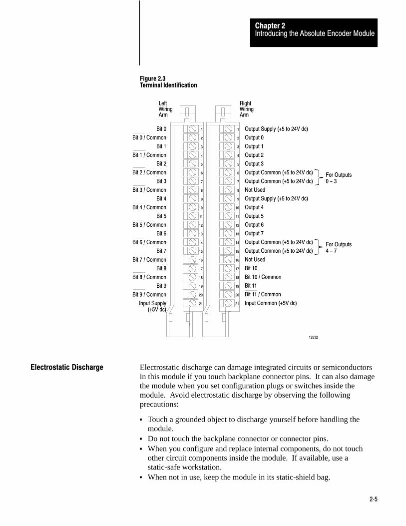
Terminal Identification
Figure 2.3 identifies each terminal of the absolute encoder module. Thebit x/common terminals refer to:
not bit x terminals (uses with differential output encoders) or
common terminals (used with single-ended output encoders)
Introducing the Absolute Encoder ModuleChapter 2
2�5
Figure 2.3Terminal Identification
1
2
3
4
5
6
7
8
9
10
11
12
13
14
15
16
17
18
19
20
21
1
2
3
4
5
6
7
8
9
10
11
12
13
14
15
16
17
18
19
20
21
Output Supply (+5 to 24V dc)
Output 0
Output 1
Output 2
Output 3
Output Common (+5 to 24V dc)
Output Common (+5 to 24V dc)
Not Used
Output Supply (+5 to 24V dc)
Output 4
Output 5
Output 6
Output 7
Output Common (+5 to 24V dc)
Output Common (+5 to 24V dc)
Not Used
Bit 10
Bit 10 / Common
Bit 11
Bit 11 / Common
Input Common (+5V dc)
Bit 0
Bit 0 / Common
Bit 1
Bit 1 / Common
Bit 2
Bit 2 / Common
Bit 3
Bit 3 / Common
Bit 4
Bit 4 / Common
Bit 5
Bit 5 / Common
Bit 6
Bit 6 / Common
Bit 7
Bit 7 / Common
Bit 8
Bit 8 / Common
Bit 9
Bit 9 / Common
Input Supply(+5V dc)
12832
LeftWiringArm
RightWiringArm
For Outputs0 - 3
For Outputs4 - 7
Electrostatic discharge can damage integrated circuits or semiconductorsin this module if you touch backplane connector pins. It can also damagethe module when you set configuration plugs or switches inside themodule. Avoid electrostatic discharge by observing the followingprecautions:
Touch a grounded object to discharge yourself before handling themodule.
Do not touch the backplane connector or connector pins. When you configure and replace internal components, do not touch
other circuit components inside the module. If available, use astatic-safe workstation.
When not in use, keep the module in its static-shield bag.
Electrostatic Discharge
Specifications
Introducing the Absolute Encoder ModuleChapter 2
2�6
CAUTION: Electrostatic discharge can degrade performance ordamage the module. Handle as stated above.
Module Location Any 1771�I/O chassis; any 2�slot I.O
group
Input Power Supply +5V DC +0.25V (total output voltage tolerance includes line
regulation, load regulation, drift, and ripple)
Number of Inputs Up to 12 encoder input bits per
module
Current Requirement300mA (maximum)
Encoder FormatsBCDNatural binaryStandard Gray
Number of Outputs8
Digital ResolutionUp to one part in 4,095 withnatural binary and standardGray encodersUp to one part in 999 withBCD encoders
Output Current Rating2A sourced per output (noderating with all outputs on)
High�true LogicFrom totem pole, opencollector, or differential linedriversCan select direction ofrotation of increasing positionfor Gray code encoders
VA Rating48W per output384W per module
Surge Rating4A for l0 ms
Input Voltage Range and Logic StateLogic 1: 1.7V DCLogic 0:0.0V to 0.6V DC
Input and Output Isolation1500V RMS
Input Current per Channel(sunk by encoder device)
ll mA for single�ended driversl8 mA for differential drivers
Output Power SupplySelectable : +5 to +24V DC
Maximum input Frequency50 KHz
Backplane Current800 mA at 5V DC
Encoder Data Settling Time100 ns
Output Fuses3A rectifier fuses (Littelfuse322003, Buss GBB003, orequivalent)
Introducing the Absolute Encoder ModuleChapter 2
2�7
New Position Throughput Time200 us
Environmental ConditionsOperating Temperature0 to 60o C (32 to 140oF)Storage Temperature�40 to 85oC (�40 to 185oF)Relative Humidity5 to 95% (withoutcondensation)
New Write�data Throughput Time4.7 ms
Keying (for slot 0 only)Between 2 and 4Between 26 and 28
Torque for wiring arm connections9 inch�pounds
This chapter described the absolute encoder module, its functions andapplications, and the processors and encoders with which it is compatible.The next chapter tells you how to configure and install the module.
Summary
Chapter
3
3�1
Configuring and Installing Your Module
This chapter tells you how to:
select module features by setting configuration plugs power module input circuitry and output devices key the module make wiring arm connections install the module
Electrostatic discharge can damage integrated dircuits or semiconductorsin this module if you touch backplane connector pins. It can also damagethe module when you set configuration plugs or switches inside themodule. Avoid electrostatic discharge by observing the followingprecautions:
Touch a grounded object to discharge yourself before handling themodule.
Do not touch the backplane connector or connector pins. When you configure and replace internal components, do not touch
other circuit components inside the module. If available, use astatic-safe work station.
When not in use, keep the module in its static-shield bag.
CAUTION: Electrostatic discharge can degrade performanceor damage the module. Handle as stated above.
You can choose various module features by setting configuration plugs.The module is factory-set for use with a BCD differential output encoder.To access the configuration plugs, lay the module on its right side andremove the cover.
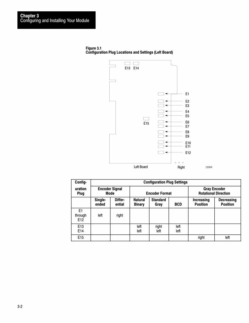
The configuration plug sockets are labeled E1 through E15 on the leftprinted-circuit board and E1 on the right printed-circuit board. Locate theconfiguration plugs with the board positioned as shown in Figure 3.1 andFigure 3.2. Each plug is inserted on two pins of a three-pin connector.You change the position of the plugs in a left-right or up-down direction.
Chapter Objectives
Electrostatic Discharge
Setting Configuration Plugs
Configuring and Installing Your ModuleChapter 3
3�2
Figure 3.1Configuration Plug Locations and Settings (Left Board)
E13
Left Board 13304Right
E14
E15
E1
E2E3
E4E5
E6E7
E8E9
E10E11
E12
Config� Configuration Plug Settings
urationPlug
Encoder SignalMode Encoder Format
Gray EncoderRotational Direction
Single�ended
Differ�ential
NaturalBinary
StandardGray BCD
IncreasingPosition
DecreasingPosition
E1through
E12left right
E13E14
leftleft
rightleft
leftleft
E15 right left
Configuring and Installing Your ModuleChapter 3
3�3
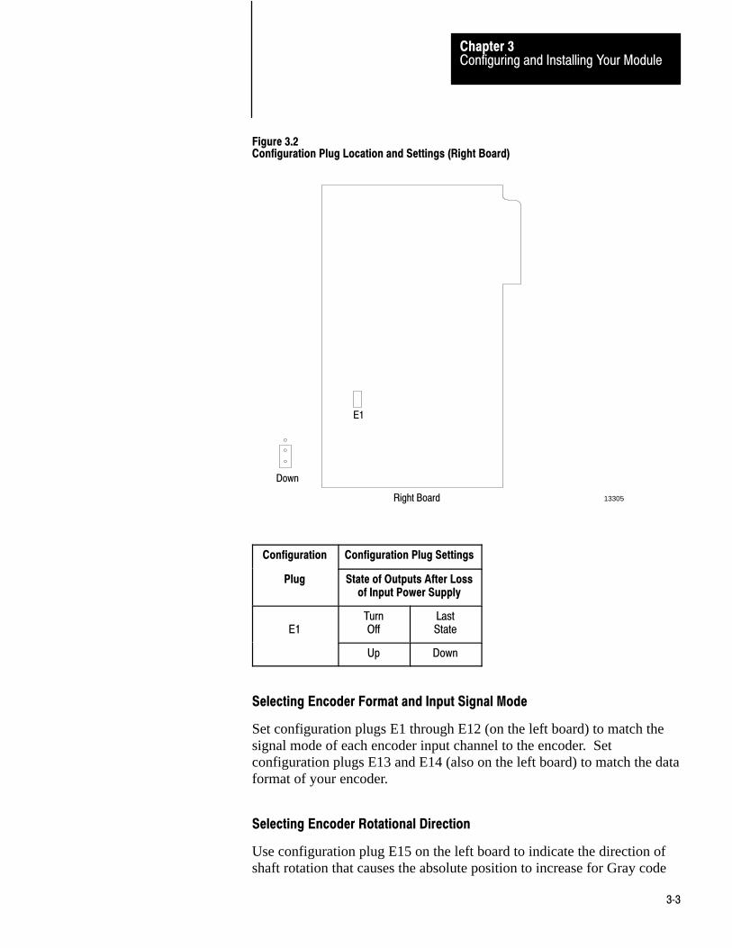
Figure 3.2Configuration Plug Location and Settings (Right Board)
E1
Right Board 13305
Down
Configuration Configuration Plug Settings
Plug State of Outputs After Lossof Input Power Supply
E1TurnOff
LastState
Up Down
Selecting Encoder Format and Input Signal Mode
Set configuration plugs E1 through E12 (on the left board) to match thesignal mode of each encoder input channel to the encoder. Setconfiguration plugs E13 and E14 (also on the left board) to match the dataformat of your encoder.
Selecting Encoder Rotational Direction
Use configuration plug E15 on the left board to indicate the direction ofshaft rotation that causes the absolute position to increase for Gray code
Configuring and Installing Your ModuleChapter 3
3�4
encoders. This is the same as selecting “high true” or “low true” inputsfrom the Gray encoder.
Configuration plug E15 is factory-set in the right position. It gives anincreased count when the encoder rotates clockwise when looking at theshaft. If your encoder shows a decreased count, change the plug to theleft position.
If your Grayencoder has:
and E15 is inthis position
the encodershows:
12 bits right an increased count
left a decreased count
less than 12 bits right an increased count
left a decreased count starting with 4,095
This configuration plug does not affect BCD or binary encoders.
Selecting State of Outputs Upon Loss of Input Power
Use configuration plug E1 on the right board to choose the state of theoutputs if the module loses input power. The plug is factory-set for theoutputs to turn off if input power is lost (up position). If you want theoutputs to remain in their state at loss of input power, set the plug to thedown position.
Except for downloading programs or commands and reporting status, themodule operates independent of the host processor. In the event of aprocessor or I/O communications fault, the module either continuesoperation or its outputs turn off, depending on how you set the last stateswitch of the chassis in which you place the module.
If you set the last state switch to turn outputs off, the module’s outputs areturned off.
If you set the last state switch to hold outputs in last state, the modulecontinues operating.
Plastic keying bands are shipped with each I/O chassis. These bandsensure that only a selected type of module can be placed in a particular
Response to External Fault
Keying
Configuring and Installing Your ModuleChapter 3
3�5
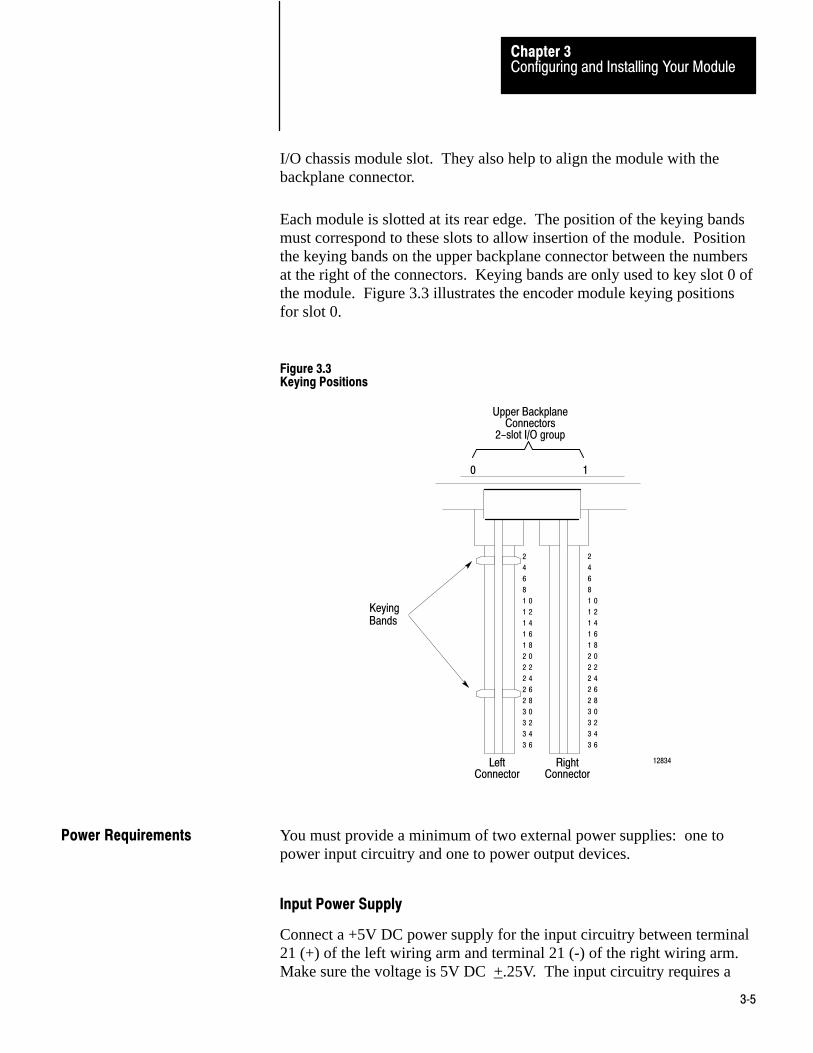
I/O chassis module slot. They also help to align the module with thebackplane connector.
Each module is slotted at its rear edge. The position of the keying bandsmust correspond to these slots to allow insertion of the module. Positionthe keying bands on the upper backplane connector between the numbersat the right of the connectors. Keying bands are only used to key slot 0 ofthe module. Figure 3.3 illustrates the encoder module keying positionsfor slot 0.
Figure 3.3Keying Positions
2
4
6
8
1 0
1 2
1 4
1 6
1 8
2 0
2 2
2 4
2 6
2 8
3 0
3 2
3 4
3 6
2
4
6
8
1 0
1 2
1 4
1 6
1 8
2 0
2 2
2 4
2 6
2 8
3 0
3 2
3 4
3 6
KeyingBands
12834LeftConnector
RightConnector
0 1
Upper BackplaneConnectors
2-slot I/O group
You must provide a minimum of two external power supplies: one topower input circuitry and one to power output devices.
Input Power Supply
Connect a +5V DC power supply for the input circuitry between terminal21 (+) of the left wiring arm and terminal 21 (-) of the right wiring arm.Make sure the voltage is 5V DC +.25V. The input circuitry requires a
Power Requirements
Configuring and Installing Your ModuleChapter 3
3�6
maximum of 300mA.
For the best system noise immunity, we recommend use of a separate,linear regulated power supply for powering the input circuitry and theencoder. You can use this supply for more than one absolute encodermodule or encoder, but do not use it for otehr 5V loads such as relays.Make sure the power supply has enough additional current capacity forthe encoder.
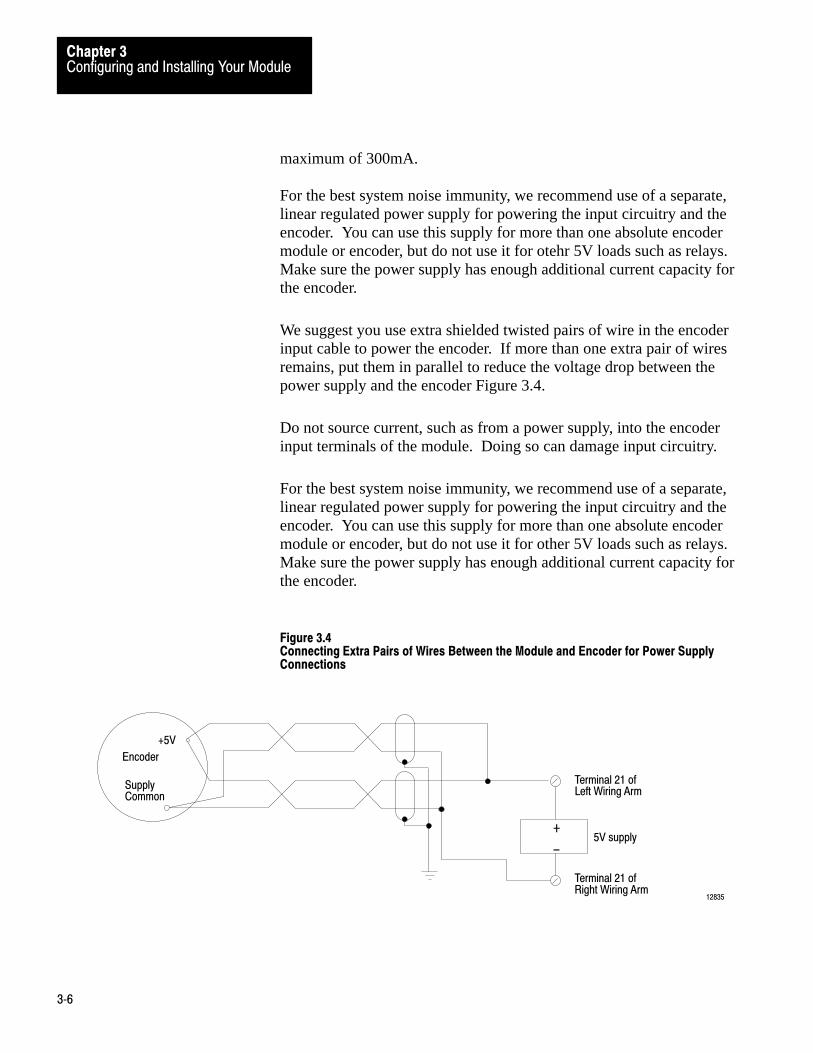
We suggest you use extra shielded twisted pairs of wire in the encoderinput cable to power the encoder. If more than one extra pair of wiresremains, put them in parallel to reduce the voltage drop between thepower supply and the encoder Figure 3.4.
Do not source current, such as from a power supply, into the encoderinput terminals of the module. Doing so can damage input circuitry.
For the best system noise immunity, we recommend use of a separate,linear regulated power supply for powering the input circuitry and theencoder. You can use this supply for more than one absolute encodermodule or encoder, but do not use it for other 5V loads such as relays.Make sure the power supply has enough additional current capacity forthe encoder.
Figure 3.4Connecting Extra Pairs of Wires Between the Module and Encoder for Power SupplyConnections
+
-5V supply
Terminal 21 ofLeft Wiring Arm
Terminal 21 ofRight Wiring Arm
+5V
Encoder
Supply Common
12835
Configuring and Installing Your ModuleChapter 3
3�7
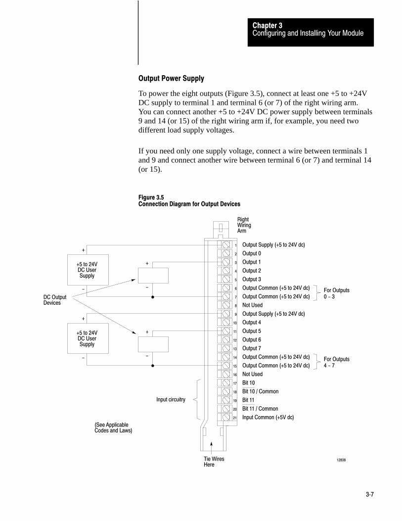
Output Power Supply
To power the eight outputs (Figure 3.5), connect at least one +5 to +24VDC supply to terminal 1 and terminal 6 (or 7) of the right wiring arm.You can connect another +5 to +24V DC power supply between terminals9 and 14 (or 15) of the right wiring arm if, for example, you need twodifferent load supply voltages.
If you need only one supply voltage, connect a wire between terminals 1and 9 and connect another wire between terminal 6 (or 7) and terminal 14(or 15).
Figure 3.5Connection Diagram for Output Devices
1
2
3
4
5
6
7
8
9
10
11
12
13
14
15
16
17
18
19
20
21
Output Supply (+5 to 24V dc)
Output 0
Output 1
Output 2
Output 3
Output Common (+5 to 24V dc)
Output Common (+5 to 24V dc)
Not Used
Output Supply (+5 to 24V dc)
Output 4
Output 5
Output 6
Output 7
Output Common (+5 to 24V dc)
Output Common (+5 to 24V dc)
Not Used
Bit 10
Bit 10 / Common
Bit 11
Bit 11 / Common
Input Common (+5V dc)
12838
RightWiringArm
For Outputs0 - 3
For Outputs4 - 7
+5 to 24VDC UserSupply
+
-
+
-
+5 to 24VDC UserSupply
+
-
+
-
DC OutputDevices
Input circuitry
Tie WiresHere
(See ApplicableCodes and Laws)
Configuring and Installing Your ModuleChapter 3
3�8
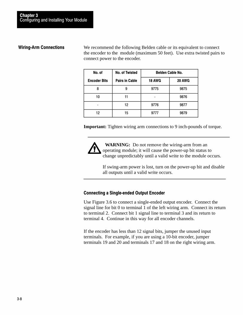
We recommend the following Belden cable or its equivalent to connectthe encoder to the module (maximum 50 feet). Use extra twisted pairs toconnect power to the encoder.
No. of No. of Twisted Belden Cable No.
Encoder Bits Pairs in Cable 18 AWG 20 AWG
8 9 9775 9875
10 11 � 9876
� 12 9776 9877
12 15 9777 9879
Important: Tighten wiring arm connections to 9 inch-pounds of torque.
WARNING: Do not remove the wiring-arm from anoperating module; it will cause the power-up bit status tochange unpredictably until a valid write to the module occurs.
If swing-arm power is lost, turn on the power-up bit and disableall outputs until a valid write occurs.
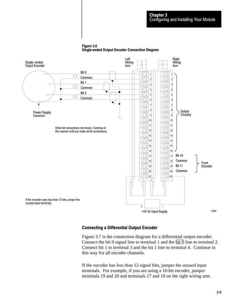
Connecting a Single�ended Output Encoder
Use Figure 3.6 to connect a single-ended output encoder. Connect thesignal line for bit 0 to terminal 1 of the left wiring arm. Connect its returnto terminal 2. Connect bit 1 signal line to terminal 3 and its return toterminal 4. Continue in this way for all encoder channels.
If the encoder has less than 12 signal bits, jumper the unused inputterminals. For example, if you are using a 10-bit encoder, jumperterminals 19 and 20 and terminals 17 and 18 on the right wiring arm.
Wiring�Arm Connections
Configuring and Installing Your ModuleChapter 3
3�9
Figure 3.6Single�ended Output Encoder Connection Diagram
1
2
3
4
5
6
7
8
9
10
11
12
13
14
15
16
17
18
19
20
21
1
2
3
4
5
6
7
8
9
10
11
12
13
14
15
16
17
18
19
20
21
Bit 10
Common
Bit 11
Common
12836
LeftWiringArm
RightWiringArm
FromEncoder
+5V dc Input Supply
+ -
Power SupplyCommon
Single-endedOuput Encoder
Bit 0
Common
Bit 1
Common
Bit 2
Common
Other bit connections not shown. Continue in this manner until you make all bit connections.
OutputCircuitry
If the encoder uses less than 12 bits, jumper theunused input terminals.
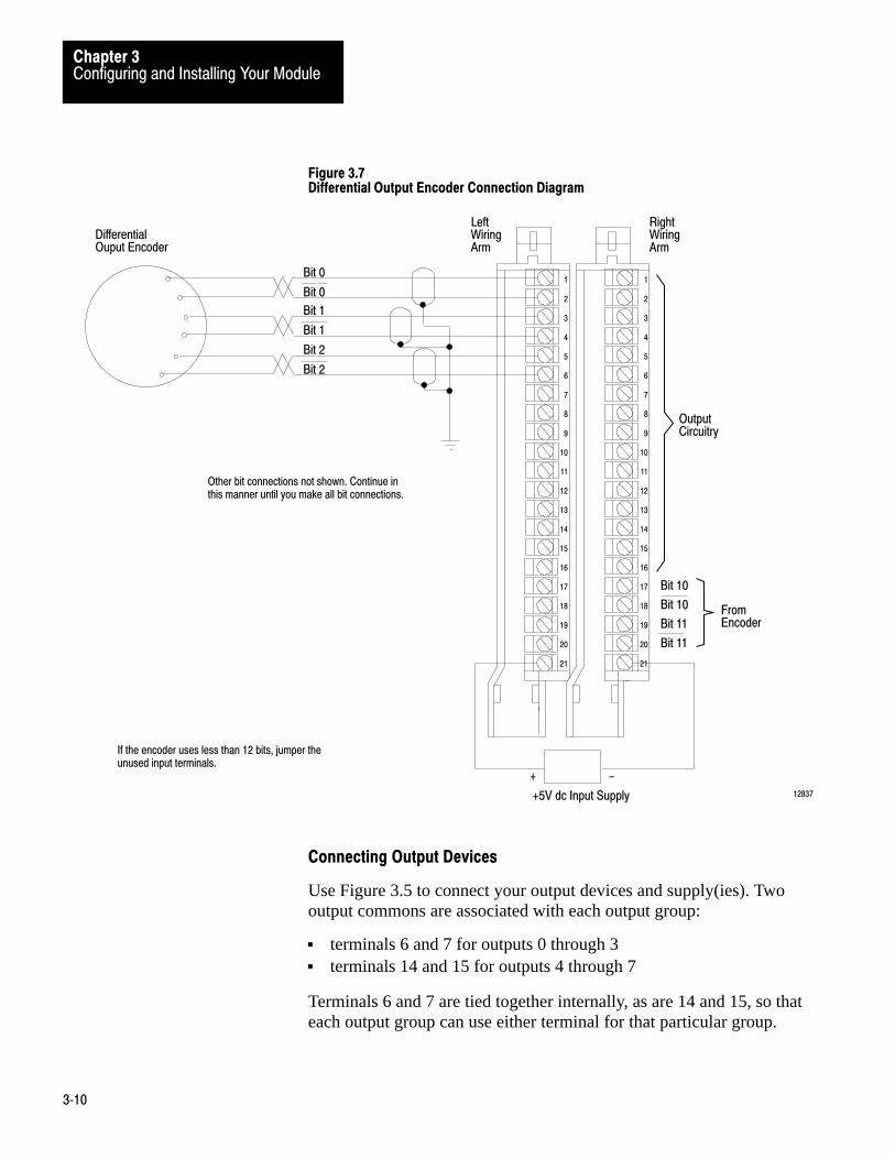
Connecting a Differential Output Encoder
Figure 3.7 is the connection diagram for a differential output encoder.Connect the bit 0 signal line to terminal 1 and the bit 0 line to terminal 2.Connect bit 1 to terminal 3 and the bit 1 line to terminal 4. Continue inthis way for all encoder channels.
If the encoder has less than 12 signal bits, jumper the unused inputterminals. For example, if you are using a 10-bit encoder, jumperterminals 19 and 20 and terminals 17 and 18 on the right wiring arm.
Configuring and Installing Your ModuleChapter 3
3�10
Figure 3.7Differential Output Encoder Connection Diagram
1
2
3
4
5
6
7
8
9
10
11
12
13
14
15
16
17
18
19
20
21
1
2
3
4
5
6
7
8
9
10
11
12
13
14
15
16
17
18
19
20
21
Bit 10
Bit 10
Bit 11
Bit 11
12837
LeftWiringArm
RightWiringArm
FromEncoder
+5V dc Input Supply
+ -
DifferentialOuput Encoder
Bit 0
Bit 0
Bit 1
Bit 1
Bit 2
Bit 2
Other bit connections not shown. Continue in this manner until you make all bit connections.
OutputCircuitry
If the encoder uses less than 12 bits, jumper theunused input terminals.
Connecting Output Devices
Use Figure 3.5 to connect your output devices and supply(ies). Twooutput commons are associated with each output group:
terminals 6 and 7 for outputs 0 through 3 terminals 14 and 15 for outputs 4 through 7
Terminals 6 and 7 are tied together internally, as are 14 and 15, so thateach output group can use either terminal for that particular group.
Configuring and Installing Your ModuleChapter 3
3�11
Now that you’ve determined the power requirements, keying, and wiringfor your module, you can use the following procedure to install it.
Refer to the Programmable Controller Grounding and Wiring Guidelines(pub. no. 1770-4.1) for proper grounding and wiring methods to installyour module.
WARNING: Remove power from the 1771 I/O chassisbackplane and wiring arm before installing or removing themodule.
Failure to remove power from the backplane or wiring arm could causemodule damage, degradation of performance, or injury.
Failure to remove power from the backplane could cause injury and/orequipment damage due to possible unexpected operation.
WARNING: Install the module in the I/O chassis so that bothhalves of the module are in the same I/O group. Failure toobserve this rule will result in faulty module operation and/ordamage to the module circuitry with possible injury topersonnel.
CAUTION: Do not force the module into a backplaneconnector. If you can’t seat it with firm pressure, check thealignment and keying. You can damage the connector or themodule if you force it into the connector.
1. Remove power from the I/O chassis before inserting (or removing)the module.
2. Open the module locking latch on the I/O chassis and insert themodule into the slot keyed for it.
3. Firmly press to seat the module into its backplane connector.
4. Secure the module with the module locking latch.
Installing the Module

Configuring and Installing Your ModuleChapter 3
3�12
This chapter told you how to select features and set configuration plugs onthe absolute encoder module, and described the power requirements,keying, wiring, and installation of the module. In the next chapter youwill read about block-transfer file parameters.
Summary

Chapter
4
4�1
Module/Processor Communication
This chapter describes file parameters for the block-transfer data files youuse to write data to and read data from the absolute encoder module.
The absolute encoder module and the processor communicate throughblock-transfer programming. Processors that use block-transferprogramming are listed below, along with the respective programmingmanual. Refer to the latest edition of the programming manual for adetailed description of block transfer.
Processor Programming and OperationsManual Publication Number
Mini�PLC�2 1772�6.8.4
Mini�PLC�2/15 1772�6.8.2
Mini�PLC�2/05 1772�6.8.6
PLC�2/20 1772�6.8.1
PLC�2/30 1772�6.8.3
PLC�3 1772�6.4.1
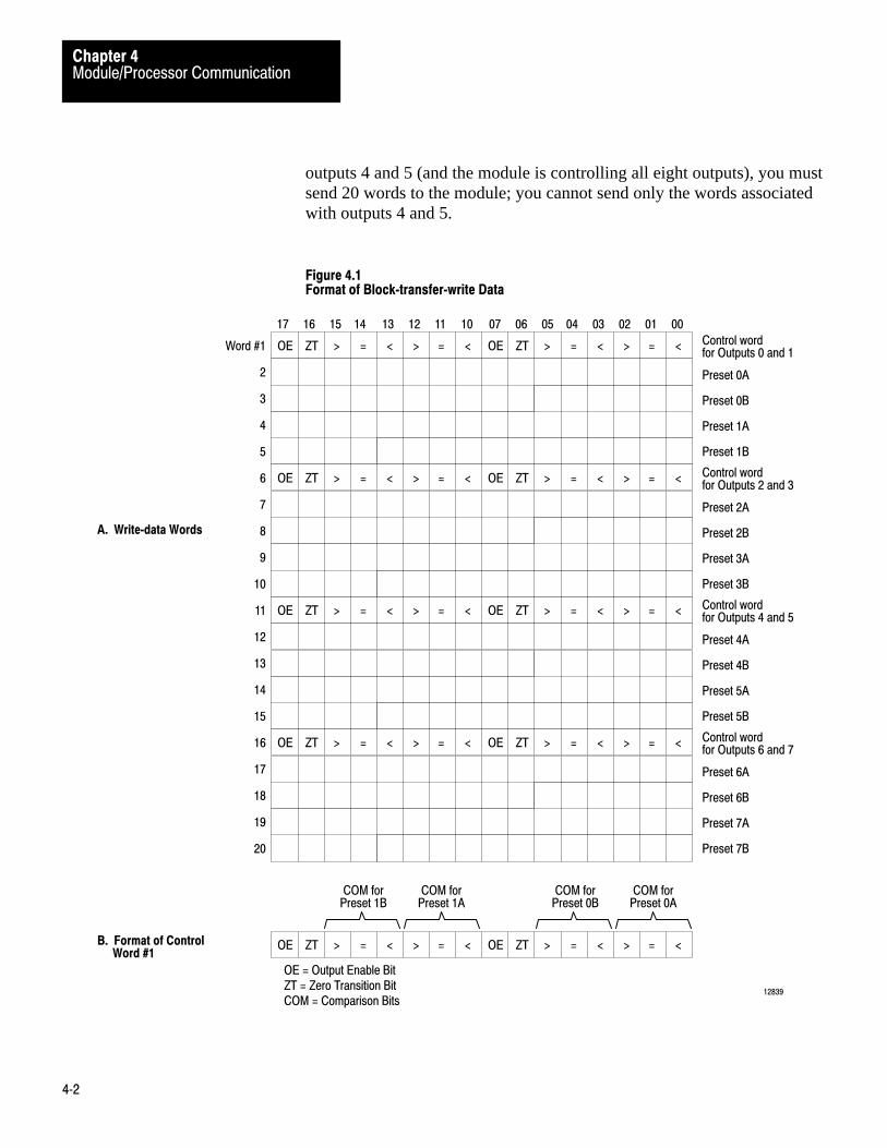
You write data to the module in blocks. You can write 5, 10, 15 or 20words in one block-transfer operation. Each block of five words isassociated with two outputs and is identical to each other in format:
words 1-5 - outputs 0 and 1words 6-10 - outputs 2 and 3words 11-15 - outputs 4 and 5words 16-20 - outputs 6 and 7
The first word of each block is a control word. The last four words arepreset words. The formats of the write-data words and control word 1 areshown in Figure 4.1 and are described here.
You can send a maximum of 20 words (four block of five words) in oneblock-transfer operation. The number of words you send to the moduledetermines how many outputs it controls. If you want to change data for
Chapter Objectives
Block Transfer
Block�transfer�write Data
Module/Processor CommunicationChapter 4
4�2
outputs 4 and 5 (and the module is controlling all eight outputs), you mustsend 20 words to the module; you cannot send only the words associatedwith outputs 4 and 5.
Figure 4.1Format of Block�transfer�write Data
17 16 15 14 13 12 11 10 07 06 05 04 03 02 01 00
OE ZT > = < > = < OE ZT > = < > = < Control wordfor Outputs 0 and 1
Preset 0A
Preset 0B
Preset 1A
Preset 1B
Word #1
2
3
4
5
OE ZT > = < > = < OE ZT > = < > = < Control wordfor Outputs 2 and 3
Preset 2A
Preset 2B
Preset 3A
Preset 3B
6
7
8
9
10
OE ZT > = < > = < OE ZT > = < > = < Control wordfor Outputs 4 and 5
Preset 4A
Preset 4B
Preset 5A
Preset 5B
11
12
13
14
15
OE ZT > = < > = < OE ZT > = < > = < Control wordfor Outputs 6 and 7
Preset 6A
Preset 6B
Preset 7A
Preset 7B
16
17
18
19
20
A. Write�data Words
OE ZT > = < > = < OE ZT > = < > = <
OE = Output Enable BitZT = Zero Transition BitCOM = Comparison Bits
COM forPreset 1B
COM forPreset 1A
COM forPreset 0B
COM forPreset 0A
B. Format of ControlWord #1
12839
Module/Processor CommunicationChapter 4
4�3
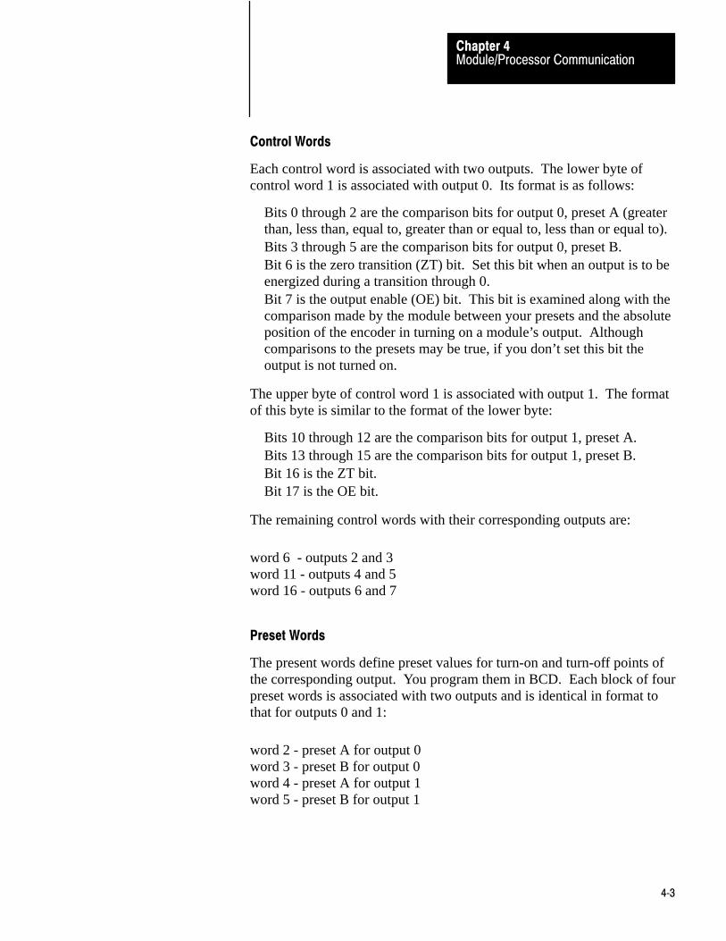
Control Words
Each control word is associated with two outputs. The lower byte ofcontrol word 1 is associated with output 0. Its format is as follows:
Bits 0 through 2 are the comparison bits for output 0, preset A (greaterthan, less than, equal to, greater than or equal to, less than or equal to).Bits 3 through 5 are the comparison bits for output 0, preset B.Bit 6 is the zero transition (ZT) bit. Set this bit when an output is to beenergized during a transition through 0.Bit 7 is the output enable (OE) bit. This bit is examined along with thecomparison made by the module between your presets and the absoluteposition of the encoder in turning on a module’s output. Althoughcomparisons to the presets may be true, if you don’t set this bit theoutput is not turned on.
The upper byte of control word 1 is associated with output 1. The formatof this byte is similar to the format of the lower byte:
Bits 10 through 12 are the comparison bits for output 1, preset A.Bits 13 through 15 are the comparison bits for output 1, preset B.Bit 16 is the ZT bit.Bit 17 is the OE bit.
The remaining control words with their corresponding outputs are:
word 6 - outputs 2 and 3word 11 - outputs 4 and 5word 16 - outputs 6 and 7
Preset Words
The present words define preset values for turn-on and turn-off points ofthe corresponding output. You program them in BCD. Each block of fourpreset words is associated with two outputs and is identical in format tothat for outputs 0 and 1:
word 2 - preset A for output 0word 3 - preset B for output 0word 4 - preset A for output 1word 5 - preset B for output 1
Module/Processor CommunicationChapter 4
4�4
Thewrite-data throughput time is the time between the end of ablock-transfer-write operation and the module update of its outputs. Themodule’s response time can vary, depending on the number of outputs itcontrols, the type of absolute encoder you use, and if you have an offsetvalue. The worst case is 4.7 ms. Use the following table to determine themodule’s response time in milliseconds for your application.
Type of Encoder (with or without offset)
BCD without offset 2 4 6 8
BCD with offset Gray code or binary without offsetGray code or binary with offset
1.22.01.31.9
1.82.92.02.6
2.53.82.63.4
3.14.73.34.1
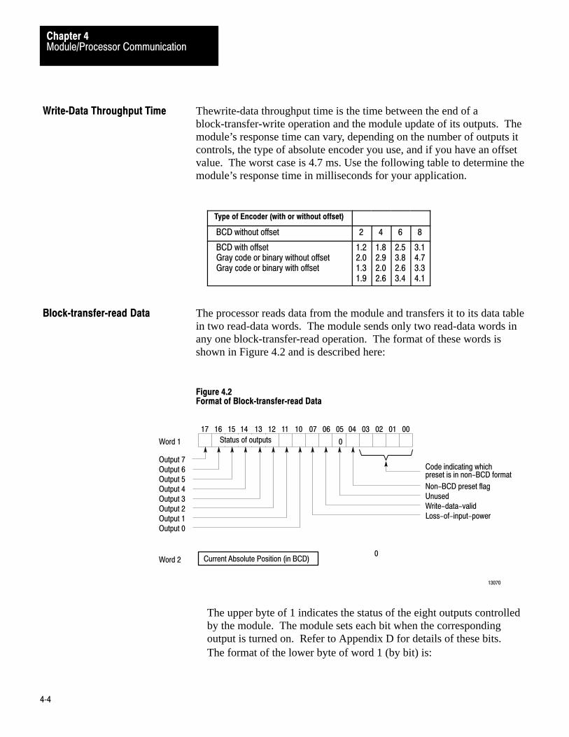
The processor reads data from the module and transfers it to its data tablein two read-data words. The module sends only two read-data words inany one block-transfer-read operation. The format of these words isshown in Figure 4.2 and is described here:
Figure 4.2Format of Block�transfer�read Data
17 16 15 14 13 12 11 10 07 06 05 04 03 02 01 00
0
Output 7Output 6Output 5Output 4Output 3Output 2Output 1Output 0
Code indicating whichpreset is in non-BCD format
Non-BCD preset flagUnusedWrite-data-validLoss-of-input-power
Word 1
Word 2
Status of outputs
13070
Current Absolute Position (in BCD)0
The upper byte of 1 indicates the status of the eight outputs controlledby the module. The module sets each bit when the correspondingoutput is turned on. Refer to Appendix D for details of these bits.The format of the lower byte of word 1 (by bit) is:
Write�Data Throughput Time
Block�transfer�read Data
Module/Processor CommunicationChapter 4
4�5
Bit 7 is the loss-of-input-power bit. It is set when input power islost; it is reset when power is restored and bit 6 is reset.
Bit 6 is the write-data-valid bit. It is set at power-up and when theprocessor changes from the program mode to the run mode; it is resetwhen the module receives valid data in a block-transfer-writeoperation.
Bit 5 is unused. Bit 4 is the non-BCD preset flag. It is set when any preset is innon-BCD format.
Bits 3 through 0 are a binary or hexadecimal code that indicates whichpreset is not in BCD format. (Refer to Appendix D for the value ofthese bits.) The module identifies each incorrect preset in the orderit finds them (one at a time). Once you correct a preset, the modulecontinues to identify any non-BCD preset.
Word 2 indicates the current absolute position of the encoder in BCD.
Presets are interpreted by the module as absolute numbers to be comparedto the absolute position of the encoder shaft; they are not interpreted asdegrees of shaft rotation.
Thus, if you have a 0 to 999-position encoder, you program presets foroutput 3, for example, as:
Preset 3A = 200Preset 3B = 402
There is no restriction on which mode of comparison you can use forpreset A or preset B.
In this example, we assume the use of a 0 to 359-position encoder whenreferring to degrees of shaft rotation.
If you want to turn on output 0 between shaft positions 330 (preset A) and005 (preset B), you set:
the “greater than” and “equal to” bits for preset Athe “less than” and “equal to” bits for preset Bthe ZT bit
Programming Example

Module/Processor CommunicationChapter 4
4�6
the OE bit
Output 0 is turned on when the shaft position is greater than or equal to 330 or when the shaft position is less than or equal to 005.
If you don’t set the ZT bit in the above control word, when the encodershaft position is 002, for example, comparison B is true, comparison A isnot true, and the output is turned off. (At position 002, the shaft positionis less than or equal to 005, but it is not greater than or equal to 330.) Youmust set the ZT bit when an output is to be energized during a transitionthrough 0.
Another way to energize output 0 between position 330 and 005 is to givepreset A a value of 006 and preset B a value of 329. Then you set:
the “less than” bit for preset Athe “greater than” bit for preset Bthe ZT bitOE bit
In either case, you must set bit 6 (ZT) to indicate that the output should beon if either comparison A or comparison B is true.
Let’s continue this example and assume your application requirements foroutputs 0 and 1 are:
output 0 is to turn on at position 330 and turn off at position 005output 1 is to turn on between position 007 and position 011
Once you define the presets for outputs 0 and 1, determine the comparisonbits for each preset, and enter the data into the data file, the block of datayou write to the module (five words) looks like this:
17 16 15 14 13 12 11 10 07 06 05 04 03 02 01 00
OE ZT > = < > = < OE ZT > = < > = <
0
0
0
0
3
0
0
0
3
0
0
1
0
5
7
1
Bit #
ControlWordFunction
ControlWord
Preset 0A
Preset 0B
Preset 1A
Preset 1B
binary
BCD
digits
1 0 0 0 1 1 0 0 1 1 0 1 1 1 1 0

Module/Processor CommunicationChapter 4
4�7
When you specify the default block length (00), the followingconsiderations apply for PLC-2 family processors:
You can and should enable the read and write instructions in the samescan (separate but equal input conditions).
The module decides which operation is performed first when bothinstructions are enabled in the same scan.
Alternate operation is performed in a subsequent scan.
Do not operate on transferred data until the done bit is set.
When you examine the read and write files, 64 words appear to be moved;however, the processor writes only 20 words and reads only two words inany block-transfer operation.
WARNING: When the block lengths of bidirectionalblock-transfer instructions are set to unequal values, do notenable the rung containing the alternate instruction until thedone bit of the first transfer is set. If you enable them in thesame scan, the number of words transferred may not be thenumber intended, invalid data could be operated upon insubsequent scans, or output devices could be controlled byinvalid data. Unexpected and/or hazardous machine operationcould occur. Damage to equipment and/or personal injury couldresult.
This chapter gave a description of the file parameters for programmingblock-transfer-read and -write operations for the absolute encoder module.It also gave several programming examples and considerations for usewith the absolute encoder module. The next chapter describestroubleshooting the module.
Programming Considerations
Summary
Chapter
5
5�1
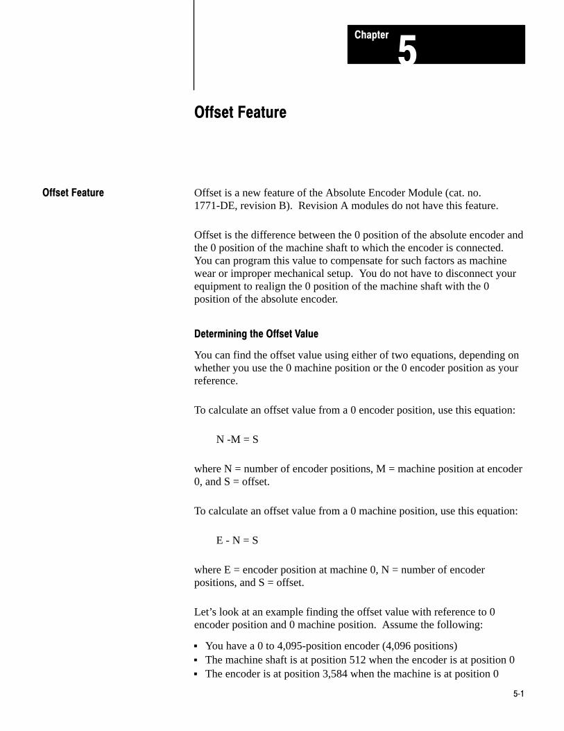
Offset Feature
Offset is a new feature of the Absolute Encoder Module (cat. no.1771-DE, revision B). Revision A modules do not have this feature.
Offset is the difference between the 0 position of the absolute encoder andthe 0 position of the machine shaft to which the encoder is connected.You can program this value to compensate for such factors as machinewear or improper mechanical setup. You do not have to disconnect yourequipment to realign the 0 position of the machine shaft with the 0position of the absolute encoder.
Determining the Offset Value
You can find the offset value using either of two equations, depending onwhether you use the 0 machine position or the 0 encoder position as yourreference.
To calculate an offset value from a 0 encoder position, use this equation:
N -M = S
where N = number of encoder positions, M = machine position at encoder0, and S = offset.
To calculate an offset value from a 0 machine position, use this equation:
E - N = S
where E = encoder position at machine 0, N = number of encoderpositions, and S = offset.
Let’s look at an example finding the offset value with reference to 0encoder position and 0 machine position. Assume the following:
You have a 0 to 4,095-position encoder (4,096 positions) The machine shaft is at position 512 when the encoder is at position 0 The encoder is at position 3,584 when the machine is at position 0
Offset Feature
Offset ProgrammingChapter 5
5�2
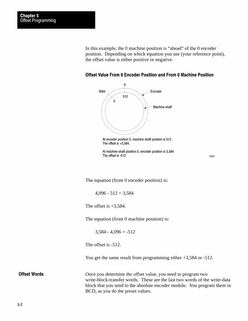
In this example, the 0 machine position is “ahead” of the 0 encoderposition. Depending on which equation you use (your reference point),the offset value is either positive or negative.
Offset Value From 0 Encoder Position and From 0 Machine Position
3584
0
0
512
Encoder
Machine shaft
At encoder position 0, machine shaft position is 512.The offset is +3,584.
At machine shaft position 0, encoder position is 3,584.The offset is �512. 13522
The equation (from 0 encoder position) is:
4,096 - 512 = 3,584
The offset is +3,584.
The equation (from 0 machine position) is:
3,584 - 4,096 = -512
The offset is -512.
You get the same result from programming either +3,584 or -512.
Once you determine the offset value, you need to program twowrite-block-transfer words. These are the last two words of the write-datablock that you send to the absolute encoder module. You program them inBCD, as you do the preset values.
Offset Words

Offset ProgrammingChapter 5
5�3
Format of Offset Words
517 16 15 14 13 12 11 10 7 6 4 3 2 1 0
S OFFSET VALUE
NO. OF ENCODER POSITIONS
The offset words are the last two words of the write-data block that you sendto the absolute encoder module.
If you are controlling
2 outputs4 outputs6 outputs8 outputs
The offset words are:
words 6 and 7words 11 and 12words 16 and 17words 21 and 22
S = sign bit. Set this bit if the offset has a negative value; reset the bit if the offset has a positive value.
Bit #
13523
The first offset word contains the value of the offset. Bit 17 of this wordis the sign bit. It indicates whether the offset is negative or positive. Setbit 17 if the offset is negative; reset it if the offset is positive.
The second offset word is the number of positions of the encoder. If youare using a 0 to 4,095-position encoder, your second offset word is 4,096.
Block�transfer�write Data with Offset
The number of words you send to the module depends on the number ofoutputs the module controls. The offset feature adds two words to thetotal number of words you send to the module:
If the modulecontrols:
You send:
2 outputs 7 words
4 outputs 12 words
6 outputs 17 words
8 outputs 22 words
If the module is controlling eight outputs, your block-transfer-write datanow looks like this:

Offset ProgrammingChapter 5
5�4
Figure 5.1Format of Block�transfer�write Data with Offset
17 16 15 14 13 12 11 10 07 06 05 04 03 02 01 00
OE ZT <Word #1 > = <> = OE ZT <> = <> = Control Word forOutputs 0 and 1
2 Preset 0A
3 Preset 0B
4 Preset 1A
5 Preset 1B
OE ZT <6 > = <> = OE ZT <> = <> = Control Word forOutputs 2 and 3
7 Preset 2A
8 Preset 2B
9 Preset 3A
10 Preset 3B
OE ZT <11 > = <> = OE ZT <> = <> = Control Word forOutputs 4 and 5
12 Preset 4A
13 Preset 4B
14 Preset 5A
15 Preset 5B
OE ZT <16 > = <> = OE ZT <> = <> = Control Word forOutputs 6 and 7
17 Preset 6A
18 Preset 6B
19 Preset 7A
20 Preset 7B
21 Offset Value
22 No. of Encoder Positions
S
A. Write-data words
B. Format of control word #1
OE ZT <> = <> = OE ZT <> = <> =
COM forPreset 1B
COM forPreset 1A
COM forPreset 0B
COM forPreset 0A
OE = Output Enable Bit
ZT = Zero Transition BitCOM = Comparison BitS = Offset Sign Bit
10698�I
Block�transfer�read Data with Offset
The upper byte of word 1 indicates the status of the eight outputscontrolled by the module. The module sets each bit when thecorresponding output is turned on.
The lower byte of word 1 (by bit) is:
Offset ProgrammingChapter 5
5�5
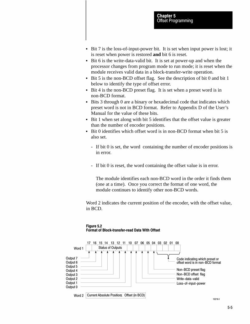
Bit 7 is the loss-of-input-power bit. It is set when input power is lost; itis reset when power is restored and bit 6 is reset.
Bit 6 is the write-data-valid bit. It is set at power-up and when theprocessor changes from program mode to run mode; it is reset when themodule receives valid data in a block-transfer-write operation.
Bit 5 is the non-BCD offset flag. See the description of bit 0 and bit 1below to identify the type of offset error.
Bit 4 is the non-BCD preset flag. It is set when a preset word is innon-BCD format.
Bits 3 through 0 are a binary or hexadecimal code that indicates whichpreset word is not in BCD format. Refer to Appendix D of the User’sManual for the value of these bits.
Bit 1 when set along with bit 5 identifies that the offset value is greaterthan the number of encoder positions.
Bit 0 identifies which offset word is in non-BCD format when bit 5 isalso set.
- If bit 0 is set, the word containing the number of encoder positions isin error.
- If bit 0 is reset, the word containing the offset value is in error.
The module identifies each non-BCD word in the order it finds them(one at a time). Once you correct the format of one word, themodule continues to identify other non-BCD words.
Word 2 indicates the current position of the encoder, with the offset value,in BCD.
Figure 5.2Format of Block�transfer�read Data With Offset
17 16 15 14 13 12 11 10 07 06 05 04 03 02 01 00
Status of Outputs
Output 7Output 6Output 5Output 4Output 3Output 2Output 1Output 0
Code indicating which preset oroffset word is in non-BCD format
Non-BCD preset flagNon-BCD offset flagWrite-data-validLoss-of-input-power
Word 1
Word 2 Current Absolute Position + Offset (in BCD)10216�I
Offset ProgrammingChapter 5
5�6
The default block lengths (00) for block-transfer instructions are 20block-transfer-write words and two block-transfer-read words. These arethe block lengths that transfer to and from the absolute encoder regardlessof whether you use the offset feature.
When you have an offset value and the module is controlling eightoutputs, for example, the number of words you send to the module is 22.You must enter the numbers 22 and 2 for the block lengths of write andread data. Do not enter the default block length in your instructions if youuse the module’s offset feature.
For PLC-2 family processors, do not enable the read- andwrite-block-transfers in the same scan when you use the offset feature.An example program enabling the instructions in separate scans follows.
WARNING: When the block lengths of bidirectionalblock-transfer instructions are set to unequal values, do notenable the rung containing the alternate instruction until thedone bit of the first transfer is set. If you enable them in thesame scan:
the number of words transferred may not be the numberintended
invalid data could be operated upon in subsequent scans output devices could be controlled by invalid data
Unexpected and or hazardous machine operation could occur.Damage to equipment and/or injury could result.
Programming Considerationswith Offset
Offset ProgrammingChapter 5
5�7
ENBLOCK XFER READ
DATA ADDR:MODULE ADDR:BLOCK LENGTH:FILE:
0040220
020200 - 0201
DN
ENFILE TO FILE MOVECOUNTER ADDR:POSITION:FILE LENGTH:FILE A:
0044001002
0200-0201
DNFILE R:RATE PER SCAN
0226-0227002
200
06
L
200
04121
00
122
06
200
04
U
077
OFF00
077
OFF00
| | | |022 122
06 07
022
07
122
07
READ FILEDONEBIT
122
DONEBIT
044
07 15
0044
17
0044
15
ENBLOCK XFER READ
DATA ADDR:MODULE ADDR:BLOCK LENGTH:FILE:
0041220
220202 - 0227
DN
ENFILE TO FILE MOVECOUNTER ADDR:POSITION:FILE LENGTH:FILE A:
0043001022
0202-0227
DNFILE R:RATE PER SCAN
0200-0225022
022
06
122
06
0043
17
0043
15
077
00
| | | |022 122
07 06
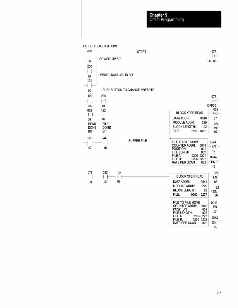
LADDER DIAGRAM DUMP
START
POWER-UP BIT
WRITE-DATA-VALID BIT
PUSHBUTTON TO CHANGE PRESETS
BUFFER FILE

Offset ProgrammingChapter 5
5�8
Rung 1 200/06 and 200/04 are returned in the read operation and latch077/00. When 077/00 is latched, the module toggles between aread operation and a write operation.
121/00 is optional and lets the processor initiate ablock�transfer�write operation.
Rung 2 This rung examines the write�done�bit (122/06) and the validBCD data bit (200/04) to unlatch 077/00 and begin theread�only operation.
Rung 3 This rung contains the block�transfer�read instruction,conditioned by the read done bit and the write enable bit.
Rung 4 Use a file�to�file move to buffer the read data. Use addresses0226 and 0227 when making any data comparisons.
Rung 5 This rung contains the block�transfer�write instruction,conditioned by the write done bit and the read enable bit.
Rung 6 This rung is for display purposes only.

Chapter
6
6�1
Troubleshooting
In this chapter you will read how to troubleshoot your absolute encodermodule using the ACTIVE (GREEN) and FAULT (red) indicators,block-transfer rungs in your ladder program, and diagnostic bits in word 2of the read-data file.
The following table lists problems indicated by LED changes, possiblecauses, and recomended actions.
LED = ON LED = OFF
Indication Description Recommended Action
ACTIVE
FAULT
Normal operation; module should operatewhen the PC goes into the RUN mode andyou send presets.
None
ACTIVE
FAULT
Module is held reset at power�up; probablemalfunction in adapter module or processormodule.
Substitute adapter module, power supply, orprocessor module.
ACTIVEFAULT
Module has detected a hardware fault in itspower�up diagnostic routine.
Return module for repair.
ACTIVEFAULT
Module is not receiving DC power from thechassis backplane.
Check chassis power supply (ies).
Observe the block-transfer rungs in your ladder diagram program. Youhave a block-transfer error when you observe one or both of thefollowing:
The block-transfer error bits are intensified (PLC-3 processors). The enable and done bits of block-transfer instructions do not intensify
or they remain intensified; they should alternately turn on (intensify)and turn off.
Block-transfer errors are caused if one or more of the following areincorrect:
The module’s location (rack, group, slot) in the I/O chassis must matchthe rack, group, and slot of block-transfer instructions in the ladderprogram.
Chapter Objectives
Causes of Block�transfer Errors
@@@@
TroubleshootingChapter 6
6�2
The block lengths of read- and write-block-transfer instructions shouldbe equal (PLC-2 family processors); or if they are different lengths, donot enable the read and write instruction in the same scan.
Your conditioning instructions in block-transfer rungs allow the rungsto turn off and on.
If you’re using a PLC-2/30 processor, set the scanner for block-transferoperation.
If you’re using a PLC-3 processor, create block-transfer data files.
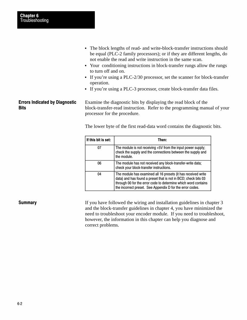
Examine the diagnostic bits by displaying the read block of theblock-transfer-read instruction. Refer to the programming manual of yourprocessor for the procedure.
The lower byte of the first read-data word contains the diagnostic bits.
If this bit is set: Then:
07 The module is not receiving +5V from the input power supply;check the supply and the connections between the supply andthe module.
06 The module has not received any block�transfer�write data;check your block�transfer instructions.
04 The module has examined all 16 presets (it has received writedata) and has found a preset that is not in BCD; check bits 03through 00 for the error code to determine which word containsthe incorrect preset. See Appendix D for the error codes.
If you have followed the wiring and installation guidelines in chapter 3and the block-transfer guidelines in chapter 4, you have minimized theneed to troubleshoot your encoder module. If you need to troubleshoot,however, the information in this chapter can help you diagnose andcorrect problems.
Errors Indicated by DiagnosticBits
Summary
Appendix
A
A�1
Block�transfer Timing
The time required for a block-transfer-read or -write operation for PLC-2family processors depends on:
the system scan time(s) the number of words to be transferred the I/O configuration the number of enabled block-transfer instructions in the ladder diagram
program during any program scan
A block-transfer module performs only one block-transfer operation perI/O scan regardless of whether both read and write operations arerequested. When done, the module toggles from one operation to theother in each program scan.
For a worst case calculation of the time between block transfers, assumethat the number of enabled block-transfer instructions during any programscan is equal to the number of block-transfer modules in the system. Alsoassume that the encoder module is transferring 20 words in a writeoperation and two words in the alternate read operation.
The method of calculating the worst case time between block transfers iscovered for the following case: PLC-2/30 remote and local systems, aPLC-3 system, and a Mini-PLC-2/l5 controller.
PLC�2/30 (PLC�2/20) Remote System
The system scan time for a remote PLC-2/30 or PLC-2/20 system is thesum of the processor scan time, the processor I/O scan time (betweenprocessor and remote distribution panel), and the remote distributionpanel I/O scan time. The remote distribution panel can process only oneblock-transfer operation per remote distribution panel scan.
You can calculate the worst case time between transfers under normaloperating conditions in three steps.
1. Calculate the system values that are determined by the systemconfiguration.
Block�transfer Timing for PLC�2Family Processors

Appendix A
A�2
Program Scan (PS) = (5 ms/1K words) x (number of programwords)
Processor I/O Scan (PIO) = (0.5 ms/rack number) x (declared racknumbers)
Remote Distribution I/O Scan (RIO) = (7 ms/chassis) x (number ofchassis)
Number of Words Transferred (W) = 20 words for one writeoperation, two words for one read operation
2. Calculate the block-transfer time for a write operation (TW) and fora read operation (TR).
TW = (PS + PIO + 2 RIO + 0.5W + 13) ms TR = (PS + PIO + 2 RIO + 0.5W +4) ms
These equations are valid for up to 10,000 cable feet between the remotedistribution panel and remote I/O chassis for a baud rate of 57.6kBd or5,000 cable feet at 115kBd.
3. Calculate the worst case system time (ST) between transfers.
ST = Sum of transfer times of all block-transfer modules in asystem taken worst case (read or write)
Example 1
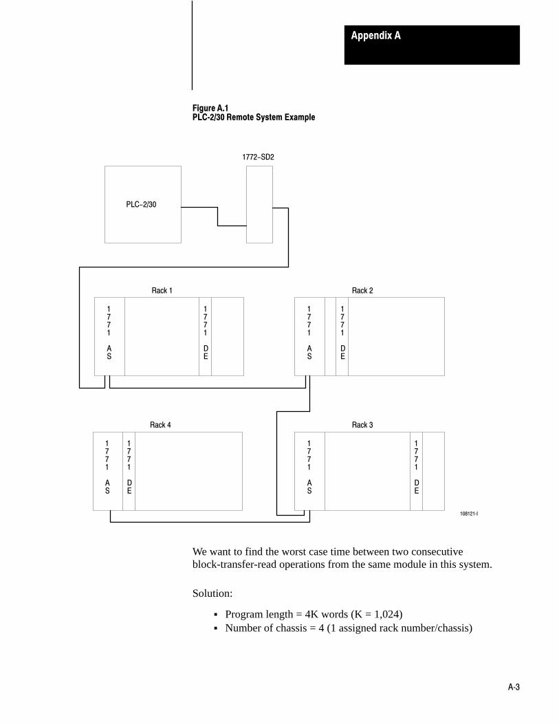
A PLC-2/30 programmable controller is controlling 4 I/O chassisin a remote configuration with 1 assigned rack number per chassis(Figure A.1). An encoder module is located in each chassis.Assume the 2 words are transferred in each read operation, 20words are transferred in each write operation, and that the ladderdiagram program contains 4K words. There are no otherblock-transfer modules in the system.
Appendix A
A�3
Figure A.1PLC�2/30 Remote System Example
PLC-2/30
1772-SD2
1771
AS
1771
DE
Rack 1
1771
AS
1771
DE
Rack 2
1771
AS
1771
DE
Rack 3
1771
AS
1771
DE
Rack 4
108121�I
We want to find the worst case time between two consecutiveblock-transfer-read operations from the same module in this system.
Solution:
Program length = 4K words (K = 1,024) Number of chassis = 4 (1 assigned rack number/chassis)
Appendix A
A�4
Number of block-transfer words = 2 words (read) or 20 words(write)
1. Calculate the system values.
Processor Scan Time (PS) = (5ms/1K words) x (4K words) = 20ms
Processor I/O Scan Time (PIO)=(0.5 ms/rack number) x (4 racknumbers) = 2 ms
Remote Distribution I/O Scan Time (RIO) = (7 mx/chassis) x (4chassis) = 28 ms
Number of Words Transferred = 2 (read) or 20 (write)
2. Calculate the block-transfer times for a write operation and for a readoperation.
TW = (PS +PIO + 2(RIO) + 0.5W + 13) ms =(20 + 2 + 2(28) + 0.5(20) + 13) ms =101 ms (write)
TR =(PS + PIO + 2(RIO) + 0.5W + 4) ms =(20 + 2 + 2(28) + 0.5(2) + 4 ms = 83 ms (read)
3. Calculate the worst case system time (ST) between 2 consecutiveblock-transfer-read operations.
ST =4TW + 4TR =4(101) + 4(83) = 736 ms
This is the worst case time between two consecutive block-transfer-readoperations in the 4-chassis remote configuration described in example 1(one enabled encoder module in each chassis).
PLC�2/30 Local System
The system scan time for a local PLC-2/30 system is the program scantime plus the processor I/O scan time. Each block-transfer module isupdated during a program scan.
The calculation of the worst case time between transfers can be done inthree steps.

Appendix A
A�5
1. Calculate the system values that are determined by the systemconfiguration.
Program Scan (PS) = (5 ms/1K words) x (number of programwords)
Processor I/O Scan (PIO) = (1 ms/rack number) x (number ofdeclared rack numbers)
Number of words transferred (W) = 2 (read) or 20 (write)
2. Calculate the block-transfer time (T) for the read or write operation.
T = 0.08 ms/word x number of words transferred
3. Calculate the worst case system time (ST) between transfers.
ST =PS + PIO + T(1)(read) + T(2)(read) +T(3)(read) +... PS + PIO + T(1)(write) + T(2)(write) + T(3)(write) +...
=2(PS + PIO) + T(1)(read) + T(2)(read) + T(3)(read) + ... T(1)(write) + T(2)(write) + T(3)(write) + ...
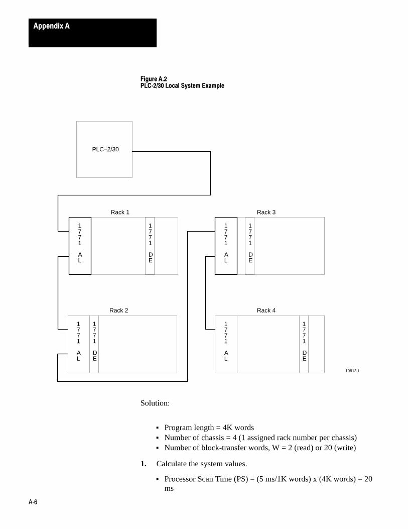
Example 2
A PLC-2/30 programmable controller is controlling four I/O racksin a local configuration. Assume one block-transfer module perchassis and one assigned rack number per chassis (Figure A.2).
Appendix A
A�6
Figure A.2PLC�2/30 Local System Example
PLC–2/30
1771
AL
1771
DE
Rack 1
1771
AL
1771
DE
Rack 3
1771
AL
1771
DE
Rack 4
1771
AL
1771
DE
Rack 2
10813-I
Solution:
Program length = 4K words Number of chassis = 4 (1 assigned rack number per chassis) Number of block-transfer words, W = 2 (read) or 20 (write)
1. Calculate the system values.
Processor Scan Time (PS) = (5 ms/1K words) x (4K words) = 20ms
Appendix A
A�7
Processor I/O Scan Time (PIO) = (0.5 ms/rack number) x (4 racknumbers) = 2 ms
Number of Words Transferred (W) = 2 (read) or 20 (write)
2. Calculate the block-transfer times (T) for the read and writeoperation.
T =0.08 ms/word x 2 words= .16 ms (read)
T =0.08 ms/word x 20 words= 1.6 ms (write)
3. Calculate the worst case system time (ST) between 2 consecutiveblock-transfer-read operations.
The module toggles to a read operation in the scan following completionof the write operation and vice versa.
ST =PS + PIO + T(1) + T(2) + T(3) + T(4)(writes) PS + PIO + T(1) + T(2) + T(3) + T(4)(reads)
ST =2PS + 2PIO + 4T(read) + 4T(write)=2(20) + 2(2) + 4(.16) + 4(1.6)=40 + 4 + .64 + 6.4=51.04 ms
This is the worst case time between two consecutive block-transfer-readoperations in the 4-chassis local configuration described in example 2(one enabled encoder module in each chassis).
Mini�PLC�2/15 Controller
The Mini-PLC-2/15 scan is 15 ms for 1K program. Its I/O scan time is 5ms. Each block-transfer module is updated during a program scan.
You can calculate the worst case time between transfers in two steps.
The facts are:
Processor scan time (PS) = 15 ms/1K words Processor I/O scan time (PIO) = 5 ms Number of words transferred (W) = 2 (read) or 20 (write)
1. Calculate the block-transfer time (T) for the read and write operation.
T =0.08 ms/word x number of words transferred
Appendix A
A�8
The same equation is used for read and write transfer times.
2. Calculate the worst case system time (ST) between twoblock-transfer-read operations.
ST =PS + PIO + T(read) + PS + PIO = T(write)
Example 3
A Mini-PLC-2/15 programmable controller is communicating withone encoder module in its I/O chassis. The ladder diagramprogram contains 2K words.
Solution:
The facts are:
Program length = 2K words Processor scan time (PS) = (15 ms/1K words) x (2K words) = 30
ms Processor I/O scan time (PIO) = 5 ms Number of words transferred (W) = 2 (read), 20 (write)
3. Calculate the block-transfer time (T) for the read and write operation.
T =0.08 ms/word x 2 words (read)=0.16 ms (read)
T =0.08 ms/word x 20 words (write)= 1.6 ms/(write)
4. Calculate the worst case system item (ST) between two consecutiveblock-transfer-read operations.
ST =PS + PIO + T(read) + PS + PIO + T(write)=30 + 5 + .16 + 30 + 5 + 1.6=71.76 ms
This is the worst case time between two consecutive block-transfer-readoperations for the Mini-PLC-2/15 controller.
The execution time required to complete a block-transfer-read or -writeoperation with a PLC-3 family processor depends on the number of:
words of user program active I/O channels on the scanner
Block�transfer Timing for PLC�3Family Processors
Appendix A
A�9
I/O chassis entries in the rack list for the channel I/O channels on the scanner that contain bloc-transfer modules block-transfer modules on the channel (if the I/O chassis containing a
block-transfer module appears more than once in the I/O chassis racklist, count the module once each time the chassis appears in the racklist).)
The typical time required for the encoder module to complete ablock-transfer-read/-write (bidirectional) depends on the program scanand the scanner scan as follows:
Time [read/write] = program scan + 2(scanner scan)
Program Scan: The program scan is approximately 2.5 ms per 1K wordsor user program when using examine on/off and block instructions.
Scanner Scan: The time required for the scanner to complete a re- orwrite-block transfer depends on the number of other block-transfermodules on the same scanner channel that are enabled simultaneously.
Block-transfer times typically are similar regardless of the type ofblock-transfer module, the number of words transferred, or whether a reador write operation is requested.
A block-transfer I/O channel is a channel that contains one or moreblock-transfer modules located in any chassis connected to the channel.
An I/O chassis can appear more than once in a rack list of I/O chassis.Count the chassis and the block-transfer module(s) that it contains asoften as it is listed.
The procedure for calculating block-transfer timing for a PLC-3 processoris given here followed by an example calculation:
1. Determine the number of active I/O channels on the scanner and thenumber of I/O channels with block-transfer modules. Show thenumber of:
block-transfer modules in each I/O chassis block-transfer I/O channels I/O chassis entries in the rack list for each block-transfer I/O
channel active I/O channels per scanner
Appendix A
A�10
2. Determine the nominal block-transfer time.
3. Compute the approximate scanner time for each block-transferchannel.
4. Compute the encoder re-/write-block-transfer time.
Example Computation
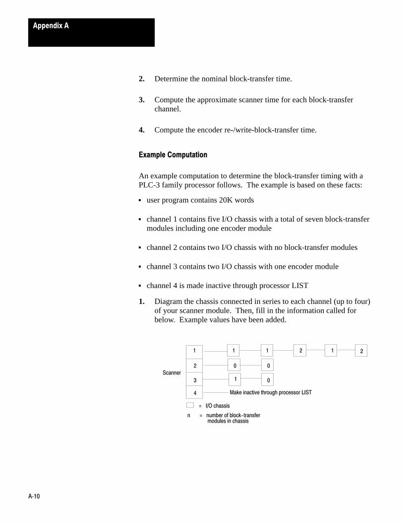
An example computation to determine the block-transfer timing with aPLC-3 family processor follows. The example is based on these facts:
user program contains 20K words
channel 1 contains five I/O chassis with a total of seven block-transfermodules including one encoder module
channel 2 contains two I/O chassis with no block-transfer modules
channel 3 contains two I/O chassis with one encoder module
channel 4 is made inactive through processor LIST
1. Diagram the chassis connected in series to each channel (up to four)of your scanner module. Then, fill in the information called forbelow. Example values have been added.
1
2
3
4
1 1 1
1
2
0
2
0
0
Make inactive through processor LIST
= I/O chassis
n = number of block-transfer modules in chassis
Scanner
Appendix A
A�11
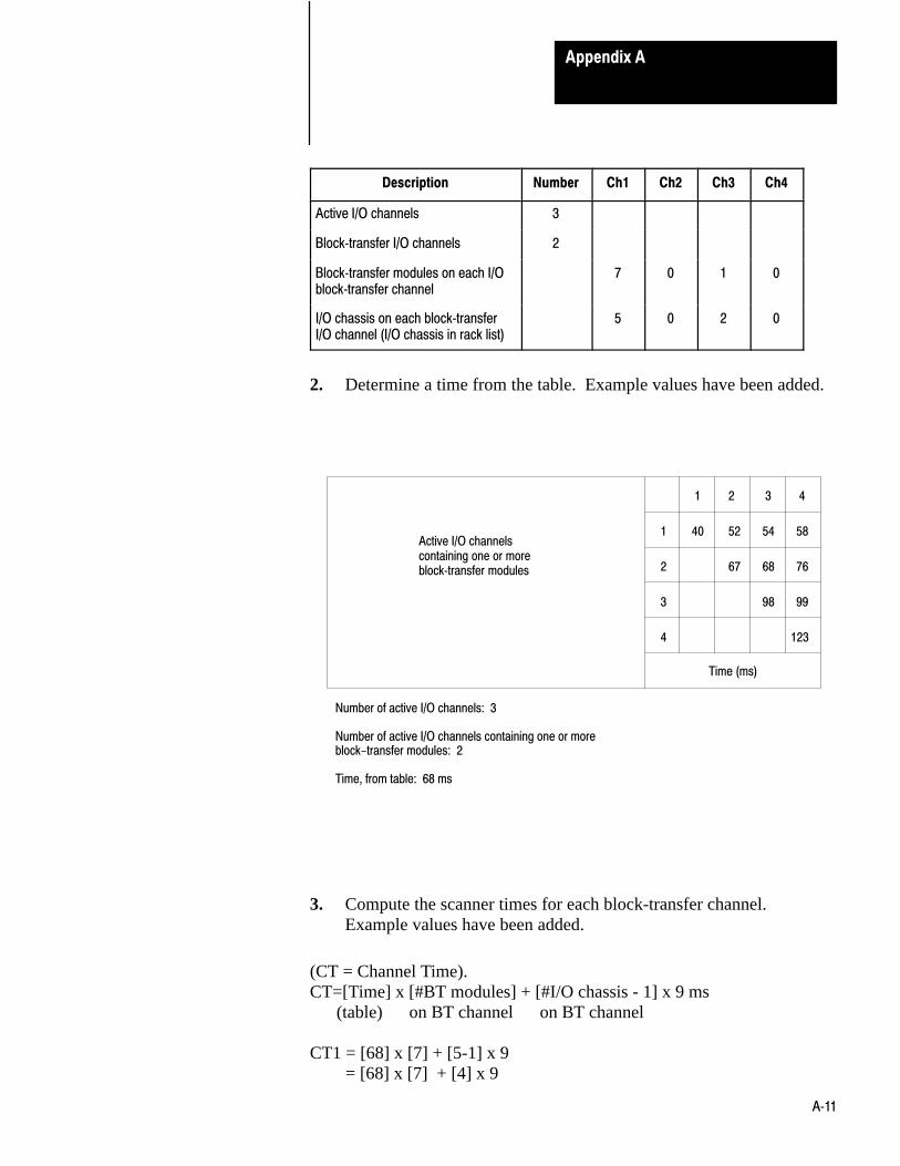
Description Number Ch1 Ch2 Ch3 Ch4
Active I/O channels 3
Block�transfer I/O channels 2
Block�transfer modules on each I/Oblock�transfer channel
7 0 1 0
I/O chassis on each block�transferI/O channel (I/O chassis in rack list)
5 0 2 0
2. Determine a time from the table. Example values have been added.
1 2 3 4
1 40 52 54 58
2 67 68 76
3 98 99
4 123
Time (ms)
Active I/O channels containing one or moreblock�transfer modules
Number of active I/O channels: 3
Number of active I/O channels containing one or moreblock-transfer modules: 2
Time, from table: 68 ms
3. Compute the scanner times for each block-transfer channel.Example values have been added.
(CT = Channel Time).CT=[Time] x [#BT modules] + [#I/O chassis - 1] x 9 ms (table) on BT channel on BT channel
CT1 = [68] x [7] + [5-1] x 9 = [68] x [7] + [4] x 9
Appendix A
A�12
= 476 + 36 = 512 ms CT2 = Not a block-transfer channel
CT3 = [68] x [1] + 1 x 9 = 68 + 9 = 77 ms
CT4 = Not an active channel
4. Compute the encoder read-/write-block-transfer time. Examplevalues have been added.
Program Scan:
Time (program)=2.5 ms/1K words x 20K words=2.5 x 20=50 ms
Scanner Scan:
Time (read or write) = 512 ms for channel 1 and 77 ms for channel 3(from Step 3).
Read/Write
Time =Program scan + 2 [Scanner scan](encoder =50 + 2 [512]module in =50 + 1024channel 1) =1074 ms
=1.1 seconds
Time =Program scan + 2 [Scanner scan](encoder =50 + 2[77]module in =204 mschannel 3)

Appendix
B
B�1
Application Considerations
The absolute encoder module can control outputs within a one-countresolution (turn an output on at position 065 and off at position 066) ifshaft speed does not exceed a certain limit. This speed limit depends onthe number of outputs and the number of counts on the encoder. It can befound from: S = K/Nwhere S = maximum shaft speed for one-count resolution; K = a constant;and N = number of counts on the encoder. The value of K depends onwhether you want to express shaft speed in revolutions per second (rps) orrevolutions per minute (rpm).
If you control: Then K = (for rps) OR K=(for rpm)
8 outputs 5000 300,000
6 outputs 6493 389,610
4 outputs 9009 540,540
2 outputs 14,084 845,070
For example, if you control eight outputs with a 0 to 359-count encoder,and the encoder shaft speed is given in revolutions per minute, theequation is:
300,000S = 360 = 833 rpm
The maximum encoder shaft speed at which you can control eight outputswithin a one-count resolution is 833 rpm.
Let’s consider two examples to show the importance of shaft speed,number of outputs to be controlled, and number of encoder counts inobtaining optimum module operation.
In both examples we use a 0 to 359-count encoder, all eight outputs areunder control, and the output is to turn on at position 000 and off atposition 001.
Application Considerations
Appendix B
B�2
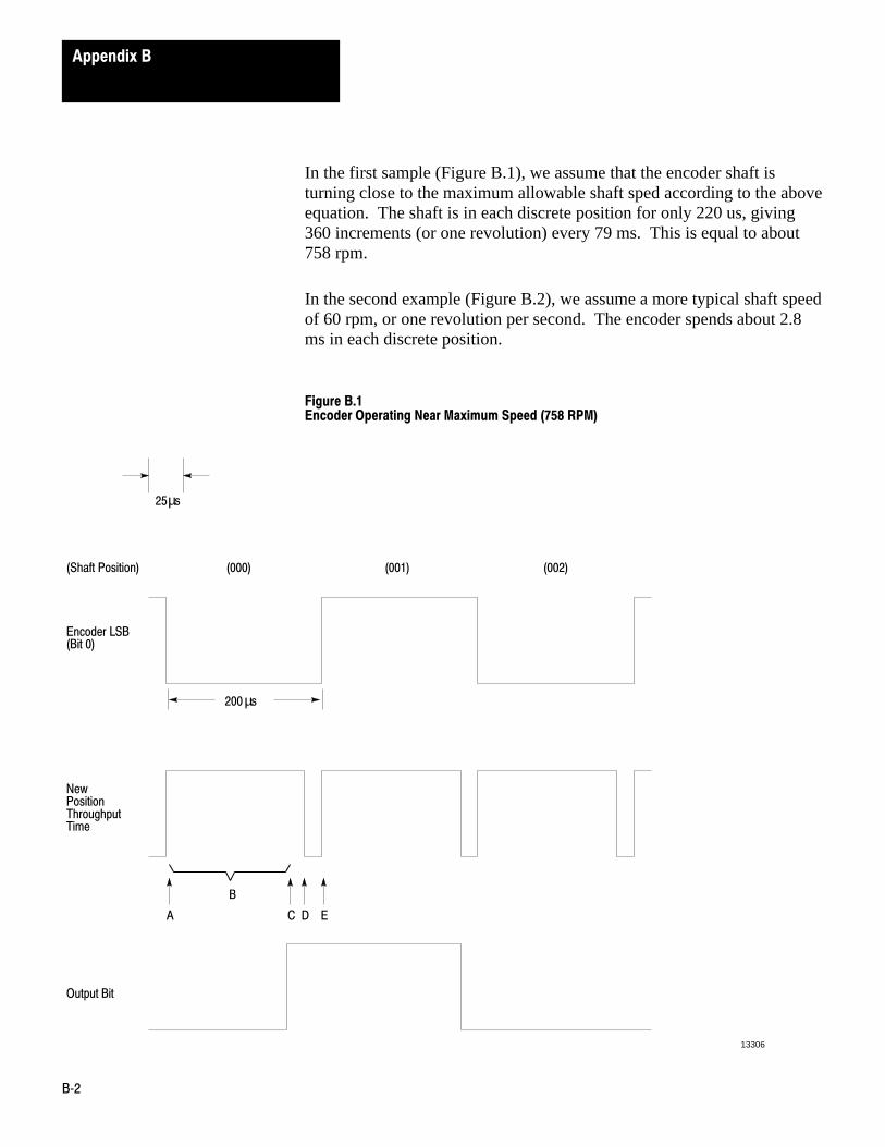
In the first sample (Figure B.1), we assume that the encoder shaft isturning close to the maximum allowable shaft sped according to the aboveequation. The shaft is in each discrete position for only 220 us, giving360 increments (or one revolution) every 79 ms. This is equal to about758 rpm.
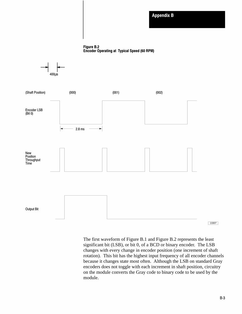
In the second example (Figure B.2), we assume a more typical shaft speedof 60 rpm, or one revolution per second. The encoder spends about 2.8ms in each discrete position.
Figure B.1Encoder Operating Near Maximum Speed (758 RPM)
25
(Shaft Position)
Encoder LSB(Bit 0)
New PositionThroughputTime
Output Bit
(000) (001) (002)
200
A
B
C D E
13306
µs
µs
Appendix B
B�3
Figure B.2Encoder Operating at Typical Speed (60 RPM)
400
(Shaft Position)
Encoder LSB(Bit 0)
New PositionThroughputTime
Output Bit
(000) (001) (002)
2.8 ms
13307
µs
The first waveform of Figure B.1 and Figure B.2 represents the leastsignificant bit (LSB), or bit 0, of a BCD or binary encoder. The LSBchanges with every change in encoder position (one increment of shaftrotation). This bit has the highest input frequency of all encoder channelsbecause it changes state most often. Although the LSB on standard Grayencoders does not toggle with each increment in shaft position, circuitryon the module converts the Gray code to binary code to be used by themodule.

Appendix B
B�4
The second waveform represents the new position throughput time of themodule. The third waveform represents an output programmed to turn onan actuator device (waveform high) when the encoder position is 000 andto turn it off (waveform low) when the encoder position is 001.
The new position throughput time of the module is based on the followingsequence of events:
a. The encoder shaft increases one position.
b. All 16 presets are compared to the encoder position.
c. The module updates the outputs.
d. The outputs are in the correct state for the given position, andthe scan period is complete.
e. The module scan begins with the next increase in the encodershaft position and the process then repeats.
Let’s look at the first example, where the encoder is operating nearmaximum speed and control is maintained over a one-count resolution.Comparing the input and output waveforms, the output bit comes on whenthe encoder position is almost 001 and turns off when the position isalmost 002. This is due to the time needed for the software comparison.
The second example shows waveforms for a speed of one revolution persecond. Control is easily maintained over a one-count resolution, and theoutput appears to follow the input more closely.
In both examples, the module throughput time is the same, dependingonly on the number of outputs to be controlled (see table below). Butwith increasingly lower input frequencies (slower shaft speed), the delayfrom change in input to output control is smaller compared to the inputperiod of an encoder increment.

Appendix B
B�5
WhenControlling:
New PositionThroughput Time is:
8 outputs 200 us
6 outputs 154 us
4 outputs 111 us
2 outputs 71 us
You must take into account the fixed throughput time, the number ofoutputs per module, and the number of increments between the presetvalues when determining the appropriate machine preset values for adesign shaft speed. Due to the effects shown in the first example, you maywant to adjust the preset values to account for the throughput time. Thisis important if the module is used near its maximum design speed.
If the maximum encoder shaft speed, determined from the aboveequations, is too slow for your application, you should consider thefollowing.
If you increase the input speed slightly, you can still maintain control to aone-count resolution. However, the encoder position value and the outputstatus read by the PC may not correspond. If, for example, you request anoutput to turn on at position 100, for one PC scan the PC might see aposition value of 099 while the output-on bit is set. The comparisons willbe performed correctly, but the status of the outputs read by the PC maynot correspond to the encoder position value.
This may not matter in your application if you do not use the read-data inyour PC application program. However, if this is not acceptable, you maybe able to trade resolution for speed. Remember that the maximum shaftspeed depends on the number of encoder positions. A 0 to 4,095-countencoder has a lower maximum rpm rating than a 0 to 359-count encoder.Similarly, a 0 to 99-count encoder turns at an even higher rotational speedto control within a one-count resolution.
You can also trade accuracy for speed. Suppose your application cantolerate having an output come on anywhere between position 030 and035 and go off between 045 and 050. The encoder shaft may be turningfast enough to go through several positions during the module comparisonprocessing time:
The module reads position 028 during the first module scan and leavesthe output off.

Appendix B
B�6
During the next scan the module reads position 032 and turns the outputon.
In this case you could program presets of 030 and 045 with theunderstanding that the change of output could occur a few incrementsafter those positions.
Hardware RC filtering in the module input circuitry is designed toattenuate high frequency noise spikes that may pass through the opto-isolators. The maximum practical input frequency to the module inputterminals is limited to 50KHz.
Appendix
C
C�1
Block�transfer Ladder Diagram Examples
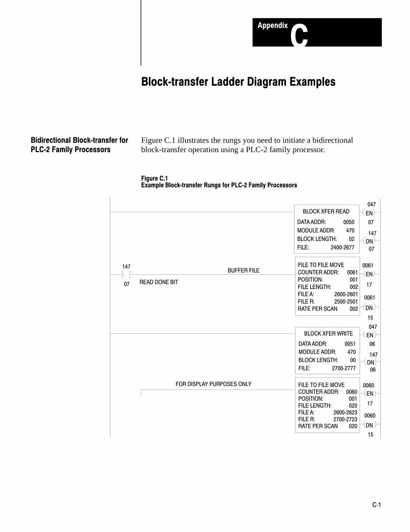
Figure C.1 illustrates the rungs you need to initiate a bidirectionalblock-transfer operation using a PLC-2 family processor.
Figure C.1Example Block�transfer Rungs for PLC�2 Family Processors
ENBLOCK XFER READ
DATA ADDR:
MODULE ADDR:
BLOCK LENGTH:
FILE:
0050
470
02
2400�2677DN
EN
FILE TO FILE MOVE
COUNTER ADDR:
POSITION:
FILE LENGTH:
FILE A:
0061
001
002
2600�2601
DNFILE R:
RATE PER SCAN
2500�2501
002
047
07
147
07
147
07
0061
17
0061
15
ENBLOCK XFER WRITE
DATA ADDR:
MODULE ADDR:
BLOCK LENGTH:
FILE:
0051
470
00
2700�2777DN
EN
FILE TO FILE MOVECOUNTER ADDR:POSITION:FILE LENGTH:FILE A:
0060001020
2600�2623
DNFILE R:RATE PER SCAN
2700�2723020
047
06
147
06
0060
17
0060
15
BUFFER FILE
READ DONE BIT
FOR DISPLAY PURPOSES ONLY
Bidirectional Block�transfer forPLC�2 Family Processors

Appendix C
C�2
Data Address: 0050/051
This is the first possible address in the timer/counter area of the data table.Use the first available timer/counter address for your first block-transfermodule data address.
Module Address: 470
The module is located in rack 4, I/O group 7, slot 0. (Two-slot modulesare addressed as being in slot 0.)
Block Length: 00
Use the default value for the maximum number of words to read (two)and write (20). Although both files appear to be 64 words long, only twowords are used for read operations and 20 words are used for writeoperations. The remaining words are available for storage.
File: 2600/2700
This is the address of the first word of the read/write file.
Use a file-to-file move to buffer your read data. Use addresses 2500 and2501 when making data comparisons.
Rung 4 is entered for display purposes only. You do not need this rung inyour program; it allows you to look at the read- and write-data filessimultaneously.
Figure C.2 shows example values entered in the read- and write-data files.These values were chosen for a 0 to 359-count BCD encoder.

Appendix C
C�3
Figure C.2Example Read�and Write�data File (PLC�2 Family Processors)
HEXADECIMAL DATA MONITORFILE TO FILE MOVE
POSITION: 001
COUNTER ADDR: 060FILE A: 2600 � 2623
FILE LENGTH: 020FILE R: 2700 � 2723
POSITION FILE A DATA FILE R DATA
001 0200 9E9E
002 0054 0000
003 0000 0044
004 0000 0045
005 0000 0089
006 0000 9E9E
007 0000 0090
008 0000 0134
009 0000 0135
010 0000 0179
011 0000 9E9E
012 0000 0180
013 0000 0224
014 0000 0225
015 0000 0269
016 0000 9E9E
017 0000 0270
018 0000 0314
019 0000 0315
020 0000 0359
READ�DATAFILE
WRITE�DATAFILE
In these file examples, word 1 in the read-data file indicates output 1 isenergized. Word 2 indicates that the current encoder position is 054.
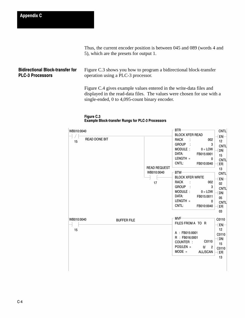
Appendix C
C�4
Thus, the current encoder position is between 045 and 089 (words 4 and5), which are the presets for output 1.
Figure C.3 shows you how to program a bidirectional block-transferoperation using a PLC-3 processor.
Figure C.4 gives example values entered in the write-data files anddisplayed in the read-data files. The values were chosen for use with asingle-ended, 0 to 4,095-count binary encoder.
Figure C.3Example Block�transfer Rungs for PLC�3 Processors
EN
BTR
BLOCK XFER READ
RACK :
GROUP :
MODULE :
002
3
0 = LOW
FB015:0001DN
0
FB010:0040 ER
DATA:
LENGTH =
CNTL:
WB010:0040
15
CNTL
12
CNTL
15
CNTL
13WB010:0040
17EN
BTW
BLOCK XFER WRITE
RACK :
GROUP :
MODULE :
002
3
0 = LOW
FB015:0011DN
0
FB010:0040 ER
DATA:
LENGTH =
CNTL:
CNTL
02
CNTL
05
CNTL
03
EN
MVF
FILES FROM A TO R
A : FB015:0001
R : FB016:0001 DN
0/ 2
ALL/SCAN ER
COUNTER :
POS/LEN =
MODE =
WB010:0040
15
C0110
12
C0110
15
C0110
13
C0110
BUFFER FILE
READ DONE BIT
READ REQUEST
Bidirectional Block�transfer forPLC�3 Processors

Appendix C
C�5
Use a file-to-file move to buffer the read data. Use B016:0001 (status)and B016:0002 (position) for all data comparisons.
Rack: 002
The module is located in rack 2.
Group: 3
The module is located in I/O group 3.
Module: 0 = low
The module is in the low slot of the I/O group. (Two-slot modules areaddressed as being in slot 0.)
Data: FB015:0001/FB015:0011
This is the address of the first word of the read/write file.
Length: 0
Use the default value for the maximum number of words to read (two)and write (20).
CNTL: FB010:0040/FB010:0040
This is the address of the block-transfer control file.
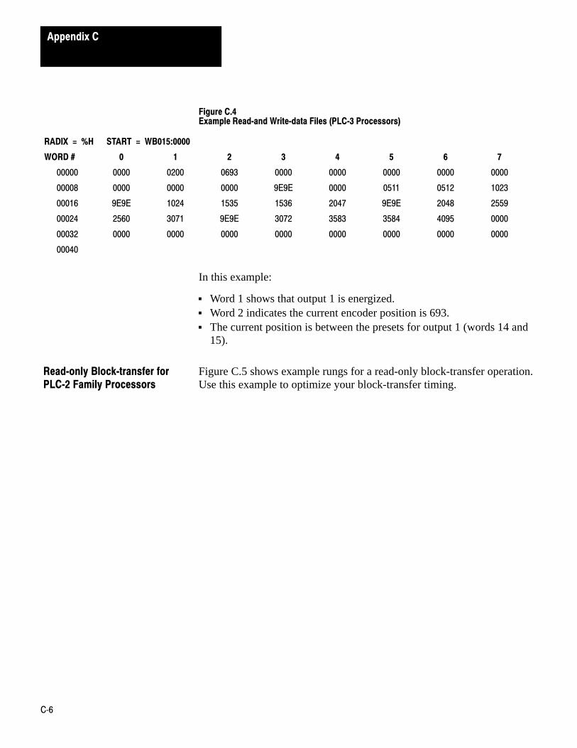
Appendix C
C�6
Figure C.4Example Read�and Write�data Files (PLC�3 Processors)
RADIX = %H START = WB015:0000
WORD # 0 1 2 3 4 5 6 7
00000 0000 0200 0693 0000 0000 0000 0000 0000
00008 0000 0000 0000 9E9E 0000 0511 0512 1023
00016 9E9E 1024 1535 1536 2047 9E9E 2048 2559
00024 2560 3071 9E9E 3072 3583 3584 4095 0000
00032 0000 0000 0000 0000 0000 0000 0000 0000
00040
In this example:
Word 1 shows that output 1 is energized. Word 2 indicates the current encoder position is 693. The current position is between the presets for output 1 (words 14 and
15).
Figure C.5 shows example rungs for a read-only block-transfer operation.Use this example to optimize your block-transfer timing.
Read�only Block�transfer forPLC�2 Family Processors
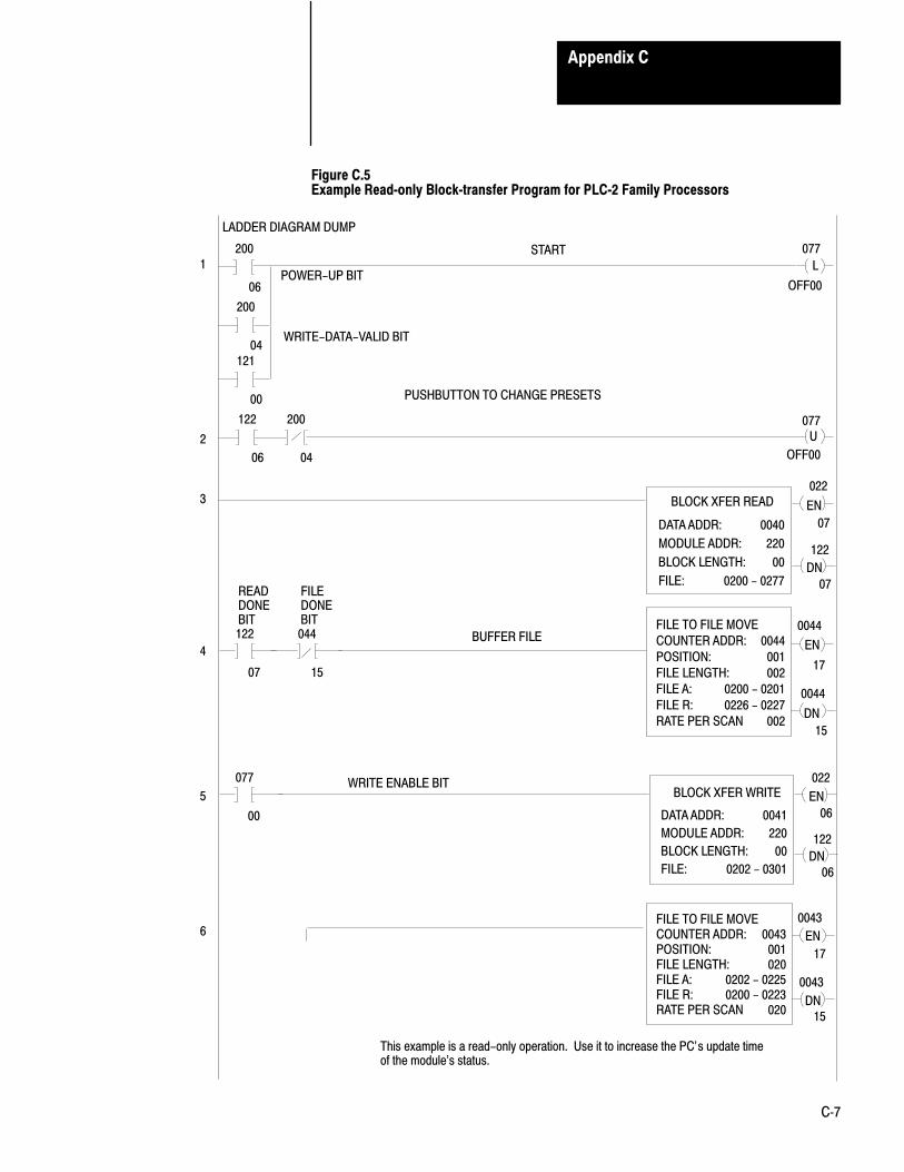
Appendix C
C�7
Figure C.5Example Read�only Block�transfer Program for PLC�2 Family Processors
ENBLOCK XFER READ
DATA ADDR:
MODULE ADDR:
BLOCK LENGTH:
FILE:
0040
220
00
0200 - 0277DN
EN
FILE TO FILE MOVE
COUNTER ADDR:
POSITION:
FILE LENGTH:
FILE A:
0044
001
002
0200 - 0201
DNFILE R:
RATE PER SCAN
0226 - 0227
002
022
07
122
07
122
07
0044
17
0044
15
ENBLOCK XFER WRITE
DATA ADDR:
MODULE ADDR:
BLOCK LENGTH:
FILE:
0041
220
00
0202 - 0301DN
EN
FILE TO FILE MOVECOUNTER ADDR:POSITION:FILE LENGTH:FILE A:
0043001020
0202 - 0225
DNFILE R:RATE PER SCAN
0200 - 0223020
022
06
122
06
0043
17
0043
15
200
06
L
200
04121
00
122
06
200
04
U
077
OFF00
077
OFF00
LADDER DIAGRAM DUMP
START
POWER-UP BIT
WRITE-DATA-VALID BIT
PUSHBUTTON TO CHANGE PRESETS
BUFFER FILE
READDONEBIT
044
15
FILEDONEBIT
077
00
WRITE ENABLE BIT
This example is a read-only operation. Use it to increase the PC's update timeof the module's status.
1
2
3
4
5
6

Appendix C
C�8
Rung 1 200/06 and 200/4 are returned in the read operation and latch077/00. When 077/00 is latched, the module toggles between aread operation and a write operation.
121/00 is optional and lets the processor initiate ablock�transfer�write operation.
Rung 2 This rung examines the write�done�bit (122/06) and the validBCD data bit (200/04) to unlatch 077/00 and begin theread�only operation.
Rung 3 This rung contains the block�transfer�read instruction.
Rung 4 Use a file�to�file move to buffer the read data. Use addresses0226 and 0227 when making any data comparisons.
Rung 5 A block�transfer�write is not done unless 077/00 is on.
Rung 6 This rung is for display purposes only.
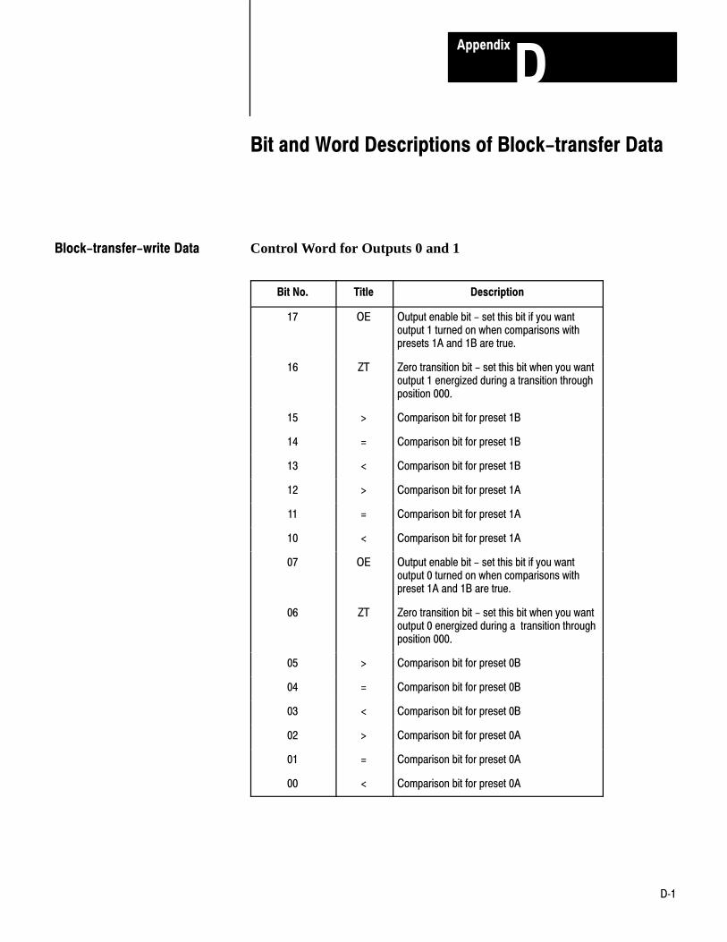
Appendix
D
D�1
Bit and Word Descriptions of Block-transfer Data
Control Word for Outputs 0 and 1
Bit No. Title Description
17 OE Output enable bit - set this bit if you wantoutput 1 turned on when comparisons withpresets 1A and 1B are true.
16 ZT Zero transition bit - set this bit when you wantoutput 1 energized during a transition throughposition 000.
15 > Comparison bit for preset 1B
14 = Comparison bit for preset 1B
13 < Comparison bit for preset 1B
12 > Comparison bit for preset 1A
11 = Comparison bit for preset 1A
10 < Comparison bit for preset 1A
07 OE Output enable bit - set this bit if you wantoutput 0 turned on when comparisons withpreset 1A and 1B are true.
06 ZT Zero transition bit - set this bit when you wantoutput 0 energized during a transition throughposition 000.
05 > Comparison bit for preset 0B
04 = Comparison bit for preset 0B
03 < Comparison bit for preset 0B
02 > Comparison bit for preset 0A
01 = Comparison bit for preset 0A
00 < Comparison bit for preset 0A
Block-transfer-write Data

Appendix D
D�2
Preset Words
WordNo. Description
2 Preset value A for output 0
3 Preset value B for output 0
4 Preset value A for output 1
5 Preset value B for output 1
7 Preset value A for output 2
8 Preset value B for output 2
9 Preset value A for output 3
10 Preset value B for output 3
12 Preset value A for output 4
13 Preset value B for output 4
14 Preset value A for output 5
15 Preset value B for output 5
17 Preset value A for output 6
18 Preset value B for output 6
19 Preset value A for output 7
20 Preset value B for output 7
Read-data Words
Word No. Bit No. Description
1 17 Status of output 7
16 Status of output 6
15 Status of output 5
14 Status of output 4
13 Status of output 3
12 Status of output 2
11 Status of output 1
10 Status of output 0
07 Loss-of-input-power bit - bit is set wheninput power is lost; it is reset when power isrestored and bit 6 is reset.
Block-transfer-read Data
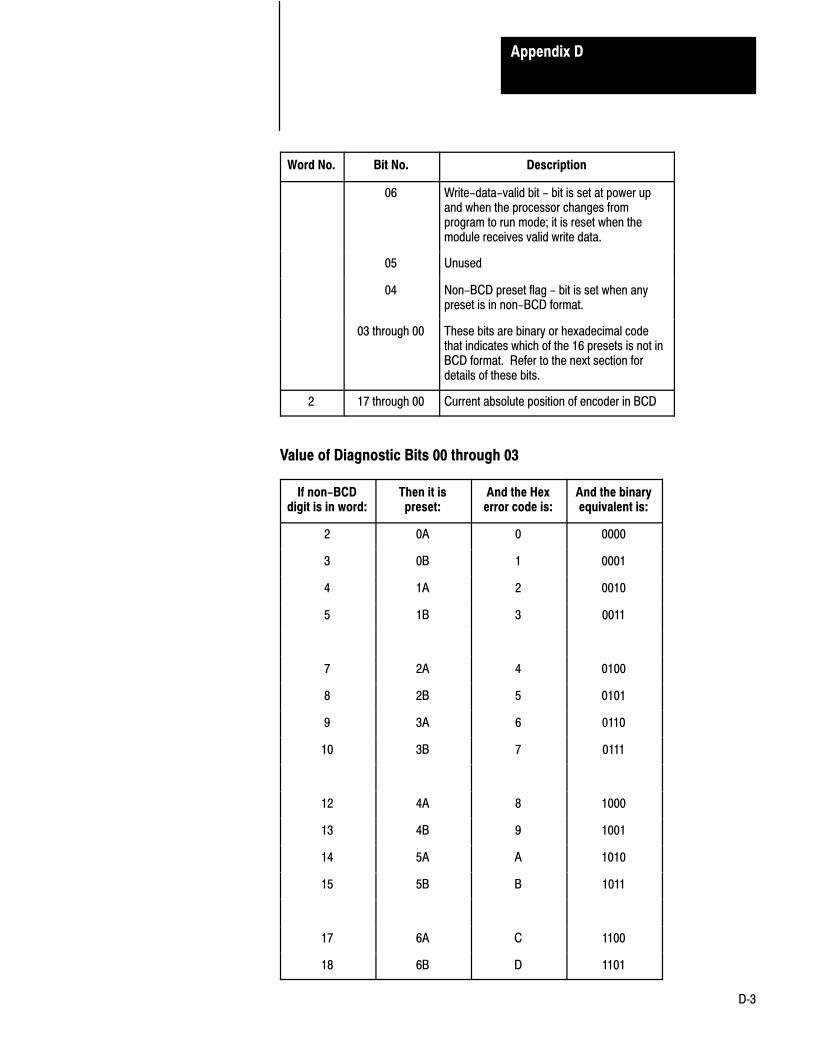
Appendix D
D�3
Word No. DescriptionBit No.
06 Write-data-valid bit - bit is set at power upand when the processor changes fromprogram to run mode; it is reset when themodule receives valid write data.
05 Unused
04 Non-BCD preset flag - bit is set when anypreset is in non-BCD format.
03 through 00 These bits are binary or hexadecimal codethat indicates which of the 16 presets is not inBCD format. Refer to the next section fordetails of these bits.
2 17 through 00 Current absolute position of encoder in BCD
Value of Diagnostic Bits 00 through 03
If non-BCDdigit is in word:
Then it ispreset:
And the Hexerror code is:
And the binaryequivalent is:
2 0A 0 0000
3 0B 1 0001
4 1A 2 0010
5 1B 3 0011
7 2A 4 0100
8 2B 5 0101
9 3A 6 0110
10 3B 7 0111
12 4A 8 1000
13 4B 9 1001
14 5A A 1010
15 5B B 1011
17 6A C 1100
18 6B D 1101

Appendix D
D�4
If non-BCDdigit is in word:
And the binaryequivalent is:
And the Hexerror code is:
Then it ispreset:
19 7A E 1110
20 7B F 1111

Appendix
E
E�1
Connection Diagrams for Allen�Bradley Encoders
Figures E.1 through Figure E.3 show you how to connect severalAllen-Bradley encoders to the absolute encoder module:
Figure E.1 shows you how to connect a Bulletin 845A encoder, 0 to359-count, 10-bit, BCD, single-ended output encoder.
Figure E.2 shows you how to connect a Bulletin 845A encoder, 0 to255-count, 8-bit, Standard Gray, single-ended output encoder.
Figure E.3 shows you the connections for a Bulletin 845C encoder, 0 to359-count, 10-bit, BCD, single-ended output, latching encoder.
Follow these guidelines:
Make the wht/orn wire (pin V) an open connection. The encoder counts up in a counterclockwise direction if you make the
wht/yel wire (pinQ) an open connection or if you connect it to +5V; ifyou connect it to ground, the encoder counts up in a clockwisedirection.
Signal common wht/blk (pin W) and ground blk (pin X) are internallyconnected on the encoder.
Jumper the unused most-significant-bit input terminals.
Connection Diagrams forAllen�Bradley Encoders
0 to 359�count, 10�bit, BCD,Single�ended Output
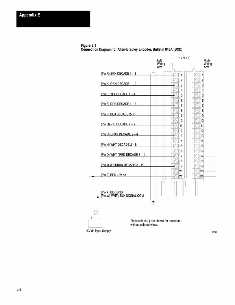
Appendix E
E�2
Figure E.1Connection Diagram for Allen�Bradley Encoder, Bulletin 845A (BCD)
1
2
3
4
5
6
7
8
9
10
11
12
13
14
15
16
17
18
19
20
21
1
2
3
4
5
6
7
8
9
10
11
12
13
14
15
16
17
18
19
20
21
LeftWiringArm
RightWiringArm
+5V dc Input Supply
+ -
13308
(Pin R) BRN DECADE 1 - 1
(Pin K) ORN DECADE 1 - 2
(Pin E) YEL DECADE 1 - 4
(Pin A) GRN DECADE 1 - 8
(Pin B) BLU DECADE 2-1
(Pin G) VIO DECADE 2 - 2
(Pin C) GRAY DECADE 2 - 4
(Pin H) WHT DECADE 2 - 8
(Pin D) WHT / RED DECADE 3 - 1
(Pin J) WHT/BRN DECADE 3 - 2
(Pin Z) RED +5V dc
(Pin X) BLK GND(Pin W) WHT / BLK SIGNAL COM
1771�DE
Pin locations ( ) are shown for encoders without colored wires.
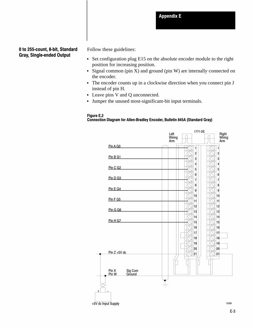
Appendix E
E�3
Follow these guidelines:
Set configuration plug E15 on the absolute encoder module to the rightposition for increasing position.
Signal common (pin X) and ground (pin W) are internally connected onthe encoder.
The encoder counts up in a clockwise direction when you connect pin Jinstead of pin H.
Leave pins V and Q unconnected. Jumper the unused most-significant-bit input terminals.
Figure E.2Connection Diagram for Allen�Bradley Encoder, Bulletin 845A (Standard Gray)
1
2
3
4
5
6
7
8
9
10
11
12
13
14
15
16
17
18
19
20
21
1
2
3
4
5
6
7
8
9
10
11
12
13
14
15
16
17
18
19
20
21
LeftWiringArm
RightWiringArm
+5V dc Input Supply
+ -
13309
Pin A G0
Pin B G1
Pin C G2
Pin D G3
Pin E G4
Pin F G5
Pin G G6
Pin H G7
Pin Z +5V dc
Pin XPin W
Sig ComGround
1771�DE
0 to 255�count, 8�bit, StandardGray, Single�ended Output

Appendix E
E�4
Follow these guidelines:
The encoder counts up in a counterclockwise direction if you make pinH an open connection or if you connect it to +5V; if you connect it toground, the encoder counts up in a clockwise direction.
Pins P, N, and V are internally connected on the encoder. Pins U, Z, T, and M are internally connected on the encode. Encoder output requires +5V DC; jumper pins P, N, and V to pin Y.
Leave pin L unconnected. Ground pin X for normal operation. Leave pins J, D, and Q unconnected. Jumper the unused most-significant-bit input terminals.
0 to 359�count, 10�bit, BCD,Single�ended Output, Latching
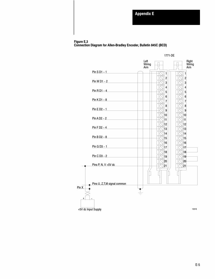
Appendix E
E�5
Figure E.3Connection Diagram for Allen�Bradley Encoder, Bulletin 845C (BCD)
1
2
3
4
5
6
7
8
9
10
11
12
13
14
15
16
17
18
19
20
21
1
2
3
4
5
6
7
8
9
10
11
12
13
14
15
16
17
18
19
20
21
LeftWiringArm
RightWiringArm
+5V dc Input Supply
+ -
13310
Pin S D1 - 1
Pin W D1 - 2
Pin R D1 - 4
Pin K D1 - 8
Pin E D2 - 1
Pin A D2 - 2
Pin F D2 - 4
Pin B D2 - 8
Pins P, N, V +5V dc
Pin X
Pins U, Z,T,M signal common
Pin G D3 - 1
Pin C D3 - 2
1771�DE
Appendix
F
F�1
Glossary
This glossary defines terms pertaining to Allen–Bradley AbsoluteEncoder Modules. For abroader glossary of programmable controllerwords, refer to our Programmable Controller Terms (publication no.PCGI–7.2).
ABSOLUTE ENCODER: An encoder with a unique digital output code for each increment of shaftrotation
BIDIRECTIONAL BLOCK TRANSFER:The performance of alternating read and write operations between anintelligent I/O module and the processor data table
DIFFERENTIAL OUTPUT ENCODER:An encoder using differential line driver output devices that have a bit xand bit x output signals
ENCODER DATA SETTLING TIME:The time required for encoder data to settle to reflect a new position
GRAY CODE:A binary numbering system modified so that only 1 bit changes as thecounting number increases.
MAXIMUM ENCODER SHAFT SPEED:The maximum speed at which the encoder shaft can turn to give aone–count resolution while controlling a particular number of outputs.
NEW POSITION THROUGHPUT TIME: The time between a certain state being applied to the input terminals and

Appendix F
F�2
the appropriate response occurring at the output terminals; it depends onthe number of outputs the module is controlling
NEW WRITE–DATA THROUGHPUT TIME:The time between the end of a block–transfer–write operation and themodule update of outputs
ONE–COUNT RESOLUTION:The ability of the module to perform within one increment of shaftrotation; for example, turn on an output at position 007 and off at position008
PRESET VALUE:The value against which the absolute position of the encoder is comparedto control an output
SINGLE–ENDED OUTPUT ENCODER:An encoder using single–ended (totem pole or open collector) outputdevices that have bit x and common output signals. Each bit may have acommon terminal, or all common terminals may be tied to the powersupply ground or common terminal in the encoder.

Symbols
**Empty**, 2�1, 2�2, 3�9, D�1
A
Application Considerations, B�1
B
Block-tranfer-write Data, 4�1
Block-transfer TimingPLC-2/15, A�7PLC-2/30 Local System, A�4PLC-2/30 Remote System, A�1PLC-3, A�9
Block-transfer-read Data, D�2
Block-transfer-read-Data, 4�4
C
Cabling, 3�8
Compatible Encoders, 2�2
Configuration Plugs, LocationSetting, 3�3Settings, 3�2
ConnectionsOutput Devices, 3�10Power Supplies, 3�5
Control Words, 4�3, D�1
D
Diagnostic Bits, D�3
E
Encoder, 3�9Format, 2�2, 3�3Input Signal Mode, 3�3
Example Applications, 2�1
F
Fuses, 2�3, 2�6
G
Glossary, F�1
I
Installation, 3�11
K
Keying, 2�7, 3�4
M
Module Functions, 2�1
module throughput time, B�4
O
one-count resolution, B�1
P
Power RequirementsInput, 2�6
Output, 3�5Output, 2�6, 3�7
Preset Words, 4�3, D�2
Programming Considerations, 4�7
Programming Example, 4�5
S
Specifications, 2�6
State of Output Upon Less of Input Power, 2�2
Status Indicator, 2�3
T
Terminal Identification, 2�5
Troubleshooting, 6�1
Index

Publication 1771-6.5.32 January 1986
Allen�Bradley, a Rockwell Automation Business, has been helping its customers improveproductivity and quality for more than 90 years. We design, manufacture and support a broadrange of automation products worldwide. They include logic processors, power and motioncontrol devices, operator interfaces, sensors and a variety of software. Rockwell is one of theworld's leading technology companies.
Worldwide representation.
Argentina • Australia • Austria • Bahrain • Belgium • Brazil • Bulgaria • Canada • Chile • China, PRC • Colombia • Costa Rica • Croatia • Cyprus • Czech Republic • Denmark •Ecuador • Egypt • El Salvador • Finland • France • Germany • Greece • Guatemala • Honduras • Hong Kong • Hungary • Iceland • India • Indonesia • Ireland • Israel • Italy •Jamaica • Japan • Jordan • Korea • Kuwait • Lebanon • Malaysia • Mexico • Netherlands • New Zealand • Norway • Pakistan • Peru • Philippines • Poland • Portugal • Puerto
Rico • Qatar • Romania • Russia-CIS • Saudi Arabia • Singapore • Slovakia • Slovenia • South Africa, Republic • Spain • Sweden • Switzerland • Taiwan • Thailand • Turkey •United Arab Emirates • United Kingdom • United States • Uruguay • Venezuela • Yugoslavia
Allen�Bradley Headquarters, 1201 South Second Street, Milwaukee, WI 53204 USA, Tel: (1) 414 382�2000 Fax: (1) 414 382�4444
Publication 1771-6.5.32 January 1986 PN 955096-76Copyright 1986 Allen�Bradley Company, Inc. Printed in USA