16-bit enhanced port expander with keypad and pwm ... sheets/st microelectronics...
TRANSCRIPT
February 2010 Doc ID 14318 Rev 6 1/62
62
STMPE160116-bit enhanced port expander with keypad and PWM controller
Xpander Logic™
Features■ 16 GPIOs
(8 operate at core supply VCC , 8 operate at IO supply VIO)
■ Operating voltage 1.8 −3.3 V
■ Hardware keypad controller (8*8 matrix with 4 optional dedicated keys max)
■ Keypad controller capable of detecting key-press in hibernation mode
■ 4 basic PWM controllers for LED brightness control
■ Interrupt output (open drain) pin
■ Optional 32 kHz clock input
■ 8-channel programmable level translator
■ Advanced power management system
■ Ultra-low standby-mode current
■ Package TFBGA25 (3 x 3 mm)
DescriptionThe STMPE1601 is a GPIO (general purpose input/output) port expander able to interface a main digital ASIC via the two-line bidirectional bus (I2C). A separate GPIO expander IC is often used in mobile multimedia platforms to solve the problems of the limited number of GPIOs typically available on the digital engine.
The STMPE1601 offers great flexibility, as each I/O can be configured as input, output or specific functions. The device is able to scan a keyboard, also provides PWM outputs for brightness control in backlight, and GPIO function. This device has been designed to include very low quiescent current, and a wake-up feature for each I/O, to optimize the power consumption of the IC.
Potential applications of the STMPE1601 include portable media players, game consoles, mobile and smart phones.
TFBGA25
Table 1. Device summary
Order code Package Packaging
STMPE1601TBR TFBGA25 Tape and reel
www.st.com
Contents STMPE1601
2/62 Doc ID 14318 Rev 6
Contents
1 Block diagram . . . . . . . . . . . . . . . . . . . . . . . . . . . . . . . . . . . . . . . . . . . . . . 4
2 Pin settings . . . . . . . . . . . . . . . . . . . . . . . . . . . . . . . . . . . . . . . . . . . . . . . . 5
2.1 Pin connection . . . . . . . . . . . . . . . . . . . . . . . . . . . . . . . . . . . . . . . . . . . . . . 5
2.2 Pin assignment and TFBGA ball location . . . . . . . . . . . . . . . . . . . . . . . . . . 5
2.3 Ball mapping to TFBGA (top through view) . . . . . . . . . . . . . . . . . . . . . . . . 6
2.4 GPIO pin functions . . . . . . . . . . . . . . . . . . . . . . . . . . . . . . . . . . . . . . . . . . . 7
3 Maximum rating . . . . . . . . . . . . . . . . . . . . . . . . . . . . . . . . . . . . . . . . . . . . . 8
3.1 Absolute maximum rating . . . . . . . . . . . . . . . . . . . . . . . . . . . . . . . . . . . . . . 8
3.2 Thermal data . . . . . . . . . . . . . . . . . . . . . . . . . . . . . . . . . . . . . . . . . . . . . . . 8
4 Electrical specification . . . . . . . . . . . . . . . . . . . . . . . . . . . . . . . . . . . . . . . 9
4.1 DC electrical characteristics . . . . . . . . . . . . . . . . . . . . . . . . . . . . . . . . . . . . 9
4.2 Input/Output DC electrical characteristics . . . . . . . . . . . . . . . . . . . . . . . . 10
5 Register map . . . . . . . . . . . . . . . . . . . . . . . . . . . . . . . . . . . . . . . . . . . . . . 11
6 I2C interface . . . . . . . . . . . . . . . . . . . . . . . . . . . . . . . . . . . . . . . . . . . . . . . 12
6.1 Minimizing current drain on I2C address lines . . . . . . . . . . . . . . . . . . . . . 13
6.2 Start condition . . . . . . . . . . . . . . . . . . . . . . . . . . . . . . . . . . . . . . . . . . . . . 14
6.3 Stop condition . . . . . . . . . . . . . . . . . . . . . . . . . . . . . . . . . . . . . . . . . . . . . 14
6.4 Acknowledge bit (ACK) . . . . . . . . . . . . . . . . . . . . . . . . . . . . . . . . . . . . . . . 14
6.5 Data input . . . . . . . . . . . . . . . . . . . . . . . . . . . . . . . . . . . . . . . . . . . . . . . . . 14
6.6 Slave device address . . . . . . . . . . . . . . . . . . . . . . . . . . . . . . . . . . . . . . . . 14
6.7 Memory addressing . . . . . . . . . . . . . . . . . . . . . . . . . . . . . . . . . . . . . . . . . 14
6.8 Operating modes . . . . . . . . . . . . . . . . . . . . . . . . . . . . . . . . . . . . . . . . . . . 15
6.9 General call address . . . . . . . . . . . . . . . . . . . . . . . . . . . . . . . . . . . . . . . . 16
7 System controller . . . . . . . . . . . . . . . . . . . . . . . . . . . . . . . . . . . . . . . . . . 17
7.1 States of operation . . . . . . . . . . . . . . . . . . . . . . . . . . . . . . . . . . . . . . . . . . 20
7.2 Autosleep . . . . . . . . . . . . . . . . . . . . . . . . . . . . . . . . . . . . . . . . . . . . . . . . . 21
7.3 Keypress detect in the hibernate mode . . . . . . . . . . . . . . . . . . . . . . . . . . 21
STMPE1601 Contents
Doc ID 14318 Rev 6 3/62
8 Clocking system . . . . . . . . . . . . . . . . . . . . . . . . . . . . . . . . . . . . . . . . . . . 22
8.1 Clock source . . . . . . . . . . . . . . . . . . . . . . . . . . . . . . . . . . . . . . . . . . . . . . . 22
8.2 Power mode programming sequence . . . . . . . . . . . . . . . . . . . . . . . . . . . . 23
9 Interrupt system . . . . . . . . . . . . . . . . . . . . . . . . . . . . . . . . . . . . . . . . . . . 24
9.1 Interrupt system register map . . . . . . . . . . . . . . . . . . . . . . . . . . . . . . . . . 24
9.1.1 Interrupt latency . . . . . . . . . . . . . . . . . . . . . . . . . . . . . . . . . . . . . . . . . . . 25
9.2 Programming sequence . . . . . . . . . . . . . . . . . . . . . . . . . . . . . . . . . . . . . . 30
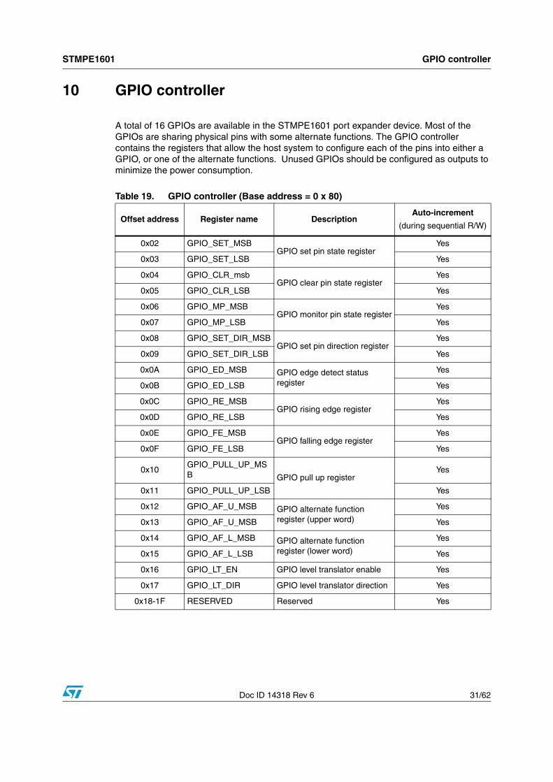
10 GPIO controller . . . . . . . . . . . . . . . . . . . . . . . . . . . . . . . . . . . . . . . . . . . . 31
10.1 GPIO control registers . . . . . . . . . . . . . . . . . . . . . . . . . . . . . . . . . . . . . . . 32
10.2 GPIO alternate function registers . . . . . . . . . . . . . . . . . . . . . . . . . . . . . . . 33
10.3 Hotkey feature . . . . . . . . . . . . . . . . . . . . . . . . . . . . . . . . . . . . . . . . . . . . . 34
10.3.1 Programming sequence for Hotkey . . . . . . . . . . . . . . . . . . . . . . . . . . . . 34
10.3.2 Minimum pulse width . . . . . . . . . . . . . . . . . . . . . . . . . . . . . . . . . . . . . . . 34
10.4 Level translator feature . . . . . . . . . . . . . . . . . . . . . . . . . . . . . . . . . . . . . . . 35
11 Basic PWM controller . . . . . . . . . . . . . . . . . . . . . . . . . . . . . . . . . . . . . . . 36
11.1 Interrupt on basic PWM controller . . . . . . . . . . . . . . . . . . . . . . . . . . . . . . 42
11.2 Trigger feature . . . . . . . . . . . . . . . . . . . . . . . . . . . . . . . . . . . . . . . . . . . . . 42
12 Keypad controller . . . . . . . . . . . . . . . . . . . . . . . . . . . . . . . . . . . . . . . . . . 43
12.1 Keypad configurations . . . . . . . . . . . . . . . . . . . . . . . . . . . . . . . . . . . . . . . 44
12.2 Keypad controller registers . . . . . . . . . . . . . . . . . . . . . . . . . . . . . . . . . . . . 46
13 Data registers . . . . . . . . . . . . . . . . . . . . . . . . . . . . . . . . . . . . . . . . . . . . . 50
14 Keypad combination key registers . . . . . . . . . . . . . . . . . . . . . . . . . . . . 53
15 Miscellaneous features . . . . . . . . . . . . . . . . . . . . . . . . . . . . . . . . . . . . . . 56
15.1 Reset . . . . . . . . . . . . . . . . . . . . . . . . . . . . . . . . . . . . . . . . . . . . . . . . . . . . 56
16 Package mechanical data . . . . . . . . . . . . . . . . . . . . . . . . . . . . . . . . . . . . 57
17 Revision history . . . . . . . . . . . . . . . . . . . . . . . . . . . . . . . . . . . . . . . . . . . 61

Block diagram STMPE1601
4/62 Doc ID 14318 Rev 6
1 Block diagram
Figure 1. STMPE1601 block diagram

STMPE1601 Pin settings
Doc ID 14318 Rev 6 5/62
2 Pin settings
2.1 Pin connection
Figure 2. Pin connection (top-through view)
2.2 Pin assignment and TFBGA ball location
GPIO_9
GPIO_8 GPIO_7 GPIO_5 GPIO_4
GPIO_11 GPIO_10 GPIO_6 CLK_IN INT
VIO GND GND GPIO_3 VCC
GPIO_12 GPIO_13 GPIO_1 GPIO_2
GPIO_14 GPIO_15
SCLK
SDATA RESET_N GPIO_0
1 2 3 4 5
A
B
C
D
E
AM00757V1
TFBGA25
Table 2. Pin assignment
Ball name Name Type Domain Description
E5 GPIO_0 I/O VCC GPIO 0/ KP_X0/ PWM_0
D4 GPIO_1 I/O VCC GPIO 1/ KP_X1/ PWM_1
D5 GPIO_2 I/O VCC GPIO 2/ KP_X2/ PWM_2
C4 GPIO_3 I/O VCC GPIO 3/ KP_X3/ PWM_3
A5 GPIO_4 I/O VCC GPIO 4/ KP_X4
A4 GPIO_5 I/O VCC GPIO 5/ KP_X5
B3 GPIO_6 I/O VCC GPIO 6/ KP_X6
A3 GPIO_7 I/O VCC GPIO 7/ KP_X7
A2 GPIO_8 I/O VIO GPIO 8/ KP_Y0
A1 GPIO_9 I/O VIO GPIO 9/ KP_Y1
B2 GPIO_10 I/O VIO GPIO 10/ KP_Y2

Pin settings STMPE1601
6/62 Doc ID 14318 Rev 6
2.3 Ball mapping to TFBGA (top through view)
Ball Name Name Type Domain Description
B1 GPIO_11 IO VIO GPIO 11/ KP_Y3
D1 GPIO_12 IO VIO GPIO 12/ KP_Y4
D2 GPIO_13 IO VIO GPIO 13/ KP_Y5/ ADDR0
E1 GPIO_14 IO VIO GPIO 14/ KP_Y6/ ADDR1
E2 GPIO_15 IO VIO GPIO 15/ KP_Y7/ ADDR2
B5 INT O VCC
Open drain interrupt output pin. INT pin to be externally pulled up to VCC(or > VCC, < 3.6 V), or pulled down to GND, depending on polarity of interrupt (must not be left floating).
E4 Reset_N I VCC
External reset input, active LOW. Reset_N pulse width must be ≥ 20 μs. This pin is internally pulled up to VCC.
E3 SDATA A VCC I2C DATA (tolerant to 3.6 V)
D3 SCLK A VCC I2C clock (tolerant to 3.6 V)
B4 CLK_IN A VCC
32 kHz input. To be pulled-up to VCC with 10 k resistor if clock is not used. This pin is internally pulled to VCC.
C5 VCC – –1.8 −3.3 V input for I2C module and digital core
C1 VIO – –1.8 −3.3 V input for GPIO. The VIO must be ≥ VCC.
C2 GND – – Ground
C3 GND – – Ground
Table 2. Pin assignment (continued)
Table 3. Pin mapping
1 2 3 4 5
A GPIO_9 GPIO_8 GPIO_7 GPIO_5 GPIO_4
B GPIO_11 GPIO_10 GPIO_6 CLK_IN INT
C VIO GND GND GPIO_3 VCC
D GPIO_12 GPIO_13 SCLK GPIO_1 GPIO_2
E GPIO_14 GPIO_15 SDATA RESET_N GPIO_0
STMPE1601 Pin settings
Doc ID 14318 Rev 6 7/62
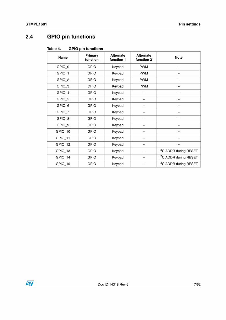
2.4 GPIO pin functions
Table 4. GPIO pin functions
NamePrimary function
Alternate function 1
Alternate function 2
Note
GPIO_0 GPIO Keypad PWM –
GPIO_1 GPIO Keypad PWM –
GPIO_2 GPIO Keypad PWM –
GPIO_3 GPIO Keypad PWM –
GPIO_4 GPIO Keypad – –
GPIO_5 GPIO Keypad – –
GPIO_6 GPIO Keypad – –
GPIO_7 GPIO Keypad – –
GPIO_8 GPIO Keypad – –
GPIO_9 GPIO Keypad – –
GPIO_10 GPIO Keypad – –
GPIO_11 GPIO Keypad – –
GPIO_12 GPIO Keypad – –
GPIO_13 GPIO Keypad – I2C ADDR during RESET
GPIO_14 GPIO Keypad – I2C ADDR during RESET
GPIO_15 GPIO Keypad – I2C ADDR during RESET
Maximum ratings STMPE1601
8/62 Doc ID 14318 Rev 6
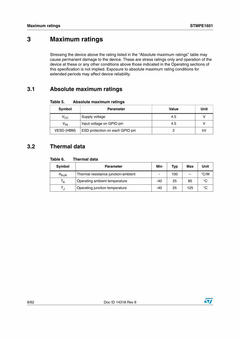
3 Maximum ratings
Stressing the device above the rating listed in the “Absolute maximum ratings” table may cause permanent damage to the device. These are stress ratings only and operation of the device at these or any other conditions above those indicated in the Operating sections of this specification is not implied. Exposure to absolute maximum rating conditions for extended periods may affect device reliability.
3.1 Absolute maximum ratings
3.2 Thermal data
Table 5. Absolute maximum ratings
Symbol Parameter Value Unit
VCC Supply voltage 4.5 V
VIN Input voltage on GPIO pin 4.5 V
VESD (HBM) ESD protection on each GPIO pin 2 kV
Table 6. Thermal data
Symbol Parameter Min Typ Max Unit
RthJA Thermal resistance junction-ambient - 100 – °C/W
TA Operating ambient temperature -40 25 85 °C
TJ Operating junction temperature -40 25 125 °C

STMPE1601 Electrical specification
Doc ID 14318 Rev 6 9/62
4 Electrical specification
4.1 DC electrical characteristics
Table 7. DC electrical characteristics
Symbol Parameter Test conditionsValue
UnitMin Typ Max
VCC 1.8 V supply voltage 1.65 − 3.6 V
VIO IO supply voltage 1.65 − 3.6 V
ICC Active currentVIO VCC = 1.8 V
T= 25 °C
– 1.2 1.6 mA
ISLEEP Sleep current – 18 25 µA
IHIBERNATE Hibernate current – 0.5 1.5 µA
ICC Active currentVIO VCC = 3.3 VT= 25 °C
– 3.0 3.8 mA
ISLEEP Sleep current – 50 60 µA
IHIBERNATE Hibernate current(1)
1. If only the basic GPIO function is required, the STMPE1601 can be designed to work mostly in hibernate mode. Active mode is used only when there are changes in the I/O status.
– 1.2 3 µA
ICC Active currentVIO VCC = 1.8 VT= 85 °C
– – 2 mA
ISLEEP Sleep current – – 32 µA
IHIBERNATE Hibernate current – – 2 µA
ICC Active currentVIO VCC = 3.3 VT= 85 °C
– – 4.8 mA
ISLEEP Sleep current – – 75 µA
IHIBERNATE Hibernate current(1) – – 5 µA
INTOpen drain output current
– 4 – mA

Electrical specification STMPE1601
10/62 Doc ID 14318 Rev 6
4.2 Input/Output DC electrical characteristicsThe 1.8 V I/O complies to the EIA/JEDEC standard JESD8-7.
Table 8. I/O DC electrical characteristic
Symbol ParameterValue
UnitMin Typ Max
Vil Low level input voltage VIO = 1.8 V – – 0.63 V
Vih High level input voltage VIO = 1.8 V 1.17 – – V
Vhyst Schmitt trigger hysteresis VIO = 1.8 V – 0.10 – V
Vil Low level input voltage VIO = 3.3 V – – 1.15 V
Vih High level input voltage VIO = 3.3 V 2.14 – – V
Vhyst Schmitt trigger hysteresis VIO = 3.3 V – 0.20 – V
Table 9. DC input specification (1.55 V < VCC < 1.95 V)
Symbol ParameterTest
conditions
ValueUnit
Min Typ Max
Vol Low level output voltageIol = 4 mA
VIO = 1.8 V– – 0.45 V
Voh High level output voltageIoh = 4 mA
VIO = 1.8 V1.35 – – V
Vol Low level output voltageIol = 4 mA
VIO = 3.3 V– – 0.83 V
Voh High level output voltageIoh = 4 mA
VIO = 3.3 V2.48 – – V
Table 10. DC output specification (1.55 V < VCC < 1.95 V)
Symbol Parameter Test conditionsValue
UnitMin Typ Max
Ipu Pull-up current VI = 0 V 15 35 65 μA
Rup(1)
1. Applicable to GPIO_0 to GPIO_7.
Equivalent pull-up resistance
VCC = 3.3 V 30 60 90 kΩ
VCC = 1.8 V 50 100 150 kΩ
Rup(2)
2. Applicable to GPIO_8 to GPIO_15.
Equivalent pull-up resistance
VIO = 3.3 V 30 60 90 kΩ
VIO = 1.8 V 50 100 150 kΩ
STMPE1601 Register map
Doc ID 14318 Rev 6 11/62
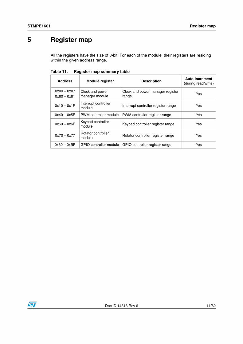
5 Register map
All the registers have the size of 8-bit. For each of the module, their registers are residing within the given address range.
Table 11. Register map summary table
Address Module register DescriptionAuto-increment
(during read/write)
0x00 – 0x07
0x80 – 0x81Clock and power manager module
Clock and power manager register range
Yes
0x10 – 0x1FInterrupt controller module
Interrupt controller register range Yes
0x40 – 0x5F PWM controller module PWM controller register range Yes
0x60 – 0x6FKeypad controller module
Keypad controller register range Yes
0x70 – 0x77Rotator controller module
Rotator controller register range Yes
0x80 – 0xBF GPIO controller module GPIO controller register range Yes
I2C interface STMPE1601
12/62 Doc ID 14318 Rev 6
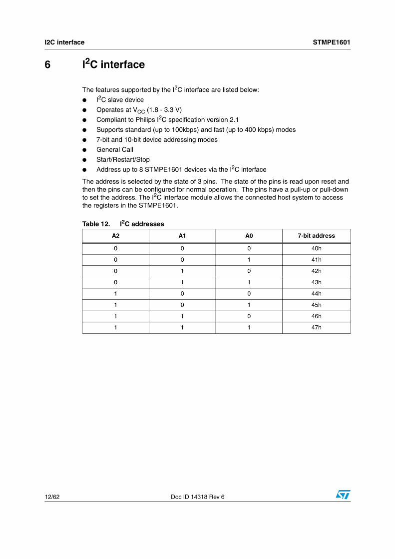
6 I2C interface
The features supported by the I2C interface are listed below:
● I2C slave device
● Operates at VCC (1.8 - 3.3 V)
● Compliant to Philips I2C specification version 2.1
● Supports standard (up to 100kbps) and fast (up to 400 kbps) modes
● 7-bit and 10-bit device addressing modes
● General Call
● Start/Restart/Stop
● Address up to 8 STMPE1601 devices via the I2C interface
The address is selected by the state of 3 pins. The state of the pins is read upon reset and then the pins can be configured for normal operation. The pins have a pull-up or pull-down to set the address. The I2C interface module allows the connected host system to access the registers in the STMPE1601.
Table 12. I2C addresses
A2 A1 A0 7-bit address
0 0 0 40h
0 0 1 41h
0 1 0 42h
0 1 1 43h
1 0 0 44h
1 0 1 45h
1 1 0 46h
1 1 1 47h
STMPE1601 I2C interface
Doc ID 14318 Rev 6 13/62
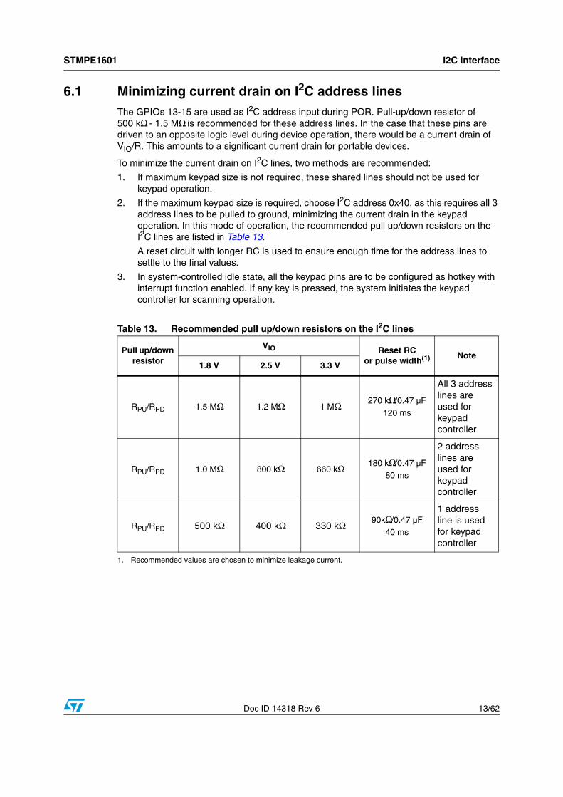
6.1 Minimizing current drain on I2C address linesThe GPIOs 13-15 are used as I2C address input during POR. Pull-up/down resistor of 500 kΩ - 1.5 MΩ is recommended for these address lines. In the case that these pins are driven to an opposite logic level during device operation, there would be a current drain of VIO/R. This amounts to a significant current drain for portable devices.
To minimize the current drain on I2C lines, two methods are recommended:
1. If maximum keypad size is not required, these shared lines should not be used for keypad operation.
2. If the maximum keypad size is required, choose I2C address 0x40, as this requires all 3 address lines to be pulled to ground, minimizing the current drain in the keypad operation. In this mode of operation, the recommended pull up/down resistors on the I2C lines are listed in Table 13.
A reset circuit with longer RC is used to ensure enough time for the address lines to settle to the final values.
3. In system-controlled idle state, all the keypad pins are to be configured as hotkey with interrupt function enabled. If any key is pressed, the system initiates the keypad controller for scanning operation.
Table 13. Recommended pull up/down resistors on the I2C lines
Pull up/down resistor
VIO Reset RCor pulse width(1)
1. Recommended values are chosen to minimize leakage current.
Note1.8 V 2.5 V 3.3 V
RPU/RPD 1.5 MΩ 1.2 MΩ 1 MΩ 270 kΩ/0.47 µF120 ms
All 3 address lines are used for keypad controller
RPU/RPD 1.0 MΩ 800 kΩ 660 kΩ 180 kΩ/0.47 µF80 ms
2 address lines are used for keypad controller
RPU/RPD 500 kΩ 400 kΩ 330 kΩ90kΩ/0.47 µF
40 ms
1 address line is used for keypad controller

I2C interface STMPE1601
14/62 Doc ID 14318 Rev 6
6.2 Start conditionA Start condition is identified by a falling edge of SDATA while SCLK is stable at high state. A Start condition must precede any data/command transfer. The device continuously monitors for a Start condition and does not respond to any transaction unless one is encountered.
6.3 Stop conditionA Stop condition is identified by a rising edge of SDATA while SCLK is stable at high state. A Stop condition terminates the communication between the slave device and bus master. A read command that is followed by NoAck can be followed by a Stop condition to force the slave device into idle mode. When the slave device is in idle mode, it is ready to receive the next I2C transaction. A Stop condition at the end of a write command stops the write operation to the registers.
6.4 Acknowledge bit (ACK)The acknowledge bit is used to indicate a successful byte transfer. The bus transmitter releases the SDATA after sending eight bits of data. During the ninth bit, the receiver pulls the SDATA low to acknowledge the receipt of the eight bits of data. The receiver may leave the SDATA in high state if it would to not acknowledge the receipt of the data.
6.5 Data inputThe device samples the data input on SDATA on the rising edge of the SCLK. The SDATA signal must be stable during the rising edge of SCLK and the SDATA signal must change only when SCLK is driven low.
6.6 Slave device addressThe slave device address is a 7 or 10-bit address, where the least significant 3-bit are programmable. These 3-bit values will be loaded in once upon reset and after that these 3 pins no longer be needed with the exception during General Call. Up to 8 STMPE1601 devices can be connected on a single I2C bus.
6.7 Memory addressingFor the bus master to communicate to the slave device, the bus master must initiate a Start condition and followed by the slave device address. Accompanying the slave device address, there is a Read/Write bit (R/W). The bit is set to 1 for Read and 0 for Write operation.
If a match occurs on the slave device address, the corresponding device gives an acknowledgement on the SDA during the 9th bit time. If there is no match, it deselects itself from the bus by not responding to the transaction.

STMPE1601 I2C interface
Doc ID 14318 Rev 6 15/62
6.8 Operating modes
Figure 3. I2C transaction
Table 14. Operating modes
Mode Bytes Programming sequence
Read ≥1
START, Device address, R/W = 0, Register address to be read
reSTART, Device address, R/W = 1, Data Read, STOP
If no STOP is issued, the Data Read can be continuously performed. If the register address falls within the range that allows address auto-increment, then register address auto-increments internally after every byte of data being read. For register address that falls within a non-incremental address range, the address will be kept static throughout the entire read operations. Refer to the Table 11: Register map summary table on page 11 for the address ranges that are auto and non-increment. An example of such a non-increment address is FIFO.
Write ≥1
START, Device address, R/W = 0, Register address to be written, Data Write, STOP.
If no STOP is issued, the Data Write can be continuously performed. If the register address falls within the range that allows address auto-increment, then register address auto-increments internally after every byte of data being written. For those register addresses that fall within a non-incremental address range, the address will be kept static throughout the all write operations. Refer to the memory map table for the address ranges that are auto and non-increment. An example of a non-increment address is Data Port for initializing the PWM commands.
Star
t
R/W
=0
AckDevice
AddressReg
Address Ack
Res
tart Device
Address Ack
R/W
=1 DataRead N
o Ac
k
StopOne byte
Read
Star
t
R/W
=0
AckDevice
AddressReg
Address Ack
Res
tart Device
Address Ack
R/W
=1 DataRead Ac
kMore than one byteRead Ac
k
No
Ack
StopData
Read + 1Data
Read + 2
Star
t
R/W
=0
AckDevice
AddressReg
Address Ack
Res
tart Data
to bewritten
Ack
StopOne byte
Write
More than one byteRead
Star
t
R/W
=0
AckDevice
AddressReg
Address Ack
Res
tart Data to
Write Ack
StopData to
Write + 2Ack
AckData to
Write + 1
Master
Slave
I2C interface STMPE1601
16/62 Doc ID 14318 Rev 6
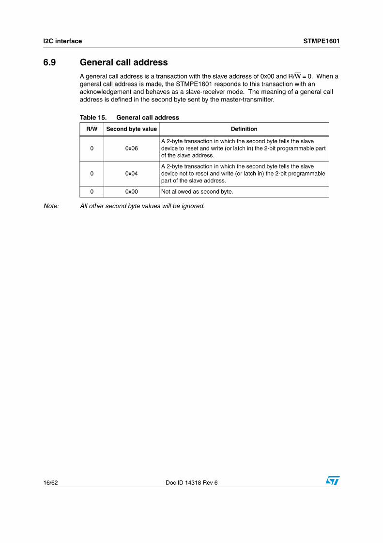
6.9 General call addressA general call address is a transaction with the slave address of 0x00 and R/W = 0. When a general call address is made, the STMPE1601 responds to this transaction with an acknowledgement and behaves as a slave-receiver mode. The meaning of a general call address is defined in the second byte sent by the master-transmitter.
Note: All other second byte values will be ignored.
Table 15. General call address
R/W Second byte value Definition
0 0x06A 2-byte transaction in which the second byte tells the slave device to reset and write (or latch in) the 2-bit programmable part of the slave address.
0 0x04A 2-byte transaction in which the second byte tells the slave device not to reset and write (or latch in) the 2-bit programmable part of the slave address.
0 0x00 Not allowed as second byte.
STMPE1601 System controller
Doc ID 14318 Rev 6 17/62
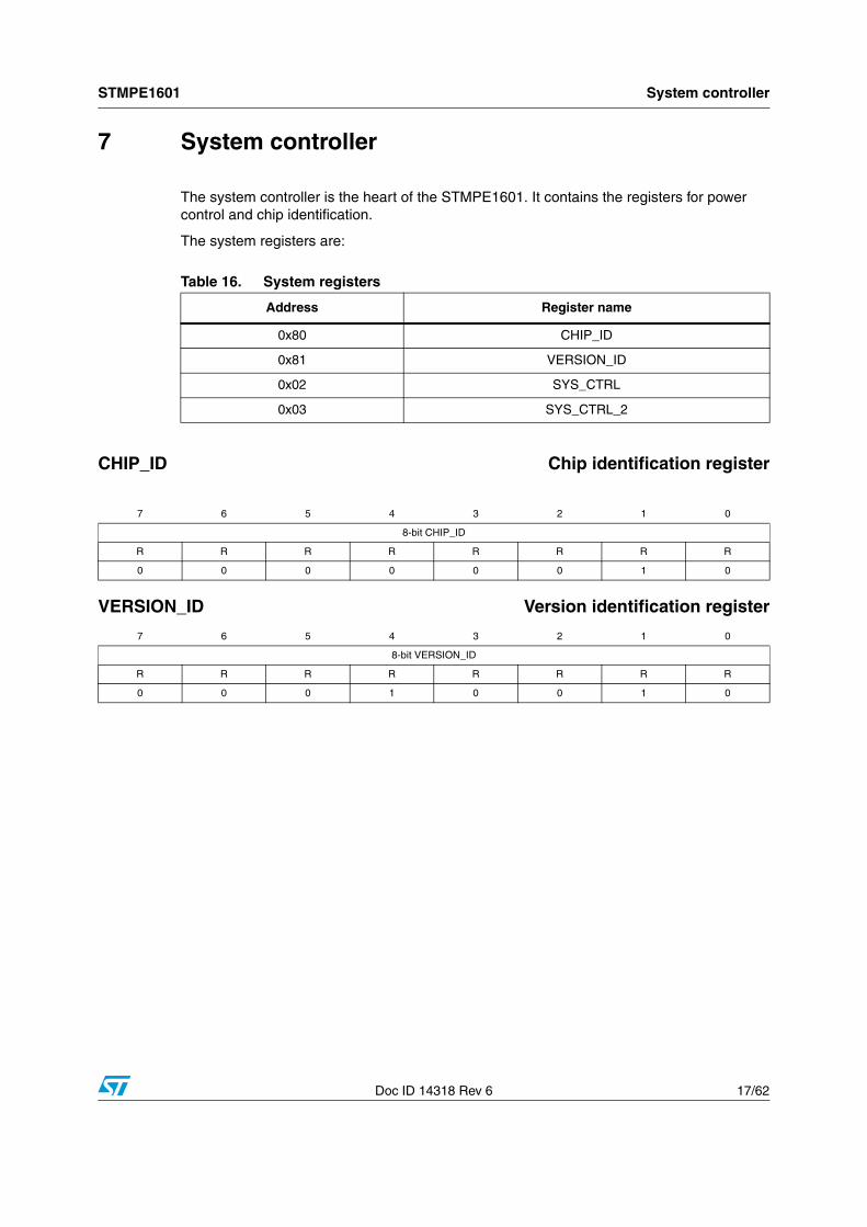
7 System controller
The system controller is the heart of the STMPE1601. It contains the registers for power control and chip identification.
The system registers are:
CHIP_ID Chip identification register
VERSION_ID Version identification register
Table 16. System registers
Address Register name
0x80 CHIP_ID
0x81 VERSION_ID
0x02 SYS_CTRL
0x03 SYS_CTRL_2
7 6 5 4 3 2 1 0
8-bit CHIP_ID
R R R R R R R R
0 0 0 0 0 0 1 0
7 6 5 4 3 2 1 0
8-bit VERSION_ID
R R R R R R R R
0 0 0 1 0 0 1 0
System controller STMPE1601
18/62 Doc ID 14318 Rev 6
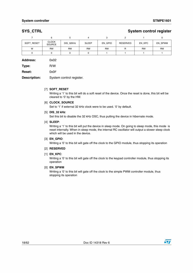
SYS_CTRL System control register
Address: 0x02
Type: R/W
Reset: 0x0F
Description: System control register.
7 6 5 4 3 2 1 0
SOFT_RESET CLOCK SOURCE DIS_32KHz SLEEP EN_GPIO RESERVED EN_KPC EN_SPWM
W RW RW RW RW R RW RW
0 0 0 0 1 1 1 1
[7] SOFT_RESETWriting a ‘1’ to this bit will do a soft reset of the device. Once the reset is done, this bit will be cleared to ‘0’ by the HW.
[6] CLOCK_SOURCESet to ‘1’ if external 32 kHz clock were to be used. ‘0’ by default.
[5] DIS_32 kHz:
Set this bit to disable the 32 kHz OSC, thus putting the device in hibernate mode.
[4] SLEEP:
Writing a ‘1’ to this bit will put the device in sleep mode. On going to sleep mode, this mode is reset internally. When in sleep mode, the internal RC oscillator will output a slower sleep clock which will be used in the device.
[3] EN_GPIO:
Writing a ‘0’ to this bit will gate off the clock to the GPIO module, thus stopping its operation
[2] RESERVED
[1] EN_KPC:
Writing a ‘0’ to this bit will gate off the clock to the keypad controller module, thus stopping its operation
[0] EN_SPWMWriting a ‘0’ to this bit will gate off the clock to the simple PWM controller module, thus stopping its operation
STMPE1601 System controller
Doc ID 14318 Rev 6 19/62
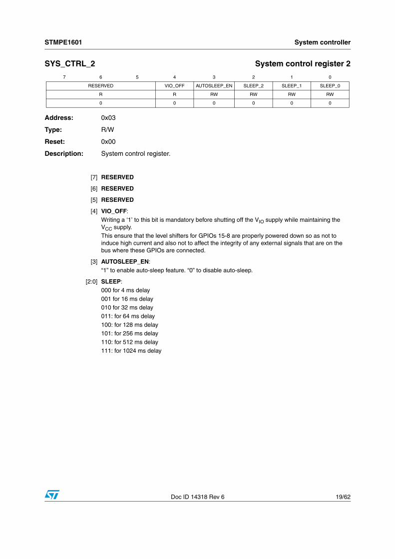
SYS_CTRL_2 System control register 2
Address: 0x03
Type: R/W
Reset: 0x00
Description: System control register.
7 6 5 4 3 2 1 0
RESERVED VIO_OFF AUTOSLEEP_EN SLEEP_2 SLEEP_1 SLEEP_0
R R RW RW RW RW
0 0 0 0 0 0
[7] RESERVED
[6] RESERVED
[5] RESERVED
[4] VIO_OFF:Writing a ‘1’ to this bit is mandatory before shutting off the VIO supply while maintaining the VCC supply. This ensure that the level shifters for GPIOs 15-8 are properly powered down so as not to induce high current and also not to affect the integrity of any external signals that are on the bus where these GPIOs are connected.
[3] AUTOSLEEP_EN:
“1” to enable auto-sleep feature. “0” to disable auto-sleep.
[2:0] SLEEP:
000 for 4 ms delay
001 for 16 ms delay010 for 32 ms delay
011: for 64 ms delay
100: for 128 ms delay101: for 256 ms delay
110: for 512 ms delay
111: for 1024 ms delay

System controller STMPE1601
20/62 Doc ID 14318 Rev 6
7.1 States of operation
Figure 4. Modes of operation
The device has three main modes of operation:
● Operational mode: This is the mode, whereby normal operation of the device takes place. In this mode, the RC clock is available and the main FSM unit routes this clock and the 32 kHz clock to all the device blocks that are enabled. In this mode, individual blocks that need not to be working can be turned off by the master by programming the bits 3 to 0 of the SYS_CTRL register.
● Sleep mode: In this low-power mode, the RC oscillator is powered down. All the blocks which need clocks derived from the 32 kHz clock will continue getting a 32 kHz clock. In this mode also, iindividual blocks can be turned off by the master by programming the bits 3 to 0 of the SYS_CTRL register. However, the master needs to program the SYS_CTRL register before coming into this mode, as in the sleep mode, the I2C interface is not active except to detect traffic for wakeup. Any activity on the I2C port (intended I2C transaction for the device) or Wakeup pin or Hotkey activity will cause the device to leave this mode and go into the Operational mode. When leaving this mode, the I2C will need to hold the SCLK till the RC clock is ready.
● Hibernate mode: This mode is entered when the system writes a ‘1’ to bit 5 of the SYS_CTRL register. In this mode, the device is completely inactive as there is absolutely no clock. Only a Reset or a wakeup on I2C will bring back the system to operational mode. A keypress detect will bring the system to Sleep mode, in which the debounce of the key will take place.
Note: The 32 kHz clock mentioned in this section can be (1) an externally fed 32 kHz clock, or (2) an internally generated (from RC OSC) clock. In case the internal clock is used, the clock has a range of 25 to 45 kHz.
OPERATIONAL
SLEEP
2
Set Disable_32K bit
Reset
HIBERNATE 32K: OFFRC: OFF
Set Sleep bit or autosleep
Valid Keypressdetect
I 2C transaction
Keypad, Interrupts&I C transaction
32K: ONRC: OFF
32K: ONRC: OFF
STMPE1601 System controller
Doc ID 14318 Rev 6 21/62
7.2 AutosleepThe host system may configure the STMPE1601 to go into sleep mode automatically whenever there is a period of inactivity following a complete I2C transaction with the STMPE1601. This inactivity means there is no intended I2C transaction for the device. For example, if there is an I2C transaction sent by the host to other slave devices, the STMPE1601 device will still be counting down for the auto-sleep. The STMPE1601 device resets the autosleep time-out counter only when it receives an I2C transaction meant for the device itself. This autosleep feature is controlled by the SYS_CTRL_2 (system control register 2).
All those events that trigger an interrupt (KPC, hot-key) would result in a transition from Sleep state to Operational state automatically. The wakeup can also be performed through the I2C transaction intended for the device.
7.3 Keypress detect in the hibernate modeWhen in Hibernate mode, a keypress detect causes the system to go into sleep mode. The sleep clock (32 kHz) is then used to debounce the key to detect a valid key. If the keypress is detected to be valid, the system stays in sleep mode. If the key is detected to be invalid, the system goes back into Hibernate mode.
Clocking system STMPE1601
22/62 Doc ID 14318 Rev 6
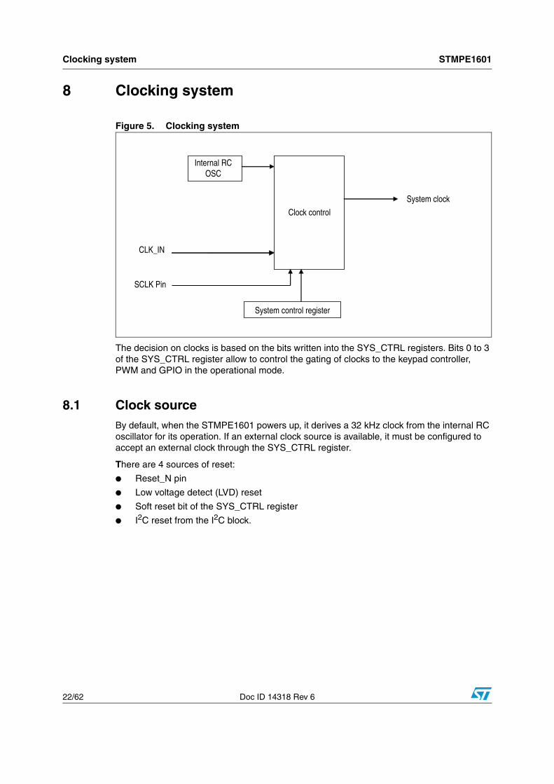
8 Clocking system
Figure 5. Clocking system
The decision on clocks is based on the bits written into the SYS_CTRL registers. Bits 0 to 3 of the SYS_CTRL register allow to control the gating of clocks to the keypad controller, PWM and GPIO in the operational mode.
8.1 Clock sourceBy default, when the STMPE1601 powers up, it derives a 32 kHz clock from the internal RC oscillator for its operation. If an external clock source is available, it must be configured to accept an external clock through the SYS_CTRL register.
There are 4 sources of reset:
● Reset_N pin
● Low voltage detect (LVD) reset
● Soft reset bit of the SYS_CTRL register
● I2C reset from the I2C block.
Internal RCOSC
Clock control
System control register
SCLK Pin
CLK_IN
System clock

STMPE1601 Clocking system
Doc ID 14318 Rev 6 23/62
8.2 Power mode programming sequenceTo put the device in sleep mode, the following needs to be done by the host:
– Write a '1' to bit 4 of the SYS_CTRL register.
To wake up the device, the host is required to:
– Assert a wakeup routine on the I2C bus by sending the Start bit, followed by the device address and the Write bit. Subsequently, proceed with sending the Base Register address and continue with a normal I2C transaction. The device wakes up upon receiving the correct device address and in Write direction. In other words, the procedure of waking up the device is performed by just sending an I2C transaction to the device. This procedure can be extended to wake up the device that is in hibernate mode.
To do a soft reset to the device, the host needs to do the following:
– Write a '1' to bit 7 of the SYS_CTRL register. This bit is automatically cleared upon reset.
To go into Hibernate mode, the following needs to be done by the host:
– Set the Disable_32K bit to '1'
To come out of the Hibernate mode, the following needs to be done by the host:
– Assert a system reset
– or put a wakeup on the I2C
Interrupt system STMPE1601
24/62 Doc ID 14318 Rev 6
9 Interrupt system
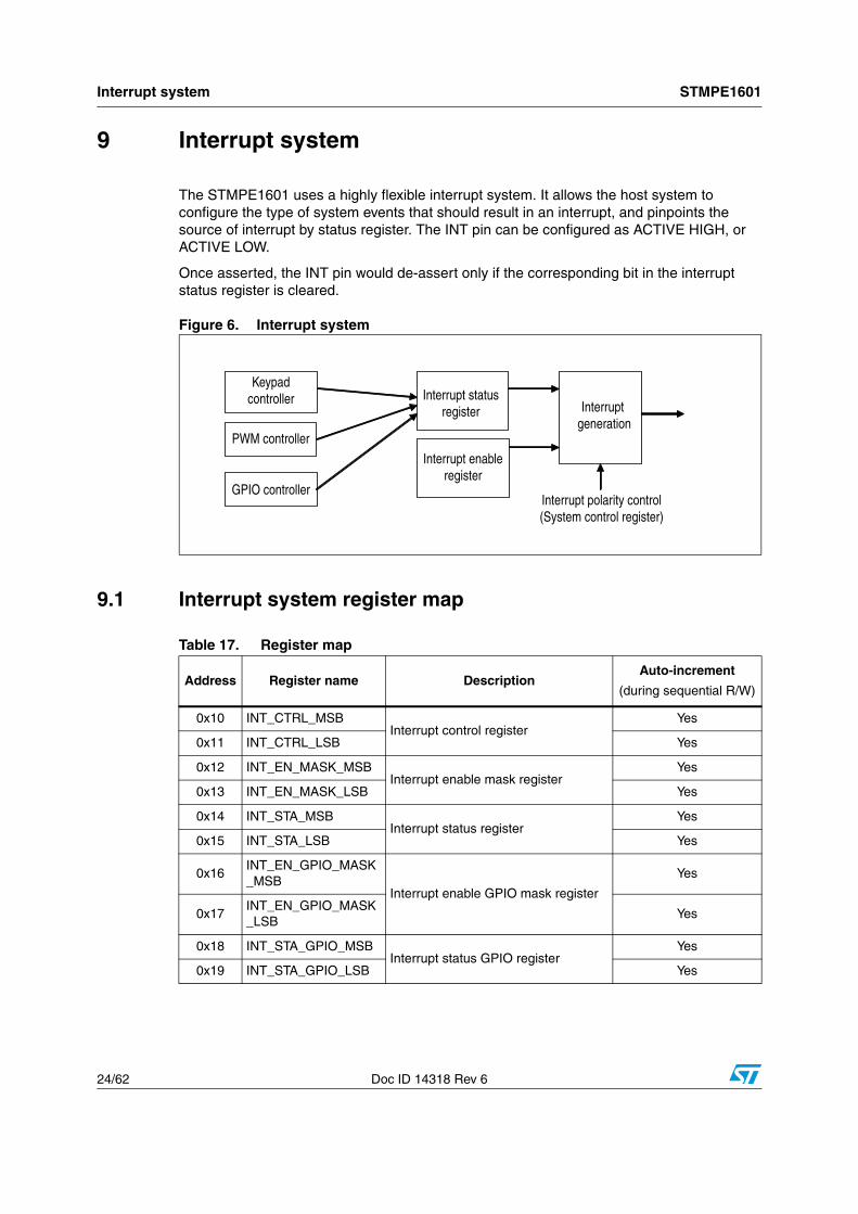
The STMPE1601 uses a highly flexible interrupt system. It allows the host system to configure the type of system events that should result in an interrupt, and pinpoints the source of interrupt by status register. The INT pin can be configured as ACTIVE HIGH, or ACTIVE LOW.
Once asserted, the INT pin would de-assert only if the corresponding bit in the interrupt status register is cleared.
Figure 6. Interrupt system
9.1 Interrupt system register map
Keypadcontroller
PWM controller
GPIO controller
Interrupt status register
Interrupt enable register
Interrupt generation
Interrupt polarity control(System control register)
Table 17. Register map
Address Register name DescriptionAuto-increment
(during sequential R/W)
0x10 INT_CTRL_MSBInterrupt control register
Yes
0x11 INT_CTRL_LSB Yes
0x12 INT_EN_MASK_MSBInterrupt enable mask register
Yes
0x13 INT_EN_MASK_LSB Yes
0x14 INT_STA_MSBInterrupt status register
Yes
0x15 INT_STA_LSB Yes
0x16INT_EN_GPIO_MASK_MSB
Interrupt enable GPIO mask register
Yes
0x17INT_EN_GPIO_MASK_LSB
Yes
0x18 INT_STA_GPIO_MSBInterrupt status GPIO register
Yes
0x19 INT_STA_GPIO_LSB Yes

STMPE1601 Interrupt system
Doc ID 14318 Rev 6 25/62
9.1.1 Interrupt latency
When the generation of interrupts by the GPIO as input is enabled, the latency (time taken from actual transition at GPIO to time of INT pin assertion) is shown in the following table:
INT_CTRL Interrupt control register
Address: 0x10, 0x11
Type: R, R/W
Reset: 0x00
Description: The interrupt control register is used to configure the interrupt controller. It has a global enable interrupt mask bit that controls the interruption to the host.
Table 18. Interrupt latency
State of operation Interrupt latency
Hibernation 10 µs max
Sleep 5 µs max
Active 2 µs max
15 14 13 12 11 10 9 8 7 6 5 4 3 2 1 0
INT_CTRL_msb INT_CTRL_lsb
Reserved IC2 IC1 IC0
R R R R R R R R R R R R R RW RW RW
0 0 0 0 0 0 0 0 0 0 0 0 0 0 0 0
[15:3] RESERVED
[2] IC2: Output Interrupt polarity
‘0’ = Active low/falling edge‘1’ = Active high/rising edge
[1] IC1: Output Interrupt Type‘0’ = Level interrupt
‘1’ = Edge interrupt
[0] IC0: Global Interrupt Mask bit
When this bit is written a ‘1’, it will allow interruption to the host. If it is written with a ‘0’, then, it disables all interruption to the host. Writing to this bit does not affect the INT_EN_MASK value.
Interrupt system STMPE1601
26/62 Doc ID 14318 Rev 6
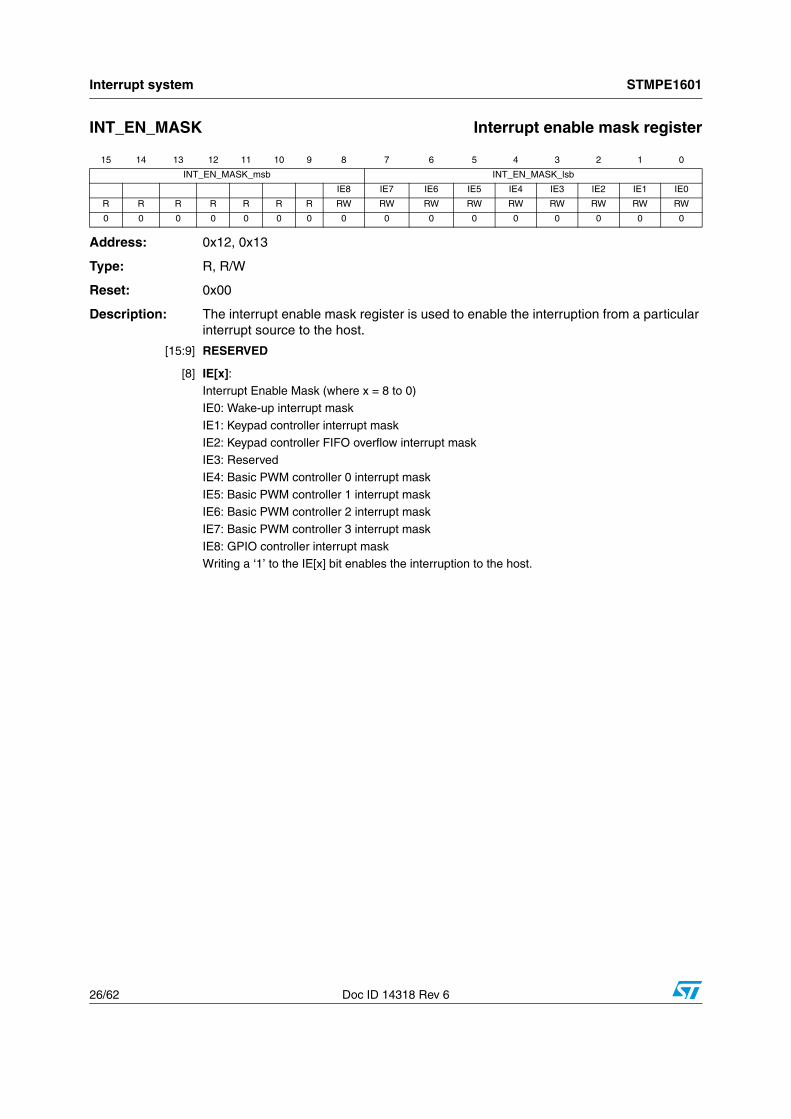
INT_EN_MASK Interrupt enable mask register
Address: 0x12, 0x13
Type: R, R/W
Reset: 0x00
Description: The interrupt enable mask register is used to enable the interruption from a particular interrupt source to the host.
15 14 13 12 11 10 9 8 7 6 5 4 3 2 1 0
INT_EN_MASK_msb INT_EN_MASK_lsb
IE8 IE7 IE6 IE5 IE4 IE3 IE2 IE1 IE0
R R R R R R R RW RW RW RW RW RW RW RW RW
0 0 0 0 0 0 0 0 0 0 0 0 0 0 0 0
[15:9] RESERVED
[8] IE[x]:Interrupt Enable Mask (where x = 8 to 0)
IE0: Wake-up interrupt mask
IE1: Keypad controller interrupt mask
IE2: Keypad controller FIFO overflow interrupt maskIE3: Reserved
IE4: Basic PWM controller 0 interrupt mask
IE5: Basic PWM controller 1 interrupt maskIE6: Basic PWM controller 2 interrupt mask
IE7: Basic PWM controller 3 interrupt mask
IE8: GPIO controller interrupt maskWriting a ‘1’ to the IE[x] bit enables the interruption to the host.

STMPE1601 Interrupt system
Doc ID 14318 Rev 6 27/62
INT_STA Interrupt status register
Address: 0x14, 0x15
Type: R, R/W
Reset: 0x00
Description: The interrupt status register monitors the status of the interruption from a particular interrupt source to the host. Regardless whether the INT_EN bits are enabled or not, the INT_STA bits are still updated.
15 14 13 12 11 10 9 8 7 6 5 4 3 2 1 0
ISR_msb ISR_lsb
IS8 IS7 IS6 IS5 IS4 IS3 IS2 IS1 IS0
R R R R R R R RW RW RW RW RW RW RW RW RW
0 0 0 0 0 0 0 0 0 0 0 0 0 0 0 0
[15:9] RESERVED
[8:0] IS[x]:Interrupt status (where x = 8 to 0)Read:
IS0: Wake-up Interrupt Status
IS1: Keypad controller interrupt statusIS2: Keypad controller FIFO overflow interrupt status
IS3: Reserved
IS4: Basic PWM controller 0 interrupt statusIS5: Basic PWM controller 1 interrupt status
IS6: Basic PWM controller 2 Interrupt status
IS7: Basic PWM controller 3 interrupt statusIS8: GPIO Controller Interrupt Status
Write: a write to a IS[x] bit with a value of ‘1’ will clear the interrupt and a write with a value of ‘0’ has no effect on the IS[x] bit.

Interrupt system STMPE1601
28/62 Doc ID 14318 Rev 6
INT_EN_GPIO_MASK Interrupt enable GPIO mask register
Address: 0x16, 0x17
Type: R/W
Reset: 0x00
Description: The interrupt enable GPIO mask register is used to enable the interruption from a particular GPIO interrupt source to the host. The IEG[15:0] bits are the interrupt enable mask bits correspond to the GPIO[15:0] pins
.
15 14 13 12 11 10 9 8 7 6 5 4 3 2 1 0
INT_EN_GPIO_MASK_msb INT_EN_GPIO_MASK _lsb
IEG15 IEG14 IEG13 IEG12 IEG11 IEG10 IEG9 IEG8 IEG7 IEG6 IEG5 IEG4 IEG3 IEG2 IEG1 IEG0
RW RW RW RW RW RW RW RW RW RW RW RW RW RW RW RW
0 0 0 0 0 0 0 0 0 0 0 0 0 0 0 0
[15:0] IEG[x]: interrupt enable GPIO mask (where x = 15 to 0)
Writing a ‘1’ to the IE[x] bit will enable the interruption to the host.

STMPE1601 Interrupt system
Doc ID 14318 Rev 6 29/62
INT_STA_GPIO Interrupt status GPIO register
Address: 0x18, 0x19
Type: R/W
Reset: 0x00
Description: The interrupt status GPIO register monitors the status of the interruption from a particular GPIO pin interrupt source to the host. Regardless whether the INT_EN_GPIO_MASK bits are enabled or not, the INT_STA_GPIO bits are still updated. The INT_STA_G[15:0] bits are the interrupt status bits correspond to the GPIO[15:0] pins.
15 14 13 12 11 10 9 8 7 6 5 4 3 2 1 0
INT_STA_GPIOR_msb INT_STA_GPIOR _lsb
ISG15 ISG14 ISG13 ISG12 ISG11 ISG10 ISG9 ISG8 ISG7 ISG6 ISG5 ISG4 ISG3 ISG2 ISG1 ISG0
RW RW RW RW RW RW RW RW RW RW RW RW RW RW RW RW
0 0 0 0 0 0 0 0 0 0 0 0 0 0 0 0
[15:0] ISG[x]Interrupt status GPIO (where x = 15 to 0)
Read:Interrupt status of the GPIO[x].Write:A write to a ISG[x] bit with a value of ‘1’ will clear the interrupt and a write with a value of ‘0’ has no effect on the ISG[x] bit.
Interrupt system STMPE1601
30/62 Doc ID 14318 Rev 6
9.2 Programming sequenceTo configure and initialize the interrupt controller to allow interruption to host, observe the following steps:
1. Set the INT_EN_MASK and INT_EN_GPIO_MASK registers to the desired values to enable the interrupt sources that are to be expected to receive from.
2. Configure the output interrupt type and polarity and enable the global interrupt mask by writing to the INT_CTRL.
3. Wait for interrupt.
4. Upon receiving an interrupt, the INT pin is asserted.
5. The host comes to read the INT_STA register through the I2C interface. A ‘1’ in the INT_STA bits indicates that the corresponding interrupt source is triggered.
6. If the IS8 bit in INT_STA register is set, the interrupt is coming from the GPIO controller. Then, a subsequent read is performed on the INT_STA_GPIO register to obtain the interrupt status of all 16 GPIOs to locate the GPIO that triggers the interrupt. This is a feature so-called ‘Hot Key’.
7. After obtaining the interrupt source that triggers the interrupt, the host performs the necessary processing and operations related to the interrupt source.
8. If the interrupt source is from the GPIO Controller, two write operations with value of ‘1’ are performed to the ISG[x] bit (INT_STA_GPIO) and the IS[8] (INT_STA) to clear the corresponding GPIO interrupt.
9. If the interrupt source is from other module, a write operation with value of ‘1’ is performed to the IS[x] (INT_STA) to clear the corresponding interrupt.
10. Once the interrupt is being cleared, the INT pin will also be de-asserted if the interrupt type is level interrupt. An edge interrupt will only assert a pulse width of 250ns.
11. When the interrupt is no longer required, the IC0 bit in INT_CTRL may be set to ‘0’ to disable the global interrupt mask bit.
STMPE1601 GPIO controller
Doc ID 14318 Rev 6 31/62
10 GPIO controller
A total of 16 GPIOs are available in the STMPE1601 port expander device. Most of the GPIOs are sharing physical pins with some alternate functions. The GPIO controller contains the registers that allow the host system to configure each of the pins into either a GPIO, or one of the alternate functions. Unused GPIOs should be configured as outputs to minimize the power consumption.
Table 19. GPIO controller (Base address = 0 x 80)
Offset address Register name DescriptionAuto-increment
(during sequential R/W)
0x02 GPIO_SET_MSBGPIO set pin state register
Yes
0x03 GPIO_SET_LSB Yes
0x04 GPIO_CLR_msbGPIO clear pin state register
Yes
0x05 GPIO_CLR_LSB Yes
0x06 GPIO_MP_MSBGPIO monitor pin state register
Yes
0x07 GPIO_MP_LSB Yes
0x08 GPIO_SET_DIR_MSBGPIO set pin direction register
Yes
0x09 GPIO_SET_DIR_LSB Yes
0x0A GPIO_ED_MSB GPIO edge detect status register
Yes
0x0B GPIO_ED_LSB Yes
0x0C GPIO_RE_MSBGPIO rising edge register
Yes
0x0D GPIO_RE_LSB Yes
0x0E GPIO_FE_MSBGPIO falling edge register
Yes
0x0F GPIO_FE_LSB Yes
0x10GPIO_PULL_UP_MSB GPIO pull up register
Yes
0x11 GPIO_PULL_UP_LSB Yes
0x12 GPIO_AF_U_MSB GPIO alternate function register (upper word)
Yes
0x13 GPIO_AF_U_MSB Yes
0x14 GPIO_AF_L_MSB GPIO alternate function register (lower word)
Yes
0x15 GPIO_AF_L_LSB Yes
0x16 GPIO_LT_EN GPIO level translator enable Yes
0x17 GPIO_LT_DIR GPIO level translator direction Yes
0x18-1F RESERVED Reserved Yes
GPIO controller STMPE1601
32/62 Doc ID 14318 Rev 6
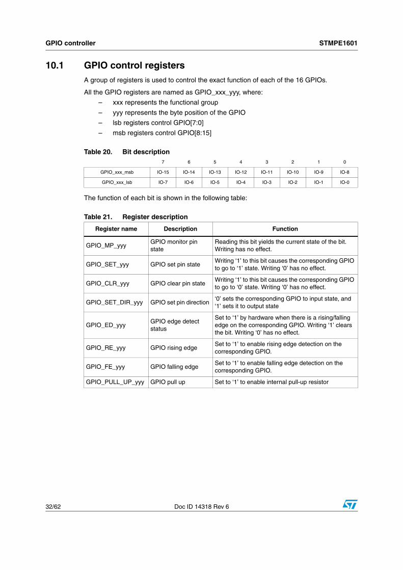
10.1 GPIO control registersA group of registers is used to control the exact function of each of the 16 GPIOs.
All the GPIO registers are named as GPIO_xxx_yyy, where:
– xxx represents the functional group
– yyy represents the byte position of the GPIO
– lsb registers control GPIO[7:0]
– msb registers control GPIO[8:15]
The function of each bit is shown in the following table:
Table 20. Bit description 7 6 5 4 3 2 1 0
GPIO_xxx_msb IO-15 IO-14 IO-13 IO-12 IO-11 IO-10 IO-9 IO-8
GPIO_xxx_lsb IO-7 IO-6 IO-5 IO-4 IO-3 IO-2 IO-1 IO-0
Table 21. Register description
Register name Description Function
GPIO_MP_yyyGPIO monitor pin state
Reading this bit yields the current state of the bit. Writing has no effect.
GPIO_SET_yyy GPIO set pin state Writing ‘1’ to this bit causes the corresponding GPIO to go to ‘1’ state. Writing ‘0’ has no effect.
GPIO_CLR_yyy GPIO clear pin state Writing ‘1’ to this bit causes the corresponding GPIO to go to ‘0’ state. Writing ‘0’ has no effect.
GPIO_SET_DIR_yyy GPIO set pin direction ‘0’ sets the corresponding GPIO to input state, and ‘1’ sets it to output state
GPIO_ED_yyyGPIO edge detect status
Set to ‘1’ by hardware when there is a rising/falling edge on the corresponding GPIO. Writing ‘1’ clears the bit. Writing ‘0’ has no effect.
GPIO_RE_yyy GPIO rising edgeSet to ‘1’ to enable rising edge detection on the corresponding GPIO.
GPIO_FE_yyy GPIO falling edgeSet to ‘1’ to enable falling edge detection on the corresponding GPIO.
GPIO_PULL_UP_yyy GPIO pull up Set to ‘1’ to enable internal pull-up resistor
STMPE1601 GPIO controller
Doc ID 14318 Rev 6 33/62
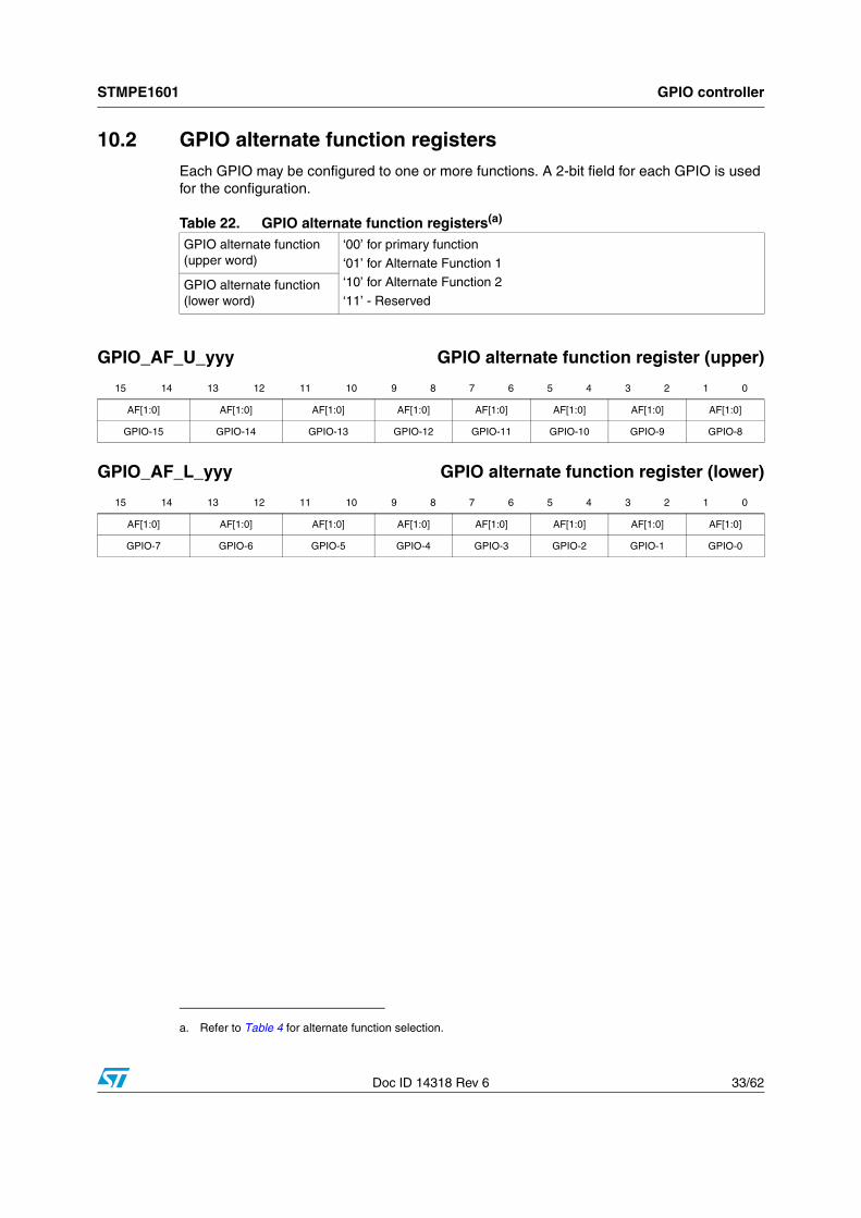
10.2 GPIO alternate function registersEach GPIO may be configured to one or more functions. A 2-bit field for each GPIO is used for the configuration.
Table 22. GPIO alternate function registers(a)
GPIO_AF_U_yyy GPIO alternate function register (upper)
GPIO_AF_L_yyy GPIO alternate function register (lower)
GPIO alternate function (upper word)
‘00’ for primary function
‘01’ for Alternate Function 1‘10’ for Alternate Function 2
‘11’ - ReservedGPIO alternate function (lower word)
a. Refer to Table 4 for alternate function selection.
15 14 13 12 11 10 9 8 7 6 5 4 3 2 1 0
AF[1:0] AF[1:0] AF[1:0] AF[1:0] AF[1:0] AF[1:0] AF[1:0] AF[1:0]
GPIO-15 GPIO-14 GPIO-13 GPIO-12 GPIO-11 GPIO-10 GPIO-9 GPIO-8
15 14 13 12 11 10 9 8 7 6 5 4 3 2 1 0
AF[1:0] AF[1:0] AF[1:0] AF[1:0] AF[1:0] AF[1:0] AF[1:0] AF[1:0]
GPIO-7 GPIO-6 GPIO-5 GPIO-4 GPIO-3 GPIO-2 GPIO-1 GPIO-0

GPIO controller STMPE1601
34/62 Doc ID 14318 Rev 6
10.3 Hotkey featureA GPIO is known as ‘Hotkey’ when it is configured to trigger an interruption to the host whenever the GPIO input is being asserted. This feature is applicable in Operational mode (4 MHz clock is present) as well as in Sleep mode (32 kHz clock is present).
10.3.1 Programming sequence for Hotkey
1. Configure the GPIO pin into GPIO mode by setting the corresponding bits in the GPIO alternate function register [GPIO_AF_x_yyy].
2. Configure the GPIO pin into input direction by setting the corresponding bit in the GPIO set pin direction registers [GPIO_SET_DIR_yyy].
3. Set the GPIO rising edge registers [GPIO_RE_yyy] and GPIO falling edge registers [GPIO_FE_yyy] to the desired values to enable the rising edge or falling edge detection.
4. Configure and enable the interrupt controller to allow the interruption to the host.
5. Now, the GPIO expander may be put into Sleep mode if it is desired.
6. Upon any hot-key being asserted, the device will wake up and issue an interrupt to the host.
Below are the conditions to be fulfilled in order to configure a Hot Key:
1. The pin is configured into GPIO mode and as input pin.
2. The global interrupt mask bit is enabled.
3. The corresponding GPIO interrupt mask bit is enabled.
10.3.2 Minimum pulse width
The minimum pulse width of the assertion of the Hotkey must be at least 62.5 us. Any pulse width less than the stated value may not be registered.
STMPE1601 GPIO controller
Doc ID 14318 Rev 6 35/62
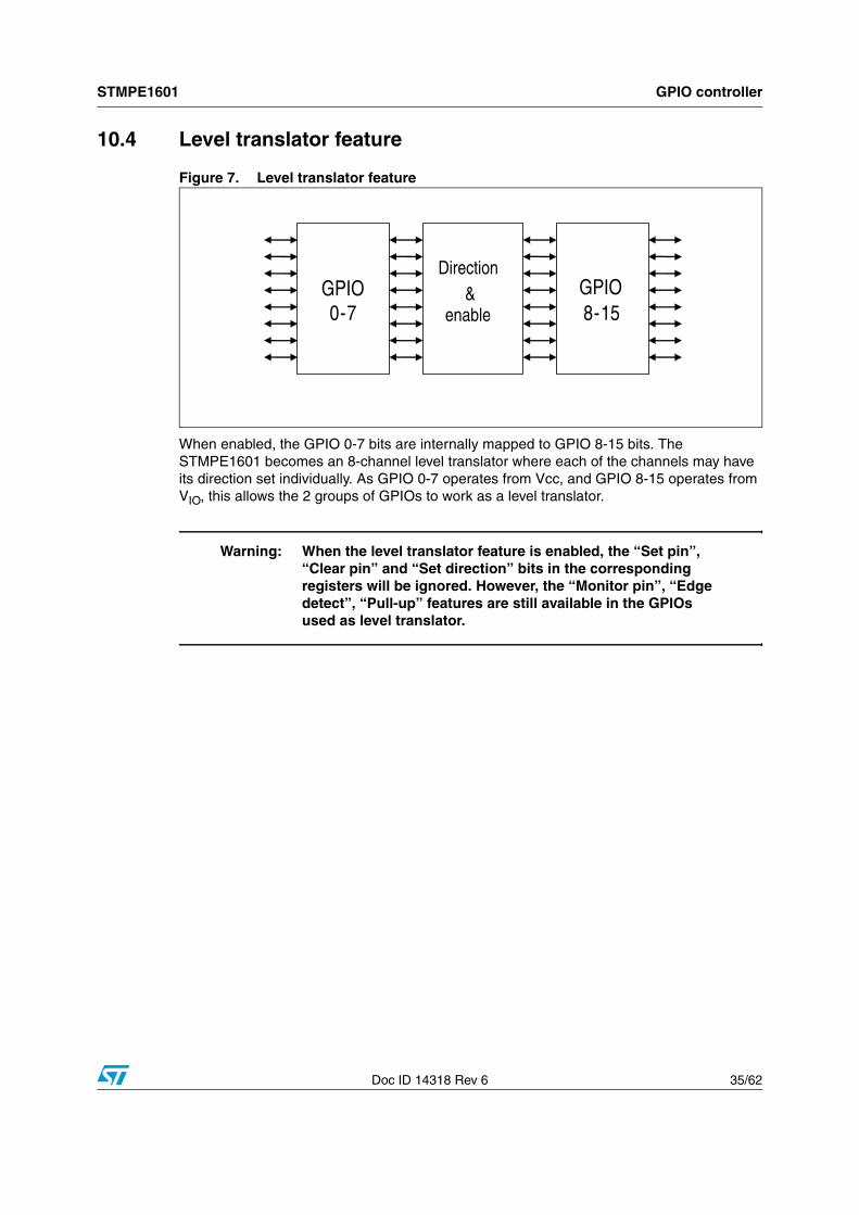
10.4 Level translator feature
Figure 7. Level translator feature
When enabled, the GPIO 0-7 bits are internally mapped to GPIO 8-15 bits. The STMPE1601 becomes an 8-channel level translator where each of the channels may have its direction set individually. As GPIO 0-7 operates from Vcc, and GPIO 8-15 operates from VIO, this allows the 2 groups of GPIOs to work as a level translator.
Warning: When the level translator feature is enabled, the “Set pin”, “Clear pin” and “Set direction” bits in the corresponding registers will be ignored. However, the “Monitor pin”, “Edge detect”, “Pull-up” features are still available in the GPIOs used as level translator.
GPIO 0-7
GPIO 8-15
Direction
&
enable
Basic PWM controller STMPE1601
36/62 Doc ID 14318 Rev 6
11 Basic PWM controller
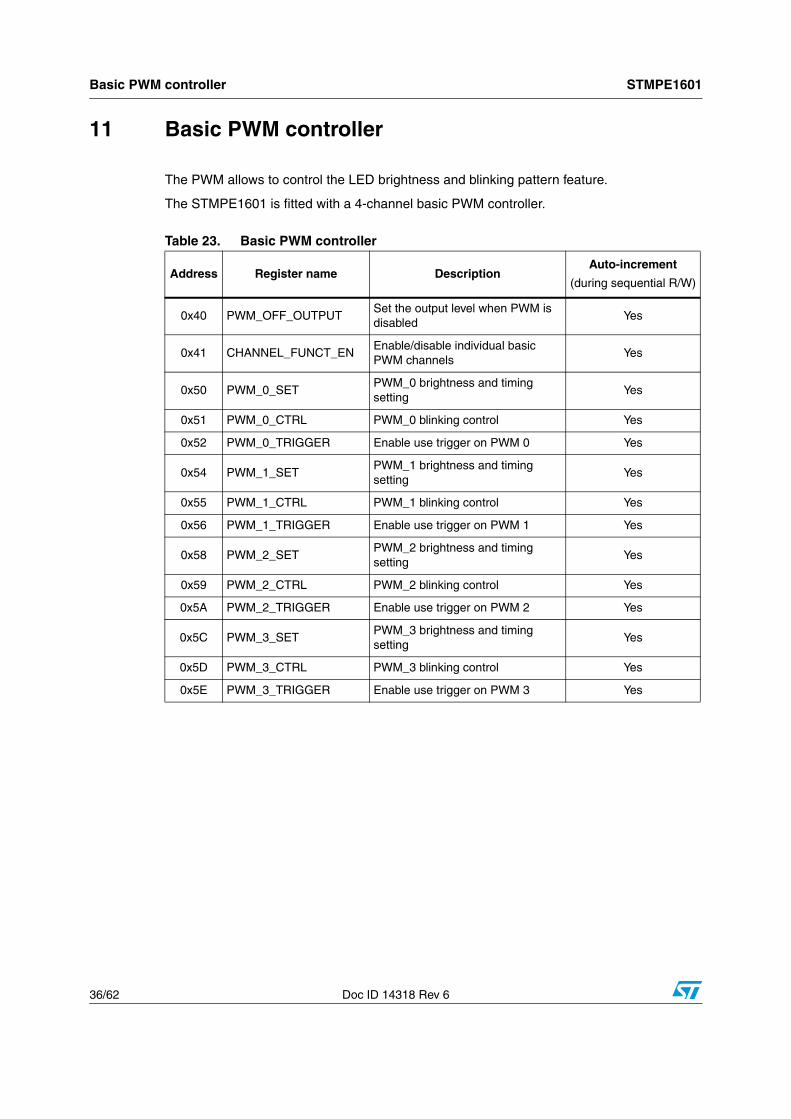
The PWM allows to control the LED brightness and blinking pattern feature.
The STMPE1601 is fitted with a 4-channel basic PWM controller.
Table 23. Basic PWM controller
Address Register name DescriptionAuto-increment
(during sequential R/W)
0x40 PWM_OFF_OUTPUTSet the output level when PWM is disabled
Yes
0x41 CHANNEL_FUNCT_EN Enable/disable individual basic PWM channels
Yes
0x50 PWM_0_SETPWM_0 brightness and timing setting
Yes
0x51 PWM_0_CTRL PWM_0 blinking control Yes
0x52 PWM_0_TRIGGER Enable use trigger on PWM 0 Yes
0x54 PWM_1_SETPWM_1 brightness and timing setting
Yes
0x55 PWM_1_CTRL PWM_1 blinking control Yes
0x56 PWM_1_TRIGGER Enable use trigger on PWM 1 Yes
0x58 PWM_2_SETPWM_2 brightness and timing setting
Yes
0x59 PWM_2_CTRL PWM_2 blinking control Yes
0x5A PWM_2_TRIGGER Enable use trigger on PWM 2 Yes
0x5C PWM_3_SETPWM_3 brightness and timing setting
Yes
0x5D PWM_3_CTRL PWM_3 blinking control Yes
0x5E PWM_3_TRIGGER Enable use trigger on PWM 3 Yes
STMPE1601 Basic PWM controller
Doc ID 14318 Rev 6 37/62
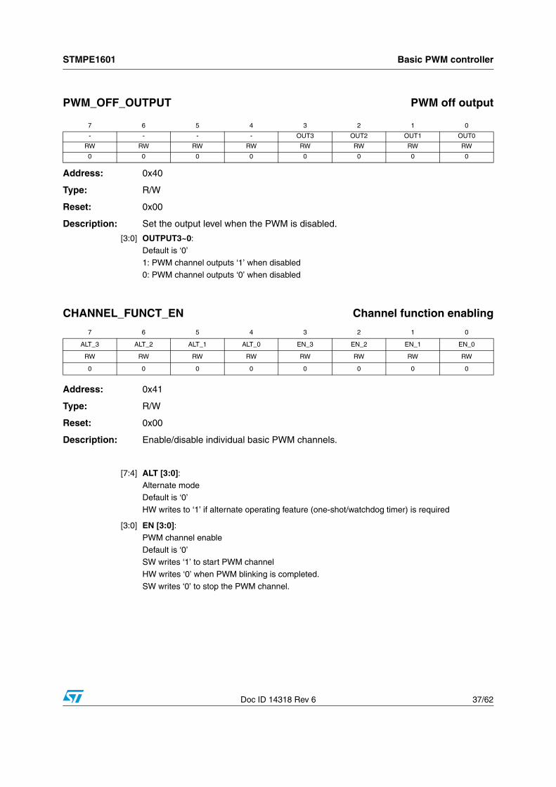
PWM_OFF_OUTPUT PWM off output
Address: 0x40
Type: R/W
Reset: 0x00
Description: Set the output level when the PWM is disabled.
CHANNEL_FUNCT_EN Channel function enabling
Address: 0x41
Type: R/W
Reset: 0x00
Description: Enable/disable individual basic PWM channels.
7 6 5 4 3 2 1 0
- - - - OUT3 OUT2 OUT1 OUT0
RW RW RW RW RW RW RW RW
0 0 0 0 0 0 0 0
[3:0] OUTPUT3~0:
Default is ‘0’
1: PWM channel outputs ‘1’ when disabled0: PWM channel outputs ‘0’ when disabled
7 6 5 4 3 2 1 0
ALT_3 ALT_2 ALT_1 ALT_0 EN_3 EN_2 EN_1 EN_0
RW RW RW RW RW RW RW RW
0 0 0 0 0 0 0 0
[7:4] ALT [3:0]:Alternate modeDefault is ‘0’
HW writes to ‘1’ if alternate operating feature (one-shot/watchdog timer) is required
[3:0] EN [3:0]:PWM channel enable
Default is ‘0’SW writes ‘1’ to start PWM channel
HW writes ‘0’ when PWM blinking is completed.
SW writes ‘0’ to stop the PWM channel.
Basic PWM controller STMPE1601
38/62 Doc ID 14318 Rev 6
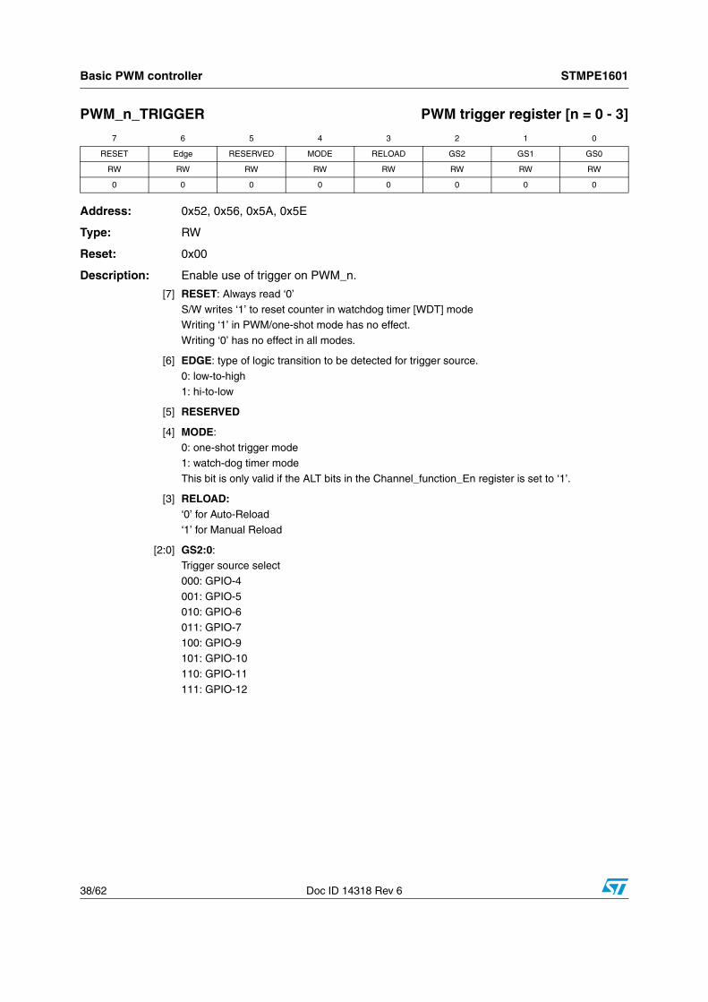
PWM_n_TRIGGER PWM trigger register [n = 0 - 3]
Address: 0x52, 0x56, 0x5A, 0x5E
Type: RW
Reset: 0x00
Description: Enable use of trigger on PWM_n.
7 6 5 4 3 2 1 0
RESET Edge RESERVED MODE RELOAD GS2 GS1 GS0
RW RW RW RW RW RW RW RW
0 0 0 0 0 0 0 0
[7] RESET: Always read ‘0’
S/W writes ‘1’ to reset counter in watchdog timer [WDT] modeWriting ‘1’ in PWM/one-shot mode has no effect.
Writing ‘0’ has no effect in all modes.
[6] EDGE: type of logic transition to be detected for trigger source.
0: low-to-high
1: hi-to-low
[5] RESERVED
[4] MODE: 0: one-shot trigger mode
1: watch-dog timer mode
This bit is only valid if the ALT bits in the Channel_function_En register is set to ‘1’.
[3] RELOAD:‘0’ for Auto-Reload‘1’ for Manual Reload
[2:0] GS2:0: Trigger source select
000: GPIO-4
001: GPIO-5010: GPIO-6
011: GPIO-7
100: GPIO-9101: GPIO-10
110: GPIO-11
111: GPIO-12
STMPE1601 Basic PWM controller
Doc ID 14318 Rev 6 39/62
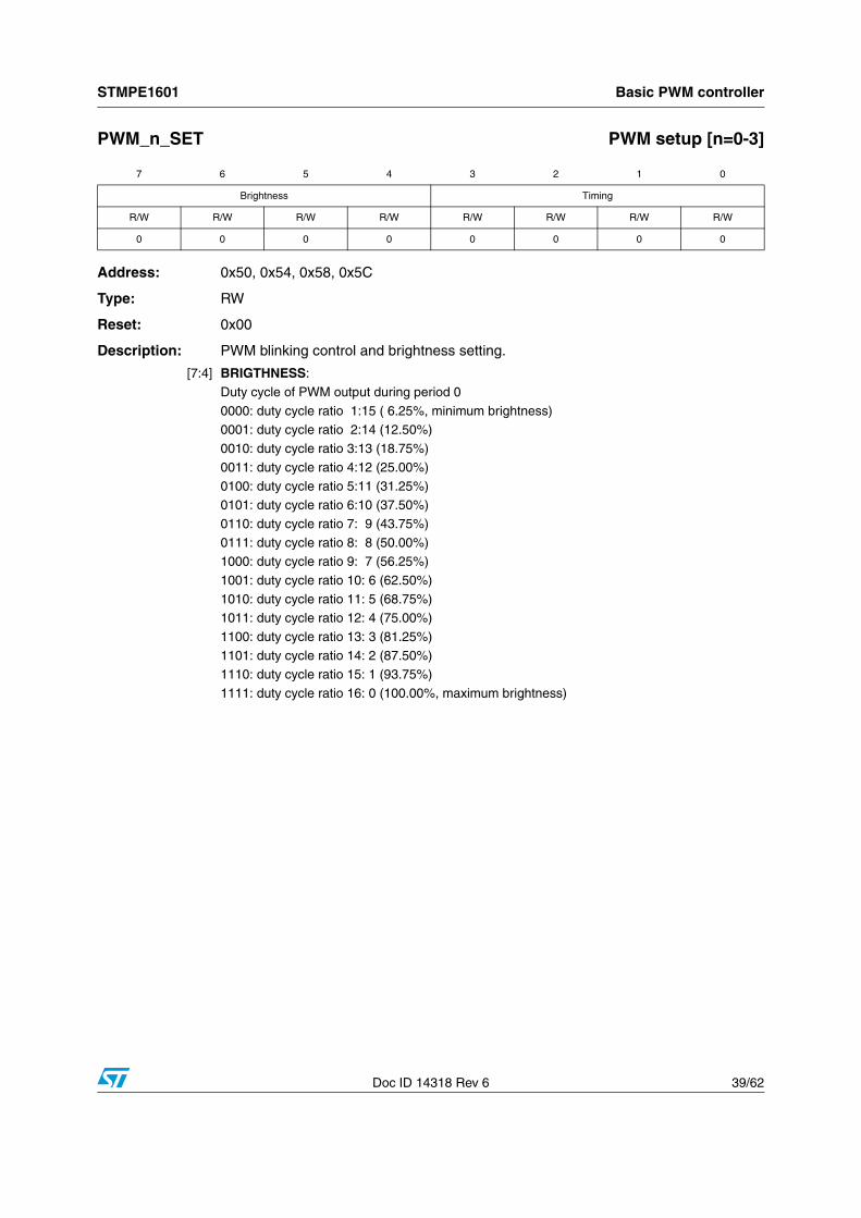
PWM_n_SET PWM setup [n=0-3]
Address: 0x50, 0x54, 0x58, 0x5C
Type: RW
Reset: 0x00
Description: PWM blinking control and brightness setting.
7 6 5 4 3 2 1 0
Brightness Timing
R/W R/W R/W R/W R/W R/W R/W R/W
0 0 0 0 0 0 0 0
[7:4] BRIGTHNESS:
Duty cycle of PWM output during period 0
0000: duty cycle ratio 1:15 ( 6.25%, minimum brightness)0001: duty cycle ratio 2:14 (12.50%)
0010: duty cycle ratio 3:13 (18.75%)
0011: duty cycle ratio 4:12 (25.00%)
0100: duty cycle ratio 5:11 (31.25%)0101: duty cycle ratio 6:10 (37.50%)
0110: duty cycle ratio 7: 9 (43.75%)
0111: duty cycle ratio 8: 8 (50.00%)1000: duty cycle ratio 9: 7 (56.25%)
1001: duty cycle ratio 10: 6 (62.50%)
1010: duty cycle ratio 11: 5 (68.75%)1011: duty cycle ratio 12: 4 (75.00%)
1100: duty cycle ratio 13: 3 (81.25%)
1101: duty cycle ratio 14: 2 (87.50%)1110: duty cycle ratio 15: 1 (93.75%)
1111: duty cycle ratio 16: 0 (100.00%, maximum brightness)
Basic PWM controller STMPE1601
40/62 Doc ID 14318 Rev 6
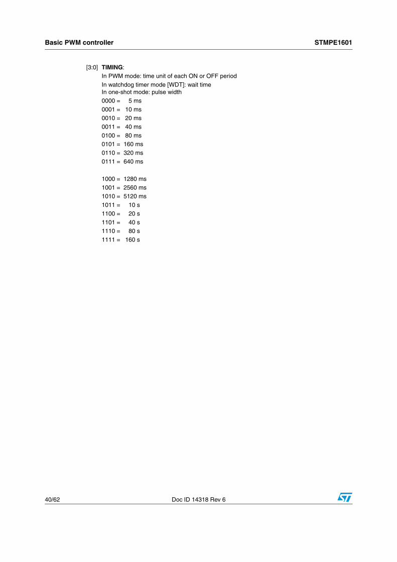
[3:0] TIMING:In PWM mode: time unit of each ON or OFF period
In watchdog timer mode [WDT]: wait timeIn one-shot mode: pulse width
0000 = 5 ms
0001 = 10 ms0010 = 20 ms
0011 = 40 ms
0100 = 80 ms0101 = 160 ms
0110 = 320 ms
0111 = 640 ms
1000 = 1280 ms
1001 = 2560 ms1010 = 5120 ms
1011 = 10 s
1100 = 20 s
1101 = 40 s1110 = 80 s
1111 = 160 s

STMPE1601 Basic PWM controller
Doc ID 14318 Rev 6 41/62
PWM_n_CTRL PWM control register [n=0-3]
Address: 0x51, 0x55, 0x59, 0x5D
Type: R/W
Reset: 0x00
Description: PWM blinking control register
7 6 5 4 3 2 1 0
Period 0 Period 1 Repetition INT_EN FRAME
RW RW RW RW RW RW RW RW
0 0 0 0 0 0 0 0
[7:6] Period 0:
1-4 time units of period 0Total length of period 0: (period 0 [1:0] + 1) * TIMING
[5:4] Period 1:0-3 time units of period 1
Total length of period 1: (period 0 [1:0]) * TIMING
[3:2] Repetition:Number of repetition
0 for Infinite repetition
[1] INT_EN:
“0” to disable interrupt generation on completion of sequence
“1” to enable interrupt generation on completion of sequence
[0] FRAME:
‘0’ will output period 0 first‘1’ will output period 1 first
Basic PWM controller STMPE1601
42/62 Doc ID 14318 Rev 6
11.1 Interrupt on basic PWM controllerA basic PWM controller can be programmed to generate interrupts at the completion of a blinking sequence. However, there are some limitations:
a) Each basic PWM controller has its own bit in the interrupt enable/status registers.
b) If enabled, the completion in any of the PWM controller triggers interrupts. No interrupt will be generated if infinite repetition is set.
c) In watchdog timer mode [WDT] , an interrupt is generated when timeout occurs
d) In “one-shot” mode, if “auto-reload”, an interrupt is generated every time a valid trigger is detected. If “non-auto-reload”, an interrupt is generated just once.
11.2 Trigger featureThe basic PWM controller can be programmed to be controlled by an external “trigger” signal. This feature can be used to implement:
– One-shot trigger circuits
– Watchdog timers
In one-shot trigger mode, a single pulse whose length is defined by TIMING[3:0] is sent to the PWM output, when a level transition is detected at the trigger source.
In watchdog mode, a 120 μs pulse is generated at the PWM output when the programmed timer has elapsed without getting any trigger for the trigger source.
STMPE1601 Keypad controller
Doc ID 14318 Rev 6 43/62
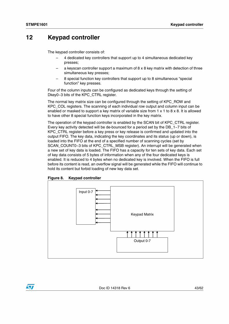
12 Keypad controller
The keypad controller consists of:
– 4 dedicated key controllers that support up to 4 simultaneous dedicated key presses;
– a keyscan controller support a maximum of 8 x 8 key matrix with detection of three simultaneous key presses;
– 8 special function key controllers that support up to 8 simultaneous “special function” key presses.
Four of the column inputs can be configured as dedicated keys through the setting of Dkey0~3 bits of the KPC_CTRL register.
The normal key matrix size can be configured through the setting of KPC_ROW and KPC_COL registers. The scanning of each individual row output and column input can be enabled or masked to support a key matrix of variable size from 1 x 1 to 8 x 8. It is allowed to have other 8 special function keys incorporated in the key matrix.
The operation of the keypad controller is enabled by the SCAN bit of KPC_CTRL register. Every key activity detected will be de-bounced for a period set by the DB_1~7 bits of KPC_CTRL register before a key press or key release is confirmed and updated into the output FIFO. The key data, indicating the key coordinates and its status (up or down), is loaded into the FIFO at the end of a specified number of scanning cycles (set by SCAN_COUNT0~3 bits of KPC_CTRL_MSB register). An interrupt will be generated when a new set of key data is loaded. The FIFO has a capacity for ten sets of key data. Each set of key data consists of 5 bytes of information when any of the four dedicated keys is enabled. It is reduced to 4 bytes when no dedicated key is involved. When the FIFO is full before its content is read, an overflow signal will be generated while the FIFO will continue to hold its content but forbid loading of new key data set.
Figure 8. Keypad controller
Input 0-7
Output 0-7
Keypad Matrix
Keypad controller STMPE1601
44/62 Doc ID 14318 Rev 6
The keypad column inputs enabled by the KPC_col register are normally 'high', with the corresponding input pins pulled up by resistors internally. After reset, all the keypad row outputs enabled by the KPC_row register are driven 'low'. If a key is pressed, its corresponding column input will become 'low' after making contact with the 'low' voltage on its corresponding row output.
Once the keyscan controller senses a 'low' input on any of the column inputs, the scanning cycles will then start to determine the exact key that has been pressed. The eight row outputs will be driven 'low' one by one during each scanning cycle. While one row is driven 'low', all other rows are in tri-state and pulled up. If there is any column input sensed as 'low' when a row is driven 'low', the key scan controller will then decode the key coordinates (its corresponding row number and column number), save the key data into a de-bounce buffer if available, confirm if it is a valid key press after de-bouncing, and update the key data into output data FIFO if valid.
12.1 Keypad configurationsThe keypad controller supports the following types of keys:
● Up to 8 input * 8 output matrix keys
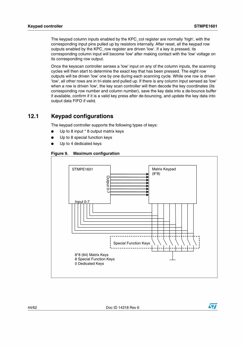
● Up to 8 special function keys
● Up to 4 dedicated keys
Figure 9. Maximum configuration
STMPE1601 Matrix Keypad (8*8) O
utput 0-7
Input 0-7
Special Function Keys
8*8 (64) Matrix Keys8 Special Function Keys 0 Dedicated Keys
STMPE1601 Keypad controller
Doc ID 14318 Rev 6 45/62
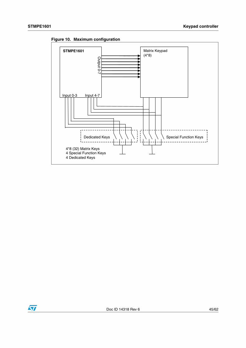
Figure 10. Maximum configuration
STMPE1601 Matrix Keypad(4*8) O
utput 0-7
Input 4-7
Special Function Keys
4*8 (32) Matrix Keys 4 Special Function Keys 4 Dedicated Keys
Dedicated Keys
Input 0-3
Keypad controller STMPE1601
46/62 Doc ID 14318 Rev 6
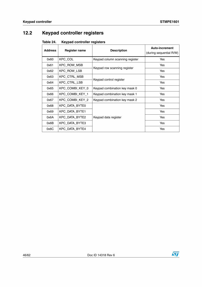
12.2 Keypad controller registers
Table 24. Keypad controller registers
Address Register name DescriptionAuto-increment
(during sequential R/W)
0x60 KPC_COL Keypad column scanning register Yes
0x61 KPC_ROW_MSBKeypad row scanning register
Yes
0x62 KPC_ROW_LSB Yes
0x63 KPC_CTRL_MSBKeypad control register
Yes
0x64 KPC_CTRL_LSB Yes
0x65 KPC_COMBI_KEY_0 Keypad combination key mask 0 Yes
0x66 KPC_COMBI_KEY_1 Keypad combination key mask 1 Yes
0x67 KPC_COMBI_KEY_2 Keypad combination key mask 2 Yes
0x68 KPC_DATA_BYTE0
Keypad data register
Yes
0x69 KPC_DATA_BYTE1 Yes
0x6A KPC_DATA_BYTE2 Yes
0x6B KPC_DATA_BYTE3 Yes
0x6C KPC_DATA_BYTE4 Yes
STMPE1601 Keypad controller
Doc ID 14318 Rev 6 47/62
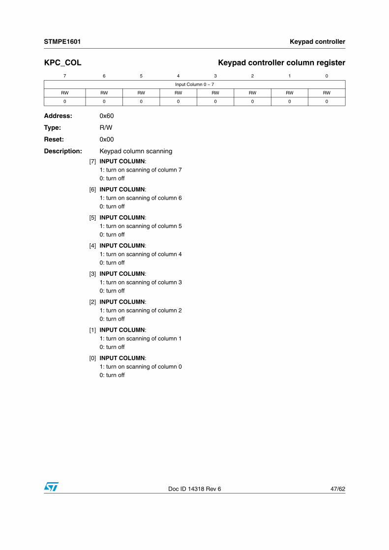
KPC_COL Keypad controller column register
Address: 0x60
Type: R/W
Reset: 0x00
Description: Keypad column scanning
7 6 5 4 3 2 1 0
Input Column 0 ~ 7
RW RW RW RW RW RW RW RW
0 0 0 0 0 0 0 0
[7] INPUT COLUMN:
1: turn on scanning of column 7 0: turn off
[6] INPUT COLUMN:1: turn on scanning of column 6
0: turn off
[5] INPUT COLUMN:1: turn on scanning of column 5
0: turn off
[4] INPUT COLUMN:
1: turn on scanning of column 4
0: turn off
[3] INPUT COLUMN:
1: turn on scanning of column 3 0: turn off
[2] INPUT COLUMN:1: turn on scanning of column 2
0: turn off
[1] INPUT COLUMN:
1: turn on scanning of column 1
0: turn off
[0] INPUT COLUMN:
1: turn on scanning of column 0 0: turn off
Keypad controller STMPE1601
48/62 Doc ID 14318 Rev 6
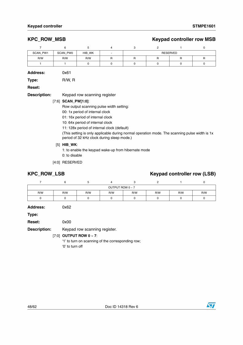
KPC_ROW_MSB Keypad controller row MSB
Address: 0x61
Type: R/W, R
Reset:
Description: Keypad row scanning register
KPC_ROW_LSB Keypad controller row (LSB)
Address: 0x62
Type:
Reset: 0x00
Description: Keypad row scanning register.
7 6 5 4 3 2 1 0
SCAN_PW1 SCAN_PW0 HIB_WK - RESERVED
R/W R/W R/W R R R R R
1 1 0 0 0 0 0 0
[7:6] SCAN_PW[1:0]:Row output scanning pulse width setting:00: 1x period of internal clock
01: 16x period of internal clock
10: 64x period of internal clock
11: 128x period of internal clock (default)(This setting is only applicable during normal operation mode. The scanning pulse width is 1x period of 32 kHz clock during sleep mode.)
[5] HIB_WK:
1: to enable the keypad wake-up from hibernate mode 0: to disable
[4:0] RESERVED
7 6 5 4 3 2 1 0
OUTPUT ROW 0 ~ 7
R/W R/W R/W R/W R/W R/W R/W R/W
0 0 0 0 0 0 0 0
[7:0] OUTPUT ROW 0 ~ 7:
‘1’ to turn on scanning of the corresponding row; ‘0’ to turn off
STMPE1601 Keypad controller
Doc ID 14318 Rev 6 49/62
KPC_CTRL_MSB Keypad controller control (MSB)
Address: 0x63
Type: R/W
Reset: 0x00
Description: Keypad control register.
KPC_CTRL_LSB Keypad controller control (LSB)
Address: 0x64
Type: R/W
Reset: 0x00
Description: Keypad control register.
7 6 5 4 3 2 1 0
SCAN_COUNT_0 ~ 3 DKEYy_0 ~ 3
RW RW RW RW RW RW RW RW
0 0 0 0 0 0 0 0
[7:4] SCAN_COUNT_0~ 3:
Number of key scanning cycles elapsed before a confirmed key data is updated into output data FIFO (0 ~ 15 cycles)
[3] DKEY_3:
Set ‘1’ to use input column 3 as dedicated key
[2] DKEY_2:Set ‘1’ to use input column 2 as dedicated key
[1] DKEY_1:Set ‘1’ to use input column 1 as dedicated key
[0] DKEY_0:Set ‘1’ to use input column 0 as dedicated key
7 6 5 4 3 2 1 0
DB[6:0] SCAN
R/W R/W R/W R/W R/W R/W R/W R/W
0 0 0 0 0 0 0 0
[7:1] DB_6:0:0-128 ms of de-bounce time
[0] SCAN:1: to start scanning
0: to stop
Data registers STMPE1601
50/62 Doc ID 14318 Rev 6
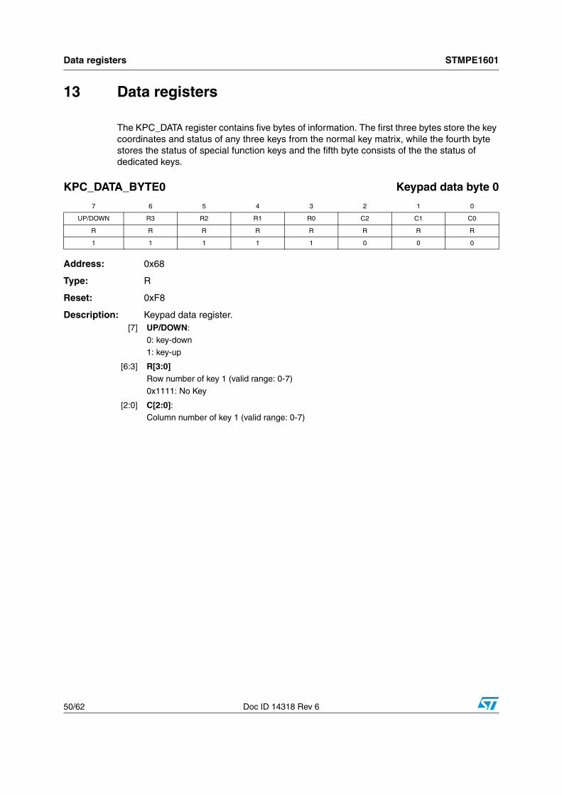
13 Data registers
The KPC_DATA register contains five bytes of information. The first three bytes store the key coordinates and status of any three keys from the normal key matrix, while the fourth byte stores the status of special function keys and the fifth byte consists of the the status of dedicated keys.
KPC_DATA_BYTE0 Keypad data byte 0
Address: 0x68
Type: R
Reset: 0xF8
Description: Keypad data register.
7 6 5 4 3 2 1 0
UP/DOWN R3 R2 R1 R0 C2 C1 C0
R R R R R R R R
1 1 1 1 1 0 0 0
[7] UP/DOWN:
0: key-down 1: key-up
[6:3] R[3:0] Row number of key 1 (valid range: 0-7)
0x1111: No Key
[2:0] C[2:0]:Column number of key 1 (valid range: 0-7)

STMPE1601 Data registers
Doc ID 14318 Rev 6 51/62
KPC_DATA_BYTE1 Keypad data byte 1
Address: 0x69
Type: R
Reset: 0xF8
Description: Keypad data register.
KPC_DATA_BYTE2 Keypad data byte 2
Address: 0x6A
Type: R
Reset: 0xF8
Description: Keypad data register.
KPC_DATA_BYTE3 Keypad data byte 3
7 6 5 4 3 2 1 0
Up/Down R3 R2 R1 R0 C2 C1 C0
R R R R R R R R
1 1 1 1 1 0 0 0
[7] UP/DOWN:
0: key-down 1: key-up
[6:3] R[3:0] Row number of key 2 (valid range: 0-7)
0x1111: No key
[2:0] C[2:0]:Column number of key 2 (valid range: 0-7)
7 6 5 4 3 2 1 0
UP/DOWN R3 R2 R1 R0 C2 C1 C0
R R R R R R R R
1 1 1 1 1 0 0 0
[7] UP/DOWN:0: key-down
1: key-up
[6:3] R[3:0] Row number of key 3 (valid range: 0 - 7)
0x1111: No key
[2:0] C[2:0]:column number of key 3 (valid range: 0 -7)
7 6 5 4 3 2 1 0
SF7 SF6 SF5 SF4 SF3 SF2 SF1 SF0
R R R R R R R R
1 1 1 1 1 1 1 1

Data registers STMPE1601
52/62 Doc ID 14318 Rev 6
Address: 0x6B
Type: R
Reset: 0xFF
Description: Keypad data register.
KPC_DATA_BYTE4 Keypad data byte 4
Address: 0x6C
Type: R
Reset: 0x0F
Description: Keypad data register.
[7:0] SF[7:0]:0: key-down
1: key-up
7 6 5 4 3 2 1 0
RESERVED Dedicated Key 0 ~ 3
R R R R R R R R
0 0 0 0 1 1 1 1
[7:4] RESERVED
[3:0] Dedicated key [3:0]:0: key-down 1 key-up
STMPE1601 Keypad combination key registers
Doc ID 14318 Rev 6 53/62
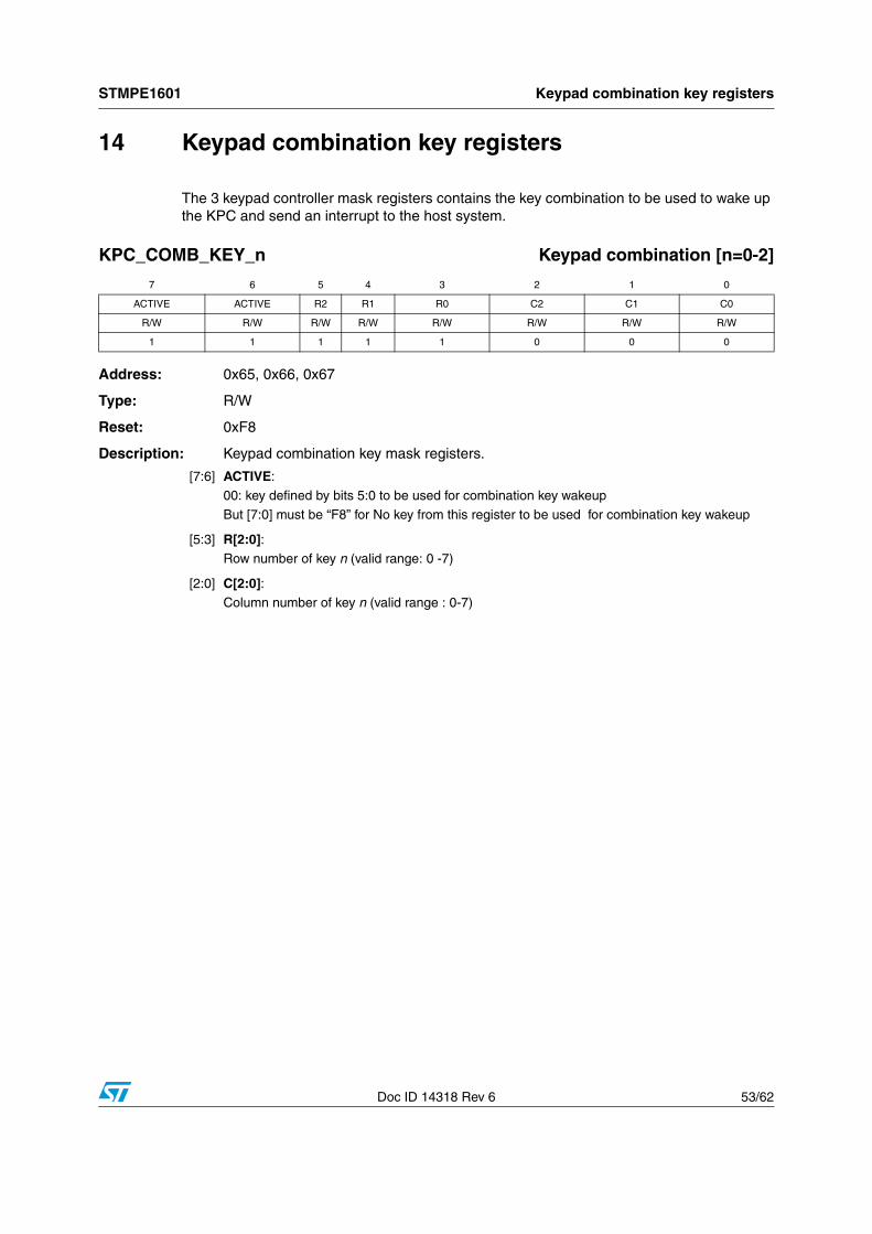
14 Keypad combination key registers
The 3 keypad controller mask registers contains the key combination to be used to wake up the KPC and send an interrupt to the host system.
KPC_COMB_KEY_n Keypad combination [n=0-2]
Address: 0x65, 0x66, 0x67
Type: R/W
Reset: 0xF8
Description: Keypad combination key mask registers.
7 6 5 4 3 2 1 0
ACTIVE ACTIVE R2 R1 R0 C2 C1 C0
R/W R/W R/W R/W R/W R/W R/W R/W
1 1 1 1 1 0 0 0
[7:6] ACTIVE:
00: key defined by bits 5:0 to be used for combination key wakeup
But [7:0] must be “F8” for No key from this register to be used for combination key wakeup
[5:3] R[2:0]:Row number of key n (valid range: 0 -7)
[2:0] C[2:0]:Column number of key n (valid range : 0-7)
Keypad combination key registers STMPE1601
54/62 Doc ID 14318 Rev 6
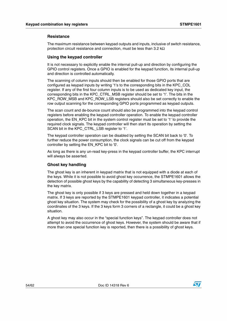
Resistance
The maximum resistance between keypad outputs and inputs, inclusive of switch resistance, protection circuit resistance and connection, must be less than 3.2 kΩ
Using the keypad controller
It is not necessary to explicitly enable the internal pull-up and direction by configuring the GPIO control registers. Once a GPIO is enabled for the keypad function, its internal pull-up and direction is controlled automatically.
The scanning of column inputs should then be enabled for those GPIO ports that are configured as keypad inputs by writing '1's to the corresponding bits in the KPC_COL register. If any of the first four column inputs is to be used as dedicated key input, the corresponding bits in the KPC_CTRL_MSB register should be set to '1'. The bits in the KPC_ROW_MSB and KPC_ROW_LSB registers should also be set correctly to enable the row output scanning for the corresponding GPIO ports programmed as keypad outputs.
The scan count and de-bounce count should also be programmed into the keypad control registers before enabling the keypad controller operation. To enable the keypad controller operation, the EN_KPC bit in the system control register must be set to '1' to provide the required clock signals. The keypad controller will then start its operation by setting the SCAN bit in the KPC_CTRL_LSB register to '1'.
The keypad controller operation can be disabled by setting the SCAN bit back to '0'. To further reduce the power consumption, the clock signals can be cut off from the keypad controller by setting the EN_KPC bit to '0'.
As long as there is any un-read key-press in the keypad controller buffer, the KPC interrupt will always be asserted.
Ghost key handling
The ghost key is an inherent in keypad matrix that is not equipped with a diode at each of the keys. While it is not possible to avoid ghost key occurrence, the STMPE1601 allows the detection of possible ghost keys by the capability of detecting 3 simultaneous key-presses in the key matrix.
The ghost key is only possible if 3 keys are pressed and held down together in a keypad matrix. If 3 keys are reported by the STMPE1601 keypad controller, it indicates a potential ghost key situation. The system may check for the possibility of a ghost key by analyzing the coordinates of the 3 keys. If the 3 keys form 3 corners of a rectangle, it could be a ghost key situation.
A ghost key may also occur in the “special function keys”. The keypad controller does not attempt to avoid the occurrence of ghost keys. However, the system should be aware that if more than one special function key is reported, then there is a possibility of ghost keys.
STMPE1601 Keypad combination key registers
Doc ID 14318 Rev 6 55/62
Key detection priority
A dedicated key is always detected, if this is enabled. When a special function key is detected, the matrix key scanning on the same input line is disabled.
Up to 3 matrix keys can be detected. Matrix keys that fall on activated special function keys are not counted.
As a result of these priority rules, a matrix key is ignored by the keypad controller when the special function key on the same input line is detected, even if the matrix key is being pressed down before the special function key. Hence, when a matrix is reported "key-down" and it is being held down while the corresponding special function is being pressed, a "no-key" status will be reported for the matrix key when the special function key is reported "key-down". If the matrix key is released while the special function key is still being held down, no "key-up" will be reported for the matrix key. On the other hand, if the matrix key is released after the special function key is reported "key-up", then a new "key-down" will be reported for the matrix key, followed by "key-up".
Keypad wakeup from sleep and hibernate modes
The keypad controller is functional in sleep mode as long as it is enabled before entering the sleep mode. It will then wake the system up into operational mode if a valid key press is detected.
In the case of hibernate mode, the 'HIB_WK' bit in 'KPC_ROW_msb' register must be set to '1' in order to enable the system wakeup by means of a valid key press. When this is enabled, an asynchronous detection of the keypad column input activity is turned on during the hibernate mode. If any key activity is detected, the system is expected to enter the sleep mode temporarily to allow a debouncing of key press to take place. If a valid key is detected, the system will then wake up into operational mode; otherwise, the device will go back into hibernate mode.
Keypad controller combination-key interrupt
The keypad controller (KPC) can be programmed to wake up from sleep mode if a unique combination keys is detected. This combination keys of up to 3 keys is specified in the KPC combination set 0-2 registers. Note that the sequence of the key pressed is not relevant, as long as the 1-3 keys specified in the KPC_COMB_KEY registers are detected, the KPC will wake up and interrupt the host.
If any other keys (beside those specified in the KPC_COMB_KEY_N registers) are pressed, it would be considered an invalid combination and no interrupt will be generated.
All the "active" keys must be pressed and held together, for the combi-key interrupt to be generated.

Miscellaneous features STMPE1601
56/62 Doc ID 14318 Rev 6
15 Miscellaneous features
15.1 ResetThe STMPE1601 is equipped with an internal POR circuit that holds the device in reset state, until the clock is steady and VCC input is valid. The host system may choose to reset the STMPE1601 by asserting the RESET_N pin.

STMPE1601 Package mechanical data
Doc ID 14318 Rev 6 57/62
16 Package mechanical data
In order to meet environmental requirements, ST offers these devices in different grades of ECOPACK® packages, depending on their level of environmental compliance. ECOPACK® specifications, grade definitions and product status are available at: www.st.com. ECOPACK® is an ST trademark.
Package mechanical data STMPE1601
58/62 Doc ID 14318 Rev 6
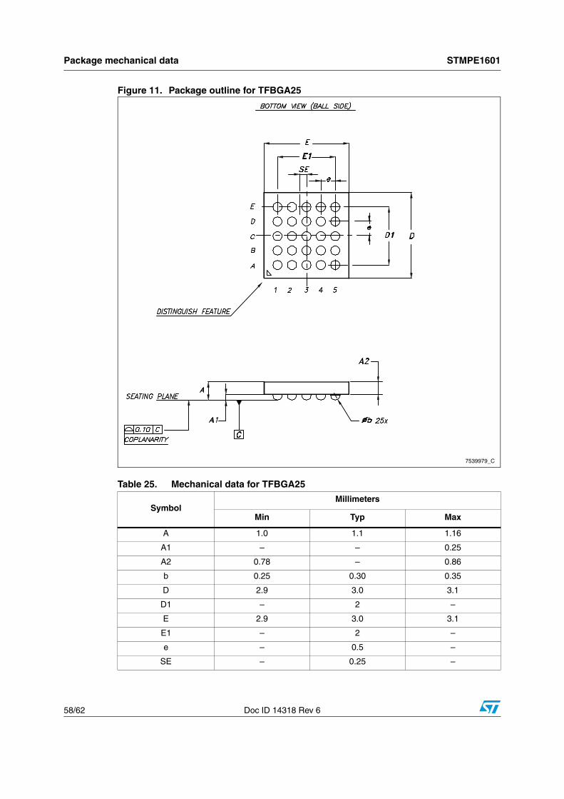
Figure 11. Package outline for TFBGA25
Table 25. Mechanical data for TFBGA25
SymbolMillimeters
Min Typ Max
A 1.0 1.1 1.16
A1 – – 0.25
A2 0.78 – 0.86
b 0.25 0.30 0.35
D 2.9 3.0 3.1
D1 – 2 –
E 2.9 3.0 3.1
E1 – 2 –
e – 0.5 –
SE – 0.25 –
7539979_C
STMPE1601 Package mechanical data
Doc ID 14318 Rev 6 59/62
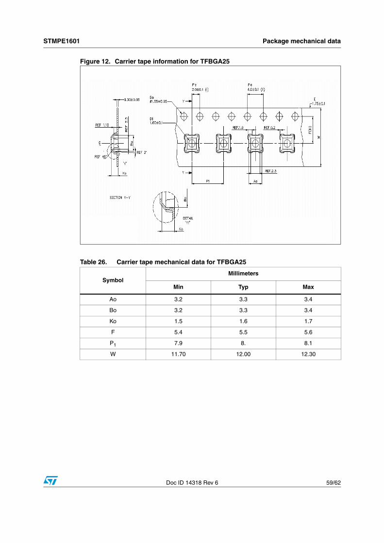
Figure 12. Carrier tape information for TFBGA25
Table 26. Carrier tape mechanical data for TFBGA25
Symbol Millimeters
Min Typ Max
Ao 3.2 3.3 3.4
Bo 3.2 3.3 3.4
Ko 1.5 1.6 1.7
F 5.4 5.5 5.6
P1 7.9 8. 8.1
W 11.70 12.00 12.30

Package mechanical data STMPE1601
60/62 Doc ID 14318 Rev 6
Figure 13. Reel drawing for TFBGA25
Table 27. Tape and reel dimensions for TFBGA25 (12 mm width)
SymbolMillimeters
Min Typ Max
N 173 178 183
W1 - 12.4 12.6
W2 - - 18.4
C 12.75 13 13.25

STMPE1601 Revision history
Doc ID 14318 Rev 6 61/62
17 Revision history
Table 28. Document revision history
Date Revision Changes
10-Jan-2008 1 Initial release.
15-Feb-2008 2
Modified Figure 1 on page 4, added info on register Description: on page 41 and Section 6.1: Minimizing current drain on I2C address lines on page 13, updated Table 7: DC electrical characteristics on page 9, minor text changes.
14-Mar-2008 3 Updated Table 7: DC electrical characteristics on page 9
02-June-2008 4
Document status promoted from preliminary data to datasheet. Modified: Figure 1 on page 4, Rup values in Table 10, Channel function enabling and PWM trigger register [n = 0 - 3] registers.
Updated: Section 6: I2C interface, Section 7: System controller, Section 9: Interrupt system, Section 10: GPIO controller, Section 11: Basic PWM controller, Section 12: Keypad controller
10-Nov-2008 5Content reworked to improve readability.
Updated: keypad controller data registers description, package, carrier tape and reel information.
01-Feb-2010 6
Modified: renamed μTFBGA25 to TFBGA25, Figure 1 on page 4, Table 19: GPIO controller (Base address = 0 x 80) on page 31,Updated: Table 2: Pin assignment on page 5, Table 11: Register map summary table on page 11, Section 7: System controller
STMPE1601
62/62 Doc ID 14318 Rev 6
Please Read Carefully:
Information in this document is provided solely in connection with ST products. STMicroelectronics NV and its subsidiaries (“ST”) reserve theright to make changes, corrections, modifications or improvements, to this document, and the products and services described herein at anytime, without notice.
All ST products are sold pursuant to ST’s terms and conditions of sale.
Purchasers are solely responsible for the choice, selection and use of the ST products and services described herein, and ST assumes noliability whatsoever relating to the choice, selection or use of the ST products and services described herein.
No license, express or implied, by estoppel or otherwise, to any intellectual property rights is granted under this document. If any part of thisdocument refers to any third party products or services it shall not be deemed a license grant by ST for the use of such third party productsor services, or any intellectual property contained therein or considered as a warranty covering the use in any manner whatsoever of suchthird party products or services or any intellectual property contained therein.
UNLESS OTHERWISE SET FORTH IN ST’S TERMS AND CONDITIONS OF SALE ST DISCLAIMS ANY EXPRESS OR IMPLIEDWARRANTY WITH RESPECT TO THE USE AND/OR SALE OF ST PRODUCTS INCLUDING WITHOUT LIMITATION IMPLIEDWARRANTIES OF MERCHANTABILITY, FITNESS FOR A PARTICULAR PURPOSE (AND THEIR EQUIVALENTS UNDER THE LAWSOF ANY JURISDICTION), OR INFRINGEMENT OF ANY PATENT, COPYRIGHT OR OTHER INTELLECTUAL PROPERTY RIGHT.
UNLESS EXPRESSLY APPROVED IN WRITING BY AN AUTHORIZED ST REPRESENTATIVE, ST PRODUCTS ARE NOTRECOMMENDED, AUTHORIZED OR WARRANTED FOR USE IN MILITARY, AIR CRAFT, SPACE, LIFE SAVING, OR LIFE SUSTAININGAPPLICATIONS, NOR IN PRODUCTS OR SYSTEMS WHERE FAILURE OR MALFUNCTION MAY RESULT IN PERSONAL INJURY,DEATH, OR SEVERE PROPERTY OR ENVIRONMENTAL DAMAGE. ST PRODUCTS WHICH ARE NOT SPECIFIED AS "AUTOMOTIVEGRADE" MAY ONLY BE USED IN AUTOMOTIVE APPLICATIONS AT USER’S OWN RISK.
Resale of ST products with provisions different from the statements and/or technical features set forth in this document shall immediately voidany warranty granted by ST for the ST product or service described herein and shall not create or extend in any manner whatsoever, anyliability of ST.
ST and the ST logo are trademarks or registered trademarks of ST in various countries.
Information in this document supersedes and replaces all information previously supplied.
The ST logo is a registered trademark of STMicroelectronics. All other names are the property of their respective owners.
© 2010 STMicroelectronics - All rights reserved
STMicroelectronics group of companies
Australia - Belgium - Brazil - Canada - China - Czech Republic - Finland - France - Germany - Hong Kong - India - Israel - Italy - Japan - Malaysia - Malta - Morocco - Philippines - Singapore - Spain - Sweden - Switzerland - United Kingdom - United States of America
www.st.com