1456 ieee transactions on components, … papers/gao - ieee_t_cpmt... · jing et al.: brittle...
TRANSCRIPT

1456 IEEE TRANSACTIONS ON COMPONENTS, PACKAGING AND MANUFACTURING TECHNOLOGY, VOL. 1, NO. 9, SEPTEMBER 2011
Brittle Versus Ductile Failure of a Lead-FreeSingle Solder Joint Specimen Under
Intermediate Strain RateJianping Jing, Feng Gao, Janine Johnson, Frank Z. Liang, Richard L. Williams, and Jianmin Qu
Abstract— The failure mode of Sn-4.0Ag–0.5Cu solder jointsunder the intermediate strain rates is explored. Tensile andshear tests were performed on miniature solder joints at twodifferent displacement rates, i.e., 5 and 50 mm/s. For the uniaxialtensile test, brittle failure occurred at the intermetallic compound(IMC)/Cu pad interface on the board side under both loadingrates. However, for shear loading at 5 mm/s, ductile failure alongthe solder matrix was detected. With the increase of the shearloading rate up to 50 mm/s, the failure mode is converted intothe (ductile + brittle) mixed mode. Numerical simulation resultsbased on the extracted elastic–plastic solder properties indicatethat the maximum stress concentration is located at the interfacesof the board side, which indicates the weak position of thecrack initiation. The plastic deformation of the solder alloy issignificantly suppressed at 50 mm/s loading rate. The amplitudeof the solder plastic deformation under shear loading is muchgreater than that for the tensile test. Furthermore, most plasticdeformation under shear loading is in the solder alloy adjacentto solder/IMC interface of the board side and no visible plasticdeformation is detected in the middle of solder ball, which resultsin cohesive failure at the rate of 5 mm/s and the (ductile + brittle)mixed failure mode at the rate of 50 mm/s.
Index Terms— Failure mode, plastic deformation, single solderjoint, Sn–4.0Ag–0.5Cu solder.
I. INTRODUCTION
NOWADAYS, Sn–Ag–Cu lead-free solders have beenconsidered as the leading candidates to replace the con-
ventional Sn–Pb solders owing to their good manufacturabil-ity, creep resistance, and thermomechanical fatigue resistance
Manuscript received March 13, 2009; revised March 14, 2011; acceptedApril 1, 2011. Date of publication August 30, 2011; date of current versionSeptember 21, 2011. This work was financially supported by Intel Corpora-tion. Recommended for publication by Associate Editor P. P. Conway uponevaluation of reviewers’ comments.
J. Jing is with the State Key Laboratory of Mechanical Systems andVibration, Shanghai JiaoTong University, Shanghai 200000, China (e-mail:[email protected]).
F. Gao and J. Qu are with the George W. Woodruff School of Mechan-ical Engineering, Georgia Institute of Technology, Atlanta, GA 30332USA. They are also with McCormick School of Engineering and AppliedScience, Northwestern University, Evanston, IL 60208 USA (e-mail: [email protected]; [email protected]).
J. Johnson was with the George W. Woodruff School of MechanicalEngineering, Georgia Institute of Technology, Atlanta, GA. She is now withthe Lincoln Laboratory, Massachusetts Institute of Technology, Lexington,MA 02421-6426 USA (e-mail: [email protected]).
F. Z. Liang and R. L. Williams are with Intel Corporation, Hillsboro, OR97124 USA (e-mail: [email protected]; [email protected]).
Color versions of one or more of the figures in this paper are availableonline at http://ieeexplore.ieee.org.
Digital Object Identifier 10.1109/TCPMT.2011.2146259
[1], [2]. However, a crucial reliability issue of the lead-free solder joints has emerged. That is, compared to Sn–Pbsolder joints, the lead-free solder joint exhibits deteriorationin performance under shock/impact loading. In the meantime,the proliferation of portable electronic devices, such as cellularphones and laptop computers, makes the drop in performanceof the solder joint very important.
The local strain rate within a solder joint at the dropcondition may differ from 1 s−1–1000 s−1, depending on thedrop height, orientation, surface rigidity, etc. [3]. For board-level drop test or single ball impact test, a number of studieshave been reported [4]–[6]. In particular, the Hopkinson barhas been utilized to explore the mechanical behavior underhigh strain rates (500–3000 s−1) [7], [8]. Recently, it has beenfound that the solder properties strongly depend on the solderjoint height [9].
This paper is devoted to the study of the properties of aminiature solder ball, which are extracted directly from theforce–displacement measurement data. The solder joint failuremode under different loading conditions is then discussed onthe basis of numerical simulation results.
II. SINGLE SOLDER JOINT (SSJ) SAMPLE PREPARATION
The package and printed circuit board (PCB) were solderedusing the commercial Sn–4.0Ag–0.5Cu (SAC405) lead-freesolder alloy. The SSJ was then made through the singulationprocess from an assembled PCB, so that the SSJ specimenmatched with the targeted ball grid array solder joint. Thedimensions of the SSJ are shown in Table I. Fig. 1 illustratesa typical SSJ that is assembled for the tensile loading test.
Intermetallic compounds (IMCs) are formed at the inter-faces of both the package and board sides, as illustrated inFig. 2(a). Several kinds of IMCs, such as block-like Cu6Sn5and needle-like Ag3Sn, are detected in the solder matrix.The formation of large-sized Ag3Sn plates is due to therelatively high initial Ag content. The (β-Sn + Ag3Sn) and(β-Sn + Ag3Sn + Cu6Sn5) eutectic phases are networked withdendrite-shaped β-Sn structures. The cross-polarized image inFig. 2(b) reveals that the solder ball consists of a limitednumber of grains with different orientations, although thepolarized image cannot detail the grain orientation as in orien-tation imaging microscopy. Accordingly, the solder alloy is anonhomogeneous microstructure and possesses several grainswith different orientations. The properties of the SAC405
2156–3950/$26.00 © 2011 IEEE

JING et al.: BRITTLE VERSUS DUCTILE FAILURE OF A LEAD-FREE SINGLE SOLDER JOINT 1457
Fig. 1. Typical SSJ assembled for testing.
TABLE I
DIMENSIONS OF SINGLE SOLDER JOINT SPECIMEN
PCB Cu pad interface diameter (μm) 450Substrate pad interface diameter (μm) 500
Solder ball diameter (μm) 550Solder joint height (μm) 355
Substrate/PCB (width × depth) (μm) 1160 × 1300
alloy in our study were carefully estimated. The followingsection describes the methodology to extract the elastic–plasticproperties of solder alloy.
A. Experimental Test Procedure
High-speed testing was carried out on a home-developedtest frame, with grips developed specifically for the SSJtest. Before testing, platens were made for easy removaland installation of the solder joints into the grips. Eachplaten consists of bottom and top with a planar surfacefor sample attachment. As illustrated in Fig. 1, the internalangles θ of these planes were 0° and 90°, where 0° corre-sponded to a uniaxial tensile test and 90° corresponded to ashear test.
After removing the debris from the solder joint, the samplewas presoaked in distilled water and then was glued onto aplaten with the substrate side down and allowed to cure for15 min. This platen was placed in the grips on the actuatorside. Then the circuit board was affixed to the opposite platenby raising the frame until the circuit board and the top platenwere connected by a thin film of glue. A second cure timeof 15 min was applied. After the actuator was started at thedesired speed, load was not applied to the solder joint untilan additional alignment cylinder on the actuator side was fullyextended. The load displacement sampling rate was 2 × 10⁻⁴ sfor 5 mm/s and 4×10⁻⁵ s for 50 mm/s, which ensured that thecontinuous force–displacement data were recorded accurately.After the test, the cross-sectional microstructure was observedby optical microscopy.
(a)
(b)
Fig. 2. Optical micrographs of a SSJ. (a) SSJ before testing. (b) Correspond-ing cross-polarized image.
B. Test Results: Force Versus Displacement Curves
The test data at two loading rates (i.e., 5 and 50 mm/s),which are shown in Fig. 3, were employed to assess themechanical properties of solder by reverse calculations. In thecalculation, the measured displacements shown in Fig. 3 wereused as prescribed loading conditions on the top surface of thespecimen, the reaction force at the bottom of the specimen wasthen calculated by numerical analysis. When the calculatedreaction forces fitted the measured forces, the mechanicalproperties of solder alloy at different loading rates were thenobtained.
Fig. 4 displays the derived properties of SAC405 solderalloy in this paper by the reverse analysis of the recordedforce–displacement data. The properties presented here wereanticipated to include several aspects, such as microstruc-ture, solder ball size effect, etc. It has been reported thatthe grain orientation in a small-size solder ball will affectthe stress and strain distributions [10]. Due to the diversesolder ball microstructures in an assembled PCB, the grainorientation effect is not specified in this paper. Overall, it canbe seen that at the higher displacement rate, namely, 50 mm/s,

1458 IEEE TRANSACTIONS ON COMPONENTS, PACKAGING AND MANUFACTURING TECHNOLOGY, VOL. 1, NO. 9, SEPTEMBER 2011
18
16
14
12
10
8
6
4
2
00 5 10
5 mm/s50 mm/s
15
Displacement (µm)
Forc
e (N
)
20 25 30 35
Fig. 3. Relation of the force versus displacement at different loading rates(5 and 50 mm/s).
200
180
160
140
120
100
80
60
40
20
0
0.00 0.02 0.04
Strain (l)
0.06 0.08
5 mm/s50 mm/s
Stre
ss (
MPa
)
Fig. 4. Derived stress versus strain relation of the solder alloy at differenttensile loading rates.
the yield strength of SAC405 solder alloy becomes greater.The Young’s modulus at 50 mm/s is also slightly elevated.This in turn affects the plastic deformation behavior of thesolder alloy, which will be addressed later. The propertieswere then adopted as the input parameters for the subsequentnumerical simulation, in order to reveal the weak position forthe potential crack initiation and propagation qualitatively ofan SSJ which was subjected to different loading conditions.
III. RESULTS AND DISCUSSION: BRITTLE VERSUS
DUCTILE FAILURE
A. Load Rate 5 mm/s
For uniaxial tensile loading at 5 mm/s, the brittle failurealong the IMC/board pad interface is dominant, as shownin Fig. 5(a) and (b). These interfaces were found to be theweak positions for the interconnections under high strainrate loading, which was partially attributed to the brittlecharacteristics of the IMCs. It is interesting that the edges ofthe fracture interface show the ductile behavior. Remarkableplastic deformation was likely to occur at these edge zones,which indicated that the crack might initiate from the triplejoint of the solder/IMC/Cu interfaces rather than from the
Package side
intefacial compound
Cu6Sn
5
Ag3Sn
0.10 mm
0.10 mm
(b)
(a)
Fig. 5. Microstructure of solder joint at package side after the uniaxial tensiletest (5 mm/s). (a) Package side solder joint after testing. (b) Close-up of thefracture surface.
TABLE II
ISOTROPIC MATERIAL PARAMETERS
Solder Copper SM Ni Cu6Sn5
E (GPa) 53 (50 mm/s)50 (5 mm/s)
117 24 203 119
v 0.34 0.34 0.4 0.34 0.29
IMC/Cu interface. A different failure mode took place forshear loading at 5 mm/s. Fig. 6(a) and (b) depict the fracturesurfaces at the package side and board side, respectively,which exhibit a ductile-controlling failure. Clearly, the failuredevelops along the solder alloy matrix, and the dramaticdeformation of the solder alloy also occurs at the fracturesurface.
Based on the failure mode and the microstructure obser-vation, it is inferred that the deformation of the solder alloynear the solder/IMC interface under the shear loading is moresevere than that under tensile loading. Moreover, the interfaceat the board side is more susceptible to the stress concentrationand the subsequent crack initiation. A numerical simulationwas therefore performed to seek a qualitative explanation.

JING et al.: BRITTLE VERSUS DUCTILE FAILURE OF A LEAD-FREE SINGLE SOLDER JOINT 1459
TABLE III
ANISOTROPIC MATERIAL PARAMETERS
E1, v1 (GPa, /) E2, v2 (GPa, /) E3, v3 (GPa, /) G12 (GPa) G13 (GPa) G23 (GPa)PCB 22, 0.28 22, 0.28 4.8, 0.18 8.0 4.0 4.0
Substrate 21, 0.3 21, 0.3 6.0, 0.2 8.0 4.0 4.0
(a)
(b)
Package side
Board side
IMC layer
Cu pad
solder
0.10 mm
0.10 mm
Fig. 6. Microstructure of solder joint at both sides after the shear test(5 mm/s). (a) Package side solder joint after testing. (b) Fracture surfaceat the board pad.
Fig. 7(a) depicts a 3-D SSJ model for the numericalsimulation, while Fig. 7(b) shows a close-up view of theinterfaces in an SSJ. Tables I–III display the SSJ dimensionsand material properties, while the elastic–plastic propertiesof SAC405 solder joint are governed by the plots in Fig. 4.The numerical calculation was performed using the ABAQUSsoftware. In order to simulate the loading process, the bottomsurface of an SSJ model was frozen in the x , y, and zdirections, which mimics the situation where the bottom ofthe specimen is glued to a rigid substrate. The velocities, i.e.,5 and 50 mm/s, are prescribed for all the nodes on the topsurface of a finite element system. The velocity normal to thetop surface represents a simple tensile loading (θ = 0°), while
(b)
(a)
Package side
Solder mask
Board side
Fig. 7. (a) 3-D SSJ model for the finite element simulation. (b) Close-upview of the interfaces of a SSJ.
the velocity parallel to the top surface denotes a pure sheartest (θ = 90°). It should be noted that, for shear loading, thetop and bottom surfaces are constrained to be parallel duringthe entire process to avoid any rotation, which is consistentwith the actual shear test loading condition. The IMC with afew micrometers at the board side is included in the model.The IMC is Cu6Sn5 at the board side. And the IMC layeris simplified as having a flat morphology in the simulationmodels.
Figs. 8 and 9 illustrate the stress and equivalent plastic strainfields under the uniaxial tensile and shear loading at the rateof 5 mm/s, respectively. It can be seen that for both tensile andshear loading, the maximum stress concentration is at the edgeof solder/IMC/Cu pad interfaces of the board side. Figs. 8(c)and 9(c) show the enlarged stress field at the interface domainof the board side for a clear view. At the package side, thestress concentration amplitude is much lower. This indicatesthat the solder/IMC/Cu interfaces at the board side are thepotential sites for damage initiation, which is consistent withthe experimental observation. However, the failure modes for

1460 IEEE TRANSACTIONS ON COMPONENTS, PACKAGING AND MANUFACTURING TECHNOLOGY, VOL. 1, NO. 9, SEPTEMBER 2011
(a)
(b)
(c)
Fig. 8. Simulated results for the uniaxial tensile loading (5 mm/s).(a) Equivalent plastic strain field. (b) Mises stress field. (c) Enlarged stressfield at the interface of the board side.
tensile and shear loading are quite different, which is dueto the different distributions of plastic deformation of thesolder alloy. Under the tensile loading (rate = 5 mm/s), themaximum plastic deformation is mainly located at the edge ofthe interface between the solder alloy and the IMC layer, andincreases gradually toward the solder alloy. It should be noted
(a)
(b)
(c)
Fig. 9. Simulated results for the shear loading (5 mm/s). (a) Equivalent plasticstrain field. (b) Mises stress field. (c) Enlarged stress field at the interface ofthe board side.
that, at the board side, the solder alloy adjacent to the IMClayer is not subjected to a significant plastic deformation. Forthe shear test, it is interesting that the plastic deformation ofthe solder alloy adjacent to the IMC layer is also altered. Thatis, most of the plastic zone lies on the solder alloy adjacent tothe solder/IMC interface and decreases gradually toward the

JING et al.: BRITTLE VERSUS DUCTILE FAILURE OF A LEAD-FREE SINGLE SOLDER JOINT 1461
(a)
(b)
Fig. 10. Microstructure of solder joint at both sides after the uniaxial tensileloading (50 mm/s). (a) Package side solder joint after testing. (b) Residualpad at the board side.
inner solder matrix. In the middle area of the solder alloy, thereis almost no visible plastic deformation, which in turn impliesthat it will be more effective in releasing the solder/IMCinterfacial energy by the solder alloy. In fact, this phenomenonhas been studied by the so-called extrinsic toughening, whichrefers to a toughening mechanism by the reduction of effectiveor net crack driving force that the crack tip actually expe-riences through various energy dissipation processes withoutincreasing inherent fracture resistance of material or interface[11], [12]. The extrinsic toughening is concerned with variousenergy dissipation processes in the zone surrounding thecrack to increase the energy consumed per unit extension ofcrack length. Extrinsic toughening often plays a dominantrole in the overall fracture resistance, especially for brittlematerials or an interface in which intrinsic toughening is oftenineffective.
At a solder joint, the interface fracture resistance is known tobe determined by two distinct energy-absorbing processes: thenear-crack tip work of fracture (intrinsic fracture resistance)and various energy dissipation processes in a zone surroundingthe interfacial crack [11]. The energy dissipation processes
(a)
(b)
Fig. 11. Microstructure of solder joint at both sides after the shear loading(50 mm/s). (a) Solder ball delamination at the package side. (b) Fracturesurface at the board pad.
arise from the plasticity of the adjacent ductile layer, whichtends to dissipate the applied crack driving force so that thenet driving force is reduced. It has been reported that theplastic deformation in the adjacent ductile layer has significanttoughening effects on the interface fracture [12]. In the solderjoint, this ductile layer is the solder ball, which easily showsplastic deformation under loading while the brittle material isIMC or Cu. If the solder plasticity adjacent to the IMC isenhanced, a higher resistance to interfacial crack propagationunder loading will be achieved as more energy is dissipatedby the ductile solder. Therefore, under shear loading, it willmake the crack propagation shift up to the solder matrix andresult in an entire cohesive failure within the solder alloy.This is also consistent with the experimental results shownin Fig. 6(b). In the meantime, it can be concluded that theSSJ is more susceptible to brittle interfacial fracture alongthe IMC/Cu interface under tensile loading due to the smallplastic deformation of solder alloy adjacent to the IMC layer.Although the grain orientations of solder ball may alter thestress and plastic deformation contours, our results can stillshed the light to estimate the failure mode qualitatively.
1462 IEEE TRANSACTIONS ON COMPONENTS, PACKAGING AND MANUFACTURING TECHNOLOGY, VOL. 1, NO. 9, SEPTEMBER 2011
(a)
(b)
Fig. 12. Simulated results under the uniaxial tensile loading (50 mm/s).(a) Equivalent plastic strain field. (b) Mises stress field.
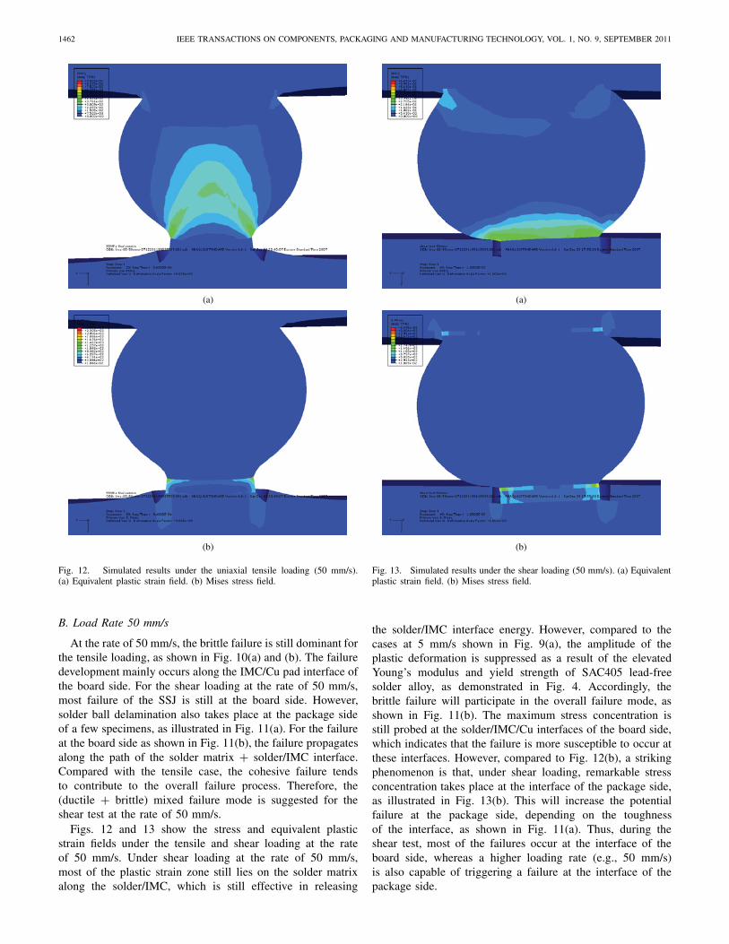
B. Load Rate 50 mm/s
At the rate of 50 mm/s, the brittle failure is still dominant forthe tensile loading, as shown in Fig. 10(a) and (b). The failuredevelopment mainly occurs along the IMC/Cu pad interface ofthe board side. For the shear loading at the rate of 50 mm/s,most failure of the SSJ is still at the board side. However,solder ball delamination also takes place at the package sideof a few specimens, as illustrated in Fig. 11(a). For the failureat the board side as shown in Fig. 11(b), the failure propagatesalong the path of the solder matrix + solder/IMC interface.Compared with the tensile case, the cohesive failure tendsto contribute to the overall failure process. Therefore, the(ductile + brittle) mixed failure mode is suggested for theshear test at the rate of 50 mm/s.
Figs. 12 and 13 show the stress and equivalent plasticstrain fields under the tensile and shear loading at the rateof 50 mm/s. Under shear loading at the rate of 50 mm/s,most of the plastic strain zone still lies on the solder matrixalong the solder/IMC, which is still effective in releasing
(a)
(b)
Fig. 13. Simulated results under the shear loading (50 mm/s). (a) Equivalentplastic strain field. (b) Mises stress field.
the solder/IMC interface energy. However, compared to thecases at 5 mm/s shown in Fig. 9(a), the amplitude of theplastic deformation is suppressed as a result of the elevatedYoung’s modulus and yield strength of SAC405 lead-freesolder alloy, as demonstrated in Fig. 4. Accordingly, thebrittle failure will participate in the overall failure mode, asshown in Fig. 11(b). The maximum stress concentration isstill probed at the solder/IMC/Cu interfaces of the board side,which indicates that the failure is more susceptible to occur atthese interfaces. However, compared to Fig. 12(b), a strikingphenomenon is that, under shear loading, remarkable stressconcentration takes place at the interface of the package side,as illustrated in Fig. 13(b). This will increase the potentialfailure at the package side, depending on the toughnessof the interface, as shown in Fig. 11(a). Thus, during theshear test, most of the failures occur at the interface of theboard side, whereas a higher loading rate (e.g., 50 mm/s)is also capable of triggering a failure at the interface of thepackage side.

JING et al.: BRITTLE VERSUS DUCTILE FAILURE OF A LEAD-FREE SINGLE SOLDER JOINT 1463
IV. CONCLUSION
The failure behavior of an SSJ was explored on the basisof microstructural observation and the numerical simulation.The following conclusions could be arrived at:
1) the SAC405 lead-free solder alloy properties exhibitstrong dependence on the loading rates. The propertieswere extracted here on the basis of the in situ testing,which included the contributions of both the microstruc-ture and the solder ball size effects. Overall, at higherloading rates (e.g., 50 mm/s), greater Young’s modulusand yield strength were achieved;
2) the SSJ subjected to tensile or shear loading showsdifferent failure modes. For uniaxial tensile loading, thebrittle failure at the interface of board side is dominantunder the rates of 5 and 50 mm/s. However, for the sheartesting, it is converted into cohesive failure mode at therate of 5 mm/s, whereas the failure develops along thepath of solder matrix + solder/IMC at the loading rateof 50 mm/s due to the higher Young’s modulus and yieldstrength;
3) for all the cases discussed here, the maximum stressconcentration takes place at the interface of the boardside, which reveals the weak site of the crack initiation.In particular, compared to tensile loading, a remarkablestress concentration is also generated at the interface ofthe package side under shear loading, which enhancesthe failure possibility at the package side to some extent;
4) under uniaxial tensile loading, the maximum plasticdeformation is located at the interface edge of the boardside and decreases gradually toward the solder matrix,while the solder alloy adjacent to the solder/IMC inter-face is not subjected to significant plastic deformation.Under the shear loading, the majority of the plasticdeformation lies on the solder adjacent to the solder/IMCinterface and almost no visible plastic deformation isprobed in the middle area of the solder ball. The differentdistribution and amplitude of the solder alloy plasticdeformation are responsible for the different failuremodes of an SSJ model under tensile and shear loading.
V. ACKNOWLEDGMENT
The authors would like to thank C. Ralph for samplepreparation and test setup.
REFERENCES
[1] S. L. Choi, A. W. Gibson, J. L. McDougall, T. R. Bieler, and K. N.Subramanian, Design Reliability of Solders and Solder Interconnections,R. K. Mahidhara, D. R. Fear, and K. L. Murty, Eds. Warrendale, PA:TMS, 1977, pp. 241–245.
[2] R. W. Neu, D. T. Scott, and M. W. Woodmansee, “Thermomechanicalbehavior of 96Sn-4Ag and casting alloy,” Trans. ASME J. Electron.Packag., vol. 123, no. 3, pp. 238–246, Sep. 2001.
[3] X. Long, I. Dutta, V. Sarihan, and D. R. Frear, “Deformation behavior ofSn-3.8Ag-0.7Cu solder at intermediate strain rates: Effect of microstruc-ture and test conditions,” J. Electron. Mater., vol. 37, no. 2, pp. 189–200,2008.
[4] J.-W. Kim and S.-B. Jung, “Reexamination of the solder ball shear testfor evaluation of the mechanical joint strength,” Int. J. Solids Struct.,vol. 43, nos. 7–8, pp. 1928–1945, Apr. 2006.
[5] O. van der Sluis, R. B. R. van Silfhout, R. A. B. Engelen, W. D.van Driel, and G. Q. Zhang, “A numerical method for efficient failuremodelling of 3-D bond pad structures,” in Proc. Electron. Comp.Technol. Conf., Reno, NV, 2007, pp. 235–241.
[6] C.-L. Yeh and Y.-S. Lai, “Effects of solder alloy constitutive relation-ships on impact force responses of package-level solder joints underball impact test,” J. Electron. Mater., vol. 35, no. 10, pp. 1892–1901,2006.
[7] C. R. Siviour, D. M. Eilliamson, S. J. P. Palmer, S. M. Walley, W. G.Proud, and J. E. Field, “Dynamic properties of solders and solder joints,”J. Phys., IV, vol. 110, no. 1, pp. 477–482, Sep. 2003.
[8] K. Kaminishi, T. Sekine, T. Maruichi, and S. Osaki, “Impact tensilecharacteristics of Sn-3.0Ag-0.5 Cu lead-free solder,” Trans. Jpn. Soc.Mech. Eng., vol. 70, no. 690, pp. 266–272, 2004.
[9] P. Zimprich, U. Saeed, A. Betzwar-Kotas, B. Weiss, and H. Ipser,“Mechanical size effects in miniaturized lead-free solder joints,” J.Electron. Mater., vol. 37, no. 1, pp. 102–109, 2008.
[10] J. C. Gong, C. Q. Liu, P. P. Conway, and V. V. Silberschmidt, “Microme-chanical modelling of SnAgCu solder joint under cyclic loading: Effectof grain orientation,” Comput. Mater. Sci., vol. 39, no. 1, pp. 187–197,Mar. 2007.
[11] D. Suh, D. W. Kim, P. L. Liu, H. C. Kim, J. A. Weninger, C. M. Kumar,A. Prasad, B. W. Grimsley, and H. B. Tejada, “Effects of Ag contenton fracture resistance of Sn–Ag–Cu lead-free solders under high-strainrate conditions,” Mater. Sci. Eng.: A, vols. 460–461, pp. 595–603, Jul.2007.
[12] R. H. Dauskardt, M. Lane, Q. Ma, and N. Krishna, “Adhesion anddebonding of multilayer thin film structures,” Eng. Fract. Mech., vol. 61,no. 1, pp. 141–162, Aug. 1998.
Jianping Jing received the Ph.D. degree fromthe School of Power Machinery and Engineering,Harbin Institute of Technology, Harbin, China, in2002.
He is currently a Professor with the State Key Lab-oratory of Mechanical System and Vibration, Schoolof Mechanical and Power Engineering, ShanghaiJiaotong University, Shanghai, China. He has pub-lished more than 50 research papers. His currentresearch interests include rotor dynamics, fault diag-nosis of rotary machinery, damage and reliability of
mechanical structures, and vibration and noise control of mechanical systems.
Feng Gao received the Ph.D. degree from HarbinInstitute of Technology, Harbin, China.
He is currently a Research Associate in the Depart-ments of Civil and Environmental Engineering andMechanical Engineering, Northwestern University,Evanston, IL. His current research interests includelead-free solder alloys, reliability of interconnec-tions, and nanostructures in microelectronic pack-aging.
Janine Johnson received the Ph.D. degree in mechanical engineering fromGeorgia Institute of Technology, Atlanta, GA, in 2009.
She is currently with the Lincoln Laboratory, Massachusetts Institute ofTechnology, Lexington, where she is working on solder fatigue in electronicpackaging. Her current research interests include mechanics of materials, andspecifically studying composites used in fuel cells.

1464 IEEE TRANSACTIONS ON COMPONENTS, PACKAGING AND MANUFACTURING TECHNOLOGY, VOL. 1, NO. 9, SEPTEMBER 2011
Frank Z. Liang received the Ph.D. degree inmechanical engineering from Oregon State Univer-sity, Corvallis, in 1991.
He is a Staff Engineer in the Mechanical CoreCompetency Group, Intel Corporation, Hillsboro,OR. He has contributed extensively to the dynamicanalyses and development of mechanical shock mod-eling and testing methodologies for electronic com-ponents, circuit boards, and computer systems.
Dr. Frank is a fellow of the American Societyof Mechanical Engineers. He has been a registered
Professional Engineer since 1993.
Richard L. Williams received the M.S. degree fromWashington State University, Pullman, and the B.S.degree in applied physics from the University ofUtah, Salt Lake City.
He was the Manager of the Assembly Test andTechnology Development, Mechanical and Model-ing Group, Intel Corporation, Hillsboro, OR, over-seeing the project. He has recently transferred toIntel’s Ultra Mobility Group.
Jianmin Qu is currently a Walter P. Murphy Pro-fessor of civil and environmental engineering andmechanical engineering at Northwestern University,Evanston, IL. His current research interests includemicromechanics of composites, interfacial fractureand adhesion, fatigue and creep damage in metallicand polymer materials, thermomechanical reliabilityof microelectronic packaging, and ultrasonic nonde-structive evaluation of advanced engineering materi-als. He has authored or co-authored two books andover 140 referred journal papers and book chapters
in the above areas.