10/28/091 implementing an instruction set david e. culler cs61cl oct 28, 2009 lecture 9 ucb cs61cl...
Post on 19-Dec-2015
218 views
TRANSCRIPT
10/28/09 1
Implementing an Instruction Set
David E. Culler
CS61CL
Oct 28, 2009
Lecture 9
UCB CS61CL F09 Lec 9

10/14/09 CS61CL F09 2
Review: Synchronous Circuit Design
• clock– distributed to all flip-flops
• ALL CYCLES GO THROUGH A REG!
• Combinational Logic Blocks (CL)– Acyclic
– no internal state (no feedback)
– output only a function of inputs
• Registers (reg)– collections of flip-flops
reg regCL CL
clock input
output
option feedback
input output

MIPS: Register Transfers
10/14/09 CS61CL F09 3

MIPS: Register Transfers
10/28/09 UCB CS61CL F09 Lec 9 4

MIPS: Register Transfers
10/28/09 UCB CS61CL F09 Lec 9 5

6
A Standard High-level Organization
• Controller– accepts external and control input,
generates control and external output and sequences the movement of data in the datapath.
• Datapath– is responsible for data manipulation.
Usually includes a limited amount of storage.
• Memory– optional block used for long term
storage of data structures.
• Standard model for CPUs, micro-controllers, many other digital sub-systems.
• Usually not nested.
• Often cascaded:

7
Datapath vs Control
• Datapath: Storage, FU, interconnect sufficient to perform the desired functions
– Inputs are Control Points– Outputs are signals
• Controller: State machine to orchestrate operation on the data path
– Based on desired function and signals
Datapath Controller
Control Points
signals

8
Register Transfer Level Descriptions
• A standard high-level representation for describing systems.
• It follows from the fact that all synchronous digital system can be described as a set of state elements connected by combination logic (CL) blocks:
• RTL comprises a set of register transfers with optional operators as part of the transfer.
• Example:
regA regB
regC regA + regB
if (start==1) regA regC
• Personal style:– use “;” to separate transfers that
occur on separate cycles.
– Use “,” to separate transfers that occur on the same cycle.
• Example (2 cycles):
regA regB, regB 0;
regC regA;
reg regCL CL
clock input
output
option feedback
input output

The Methodology
1. Identify state and operations visible in the ISA– register transfer level operations of the ISA
2. Select a set of storage elements, function units, and interconnections that – realize all the “architected” state & operations
– plus internal state and operations
3. Map each instruction to register transfers on the data path
4. Identify the control points that cause the specified data transfers
5. Implement a controller that asserts those control points– as a function of instruction, controller state, and signals
from the data path
10/28/09 UCB CS61CL F09 Lec 9 9

04/18/23 cs61cl f09 lec 6 10
MIPS R3000 – tiny subset0r0
r1°°°r31PClohi
Programmable storage
2^32 x bytes
31 x 32-bit GPRs (R0=0)
32 x 32-bit FP regs (paired DP)
HI, LO, PC
Arithmetic logical Add, AddU, Sub, SubU, And, Or, Xor, Nor, SLT, SLTU, AddI, AddIU, SLTI, SLTIU, AndI, OrI, XorI, LUISLL, SRL, SRA, SLLV, SRLV, SRAV
Memory AccessLB, LBU, LH, LHU, LW, LWL,LWRSB, SH, SW, SWL, SWR
ControlJ, JAL, JR, JALRBEQ, BNE, BLEZ,BGTZ,BLTZ,BGEZ,BLTZAL,BGEZAL

TinyMIPS
• Reg-Reg instructions (op == 0)– addu R[rd] := R[rs] + R[rt]; pc:=pc+4
– subu R[rd] := R[rs] - R[rt]; pc:=pc+4
• Reg-Immed (op != 0)– lw R[rt] := Mem[ R[ rs ] + signEx(Im16) ]
– sw Mem[ R[ rs ] + signEx(Im16) ] := R[rt]
• Jumps– j PC := PC31..28 || addr || 00
– jr PC := R[rs]
• Branches– BEQ PC := (R[rs] == R[rt]) ? PC + signEx(im16) : PC+4
– BLTZ PC := (R[rs] < 0) ? PC + signEx(im16) : PC+4
10/28/09 UCB CS61CL F09 Lec 9 11

Administration
• Project 3 is out – due Sun 11/15
• Homework 7 is out – due Wed 11/4
• Midterm 2 is Monday 11/9
10/28/09 UCB CS61CL F09 Lec 9 12

Starting Point
10/28/09 UCB CS61CL F09 Lec 9 13
°°°
Ase
l
Bse
l
Dse
lld
PC +
A
B Ci~
IR
RAM
AD
xt
+4
+
pc2A
ld_p
c
ld_i
r
wrt
m2D
ld_r
eg
sx_s
el
com
p
s2A
s2D

Ifetch: IR := Mem[PC]
• RAM_addr <- A <- PC; (pc2A)• IR_in <- D <- RAM_data; (m2D, ~wrt)• IR := IR_in; (ld_ir)
10/28/09 UCB CS61CL F09 Lec 9 14
°°°
Ase
l
Bse
l
Dse
lld
PC +
A
B Ci~
IR
RAM
AD
xt
+4
+
pc2A
ld_p
c
ld_i
r
wrt
m2D
ld_r
eg
sx_s
el
com
p
s2A
s2D

Exec: Arithmetic
• R[rd] := R[rs] + R[rt];(~sx_sel,~comp,s2D,ld_reg,~wrt)• R[rd] := R[rs] – R[rt];(~sx_sel, comp,s2D,ld_reg,~wrt)
10/28/09 UCB CS61CL F09 Lec 9 15
°°°
Ase
l
Bse
l
Dse
l
ld
PC +
A
B Ci~
IR
RAM
AD
xt
+4
+
pc2A
ld_p
c
ld_i
r
wrt
m2D
ld_r
eg
sx_s
el
com
p
s2A
s2D
rs rt rd

Exec: LW
• R[rt]:= Mem[R[rs]+SXim16];
• sx_sel,~comp,s2A,~pc2A,~wrt,m2D,ld_reg• rt_sel
10/28/09 UCB CS61CL F09 Lec 9 16
°°°
Ase
l
Bse
l
Dse
l
ld
PC +
A
B Ci~
IR
RAM
AD
xt
+4
+
pc2A
ld_p
c
ld_i
r
wrt
m2D
ld_r
eg
sx_s
el
com
p
s2A
s2D
rs rt rd
rt_s
el

Exec: SW
• Mem[R[rs]+SXim16]:= R[rt];
10/28/09 UCB CS61CL F09 Lec 9 17
°°°
Ase
l
Bse
l
Dse
l
ld
PC +
A
B Ci~
IR
RAM
AD
xt
+4
+
pc2A
ld_p
c
ld_i
r
wrt
m2D
ld_r
eg
sx_s
el
com
p
s2A
s2D
rs rt rd
rt_s
el

Exec: SW
• Mem[R[rs]+SXim16]:= R[rt];• b2D, sx_sel, ~comp, s2A, ~s2D, ~m2D, wrt, ~ld_reg, ~pc2A
10/28/09 UCB CS61CL F09 Lec 9 18
°°°
Ase
l
Bse
l
Dse
l
ld
PC +
A
B Ci~
IR
RAM
AD
xt
+4
+
pc2A
ld_p
c
ld_i
r
wrt
m2D
ld_r
eg
sx_s
el
com
p
s2A
s2D
rs rt rd
b2D
rt_s
el

Exec: PC := PC+4
• ld_pc
10/28/09 UCB CS61CL F09 Lec 9 19
°°°
Ase
l
Bse
l
Dse
l
ld
PC +
A
B Ci~
IR
RAM
AD
xt
+4
+
pc2A
ld_p
c
ld_i
r
wrt
m2D
ld_r
eg
sx_s
el
com
p
s2A
s2D
rs rt rd
b2D
rt_s
el

Exec: PC := PC+4
• ld_pc
10/28/09 UCB CS61CL F09 Lec 9 20
°°°
Ase
l
Bse
l
Dse
l
ld
PC +
A
B Ci~
IR
RAM
AD
xt
+4
+
pc2A
ld_p
c
ld_i
r
wrt
m2D
ld_r
eg
sx_s
el
com
p
s2A
s2D
rs rt rd
b2D
rt_s
el
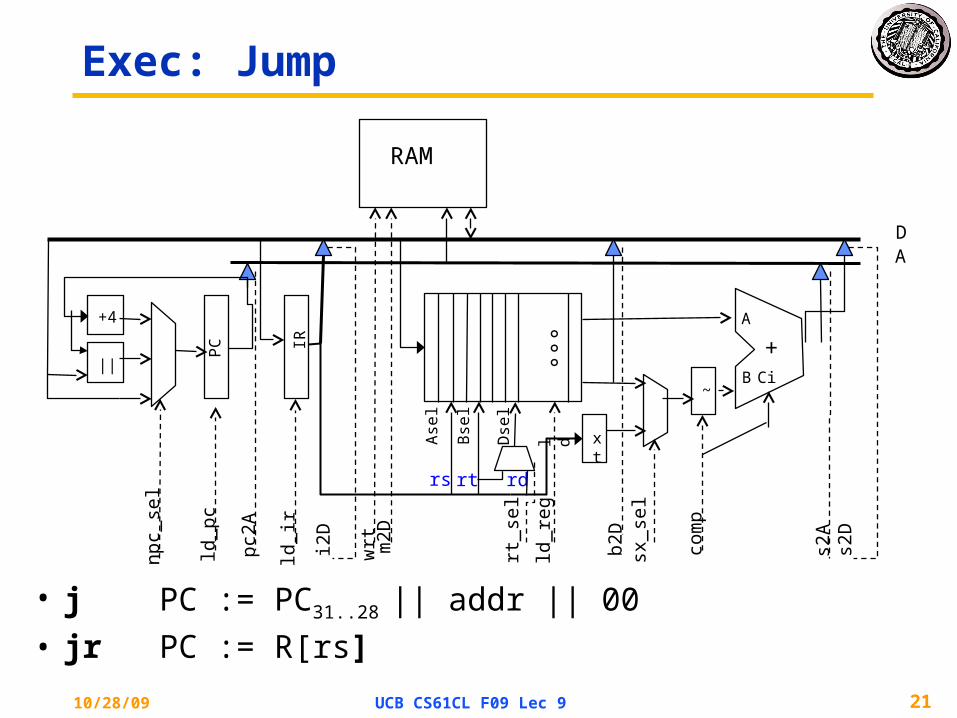
Exec: Jump
• j PC := PC31..28 || addr || 00
• jr PC := R[rs]
10/28/09 UCB CS61CL F09 Lec 9 21
°°°
Ase
l
Bse
l
Dse
l
ld
PC +
A
B Ci~
IR
RAM
AD
xt
+4
pc2A
ld_p
c
ld_i
r
wrt
m2D
ld_r
eg
sx_s
el
com
p
s2A
s2D
rs rt rd
b2D
rt_s
el
i2D
npc_
sel
||

Exec: Branch
• BEQ PC := (R[rs] == R[rt]) ? PC + signEx(im16) : PC+4
• BLTZ PC := (R[rs] < 0) ? PC + signEx(im16) : PC+4
10/28/09 UCB CS61CL F09 Lec 9 22
°°°
Ase
l
Bse
l
Dse
l
ld
PC +
A
B Ci~
IR
RAM
AD
xt
+4
pc2A
ld_p
c
ld_i
r
wrt
m2D
ld_r
eg
sx_s
el
com
p
s2A
s2D
rs rt rd
b2D
rt_s
el
i2D
||
+
npc_
sel

Exec: Branch
• PC := (R[rs] == R[rt]) ? PC + signEx(im16) : PC+4– nPC_sel = EQ ? pcAdd : PCInc
• BLTZ PC := (R[rs] < 0) ? PC + signEx(im16) : PC+4
10/28/09 UCB CS61CL F09 Lec 9 23
°°°
Ase
l
Bse
l
Dse
l
ld
PC +
A
B Ci~
IR
RAM
AD
xt
+4
pc2A
ld_p
c
ld_i
r
wrt
m2D
ld_r
eg
sx_s
el
com
p
s2A
s2D
rs rt rd
b2D
rt_s
el
i2D
||
+
npc_
sel

DataPath + Control
10/28/09 UCB CS61CL F09 Lec 9 24
°°°
Ase
l
Bse
l
Dse
l
ld
PC +
A
B Ci~
IR
RAM
AD
xt
+4
pc2A
ld_p
c
ld_i
r
wrt
m2D
ld_r
eg
sx_s
el
com
p
s2A
s2D
rs rt rd
b2D
rt_s
el
i2D
||
+
npc_
sel

25
Levels of Design Representation
Transfer Function
Transistor Physics
Devices
Gates
Circuits
FlipFlops
EE 40
HDL
Machine Organization
Instruction Set Arch
Pgm Language
Asm / Machine LangCS 61C