10/13/2005comp 120 fall 20051 13 october questions? today control
Post on 19-Dec-2015
220 views
TRANSCRIPT

10/13/2005 Comp 120 Fall 2005 1
13 October
• Questions?• Today Control

10/13/2005 Comp 120 Fall 2005 2
Synchronous Systems
LatchCombinational
logicLatch
leading
edge
trailing
edge
On the leading edge of the clock, the input of a latch is transferred to the output and held.
We must be sure the combinational logic has settled before the next leading clock edge.
Clock
data
10/13/2005 Comp 120 Fall 2005 3
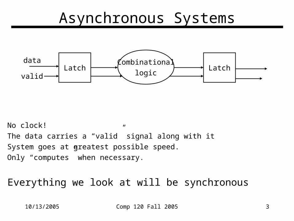
Asynchronous Systems
LatchCombinational
logicLatch
data
valid
No clock!
The data carries a “valid” signal along with it
System goes at greatest possible speed.
Only “computes” when necessary.
Everything we look at will be synchronous

10/13/2005 Comp 120 Fall 2005 4
Fetching Sequential Instructions
P
C
4
Read Address
Instruction
Instruction
Memory
How about branch?

10/13/2005 Comp 120 Fall 2005 5
Datapath for R-type Instructions
Read Reg. 15
5
5
32
Read Reg. 2
Write Reg.
Write Data
data 1
data 2
3
ALU Operation
Inst Bits 25-21
Inst Bits 20-16
Inst Bits 15-11
RegWrite
32
32

10/13/2005 Comp 120 Fall 2005 6
Fun with MUXes
Select 0
In 3
In 2
Select 0
In 1
In 0
Select 1
Out
Remember the MUX?
This will route 1 of 4different 1 bit valuesto the output.
10/13/2005 Comp 120 Fall 2005 7
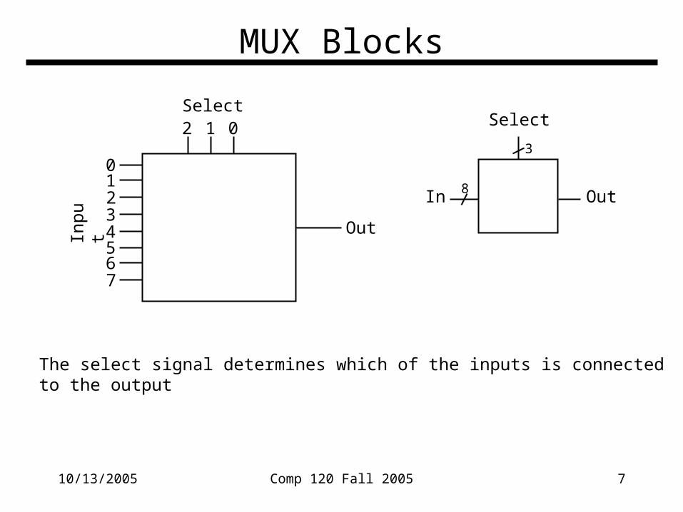
MUX Blocks
01234567
Out
2 1 0Select
Inp
ut
8
3
Select
In Out
The select signal determines which of the inputs is connectedto the output

10/13/2005 Comp 120 Fall 2005 8
Inside there is a 32 way MUX per bit
Register 0
Register 1
Register 2
Register 3
Register 4
Register ...
Register 30
Register 31
32 to1 MUX
Read Reg 1
Data 1
For EACH bit in the 32 bit register
LOT’S OF CONNECTIONS!
And this is just one port!

10/13/2005 Comp 120 Fall 2005 9
Our Register File has 3 ports
Read Reg. 15
5
5
32
Read Reg. 2
Write Reg.
Write Data
data 1
data 2
Inst Bits 25-21
Inst Bits 20-16
Inst Bits 15-11
RegWrite
32
32
2 Read Ports
1 Write Port
REALLY LOTS OF CONNECTIONS!
This is one reason we have only a small number of registers
What’s another reason?

10/13/2005 Comp 120 Fall 2005 10
Implementing Logical Functions
Suppose we want to map M input bits to N output bits
For example, we need to take the OPCODE field from the instruction and determine what OPERATION to send to the ALU.
3
ALU Operation
32
32
Map to ALU op
OPCODE bitsfrom instruction

10/13/2005 Comp 120 Fall 2005 11
We can get 1 bit out with a MUX
01234567
Out
2 1 0Select
Inp
ut
Put the INPUT HERE
Wire these to HIGH or LOW depending on the value you want OUT for that INPUT
For example, 3 input AND has INPUT7 wired HIGH and all the others wired LOW.

10/13/2005 Comp 120 Fall 2005 12
Or use a ROM
Read-Only MemoryM-bit Address N-bit Result

10/13/2005 Comp 120 Fall 2005 13
Or use a PLA
AND ArrayM-bit Input
OR ArrayN-bit OutputProduct Terms
Think of the SUM of PRODUCTS form.
The AND Array generates the products of various input bits
The OR Array combines the products into various outputs
Programmable Logic Array

10/13/2005 Comp 120 Fall 2005 14
Finite State Machines
•A set of STATES
•A set of INPUTS
•A set of OUTPUTS
•A function to map the STATE and the INPUT into the next STATE and an OUTPUT
Remember “Shoots and Ladders”?

10/13/2005 Comp 120 Fall 2005 15
Traffic Light Controller
G E/W
R N/S
Y E/W
R N/S
R E/W
G N/S
R E/W
Y N/S
10/13/2005 Comp 120 Fall 2005 16
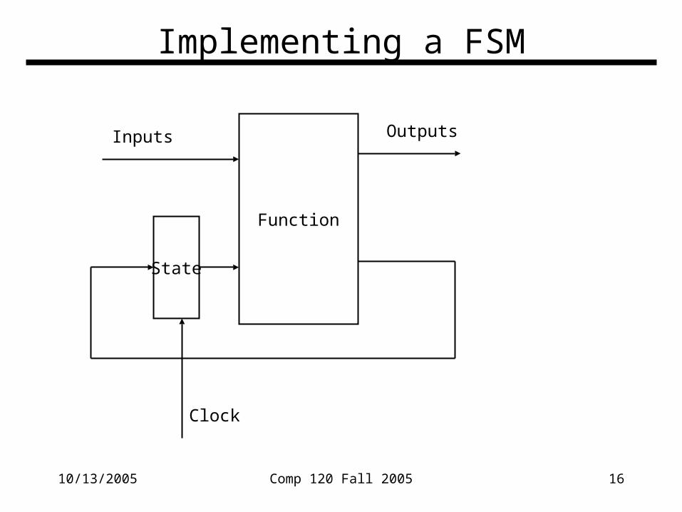
Implementing a FSM
State
Function
Inputs Outputs
Clock

10/13/2005 Comp 120 Fall 2005 17
Recognizing Numbers
Recognize the regular expression for floating point numbers
[ \t]* [-+]?[0-9]*(. [0-9]*)? (e[-+]?[0–9]+)?
Examples:
+123.456e23
.456
1.5e-10
-123
“a” matches itself
“[abc]” matches one of a, b, or c
“[a-z]” matches one of a, b, c, d, ..., x, y, or z
“0*” matches zero or more 0’s (“”, “0”, “00”, “0000”)
“Z?” matches zero or 1 Z’s

10/13/2005 Comp 120 Fall 2005 18
FSM Diagram
start
‘ ’
sign
‘+’ ‘-’
whole
‘0’ – ‘9’‘0’ – ‘9’
frac
‘.’
‘.’‘.’ ‘0’ – ‘9’
exp
‘e’
‘e’
‘0’ – ‘9’
done‘ ’
‘ ’
‘ ’

10/13/2005 Comp 120 Fall 2005 19
FSM Table
IN : STATE NEW STATE
‘ ’ : start start
‘0’ | ‘1’ | ... | ‘9’ : start whole
‘+’ | ‘-’ : start sign
‘.’ : start frac
‘0’ | ‘1’ | ... | ‘9’ : sign whole
‘.’ : sign frac
‘0’ | ‘1’ | ... | ‘9’ : whole whole
‘.’ : whole frac
‘ ’ : whole done
‘e’ : whole exp
‘e’ : frac exp
‘0’ | ‘1’ | ... | ‘9’ : frac frac
‘ ’ : frac done
‘0’ | ‘1’ | ... | ‘9’ : exp exp
‘ ’ : exp done
STATE ASSIGNMENTS
start = 0 = 000
sign = 1 = 001
whole = 2 = 010
frac = 3 = 011
exp = 4 = 100
done = 5 = 101
error = 6 = 110

10/13/2005 Comp 120 Fall 2005 20
FSM Implementation
ROM or PLA
state3
8char in
error
ok
3
Our PLA has:
•11 inputs
•5 outputs

10/13/2005 Comp 120 Fall 2005 21
FSM Take Home
• With JUST a register and some logic, we can implement complicated sequential functions like recognizing a FP number.
• This is useful in its own right for compilers, input routines, etc.
• The reason we’re looking at it here is to see how designers implement the complicated sequences of events required to implement instructions
• Think of the OP-CODE as playing the role of the input character in the recognizer. The character AND the state determine the next state (and action).

10/13/2005 Comp 120 Fall 2005 22
Highlights
• The fair starts tomorrow!