1 ece243 storage. 2 a storage mechanism can be two of: –fast –large –cheap ie., any given...
TRANSCRIPT

1
ECE243
Storage

2
Storage • A storage mechanism can be two of:
– fast– large– cheap
• ie., any given storage mechanism is either:– slow, small, or expensive
• Examples:– fast/small/cheap:– slow/large/cheap:– fast/large/expensive:

3
Storage Topics• Cache Design
• Memory Design
• Virtual Memory
• Disks

4
ECE243
Caches

5
CACHE • a small, fast storage mechanism
• contains a subset of main memory– which subset?
• there can be several “levels” of cache– may modern desktops have 3 levels (L1,L2,L3)
• caches are “invisible” to ISAs– therefore they are invisible to programs too– you know they are there– but you do not directly manage them (mostly)

6
TYPICAL MEMORY HIERARCHY
Larger, Slower, Cheaper
CPU
regs
L1 cache
memory
disk
(DRAM)(SRAM)
L2 cache
(SRAM)
Processor chip
motherboard
• L1= level 1, L2 = level 2• main memory (DRAM)
– can be ~1000X larger than an SRAM cache
• DRAM can be ~10X slower than SRAM• disk can be ~100,000X slower than DRAM

7
MEMORY METRICS• latency:
– how long it takes from request to response• ie, READ location 0xabcd
– measured in hundreds of CPU cycles• or in tens of nanoseconds
• bandwidth:– data transfer rate (bits per second)– impacted by width and speed of buses– eg: DDR SDRAM can do 2.1GB/s
• data bus: 133MHz, 64 bits wide

8
WHY CACHES? LOCALITY• tendency: programs tend to reuse data and
instructions near those they have used recently
• temporal locality: (reuse)– recently-referenced items are likely to be
referenced again soon
• spatial locality: (nearby)– items with nearby addrs tend to be referenced close
together in time

9
Locality Examplefor (I=0;I<n;I++){
sum+=A[I]);
}
• What kinds of locality are in this code?

10
CACHE REALITY
• a typical processor chip – has separate L1 caches for data and insts
• why?
– has “unified” L2 cache which holds both • data and instructions (mixed together)
• we’ll focus mainly on L1 data cache in this lecture
CPU
regs
L1 data cache
memoryunified L2 cache
Processor chip
motherboard
L1 inst cache

11
CACHE TERMINOLOGY
• capacity: how much can the cache hold? (bytes)• placement: where should an item be placed?• Identification: how do we find an item in the cache?
• Cache hit: the item we want is present– Hit rate = num_hits / num_accesses
• Cache miss: the item we want is absent– Miss rate: num_misses / num_accesses
• Replacement: on a miss, we must kick an old item out – to make room for the item we are interested in
• Replacement strategy: which item should we kick out?• Write strategy: what happens on a write?
12
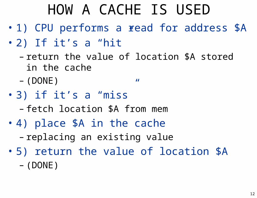
HOW A CACHE IS USED• 1) CPU performs a read for address $A
• 2) If it’s a “hit”– return the value of location $A stored in the cache – (DONE)
• 3) if it’s a “miss”– fetch location $A from mem
• 4) place $A in the cache– replacing an existing value
• 5) return the value of location $A – (DONE)

13
A 1-Byte Cache (academic only)
• holds the most recent byte accessed– pretend only byte loads and stores used
• how do you know if the cache is empty?– can’t use address==0x0---this is a valid address!– need a valid bit– V==0 means empty, V==1 means valid
• how do you know what byte is in the cache? – must store the address of the byte that is present
address Data ByteV
1-byte cache
valid bit

14
1-Byte Cache EXAMPLE
Addr Value
0x3b00 0x12
… 0x0
0x5d00 0x25
… 0x0
0x7ac0 0x56
… 0x0
0x7ace 0x78
V Addr Data
ldb r8, 0x7ace(r0)ldb r8, 0x7ace(r0)ldb r8, 0x7ac0(r0) ldb r8, 0x3b00(r0) ldb r8, 0x5d00(r0)
Mem:
Cache:
15
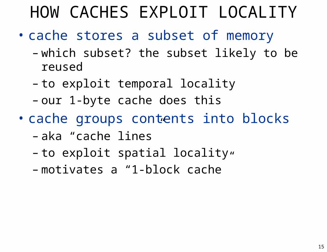
HOW CACHES EXPLOIT LOCALITY• cache stores a subset of memory
– which subset? the subset likely to be reused– to exploit temporal locality– our 1-byte cache does this
• cache groups contents into blocks – aka “cache lines”– to exploit spatial locality– motivates a “1-block cache”
16
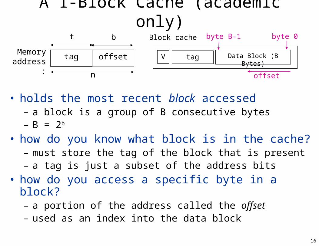
A 1-Block Cache (academic only)
• holds the most recent block accessed– a block is a group of B consecutive bytes– B = 2b
• how do you know what block is in the cache? – must store the tag of the block that is present– a tag is just a subset of the address bits
• how do you access a specific byte in a block?– a portion of the address called the offset– used as an index into the data block
tag Data Block (B Bytes)V
Block cachet b
tag offsetMemory address:
n offset
byte 0byte B-1

17
1-Block-Cache EXAMPLE • given a 16 bit addr space
• assume little-endian (like NIOS)
• assume a 1-block cache with:– t = 12 bits, b=4 bits

18
1-Block Cache EXAMPLE
Addr Value
0x3b00 0x12
… 0x0
0x5d00 0x25
… 0x0
0x7ac0 0x56
… 0x0
0x7ace 0x78
V Tag Data
ldb r8, 0x7ace(r0)ldb r8, 0x7ace(r0) ldb r8, 0x7ac0(r0)ldb r8, 0x3b00(r0)ldb r8, 0x5d00(r0)
Mem:Cache:
19
REAL CACHE IMPLEMENTATIONS
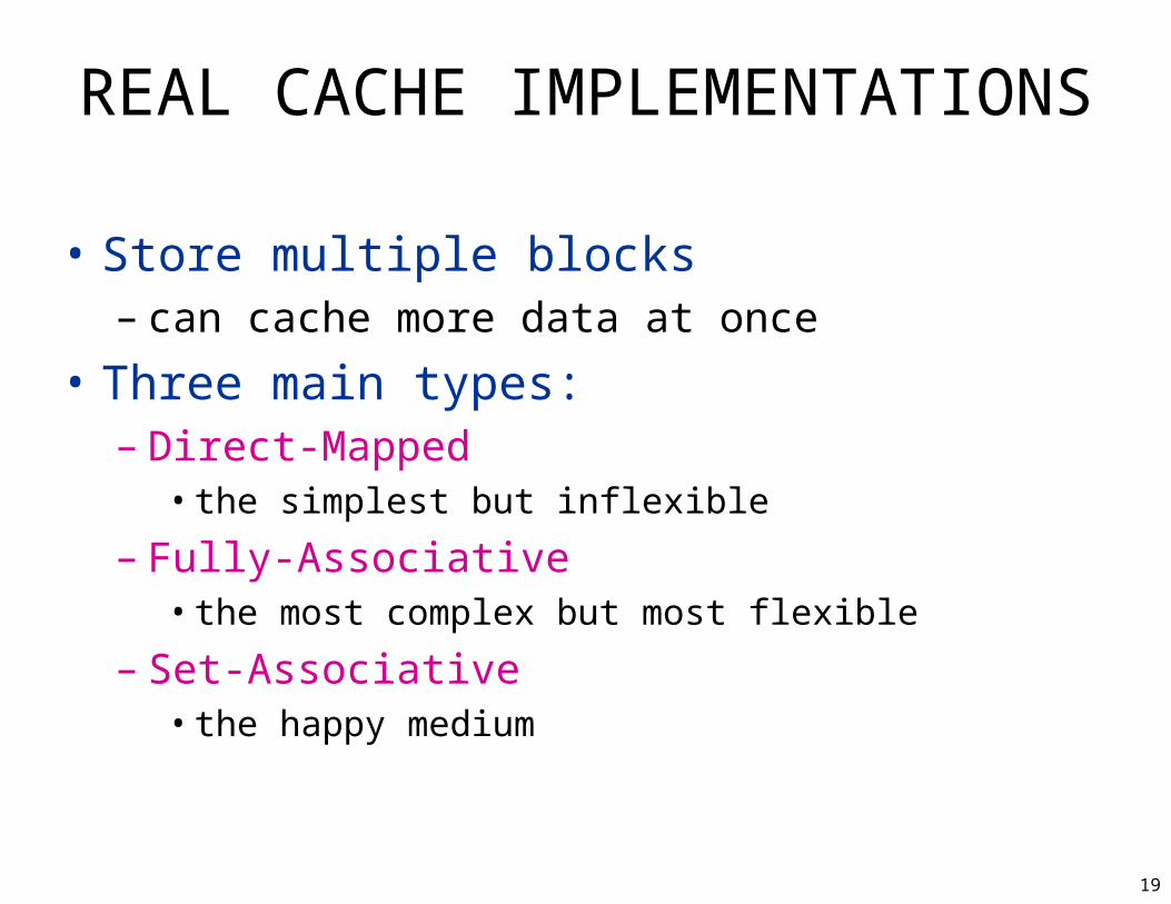
• Store multiple blocks– can cache more data at once
• Three main types:– Direct-Mapped
• the simplest but inflexible
– Fully-Associative• the most complex but most flexible
– Set-Associative• the happy medium

20
DIRECT MAPPED • each memory location maps to:
– a specific cache location
• since cache is much smaller than memory: – multiple memory blocks map to each cache block
• for a given memory address:– the set index indicates how to locate a block
• since there are multiple blocks in the cache
– the offset indicates which byte within a cache block– the tag identifies the block
• ie., which memory location does this block corresponds to?• since several memory locations map to each cache block

21
Direct-Mapped Cache
t s b
tag Set index offsetMemory address:
n
Set 0 tag Data bytes 0..B-1
tag Data Bytes 0..B-1Set S-1
Direct-mapped cache
• address space size: – 2n (bytes) (assuming byte addressable)
• block size– B = 2b (bytes)
• number of sets– S = 2s = the total number of blocks in the cache – ie, there is 1 block per set for a direct-mapped cache
• capacity:– B*S = 2 (b+s)
V
V

22
Direct-Mapped EXAMPLE • given a 16 bit addr space
• assume little-endian (like nios)
• assume a direct-mapped cache with:– t = 8 bits, s = 4 bits, b=4 bits

23
Direct-Mapped EXAMPLE
Addr Value
0x3b00 0x12
… 0x0
0x5d00 0x25
… 0x0
0x7ac0 0x56
… 0x0
0x7ace 0x78
Set V Tag Data
0
…
12
…
15
ldb r8, 0x7ace(r0)ldb r8, 0x7ace(r0)ldb r8, 0x7ac0(r0)ldb r8, 0x3b00(r0)ldb r8, 0x5d00(r0)
Mem:Cache:

24
FULLY-ASSOCIATIVE CACHE
• any block of memory can be placed in any cache block– can think of it as one large set
• good: more flexible • bad: harder to find a given cache block
– must search all of the tags!
t b
tag offsetMemory address:
n
tag Data bytes 0..B-1
tag Data Bytes 0..B-1
Set 0
V
V

25
Fully-associative example• a 16 bit addr space
• 16-byte blocks
• total capacity of 64 bytes

26
Fully-associative example
Addr Value
0x3b00 0x12
… 0x0
0x5d00 0x25
… 0x0
0x7ace 0x78
V Tag Data
ldb r8, 0x7ace(r0)ldb r8, 0x3b00(r0)ldb r8, 0x5d00(r0)
Mem:Cache:

27
SET ASSOCIATIVE
• number of “ways” within a set (W)– say “a W-way set-associative cache”
• each block of memory maps to a specific set in the cache– but can map to any block within that set
• capacity = B*S*W bytes
t s b
tag Set index offsetMemory address:
n
Set S-1
tag Data bytes 0..B-1
tag Data Bytes 0..B-1
Set 0
tag Data Bytes 0..B-1
tag Data bytes 0..B-1
V
V
V
V
28
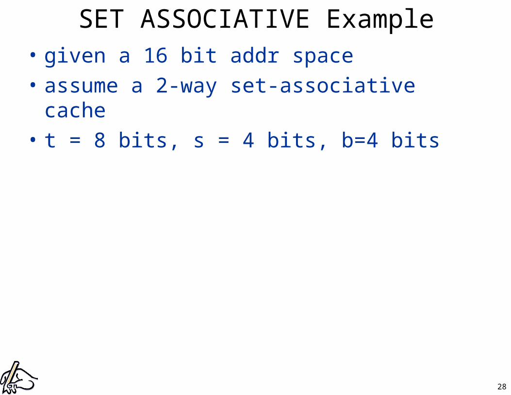
SET ASSOCIATIVE Example• given a 16 bit addr space
• assume a 2-way set-associative cache
• t = 8 bits, s = 4 bits, b=4 bits

29
SET ASSOCIATIVE ExampleSet V Tag Data
0
12
15
Addr Value
0x3b00 0x12
… 0x0
0x5d00 0x25
… 0x0
0x7ace 0x78
ldb r8, 0x7ace(r0)ldb r8, 0x3b00(r0)ldb r8, 0x5d00(r0)
Mem:
Cache:

30
Real life cache Example:• Core2:
• L1 Data Cache: – 32KB– 8-way set-associative
• L2 Cache: – 6MB– 16-way set associative
31
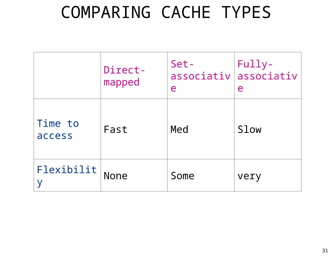
COMPARING CACHE TYPES
Direct-mapped
Set-associative
Fully-associative
Time to access
Fast Med Slow
Flexibility None Some very
32
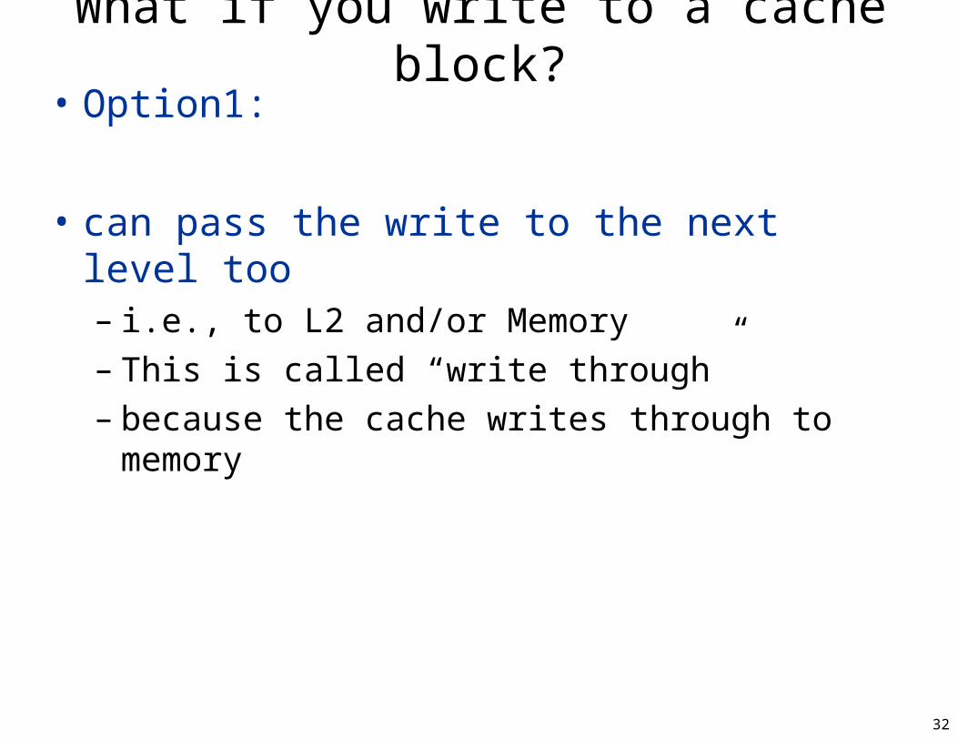
What if you write to a cache block?• Option1:
• can pass the write to the next level too – i.e., to L2 and/or Memory– This is called “write through”– because the cache writes through to memory

33
What if you write to a cache block?
tag Data bytes 0..B-1
tag Data Bytes 0..B-1
V
V
D
D
• Option2: – Don’t pass the write to the next level – only do so when the block is replaced– Need a “dirty” bit– the block has been written if the dirty bit is 1– This is called “write back”– because the cache writes the cache block back later
34
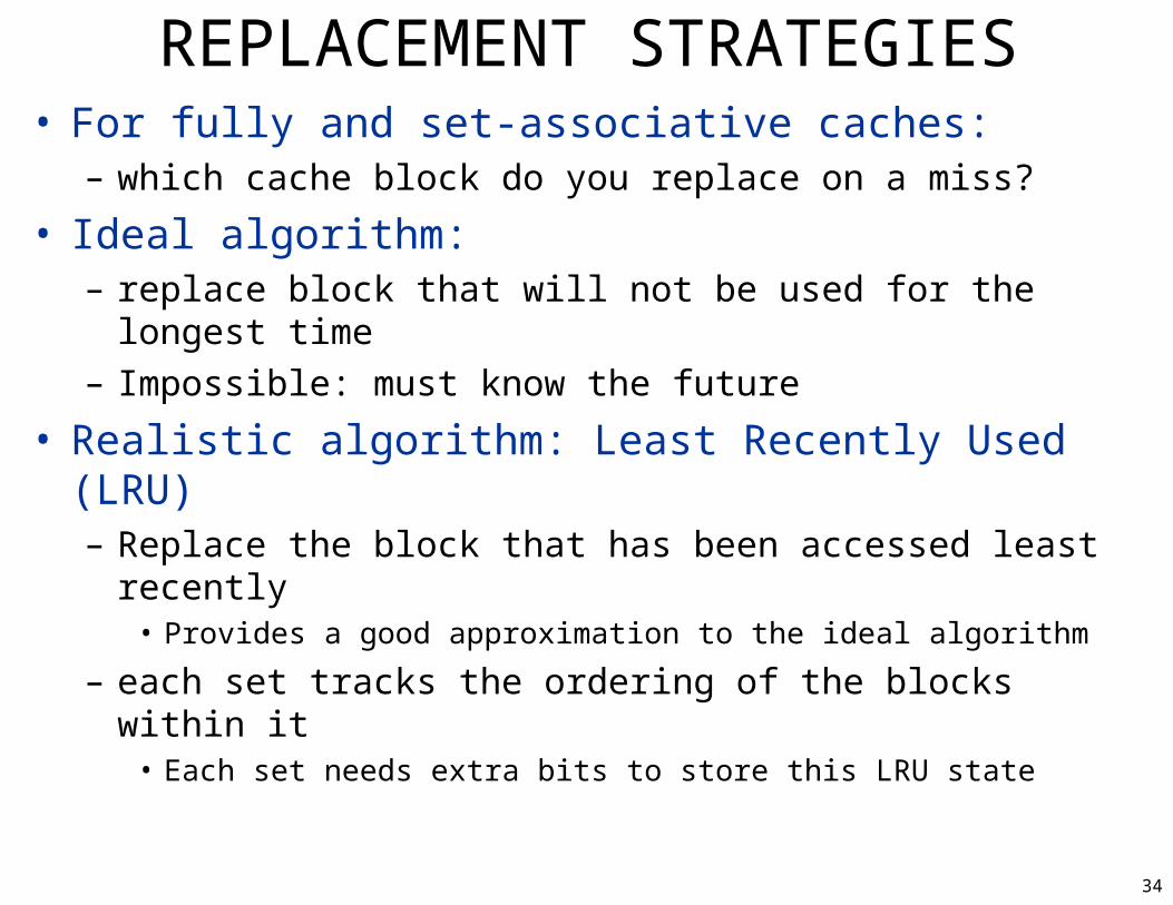
REPLACEMENT STRATEGIES• For fully and set-associative caches:
– which cache block do you replace on a miss?
• Ideal algorithm: – replace block that will not be used for the longest time– Impossible: must know the future
• Realistic algorithm: Least Recently Used (LRU)– Replace the block that has been accessed least recently
• Provides a good approximation to the ideal algorithm
– each set tracks the ordering of the blocks within it• Each set needs extra bits to store this LRU state

35
LRU IMPLEMENTATIONS
• num of bits to track LRU for 2-way set-assoc?
• for 4-way set-assoc?
• for N-way set-assoc?
tag Data bytes 0..B-1
tag Data Bytes 0..B-1
V
V
D
D
LRU
LRU

36
Other Replacement Strategies• Random:
– pick a random block – works pretty good, fast!
• Random-but-not-MRU– used in modern processors– Track MRU
• how many bits? Log2 N
– pick a random block• if you pick the MRU block then pick another block
– why is this used? • Good compromise: faster than LRU, better than pure
random

37
Total Cache Size• total_cache_size = capacity + overhead
• overhead = tags + valid_bits + dirty_bits + LRU_bits
• Ex: for 32bit addr space, how many bits for:

38
TYPES OF CACHE MISSES:• cold misses:
– the cache is empty when a program starts, all blocks are invalid
• capacity misses: – a program accesses much more data than can fit in the
cache– ex: access a 1MB array over and over, when cache is only
1KB• conflict misses:
– a program accesses two memory blocks that map to the same cache block
– these two blocks will “conflict” in the cache, causing misses– even though there is spare capacity– more likely to happen for direct-mapped caches

39
Ex: ACCESS PATTERNS • Assume:
– 1KB direct-mapped– 32B blocks– A[i] is 4B– cache is cold/empty
for (i=0;i<1024;i++){sum += A[i];
}

40
Ex: ACCESS PATTERNS • Assume:
– 1KB direct-mapped– 32B blocks– A[i] is 4B– cache is cold/empty– A[i] maps to same set as B[i]
for (i=0;i<1024;i++){sum += A[i] + B[i];
}

41
CACHE PERFORMANCE• Average_ Access_Time =
(hit_rate * hit_time) + (miss_rate * miss_penalty)
• Cache_hit_time = time for a hit – ex: 1 or 2 cycles for a hit in the L1
• Miss_penalty = time for a miss – ex: 10-20 cycles if misses L1 but hits in L2

42
Ex: Cache performance• Assume:
– a miss rate of 12.5%– a 1-cycle L1 hit latency– a 10-cycle L2 hit latency– no access misses the L2 cache.
• What is the average access time?

43
ECE243
Memory

44
RAM IMPLEMENTATION DETAILS
• a simple view of memory:
CPU MEMORYAddr bus
data bus
control

45
A NAÏVE IMPLEMENTATION
• address in, one bit out
addr
1-bit

46
A NAÏVE IMPLEMENTATION
• N copies of this circuit for N bits• All attach to the data bus via tristates
decoder
Mem cell
Addr bus
Read/!write
Data bus (in/out)
Location $0? 1 0
47
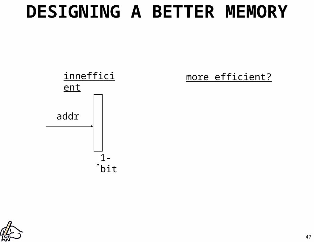
DESIGNING A BETTER MEMORY
addr
1-bit
innefficient more efficient?

48
A 1Kx1 bit memory
• 1024 bits of bit-addressable storage• most efficient as a 32 x 32 grid (square)• 10 address bits: use 5 addr bits x 5 addr bits to address the grid
32x32 memory cell array5 bit decoder
row addr (ab9-5)
Row0?
Row31?
Sense/write circuits
Data in/out (1 bit)
Column addr (ab4-0)
Control (read/write, chip select)
Addr busAb9-0
5 bits
5 bits
32 to 1 bidirectional mux
1kx1
10
addr
in/out

49
Combining Memories• Use 8 1Kx1 memories to make:
– a 1Kx8 memory (byte addressable)
1kx1 1kx1 1kx1 1kx1 1kx1 1kx1 1kx1 1kx1

50
28-PIN MEMORY CHIP • A14-0: address pins
• D7-0: data pins
• !CS: chip select: 0=enabled, 1=disabled
• !WE: write enable
• !OE: output enable,
• Vcc: power supply
• GND: ground

51
CONNECTION WITH A BUS
Addr
Data
M
A14-0
Ab14-0
Db7-0
D7-0
/15 bits
/8 bits
!CS0
• how much storage does it have?
–
52
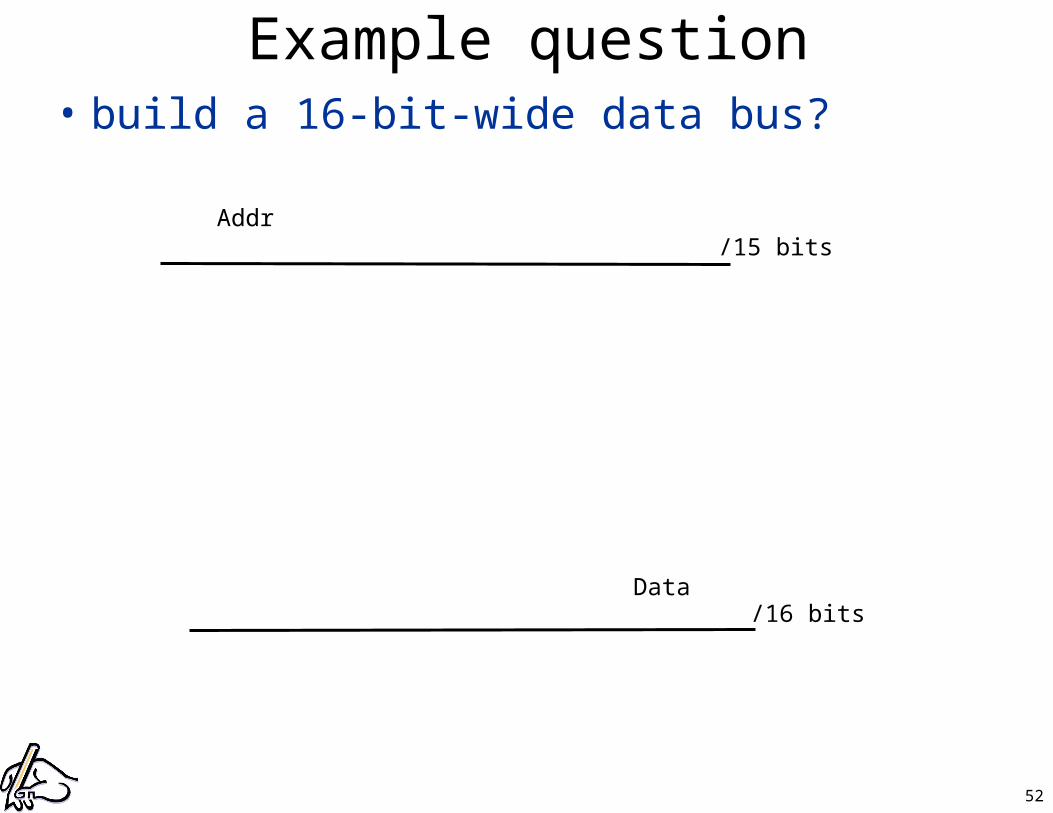
Example question• build a 16-bit-wide data bus?
Addr
Data
/15 bits
/16 bits

53
Example Question• build 64KB of storage (8-bit-wide bus)
– note: 64KB = 2^16 i.e., 16 bit addr space
Addr
Data/8 bits
/16 bits
54
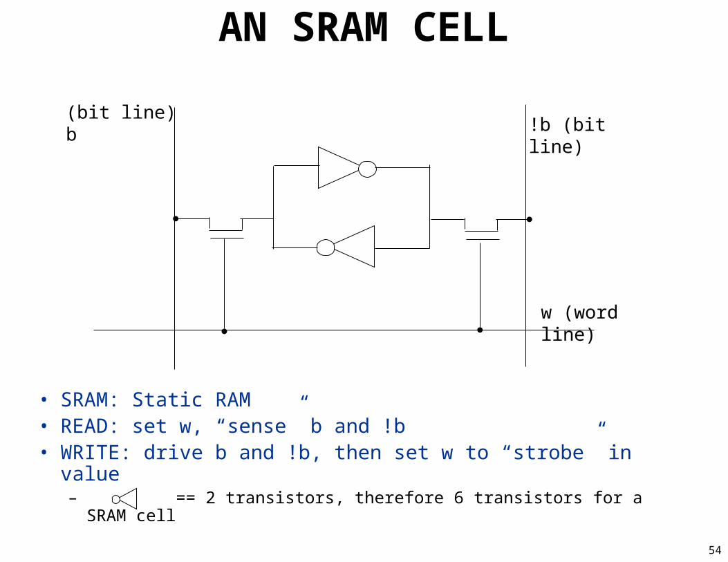
AN SRAM CELL
(bit line) b
w (word line)
!b (bit line)
• SRAM: Static RAM• READ: set w, “sense” b and !b• WRITE: drive b and !b, then set w to “strobe” in value
– == 2 transistors, therefore 6 transistors for a SRAM cell

55
SRAM CELL EXAMPLE:
(bit line) b
w (word line)
!b (bit line)
• Write a 1:

56
SRAM CELL EXAMPLE:
(bit line) b
w (word line)
!b (bit line)
• Write a 0:

57
SRAM CELL EXAMPLE:
(bit line) b
w (word line)
!b (bit line)
• Read (when cell is set to zero):
58
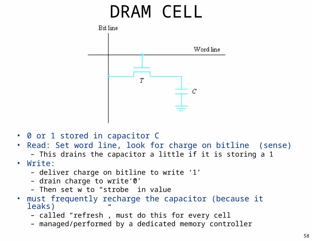
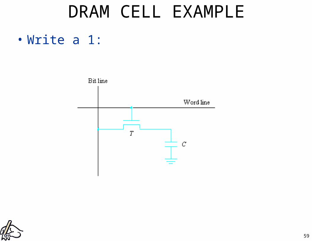
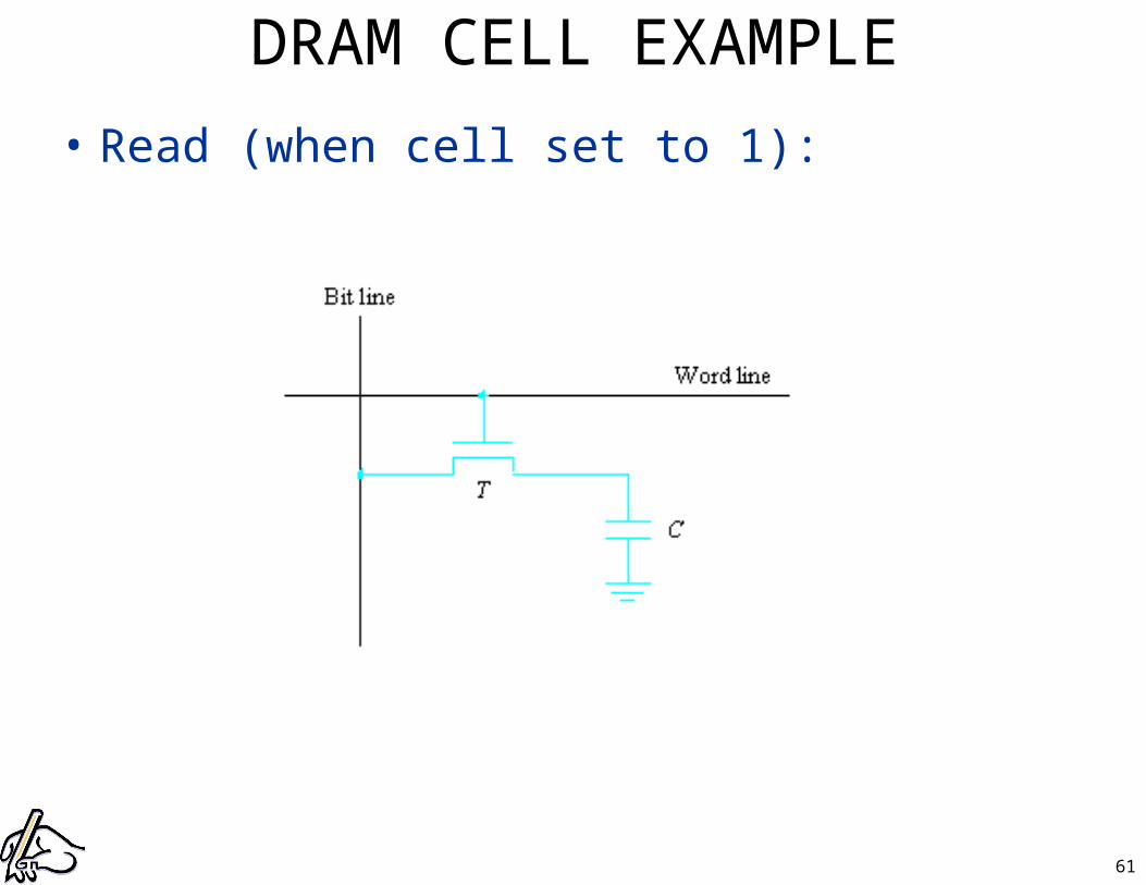
• 0 or 1 stored in capacitor C• Read: Set word line, look for charge on bitline (sense)
– This drains the capacitor a little if it is storing a 1• Write:
– deliver charge on bitline to write ‘1’– drain charge to write‘0’– Then set w to “strobe” in value
• must frequently recharge the capacitor (because it leaks)– called “refresh”, must do this for every cell– managed/performed by a dedicated memory controller
DRAM CELL
59
• Write a 1:
DRAM CELL EXAMPLE

60
• Write a 0:
DRAM CELL EXAMPLE
61
• Read (when cell set to 1):
DRAM CELL EXAMPLE
62
COMPARE SRAM TO DRAM• SRAM:
– 6 transistors---expensive– large but fast– no refresh necessary
• DRAM: – 1 transistor + 1 capacitor---cheap– small but slower– refresh necessary
63
TYPES OF DRAM• DRAM:
– dynamic RAM – asynchronous, needs to be refreshed
• SDRAM: – synchronous DRAM
• synchronized with a clock signal
– Can enter a ‘mode’ to do a “block transfer“• many bytes with one request from the CPU
• DDR-SDRAM: double-data rate SDRAM– Transfer data on both edges of the clock– rather than just the rising edge

64
DRAM REALITY1:
Need a memory controller to manage: the multiplexing of addr bits the refresh process
cpu Mem controller Memory(DRAM)
addr
R/W
request
clock
Row/col addrs
control
clock

65
DRAM REALITY2
• refresh takes time– i.e., it adds “overhead”
• typically must refresh all rows every 64ms – called the refresh period– eg: spend 2-4% of each period actually doing
refresh • 1.2-2.5ms of each 64ms period
• cannot do both reads/writes and refresh at the same time– hence memory controller tries to do refresh when
nothing else to do

66
DRAM OPTIMIZATIONS • FPM: fast-page mode
– Access entire row– rather than each row/column individually
• EDO: extended data out– Backwards compatible with FPM– Reduced wait states– optimized handshaking protocol
• BEDO: burst EDO– Pipelined, block transfers

67
connector
A ROM CELL:
• leave connected to store a 0
• disconnect to store a 1

68
TYPES OF ROM • ROM: read-only memory• PROM: programmable ROM
– one-time programmable– permanent, by “burning” fuses
• EPROM: Erasable PROM– transistors with trapped charge (instead of fuses)– can be erased by UV light
• EEPROM: electrically erasable PROM• Flash memory: similar to EEPROM
– can read a single cell, but only write blocks at a time
• PCM: phase-change memory– future replacement for flash, faster and more-dense
69
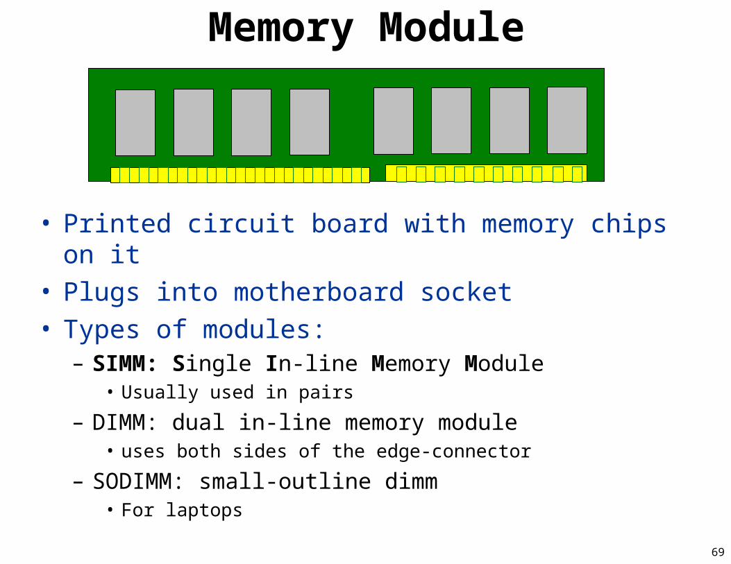
Memory Module
• Printed circuit board with memory chips on it• Plugs into motherboard socket• Types of modules:
– SIMM: Single In-line Memory Module• Usually used in pairs
– DIMM: dual in-line memory module• uses both sides of the edge-connector
– SODIMM: small-outline dimm• For laptops

70
ECE243
Virtual Memory

71
OPERATING SYSTEM (OS)• OS is just a program
– with special privileges
• implements a file system– using hard-drive– which is just another memory-mapped device
• manages devices and drivers– so you don’t have to write assembly for I/O
• allows multiple programs to share one CPU– Easy: “context switch”
• switch between one program and another• copy all p1’s registers to a struct in memory• copy all p2’s state from struct in memory to registers
– Hard: • allowing p1 and p2 to share the same memory

72
HOW CAN MULTIPLE PROGRAMS SHARE ONE MEM?
• i.e., all of your assembly programs start at memory address 0x1000000– they would all overwrite each other!
• Solution: have programs use different parts of memory– But how do you decide who is using which part
ahead of time?
• Answer: you don’t!– Have the system automatically place programs in
separate parts of memory
73
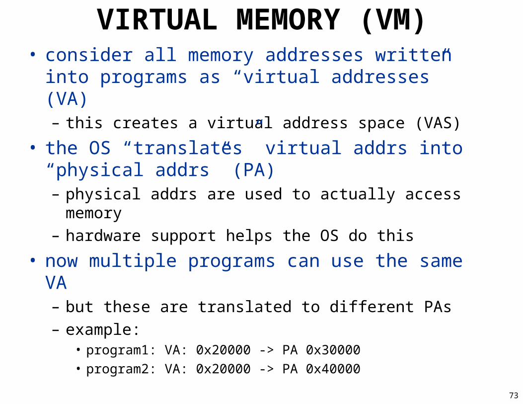
VIRTUAL MEMORY (VM)• consider all memory addresses written into programs
as “virtual addresses” (VA)– this creates a virtual address space (VAS)
• the OS “translates” virtual addrs into “physical addrs” (PA)– physical addrs are used to actually access memory– hardware support helps the OS do this
• now multiple programs can use the same VA– but these are translated to different PAs– example:
• program1: VA: 0x20000 -> PA 0x30000• program2: VA: 0x20000 -> PA 0x40000

74
THREE FEATURES OF VM1. allows multiple programs to be written using
the same virtual addrs
2. provides protection between programs– program1 cannot access the physical mem
owned by program2– if it tries, this causes a “segmentation violation” or
“segfault”
3. allows a virtual memory address space that is much larger than physical memory
– this turns memory into a cache for disk!

75
PAGES
• OS manages memory in chunks – called “pages”
• pages are normally all the same size– normally in the range of 2KB..16KB– typically 4KB for most systems
• “page fault”– when a required page is not in memory– must transfer page from disk to memory– Similar to a cache miss

76
VISUALIZING VM (4K pages)
0x0 reserved for OS
0x1000
0x2000
0x3000
0x4000
0x5000
0x6000
0x7000
Hard Drive
app2:p3
app2:p2
app2:p1
app1:p1
Physical Memory
0x1000000 app1:p1
0x1000000 app2:p1
0x1001000 app2:p2
0x1002000 app2:p3
VAS 1
VAS 2

77
VM QUESTION• Virtual Memory
– effectively turns RAM into a cache for hard drive– with page-sized “cache-blocks”
• What is the associativity of this ‘cache’?
78
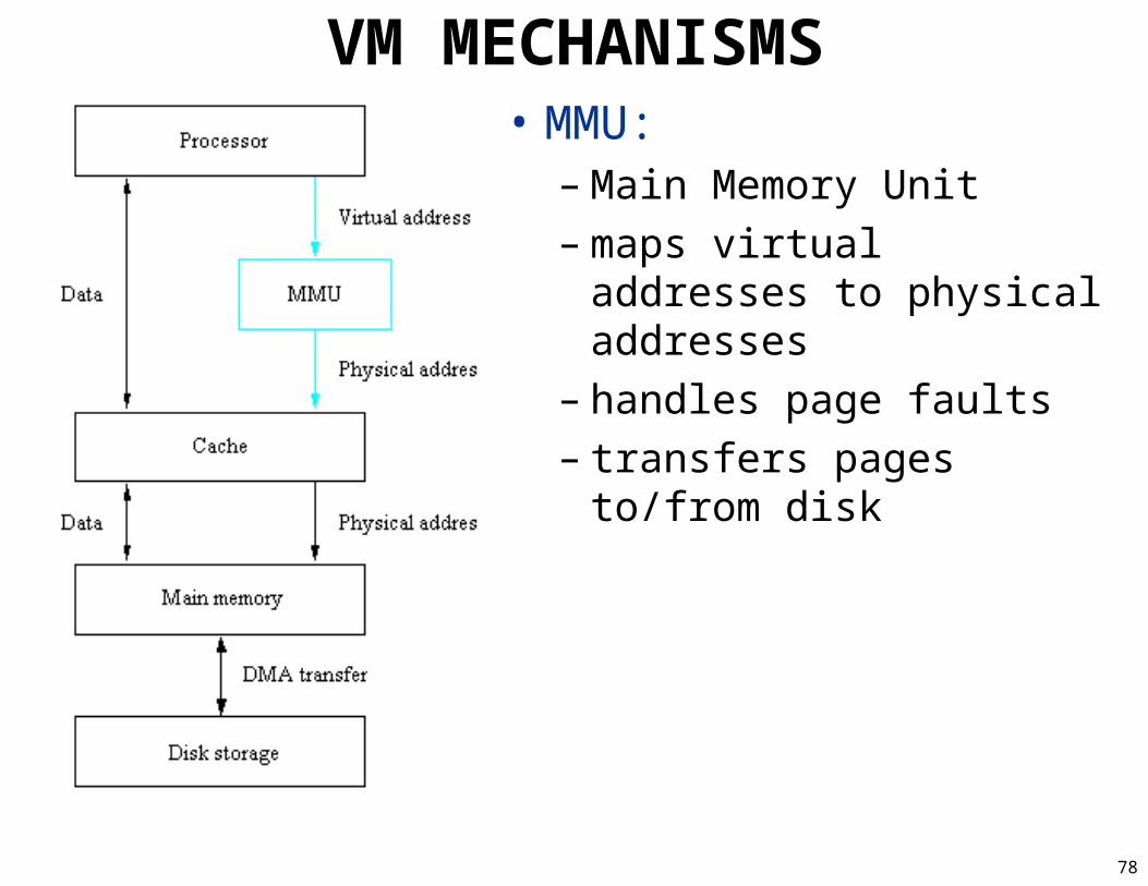
VM MECHANISMS• MMU:
– Main Memory Unit– maps virtual addresses to
physical addresses– handles page faults– transfers pages to/from disk
79
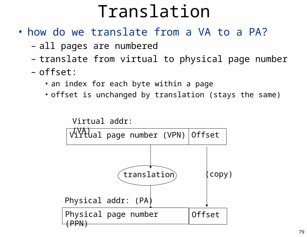
Translation• how do we translate from a VA to a PA?
– all pages are numbered– translate from virtual to physical page number– offset:
• an index for each byte within a page• offset is unchanged by translation (stays the same)
Virtual page number (VPN) Offset
(copy)translation
Virtual addr: (VA)
Physical page number (PPN) Offset
Physical addr: (PA)

80
TRANSLATION VIA PAGE TABLE• Page table:
– a table of physical page numbers (PPNs)– indexed by virtual page numbers (VPNs)– itself sits in memory
• Page table entries:– need valid bits– bits for protection (who owns the page)
• Steps for a load or store (accessing a VA):– break VA into VPN and offset– use VPN to index page table in mem, get PPN– combine PPN and offset to make PA– use PA to access memory location
• NOTE: every load or store takes two mem accesses!• What if page table entry is invalid?

81
Using a Page Table
Virtual page number (VPN) Offset
(copy)
Virtual addr: (VA)
Physical page number (PPN) Offset
Physical addr: (PA)
Use VPN to index Page table, get PPN
Use PA to index memory, perform load/store

82
PAGE TABLE EXAMPLE
0x0
0x1
0x2
0x3
…
0x1000
0x2000 app2:p1
0x3000 app1:p1
0x4000
0x5000 app2:p3
0x6000
0x7000
VA: 0x1000 000 app1:p1
VAS 1
base reg:
PageTable

83
PAGE TABLE EXAMPLE
0x0
0x1
0x2
0x3
…
0x1000
0x2000 app2:p1
0x3000 app1:p1
0x4000
0x5000 app2:p3
0x6000
0x7000
VAS 2
base reg:
PageTable
VA: 0x1000000 app2:p1
VA: 0x1001000 app2:p2
VA: 0x1002000 app2:p3
84
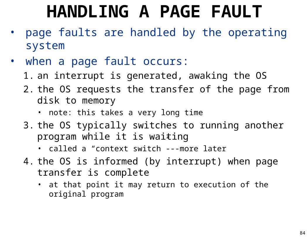
HANDLING A PAGE FAULT• page faults are handled by the operating system• when a page fault occurs:
1. an interrupt is generated, awaking the OS
2. the OS requests the transfer of the page from disk to memory• note: this takes a very long time
3. the OS typically switches to running another program while it is waiting• called a “context switch”---more later
4. the OS is informed (by interrupt) when page transfer is complete• at that point it may return to execution of the original program

85
Page Table Size• assume 4KB pages, 32-bit address space• Q1: how many page table entries are there?
• Q2: How many bits wide is a PPN?
• Q3: How many bytes for the whole page table
(excluding control bits)?

86
Translation Lookaside Buffer (TLB)• Page table is quite large
– And must be accessed for every mem reference!
• Exploit locality:– Only using a small subset of pages at any time– Keep a small cache of in-use page table entries
• TLB: – a small, fully-assoc cache of page table entries– integrated into and managed by the MMU

87
Using a TLB
Virtual page number (VPN) Offset
(copy)
Virtual addr: (VA)
Physical page number (PPN) Offset
Physical addr: (PA)
Use VPN to index Page table, get PPN
Use PA to index memory, perform load/store
Use VPN to lookup PPN in TLB
TLB hit
TLB miss

88
ECE243
Disks

89
HARD DRIVES• can store tens to hundreds of GB
• on the order of milliseconds to read– 100,000X slower than DRAM– 1,000,000X slower than SRAM

90
DISK DATA LAYOUT
• surface of the platter is divided into tracks – concentric rings
• each track is divided into sectors– consecutive bits, separated by gaps
Tracksspindle sectors
Track i
gaps

91
READING & WRITING
• the platter spins (at a rotational rate, RPM)• read/write head is attached to an arm which moves radially• read/write head magnetizes a thin film on the surface
– use two directions of magnetization to represent 0’s and 1’s– sense direction of magnetization to read
• head actually “flies” on a cushion of air– similar to flying a 747 6 feet off the ground
• in older drives, the head would “crash land” if power was cut
Read/write head
Air

92
DISK ARCHITECTURES• can have one arm with two read/write heads
– to read/write both upper and lower surfaces of platter
• can have multiple platters and arms
• Disk capacity = – #bytes/sector * avg_#_sectors/track * #tracks/surface *
#surfaces/platter * #platters/disk
• why is there an “average” number of sectors per track?
–
93
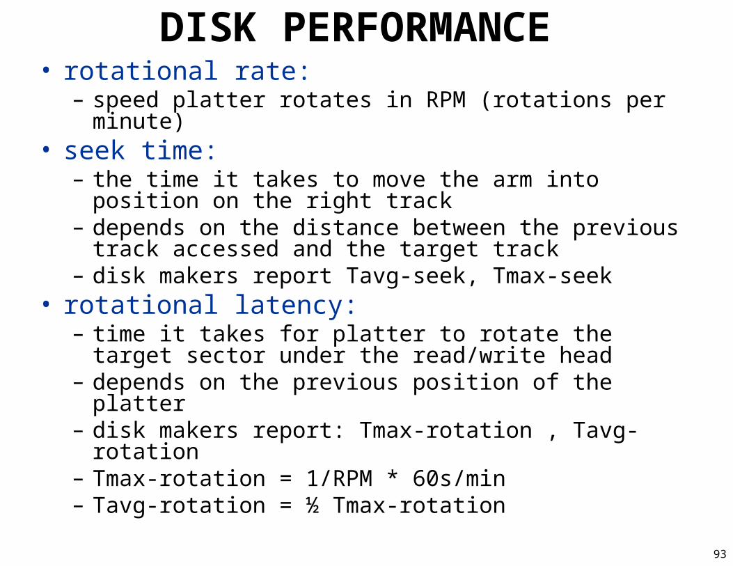
DISK PERFORMANCE • rotational rate:
– speed platter rotates in RPM (rotations per minute)• seek time:
– the time it takes to move the arm into position on the right track
– depends on the distance between the previous track accessed and the target track
– disk makers report Tavg-seek, Tmax-seek• rotational latency:
– time it takes for platter to rotate the target sector under the read/write head
– depends on the previous position of the platter– disk makers report: Tmax-rotation , Tavg-rotation– Tmax-rotation = 1/RPM * 60s/min– Tavg-rotation = ½ Tmax-rotation
94
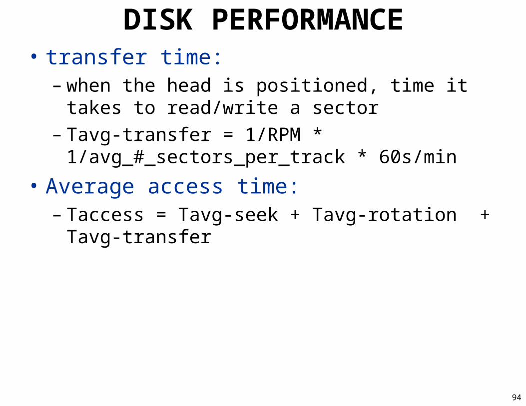
DISK PERFORMANCE• transfer time:
– when the head is positioned, time it takes to read/write a sector
– Tavg-transfer = 1/RPM * 1/avg_#_sectors_per_track * 60s/min
• Average access time: – Taccess = Tavg-seek + Tavg-rotation + Tavg-
transfer

95
EXAMPLE • Assume:
– rotational rate = 7200RPM– Tavg-seek = 9ms– average_num_sectors_per_track = 400
• compute average access time

96
DISK REALITY• to hide complexity of sectors/tracks/rotation etc:
– disk presents view of “logical blocks”– each block is the size of a sector– and numbered 0..B-1 for all B sectors on the disk
• disks must be formatted: – info added in gaps that identify sectors– mark bad sectors
• disk connected to the system bus through a “disk controller”– can transfer data in blocks between memory and disk– larger than cache blocks– called DMA “direct memory access”

97
REAL HARD DISK TYPES• ATA/EIDE: advanced technology attachment / enhanced
integrated drive electronics– IDE and ATA are the same thing, IDE is a marketing term– Can connect directly to PCI bus– Can connect directly to some Pentium motherboards– SATA: serial ATA
• SCSI: (pronounced scuzzy):– attaches to SCSI bus, can be faster than drives attached to PCI bus
• RAID: Redundant Array of Inexpensive Disks– Rather than one big expensive disk, have several inexpensive disks– Can break a single file up (called striping) into parts (called “stripes”)
• Put each stripe on a separate disk• Now can read one file faster (read many disks at once)
– Can also replicate data on the disks to improve reliability• Ie., if one disk fails, another is there as a backup

98
OPTICAL DISKS• CDs: Compact Disks
– Uses a laser to read indentations (pits) on disk– Disks may contain errors (doesn’t really matter for audio)
• CD-ROM: – like a CD, but has error checking (so can use for computer data)
• CD-R: (recordable) – can write once by using laser to burn pits
• CD-ReWritable: – can be written multiple times, similar to CD-R
• DVD: digital versatile disk: – like CD, but shorter-wavelength laser, smaller pits, more dense tracks
• DVD-R: writable DVD• DVD-RW: rewritable DVD

99
Final Note• Flash memory and similar technologies
– are quickly replacing hard drives– ex: can buy laptops with flash-like storage
• no hard drive
– saves power, size, weight
• Downside:– flash wears out (current tech)– need clever algorithms to “spread accesses”– system might tell you to replace your drive