1 dielectrics dielectrics electrically and physically separate interconnects from each other and...
TRANSCRIPT

1
Dielectrics
• Dielectrics electrically and physically separate interconnects from each other and from active regions. • Two types: - First level dielectric - Intermetal dielectric (IMD)
• First level dielectric is usually SiO2 “doped” with P or B or both (2-8 wt. %) to enhance reflow properties. • PSG: phosphosilicate glass, reflows at 950-1100˚C• BPSG: borophosphosilicate glass, reflows at 800˚C.• SEM shows BPSG oxide layer after 800˚C reflow step, showing smooth topography over step. • Undoped SiO2 often used above and below PSG or BPSG to prevent corrosion of Al .

2
Low-K Dielectrics to Decrease Capacitance of Interconnects
Requirements:• Chemical and mechanical stability• Low-K throughout all processing• Thermal stability (~500°C)• Dielectric strength
• Porosity trade off b/w low e and degradation of mechanicl, electrical, chemical properties
• Design: changes in dimensions to reduce
Capacitance
Change of line-to-line spacing
Capacitance shift:• a to b: 10070nm• c: full pores @70nm• d: Cu thickness
scaled to 2/3 of Al line of the same width &
Rs

3
Inter Level Dielectrics
BPSG used for planarization – 800°C reflow
Planarity increases with T and with %B & %P content
Reflow

4

5
Low k Dielectrics Between Metal Lines: Capacitance CIMD Dominates Delays
Problems with low k dielectrics:• Mechanical strength• Low thermal conductivity K => lower e lower K• Absorption of moisture with increasing porosity• Difficult integration with metal and masks• Dry etching and cleaning => poison via
Increased resistance – can lead to open circuit
CIMD inter-metal increases sharply with scaling
Metal barrier more efficient in Cu capping then dielectric barrier
Dielectric barrier
Nishi
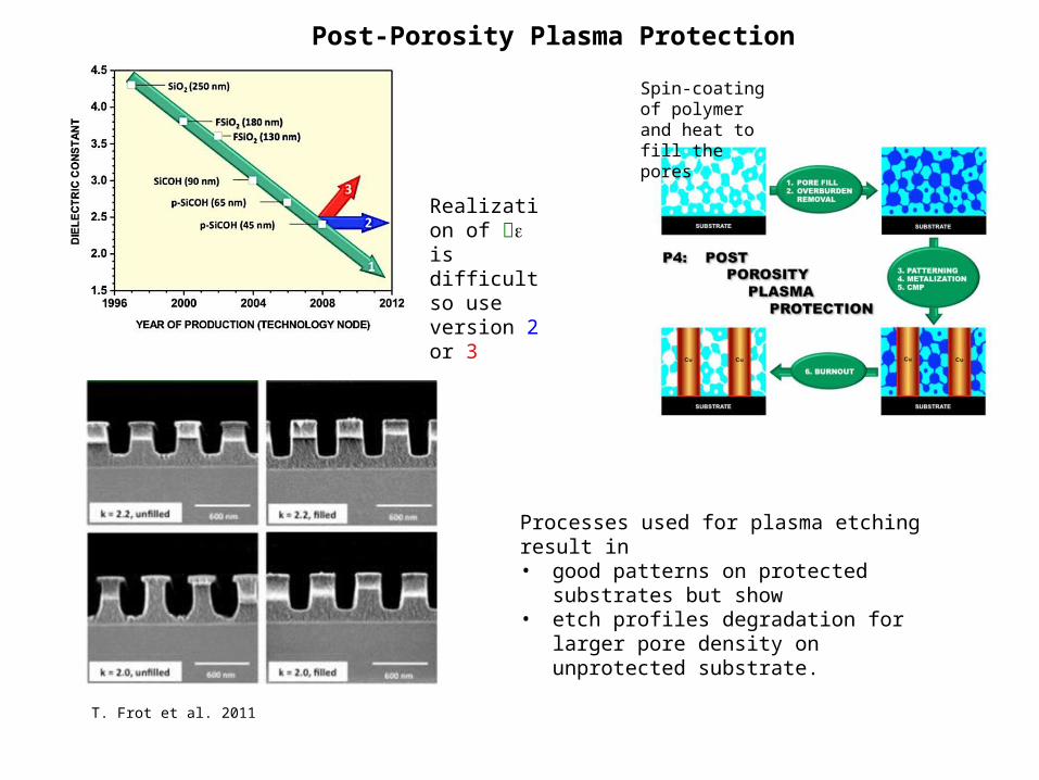
T. Frot et al. 2011
Post-Porosity Plasma Protection
Realization of e is difficult so use version 2 or 3
Spin-coating of polymer and heat to fill the pores
Processes used for plasma etching result in • good patterns on protected substrates but show • etch profiles degradation for larger pore density
on unprotected substrate.

More extreme cases of etch degradation in higher porosity materials
Porous Dielectrics

Moisture Absorption In Vias
Tsuchiya et al. 2013
In via - time b/n via etch and metallization is important
Low k dielectrics used as stopping layers can absorb moisture which degrades time dependent dielectric breakdown (TDDB ) and electromigration for Al/Cu metallization
Test of moisture resistance by SiN seen in Al pile-up at the barrier; not seen in SiCN (here Al is oxidized by the moisture at the surface). Metallization degradation.
Role of dielectric Etch Stop (ES) layers (also barrier for Cu)

9
Dielectric Layers
ESL=SiCN
Barriers for Cu needed
10
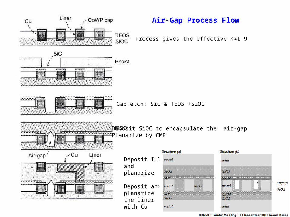
Air-Gap Process Flow
Process gives the effective K≈1.9
Gap etch: SiC & TEOS +SiOC
Deposit SiOC to encapsulate the air-gapPlanarize by CMP
Deposit ILD and planarize
Deposit and planarize the liner with Cu

11
• Intermetal dielectrics also made primarily of SiO2 today, but cannot do reflow or densification anneals on pure SiO2 because of T limitations.• Two common problems occur, cusping and voids, which can be minimized using appropriate deposition techniques.
• Planarization is required
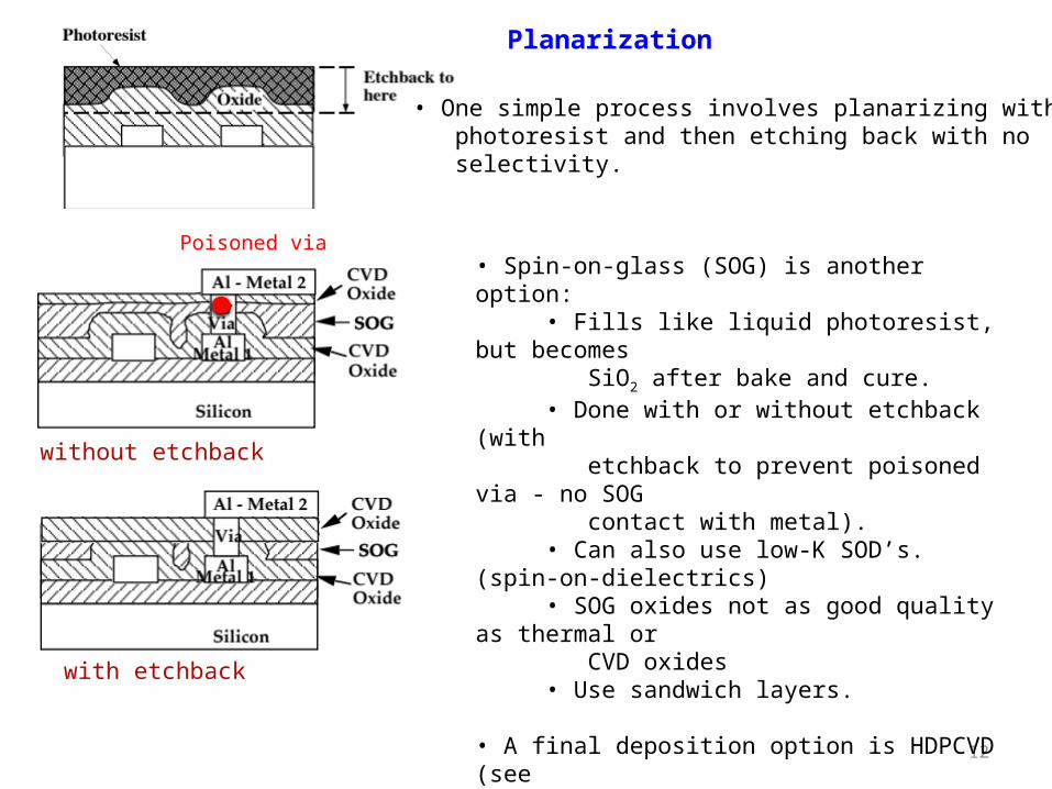
Planarization
12
• One simple process involves planarizing with photoresist and then etching back with no selectivity.
• Spin-on-glass (SOG) is another option: • Fills like liquid photoresist, but becomes SiO2 after bake and cure. • Done with or without etchback (with etchback to prevent poisoned via - no SOG contact with metal). • Can also use low-K SOD’s. (spin-on-dielectrics) • SOG oxides not as good quality as thermal or CVD oxides • Use sandwich layers.
• A final deposition option is HDPCVD (see chapter 9) which provides angle dependent sputtering during deposition which helps to planarize.with etchback
without etchback
Planarization
Poisoned via

13
• The most common solution today is CMP, which works very well.• It is capable of forming very flat surfaces as shown in the example below.
CMP

14
• The “dual damascene” process provides both the via/contact and interconnect levels simultaneously.
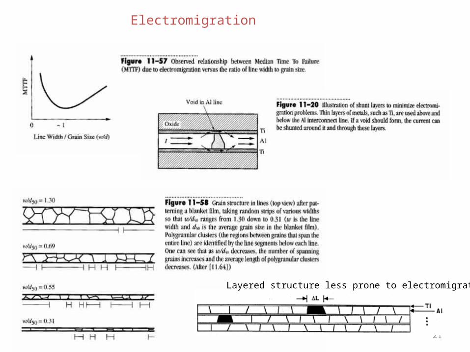
• Interconnects have also become multilayer structures.• Shunting the Al helps mitigate electromigration and can
provide mechanical strength, better adhesion and barriers in multi-level structures. •TiN on top also acts as antireflection coating for lithography.
Planarization
Planarization also help electromigration

15
Copper Deposition and CMP
Planarization in CMP affected by mechanical properties of Cu, ILD (low K) and oxide
Use reduced pressure to avoid dishing and dielectric erosion (depends also on pattern density)
Use electrochemical mechanical planarization (ECMP) – depends on applied voltage not on pressure. Advantage compared with CMP: faster and less damage to low-K ILD.
Barrier Caps:• watch for too high K• adhesion • use self-aligned selective CoWP or CoWB by electroless plating
PECVD

Defects and Faults in Interconnects
EDA360
CMP effects

17
Interconnects And Vias
• Al has historically been the dominant material for interconnects.• low resistivity• adheres well to Si and SiO2
• can reduce other oxides• can be etched and deposited easily
• Problems: • relatively low melting point and soft• need a higher melting point material for gate electrode and local interconnect polysilicon => polysides. • hillocks and voids easily formed in Al.
• Hillocks and voids form because of stress and diffusion in Al films. • Heating places Al under compression
causing hillocks. • Cooling down can places Al under
tension voids.• Adding a few % Cu stabilizes grain
boundaries and minimizes hillock formation.
18
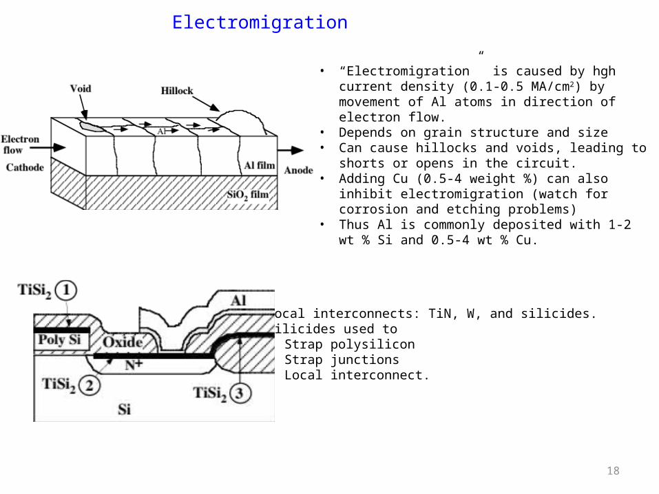
• “Electromigration” is caused by hgh current density (0.1-0.5 MA/cm2) by movement of Al atoms in direction of electron flow.
• Depends on grain structure and size• Can cause hillocks and voids, leading to shorts or opens in
the circuit. • Adding Cu (0.5-4 weight %) can also inhibit
electromigration (watch for corrosion and etching problems)• Thus Al is commonly deposited with 1-2 wt % Si and 0.5-4
wt % Cu.
• Local interconnects: TiN, W, and silicides. • Silicides used to
Strap polysiliconStrap junctionsLocal interconnect.
Electromigration

19
Rosenberg et al. 2000
Voids and Hillocks
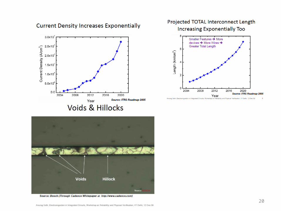
20
21
Electromigration
Layered structure less prone to electromigration

22
Electromigration
23
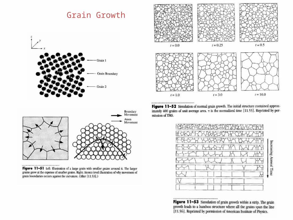
Grain Growth

24
Summary of Key Ideas
• Backend processing (interconnects and dielectrics) have taken on increased importance in recent years.
• Interconnect delays now contribute a significant component to overall circuit performance in many applications.
• Early backend structures utilized simple Al to silicon contacts.
• Reliability issues, the need for many levels of interconnect and planarization issues have led to much more complex structures today involving multilayer metals and dielectrics.
• CMP is the most common planarization technique today.
• Copper and low-K dielectrics are now found in some advanced chips and their use will likely be common in the future.
• Beyond these materials changes, interconnect options in the future include architectural (design) approaches to minimizing wire lengths, optical interconnects, electrical repeaters and RF broadcasting. All of these areas will see significant research in the next few years.