1 5. sources of errors. 5.5. fundamentals of low-noise design 5.5. fundamentals of low-noise design
TRANSCRIPT
15. SOURCES OF ERRORS. 5.5. Fundamentals of low-noise design
5.5. Fundamentals of low-noise design

2
rd
ID
edsh
rd
idsh
ID
5. SOURCES OF ERRORS. 5.5. Fundamentals of low-noise design. 5.5.1. Junction-diode noise model
4) idsh2 = 2 q ID = 2 k T / rd
3) rd k T
q ID
5) edsh2 = )2 k T / rd ) rd
2 = 2 k T rd
2) idsh2 2 q ) IF+IS ) 2 q ) ID+2IS ) 2 q ID
5.5.1. Junction-diode noise model
1) ID IS e IS IFISVD /VT
ID
At low frequencies and ID >> IS ,
idn2 = 2 q ID
Kf ID
f, Kf = 2 q ff
Note that dynamic resistances do not generate any thermal
noise since them dissipate no power, vd id = 0.
idf
idf rd
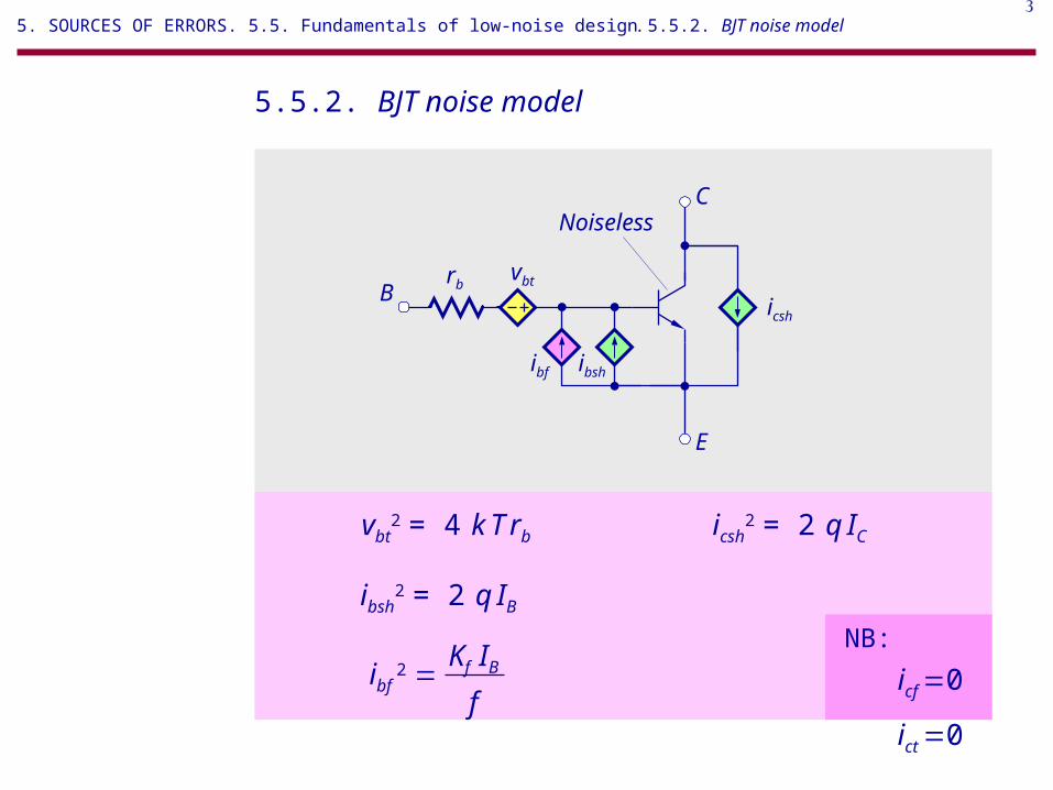
35. SOURCES OF ERRORS. 5.5. Fundamentals of low-noise design. 5.5.2. BJT noise model
5.5.2. BJT noise model
rb
icsh
B
E
CNoiseless
vbt
ibf ibsh
icsh2 = 2 q IC
ibsh2 = 2 q IB
vbt2 = 4 k T rb
ibf 2
Kf IB
f
NB: icf 0
ict 0

4
vs
RS
r
ichfe i
ro
rbB C
icsh
5. SOURCES OF ERRORS. 5.5. Fundamentals of low-noise design. 5.5.2. BJT noise model
A. Total input noise
ibf ibsh
ivbt
vn s)t) vst)t) vbt)t) ibf )t) ibsh)t)])RS rb) icsh)t)RS+rb+r
hfe
1) Total input noise vs. time, vn s)t).
2) Power spectral density of the total input noise, vn s2) f ).
vbt
vn s?

5
vs
RS
r
ichfe i
ro
C
icsh
5. SOURCES OF ERRORS. 5.5. Fundamentals of low-noise design. 5.5.2. BJT noise model
A. Total input noise
ibf ibsh
i
vn s)t) vst)t) vbt)t) ibf )t) ibsh)t)])RS rb) icsh)t)RS+rb+r
hfe
1) Total input noise vs. time, vn s)t).
2) Power spectral density of the total input noise, vn s2) f ).
vn s2 4 k T )rb RS) ibf
2 ibsh
2))RS rb)2 icsh2
RS+rb+r
hfe
2
vn s?
rbvbtvbt
vn sB

6
vn s2 4 k T )rb RS) +2 q IC
)RS rb)2
hfe
2 q IC
RS+rb+hfeVT / IC
hfe
2
vn s
5. SOURCES OF ERRORS. 5.5. Fundamentals of low-noise design. 5.5.2. BJT noise model
B. Optimum collector current
IC opt hfeVT
hfe 0.5)RS rb)
r
ichfe i
ro
rbB Civbt
vn s2 4 k T )rb RS) ibsh
2 )RS rb)2 icsh2
RS+rb+r
hfe
2
RS
ibf 0
Reference: [7]

75. SOURCES OF ERRORS. 5.5. Fundamentals of low-noise design. 5.5.2. BJT noise model
C. enin noise model
en2 vn s
2 4 k T rb ibf
2 ibsh
2) rb2 icsh
2 rb+r
hfe
2
RS= 0
in2
ibf 2 ibsh
2 vn s
2
RS2 RS=
icsh2
hfe2
vs
RS
r
ichfe i
ro
rbB Cien
in
vn s2 4 k T )rb RS) ibf
2 ibsh
2))RS rb)2 icsh2
RS+rb+r
hfe
2

85. SOURCES OF ERRORS. 5.5. Fundamentals of low-noise design. 5.5.2. BJT noise model
B
E
C
en2 4 k T rb ibf
2 ibsh
2) rb2 icsh
2 rb+r
hfe
2
in2 ibf
2 ibsh2
icsh2
hfe2
en
in
BJT enin noise model
f >> ff
rb = 100
IC = 1 mA
hfe = 100
en 1.36 nV/Hz0.5
in 1.8 pA/Hz0.5
en / in 756
RS = 756
in RS = 1.4 nV/Hz0.5

95. SOURCES OF ERRORS. 5.5. Fundamentals of low-noise design. 5.5.2. BJT noise model
D. Optimum source resistance at IC opt
vs
RS
r
ichfe i
ro
rbB Ci
Rs opt en
in IC opt
rb 2 1 + 1+hfe
en
in
IC opt

10
igsh2 = 2 q IG
idf 2
Kf ID
f
5.4.3. JFET noise model
5. SOURCES OF ERRORS. 5.5. Fundamentals of low-noise design. 5.5.3. JFET noise model
idt
G
S
D
Noiseless
igsh
idf
NB: idsh 0
idt2 = 4 k T /)3/2 gm)

11
id
5. SOURCES OF ERRORS. 5.5. Fundamentals of low-noise design. 5.5.3. JFET noise model
gmvgs
ro
G Dig
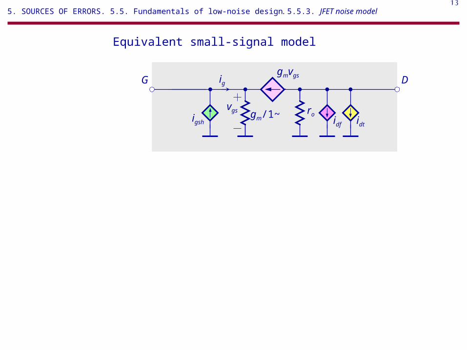
Equivalent small-signal model
igsh idtidf
vgs rgs

12
id
5. SOURCES OF ERRORS. 5.5. Fundamentals of low-noise design. 5.5.3. JFET noise model
1/gm
gmvgs
ro
G Dig
igsh idtidf
vgsvgs rgs
Equivalent small-signal model
135. SOURCES OF ERRORS. 5.5. Fundamentals of low-noise design. 5.5.3. JFET noise model
~1/gm
gmvgs
ro
G Dig
igsh idtidf
vgs
Equivalent small-signal model

145. SOURCES OF ERRORS. 5.5. Fundamentals of low-noise design. 5.5.3. JFET noise model
idvs
RS
~1/gm
gmvgs
ro
G Dig
1) Total input noise vs. time, vn s)t).
vn s?
A. Total input noise
igsh idtidf
vgs

155. SOURCES OF ERRORS. 5.5. Fundamentals of low-noise design. 5.5.3. JFET noise model
vs
RS
~1/gm
id
gmvgs
ro
G D
1) Total input noise vs. time, vn s)t).
A. Total input noise
idtidfvn s? igsh
igsh Rs
vn s)t) vst)t) + igsh)t) RS idf )t) idt)t)])1/gm)
vgs
ig

16
vn s?
5. SOURCES OF ERRORS. 5.5. Fundamentals of low-noise design. 5.5.3. JFET noise model
vs
RS
~1/gm
id
gmvgs
ro
Digsh Rs
idtidf
vn sG
A. Total input noise
1) Total input noise vs. time, vn s)t).
vn s)t) vst)t) + igsh)t) RS idf )t) idt)t)])1/gm)
2) Power spectral density of the total input noise, vn s2) f ).
vn s2 4 k T RS + igsh
2RS2
idf 2 idt
2)/gm2
vgs
ig

17
vn s?
5. SOURCES OF ERRORS. 5.5. Fundamentals of low-noise design. 5.5.3. JFET noise model
B. enin noise model
en2 vn s
2 idf
2 idt2)/gm
2
RS = 0
in2
igsh2
vn s2
RS2 RS =
vs
RS
~1/gm
id
gmvgs
ro
Digsh Rs
idtidf
vn s2 4 k T RS + igsh
2RS2
idf 2 idt
2)/gm2
vn s en
in
G
vgs
ig

185. SOURCES OF ERRORS. 5.5. Fundamentals of low-noise design. 5.5.3. JFET noise model
G
S
D
en
in
en2 idf
2 idt2)/gm
2
in2 igsh
2
JFET enin noise model
f >> ff
Vp = 2 V
IDSS = 10 mA
IG = 10 pA
en 1.8 nV/Hz0.5
in 1.8 fA/Hz0.5
en /in 1 M
RS = 1 M
in RS = 1.8 nV/Hz0.5
f >> ff
rb = 100
IC = 1 mA
hfe = 100
en 1.36 nV/Hz0.5
in 1.8 pA/Hz0.5
en / in 756
RS = 756
in RS = 1.4 nV/Hz0.5
BJT

19
idt2 = 4 k T /)3/2 gm)
idf 2
Kf ID
f
5.5.4. MOSFET noise model
5. SOURCES OF ERRORS. 5.5. Fundamentals of low-noise design. 5.5.4. MOSFET noise model
idt
G
S
D
Noiseless
idf
NB: igsh 0
idsh 0

20
id
5. SOURCES OF ERRORS. 5.5. Fundamentals of low-noise design. 5.5.4. MOSFET noise model
1/gm
gmvgs
ro
D
vn s)t) vst)t) idf )t) idt)t)])1/gm)
1) Total input noise vs. time, vn s)t).
2) Power spectral density of the total input noise, vn s2) f ).
vn s2 4 k T RS + idf
2 idt2)/gm
2
A. Total input noise
idtidfvn s?
vs
RSvn s
G
21
vn s
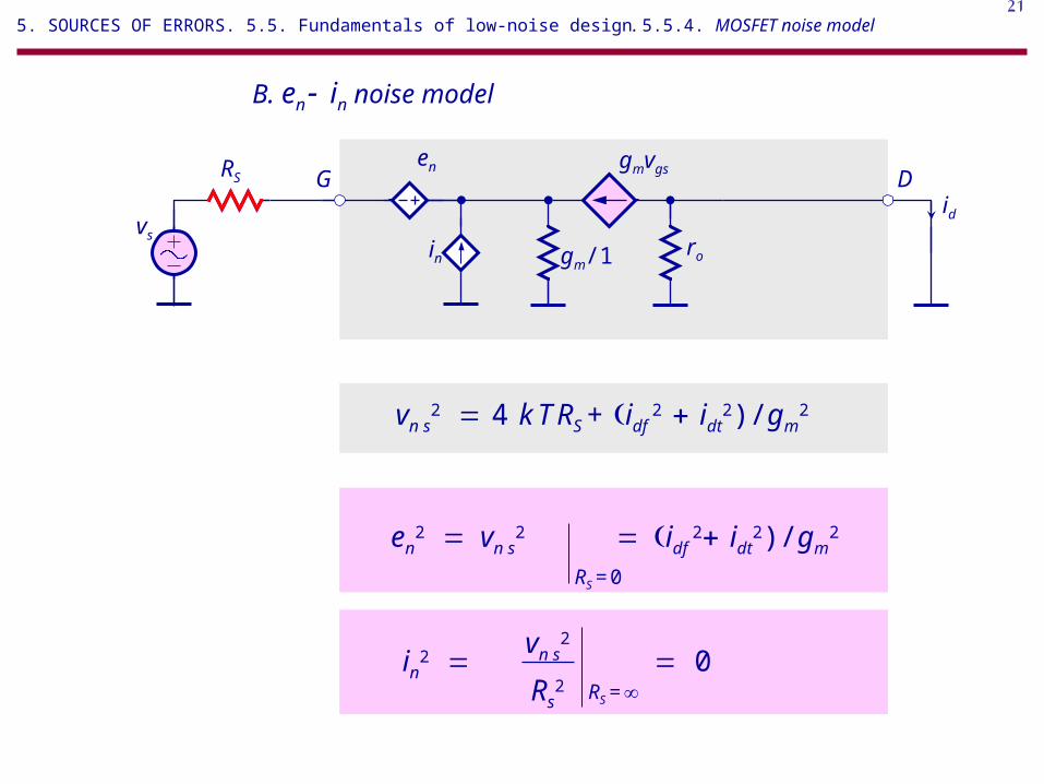
5. SOURCES OF ERRORS. 5.5. Fundamentals of low-noise design. 5.5.4. MOSFET noise model
B. enin noise model
en2 vn s
2 idf
2 idt2)/gm
2
RS = 0
in2
0vn s
2
Rs2 RS =
1/gm
id
gmvgs
ro
D
vn s2 4 k T RS + idf
2 idt2)/gm
2
vs
RSen
in
G

225. SOURCES OF ERRORS. 5.5. Fundamentals of low-noise design. 5.5.4. MOSFET noise model
G
S
D
en
en2 idf
2 idt2)/gm
2
in 0
MOSFET enin noise model
f >> ff
Vp = 2 V
IDSS = 10 mA
en 1.8 nV/Hz0.5
f >> ff
Vp = 2 V
IDSS = 10 mA
IG = 10 pA
en 1.8 nV/Hz0.5
in 1.8 fA/Hz0.5
en /in 1 M
RS = 1 M
in RS = 1.8 nV/Hz0.5
JFET

23
5.5.5. Frequency response effect
5. SOURCES OF ERRORS. 5.5. Fundamentals of low-noise design. 5.5.5. Frequency response effect
r
ichfe i
ro
rb C
icsh
ibf ibsh
i
vbtvbt
VCC iC
C
C
VBB
vs
RS
vs
RS B
The aim is to analyze the dependence of a transistor en and in
on frequency and the operating point.

24
vs
RS
Ag
1) Transconductance gain
5. SOURCES OF ERRORS. 5.5. Fundamentals of low-noise design. 5.5.5. Frequency response effect
r
ichfe i
ro
rbB C
i C
C
ic
vs
is= 1
hfe [1/j2f)C+C)]/[r+1/j2f)C+C)]
RS + rb+ rII[1/j2f)C+C)]
hfe /)RS +rb+r)
1+j2f[)RS + rb)IIr])C+C)
is
A. Total input noise

255. SOURCES OF ERRORS. 5.5. Fundamentals of low-noise design. 5.5.5. Frequency response effect
r
ichfe i
ro
rb C
icsh
ibf ibsh
i
vbtvbt
C
C
2) Power spectral density of the total input noise, vn s2) f ).
vn s2 4 k T )RS +rb) ibf
2 ibsh
2) )RS+rb)2 icsh2
RS +rb+r
hfe
2
]12f)2[
vs
RS B
vn s
hfe /)RS +rb+r)
1+j2fAg [)RS + rb)IIr])C+C)

265. SOURCES OF ERRORS. 5.5. Fundamentals of low-noise design. 5.5.5. Frequency response effect
3) en and in of the transistor.
vn s2 4 k T )RS +rb) ibf
2 ibsh
2) )RS+rb)2 icsh2
RS +rb+r
hfe
2
]12f)2[
en2 vn s
2 4 k T rb ibf
2 ibsh
2) rb2
RS = 0
in2
vn s2
RS2 RS =
icsh2
rb+r
hfe
2
]12fen)2[
ibf 2
ibsh2 ]12fin)2[
icsh2
hfe2
en)rbIIr))C+C)
inr)C+C)
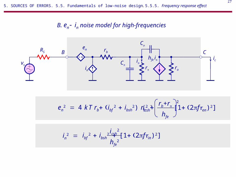
275. SOURCES OF ERRORS. 5.5. Fundamentals of low-noise design. 5.5.5. Frequency response effect
r
ichfe i
ro
rb C
i C
C
vs
RS B
en2 4 k T rb ibf
2 ibsh
2) rb2
in2
icsh2
rb+r
hfe
2
]12fen)2[
ibf 2
ibsh2 ]12fin)2[
icsh2
hfe2
en
in
B. enin noise model for high-frequencies

28
IC opt = 24 mAIC opt = 24 mA
IC = 0.1 mAIC = 0.1 mA
5. SOURCES OF ERRORS. 5.5. Fundamentals of low-noise design. 5.5.5. Frequency response effect
en) f )
nV/Hz0.5
Ag
Ag max
dB
101 103 105 108100 102 104 106 109107
-40
-20
0101 103 105 108100 102 104 106 109107
2
4
1
3
5
f, Hz
C. en) f ) for different IC
rb 100
hfe100
CpF 1
C)mA 1)pF 100
rb100
hfe100
C1 pF
C)1 mA)100 pF
en2 4 k T rb ibf
2 ibsh
2) rb2 icsh
2rb+r
hfe
2
]12fen)2[
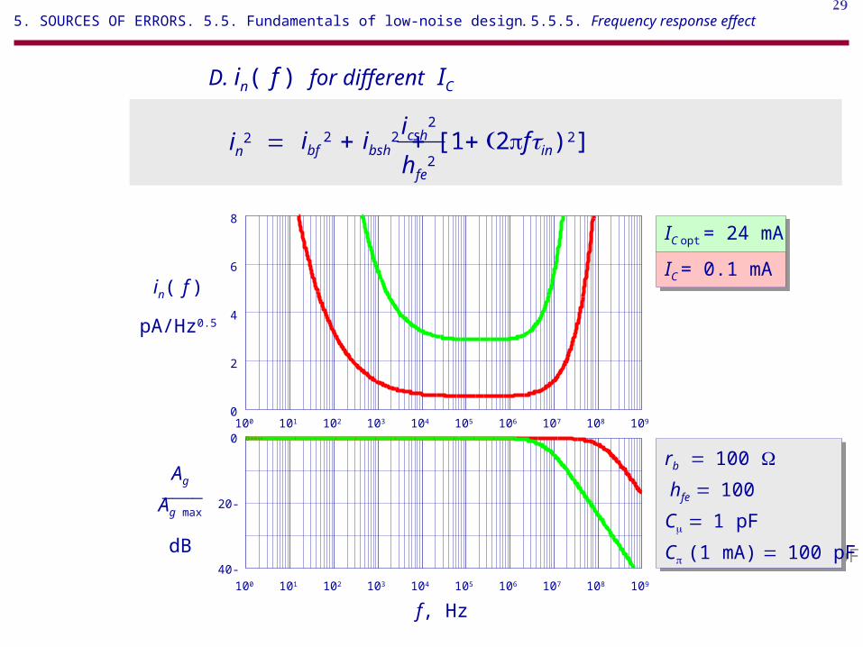
295. SOURCES OF ERRORS. 5.5. Fundamentals of low-noise design. 5.5.5. Frequency response effect
D. in) f ) for different IC
IC opt = 24 mAIC opt = 24 mA
IC = 0.1 mAIC = 0.1 mAin) f )
pA/Hz0.5
Ag
Ag max
dB
101 103 105 108100 102 104 106 109107
-40
-20
0101 103 105 108100 102 104 106 109107
2
6
0
4
8
f, Hz
rb 100
hfe100
CpF 1
C)mA 1)pF 100
rb100
hfe100
C1 pF
C)1 mA)100 pF
in2 ibf
2 ibsh
2 ]12fin)2[icsh
2
hfe2

305. SOURCES OF ERRORS. 5.5. Fundamentals of low-noise design. 5.5.5. Frequency response effect
E. Noise simulation in PSPICE
V11Vac0Vdc
V510Vdc
0
Out1
0
R2
5k
0
V20.628Vdc
R1
100
Q7
2N2222A/ZTX
Frequency
1.0Hz 10KHz 100MHz 1.0THz0
10
20
30
V(ONOISE)*1G/10V(Out1)/V(V1:+)/10V(INOISE)*1G

315. SOURCES OF ERRORS. 5.5. Fundamentals of low-noise design. 5.5.6. Comparison of the BJT, JFET and MOSFET
5.5.6. Comparison of the BJT, JFET and MOSFET
rb 40
hfe500
r o
I CmA 1
rb40
hfe500
ro
IC 1 mA
IDSS2 mA
Vp2 V
ro
ID 1 mA
vn s2 4 k T RS + igsh
2RS2
idf 2 idt
2)/gm2
vn s2 4 k T )rb RS) ibf
2 ibsh
2))RS rb)2 icsh2
RS+rb+r
hfe
2
vn s2 4 k T RS + idf
2 idt2)/gm
2

325. SOURCES OF ERRORS. 5.5. Fundamentals of low-noise design. 5.5.6. Comparison of the BJT, JFET and MOSFET
1
5
100
102 103 104 105
RS,
vn s
nV/Hz0.5
Power spectral density of
the total input noise vn s
as a function of RS
IC opt
The 1/f noise is
neglected.
The JFET gate current
is neglected.
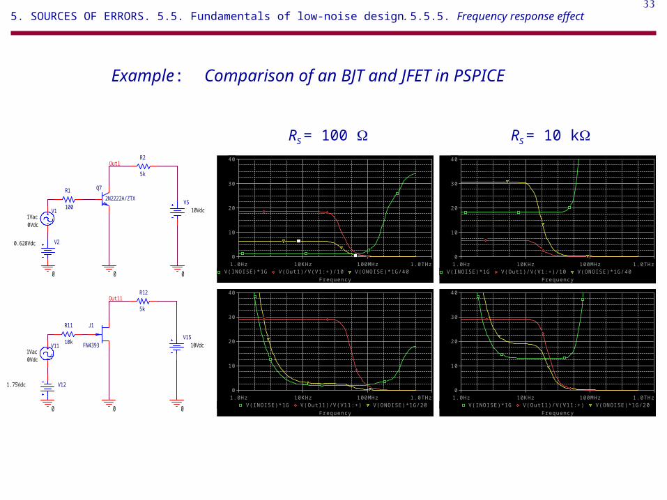
335. SOURCES OF ERRORS. 5.5. Fundamentals of low-noise design. 5.5.5. Frequency response effect
Frequency
1.0Hz 10KHz 100MHz 1.0THzV(INOISE)*1G V(Out11)/V(V11:+) V(ONOISE)*1G/20
0
10
20
30
40
Example: Comparison of an BJT and JFET in PSPICE
Frequency
1.0Hz 10KHz 100MHz 1.0THzV(INOISE)*1G V(Out1)/V(V1:+)/10 V(ONOISE)*1G/40
0
10
20
30
40
RS = 10 kRS = 100
Frequency
1.0Hz 10KHz 100MHz 1.0THzV(INOISE)*1G V(Out1)/V(V1:+)/10 V(ONOISE)*1G/40
0
10
20
30
40
V11Vac0Vdc
V510Vdc
0
Out1
0
R2
5k
0
V20.628Vdc
R1
100
Q7
2N2222A/ZTX
Frequency
1.0Hz 10KHz 100MHz 1.0THzV(INOISE)*1G V(Out11)/V(V11:+) V(ONOISE)*1G/20
0
10
20
30
40
V121.75Vdc
0
Out11
V111Vac0Vdc
R12
5k
V1510Vdc
J1
FN4393
00
R11
10k

345. SOURCES OF ERRORS. 5.5. Fundamentals of low-noise design. 5.5.6. Comparison of the BJT, JFET and MOSFET
Reference: [9]
Conclusion: Guide for selection of the preamplifier
1 10 100 1 k 10 k 100 k 1 M 10 M 100 M 1 G 10 G 100 G
MOSFET
Transformer coupling
IC amplifiers
BJT
Source resistance, RS
JFET

35
5.5.7 Noise analysis of a CE amplifier
RS
RC
RE
VCC
VBB
vs
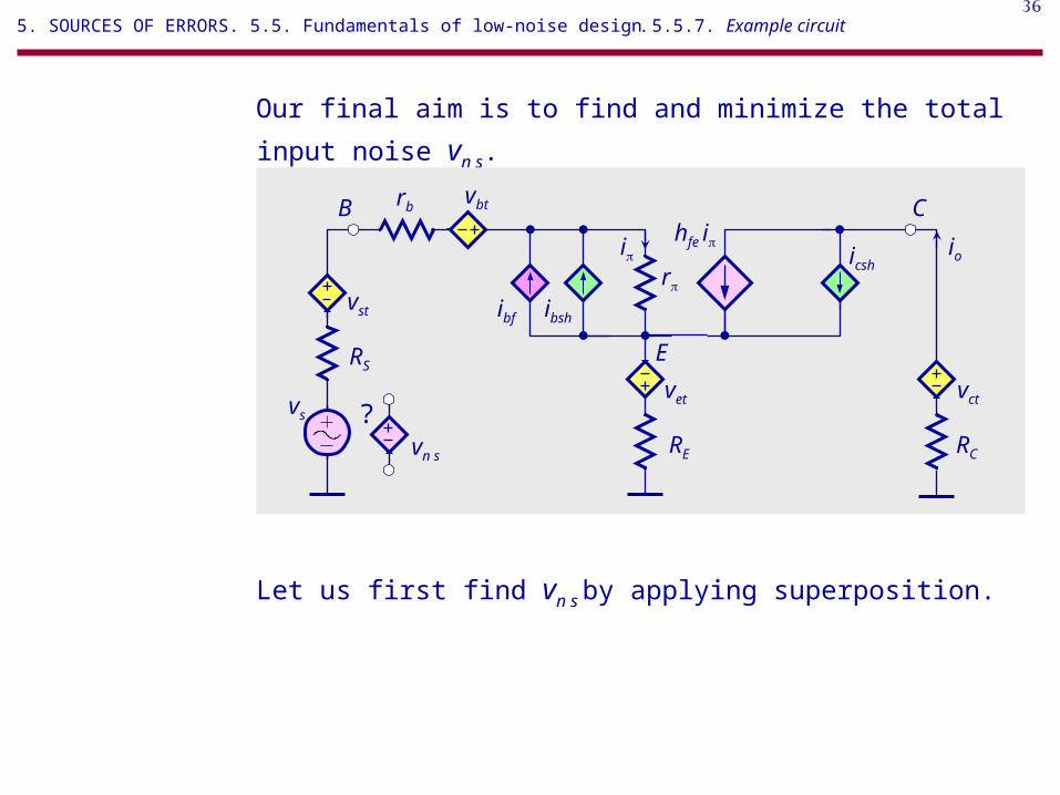
5. SOURCES OF ERRORS. 5.5. Fundamentals of low-noise design. 5.5.7. Example circuit
r
io
hfe i
ro
rb
RE RC
B
E
C
icsh
vs
RS
ibf ibsh
i
vet
vbt
vst
vct
ro
36
Our final aim is to find and minimize the total input noise vn s.
5. SOURCES OF ERRORS. 5.5. Fundamentals of low-noise design. 5.5.7. Example circuit
r
io
hfe i
rb
RE RC
B
E
C
icsh
vs
RS
ibf ibsh
i
vet
vbt
vst
vn s
?vct
Let us first find vn s by applying superposition.

37
As Gs Gs s fwd AOL
1AOL
io
vs
1) Signal gain As for vs, vst, vbt, and vet.
5. SOURCES OF ERRORS. 5.5. Fundamentals of low-noise design. 5.5.7. Example circuit
r
io
hfe i
rb
RE RC
B
E
C
vs
RS
i
As 1
RSrbrRE
hfe
1hfe RE/)RE RSrbr) 0
vet
vbt
vst

38
Abf Gibf Gbf bf fwd AOL
1AOL
io
ibf
2) Noise gain Abf for ibf and ibsh.
5. SOURCES OF ERRORS. 5.5. Fundamentals of low-noise design. 5.5.7. Example circuit
r
io
hfe i
rb
RE RC
B
E
C
vs
RS
ibf ibsh
i
Abf RSrbRE
RSrbRE r
hfe
1hfe RE/)RE RSrbr) 0

39
Acsh Gcsh Gcsh csh fwd AOL
1AOL
io
icsh
r
io
hfe i
rb
RE RC
B
E
C
icsh
vs
RS
i
3) Noise gain Acsh for icsh.
5. SOURCES OF ERRORS. 5.5. Fundamentals of low-noise design. 5.5.7. Example circuit
Acsh RE
RE RSrbr
hfe
1hfe RE/)RE RSrbr) 1

40
Act Gct Gct ct fwd AOL
1AOL
io
ict
4) Noise gain Act for icsh.
5. SOURCES OF ERRORS. 5.5. Fundamentals of low-noise design. 5.5.7. Example circuit
r
io
hfe i
RE RC
B
E
C
vs
RS
i
vct /RC
rb
Acsh 1
RC

41
5) Total input noise vs. time, vn s.
5. SOURCES OF ERRORS. 5.5. Fundamentals of low-noise design. 5.5.7. Example circuit
r
io
hfe i
RE RC
B
E
C
vs
RS
i
vn s
vn s)t) vst vbt vet
)ibf ibsh) Abf
As
icsh Acsh
As
vct Act
As
rb
vn s2) f ) 4kT RSbE+)ibf
2ibsh2) RSbE
2)RSbEr)2
hfe2
icsh2 4kT
1
RC As2
0
RSbE RS rbRE

42
r
ichfe i
RC
B Crb
vs
RS
)1+hfe) RE
E
RE
E
6) enin noise model.
en
in
in2 ibf
2 ibsh
2 icsh2
hfe2
en s2
RS2 RS =
en2 en s
2 4 k T RbE ibf
2 ibsh
2) RbE 2 icsh
2)RbE+r)2
hfe2
RS = 0
i
RbE rb RE
5. SOURCES OF ERRORS. 5.5. Fundamentals of low-noise design. 5.5.7. Example circuit

43
RSbE2
hfe
IC opt hfeVT
hfe 0.5RSbE
rb = 100
RS = 200
RE = 200
ibf 2 = 0
vbt2 = 4 k T rb
vet2 = 4 k T RE
ibsh2 = 2 q IC /
icsh2 = 2 q IC
7) Minimizing CE noise.
vn s min2 4 k T RSbE
)1 + hfe )0.5
)1 + hfe )0.51
vn s2 4 k T RSbE 2 q IC 2 q IC
RSbE+hfeVT /IC
hfe
2
102
-0.5
-0.4
-0.3
-0.2
-0.1
0
103 104
en s
norm.
dB
hfe
0.10
0.2
0.4
0.8
1.4
10 10
hfe=104
hfe=102
hfe=103
IC / IC opt
en s
norm.
dB
1.0
0.6
1.2
5. SOURCES OF ERRORS. 5.5. Fundamentals of low-noise design. 5.5.7. Example circuit
Reference: [7]

44Next lecture
Appendix: Noise analysis of the CE without applications of superposition
Reference: [7]

455. SOURCES OF ERRORS. 5.5. Fundamentals of low-noise design. Appendix: conventional noise analysis
Noise analysis of a CE amplifier
r
ichfe i
ro
rb
RE
RC
B
E
C
icsh
vn s
?
vs
RS
ibf ibsh
i
vet
vbst
RS
RC
RE
VCC
VBB
vs

46
r
iic
hfe i
ro
rb
RE
RC
B
E
C
icsh
vn s
?
vs
RS
vet
vbst
1) Disconnecting ibf and ibsh sources.
ibf ibsh
ibf ibsh
5. SOURCES OF ERRORS. 5.5. Fundamentals of low-noise design. Appendix: conventional noise analysis

47
ibf ibsh
ibf ibsh
r
iic
hfe i
ro RC
C
icsh
RE
E
rbB
vn s
vs
RS
?
vetvne = vet )ibf + ibsh) RE
1) Disconnecting ibf and ibsh sources.
vbst
5. SOURCES OF ERRORS. 5.5. Fundamentals of low-noise design. Appendix: conventional noise analysis

48
r
ichfe i
ro
rb
RE
RC
B
E
C
icsh
vet
vn s
?
vs
RS
ibf ibsh
vne = vet )ibf + ibsh) RE
1) Disconnecting ibf and ibsh sources.
i
ivbstvbst )ibf ibsh) )Rs rb)
5. SOURCES OF ERRORS. 5.5. Fundamentals of low-noise design. Appendix: conventional noise analysis

49
r
ichfe i
ro
rb
RE
RC
B Cro
icsh
vet
E
vn s
?
vs
RS
vne = vet )ibf + ibsh) RE
2) Disconnecting ibf and ibsh sources.
vbst )ibf ibsh) )Rs rb)
i
5. SOURCES OF ERRORS. 5.5. Fundamentals of low-noise design. Appendix: conventional noise analysis
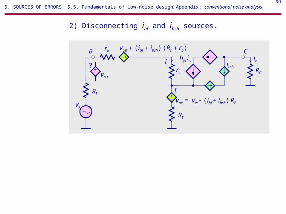
50
r
ichfe i
rb
RC
B C
RE
icsh
vet
E
vn s
?
vs
RS
vne = vet )ibf + ibsh) RE
2) Disconnecting ibf and ibsh sources.
vbst )ibf ibsh) )Rs rb)
i
5. SOURCES OF ERRORS. 5.5. Fundamentals of low-noise design. Appendix: conventional noise analysis

51
vet
r
ichfe i
rb
RC
B C
RE )1+hfe) RE
icsh
E
vn s
?
vs
RS
vne = vet )ibf + ibsh) RE
2) Disconnecting ibf and ibsh sources.
vbst )ibf ibsh) )Rs rb)
vne = vet )ibf + ibsh) RE + icsh RE
i
5. SOURCES OF ERRORS. 5.5. Fundamentals of low-noise design. Appendix: conventional noise analysis

52
r
ichfe i
rb
RC
B C
icsh
vne = vet )ibf + ibsh) RE + icsh RE
E
)1+hfe) RE
vn s
?
vn s)t) ic)t)
RS+rb+r+)1+hfe)RE
hfe
vs
RS
3) Reflecting ibf and ibsh to vn s.
vbst )ibf ibsh) )Rs rb)
vn s)t) vbst)t) vet)t) ibf )t) ibsh)t)] R* ?
i
R* RS rb RE
5. SOURCES OF ERRORS. 5.5. Fundamentals of low-noise design. Appendix: conventional noise analysis
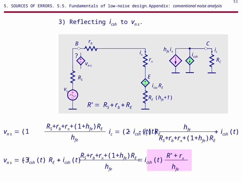
53
2) ic hfe
RS+rb+r+)1+hfe)RE
icsh )t)icsh )t) RE
r
ic
rb
RC
B C
icsh
)1+hfe) RE
icsc RE
E
vn s
?
vs
RS
hfe i
1) vn s ic)t),
RS+rb+r+)1+hfe)RE
hfe
3) vn s icsh )t) RE icsh )t)RS+rb+r+)1+hfe)RE
hfe
icsh )t)R* + r
hfe
3) Reflecting icsh to vn s.
i
R* RS rb RE
5. SOURCES OF ERRORS. 5.5. Fundamentals of low-noise design. Appendix: conventional noise analysis

54
r
ichfe i
rb
RC
B C
)1+hfe) RE
E
vn s
vs
RS
4) Total input noise vs. time, vn s)t).
i
vn s)t) vbst)t) vet)t) ibf )t) ibsh)t)] R* icsh )t)R*+ r
hfe
R* RS rb RE
5. SOURCES OF ERRORS. 5.5. Fundamentals of low-noise design. Appendix: conventional noise analysis

55
r
ichfe i
rb
RC
B C
vn s
vs
RS
vn s)t) vbst)t) vet)t) ibf )t) ibsh)t)] R* icsh )t)R*+ r
hfe
vn s2 4 k T R* ibf
2 ibsh
2) R* 2 icsh2
R*+ r
hfe
2
)1+hfe) RE
E
RE
E
5) Power spectral density of the total input noise, vn s2.
i
R* RS rb RE
5. SOURCES OF ERRORS. 5.5. Fundamentals of low-noise design. Appendix: conventional noise analysis

56Next lecture
Next lecture: