0.8v bulk-driven variable gain amplifier
DESCRIPTION
0.8V Bulk-Driven Variable Gain Amplifier. George Raikos and Spyridon Vlassis Electronics Laboratory Physics Department University of Patras http://www.ellab.physics.upatras.gr. Introduction. Utilizes : Bulk-driven transistors low-voltage operation - PowerPoint PPT PresentationTRANSCRIPT

George Raikos and Spyridon VlassisElectronics Laboratory
Physics Department
University of Patrashttp://www.ellab.physics.upatras.gr
0.8V Bulk-Driven Variable Gain Amplifier
Introduction
Utilizes :Bulk-driven transistors low-voltage
operationMaster-slave technique control voltage
gain duplicate the gain
slope
Electronics Laboratory, Physics Dept.
ICECS 2010
Based on pseudo exponential approximation function (1+x)/(1-x)≈exp(2x) linear in dB gain.
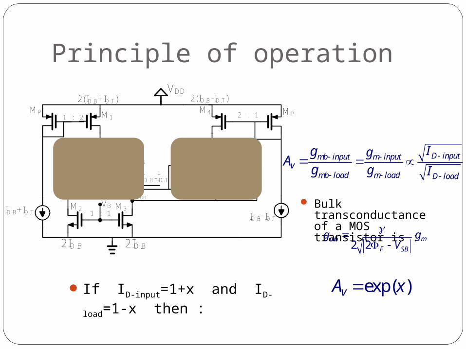
Principle of operation
VP VN
M1
M1P M1N M4P M4N
M4
M2 M3
VG VG
MP
VDD
Vop
Von
2ID.B
1 : 1
1 : 1
2(ID.B-ID.T)
1 : 1
ID.B-ID.T
ID.B-ID.T
2(ID.B+ID.T)
2ID.B
1 : 2
VBID.B+ID.T
ID.B-ID.T
2 : 1 MP
D inputmb input m input
mb load m load D loadv
Igg I
gA
g
If ID-input=1+x and ID-load=1-x then :
exp( )vA x
Bulk transconductance of a MOS transistor is :
2 2mmb
F SB
g gV

Principle of operationWe seek to make:
1m input xg
1m load xg
exp(2 )mb input
mb loadv xg
Ag
1D input xI
1D load xI
exp( )vA x

Gain Control Circuit
Generates the appropriate currents for exponential circuit controls the VGA.
Based on master-slave technique.
(k)
MC1
MC1P MC1N
MC2 MC4 MC5MC3
MC6 MC7
IT C
VDD
VG
VCM -(½)VR
IR
MS2VFb
MS1
MS1P MS1N
VG
VCM +(½)VR
Slave differ.pair
IB
ID.B+ID.T ID.B+ID.T
ID.B+ID.T
Master differ.pair
Electronics Laboratory, Physics Dept.
ICECS 2010

Gain Control Circuit
(k)
MC1
MC1P MC1N
MC2 MC4 MC5MC3
MC6 MC7
IT C
VDD
VG
VCM -(½)VR
IR
MS2VFb
MS1
MS1P MS1N
VG
VCM +(½)VR
Slave differ.pair
IB
ID.B+ID.T ID.B+ID.T
ID.B+ID.T
Master differ.pair
Electronics Laboratory, Physics Dept.
ICECS 2010
VFb the feedback voltage Thus, IR=IB+IT
IR=gmb1VR VCM :Common mode
voltage
VR relatively small (50mV)

Gain Control Circuit
The input transconductance is equal to:
(k)
MC1
MC1P MC1N
MC2 MC4 MC5MC3
MC6 MC7
IT C
VDD
VG
VCM -(½)VR
IR
MS2VFb
MS1
MS1P MS1N
VG
VCM +(½)VR
Slave differ.pair
IB
ID.B+ID.T ID.B+ID.T
ID.B+ID.T
Master differ.pair
Electronics Laboratory, Physics Dept.
ICECS 2010
The slave pair obtain equal transconductance with master pair.
gmb-
input≈(IB+IT)/VR
Linear dependence from tuning current Process independence
gmb-
input,slave≈(IB+IT)/V
R

Variable Gain Amplifier
Bulk-driven differential pair with bulk diode-connectedloads
VP VN
M1
M1P M1N M4P M4N
M4
M4R
ID.B+ID.TID.BVCM =VG
M2 M3
VS
VG VG VG
MN1 MN3MN2
MP M5
M6
Amp1
VDD
Gain Control 2
Gain Control 1
ID ID
Vop
Von
IT
IB
2ID.B
1 : 1
1 : 1
1 : 1 1 : 1
ID.B+ID.T
ID.B-ID.T
IB
2ID.B
3(ID.B-ID.T)
1 : 1
ID.B-ID.T
ID.B-ID.T
2(ID.B+ID.T)
2ID.B
1 : 1
1 : 2
Gain control circuits
Electronics Laboratory, Physics Dept.
ICECS 2010
The two gain control circuits produce the appropriate currents that bias and control the gain of the VGA.

Variable Gain Amplifier
VP VN
M1
M1P M1N M4P M4N
M4
M4R
ID.B+ID.TID.BVCM =VG
M2 M3
VS
VG VG VG
MN1 MN3MN2
MP M5
M6
Amp1
VDD
Gain Control 2
Gain Control 1
ID ID
Vop
Von
IT
IB
2ID.B
1 : 1
1 : 1
1 : 1 1 : 1
ID.B+ID.T
ID.B-ID.T
IB
2ID.B
3(ID.B-ID.T)
1 : 1
ID.B-ID.T
ID.B-ID.T
2(ID.B+ID.T)
2ID.B
1 : 1
1 : 2
Amp1 stabilize output common-mode voltage
produce the diode loads bias current
Electronics Laboratory, Physics Dept.
ICECS 2010
Thus: the gmb-input equals to (IB+IT)/VR
the gmb-loads equals to (IB-IT)/VR

Variable Gain Amplifier
VP VN
M1
M1P M1N M4P M4N
M4
M4R
ID.B+ID.TID.BVCM =VG
M2 M3
VS
VG VG VG
MN1 MN3MN2
MP M5
M6
Amp1
VDD
Gain Control 2
Gain Control 1
ID ID
Vop
Von
IT
IB
2ID.B
1 : 1
1 : 1
1 : 1 1 : 1
ID.B+ID.T
ID.B-ID.T
IB
2ID.B
3(ID.B-ID.T)
1 : 1
ID.B-ID.T
ID.B-ID.T
2(ID.B+ID.T)
2ID.B
1 : 1
1 : 2
1exp(2 )
1
T
mb input B T Bv
TB Tmb load
B
II I I
xII II
gA
g
Electronics Laboratory, Physics Dept.
ICECS 2010
Voltage gain:
where x=IT/IB
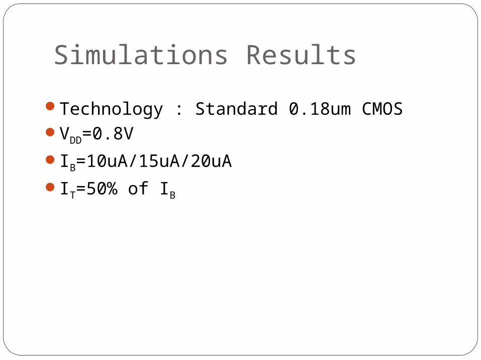
Simulations Results
Technology : Standard 0.18um CMOSVDD=0.8V
IB=10uA/15uA/20uA
IT=50% of IB

Simulations Results
Gain range of the proposed and the conventional VGA approach against tuning current IT
-5.0 5.00.0-10 10IT (μΑ)
-12.5
-10.0
-7.5
-5.0
-2.5
0.0
7.5
2.5
5.0 Introduced approach
Conventional approach
Ga
in (
dB)
-10 -5.0 0.0 5.0 10IT (μΑ)
-400
-300
-200
-100
0.0
100
200
300
400
Err
or (
mdB
)
IB=20μΑ
IB=15μΑ
IB=10μΑ
Linearity error versus tuning current IT with bias current IB as a parameter (10uA, 15uA & 20uA).
Electronics Laboratory, Physics Dept.
ICECS 2010

Simulation Results
Gain variation of VGA versus tuning variable IT with bias current IB as parameter (10uA, 15uA & 20uA)
-10 -5.0 0.0 5.0 10IT (μΑ)
Ga
in (
dB
)
-12.5
-10.0
-7.5
-5.0
-2.5
0.0
2.5
5.0
7.5
IB=10μΑ
IB=15μΑIB=20μΑ
Electronics Laboratory, Physics Dept.
ICECS 2010

Simulations Results
IB1=10uA
IB2=15uA
IB3=20uA
Comments
Technology Standard 0.18um CMOS
VDD 0.8V
IDD 267uA 395uA 530uA -
IT variation ±5uA ±7.5uA ±10uA ±50% of IB
Gain range ≈17dB ≈17dB ≈17dB -
f-3dB @gain=6.5dB 21MHz 31MHz 42MHz Pout=-25dB : Pin=-31.5dB
f-3dB @gain=-10.5dB
95MHz 143MHz 195MHz Pout=-25dB : Pin=-15.5dB
THD @gain=-10.5dB
-67dB -68dB -69dB Pout=-25dB : Pin=-15.5dB
THD @gain=-10.5dB
-44dB -45dB -46dB Pout=-15dB: Pin=-
4.5dB
ConclusionsA low-voltage VGA was introduced.Based on master-slave techniqueUtilizes bulk-driven PMOS input transistorsImplements the pseudo exponential
approximation function :exp(2 )1
1xx
x
Electronics Laboratory, Physics Dept.
ICECS 2010

Conclusions
Benefits of the proposed VGA topology : a linear-in-dB gain range almost equal to
17dBlinear gain tunability less than ±0.5dB linear errorstability over process a doubled slope of gain curve
Electronics Laboratory, Physics Dept.
ICECS 2010

Thank YouFor your Attention!!!