· volume ninety semiconductors and semimetals advances in photovoltaics: part 3 edited by gerhard...
TRANSCRIPT


VOLUME NINETY
SEMICONDUCTORS ANDSEMIMETALSAdvances in Photovoltaics: Part 3
SERIES EDITORSEICKE R. WEBERDirectorFraunhofer-Institutf€ur Solare Energiesysteme ISEVorsitzender, Fraunhofer-Allianz EnergieHeidenhofstr. 2, 79110Freiburg, Germany
CHENNUPATI JAGADISHAustralian Laureate Fellowand Distinguished ProfessorDepartment of ElectronicMaterials EngineeringResearch School of Physicsand EngineeringAustralian National UniversityCanberra, ACT 0200Australia
VOLUME NINETY
SEMICONDUCTORS ANDSEMIMETALSAdvances in Photovoltaics: Part 3
Edited by
GERHARD P. WILLEKEFraunhofer Institute for Solar Energy Systems ISE,Freiburg, Germany
EICKE R. WEBERFraunhofer Institute for Solar Energy Systems ISE,Freiburg, Germany
AMSTERDAM • BOSTON • HEIDELBERG • LONDON
NEW YORK • OXFORD • PARIS • SAN DIEGO
SAN FRANCISCO • SINGAPORE • SYDNEY • TOKYOAcademic Press is an imprint of Elsevier

Academic Press is an imprint of Elsevier
32 Jamestown Road, London NW1 7BY, UK
525 B Street, Suite 1800, San Diego, CA 92101-4495, USA
225 Wyman Street, Waltham, MA 02451, USA
The Boulevard, Langford Lane, Kidlington, Oxford OX5 1GB, UK
First edition 2014
Copyright © 2014 Elsevier Inc. All rights reserved
No part of this publication may be reproduced or transmitted in any form or by any means,
electronic or mechanical, including photocopying, recording, or any information storage and
retrieval system, without permission in writing from the publisher. Details on how to seek
permission, further information about the Publisher’s permissions policies and our
arrangements with organizations such as the Copyright Clearance Center and the Copyright
Licensing Agency, can be found at our website: www.elsevier.com/permissions.
This book and the individual contributions contained in it are protected under copyright by
the Publisher (other than as may be noted herein).
Notices
Knowledge and best practice in this field are constantly changing. As new research and
experience broaden our understanding, changes in research methods, professional practices,
or medical treatment may become necessary.
Practitioners and researchers must always rely on their own experience and knowledge in
evaluating and using any information, methods, compounds, or experiments described
herein. In using such information or methods they should be mindful of their own safety and
the safety of others, including parties for whom they have a professional responsibility.
To the fullest extent of the law, neither the Publisher nor the authors, contributors, or editors,
assume any liability for any injury and/or damage to persons or property as a matter of
products liability, negligence or otherwise, or from any use or operation of any methods,
products, instructions, or ideas contained in the material herein.
ISBN: 978-0-12-388417-6
ISSN: 0080-8784
For information on all Academic Press publications
visit our website at store.elsevier.com

CONTENTS
Contributors vii
1. State-of-the-Art Industrial Crystalline Silicon Solar Cells 1
Giso Hahn and Sebastian Joos
1. Introduction 4
2. Operation Principle of a c-Si Solar Cell 10
3. The Basic Firing Through SiNx:H Process 19
4. Recent Developments on Solar Cell Front Side 34
5. Advanced Emitter Formation 40
6. Industrial PERC-Type Solar Cells 51
7. Summary and Outlook 60
Acknowledgments 62
References 62
2. Amorphous Silicon/Crystalline Silicon Heterojunction Solar Cells 73
Christophe Ballif, Stefaan De Wolf, Antoine Descoeudres, and
Zachary C. Holman
1. Introduction 74
2. Passivating c-Si Surfaces with a-Si:H 76
3. From Passivated Wafers to Complete Solar Cells 83
4. Losses in Silicon Heterojunction Solar Cells 95
5. Industrialization and Commercialization 99
6. Future Directions and Outlook 108
Acknowledgments 110
References 110
3. Overview of Thin-Film Solar Cell Technologies 121
Bernhard Dimmler
1. Introduction 121
2. Market Shares of TF in PV 123
3. TF Device Efficiencies in Laboratory and Industry 125
4. Future Developments of TF Technologies in PV 128
References 136
Index 137
Contents of Volumes in this Series 141
v

This page intentionally left blank
CONTRIBUTORS
Christophe Ballif
Photovoltaics and Thin-Film Electronics Laboratory, Institute of Microengineering (IMT),
Ecole Polytechnique Federale de Lausanne (EPFL), Neuchatel, Switzerland. (ch2)
Stefaan De Wolf
Photovoltaics and Thin-Film Electronics Laboratory, Institute of Microengineering (IMT),
Ecole Polytechnique Federale de Lausanne (EPFL), Neuchatel, Switzerland. (ch2)
Antoine Descoeudres
Photovoltaics and Thin-Film Electronics Laboratory, Institute of Microengineering (IMT),
Ecole Polytechnique Federale de Lausanne (EPFL), Neuchatel, Switzerland. (ch2)
Bernhard Dimmler
Manz AG, Reutlingen, Germany. (ch3)
Giso Hahn
Department of Physics, University of Konstanz, Konstanz, Germany. (ch1)
Zachary C. Holman
School of Electrical, Computer, and Energy Engineering, Arizona State University, Tempe,
Arizona, USA. (ch2)
Sebastian Joos
Department of Physics, University of Konstanz, Konstanz, Germany. (ch1)
vii

This page intentionally left blank

PREFACE
The rapid transformation of our energy supply system to the efficient use of
renewable energies remains to be one of the biggest challenges of mankind
that increasingly offers exciting business opportunities as well. This truly
global-scale project is well on its way. Harvesting solar energy by photovol-
taics (PV) is considered to be a cornerstone technology for this transforma-
tion process.
This book presents the third volume in the series “Advances in
Photovoltaics” in Semiconductors and Semimetals. This series has been
designed to provide a thorough overview of the underlying physics, the
important materials aspects, the prevailing and future solar cell design issues,
production technologies, as well as energy system integration and character-
ization issues. In this volume, three distinctly different solar cell technologies
are covered in detail, ranging from state-of-the-art crystalline silicon tech-
nology, the workhorse of the booming PV market, to one of the most
advanced technologies, silicon heterojunction cells, and to an overview of
thin film solar cell technologies. Therefore, this volume represents a corner-
stone of “Advances in Photovoltaics,” as the first and the third chapter
together cover more than 98% of the current PV world market volume.
The second chapter provides a glimpse into the future of highly efficient
crystalline Si PV technologies that will allow further decrease in the cost
of PV-generated electricity available from premium modules with top per-
formance produced at prices that will become competitive with present-day
low-cost PV modules. Following the tradition of this series, all chapters are
written by world-leading experts in their respective field.
In the past 2 years, since the introduction to the first volume of this series
has been written, the world PV market has undergone a decisive transfor-
mation. Huge production overcapacity, established especially in Asia,
resulted in rapidly declining prices, often to values beyond the production
costs, when fire sales of module supplies were the only way to generate des-
perately needed cash for financially stressed companies. Subsequently, many
companies went into insolvency, followed by either restructuring under
new ownership, often from abroad, or a complete shutdown of the produc-
tion lines. The PV equipment manufacturers were especially hard hit, as they
had to survive several years practically without any new orders.
ix

Today we experience a new development: decreasing global production
capacity begins to meet further increasing PV market size, the growth of
which is fueled worldwide by the low cost of solar electricity. The conse-
quence of this process will be the further decentralization of electricity sup-
ply, as PV systems increasingly allow owners of homes and industry to
produce electricity on their own roofs and free areas, to the benefit of energy
independence and the world climate, that desperately needs rapid further
market penetration of renewables to decrease the emission of climate gases.
GERHARD P. WILLEKE AND EICKE R. WEBER
Fraunhofer ISE, Freiburg, Germany
x Preface

CHAPTER ONE
State-of-the-Art IndustrialCrystalline Silicon Solar CellsGiso Hahn1, Sebastian JoosDepartment of Physics, University of Konstanz, Konstanz, Germany1Corresponding author: e-mail address: [email protected]
Contents
1. Introduction 41.1 History 41.2 General routes for cost reduction 51.3 PV market today 71.4 Basic structure of an industrial c-Si solar cell 9
2. Operation Principle of a c-Si Solar Cell 102.1 Band diagram 102.2 Solar cell parameters 122.3 Fundamental efficiency limit of an ideal c-Si solar cell 132.4 Two-diode model 142.5 Radiative recombination 142.6 Auger recombination 152.7 SRH recombination 162.8 Surface recombination 172.9 Recombination and saturation current density 182.10 Optical losses 18
3. The Basic Firing Through SiNx:H Process 193.1 Wafer washing, texturization, and cleaning 203.2 Phosphorus diffusion 223.3 Edge isolation 253.4 SiNx:H deposition 253.5 Metallization via screen-printing 273.6 Solar cell characterization 33
4. Recent Developments on Solar Cell Front Side 344.1 Wafer sawing 344.2 Alkaline wafer texturing 354.3 Front contact metallization 35
5. Advanced Emitter Formation 405.1 Improvement of homogeneous emitters 415.2 Selective emitters 42
6. Industrial PERC-Type Solar Cells 516.1 Dielectric rear side passivation 52
Semiconductors and Semimetals, Volume 90 # 2014 Elsevier Inc.ISSN 0080-8784 All rights reserved.http://dx.doi.org/10.1016/B978-0-12-388417-6.00005-2
1
6.2 Formation of local rear contacts 546.3 Boron–oxygen related degradation 576.4 State-of-the-art industrial PERC solar cells 59
7. Summary and Outlook 60Acknowledgments 62References 62
ABBREVIATIONSA area
ALD atomic layer deposition
APCVD atmospheric pressure chemical vapor deposition
ARC antireflective coating
a-Si amorphous silicon
BSF back surface field
Bs substitutional boron concentration
cA,n (cA,p) Auger recombination coefficient for electrons (holes)
crad radiative recombination coefficient
c-Si crystalline silicon
Cz Czochralski
d layer/wafer thickness dBSFD+ diffusion constant in the BSF
DI deionized
Dn (Dp) diffusion constant of electrons (holes)
E energy
ECV electrochemical capacitance voltage
EF (EFi) (intrinsic) Fermi energy level
EFG edge-defined film-fed growth
EFn (EFp) quasi-Fermi energy level of electrons (holes)
Eg band gap energy
Ephot photon energy
EQE external quantum efficiency
Et energetic position of the trap level
EVA ethylene vinyl acetate
FCA free carrier absorption
FF fill factor
FZ float zone
h Planck’s constant
HIT heterojunction with intrinsic thin-layer
I current
IBC interdigitated back contact
IPA isopropyl alcohol
IQE internal quantum efficiency
j current density
j0 saturation current density
j01 ( j02) saturation current density of the first (second) diode
j0e saturation current density of the emitter
2 Giso Hahn and Sebastian Joos

jl light-generated current density
jsc short circuit current density
k Boltzmann’s constant
L+ diffusion length in the BSF
LFC laser fired contacts
Ln (Lp) diffusion length of electrons (holes)
LPCVD low pressure chemical vapor deposition
mono-Si monocrystalline Si
mpp maximum power point
mc-Si multicrystalline Si
n electron concentration
n+ (n++) (very) highly n-doped
n0 electron concentration in the dark
NA (ND) acceptor (donor) concentration
NA+ acceptor concentration in the BSF
nair (nSi, nSiN) refractive index of air (c-Si, SiN)
ni intrinsic carrier concentration
Nt trap density
Nts areal trap density at the surface
Oi interstitial oxygen
p hole concentration
p+ highly p-doped
p0 hole concentration in the dark
PECVD plasma-enhanced chemical vapor deposition
PERC passivated emitter and rear cell
PERL passivated emitter and rear locally diffused
PERT passivated emitter and rear totally diffused
pphot photon power density
PSG phosphor silicate glass
Psurf phosphorous surface concentration
Ptot total power loss
PV photovoltaic
q elementary charge
R recombination rate
RA Auger recombination rate
Rrad radiative recombination rate
Rs series resistance
Rs,tot total series resistance
RSRH Shockley-Read-Hall recombination rate
Rsh shunt resistance
Rsheet sheet resistance of the emitter
s (sn) (sp) surface recombination velocity (of electrons or holes)
sb surface recombination velocity at the backside
SCR space charge region
seff effective surface recombination
SIMS secondary ion mass spectrometry
SRH Shockley-Read-Hall
STC standard test conditions (1000 W/m2, AM1.5g spectrum, 25 �C)UMG upgraded metallurgical grade
3State-of-the-Art Industrial Crystalline Silicon Solar Cells

V voltage
vn (vp) thermal velocity of electrons (holes)
Voc open circuit voltage
Wp Watt peak (power of 1 W under STC)
α absorption coefficient
ΔEF splitting of quasi-Fermi levels
Δn excess charge carrier density
η conversion efficiency
Φ photon flux
λ wavelength
ρSi density of Si
ρ resistivity
σn (σp) capture cross section for electrons (holes)
τA Auger lifetime
τb bulk lifetime
τeff effective lifetime
τrad radiative lifetime
τSRH Shockley, Read, Hall lifetime
τ minority charge carrier lifetime
1. INTRODUCTION
Solar cells fabricated based on crystalline Si (c-Si) generate electricity
from sunlight by absorbing photons and generating electron–hole pairs,
which are separated by a pn-junction. The pn-junction creates an electric
field in the semiconductor and the separated charge carriers have to leave
the solar cell via electrical contacts to perform work in an external circuit.
A solar cell in operation is therefore essentially an illuminated large area
diode, where emitter and base regions are contacted by metals to extract
the carriers.
1.1. HistoryThe first c-Si solar cell operating using the principle described above was
reported in 1953 (Chapin et al., 1954), although research toward this
achievement dates back to the 1940s (e.g., Ohl, 1941; Shockley, 1950).
In the decades to follow, research was first directed toward application of
the photovoltaic (PV) effect in space (powering satellites) or for terrestrial
stand-alone systems. As for those applications the total cost of power gen-
eration was not the main issue, research was mainly driven by improving
the conversion efficiency η, which is the ratio between output power from
the PV device (generated from the solar cell or complete solar module) and
4 Giso Hahn and Sebastian Joos

input power (impinging photon flux). The oil crisis in 1973 led to consid-
erations to use PV also for terrestrial applications in larger scale as an alter-
native to fossil fuels. Since then a lot of R&D activities was focused on
reducing the cost of PV electricity generation to make it attractive for mar-
ket penetration.
In research, a lot of progress was made in improving efficiency by devel-
oping new cell designs and applying novel processing steps, leading to effi-
ciencies as high as 25% using standard test conditions (STC: 1000 W/m2
illumination, AM1.5g spectrum, 25 �C) in 1999 (Zhao et al., 1999), indi-
cating the efficiency potential of c-Si. This efficiency was reached on
extremely pure float zone (FZ) silicon and on small scale (4 cm2) without
the main part of the front side metallization grid being taken into account
for the efficiency measurement (so-called designated area measurement)
and using a very complex processing scheme. For most industrial applica-
tions, a full area measurement and cost-effective c-Si materials are of higher
interest. In addition, the number and complexity of processing steps needed
for cell fabrication has to be low, to allow a cost-efficient production. Here,
the main challenge for industrial c-Si solar cells becomes visible: there is a
trade-off between more complex processing on higher quality material all-
owing higher efficiencies, and less complex processing, e.g., in combination
with a lower c-Si material quality.
1.2. General routes for cost reductionThe lower efficiency for lower cost materials and less complex processing
might be advantageous cost-wise at cell level, but as there are also area
related cost factors at module and system level (e.g., costs for module glass
and installation), the question which route is more promising is not easy to
answer. Therefore, a lot of different technologies have been developed over
the past decades. This includes c-Si materials as well as solar cell fabrication
processes.
The Si feedstock of highest quality stems from the so-called Siemens
route using rods for Si production from the gas phase, which still accounts
for the majority of produced Si wafers for industrial solar cells, with fluidized
bed reactors as an alternative (Fabry and Hesse, 2012). So-called upgraded
metallurgical grade (UMG) Si can be produced with significantly less energy
needed per kg of fabricated Si, but a higher impurity concentration is the
consequence, with relatively high amounts of, amongst others, B and
P still present acting as doping elements in Si. This might cause problems
as after crystallization the material will be partly compensated, and due to
5State-of-the-Art Industrial Crystalline Silicon Solar Cells

different segregation coefficients of B and P their concentrations and there-
fore resistivity, influenced by the net doping, changes with ingot height
(Ceccaroli and Pizzini, 2012; Heuer, 2013).
For c-Si materials, three different material classes have been important for
PV in the past, as they have already been in industrial production in signif-
icant quantities. Monocrystalline Si (mono-Si) pulled using the Czochralski
(Cz) method shows the lowest amount of extended crystal defects (like, e.g.,
grain boundaries, dislocations, precipitates), but normally contains a high
amount of O, mainly in interstitial form (Oi) (Zulehner, 1983). Cast mul-
ticrystalline Si (mc-Si) can be produced in a more cost-effective way, but
contains due to the crystallization method used a higher amount of extended
crystal defects and impurities in interstitial or precipitated form, originating
mainly from the crucible wall and the crucible coating (Buonassisi et al.,
2006; Schubert et al., 2013). See Coletti et al. (2012) for an overview on
the role of impurities in c-Si for solar cells. For bothmethods, the crystallized
ingot has to be sliced in wafers for subsequent solar cell processing. To avoid
kerf and other Si material losses that easily amount to>50%, ribbon-Si tech-
niques have been developed, crystallizing the Si wafer directly from the Si
melt (Hahn and Sch€onecker, 2004). Of the three technology groups, ribbon
Si is the most cost-effective technique to produce wafers, but these wafers
normally show the highest defect densities, reducing the electronic quality of
the as-grown wafer.
Apart from Si wafer quality, solar cell process complexity is the other
main parameter determining the efficiency and cost structure of the solar
cell. In this contribution, focus is laid on industrial solar cell production,
but for a more complete picture also PV module and system aspects should
be considered. The heart of a solar module and every PV system is the solar
cell. The cells are stringed in series so that the same amount of current flows
through all cells in a string and the voltages of the cells add up. This makes
proper sorting of cells a necessity to ensure that cells of similar performance
end up in a string, as the cell with the lowest current at operation conditions
determines the current flowing through the string. Therefore, for all cells
not only the peak efficiency, but also a tight distribution of cell parameters
is important to facilitate sorting and matching of the cells. This means that in
industrial fabrication homogeneous Si wafer quality and stable processes
with large process windows are desired to minimize the spread of quality
in c-Si solar cell production.
In this chapter, an overview on industrial state-of-the-art c-Si solar cells
is given. As there is not only one industrial solar cell process, but a variety of
different processes applied for different cell designs, we will restrict the
6 Giso Hahn and Sebastian Joos
overview on the most common cell architectures. Other cell designs already
used in industrial scale such as the interdigitated back contact (IBC), com-
mercialized by company SunPower Corp. (Cousins et al., 2010), or the het-
erojunction with intrinsic thin-layer (HIT) concept pioneered by Sanyo
(now Panasonic) (Ballif et al., 2014) allow for the highest efficiencies in com-
mercial c-Si solar cells on large area cells with lab cell record efficiencies up
to 25% on large area cells (Smith et al., 2014; Taguchi et al., 2013) and even
25.6% with a combined IBC-HIT approach (Panasonic, 2014), but the pro-
cesses differ significantly from mainstream technology. Therefore, these
designs of very highly efficient c-Si solar cells will be treated in other chap-
ters (e.g., Ballif et al., 2014).
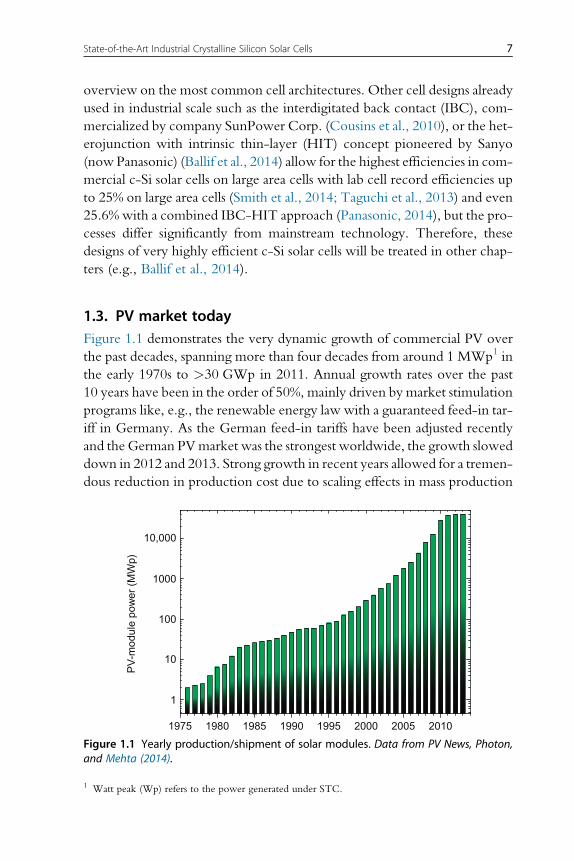
1.3. PV market todayFigure 1.1 demonstrates the very dynamic growth of commercial PV over
the past decades, spanning more than four decades from around 1 MWp1 in
the early 1970s to >30 GWp in 2011. Annual growth rates over the past
10 years have been in the order of 50%, mainly driven by market stimulation
programs like, e.g., the renewable energy law with a guaranteed feed-in tar-
iff in Germany. As the German feed-in tariffs have been adjusted recently
and the German PVmarket was the strongest worldwide, the growth slowed
down in 2012 and 2013. Strong growth in recent years allowed for a tremen-
dous reduction in production cost due to scaling effects in mass production
1975
1
10
100
1000
PV
-mod
ule
pow
er (
MW
p)
10,000
1980 1985 1990 1995 2000 2005 2010
Figure 1.1 Yearly production/shipment of solar modules. Data from PV News, Photon,and Mehta (2014).
1 Watt peak (Wp) refers to the power generated under STC.
7State-of-the-Art Industrial Crystalline Silicon Solar Cells
as well as new and optimized processing technologies. This so-called
learning curve effect of PV resulted in an average module price reduction
of around 20% for every doubling of cumulated PV production (Nemet
and Husmann, 2012). The continuing reduction in processing costs
results in costs of a kWh generated by PV being now in the range of elec-
tricity generated from fossil fuels (depending on the installation site) (Kost
et al., 2013).
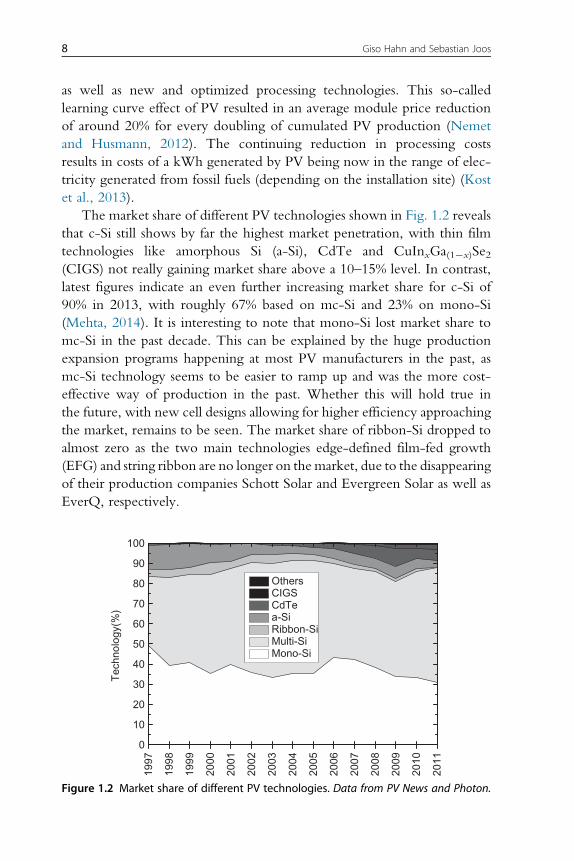
The market share of different PV technologies shown in Fig. 1.2 reveals
that c-Si still shows by far the highest market penetration, with thin film
technologies like amorphous Si (a-Si), CdTe and CuInxGa(1�x)Se2(CIGS) not really gaining market share above a 10–15% level. In contrast,
latest figures indicate an even further increasing market share for c-Si of
90% in 2013, with roughly 67% based on mc-Si and 23% on mono-Si
(Mehta, 2014). It is interesting to note that mono-Si lost market share to
mc-Si in the past decade. This can be explained by the huge production
expansion programs happening at most PV manufacturers in the past, as
mc-Si technology seems to be easier to ramp up and was the more cost-
effective way of production in the past. Whether this will hold true in
the future, with new cell designs allowing for higher efficiency approaching
the market, remains to be seen. The market share of ribbon-Si dropped to
almost zero as the two main technologies edge-defined film-fed growth
(EFG) and string ribbon are no longer on themarket, due to the disappearing
of their production companies Schott Solar and Evergreen Solar as well as
EverQ, respectively.
1997
1998
1999
2000
2001
2002
2003
2004
2005
2006
2007
2008
2009
2010
2011
0
10
20
30
40
50
60
70
80
90
100
Tec
hnol
ogy(
%)
OthersCIGSCdTea-SiRibbon-SiMulti-SiMono-Si
Figure 1.2 Market share of different PV technologies. Data from PV News and Photon.
8 Giso Hahn and Sebastian Joos

1.4. Basic structure of an industrial c-Si solar cellA schematic of the basic structure for a typical state-of-the-art industrial c-Si
solar cell is shown in Fig. 1.3. The base is p-type material, moderately
B doped to a resistivity of around 1 Ω cm (NA¼1.5�1016 per cm3). The
emitter is n++-doped2 using P with high surface concentration ND>1020
per cm3, and the front surface is textured to allow a better incoupling of
impinging photons (lower reflectivity). The emitter is covered by a thin
dielectric layer of H-rich silicon nitride (SiNx:H), acting as antireflective
coating (ARC), surface passivation layer, and reservoir of H. On the front,
the metallization finger grid is realized by Ag paste, fired through the SiNx:H
layer at high temperature. On the rear, a full area contact is realized by Al
paste, which forms an alloy with Si during the firing step, resulting in an
Al doped p+-region (around 1019 per cm3) at the rear after cool down to
room temperature (back surface field, BSF). To allow interconnection of
the individual cells for module integration using soldering, stripes or pads
of Ag/Al paste are used at the rear side, as Al is not solderable. The complete
cell thickness is around 180 μm (note that features shown in Fig. 1.3 are not
to scale). The formation of the respective regions of the cell will be dealt
with in more detail in the following sections.
The use of H-rich SiNx:H layers for PV (Morita et al., 1982) in the
so-called “firing through SiNx:H process” has been pioneered by Kyocera
(Kimura, 1984; Takayama et al., 1990) and Mobile Solar for their EFG
ribbon-Si material (Cube and Hanoka, 2005). In the 1990s, other companies
and research institutes like, e.g., IMEC (Szlufcik et al., 1994) and others devel-
oped the process further. The breakdown of costs for c-Si module production
in Fig. 1.4 reveals that wafer and module costs are the dominating factors.
hν
Al
Ag
p-Sin+
p+
SiNx:H
Electron
Hole
Figure 1.3 Schematic basic structure of an industrial c-Si solar cell in cross section (notto scale).
2 The superscripts + and ++ indicate a high and a very high doping concentration, respectively.
9State-of-the-Art Industrial Crystalline Silicon Solar Cells

Excellent early (e.g., Szlufcik et al., 1997) and more recent (e.g., Gabor,
2012; Neuhaus andMunzer, 2007) review papers on low-cost industrial c-Si
solar cell fabrication exist, forming the base of this chapter. Since then new
technologies have emerged, allowing for a reduction of costs as well as effi-
ciency losses and therefore an increase of efficiency in mass production. To
tackle these losses, the next section will describe the physics involved in the
operation principle of a solar cell.
2. OPERATION PRINCIPLE OF A c-SI SOLAR CELL
2.1. Band diagramThe fundamental operation principle of a c-Si solar cell is visualized in the
band diagram shown in Fig. 1.5. The doping gradient due to the abrupt
change in doping concentration at the pn-junction results in electrons (free
majority carriers in the n-region) diffusing from the n-region into the
p-region and holes (free majority carriers in the p-region) diffusing into
the n-region. The remaining ionized doping atoms at lattice sites (positively
charged in the n-region, negatively charged in the p-region) form the space
charge region (SCR) extending into both sides of the pn-junction. The
electric field hinders the free carriers to completely diffuse into the regions
of opposite doping, when equilibrium between diffusion and drift current of
free carriers is reached. The built-up electric field causes bending of the
energy bands, with the Fermi energyEF as defined by the Fermi–Dirac func-
tion at a constant level (a horizontal line) in both regions.
Upon illumination, absorbed photons excite electrons from the valence
band to the conduction band via the internal photoelectric effect.
36%26%
38%
WaferCell productionModule
Figure 1.4 Breakdown of c-Si PV module manufacturing costs. Data from Goodrich et al.(2013).
10 Giso Hahn and Sebastian Joos

Absorption of one photon therefore generates an electron–hole pair, as the
missing electron in the valence band is referred to as a hole. Free electrons
and holes can diffuse until they recombine or reach the SCR. Here, charge
carriers of different types are separated, electrons are accelerated into the
n-region, holes into the p-region. In case of illumination, the semiconductor
is not in thermal equilibrium anymore, and the relation for electron and hole
concentrations n0 and p0, respectively, as defined for thermal equilibrium
(without illumination or applied voltage)
n0p0¼ n2i , (1.1)
(with intrinsic carrier concentration ni) is not valid anymore and becomes
np¼ n2i expEFn�EFp
kT
� �> n2i , (1.2)
with n and p being electron and hole concentrations, respectively. As both
electron and hole concentrations are increased when the semiconductor is
illuminated, two separate Fermi–Dirac functions for each carrier type have
to be defined, with two resulting Fermi levels EFn and EFp referred to as
quasi-Fermi levels of electrons and holes.
Metal contacts with EF at roughly the same energetic position as for the
majority carriers in the contacted Si region can extract carriers from both
regions. The contact for the p-type region as depicted in Fig. 1.5 is ohmic,
whereas the n-type contact is of Schottky-type (energy barrier for electrons).
Metal p-type Si n-type Si Metal
hν
Energy
Valence band
E
Conduction band
SCR
EF
EF
Electron
Hole
Figure 1.5 Schematic band diagram of a c-Si solar cell with pn-junction, space chargeregion (SCR), photon absorption, charge carrier generation, and separation. Quasi-Fermilevels and EF in the metal contacts are indicated as well.
11State-of-the-Art Industrial Crystalline Silicon Solar Cells

The barrier can be overcome via tunneling, provided it is thin enough and
not too high.
2.2. Solar cell parametersAn ideal solar cell can be described by a 1-diode model and the j–V char-
acteristic of an illuminated diode
j¼ j0 expqV
kT
� ��1
� �� jl, (1.3)
with current density j, saturation current density j0, elementary charge q,
Boltzmann’s constant k, and light-generated current density jl. j0 is defined as
j0¼ qDnn2i
LnNA
+qDpn
2i
LpND
, (1.4)
withDn (Dp) the diffusion constant of electrons (holes),NA (ND) the doping
density of acceptors (donors) and Ln (Lp) the minority charge carrier diffu-
sion length of electrons (holes).
The resulting j–V curve is shown in Fig. 1.6. The maximum current
density at V¼0 is the short circuit current density j jscj¼ jl. The point of
maximum power density (mpp) is also indicated, with the fill factor FF
defined as
Current density/power density
Output power
Voltage
Dar
k cu
rve
Illum
ina
ted
curv
e
Short circuit current density
Open-circuit voltage
Maximum powerpoint (MPP)
VocVmpp
jsc
jmpp
Figure 1.6 Dark and illuminated j–V curve of a solar cell as well as output power independence of voltage.
12 Giso Hahn and Sebastian Joos

FF¼ jmppVmpp
jscVoc
, (1.5)
resulting with the impinging photon power density pphot of photons with
energy Ephot in the efficiency
η¼ jscVocFF
pphot: (1.6)
2.3. Fundamental efficiency limit of an ideal c-Si solar cellIn a semiconductor with band gap Eg (1.12 eV at 25 �C for c-Si), photons
with energy E>Eg can be absorbed, creating electron–hole pairs, while
photons with E<Eg cannot be absorbed and are transmitted, see Fig. 1.7.
Generation of electron–hole pairs by illumination is a non-equilibrium pro-
cess with some of the carriers occupying states high in the conduction band
(electrons) and deep in the valence band (holes) directly after generation
depending on the photon energy. The generated electrons and holes reach
thermal equilibrium via collisions with other charge carriers or phonons
within the femtosecond (fs) range (thermalization). Afterward, they occupy
states close to the band edges according to Fermi–Dirac statistics. The max-
imum voltage reachable (open circuit voltage Voc of the cell) is limited by
splitting of the quasi-Fermi levels for electrons and holes ΔEF, with
1. 2.
Ene
rgy
ΔEF qVmpp
3. 4.
hν hν
Figure 1.7 Fundamental loss mechanisms for an ideal pn-junction based solar cell. 1.Transmission Ephot<Eg, 2. Thermalization Ephot>Eg, 3. Quasi-Fermi level splittingΔEF<Eg, and 4. Voltage at mpp Vmpp<Voc.
13State-of-the-Art Industrial Crystalline Silicon Solar Cells

ΔEF<Eg. As the maximum power point (mpp) of the illuminated j–V curve
(Fig. 1.6) is between V¼0 (maximum j¼ jsc) and j¼0 (maximum V¼Voc),
Vmpp is always<Voc. These four fundamental loss mechanisms limit the
maximum efficiency of an ideal c-Si solar cell under STC to 29.4%
(Richter et al., 2013).
2.4. Two-diode modelA real solar cell can be described by an equivalent circuit containing two
diodes, with the addition of series resistance Rs, shunt resistance Rsh and a
second diode accounting for recombination in the SCRwith an ideality fac-
tor generally assumed to be 2 (Fig. 1.8).
j¼ j01 expq V � jRsð Þ
kT
� ��1
� �+ j02 exp
q V � jRsð Þ2kT
� ��1
� �+
V � jRsð ÞRsh
� jl:
(1.7)
Contributions to Rs are ohmic resistive losses in emitter, base, and met-
allization as well as the contact resistance between semiconductor and metal.
Finite Rsh values are caused by alternative current paths short circuiting the
diode (e.g., around the cell’s edge, by a damaged emitter or current paths
through the SCR).
Apart from ohmic losses, recombination of generated charge carriers can
occur, limiting performance of the solar cell.
2.5. Radiative recombinationRadiative recombination refers to direct band-to-band transitions of an elec-
tron from the conduction band to the valence band while emitting a photon.
It is the inverse process of photon absorption. The generated excess charge
carrier density Δn with
n¼ n0 +Δn and p¼ p0 +Δn (1.8)
j01
jI
j02
RS
RSh
Figure 1.8 Equivalent circuit of a real pn-junction solar cell.
14 Giso Hahn and Sebastian Joos

can be reduced due to recombination of charge carriers with a recombina-
tion rate R defining the lifetime τ of excess charge carriers
τ¼ΔnR
: (1.9)
c-Si is an indirect band gap semiconductor. In addition to an electron (in the
conduction band) and a hole (in the valence band), a phonon is necessary for
the band-to-band transition to occur due to conservation of momentum.
Therefore, this mechanism is not probable and can normally be neglected
in c-Si. With the radiative recombination coefficient crad, the net rate Rrad
for this type of recombination becomes3
Rrad¼ crad np�n2i� �
, (1.10)
resulting for low injection (Δn much lower than doping concentration4) in
the radiative lifetime
τrad¼1
cradp0(1.11)
for p-doped material.
2.6. Auger recombinationInstead of creating a photon, the energy of the recombination process can be
used to excite another existing free charge carrier (an electron in the con-
duction band or a hole in the valence band). This charge carrier thermalizes
after excitation toward the band edge, converting the recombination energy
into phonons. With the Auger recombination coefficients cA,n and cA,p for
electrons and holes, respectively, the Auger recombination rate reads
RA ¼ cA,nn np�n2i� �
+ cA,pp np�n2i� �
: (1.12)
As above, for low injection we obtain the Auger lifetime for p-doped
material
τA ¼ 1
cA,pp20
: (1.13)
3 Note that we are only interested in the recombination rate of the excess charge carriers (therefore
np�ni2, subtracting recombination occurring also in thermal equilibrium).
4 At room temperature, all dopants are assumed to be ionized (NA¼p0 in p-type material), and therefore
Δn�p0 for low injection.
15State-of-the-Art Industrial Crystalline Silicon Solar Cells

Auger recombination as a three-particle process is only relevant for high
doping concentrations >1017 per cm3 in standard industrial solar cells.
2.7. SRH recombinationEnergy levels in the band gap can trap free charge carriers and cause a very
effective recombination mechanism, especially when their energetic posi-
tion is close to mid-gap. This type of recombination was formulated by
Shockley, Read, and Hall (Hall, 1952; Shockley and Read, 1952), using sta-
tistics of capture and emission of free carriers and is therefore referred to as
SRH recombination. Its recombination rate
RSRH¼ np�n2i� �
τp n0 + n1 +Δnð Þ+ τn p0 + p1 +Δnð Þ (1.14)
with
τp ¼ 1
Ntvpσp, τn¼ 1
Ntvnσn,n1¼ niexp
Et�EFi
kT
� �, p1¼ niexp
EFi�Et
kT
� �,
(1.15)
includes the trap densityNt of the energy levels in the band gap, the thermal
velocity of electrons and holes (vn, vp) and the capture cross sections of the
trap for electrons and holes (σn, σp). Et is the energetic position of the trap
level and EFi the position of the Fermi level in intrinsic c-Si. The SRH
lifetime
τSRH ¼ τp n0 + n1 +Δnð Þ+ τn p0 + p1 +Δnð Þp0 + n0 +Δn
(1.16)
for p-type material (p0�n0), low injection (p0�Δn), and trap energy levelat mid-gap (Et¼EFi) reads
τSRH¼ τn¼ 1
Ntvnσn(1.17)
and is inversely proportional to the trap density as well as the thermal veloc-
ity and capture cross section of the minority carriers (electrons in p-type
material).
All recombination channels are acting in parallel, and the resulting bulk
lifetime τb is given by
16 Giso Hahn and Sebastian Joos
1
τb¼ 1
τrad+
1
τA+
1
τSRH
: (1.18)
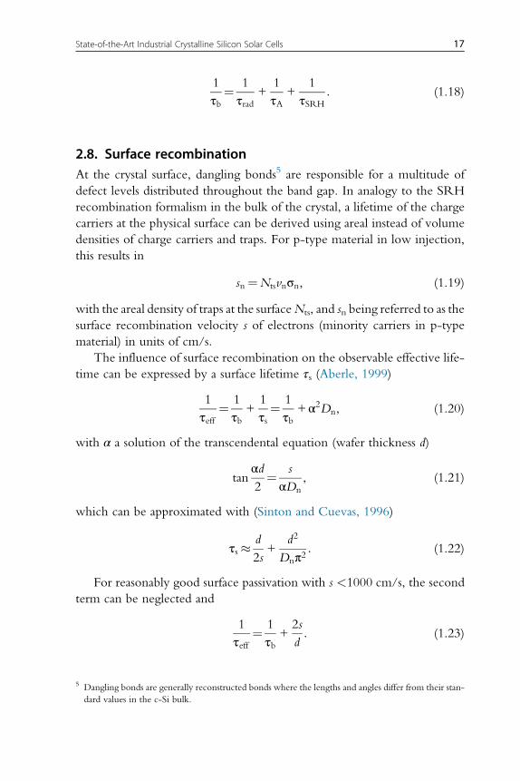
2.8. Surface recombinationAt the crystal surface, dangling bonds5 are responsible for a multitude of
defect levels distributed throughout the band gap. In analogy to the SRH
recombination formalism in the bulk of the crystal, a lifetime of the charge
carriers at the physical surface can be derived using areal instead of volume
densities of charge carriers and traps. For p-type material in low injection,
this results in
sn¼Ntsvnσn, (1.19)
with the areal density of traps at the surfaceNts, and sn being referred to as the
surface recombination velocity s of electrons (minority carriers in p-type
material) in units of cm/s.
The influence of surface recombination on the observable effective life-
time can be expressed by a surface lifetime τs (Aberle, 1999)
1
τeff¼ 1
τb+
1
τs¼ 1
τb+ α2Dn, (1.20)
with α a solution of the transcendental equation (wafer thickness d)
tanαd2¼ s
αDn
, (1.21)
which can be approximated with (Sinton and Cuevas, 1996)
τs � d
2s+
d2
Dnπ2: (1.22)
For reasonably good surface passivation with s <1000 cm/s, the second
term can be neglected and
1
τeff¼ 1
τb+2s
d: (1.23)
5 Dangling bonds are generally reconstructed bonds where the lengths and angles differ from their stan-
dard values in the c-Si bulk.
17State-of-the-Art Industrial Crystalline Silicon Solar Cells

2.9. Recombination and saturation current densityRecombination reduces the maximum current density jsc of the solar cell, as
only minority charge carriers generated within roughly one diffusion length
on either side of the pn-junction reach the junction and are injected into the
region on the opposite side of the junction. But from Eq. (1.3) also strong
influence of j0 on Voc can be seen, as for j¼0
Voc¼ kT
qln
jl
j0+ 1
� �� kT
qln
jl
j0
� �: (1.24)
As the diffusion lengths of both types of carriers in Eq. (1.4) are linked to
recombination via the lifetime of the minority charge carriers
Ln,p ¼ffiffiffiffiffiffiffiffiffiffiffiffiffiffiffiDn,pτeff
p, (1.25)
maximizing the effective lifetimes in emitter and base is crucial for improv-
ing solar cell performance. Effective lifetime is affected by bulk lifetime and
surface recombination velocity (Eq. 1.23), therefore good solar cells should
combine a high τb (low recombination in bulk and emitter) and good surface
passivation on emitter and base to reduce s.
2.10. Optical lossesIf all impinging photons with Ephot>Eg were absorbed in the solar cell, with
all of these photons contributing to the extracted current density, the max-
imum jsc would be around 44 mA/cm2 under STC. Apart from recombina-
tion losses described above, another fraction is lost due to optical losses.
These losses include reflection at the front side (metal grid and ARC),
absorption in the metal and ARC, absorption via free carrier absorption
(FCA)6 and photons not being absorbed in c-Si (mostly long wavelengths
photons7) leaving the cell.
The different loss mechanisms are visualized in Fig. 1.9, where they are
separated into optical and electrical losses.
6 Free carrier absorption is the absorption of a photon by an electron in the conduction band or a hole in
the valence band without generation of additional free carriers. It is important in highly doped areas
(emitter and BSF).7 The absorption coefficient in c-Si with indirect bandgap leads to an absorption coefficient strongly
varying with wavelength, leading for photons with wavelengths >1000 nm to absorptions lengths
>200 μm.
18 Giso Hahn and Sebastian Joos
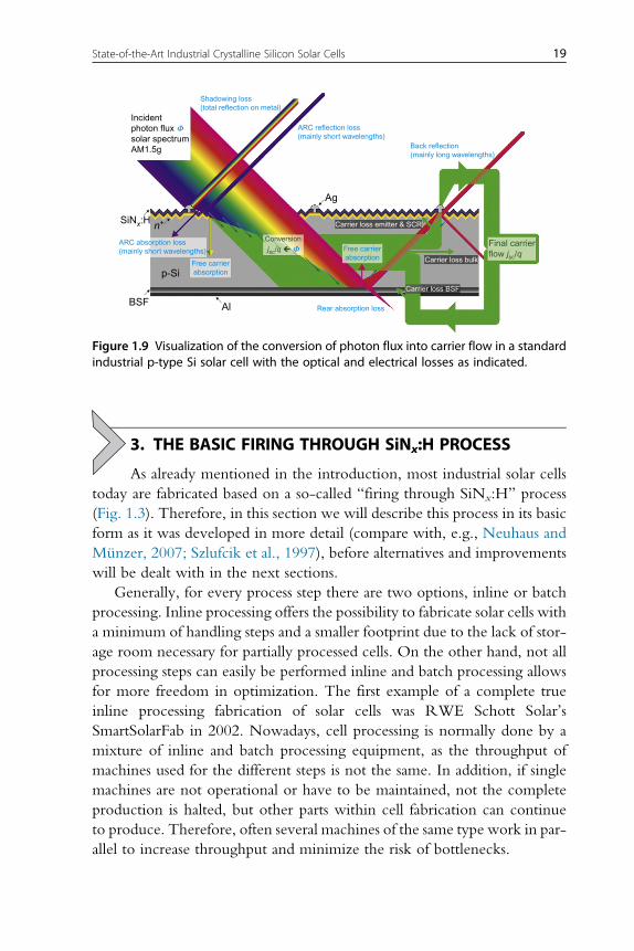
3. THE BASIC FIRING THROUGH SiNx:H PROCESS
As already mentioned in the introduction, most industrial solar cells
today are fabricated based on a so-called “firing through SiNx:H” process
(Fig. 1.3). Therefore, in this section we will describe this process in its basic
form as it was developed in more detail (compare with, e.g., Neuhaus and
Munzer, 2007; Szlufcik et al., 1997), before alternatives and improvements
will be dealt with in the next sections.
Generally, for every process step there are two options, inline or batch
processing. Inline processing offers the possibility to fabricate solar cells with
a minimum of handling steps and a smaller footprint due to the lack of stor-
age room necessary for partially processed cells. On the other hand, not all
processing steps can easily be performed inline and batch processing allows
for more freedom in optimization. The first example of a complete true
inline processing fabrication of solar cells was RWE Schott Solar’s
SmartSolarFab in 2002. Nowadays, cell processing is normally done by a
mixture of inline and batch processing equipment, as the throughput of
machines used for the different steps is not the same. In addition, if single
machines are not operational or have to be maintained, not the complete
production is halted, but other parts within cell fabrication can continue
to produce. Therefore, often several machines of the same type work in par-
allel to increase throughput and minimize the risk of bottlenecks.
AlBSF
SiNx:H
p-Si
Ag
n+
ARC absorption loss(mainly short wavelengths)
ARC reflection loss(mainly short wavelengths)
Shadowing loss(total reflection on metal)
Free carrierabsorption
Rear absorption loss
Back reflection(mainly long wavelengths)
Carrier loss BSF
Carrier loss bulk
Free carrierabsorption
Final carrierflow jsc/q
Carrier loss emitter & SCR
Incident photon flux Fsolar spectrum AM1.5g
Figure 1.9 Visualization of the conversion of photon flux into carrier flow in a standardindustrial p-type Si solar cell with the optical and electrical losses as indicated.
19State-of-the-Art Industrial Crystalline Silicon Solar Cells

3.1. Wafer washing, texturization, and cleaningAfter crystallization, mono-Si and mc-Si wafers are sliced out of the Si ingot
using wire saws, containing slurry with abrasives for cutting into the Si
(Dold, 2014). This leaves, apart from contaminants, saw damage on both
sides of the Si wafer with a depth in the range of up to 10 μm (depending
on sawing conditions). After wafer washing, this saw damage has to be
removed, as the disturbed region of the crystal (cracks, dislocations) is of
poor electronic quality.
For mono-Si, this is done in an alkaline wet chemical solution of KOH
and isopropyl alcohol (IPA) at temperatures of around 80 �C. The KOH
solution etches the Si while the alcohol masks the surface randomly. Etching
is anisotropic, with the result that the most densely packed crystal planes in
c-Si have the slowest etch rate (the (111)-planes). If the wafer is (100)-
oriented, the four (111) orientations in the diamond lattice of c-Si will ran-
domly form square-based upright pyramids (Fig. 1.10). These pyramids very
effectively reduce the reflectivity of the surface and therefore increase the
incoupling of photons into c-Si. The etching reaction can be summarized as
Si + 2H2O+HO�!HSiO3� +2H2 (1.26)
and consists of oxidation of Si, formation of a solvable salt and dissolving the
salt in water (Neuhaus and Munzer, 2007).
The surface is increased after random pyramid texturing by a factor of
�1.7, which has consequences for surface passivation and saturation current
densities of the emitter and the SCR.
mc-Si does not offer a well-defined grain orientation at the wafer surface,
as the grains are randomly distributed. Therefore, other texturing solutions
had to be developed. Standard is an acidic solution based on HF and HNO3
without further additives (Einhaus et al., 1997; Hauser et al., 2003). The tex-
ture attacks the Si surface first at areas where not all Si bonds are perfectly
saturated. Therefore, the saw damage is needed for a non-uniform attack
of the surface. Existing surface defects like cracks are widened and a
“worm-like” structure is formed (Fig. 1.10). Once the saw damage is etched
away, the textured surface starts to flatten again for prolonged processing
times, as sharp edges are rounded. Four to five micrometer removal of Si
per side is normally enough to remove the saw damage and obtain a low
reflectivity.8 The etching reaction takes place in two steps, an oxidation
8 Note that the maximum depth of saw damage can be up to around 10 μm, but as predominantly the
damaged areas are attacked, less overall removal of Si is needed.
20 Giso Hahn and Sebastian Joos

3Si + 4HNO3! 3SiO2 + 3H2O+4NO (1.27)
followed by etching of the SiO2
3SiO2 + 18HF! 3H2SiF6 + 6H2O: (1.28)
Afterward, the thin porous Si layer at the surface is etched off in (cold)
KOH. The remaining reflectivity is significantly higher than for random
pyramids, therefore it is not used for mono-Si (Fig. 1.11). Acidic texturing
can be done elegantly inline, as texturing time is in the range of only around
2 min (depending on temperature) (Hauser et al., 2004; Neuhaus and
Munzer, 2007).
Figure 1.10 SEM images of textured c-Si surfaces for mono-Si using KOH/IPA (left) andmc-Si using an acidic texture solution (right).
400 600 800 1000 12000.0
0.1
0.2
0.3
0.4
0.5
0.6
0.7
Ref
lect
ance
Wavelength (nm)
Bare SiSi texturedBare Si AR coatedSi textured and AR coated
Figure 1.11 Reflectivity of bare Si and alkaline-textured mono-Si with and withoutSiNx:H ARC.
21State-of-the-Art Industrial Crystalline Silicon Solar Cells
After texturing, the wafers are thoroughly cleaned as the next step is the
diffusion taking place at high temperatures. Impurities present on the wafer
surface could diffuse in to the wafer causing recombination and therefore
lowering τb. Cleaning normally consists of rinsing in deionized (DI) water,
cleaning in HCl, DI water rinsing, etching in HF to form a hydrophobic
surface, followed by a short dip in DI water and drying.
3.2. Phosphorus diffusionIn this step, the heart of the solar cell, the pn-junction, is formed. The two
most common ways to form the P-doped emitter will be described in the
following.
In most cases, the in-diffusion of P into c-Si takes place in a quartz tube
furnace. N2 is directed into a bottle (bubbler) containing POCl3, which is
liquid at room temperature. POCl3 molecules are transported with the N2
flow into the quartz tube, where the wafers are located in quartz containers
(boats) with spacing between thewafers at temperatures around 800–850 �C.O2 is added and on the wafer surface P2O5 is formed according to
4POCl3 + 3O2 ! 2P2O5 + 6Cl2, (1.29)
where the formed Cl2 provides an additional cleaning effect on the wafer
surface. TheO2 flow also oxidizes the Si surface, and the resulting SiO2 layer
together with the P2O5 forms the so-called phosphor silicate glass (PSG)
layer acting as the diffusion source. P diffuses into c-Si and the diffusion
coefficient depends strongly on doping concentration, as the level of EF
determines the amount of vacancies present in the material. For
P concentrations well above 1019 per cm3 at diffusion temperature, a differ-
ent diffusivity is observed due to the existence of double negatively charged
vacancies in large amounts, forming a mobile quasi-particle with ionized P+.
For P concentrations below 1019 per cm3, single negatively charged vacan-
cies dominate the diffusion mechanism. This results in the characteristic
kink-and-tail shaped profile of P diffusion in c-Si whereby the tail is formed
due to the “normal” diffusionmechanism involving vacancies (Fair and Tsai,
1977). During diffusion, time, temperature, and gas flows have an influence
on the diffusion profile formed. To increase (double) the throughput, wafers
are often loaded in the quartz boats back-to-back.
As an alternative to quartz tube POCl3 diffusion, a liquid P-containing
layer can be deposited on the wafer surface (mainly diluted H3PO4), e.g., by
spraying. Wafers then move horizontally through a conveyor belt firing
22 Giso Hahn and Sebastian Joos

furnace. As for this inline technique, the time allowed for diffusion is limited
due to throughput and length of the furnace possible, diffusion temperatures
are normally higher than for POCl3 diffusion, resulting in steeper P doping
profiles. Higher doping concentrations normally result in lower emitter
quality and more Auger recombination, increasing the saturation current
density contribution of the emitter j0e. In addition, surface passivation is
influenced by doping concentration with better passivation quality possible
for lowly doped surfaces (Cuevas et al., 1996).
Only P atoms on Si lattice sites are electrically active dopants. The surface
concentration of P in c-Si for an unlimited source is given by the solubility
limit in the range of 3–61020 per cm3 between 800 and 900 �C with
higher values for higher temperatures (Trumbore, 1960). Apart from the
electrically active P atoms, interstitial P or P-containing clusters can form,
increasing the amount of P present in Si especially close to the surface
(Fig. 1.12) (Bentzen et al., 2006a). The almost flat shape of the P doping
profile with electrically active P concentration above 1020 per cm3 is also
referred to as “dead layer,” as this layer is highly recombination active.
Although the high surface concentration of P close to the surface is limiting
the electronic quality, it seems to be needed for the formation of a good low
resistivity contact with the front metal Ag paste during the firing step.
An important parameter of the emitter is its conductivity, as charge car-
riers have to flow laterally toward the collecting finger grid. As the emitter is
a very thin layer (usually well below 1 μm thick), a sheet resistivity is defined
for a uniformly doped layer as
Figure 1.12 P profiles of identical P diffusions in c-Si measured by ECV (electricallyactive concentration) and SIMS (total concentration). The solubility limit at diffusiontemperature according to Bentzen et al. (2006b) and Solmi et al. (1996) is also indicated.
23State-of-the-Art Industrial Crystalline Silicon Solar Cells

Rsheet¼ ρ
d(1.30)
where ρ is the resistivity of the layer with thickness d.
For non-uniformly doped layers as is the case for a diffusion profile, sheet
resistivity calculates according to
Rsheet ¼ 1Ð d0
1
ρ zð Þdz, (1.31)
with depth z. Typical values ofRsheet for P diffusions are 50–100 Ω/sq. Note
that carrier mobility is a function of doping concentration, therefore also
conductivity is a function of doping density.
3.2.1 Phosphorus diffusion gettering of impuritiesDuring P diffusion, SiO2 is formed at the wafer surface. For the formation of
SiO2 Si, atoms have to leave their lattice sites, and a flux of Si interstitials Sii is
generated. In addition, diffusing P atoms change position with a Si atom on
lattice site (Sis), further increasing the concentration of Sii. These Si inter-
stitials themselves can change position with an impurity atom (M) located at
lattice sites via a “kick-out reaction”
Sii +Ms ! Sis +Mi: (1.32)
In interstitial form, the impurity atom is mobile and can diffuse through
the crystal toward a location with higher solubility. Such a location of high
solubility can, e.g., be the highly doped region containing precipitated
P close to the surface or the PSG (Bentzen et al., 2006a). Such regions
are called getter sinks. Due to the presence of regions with high solubility
for impurity atoms, a concentration gradient is formed toward the sink,
resulting in more and more impurity atoms moving toward the sink, leaving
a cleaner region behind. This self-cleaning process is called gettering of
impurities. Depending on the location of the getter sink we distinguish
between external gettering (e.g., at the crystal surface, where the impurities
can be removed) or internal gettering at extended defects in the Si bulk (e.g.,
at grain boundaries, dislocations, or precipitates). The gettering process in
general can be divided into three phases: (1) freeing the impurity from its
(bonded) position by supplying an activation energy, (2) diffusion of the
impurity in the wafer, (3) capture of the impurity at the gettering location.
Depending on the specific mechanism present, it is distinguished between
24 Giso Hahn and Sebastian Joos
relaxation induced, segregation induced, and injection induced gettering,
where also combinations of these different mechanisms are possible (Kang
and Schr€oter, 1989; Seibt and Kveder, 2012).
It could be shown that for back-to-back diffusion the positive gettering
effect is less pronounced, as only one effective external getter sink is available
(Schneider et al., 2005). The same can be assumed for inline diffusion, as the
diffusion source is applied only on one side.9
3.3. Edge isolationAfter P diffusion, the PSG layer is etched in dilute HF and impurities
gettered toward the PSG are removed.
As the highly doped emitter is still present around the wafer edges and at
the rear side, it will cause a short circuiting of the diode. It either has to be
removed, or the connection between front and rear side has to be inter-
rupted later in the process (e.g., by laser scribing; Emanuel et al., 2001).
An elegant way to remove the rear side emitter is by inline etching of the
rear side with the wafer floating on the etch solution containing H2O,
HF, HNO3, and H2SO4. As the PSG etch can be performed inline as well,
both steps can be combined in a single inline wet bench (Delahaye et al.,
2004; Melnyk et al., 2005). Thereby care has to be taken that the emitter
on the front side is not attacked by the etch solution or the atmosphere con-
taining reactive species.
3.4. SiNx:H depositionTo further minimize reflection losses at the front side, an ARC based on
SiNx:H is deposited on the front.10 For normal incidence of photons,
destructive interference is reached if the thickness d of the ARC is
d¼ λ
4nSiN, (1.33)
with wavelength λ and refractive index of the SiNx:H layer nSiN. Fresnel’s
equations predict a zero reflectivity if
nSiN ¼ ffiffiffiffiffiffiffiffiffiffiffinairnSi
p, (1.34)
9 For back-to-back POCl3 diffusion and inline diffusion, a weak P diffusion is also observed at the rear
side, by transport of P atoms via the gas phase.10 The notation SiNx:H is used, as the silicon nitride layers are not of stoichiometric composition and
contain significant amounts of H.
25State-of-the-Art Industrial Crystalline Silicon Solar Cells

with nair and nSi refractive indices of air and c-Si being the materials above
and below the ARC, respectively. With nSi(600 nm)¼4, on cell level the
optimum refractive index would be nSiN¼2. As the cells are later encapsu-
lated into modules using ethylene vinyl acetate (EVA) with refractive index
around 1.5, a slightly higher nSiN would be optimum for solar cells in mod-
ule application. With Eqs. (1.33) and (1.34) typical ARC thicknesses are
75–80 nm for nSiN¼2, if reflectivity of photons with λ¼600–650 nm
(the maximum in photon flux of the AM1.5g spectrum) should be
minimized.
Apart from the ARC effect, SiNx:H is also suited for surface passivation
of the n++ P-doped emitter. Defects located close to the c-Si/SiNx:H inter-
face in the SiNx:H layer provide fixed positive charges in the order of 1012–
1013 per cm2 (Aberle, 1999; Lamers et al., 2012). The minority charge car-
riers (holes in n-type material) are repelled from the surface due to Coulomb
repulsion while majority carriers are attracted, and therefore recombination
is lowered.11 This surface passivation mechanism is referred to as field effect
passivation in contrast to chemical passivation, where the reconstruction of
chemical bonds lowers the density of energy levels in the bandgap. Chemical
passivation is also present for SiNx:H layers, but remaining defect densities
are usually higher than for SiO2 layers, which in turn have a lower density of
fixed charges.
If the SiNx:H layer contains significant amounts of H, this H can be
released during the firing step and diffuse into the c-Si bulk (Hahn et al.,
2004; Jiang et al., 2003). Here, H can passivate bulk defects and drastically
improve material quality (Duerinckx and Szlufcik, 2002; Hahn et al., 2010).
This is a crucial step especially for mc-Si material with high defect densities.
The most common technology to deposit SiNx:H layers is plasma-
enhanced chemical vapor deposition (PECVD). There are direct and remote
plasma techniques available. A direct plasma system usually operates at low
frequency of 40 kHz. The wafer forming one electrode is in contact with the
plasma, and accelerated ions can bombard the wafer surface leading to a cer-
tain surface damage.12 These systems usually operate in batch mode. In
remote plasma systems, operating usually at high frequencies around
13.56 MHz, the plasma is spatially separated from the wafer, and a linear
plasma source is used with microwaves supplying the excitation. Remote
plasma systems are usually operating in inline geometries with the wafers
11 Note that recombination rate is dependent on np in Eqs. (1.10), (1.12), and (1.14).12 This surface damage is not necessarily negative, as it can provide a reservoir for H.
26 Giso Hahn and Sebastian Joos

lying on trays being transported through the reactor underneath the linear
plasma source. For both techniques, pressure is around 0.1–1 mbar and
deposition temperature is between 300 and 450 �C, depending on technol-
ogy. Precursor gases used are SiH4 and NH3, and the SiH4/NH3 ratio deter-
mines the stoichiometry and therefore refractive index and absorption
coefficient of the resulting SiNx:H. Higher SiH4/NH3 ratios (Si-rich layers)
lead to higher refractive indices and higher absorption (Nagel et al., 1998).
As absorption in the ARC is unwanted, usually a compromise between opti-
mum nSiN (2.3–2.4 for module application) and low absorption is found,
with nSiN(600 nm)¼2.0–2.1.
Before PECVD SiNx:H with high throughput became available for PV
at the end of the 1990s, TiO2 was often used as ARC for industrial c-Si cells.
Compared to SiNx:H, a higher refractive index without significant absorp-
tion was possible, but TiO2 layers showed poor surface passivation qualities
and contained noH needed for bulk passivation. Themethod used for depo-
sition was atmospheric pressure chemical vapor deposition (APCVD).13
3.5. Metallization via screen-printingScreen-printing of metal pastes for PV application is a very robust method
already introduced in 1975 (Ralph, 1975) and can be used as an inline pro-
cess.14 A conveyor belt transports the wafer onto the printing chuck.
A screen consisting of a mesh of wires partly covered with an emulsion is
the mask for the metallization process. Metal paste is printed through the
openings in the emulsion through the mesh of wires onto the wafer lying
under the screen. The screen is positioned on top of the wafer with a
well-defined distance between screen and wafer (the snap-off distance).
The paste is placed on top of the screen and a squeegee moving horizontally
without pressure on the screen fills the openings of the mesh uniformly with
paste. In the next horizontal movement of the squeegee over the screen, it is
pressed onto the screen with a defined pressure, pressing the screen locally
against the wafer surface and pushing the paste from the filled areas onto the
wafer surface. The screen snaps off from the wafer after the passing of the
squeegee because of the screen tension (Fig. 1.13). After printing, the wafer
is transported into a drying furnace for evaporation of the volatile ingredients
of the paste at temperatures of around 150–200 �C to avoid smearing of the
paste when it is flipped over to metallize the other surface. Due to the
13 See Richards (2004) for a review on TiO2 and other dielectrics for use of ARC.14 See also Holmes and Loasby (1976) and Neuhaus and Munzer (2007) for more details.
27State-of-the-Art Industrial Crystalline Silicon Solar Cells

tension put on the screen during every printing step, the lifetime of
the screens is limited to several thousand printing steps as they wear out
with time.
3.5.1 Front side metallizationFor front side metallization, the following criteria have to be met by the
paste used: (1) low contact resistance to c-Si, (2) low specific resistance in
the printed structure, (3) no junction shunting, (4) good aspect ratio (height
to width ratio) of the fingers, (5) good adhesion to c-Si, (6) opening of
SiNx:H layer provided, and (7) solderability for cell interconnection in
the module. Ag containing paste (70–80%weight) is used, as Ag is highly con-
ductive and therefore allows for good conductivity in the printed metal fin-
gers. Additional components are glass frits containing PbO, B2O3, and SiO2
(1–10%weight), which are responsible for locally dissolving the SiNx:H layer
Squeegee
Frame
Solar Cell
Closed meshOpen mesh
Metal paste
Vacuum chuck
Figure 1.13 Screen-printing of metal paste.
28 Giso Hahn and Sebastian Joos

as well as for a good adhesion. Also present are organic binders
(15–30%weight), influencing the rheology of the paste which has to be
low enough to ensure that a continuous finger is formed and high enough
to keep a high aspect ratio (Neuhaus and Munzer, 2007).
During the firing step at temperatures around 800 �C, the electrical con-tact between Ag and c-Si is established. Early detailed studies for Ag front
contact formation by Ballif et al. (2002, 2003) and Schubert et al.
(Schubert, 2006; Schubert et al., 2002, 2004) led to the following picture
(Fig. 1.14). Below 600 �Corganic components burn out (A). At higher tem-
perature, the contact is formed as first the PbO melts, wets, and etches the
SiNx:H layer (B). The Ag particles with sizes of several μm sinter together
and form a conductive film. Then a redox reaction between PbO and Si
forms Pb (C). The liquid Pb starts to melt Ag (D), and the Ag/Pb melt reacts
with Si, etching inverted pyramids locally into the c-Si surface (E). On
cooling down Ag recrystallizes on (111)-Si planes, forming isolated contact
points to the emitter (F). The recrystallized Ag points at the c-Si surface can
either be in direct contact with the sintered Ag layer, or the glass layer iso-
lates them from each other. If there is no direct contact established, contact
resistance depends strongly on the thickness of the glass layer formed in
between. Thin layers can be tunneled through, with small (nanoscale) metal
precipitates of Ag and/or Pb/Bi providing additional hopping sites for elec-
trons. The thickness of the isolating glass layer is a very crucial parameter for
achieving low contact resistance in case of no direct connection between Ag
crystallites and sintered Ag layer. Therefore, firing parameters are very
important, with too high peak temperature resulting in thicker glass layers
and too low peak temperature resulting in not completely opened SiNx:H
layers (Schubert, 2006).
As the contact is not formed everywhere underneath the Ag metalliza-
tion printed onto the wafer, the contact resistance is significantly higher than
for contacts established, e.g., via evaporation of Ag directly on c-Si n+ emit-
ters. Typical values for contact resistance of screen-printed Ag on c-Si are
1–10 mΩ cm2 (Schubert, 2006), while values for evaporated contacts are
in the range of 100–200 μΩ cm2 (Fischer, 1994).
3.5.2 Rear side metallizationFor rear side metallization, Al containing pastes containing Al powder, glass
frit, organic binders, and solvents are used. The lower conductivity of Al
compared to, e.g., expensive Ag does not play a role as long as the contact
is formed on the full area rear side. Another very important advantage of Al is
29State-of-the-Art Industrial Crystalline Silicon Solar Cells

the fact that Al is an acceptor in c-Si and can form a good ohmic rear contact
in combination with a highly p+-doped layer, the BSF (Mandelkorn and
Lamneck, 1972). The BSF is formed by alloying during the firing step after
drying of the paste (L€olgen, 1995).A description of the formation process is given in Huster (2005). The
Al/Si phase diagram depicted in Fig. 1.15 shows the composition of the
Al/Si melt dependent on melt temperature. Upon heating up during the fir-
ing step, Al starts to melt at 660 �C. The Al2O3 shells around the Al spheres
stay in shape, but liquid Al can penetrate through the oxide shell locally and
gets in contact with the c-Si surface and other Al particles. Si is dissolved into
the Al melt at that temperature until according to the phase diagram the melt
contains around 17% Si. As the volume in the stable oxide shells stays con-
stant, the amount of Al leaving the shell covering the c-Si surface corre-
sponds to the volume fraction of Si entering the shells to form the correct
concentration according to the phase diagram. During further increase of
temperature, more and more Si is dissolved in the melt. Assuming a peak
firing temperature of 800 �C, the melt contains around 27% of Si. During
cooling down from peak temperature, a part of the Si has to leave the melt
according to the phase diagram. This Si recrystallizes at the c-Si/melt inter-
face. During recrystallization, a small amount of Al is incorporated into the
recrystallized Si lattice according to the solid solubility of Al in Si at that
- g - g
Silver
A B C
D E F
Silver Silver
SilverSilverSilver
Figure 1.14 Schematic contact formation for Ag screen-printing on n++ emitters. AfterSchubert (2006).
30 Giso Hahn and Sebastian Joos
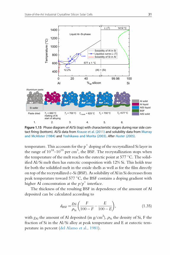
temperature. This accounts for the p+ doping of the recrystallized Si layer in
the range of 1018–1019 per cm3, the BSF. The recrystallization stops when
the temperature of the melt reaches the eutectic point at 577 �C. The solid-ified Al/Si melt then has eutectic composition with 12% Si. This holds true
for both the solidified melt in the oxide shells as well as for the film directly
on top of the recrystallized c-Si (BSF). As solubility of Al in Si decreases from
peak temperature toward 577 �C, the BSF contains a doping gradient with
higher Al concentration at the p/p+ interface.
The thickness of the resulting BSF in dependence of the amount of Al
deposited can be calculated according to
dBSF¼ gAl
ρSi
F
100�F� E
100�E
� �, (1.35)
with gAl the amount of Al deposited (in g/cm2), ρSi the density of Si, F the
fraction of Si in the Al/Si alloy at peak temperature and E at eutectic tem-
perature in percent (del Alamo et al., 1981).
0 20 40 99.98
400
600
800
1000
1200
1400
T6 eut
T2
T4 peak
T5
T3
12.2%
Liquid Al–Si-phase
L (T ) 1414 °C
577 ± 1 °C
(Al) + (Si)
AI Si
Tem
pera
ture
(°C
)
%at silicon
Solubility of Al in SiLiquidus curve L (T )Solubility of Si in Al
100
SiSi wafer
Aluminium paste
Paste dried T2 = 660 �Cmelting of Alstart of alloying
T3 = 700 �C T4 peak = 825 �C
1. 2. 3. 4.
Al solidAl liquidAlSi liquidBSFAlSi solidT5 = 700 �C T6
<577 �C
5. 6.
Figure 1.15 Phase diagram of Al/Si (top) with characteristic stages during rear side con-tact firing (bottom). Al/Si data from Krause et al. (2011) and solubility data from Murrayand McAlister (1984) and Yoshikawa and Morita (2003). After Huster (2005).
31State-of-the-Art Industrial Crystalline Silicon Solar Cells

The p/p+ interface forms a high/low junction, and similar to the
pn-junction the doping gradient is the source for an electric field causing
slight band bending close to the rear metal contact (see Fig. 1.5). This results
in repelling of electrons (minority carriers) and therefore less recombination
at the semiconductor/metal interface in analogy to surface passivation via the
field effect. But as the BSF region is highly doped, its electronic quality
(minority carrier lifetime and diffusion length) is quite low. The effect of
BSF parameters on surface passivation can be calculated via (Godlewski
et al., 1973)
seff ¼ NA
N +A
D+
L +
sbL+
D++ tanh
dBSF
L +
� �
1+sbL
+
D+tanh
dBSF
L +
� � , (1.36)
with seff the effective back surface recombination velocity at the edge of the
quasi-neutral region of the base, NA+, L+, and D+ the acceptor concentra-
tion, the diffusion length, and the diffusion constant of minority carriers in
the BSF, respectively, and sb the surface recombination at the physical back
surface. It can be seen that for low seff, e.g., a high L+ and a low ratio ofNA/
NA+ (high concentration gradient) are beneficial. Therefore, B can bemixed
to the Al paste to increase p+ doping of the BSF, as B has a higher solubility
in Si compared to Al (Rauer et al., 2013).
As cells have to be interconnected for module integration and the Al rear
side is not solderable, a small fraction of the c-Si rear side is metallized with
Ag or Al/Ag paste pads or busbars. These regions have to be kept as small as
possible to avoid unnecessary recombination, as in these regions no BSF is
formed and seff is significantly higher.15 On the other hand they have to be
large enough to assure reliable soldering.
3.5.3 Co-firing stepContact formation is realized in a conveyor belt furnace with optical
heating. The simultaneous contacting of emitter and base in the so-called
co-firing step is a very critical part of the process, as it has to be optimized
for several purposes. During this step, BSF and rear contact are formed,
while in addition on the front side the Ag metallization has to be fired
through the SiNx:H layer, and H has to be released from the SiNx:H layer
into the c-Si bulk to passivate crystal defects. As optimum parameters for
15 Surface recombination velocity of a pure c-Si/metal contact is in the range of 106 cm/s.
32 Giso Hahn and Sebastian Joos

some of these steps are going in different direction of the parameter space, a
compromise has to be found. Ag and Al paste as well as emitter profile and
SiNx:H layer therefore have to be tuned to match their optimum firing
parameters as good as possible and allow for a good overall end result.
In Fig. 1.16, a typical firing profile is shown. (1) the first plateau visible
refers to the temperature of 660 �C, where Ag starts to melt (latent heat).
The peak temperature of around 800 �C (2) is kept for only a few seconds.
During cooling down, another plateau at the eutectic point of 577 �C can be
seen (heat of crystallization) (3).
If edge isolation was not already performed earlier in the process (by sin-
gle side etching or other methods like, e.g., plasma edge isolation), laser edge
isolation close to the cell’s edge at the front side is another option. Here, the
emitter is locally removed by laser heating, and a groove is formed (Emanuel
et al., 2001; Schneiderl€ochner et al., 2003). Hereby active cell area is lost,
slightly compromising the current and therefore efficiency (Hauser
et al., 2001).
3.6. Solar cell characterizationAfter solar cell processing, the j–V characteristics of every cell are measured,
with Voc, jsc and FF determining the conversion efficiency (Eq. 1.6). From
these, the current density and voltage at mpp are determined and solar cells
are classified into bins according to current density classes under mpp con-
ditions to avoid current mismatch in the string of the module when cells are
Figure 1.16 Typical firing profile. Data from Huster (2005).
33State-of-the-Art Industrial Crystalline Silicon Solar Cells

connected in series. In addition, all cells are inspected visually to assure that
only solar cells with the same color end up in a module to achieve homo-
geneous optical appearance. Also the reverse break through characteristic of
the diode is checked by applying reverse bias of 12–15 V to avoid the for-
mation of hot spots, which might cause dangerous local heating (hot spots)
of the cell. This could happen when, e.g., one cell or part of it is shaded in
the module and current is flowing in reverse direction through the string,
leading to destruction of the cell.
j–V characteristics are normally measured using a halogen flash lamp that
can provide a constant power of 1000 W/m2 for around 50 ms, with the
light intensity checked by a monitor cell. The actual temperature of the
solar cell is measured and the voltage is corrected to the temperature of
STC, 25 �C. As for STC, the spectrum should be AM1.5g, which is never
achieved exactly by the flasher system, certified reference solar cells have to
be used for calibration to minimize the effect of spectral mismatch. The cal-
ibration cell should exhibit an external quantum efficiency (EQE) very sim-
ilar to the cell to be measured to avoid errors, especially when introducing
new cell designs (Herguth et al., 2011). Contacting and measurement are
realized using the four point probe setup, with several probes for each bus-
bar simulating the situation after tabbing of the cells for interconnection in
the module.
Solar cell parameters are normally determined under STC conditions,
but solar modules under realistic operation conditions in the field might
operate at significantly different temperatures. Depending on the location
of operation, solar cell temperatures well above 25 �C are reached, reducing
the efficiency mainly according to the temperature behavior of the voltage.
This should be kept in mind when optimizing not only the solar cell, but the
complete PV system for an optimized energy output.
4. RECENT DEVELOPMENTSON SOLAR CELL FRONT SIDE
4.1. Wafer sawingThe standard technology for sawing of wafers is still slurry-based cutting of
wafers using a steel wire as described in the previous section. As the wire has
a diameter of around 120 μm, resulting in kerf loss of around 140 μm, and
wafer thickness is typically 180 μm, around 40–50% of Si is lost during this
step. The slurry used for cutting and cooling normally contains SiC particles
for cutting and other additives contaminating the Si kerf. Therefore, the
contaminated Si kerf cannot be easily recycled and is lost.
34 Giso Hahn and Sebastian Joos
A lot of effort went into the development of alternative sawing processes,
with diamond wire sawing as the most promising alternative. Here, the wire
is coated with small particles (diamond-plated wire), and the wire itself is the
cutting source. No additional slurry is needed, and water is used as a cooling
agent. In this way, Si kerf can in principle be separated and recycled.
After diamond wire cutting, the surface damage of the wafer is different
compared to slurry-based cutting (Buchwald et al., 2013). The damage is
generally not as deep as for slurry-based cutting, but is less homogeneous.
In addition, the surface exhibits ripples, which might have an influence
on mechanical stability and processing steps following later during solar cell
processing.
4.2. Alkaline wafer texturingWafer texturing based on alkaline solutions with IPA as an additive shows
limitations in throughput, cost, and reliability. As IPA has a boiling point of
82 �C, texture bath temperature is limited to around 80 �C. This causesthroughput issues, as the underlying chemical texture reaction increases with
temperature. In addition, IPA constantly evaporates during texturing.
Therefore, it has to be replenished to assure the correct composition of
the texture bath.
A lot of research was carried out to find alternatives to KOH/IPA texture
solutions with industrial relevance. Some of them try to minimize the con-
sumption of IPA (see Basu et al., 2013 for an overview), others try to avoid it
completely. IPA free texturing recipes/processes (see, e.g., Moynihan et al.,
2010; Ximello et al., 2009) using additives/alcohols with higher molecular
weight have the advantage that higher texture bath temperatures can be
used, speeding up the texturing process and leading to more homogeneous
texturing results. This is of high interest especially for wafers sawn with the
new diamond wire technique or treated with different washing/cleaning
solutions prior to texturing, as standard KOH/IPA texture solutions often
fail to texture these wafers reliably. An alternative to avoiding IPA
completely might be the application of a closed chamber texture bath, with
the texturing process being sped up by application of vacuum pulses and
automatic recycling of evaporated IPA (Ximello et al., 2011).
4.3. Front contact metallizationAlthough screen-printing is still the most reliable and cost-effective way of
forming contacts in solar cell mass production, the standard Ag screen-
printing technology has several drawbacks and challenges.
35State-of-the-Art Industrial Crystalline Silicon Solar Cells

• Poor aspect ratio resulting in shadowing losses
• Saturation current density is drastically increased at the metal/semicon-
ductor interface
• Relatively high contact resistivity between metal and semiconductor
• Series resistance losses increase when solar cell is interconnected in the
module (cell to module losses)
In the following, new developments are presented, addressing the issues
mentioned above.
4.3.1 Double printThe aspect ratio of screen-printed Ag fingers can be improved by using a
screen with narrower openings. This increases the risk of finger interrup-
tions, therefore a second printing step on top of the already existing metal
grid finger line provides continuous metallization and increased finger
height, improving the aspect ratio (Galiazzo et al., 2009). For this approach,
an additional print step is needed.
4.3.2 Dual printThe front metal grid normally consists of the fingers and three collecting
busbars running perpendicular to the fingers. The purpose of the fingers
is to collect the current in the emitter, while the main purpose of the busbars
is to collect the current from the fingers. In standard screen-printing, the
front grid is printed in one step, with the glass frits present in the paste etch-
ing the SiNx:H layer. Therefore, also the area under the busbars has direct
contact to the emitter, as the SiNx:H layer is etched away. In principle, this
additional area is not needed for contacting, but increases the saturation cur-
rent density. For an estimation, 1 mm wide busbars and 70 μm wide fingers
with a finger distance of 2 mm lead to a metal coverage of 5.3% for a
156156 cm2 solar cell, with busbars being responsible for 1.9%. If printing
of fingers and busbars is separated in two separate printing steps, for busbars a
fritless Ag paste can be used, reducing recombination, because underneath
busbars the passivating SiNx:H layer is still present. But here again an addi-
tional printing step is needed.
4.3.3 Stencil printingFor stencil printing (Fig. 1.17) not an elastic screen with a mesh, but a fixed
metal plate with openings is used (de Moor et al., 2012). Advantages are that
the stencil allows for narrower fingers and a better aspect ratio while showing
less wear-out than a screen, which can only be used for a limited amount of
36 Giso Hahn and Sebastian Joos

prints (usually several thousand) before it has to be exchanged. Stencil
printing can, e.g., be combined with dual print for achieving narrow fingers.
Disadvantages are higher costs for the stencil and the fact that not all geo-
metric patterns can be printed in one step. For a comparison of different
new printing options see, e.g., Hannebauer et al. (2013).
4.3.4 DispensingAnother alternative to standard Ag screen-printing for deposition of Ag on
the wafer surface is dispensing (Hanoka, 1989; Hanoka and Danielson,
1991). Here, the paste is pushed through ceramic nozzles, resulting in sig-
nificantly less spreading of the fingers on the wafer, resulting again in better
aspect ratios (Specht et al., 2010). For this application, rheology of the paste
has to be optimized (Pospischil et al., 2011, 2012), but no extra step is
needed, making this technique very interesting for industrial application
Squeegee
Frame
Solar cell
StencilOpening
Metal paste
Vacuum chuck
Figure 1.17 Schematic for stencil printing.
37State-of-the-Art Industrial Crystalline Silicon Solar Cells
(Beutel et al., 2014). A similar extrusion technique has already been used for
metallization of EFG solar cells in the past (Tobias et al., 2003), and as the
technique is putting much less pressure on the wafer than screen-printing, it
is especially well suited for thinner or more fragile wafers.
4.3.5 Paste developmentThe contact formation between emitter and Ag paste is highly dependent on
paste formulation and properties of the Si surface. The goal is to establish
good contact with low contact resistivity on emitters with low P surface
concentration in combination with high conductivity of the Ag finger. This
would enable low series resistance (high FF) and low recombination losses
(good surface passivation with highVoc and jsc). In reality, there is a trade-off
between low surface doping concentration and high contact resistivity.
Nevertheless, over the past years Ag paste formulation was changed by
the suppliers, allowing for higher sheet resistivities16 being reliably contacted
(Cabrera et al., 2013; Carrol, 2013).
The mechanism of contact formation of these newly developed pastes is
still under investigation, but at least for some pastes smaller Ag particles in
combination with a tunneling (or hopping) mechanism of electrons might
explain the lowered contact resistivity on lower doped Si wafer surfaces
(Cabrera et al., 2011; Li et al., 2011). In addition, the thickness of the glass
frit layer between Si and Ag particles in the paste plays an important role,
with very thin layers showing best results. Standard sheet resistance in indus-
try today for homogeneous emitters is around 70–80 Ω/sq.
4.3.6 Seed-and-plateThe application of Ag metal paste for front contact formation is always a
compromise between low contact resistivity, good line conductivity, and
high aspect ratio (low shadowing). An alternative addressing these issues
is the seed-and-plate approach, where first a seed layer is formed, establishing
low contact resistance, but not necessarily showing high conductivity. In a
second step, the contact is thickened by plating of highly conductive metal.
If in the first step a narrow seed layer is formed, high aspect ratios can be
reached after plating. Several methods can be used to form the seed layer.
The first industrial concept related to this approach was the laser grooved
buried contact Saturn solar cell concept from BP Solar (Mason et al., 2004).
16 Rsheet is not a very good characteristic for the quality of the emitter, as emitter quality is more closely
linked to j0e. Nevertheless, sheet resistivity can be measured in an easy way, therefore it is often
referred to.
38 Giso Hahn and Sebastian Joos

Here, electro-less plating of a Ni layer is used, and after sintering forming
nickel silicide low contact resistivity is reached. The following Cu plating
step provides excellent line conductivity (Wenham and Green, 1985). This
concept was used in conjunction with a selective emitter structure based on
two P diffusions and a laser step to form grooves for the fingers to be plated
into. As this concept needed several extra steps compared to the standard
process, it was abandoned.
As an alternative to Ni plating, an adapted Ag paste can be deposited and
used as a seed layer for the following Ag plating step. The Ag seed layer can
be very thin and should form narrow fingers. Deposition can, e.g., be per-
formed via aerosol printing. In this way, the Ag paste formulation can be
optimized toward low contact resistivity and low shadowing. This can be
done by adapting the glass frit content (see, e.g., H€orteis, 2009 for more
details).
The Pluto solar cell concept of Suntech uses also plating for front side
contact formation in combination with a selective emitter (Shi et al., 2009).
4.3.7 Multi-busbar approachesFor optimized power output on cell level, three busbars are normally used
on the screen-printed Ag front metallization grid for cells of 156156 mm2
size. This is the optimum amount of busbars of standard dimensions17 in case
that j–V measurement is performed on solar cell level via three contacting
bars each holding a multitude of current pins and a central voltage pin each
to minimize Rs losses of the busbars. After interconnection of the individual
solar cells using ribbons,18 the Rs loss of the string is significantly different
from the situation of the individual solar cells. Total power loss in the string
Ptot¼Rs, totI2 ¼Rs, tot jAð Þ2 (1.37)
is dependent on total series resistance including the ribbon interconnectors
and the current I squared (depending on the cell area A). Therefore, under
module conditions the optimum amount of busbars is different, as Rs,tot is
increased due to the contribution of the connecting ribbons. Several
approaches have been developed in recent years to address this issue. As
adding more and more screen-printed busbars of standard size would
increase shading losses, only fingers are applied by, e.g., using the standard
17 On top of the busbars Sn coated Cu ribbons are soldered for interconnection of the cells in a string.
Typical dimensions of the ribbons are widths of 1.2–1.5 mm with a thickness of 150–250 μm.18 Referred to as module conditions
39State-of-the-Art Industrial Crystalline Silicon Solar Cells
screen-printing technique. Then a multitude of coated Cu wires are
substituting the screen-printed busbars. The wires could either be connected
to a foil (Schneider et al., 2006) pressed and soldered onto the cell surface, or
could only be soldered to the fingers at the crossings between wire and finger
(Braun et al., 2013a). Choosing the correct amount of wires with given
diameter, higher efficiencies under module conditions can be reached,
because of the new trade-off between shadowing losses and Rs (Braun
et al., 2012). In addition, with negligible contribution of finger line resis-
tance to Rs using more busbars reducing effective finger length, a significant
further reduction of Ag consumption is possible, apart from saving the Ag
used for the screen-printed busbars (Braun et al., 2013a, 2014). This
approach is also well suited to be combined with a seed-and-plate approach,
further reducing the Ag consumption and leading to higher efficiencies
(Braun, 2014; Braun et al., 2013b). It is also an elegant way to interconnect
solar cells fabricated with the heterojunction with intrinsic thin layer (HIT)
concept (Papet et al., 2011).
5. ADVANCED EMITTER FORMATION
The pn-junction can be described as the heart of a c-Si solar cell, as it is
responsible for the separation of charge carriers. For emitter formation
within the standard solar cell process with a B-doped p-type base and a
P-doped n-type emitter several factors have to be considered, the most
important ones are listed in the following.
• j0e should be low enough to allow for high Voc values (see Eq. 1.24)19
• Rsheet should be low enough to provide good conductivity for lateral car-
rier transport toward the grid fingers
• Surface concentration of P atoms should be high enough to allow con-
tacting of the emitter via Ag paste
• Surface concentration of P atoms and dead layer thickness should be low
enough to minimize Auger recombination and increase blue response20
An optimization of emitter quality is therefore not a straightforward task, as
the requirements listed above point in different directions. j0e is normally
measured using symmetrical lifetime samples with the emitter and the
19 j0e is part of the saturation current density j0 (together with contributions from the bulk and the SCR),
j0e is influenced by the surface passivation layer on top of the emitter.20 Spectral response and IQE of short wavelength photons with low penetration depth is reduced when
the very highly (concentration >1020 per cm3) doped layer at the emitter surface is too thick.
40 Giso Hahn and Sebastian Joos

covering surface passivation layer present on both sides. Kane and Swanson
(1985) showed that j0e can be derived from the measured lifetime
1
τeff¼ 1
τb+2s
d¼ 1
τb+2j0e NA +Δnð Þ
dqn2i: (1.38)
Using lowly doped high quality material (FZ Si) and high injection con-
ditions (Δn�NA for p-type material) 1/τb and NA in Eq. (1.38) can be
neglected, and j0e can be easily derived. j0e is influenced by both Auger
recombination in the emitter as well as surface passivation (e.g., the
SiNx:H ARC). There is a trend toward lower j0e with lower P surface con-
centration (Book et al., 2010) and lowerRsheet (Book et al., 2011), butRsheet
alone is not a very reliable parameter for evaluation of emitter quality, as will
be shown in the following.
5.1. Improvement of homogeneous emittersFor not too high P concentration (<1020 per cm3), the electrically active21
P concentration equals the total P concentration. This might not be the case
for concentrations >1020 per cm3, because close to the solubility limit of
P in Si clusters containing P atoms can form. In this case, the electrically
active P concentration can be significantly smaller compared to the total
P concentration (up to one order of magnitude). Electrically inactive
P can form defects, increasing charge carrier recombination in this region.
Therefore, from a recombination point of view a high quality emitter con-
tains all P atoms in electrically active form. Nevertheless, a certain amount of
electrically inactive P might be needed to obtain a low contact resistance for
Ag screen-printed front contacts.
Recently, a lot of effort went into a better understanding of the emitter
formation process and toward a better understanding of the impact of POCl3diffusion parameters on emitter quality for screen-printing metallization. It
could be shown that the ratio of POCl3–N2 to O2 flow (Fig. 1.18) plays a
crucial role for the thickness of the formed PSG (Dastgheib-Shirazi et al.,
2012). P diffusion is a process known from microelectronics for quite some
time, and very good tools for simulation of P diffusion in Si exist. But the
diffusion coefficient of P in the diffusion source (PSG) at diffusion temper-
atures is still not completely understood. Detailed studies of the
P concentration profiles in the PSG (Steyer et al., 2012) showed that the
PSG is not a homogeneous layer, but consists of different regions, indicating
21 P atom on substitutional lattice site, acting as a donor.
41State-of-the-Art Industrial Crystalline Silicon Solar Cells

that part of the PSG is liquid at diffusion temperature, whereas other regions
are solid (Micard et al., 2012). Models for simulation of P diffusion (Wagner
et al., 2011) can be improved with these findings.
Implementing these results into solar cell processing via a design of
experiment approach (Dastgheib-Shirazi et al., 2013a) led to significant
improvement of Voc, jsc, and η of standard industrial Cz solar cells with full
area Al-BSF. Efficiencies of 19.4% could be reached on a 55 Ω/sq emitter
using standard single print screen-printing, while maintaining high FF with
standard commercial Ag paste (Dastgheib-Shirazi et al., 2013b).
5.2. Selective emittersAn elegant way to solve the problem of different needs for different emitter
regions is a selective emitter structure.22 A selective emitter allows
decoupling of the metallized and nonmetallized emitter areas. While the
contacted area via screen-printing a high doping concentration at the surface
and a deep emitter is beneficial because of the resulting lower contact resis-
tance and the wide firing window, the nonmetallized areas need a lower
doping level at the surface resulting in less (Auger) recombination and better
surface passivation. High doping underneath the contacts can result in a
N2N2
N2 O2,N2
Tem
pera
ture
Time
Heat up
Stabilization
Diffusion
Drive in
Cool down
POCl3– N2,O2,N2
Figure 1.18 Schematic visualization of the different stages during POCl3 diffusion withvarying gas flows.
22 Part of the following discussion is based on a review on selective emitter technologies (Hahn et al.,
2010).
42 Giso Hahn and Sebastian Joos

higher FF, and the lower doping in the nonmetallized areas results in better
blue response with higher jsc and higherVoc values due to better surface pas-
sivation (and thinner or negligible dead layer).
Selective emitters have been applied in lab-type processes in order to
reach very high efficiencies for a long time (see e.g., Zhao et al., 1996).
The first integration into an industrial-type process was via the buried con-
tact approach (Wenham, 1993) which was commercialized by BP Solar.
While higher efficiencies than for standard industrial-type screen-printed
cells have been reached, process complexity was a drawback, as extra steps
(e.g., laser groove formation, low pressure (LP) CVD of SiNx, second dif-
fusion at high temperatures, Ni/Cu plating) meant extra costs, and a non-
standard cell fabrication line layout was needed. In addition, the
temperatures during the second P diffusion did not allow for a hydrogena-
tion of bulk defects via a SiNx:H layer due to out-diffusion of H (apart from
the fact that PECVD SiNx:H exhibits pin holes in contrast to the more dense
LPCVD SiNx and can cause parasitic plating). This process was therefore not
suited for the processing of mc-Si solar cells.
From this experience, some conclusions can be drawn. For successful
implementation of a selective emitter process into industrial mass produc-
tion, several aspects have to be considered which form a wish list:
• A minimum of extra steps
• Possibility of implementation into existing cell lines
• No yield losses (high stability and reliability)
• Higher efficiencies (also for mc-Si)
• Higher efficiency not only on cell, but also on module level.
As a rule of thumb, efficiency should be increased by 0.2%abs for every extra
step needed.
Having in mind the points discussed above, several selective emitter
technologies have been developed over the past years for the purpose of
implementation in industrial mass production. Several of them will be pres-
ented, with the restriction to those which are already in production (or have
at least been tested on pilot line level) and for which published academic
information is available. The list therefore might not be complete, but is
intended to serve as an overview of the various possibilities to realize a selec-
tive emitter structure. Further restrictions are the full Al-BSF which allows
compatibility with existing cell technology and the possibility to use screen-
printing for front side contact metallization (although some of the presented
technologies develop their full potential with alternative front side metalli-
zation like plating).
43State-of-the-Art Industrial Crystalline Silicon Solar Cells

5.2.1 Doped Si inksInnovalight Inc. developed a technology based on highly doped Si
nanoparticles which can be deposited onto the Si wafer surface via
screen-printing prior to P diffusion (Antoniadis et al., 2010). Hereby, the
ink is deposited only in the areas where the screen-printed front contact
is located afterward. In the subsequent P diffusion step a lowly doped emitter
is realized in the uncovered areas (80–100 Ω/sq) whereas the areas with the
highly doped Si nanoparticles serve for contacting (30–50 Ω/sq). This tech-nology adds only one additional step to the cell process prior to P diffusion
(see Fig. 1.19).
5.2.2 Oxide mask processCentrotherm presented a selective emitter technology based on a masked
P diffusion, where a thin structured SiO2 layer slows down the diffusion
of P atoms from the surface into the Si bulk underneath the SiO2
(Esturo-Breton et al., 2009). Structuring of the SiO2 is done via laser abla-
tion of the areas where the contacts are formed afterward. A wet chemical
etching step removes the damage induced by the laser. The heavily doped
region (300 μm wide) exhibits a sheet resistance of 45 Ω/sq and the masked
area 110 Ω/sq.This technology offers a certain degree of freedom in emitter formation
and uses technologies already established in PV.
5.2.3 Ion implantation processVarian introduced a new technology for selective emitter formation based
on ion implantation through a mask which reduces the implanted dose in
the areas between the contacts (Low et al., 2010). An annealing step in oxi-
dizing ambient is carried out for crystal damage removal caused during
P-diffusion
P-glass etch
PECVD SiNx:H
Screen-print front
Screen-print rear
Co-firing
SE processExtra step(s)
Extra step(s)
Extra step(s)
Figure 1.19 Standard processing scheme for homogeneous emitter solar cells (right),with extra steps to be added for various selective emitter (SE) approaches.
44 Giso Hahn and Sebastian Joos
implantation and forms a thin SiO2 layer on the wafer surface acting as sur-
face passivation. The process continues with SiNx:H deposition.
Advantages of this approach are the dry processing for emitter formation,
the lack of PSG formation (which normally has to be removed wet chem-
ically) and of junction isolation, as the emitter is formed only on the front
side. In addition, the amount of process steps is not increased.
5.2.4 Etch-back processUniversity of Konstanz, Germany, developed an etch-back process which
removes the dead layer of the heavily diffused regions after screen- or
inkjet-printing of a mask covering the areas where the contacts are formed
afterward (Haverkamp et al., 2008). The etch-back is performed via the for-
mation of porous Si and allows for a very sensitive and controllable removal
of the first tens of nm, as the porous Si formation is slowed down with
increasing layer thickness almost independently of crystal orientation.
This process adds only one new tool for masking, as the porous Si for-
mation as well as etching of porous Si, PSG, and mask can be performed in
the samewet bench already used for edge isolation, by addingmore chemical
baths. In addition, it uses only existing technologies and has been commer-
cialized by Gebr. Schmid.
As this approach of forming a selective emitter currently has the largest
market share of the technologies described in this section (Gabor, 2012),
some more information will be given. Figure 1.20 illustrates the principle
Calculatedsheet resistance:
118 Ω/sq
P c
on
cen
tra
tion
(cm
− 3)
52 Ω/sq
17 Ω/sq
1021
1020
1019
1018
1017
0.0 0.2 0.4 0.6 0.8 1.0
Depth (µm)
2�1020 cm−3
73 Ω/sq
Figure 1.20 Principle of emitter etch-back with removal of the highly doped dead layerand the possibility of tailoring the doping profile by, e.g., etching-back to the same Psurfof 21020 per cm�3 resulting in different values for Rsheet. Data from Book et al. (2009).
45State-of-the-Art Industrial Crystalline Silicon Solar Cells

of the emitter etch-back. The dead layer of a heavily diffused emitter is
etched-back until the desired phosphorous surface concentration Psurf is
achieved. The result is a relatively deep P-profile with a low Psurf but still
relatively low Rsheet, which cannot be reached by direct diffusion. In this
way, Rsheet and Psurf can be decoupled to a certain degree (Fig. 1.21), and
the emitter conductivity does not have to be increased, allowing the same
front grid finger spacing without FF losses due to a higher Rs.
Lowering of Psurf reduces the emitter saturation current density j0e. This
can be seen in Fig. 1.22 where different directly diffused emitters are etched-
back step by step. As a result, very low j0e values can be reached, indepen-
dently of the starting Rsheet because j0e is mainly influenced by Psurf.
As no high temperature steps exceeding the POCl3 diffusion tempera-
ture are involved, the etch-back selective emitter technology is also well
suited for mc-Si. A similar increase in efficiency of up to 0.5%abs has been
observed.
The improvement by etch-back is more pronounced for inline emitter
formation (see Section 3) as compared to POCl3 diffusion, reaching a similar
quality as the homogeneous POCl3 emitter after etch-back (Hahn, 2010).
This is due to the typically higher Psurf of inline emitters due to higher dif-
fusion temperatures and shorter diffusion times compared to POCl3 emit-
ters. Therefore, the blue response is normally lower for inline emitters
after diffusion, and they can benefit more from reducing Psurf during the
Depth (μm)
ND (
cm−3
)
0.0 0.11017
1018
1019
1020
1021
0.2 0.3 0.4 0.5
Calculated Rsheet from all profiles: 106 Ω/sq
Direct diffusion
etch-back from53 Ω/sq
30 Ω/sq
10 Ω/sq
Figure 1.21 Different profiles with the same Rsheet after etch-back for different startingvalues (see Book, 2014).
46 Giso Hahn and Sebastian Joos

etch-back process. But the best performance is still reached for etched-back
POCl3 emitters.
The lower doped part of selective emitters is more sensitive to surface
passivation than a homogeneous emitter, mainly due to lower Psurf. This
effect is demonstrated in Fig. 1.23 by implied Voc values of an emitter
etched-back from 40 Ω/sq. The emitter is covered with two different
40 50 60 70 80 90 100
650
655
660
impl
. Voc
(m
V)
665
670
675
680 nSiNx:H = 2.15
nSiNx:H = 2.0
Rsheet (Ω/sq)
Figure 1.23 Dependence of implied Voc on Rsheet for a POCl3 emitter etched-back from40 Ω/sq. A fired PECVD SiNx:H layer with higher refractive index leads to higher impliedVoc values, especially with increasing Rsheet (lower Psurf). Data from Haverkamp (2009).
R
j e
Figure 1.22 Lowering of j0e with increasing etch-back (open symbols) of directly dif-fused POCl3 emitters (solid symbols). Similarly low values for j0e can be achieved byetching-back from different Rsheet starting values (emitter passivation by SiNx:H andfiring). Data from Book (2014).
47State-of-the-Art Industrial Crystalline Silicon Solar Cells
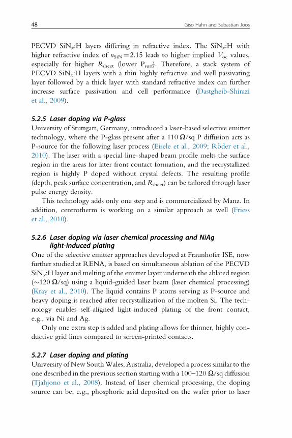
PECVD SiNx:H layers differing in refractive index. The SiNx:H with
higher refractive index of nSiN¼2.15 leads to higher implied Voc values,
especially for higher Rsheet (lower Psurf). Therefore, a stack system of
PECVD SiNx:H layers with a thin highly refractive and well passivating
layer followed by a thick layer with standard refractive index can further
increase surface passivation and cell performance (Dastgheib-Shirazi
et al., 2009).
5.2.5 Laser doping via P-glassUniversity of Stuttgart, Germany, introduced a laser-based selective emitter
technology, where the P-glass present after a 110 Ω/sq P diffusion acts as
P-source for the following laser process (Eisele et al., 2009; R€oder et al.,2010). The laser with a special line-shaped beam profile melts the surface
region in the areas for later front contact formation, and the recrystallized
region is highly P doped without crystal defects. The resulting profile
(depth, peak surface concentration, and Rsheet) can be tailored through laser
pulse energy density.
This technology adds only one step and is commercialized by Manz. In
addition, centrotherm is working on a similar approach as well (Friess
et al., 2010).
5.2.6 Laser doping via laser chemical processing and NiAglight-induced plating
One of the selective emitter approaches developed at Fraunhofer ISE, now
further studied at RENA, is based on simultaneous ablation of the PECVD
SiNx:H layer and melting of the emitter layer underneath the ablated region
(�120 Ω/sq) using a liquid-guided laser beam (laser chemical processing)
(Kray et al., 2010). The liquid contains P atoms serving as P-source and
heavy doping is reached after recrystallization of the molten Si. The tech-
nology enables self-aligned light-induced plating of the front contact,
e.g., via Ni and Ag.
Only one extra step is added and plating allows for thinner, highly con-
ductive grid lines compared to screen-printed contacts.
5.2.7 Laser doping and platingUniversity of New SouthWales, Australia, developed a process similar to the
one described in the previous section starting with a 100–120 Ω/sq diffusion(Tjahjono et al., 2008). Instead of laser chemical processing, the doping
source can be, e.g., phosphoric acid deposited on the wafer prior to laser
48 Giso Hahn and Sebastian Joos

doping. It allows for self-aligned plating of the front contacts as well. Both
processes insert extra steps after firing of the Al-BSF, which can therefore be
optimized independently of the front contact. In this approach, a plated Ni/
Cu/Ag front contact stack is used.
Two extra steps are added, and the approach allows for thinner,
highly conductive grid lines as well. Roth & Rau are working on
commercialization.
5.2.8 Effect of encapsulation on blue responseSelective emitters show an increase in j–V parameters on solar cell level as
demonstrated above, but the enhanced performance has to occur on module
level after encapsulation under glass as well. As part of the gain in short wave-
length IQE might be lost due to absorption after encapsulation, experiments
have been carried out to investigate this effect.
In Fig. 1.24, transmission curves for pure module glass and EVA under
module glass are shown. It can clearly be seen that the EVA starts to limit
the transmission at around 380 nm, whereas the module glass transmits sig-
nificantly shorter wavelengths. This negative effect of EVA concerning
transmittance could be overcome by the use of alternative materials like sil-
icones (Ketola et al., 2008; Ohl and Hahn, 2008). As shown in Fig. 1.24, the
transmission of silicone under module glass is almost identical to the curve of
the module glass alone. Therefore, encapsulation of solar cells under glass
using silicones would provide a better use of the short wavelength photons.
400 600 800 1000 12000
20
40
60
80
100
Module glassEVA on module glassSilicone on module glass
Tra
nsm
issi
on (
%)
l (nm)
Figure 1.24 Transmission of module glass, EVA under module glass, and silicone undermodule glass. Whereas EVA limits transmittance below 380 nm, silicone has a bettertransmission of short wavelength photons. Data from Ohl and Hahn (2008).
49State-of-the-Art Industrial Crystalline Silicon Solar Cells
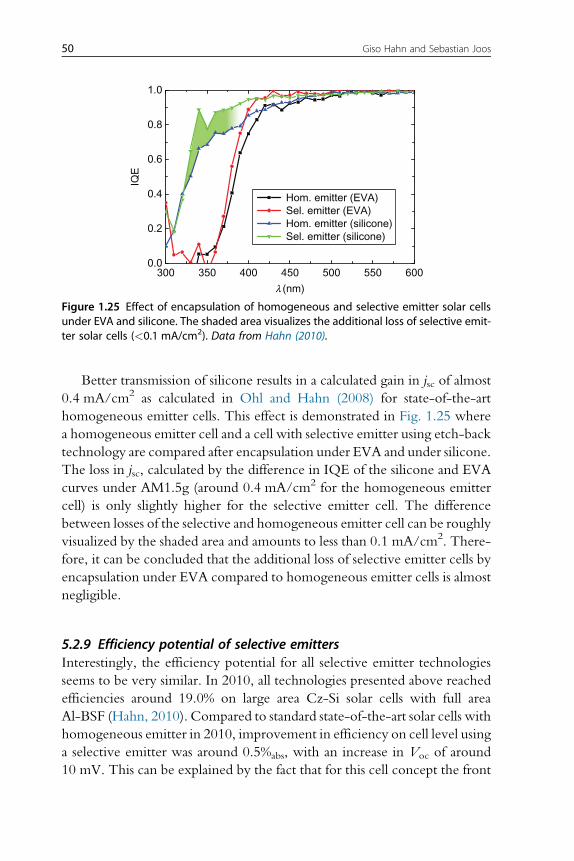
Better transmission of silicone results in a calculated gain in jsc of almost
0.4 mA/cm2 as calculated in Ohl and Hahn (2008) for state-of-the-art
homogeneous emitter cells. This effect is demonstrated in Fig. 1.25 where
a homogeneous emitter cell and a cell with selective emitter using etch-back
technology are compared after encapsulation under EVA and under silicone.
The loss in jsc, calculated by the difference in IQE of the silicone and EVA
curves under AM1.5g (around 0.4 mA/cm2 for the homogeneous emitter
cell) is only slightly higher for the selective emitter cell. The difference
between losses of the selective and homogeneous emitter cell can be roughly
visualized by the shaded area and amounts to less than 0.1 mA/cm2. There-
fore, it can be concluded that the additional loss of selective emitter cells by
encapsulation under EVA compared to homogeneous emitter cells is almost
negligible.
5.2.9 Efficiency potential of selective emittersInterestingly, the efficiency potential for all selective emitter technologies
seems to be very similar. In 2010, all technologies presented above reached
efficiencies around 19.0% on large area Cz-Si solar cells with full area
Al-BSF (Hahn, 2010). Compared to standard state-of-the-art solar cells with
homogeneous emitter in 2010, improvement in efficiency on cell level using
a selective emitter was around 0.5%abs, with an increase in Voc of around
10 mV. This can be explained by the fact that for this cell concept the front
300 350 400 450 500 550 6000.0
0.2
0.4
0.6
0.8
1.0
Hom. emitter (EVA)Sel. emitter (EVA)Hom. emitter (silicone)Sel. emitter (silicone)
IQE
l (nm)
Figure 1.25 Effect of encapsulation of homogeneous and selective emitter solar cellsunder EVA and silicone. The shaded area visualizes the additional loss of selective emit-ter solar cells (<0.1 mA/cm2). Data from Hahn (2010).
50 Giso Hahn and Sebastian Joos
side is not the limiting region anymore. The efficiency of these cells is mainly
limited by the recombination at the rear side (full area Al-BSF).
Since 2010 a lot of effort was put into development of new Ag pastes,
allowing for higherRsheet to be contacted. Therefore, part of the motivation
for application of selective emitter structures is weakened. On the other
hand, some benefits of selected selective emitter technologies, like broad fir-
ing windows and better electrical yield due to deeper emitters remain and are
still of importance. In addition, the formation of selective emitters might be
of higher interest again when the solar cell design on the rear side is changed
toward local contacts, decreasing recombination at the rear and putting
emphasis again toward the front side quality.
6. INDUSTRIAL PERC-TYPE SOLAR CELLS
In addition to the improvements of the standard process discussed in
the last section, a lot of effort is spent to implement more radical changes in
cell architecture into the industrial mass production cell process. After opti-
mization of the emitter quality described in the last section, the full area
Al-BSF is now the main reason for limiting efficiency of cells fabricated from
high quality Si material to values below 20% in mass production. Therefore,
different concepts based on locally contacted rear sides in combination with
a dielectric passivation of the largest part of the rear side area have been
developed. Some concepts available for this purpose have been introduced
first on lab-type solar cell processes and are the passivated emitter and rear
cell (PERC, Blakers et al., 1989), the passivated emitter and rear locally dif-
fused (PERL, Wang et al., 1990), and the passivated emitter rear totally dif-
fused (PERT, Zhao et al., 1999) concepts (Fig. 1.26). All of these concepts
have in common that most of the rear side area is dielectrically passivated (by
thermally grown SiO2 in the original lab-type processes) and only local con-
tacts are applied (mainly by photolithography for lab-type processes). The
differences between the mentioned concepts are
• PERC: metal contact directly on Si with moderate base doping
• PERL: locally diffused highly doped area (BSF) in the contacted
areas only
• PERT: rear side totally diffused (full area BSF) with local contacts.
For p-type solar cell concepts, the BSF (locally for PERL or full area for
PERT) was first applied via B diffusion. For all concepts, recombination
of charge carriers at the rear is drastically reduced compared to the standard
process described in the sections above. Efficiencies of up to 25% could be
51State-of-the-Art Industrial Crystalline Silicon Solar Cells

reached on small area cells (Zhao et al., 1999), demonstrating the efficiency
potential. The drawback of these cell concepts was for a long time that the
cell process was very complex, adding many extra steps and therefore calling
its industrial realization into question. In recent years, a lot of effort was put
into development of alternative processing steps allowing for an industrial
realization of a passivated rear side solar cell concept. In the following, pro-
gress toward implementation of these cell concepts into industrial produc-
tion will be reported.
6.1. Dielectric rear side passivationFor lab-type solar cells, rear side passivation was originally realized by long
high temperature thermal oxidation steps to grow SiO2 layers in the range of
100 nm thickness at temperatures above 1000 �C. This type of processing isthought not to be applicable in industrial mass production for reasons of
throughput and material issues.23 Therefore, alternative passivation schemes
AlAl2O3/SiNx:H
SiNx:H
p-Si
Ag
n+n
AlAl2O3/SiNx:H
SiNx:H
p-Si
Ag
n+
p++
n
AlAl2O3/SiNx:H
SiNx:H
p-Si
Ag
n+
p++
n
Figure 1.26 Schematics of Al2O3/SiNx:H passivated rear side concepts with selectiveemitter: PERC (top), PERL (center), and PERT (bottom).
23 Many c-Si materials cannot withstand temperatures above 950 �C because of the underlying defect
structure. This is especially important for mc-Si material.
52 Giso Hahn and Sebastian Joos

had to be developed for industrial solar cell processing. Surface passivation of
p-type surfaces can either be reached by chemical passivation, or by field
effect passivation with layers having negative fixed charges close to the
dielectric/silicon interface. In this case, the negative fixed charges attract
holes (majority carriers) and repel electrons (minority carriers), reducing
the recombination probability. In principle, also positive fixed charges at
the interface as present, e.g., in SiNx:H layers can reduce surface recombi-
nation for p-type silicon, provided that the charge is high enough to bring
the semiconductor in the regime of inversion (then attracted electrons show
a higher density close to the surface than holes, again decreasing recombi-
nation). But it could be shown that such a concept based on an inversion
layer is not very well suited for solar cell production (Agostinelli et al.,
2005; Finck von Finckenstein et al., 2000), as there is a high probability that
the inversion layer will be shunted duringmetallization (Dauwe et al., 2002).
6.1.1 Al2O3 layersIt is known for quite some time that Al2O3 layers can offer a good surface
passivation effect for PV application (Hezel and Jaeger, 1989; Jager and
Hezel, 1985). The reason is the existence of a high amount of fixed negative
charges at the dielectric/silicon interface, allowing for excellent passivation
of p-type silicon surfaces (Agostinelli et al., 2006). The field effect passiv-
ation of the Al2O3 by negative fixed charges has to be activated by temper-
atures of around 400 �C or higher (Hoex et al., 2006). Possible ways for
deposition of Al2O3 layers are, e.g., atomic layer deposition (ALD;
Agostinelli et al., 2006; Hoex et al., 2006), PECVD (Miyajima et al.,
2008), or APCVD (Black and McIntosh, 2012). First large area solar cells
with Al2O3 rear side passivation have been reported in 2009 (Vermang
et al., 2009), but the layers showed poor stability during the high temper-
ature firing step needed for screen-printing contact formation.
6.1.2 Al2O3/SiNx:H stacksThe refractive index of Al2O3 is in the range of 1.6–1.7 (Hoex et al., 2006)
and therefore not optimal for optics. A possible way to improve optics is the
application of a stacked layer system with a thin layer of Al2O3 and a thicker
layer of PECVD SiNx:H with refractive index of around 2.0. This allows for
better optics as well as a sufficiently good firing stability (Dingemans et al.,
2009). Positive fixed charges of the SiNx:H layer have no negative effect on
the passivation quality of the Al2O3, as long as the Al2O3 layer exceeds a
minimum thickness of around 5 nm (Richter, 2014; Schmidt et al., 2010).
53State-of-the-Art Industrial Crystalline Silicon Solar Cells

First large area solar cells with Al2O3/SiNx:H rear side passivation have
been published in 2010 (Lauermann et al., 2010), and reasonably good sur-
face passivation after the firing step could be demonstrated.
6.1.3 SiO2/SiNx:H stacksAn alternative to Al2O3/SiNx:H stack systems is the use of SiO2/SiNx:H sta-
cks. Here, the SiO2 layer can, e.g., be grown by thermal oxidation or by
PECVD, the latter allowing that both layers can be deposited in a single
PECVD run. The SiO2 layer can shield the positive fixed charges of the
SiNx:H and provides a good chemical passivation, subject to the condition
that a sufficient amount of H is present at the SiO2/Si interface. Therefore,
SiO2/SiNx:H stack systems usually gain in surface passivation after the firing
step, whereas the passivation quality of Al2O3/SiNx:H stacks is reduced after
firing.24 Nevertheless, the absolute overall passivation quality of Al2O3/SiNx:
H stacks after firing is usually still higher than for SiO2/SiNx:H stacks.
6.2. Formation of local rear contactsFor local rear contact formation, the formed dielectric layer has to be opened
locally. Different approaches have been developed for this purpose:
• Local firing of the metal through the dielectric layer
• Local application of an etching medium followed by local etching of the
dielectric layer
• Local ablation of the dielectric layer, e.g., by laser.
6.2.1 Laser fired contactsAn elegant way for realizing a local rear side metallization scheme is the for-
mation of laser fired contacts (LFC; Schneiderl€ochner et al., 2002). Here, the
full area Al is deposited on the not yet opened dielectric layer. Afterward, a
laser pulse is applied and locally melts the Al and removes the dielectric. Dur-
ing cooling down, a contact between Al and c-Si is formed. This approach
was first developed for evaporated or sputtered layers of Al, and it could be
shown that during cooling down a thin Al-BSF is formed at least in the cen-
ter of a LFC (Glunz et al., 2003). This approach could also be transferred to
large area cells with screen-printed Al layers, with the LFC formation
applied after the firing step (Hofmann et al., 2008).
24 Compared to layers where the passivation was activated by an annealing step at around 400 �C.
54 Giso Hahn and Sebastian Joos

6.2.2 Etching pasteA medium able to etch through the dielectric layer can be applied locally to
the rear side of the wafer. This could, e.g., be realized via inkjet or screen-
printing of a paste containing phosphoric acid as etching medium (Bahr
et al., 2007). Normally, a thermal treatment is needed after application of
the etching paste to activate the chemical reaction, but the advantage is that
the c-Si underneath the dielectric layer is not damaged.
6.2.3 Laser ablationAnother approach is local ablation of the dielectric layer by using a short laser
pulse. Here, the aim is to remove the dielectric layer locally, with minimal
damage of the c-Si underneath. As the photon energy of the laser pulse
should be absorbed mainly in the dielectric layer, picosecond (ps) laser pulses
with wavelengths of 532 and 355 nm show very good results on planar sur-
faces (Engelhart et al., 2007; Hermann et al., 2010). High photon energy and
density result in most of the pulse energy being absorbed in the dielectric
layer, heating it up and evaporating it immediately. The short pulse length
assures that the thermal heat wave does not penetrate deep into the c-Si
underneath, restricting damage due to, e.g., thermal stresses to surface near
regions.
After local opening via etching or laser ablation, the Al paste is screen-
printed on the rear. During firing in a belt furnace, the Al paste without glass
frit does not etch through the dielectric, but forms only a local contact in the
areas previously opened.
6.2.4 Contact patterns and void formationWhile the LFC approach uses points as contact geometry, for the laser abla-
tion approach a line-shaped contact pattern is advantageous (Lauermann
et al., 2011). This can be understood considering the different formation
mechanisms of the local contacts. For LFC, during the very short laser pulse
no significant diffusion of Si into the Al layer can occur. This situation
changes when the contact is formed during the firing step in a belt furnace.
Here, the situation is similar to the standard full area BSF formation. Above
the eutectic temperature of Al/Si, Si is dissolved into the molten Al. As this
dissolution can only occur locally in the opened areas, the amount of Si dis-
solved into the Al depends on the geometry of the opening (Urrejola et al.,
2011). Depending on the temperature–time profile during firing, different
amounts of Si can diffuse into the Al layer, saturating the molten Al in some
areas, while others further away from the opening show lower Si
55State-of-the-Art Industrial Crystalline Silicon Solar Cells
concentrations below the values predicted by the Al/Si phase diagram
(Urrejola et al., 2010). During cooling down after firing, the BSF starts to
form when Si is repelled from the Al/Si melt, again according to the phase
diagram. For doing so, Si has to diffuse back to the local openings in the
dielectric layer. Depending on the amount of Si dissolved, BSF formation
might start at lower temperatures compared to the case of a full area BSF.
For a detailed model of local BSF formation using laser ablation see
Lauermann et al. (2013).
To reduce the effect of Si being dissolved into Al only to values below
the values according to the phase diagram at peak temperature, Si can be
added to the Al paste, reducing this unwanted effect, and improving BSF
formation (Rauer et al., 2011).
It is often observed that after application of local Al rear contacts voids in
the c-Si are formed in the opened areas (Meemongkolkiat et al., 2006). This
observation is often explained by the Kirkendall effect (Kirkendall, 1942).
These voids can be visualized by cross sectionmicroscopy or in a nondestruc-
tive way, e.g., by scanning acoustic microscopy (Dressler et al., 2012). Not
all voids have a direct negative influence on cell parameters. If a BSF is
formed and is in contact with the Al layer, the void does no harm, whereas
on the other hand a missing BSF is responsible for increased surface recom-
bination, and a noncontacted BSF causes increased Rs.
See also Riegel et al. (2012) for a review of screen-printing metallization
on p-type Si.
6.2.5 Interconnection issuesThe designs for local Al contact formation described above all result in
reduced recombination losses at the rear side. But for module interconnec-
tion ribbons have to be soldered to both rear and front contacts. On the rear
there are no Ag pads as in the case of the standard full Al-BSF cells, and as Al
paste is not solderable alternatives have to be found. One of them is the
deposition of Sn stripes on the rear using ultrasonic soldering (also called
tin pad; von Campe et al., 2012). On these pads interconnection ribbons
can be soldered.
Finally, it has to be mentioned that the cell structure with passivated rear
side and locally alloyed Al contact is often referred to as PERC or industrial
PERC structure. This might be somewhat misleading, as in the original
publications of the PERC solar cell structure, the metal is directly contacting
the base doping, without a highly doped p+ layer in between (Blakers et al.,
1989). The structures described above would therefore more precisely fall in
56 Giso Hahn and Sebastian Joos

the category of PERL cells, with the difference that the p+ areas below the
local metal contacts are not formed by (B) diffusion, but by (Al/B) alloying.
Nevertheless, the term PERC structure is used more frequently.
6.3. Boron–oxygen related degradationWith the front side improved using an optimized homogeneous emitter or a
selective emitter structure and recombination at the rear side reduced by
applying a passivation layer and only local contacts, τb sets the limit of effi-
ciency. For mc-Si, the underlying defect structure (dislocations, grain
boundaries, impurities, like, e.g., transition metals) can be identified as
source for τb limitation. For higher quality Cz-Si, the formation of
boron–oxygen (B–O) related defects plays a crucial role and is known for
a long time (Fischer and Pschunder, 1973). These defects can form at room
temperature in the presence of excess charge carriers, reducing τb signifi-
cantly (Bothe et al., 2003; Weizer et al., 1979). When the solar cell is illu-
minated during operation, B–O related defects formwithin the first hours of
operation of a solar module. The amount of defects formed scales linearly
with substitutional boron concentration Bs (Glunz et al., 2001; Schmidt
and Cuevas, 1999), and quadratically with interstitial O concentration Oi
(Rein et al., 2003; Schmidt and Bothe, 2004). A fundamental lifetime limit
in dependence of Bs and Oi could be found for the degraded state after for-
mation of the B–O related defects (Bothe et al., 2005), restricting τb to
τb ¼ 7:6751045Bs�0:824Oi
�1:748: (1.39)
The recombination active complexes become instable at temperatures
exceeding 140 �C in an anneal step in the dark, therefore the defect is called
metastable (Rein et al., 2001). The behavior of the metastable B–O related
defect can be understood by a conversion of two possible states into each
other (annealed state and degraded state). In the annealed state, the complex
shows negligible recombination activity, but in the presence of charge car-
riers it is transformed into the degraded state again, with a thermally activated
reaction rate.
6.3.1 Strategies to deal with B–O related degradationFor most standard solar cell concepts, bulk resistivities of around 0.5–1 Ω cm
allow for the highest conversion efficiency. With Oi in standard Cz material
in the range of 1018 per cm3 and Bs of 1016 per cm3, bulk lifetime calculated
according to Eq. (1.39) results in only 9 μs for the degraded state. Therefore,
57State-of-the-Art Industrial Crystalline Silicon Solar Cells

strategies to prevent this severe degradation effect have to be considered.
One possibility is to avoid B as a dopant and the usage of another p-type
dopant like Ga (Glunz et al., 2001). Unfortunately, Ga has a segregation
coefficient much smaller than B, resulting in inhomogeneous doping and
therefore variations in bulk resistivity with ingot height (Trumbore, 1960).
Another possibility is to reduce formation of Oi during crystallization.
This can, e.g., be achieved by applying an external magnetic field (Mosel
et al., 2012). Very good results have been achieved (Glunz et al., 2001),
but extra costs have to be considered.
The easiest way is to use a lower Bs, as B is deliberately added to the melt.
This reduces the efficiency potential in the annealed state, but allows for
higher efficiencies in the degraded state after illumination. This approach
is followed in industry today, as 2–5 Ω cm B-doped Cz material is
normally used.
6.3.2 Regeneration of B–O related defectsIn 2006, it was discovered that the degraded state of the B–O related defect
can be transformed into another state, which is stable under illumination and
shows negligible recombination activity (Herguth et al., 2006a,b). This
regenerated state can be reached by slightly elevated temperatures and the
presence of excess charge carriers25 (Herguth et al., 2008). This new state
of the B–O related defect is stable under illumination and room temperature,
and therefore allows for high and stable efficiencies at operating conditions
of a solar cell under illumination. The three states of the defect (annealed,
degraded, and regenerated) are depicted in Fig. 1.27. For higher tempera-
tures >200 �C, the regenerated state can become unstable, and the B–O
related defect is in the annealed state, from where it can degrade again in
the presence of excess charge carriers at lower temperatures. It is still unclear
if the reaction path is directly from state C to state A (destabilization in
Fig. 1.27) or via state B. A model based on reaction constants has been pro-
posed to explain and predict the observed kinetics of the defect in detail
(Herguth and Hahn, 2010).
It could be shown that the presence of H might have an influence for the
regeneration reaction to occur (Munzer, 2009). This could be verified, as
test samples with unfired SiNx:H layers did not show a regeneration effect,
while fired samples did (Wilking et al., 2013a). Also layers inserted between
c-Si and SiNx:H acting as a barrier for H slow down the regeneration
25 Excess charge carriers can be generated via illumination or biasing of the solar cell.
58 Giso Hahn and Sebastian Joos

process, indicating that H in sufficient concentration in the c-Si bulk is a
prerequisite for the regeneration process to work. The firing process plays
a crucial role in adjusting the concentration of H in the final solar cell,
strongly influencing the regeneration kinetics (Wilking et al., 2013b).
Choosing the right firing parameters and regeneration conditions, the
regeneration process can be carried out within seconds (Wilking et al.,
2014), opening a path toward stable efficiencies for p-type B-doped material
with high Oi and bulk resistivities in the range of 1 Ω cm.
6.4. State-of-the-art industrial PERC solar cellsEfficiencies of 20.2% have been demonstrated on large area p-type boron
doped Cz-Si in 2011 using both the LFC technology (Engelhart et al.,
2011) as well as laser ablation for local opening of the dielectric and use
of an etched-back selective emitter (Gassenbauer et al., 2013). Optimiza-
tions led to efficiencies of up to 21.0% for the laser ablation approach in
2013 (Metz et al., 2014; Ramspeck et al., 2012). Applying the regeneration
process, these high efficiencies are stable under illumination.
The efficiencies reported here have been reached with screen-printed
metallization on the front and rear side. Even higher efficiencies of up to
21.3% are possible when plating approaches are used (Metz et al., 2014).
For some of these cells described above, a thin thermal oxide layer is placed
Destabilization
Regeneration
Redegradation
AnnealDegradation
State A“annealed”(inactive)
State C“regenerated”
(inactive)
State B“degraded”
(active)
Figure 1.27 Three state model of the B–O related defect. States A and C are recombi-nation inactive, but only state C is stable under illumination (after Herguth et al., 2006b).
59State-of-the-Art Industrial Crystalline Silicon Solar Cells
between the emitter and the SiNx:H ARC, improving surface passivation.
In addition, optimized emitter structures including an etch-back process are
used (Metz et al., 2014).
Interestingly, the described industrial PERC processes might be easier to
apply to mc-Si instead of Cz-Si. This seems to be counterintuitive, as Cz-Si
might contain fewer defects than mc-Si, resulting in higher material quality,
and therefore the efficiency potential of Cz-Si should be more sensitive for a
lower rear surface recombination. But without application of the regener-
ation process to deactivate the B–O related defects, Cz-Si of higher base
resistivity is used to avoid strong degradation under illumination (see above).
Therefore, the p+/p interface formed between the full area Al-BSF and the
c-Si forms a steeper high/low junction in the case of high bulk resistivity,
lowering seff for Cz-Si to values below the ones for 1 Ω cm mc-Si (see
Eq. 1.36). This means that it is more difficult for Cz-Si of higher bulk resis-
tivity to achieve lower rear surface recombination by dielectric passivation as
compared to full area Al-BSF processing than for mc-Si of lower bulk
resistivity.
7. SUMMARY AND OUTLOOK
Since 2000 the yearly shipment of PV cells and modules increased by a
factor of 100, indicating the tremendous progress that could be achieved.
Interestingly though, the standard industrial solar cell fabrication process
did not change too much over the past one to two decades. B-doped
p-type wafer based Si is still the material of choice, and screen-printing of
metal pastes is used for metallization.
Most of the processing steps have been optimized. Examples are the
development of high Rsheet emitters, resulting in lower j0e. This was only
possible by the parallel development of new Ag pastes, allowing the con-
tacting of these emitter structures without increased contact resistivity.
Advances have also been achieved in front side screen-printing, with typical
Ag finger width in the range of 60–80 μm. Other examples are optimized
front surface texture solutions and Al rear side pastes, co-doped with B.
But also more disruptive changes have been implemented into the stan-
dard cell fabrication process. After introduction of PECVD SiNx:H as ARC
and surface passivation layer, solar cell efficiencies could be significantly
increased, especially for defect-rich mc-Si solar cells. In addition, with
the introduction of acidic surface textures mc-Si now shows a significantly
higher market share as compared to Cz-Si, due to lower wafer fabrication
60 Giso Hahn and Sebastian Joos

costs. Selective emitter structures have been introduced into mass produc-
tion, especially when they fit into the layout of the cell process.26
Altogether, an evolutionary process development was chosen based on
the very robust industrial standard process to minimize the risk of failure.
Especially in times of very dynamic market growth this approach is favored,
as existing solar cell lines can be duplicated adding only slight changes in
equipment or solar cell design. For the introduction of passivated rear sides
with local rear contacts (PERC-type structures), the cell process has to be
adapted more drastically, as several processing steps have to be added or
changed. It remains to be seen if this technology will be the next step to
be introduced into the standard process, or if it will be a parallel approach.
Last but not least, there are many other cell designs under development at
the moment, all introducing more disruptive changes compared to the stan-
dard process. Some of them are already in industrial mass production (or
close to), but most of them are currently used by only a handful of compa-
nies. Therefore, these technologies have not been part of this chapter.
Examples are
• n-type Si wafers
• Rear contacted solar cells (van Kerschaver and Beaucarne, 2006)
• Heterojunction emitter technology (Ballif et al., 2014).
The reason why these very interesting technologies are under investigation
is the fact that they currently show higher efficiency potential. Whether this
can also result in a more cost-effective PV electricity generation compared to
the standard process route still remains to be seen, as many other factors apart
from efficiency play a crucial role (yield, stability of the process, location of
PV installation). It is hard to predict which process route and cell design will
be the most cost-effective in the future. But it can be assumed that within the
next decades there will be several c-Si technologies followed in industrial
production in parallel, with many of them being commercially successful
in the mass market or for niche applications.
Today solar cells and modules are mainly optimized according to STC
(25 �C, 1000 W/m2) as this measurement is fast enough to be included in
a production line and states a good measure for high irradiance environ-
ments. The field conditions for solar cells, however, may be quite different.
Here, higher module temperatures, lower irradiations, and stray light
26 An example is the etch-back selective emitter process, if edge isolation is carried out wet chemically
anyway.
61State-of-the-Art Industrial Crystalline Silicon Solar Cells

conditions are often found. Therefore, an additional optimization of PV
solar systems in terms of generated electricity under these conditions is
desirable.
ACKNOWLEDGMENTSWe like to thank H. Haverkamp and A. Zuschlag for proof-reading and the German
government for continuous funding of projects over the past decades.
REFERENCESAberle, A.G., 1999. Crystalline Silicon Solar Cells—Advanced Surface Passivation and Anal-
ysis. Centre for Photovoltaic Engineering, University of New South Wales, Sydney.Agostinelli, G., Choulat, P., Dekkers, H., De Wolf, S., 2005. Screen printed large area
crystalline silicon solar cells on thin substrates. In: Proceedings of the 20th EU PVSEC,Barcelona, pp. 647–650.
Agostinelli, G., Delabie, A., Vitanov, P., Alexieva, Z., Dekkers, H.F.W., De Wolf, S.,Beaucarne, G., 2006. Very low surface recombination velocities on p-type silicon waferspassivated with a dielectric with fixed negative charge. Sol. Energ. Mat. Sol. C90, 3438–3443.
Antoniadis, H., Jiang, F., Shan, W., Liu, Y., 2010. All screen printed mass produced siliconink selective emitter solar cells. In: Proceedings of the 35th IEEE PVSC, Honolulu,pp. 1193–1196.
Bahr, M., Kim, S., Sridharan, S., Khadilkar, C., Shaikh, A., K€ohler, I., Reichardt, M.,Kumar, M., 2007. A new approach for the front side metallization of industrial type sil-icon solar cells using a structurization by etching. In: Proceedings of the 22nd EUPVSEC, Milano, pp. 1015–1019.
Ballif, C., Huljic, D.M., Hessler-Wysser, A.,Willeke, G., 2002. Nature of the Ag-Si interfacein screen-printed contacts: a detailed transmission electron microscopy study of cross-sectional structures. In: Proceedings of the 29th IEEE PVSC, New Orleans,pp. 360–363.
Ballif, C., Huljic, D.M., Willeke, G., Hessler-Wysser, A., 2003. Silver thick-film contacts onhighly doped n-type silicon emitters: structural and electronic properties of the interface.Appl. Phys. Lett. 82 (12), 1878–1880.
Ballif, C., Descoeudres, A., Holman, Z., De Wolf, S., 2014. Amorphous silicon/crystallinesilicon heterojunction solar cells. In: Willeke, G., Weber, E. (Eds.), Semiconductors andSemimetals, Advances in Photovoltaics: Part 3. Elsevier, Amsterdam.
Basu, P.K., Sarangi, D., Shetty, K.D., Boreland, M.B., 2013. Liquid silicate additive for alka-line texturing of mono-Si wafers to improve process bath lifetime and reduce IPA con-sumption. Sol. Energ. Mat. Sol. C 113, 37–43.
Bentzen, A., Holt, A., Christensen, J.S., Svensson, B.G., 2006a. High concentrationin-diffusion of phosphorus in Si from a spray-on source. J. Appl. Phys. 99, 064502.
Bentzen, A., Christensen, J.S., Svensson, B.G., Holt, A., 2006b. Understanding phosphorusemitter diffusion in silicon solar cell processing. In: Proceedings of the 21st EU PVSEC,Dresden, pp. 1388–1391.
Beutel, M., Lewis, A., Prondzinski, M., Selbmann, F., Richter, P., Bamberg, F.,Raschtschepkin, P., Krause, A., Koch, C., Hentsche, M., Stegemann, K.-H.,Schneiderl€ochner, E., Neuhaus, H., 2014. Fine line metallization by coextrusion tech-nology for next generation solar cells. Sol. Energ. Mater. Sol. Cell 131, 64–71.
Black, L.E., McIntosh, K.R., 2012. Surface passivation of c-Si by atmospheric pressurechemical vapour deposition of Al2O3. Appl. Phys. Lett. 100, 202107.
62 Giso Hahn and Sebastian Joos

Blakers, A.W., Wang, A., Milne, A.M., Zhao, J., Green, M.A., 1989. 22.8% efficient siliconsolar cell. Appl. Phys. Lett. 55 (13), 1363–1365.
Book, F., 2014. Hocheffiziente Industrie-Solarzellen mit selektiver Oberflachendotierung.Dissertation, University of Konstanz.
Book, F., Dastgheib-Shirazi, A., Raabe, B., Haverkamp, H., Hahn, G., Grabitz, P., 2009.Detailed analysis of high sheet resistance emitters for selectively doped silicon solar cells.In: Proceedings of the 24th EU PVSEC, Hamburg, pp. 1719–1722.
Book, F., Wiedenmann, T., Dastgheib-Shirazi, A., Raabe, B., Hahn, G., 2010. Largearea n-type silicon solar cells with selective front surface field and screen printedaluminum-alloyed rear emitter. In: Proceedings of the 25th EU PVSEC, Valencia,pp. 1465–1468.
Book, F., Wiedenmann, T., Schubert, G., Plagwitz, H., Hahn, G., 2011. Influence of thefront surface passivation quality on large area n-type silicon solar cells with Al-alloyedemitter. Energy Procedia 8, 487–492.
Bothe, K., Hezel, R., Schmidt, J., 2003. Recombination-enhanced formation of themetastable boron-oxygen complex in crystalline silicon. Appl. Phys. Lett. 83,1125–1127.
Bothe, K., Sinton, R., Schmidt, J., 2005. Fundamental boron-oxygen-related carrier lifetimelimit in mono- and multi-crystalline silicon. Prog. Photovolt. Res. Appl. 13, 287–296.
Braun, S., 2014. Simulation, Analyse und Herstellung von kristallinen Si-Solarzellen mitMultibusbar-Verschaltung. Dissertation, University of Konstanz.
Braun, S.,Micard, G., Hahn, G., 2012. Solar cell improvement by using amulti busbar designas front electrode. Energy Procedia 27, 227–233.
Braun, S., Hahn, G., Nissler, R., P€onisch, C., Habermann, D., 2013a. Multi-busbar solarcells and modules: high efficiencies and low silver consumption. Energy Procedia38, 334–339.
Braun, S., Nissler, R., Habermann, D., Hahn, G., 2013b. Highly efficient multi-busbar solarcells with Ag nano-particle front side metallization. In: Proceedings of the 28th EUPVSEC, Paris, pp. 1148–1151.
Braun, S., Nissler, R., Ebert, C., Habermann, D., Hahn, G., 2014. High efficiency multi-busbar solar cells and modules. IEEE J. Photovolt. 4 (1), 148–153.
Buchwald, R., Wurzner, S., Fr€ohlich, K., Winstanley, S., Lehmann, T., Sunder, K.,M€oller, H.J., 2013. Analysis of the sub-surface damage of mc- and Cz wafers sawn withdiamond-plated wire. In: Proceedings of the 28th EU PVSEC, Paris, pp. 1502–1506.
Buonassisi, T., Istratov, A.A., Pickett, M.D., Heuer, M., Kalejs, J.P., Hahn, G., Marcus, M.A.,Lai, B., Cai, Z.,Heald, S.M.,Ciszek, T.F., Clark,R.F.,Cunningham,D.W.,Gabor, A.M.,Jonczyk, R., Narayanan, S., Sauar, E., Weber, E.R., 2006. Chemical natures anddistributions of metal impurities in multi-crystalline silicon materials. Prog. Photovolt.Res. Appl. 14, 513–531.
Cabrera, E., Olibet, S., Glatz-Reichenbach, J., Kopecek, R., Reinke, D., Schubert, G.,2011. Experimental evidence of direct contact formation for the current transport in sil-ver thick film metallized silicon emitters. J. Appl. Phys. 110, 114511.
Cabrera, E., Olibet, S., Rudolph, D., Vullum, P.E., Kopecek, R., Reinke, D., Herzog, C.,Schwaderer, D., Schubert, G., 2013. Impact of excess phosphorus doping and Si crys-talline defects on Ag crystallite nucleation and growth in silver screen-printed Si solarcells. Prog. Photovolt. Res. Appl, http://dx.doi.org/10.1002/pip.2440.
Carrol, A.F., 2013. Screen printed metal contacts to Si solar cells—formation and synergisticimprovements. In: Proceedings of the 39th IEEE PVSC, Tampa, pp. 3435–3440.
Ceccaroli, B., Pizzini, S., 2012. Processes. In: Pizzini, S. (Ed.), Advanced SiliconMaterials forPhotovoltaic Applications. Wiley, Chichester, pp. 21–78.
Chapin, D.M., Fuller, C.S., Pearson, G.L., 1954. A new silicon p–n junction photocell forconverting solar radiation into electrical power. J. Appl. Phys. 25 (5), 676.
63State-of-the-Art Industrial Crystalline Silicon Solar Cells

Coletti, G., Macdonald, D., Yang, D., 2012. Role of impurities in solar silicon. In: Pizzini, S.(Ed.), Advanced Silicon Materials for Photovoltaic Applications. Wiley, Chichester,pp. 79–125.
Cousins, P.J., Smith, D.D., Luan, H.-C., Manning, J., Dennis, T.D., Waldhauer, A.,Wilson, K.E., Harley, G., Mulligan, W.P., 2010. Generation 3: improved performanceat lower cost. In: Proceedings of the 35th IEEE PVSC, Honolulu, pp. 275–278.
Cube, C.E., Hanoka, J.I., 2005. Hydrogen passivation of multicrystalline silicon.In: Procceedings of the 31st IEEE PVSC, Lake Buena Vista, pp. 883–888.
Cuevas, A., Basore, P.A., Giroult-Matlakowski, G., Dubois, C., 1996. Surface recombina-tion velocity of highly doped n-type silicon. J. Appl. Phys. 80, 3370–3375.
Dastgheib-Shirazi, A., Book, F., Haverkamp, H., Raabe, B., Hahn, G., 2009. Investigationsof high refractive silicon nitride layers for etched back emitters: enhanced surface passiv-ation for selective emitter concept (SECT). In: Proceedings of the 24th EU PVSEC,Hamburg, pp. 1600–1604.
Dastgheib-Shirazi, A., Steyer, M., Micard, G., Wagner, H., Altermatt, P., Hahn, G., 2012.Effects of process conditions for the n+-emitter formation in crystalline silicon.In: Proceedings of the 38th IEEE PVSC, Austin, pp. 1584–1589.
Dastgheib-Shirazi, A., Micard, G., Wagner, H., Steyer, M., Altermatt, P.P., Hahn, G.,2013a. Towards an optimized emitter for screen-printed solar cells. In: Proceedings ofthe 39th IEEE PVSC, Tampa.
Dastgheib-Shirazi, A., Steyer, M., Micard, G., Wagner, H., Altermatt, P.P., Hahn, G.,2013b. Relationships between diffusion parameters and phosphorus precipitation duringthe POCl3 diffusion process. Energy Procedia 38, 254–262.
Dauwe, S., Mittelstadt, L., Metz, A., Hezel, R., 2002. Experimental evidence of parasiticshunting in silicon nitride rear surface passivated solar cells. Prog. Photovolt. Res. Appl.10 (4), 271–278.
Delahaye, F., L€ohmann, M., Bauer, M., Vilsmeier, G., Melnyk, I., Hauser, A., Gerhards, C.,Krause, M., Lust, S., Nußbaumer, H., Joos, W., 2004. Edge isolation: innovative inlinewet processing—ready for industrial production. In: Proceedings of the 19th EUPVSEC, Paris, pp. 416–418.
del Alamo, J., Eguren, J., Luque, A., 1981. Operating limits of Al-alloyed high-low junctionsfor BSF solar cells. Solid-State Electron. 24, 415–420.
deMoor, H.H.C., Hoornstra, J.,Weeber, A.W., Burgers, A.R., Sinke,W.C., 2012. Printinghigh and fine metal lines using stencils. In: Proceedings of the 14th EU PVSEC, Barce-lona, pp. 404–407.
Dingemans, G., Engelhart, P., Seguin, R., Einsele, F., Hoex, B., van de Sanden, M.C.M.,Kessels, W.M.M., 2009. Stability of Al2O3 and Al2O3/a-SiNx:H stacks for surface pas-sivation of crystalline silicon. J. Appl. Phys. 106, 114907.
Dold, P., 2014. Silicon crystallization and wafering. In: Willeke, G., Weber, E. (Eds.),Semiconductors and Semimetals, Advances in Photovoltaics, Part 3. Elsevier,Amsterdam.
Dressler, K., Dauwe, S., Droste, T., Rossa, J., Meidel, R., Schunemann, K., Ramspeck, K.,Gassenbauer, Y., Metz, A., 2012. Characterisation of rear local contacts including BSFformation using Raman and scanning acoustic microscopy. In: Proceedings of the 27thEU PVSEC, Frankfurt, pp. 755–758.
Duerinckx, F., Szlufcik, J., 2002. Defect passivation of industrial multicrystalline solar cellsbased on PECVD silicon nitride. Sol. Energ. Mat. Sol. C 72 (1–4), 231–246.
Einhaus, R., Vazsony, E., Szlufcik, J., Nijs, J., Mertens, R., 1997. Isotropic texturing of mul-ticrystalline silicon wafers with acidic texturing solutions. In: Proceedings of the 26thIEEE PVSC, Anaheim, pp. 167–170.
Eisele, S.J., R€oder, T.C., K€ohler, J.R., Werner, J.H., 2009. 18.9% efficient full area laserdoped silicon solar cell. Appl. Phys. Lett. 95, 133501.
64 Giso Hahn and Sebastian Joos
Emanuel, G., Schneiderl€ochner, E., Stollhof, J., Gentischer, J., Preu, R., Ludemann, R.,2001. High throughput laser isolation of crystalline silicon solar cells. In: Proceedingsof the 17th EU PVSEC, Munich, pp. 1578–1581.
Engelhart, P., Herman, S., Neubert, T., Plagwitz, H., Grischke, R., Meyer, R., Klug, U.,Schoonderbeek, A., Stute, U., Brendel, R., 2007. Laser ablation of SiO2 for locally con-tacted Si solar cells with ultra-short pulses. Prog. Photovolt. Res. Appl. 15, 521–527.
Engelhart, P.,Manger,D., Kl€oter, B., Hermann, S., Stekolnikov, A.A., Peters, S., Ploigt, H.-C.,Eifler, A., Klenke, C., Mohr, A., Zimmermann, G., Barkenfelt, B., Suva, K., Wendt, J.,Kaden, T., Rupp, S., Rychtarik, D., Fischer, M., Muller, J.W., Wawer, P., 2011. Q.ANTUM—Q-cells next generation high-power silicon cell & module concept.In: Proceedings of the 26th EU PVSEC, Hamburg, pp. 821–828.
Esturo-Breton, A., Binaie, F., Breselge, M., Friess, T., Geiger, M., Holbig, E., Isenberg, J.,Keller, S., Kuhn, T., Maier, J., Munzer, A., Schlosser, R., Schmid, A., Voyer, C.,Winter, P., Bayer, K., Krumberg, J., Henze, S., Melnyk, I., Schmidt, M.,Klingbeil, S., Walter, F., Kopecek, R., Peter, K., 2009. Crystalline silicon solar cells withselective emitter for industrial mass production. In: Proceedings of the 24th EU PVSEC,Hamburg, pp. 1068–1071.
Fabry, L., Hesse, K., 2012. Crystalline silicon feedstock preparation and analysis.In: Willeke, G., Weber, E. (Eds.), Semiconductors and Semimetals 87. In: Advancesin Photovoltaics, vol. 1. Elsevier, Amsterdam, pp. 185–261.
Fair, R.B., Tsai, J.C.C., 1977. A quantitative model for the diffusion of phosphorus in siliconand the emitter dip effect. J. Electrochem. Soc. 124 (7), 1107–1118.
Finck von Finckenstein, B.,Horst,H., Fath, P., Bucher, E., 2000.ThinmcSi low cost solar cellswith 15% efficiency. In: Proceedings of the 28th IEEE PVSC, Anchorage, pp. 198–200.
Fischer, B., 1994. Metallisation of silicon solar cells. Master thesis, Australian NationalUniversity, Canberra.
Fischer, H., Pschunder, W., 1973. Investigations on photon and thermal induced changesin silicon solar cells. In: Proceedings of the 10th IEEE PVSC, Palo Alto, pp. 404–411.
Friess, T., Esturo-Breton, A., Binaie, F., Breselge, M., Geiger, M., Isenberg, J., Keller, S.,Kuhn, T., Maier, J., Munzer, A., Schmid, A., Voyer, C., Winter, P.,Zimmermann, W., Bayer, K., Henze, S., Huls, S., Kastle, W., Krumberg, J.,Melnyk, I., Rasz, C., Schmidt, M., Walter, F., Kopecek, R., Peter, K.,Hildebrand, L., Muller, M., Fath, P., 2010. Selective emitter on crystalline Si solar cellsfor industrial high efficiency mass production. In: Proceedings of the 25th EU PVSEC,Valencia, pp. 2164–2167.
Gabor, A., 2012. Innovations in Crystalline Silicon PV 2013: Markets, Strategies and Leadersin Nine Technology Areas. Greentech Media, Boston, pp. 128–148.
Galiazzo, M., Furin, V., Cellere, G., Baccini, A., 2009. New technologies for improvementof metallization line. In: Proceedings of the 24th EU PVSEC, Hamburg, pp. 1502–1505.
Gassenbauer, Y., Ramspeck, K., Bethmann, B., Dressler, K., Moschner, J.D., Fiedler, M.,Brouwer, E., Dr€ossler, R., Lenck, N., Heyer, F., Feldhaus, M., Seidl, A., Muller, M.,Metz, A., 2013. Rear-surface passivation technology for crystalline silicon solar cells:a versatile process for mass production. IEEE J. Photovolt. 3 (1), 125–130.
Glunz, S.W., Rein, S., Warta, W., Knobloch, J., Wettling, W., 2001. Degradation of carrierlifetime in Cz silicon solar cells. Sol. Energ. Mat. Sol. C 65, 219–229.
Glunz, S.W., Grohe, A., Hermle, M., Schneiderl€ochner, E., Dicker, J., Preu, R.,Mackel, H., Macdonald, D., Cuevas, A., 2003. Analysis of laser-fired local back surfacefields. In: Proceedings of the 3rd WCPEC, Osaka, pp. 1332–1335.
Godlewski, M.P., Baraona, C.R., Brandhorst, H.W., 1973. Low-high junction theoryapplied to solar cells. In: Proceedings of the 10th IEEE PVSC, Palo Alto, pp. 40–49.
Goodrich, A., Hacke, P., Wang, Q., Sopori, B., Margolis, R., James, T.L., Woodhouse, M.,2013. A wafer-based monocrystalline silicon photovoltaics road map: utilizing known
65State-of-the-Art Industrial Crystalline Silicon Solar Cells
technology improvement opportunities for further reductions in manufacturing costs.Sol. Energ. Mat. Sol. C 114, 110–135.
Hahn, G., 2010. Status of selective emitter technology. In: Proceedings of the 25th EUPVSEC, Valencia, pp. 1091–1096.
Hahn, G., Sch€onecker, A., 2004. New crystalline silicon ribbon materials for photovoltaics.J. Phys. Condens. Matter 16, R1615–R1648.
Hahn, G., Sontag, D., Seren, S., Sch€onecker, A., Burgers, A.R., Ginige, R., Cherkaoui, K.,Karg, D., Charifi, H., 2004. Hydrogenation of multicrystalline silicon—the story con-tinues. In: Proceedings of the 19th EU PVSEC, Paris, pp. 427–430.
Hahn, G., Kas, M., Herzog, B., 2010. Hydrogenation in crystalline silicon materials for pho-tovoltaic application. Solid State Phenom. 156–158, 343–349.
Hall, R.N., 1952. Electron-hole recombination in germanium. Phys. Rev. 87 (2), 387.Hannebauer, H., Dullweber, T., Falcon, T., Chen, X., Brendel, R., 2013. Record low Ag
paste consumption of 67.7 mg with dual print. Energy Procedia 43, 66–71.Hanoka, J.I., 1989. An improved method of fabricating contacts for solar cells. U.S. Patent
1989/002241.Hanoka, J.I., Danielson, S.E., 1991. Method for forming contacts. U.S. Patent US5151377 A.Hauser, A., Hahn, G., Spiegel, M., Feist, H., Breitenstein, O., Rakotoniaina, J.P., Fath, P.,
Bucher, E., 2001. Comparison of different techniques for edge isolation. In: Proceedingsof the 17th EU PVSEC, Munich, pp. 1739–1742.
Hauser, A., Melnyk, I., Fath, P., Narayanan, S., Roberts, S., Bruton, T.M., 2003.A simplified process for isotropic texturing of mc-Si. In: Proceedings of the 3rdWCPEC, Osaka, pp. 1447–1450.
Hauser, A., Melnyk, I., Wefringhaus, E., Delahaye, F., Vilsmeier, G., Fath, P., 2004. Acidictexturisation of mc-Si using a high throughput in-line prototype system with no organicchemistry. In: Proceedings of the 19th EU PVSEC, Paris, pp. 1094–1097.
Haverkamp, H., 2009. Kristalline Silizium-Solarzellen mit selektiver Emitterstruktur:Entwicklung, Implementierung und Potential einer zukunftsweisenden Technologie.Dissertation, University of Konstanz.
Haverkamp, H., Dastgheib-Shirazi, A., Raabe, B., Book, F., Hahn, G., 2008. Minimizingthe electrical losses on the front side: development of a selective emitter process from asingle diffusion. In: Proceedings of the 33rd IEEE PVSC, San Diego, pp. 430–433.
Herguth, A., Hahn, G., 2010. Kinetics of the boron-oxygen related defect in theory andexperiment. J. Appl. Phys. 108, 114509.
Herguth, A., Kas, M., Hahn, G., Melnyk, I., Schubert, G., 2006a. Method for fabricating aphotovoltaic element with stabilized efficiency. European Patent EP 1 997 157 B1.
Herguth, A., Schubert, G., Kaes, M., Hahn, G., 2006b. A new approach to prevent the neg-ative impact of the metastable defect in boron doped Cz silicon solar cells.In: Proceedings of the 4th WCPEC, Waikoloa, pp. 940–943.
Herguth, A., Schubert, G., Kaes, M., Hahn, G., 2008. Investigations on the long time behav-ior of the metastable boron-oxygen complex in crystalline silicon. Prog. Photovolt. Res.Appl. 16, 135–140.
Herguth, A., Raabe, B., Scholz, S., Hahn, G., Haverkamp, H., Nissler, R., Habermann, D.,Buchner, C., Schmid, C., 2011. Influence of spectral mismatch, cell reflection propertiesand IQE on the efficiency measurement. In: Proceedings of the 26th EU PVSEC, Ham-burg, pp. 1555–1557.
Hermann, S., Dezhdar, T., Harder, N.-P., Brendel, R., Seibt, M., Stroj, S., 2010. Impact ofsurface topography and laser pulse duration for laser ablation of solar cell front side pas-sivating SiNx layers. J. Appl. Phys. 108, 114515.
Heuer, M., 2013. Metallurgical grade and metallurgically refined silicon for photovoltaics.In:Willeke, G.,Weber, E. (Eds.), Semiconductors and Semimetals 89, Advances in Pho-tovoltaics: Part 2. Elsevier, Amsterdam, pp. 77–134.
66 Giso Hahn and Sebastian Joos

Hezel, R., Jaeger, K., 1989. Low-temperature surface passivation of silicon for solar cells.J. Electrochem. Soc. 136, 518–523.
Hoex, B., Heil, S.B.S., Langereis, E., Van De Sanden, M.C.M., Kessels, W.M.M., 2006.Ultralow surface recombination of c-Si substrates passivated by plasma-assisted atomiclayer deposited Al2O3. Appl. Phys. Lett. 89, 042112.
Hofmann, M., Erath, D., Bitnar, B., Gautero, L., Nekarda, J., Grohe, A., Biro, D.,Rentsch, J., Preu, R., 2008. Industrial type Cz silicon solar cells with screen-printed fineline front contacts and passivated rear contacted by laser firing. In: Proceedings of the23rd EU PVSEC, Valencia, pp. 1704–1707.
Holmes, P.J., Loasby, R.G., 1976. Handbook of Thick Film Technology. ElectrochemicalPublications, Glasgow.
H€orteis, M., 2009. Fine-line printed contacts on crystalline silicon solar cells. Dissertation,University of Konstanz.
Huster, F., 2005. Investigation of the alloying process of screen printed aluminium pastes forthe BSF formation on silicon solar cells. In: Proceedings of the 20th EUPVSEC, Barce-lona, pp. 1466–1469.
Jager, K., Hezel, R., 1985. A novel thin silicon solar cell with Al2O3 as surface passivation.In: Proceedings of the 18th IEEE PVSC, Las Vegas, pp. 1752–1753.
Jiang, F., Stavola, M., Rohatgi, A., Kim, D., Holt, J., Atwater, H., Kalejs, J., 2003. Hydro-genation of Si from SiNx(H) films: characterization of H introduced into the Si. Appl.Phys. Lett. 83, 931–932.
Kane, D.E., Swanson, R.M., 1985. Measurement of the emitter saturation current by a con-tactless photoconductivity decay method. In: Proceedings of the 18th IEEE PVSC, LasVegas, pp. 578–583.
Kang, J.S., Schr€oter, D.K., 1989. Gettering in silicon. J. Appl. Phys. 65 (8), 2974–2985.Ketola, B., McIntosh, K.R., Norris, A., Tomalia, M.K., 2008. Silicones for photovoltaic
encapsulation. In: Proceedings of the 23rd EU PVSEC, Valencia, pp. 2969–2973.Kimura, K., 1984. Recent developments in polycrystalline silicon solar cells. In: Technical
Digest 1st International PVSEC, Kobe, pp. 37–42.Kirkendall, E.O., 1942. Diffusion of zinc in alpha brass. Trans. AIME 147, 104–109.Kost,C.,Mayer, J.N.,Thomsen, J.,Hartmann,N., Senkpiel,C., Philipps, S.,Nold, S., Lude, S.,
Schlegl, T., 2013. Stromgestehungskosten Erneuerbare Energien, Study of Fraunhofer ISE.Available at, http://www.ise.fraunhofer.de/de/veroeffentlichungen/veroeffentlichungen-pdf-dateien/studien-und-konzeptpapiere/studie-stromgestehungskosten-erneuerbare-energien.pdf.
Krause, J., Woehl, R., Rauer, M., Schmiga, C., Wilde, J., Biro, D., 2011. Microstructuraland electrical properties of different sized aluminum alloyed contacts and their layer sys-tem on silicon surfaces. Sol. Energy Mater. Sol. Cells 95 (8), 2151–2160.
Kray, D., Bay, N., Cimiotti, G., Kleinschmidt, S., K€osterke, N., L€osel, A., Sailer, M.,Trager, A., Kuhnlein, H., Nussbaumer, H., Fleischmann, C., Granek, F., 2010. Indus-trial LCP industrial emitter solar cells with plated contacts. In: Proceedings of the 35thIEEE PVSC, Honolulu, pp. 667–671.
Lamers, M.W.P.E., Butler, K.T., Harding, J.H., Weeber, A., 2012. Interface properties ofa-SiNx:H/Si to improve surface passivation. Sol. Energ. Mat. Sol. C 106, 17–21.
Lauermann, T., Zuschlag, A., Scholz, S., Hahn, G., Terheiden, B., 2010. Enablingdielectric rear side passivation for industrial mass production by developing leanprinting-based solar cell processes. In: Proceedings of the 35th IEEE PVSC, Honolulu,pp. 28–33.
Lauermann, T., Zuschlag, A., Scholz, S., Hahn, G., Terheiden, B., 2011. The influence ofcontact geometry and sub-contact passivation on the performance of screen-printedAl2O3 passivated solar cells. In: Proceedings of the 26th EU PVSEC, Hamburg,pp. 1137–1143.
67State-of-the-Art Industrial Crystalline Silicon Solar Cells

Lauermann, T., Fr€ohlich, B., Hahn, G., Terheiden, B., 2013. Diffusion-based model of localAl back surface field formation for industrial passivated emitter and rear cell solar cells.Prog. Photovolt. Res. Appl. http://dx.doi.org/10.1002/pip.2388.
Li, Z.G., Liang, L., Ionkin, A.S., Fish, B.M., Lewittes, M.E., Cheng, L.K., Mikeska, K.R.,2011. Microstructural comparison of silicon solar cells front-side Ag contact and the evo-lution of current conduction mechanisms. J. Appl. Phys. 110, 074304.
L€olgen, P., 1995. Surface and volume recombination in silicon solar cells. Dissertation, Uni-versity of Utrecht.
Low, R., Gupta, A., Bateman, N., Ramappa, D., Sullivan, P., Skinner, W., Mullin, J.,Peters, S., Weiss-Wallrath, H., 2010. High efficiency selective emitter enabled throughpatterned ion implantation. In: Proceedings of the 35th IEEE PVSC, Honolulu,pp. 1440–1445.
Mandelkorn, J., Lamneck, J.H., 1972. Simplified fabrication of back surface electric field sil-icon cells and novel characteristics of such cells. In: Proceedings of the 9th IEEE PVSC.Silver, Springs, pp. 66–69.
Mason, N., Artigao, A., Banda, P., Bueno, R., Fernandez, J.M., Morilla, C., Russell, R.,2004. The technology and performance of the latest generation buried contact solar cellmanufactured in BP Solar’s Tres Cantos facility. In: Proceedings of the 19th EU PVSEC,Paris, pp. 2653–2655.
Meemongkolkiat, V., Nakayashiki, K., Kim, D.S., Kim, S., Shaik, A., Kuebelbeck, A., 2006.Investigation of modified screen-printing Al pastes for local back surface field formation.In: Proceedings of the 4th WCPEC, Waikoloa, pp. 1338–1341.
Mehta, S., 2014. PV pulse—technology shares, regional production trends, top suppliers, andthe outlook for 2014. Available at, http://www.greentechmedia.com/articles/read/Global-2013-PV-Module-Production-Hits-39.8-GW-Yingli-Leads-in-Production-a.
Melnyk, I., Wefringhaus, E., Delahaye, F., Vilsmeier, G., Mahler, W., Fath, P., 2005. Highthroughput in-line acidic texturisation and edge isolation: an industrial reality.In: Proceedings of the 20th EU PVSEC, Barcelona, pp. 1403–1406.
Metz, A., Adler, D., Bagus, S., Blanke, H., Bothar, M., Brouwer, E., Dauwe, S., Dressler, K.,Droessler, R., Droste, T., Fiedler, M., Gassenbauer, Y., Grahl, T., Hermert, N.,Kuzminski, W., Lachowicz, A., Lauinger, T., Lenck, N., Manole, M., Martini, M.,Messmer, R., Meyer, C., Moschner, J., Ramspeck, K., Roth, P., Sch€onfelder, R.,Schum, B., Sticksel, J.R., Vaas, K., Volk, M., Wangemann, K., 2014. Industrial highperformance crystalline silicon solar cells and modules based on rear surface passivationtechnology. Sol. Energ. Mat. Sol. C 120, 417–425.
Micard, G., Dastgheib-Shirazi, A., Steyer, M., Wagner, H., Altermatt, P., Hahn, G., 2012.Advances in the understanding of phosphorus silicate glass (PSG) formation for accurateprocess simulation of phosphorus diffusion. In: Proceedings of the 27th EU PVSEC,Frankfurt, pp. 1355–1359.
Miyajima, S., Irikawa, J., Yamada, A., Konagai, M., 2008. Hydrogenated aluminium oxidefilms deposited by plasma enhanced chemical vapor deposition for passivation of p-typecrystalline silicon. In: Proceedings of the 23rd EU PVSEC, Valencia, pp. 1029–1032.
Morita, H., Sato, A., Washida, H., Kato, T., Onoe, A., 1982. Efficiency improvement ofsolar cell utilizing plasma-deposited silicon nitride. Jap. J. Appl. Phys. 21 (Suppl.21-2), 47–51.
Mosel, F., Molchanov, A., Fischer, B., Krischel, D., Seidl, A., Birkmann, B., 2012. Growthof high quality silicon mono ingots by the application of a magnetic cusp field in Czpuller. In: Proccedings of the 27th EU PVSEC, Frankfurt, pp. 933–938.
Moynihan, M., O’Connor, C., Barr, B., Tiffany, S., Braun, W., Allardyce, G., Rentsch, J.,Birmann, K., 2010. IPA free texturing of mono-crystalline solar cells. In: Proceedings ofthe 25th EU PVSEC, Valencia, pp. 1332–1336.
68 Giso Hahn and Sebastian Joos

Munzer, K.A., 2009. Hydrogenated silicon nitride for regeneration of light induced degra-dation. In: Proceedings of the 24th EU PVSEC, Hamburg, pp. 1558–1561.
Murray, J.L., McAlister, A.J., 1984. The Al Si (aluminum silicon) system. Bull. Alloy PhaseDiagr. 5 (1), 74–84.
Nagel, H., Aberle, A.G., Hezel, R., 1998. Determination of optical constants of semitrans-parent films and substrates for silicon solar cell applications. In: Proceedings of the 2ndWCPEC, Vienna, pp. 1422–1425.
Nemet, G.F., Husmann, D., 2012. PV learning curves and cost dynamics. In: Willeke, G.,Weber, E. (Eds.), Semiconductors and Semimetals 87. In: Advances in Photovoltaics, ,vol. 1. Elsevier, Amsterdam, pp. 85–142.
Neuhaus, D.-H., Munzer, A., 2007. Industrial silicon wafer solar cells. Adv. OptoElectron.2007. http://dx.doi.org/10.1155/2007/24521, Article ID 24521.
Ohl, R., 1941. Light sensitive device. U.S. Patent No. 2,443,542.Ohl, S., Hahn, G., 2008. Increased internal quantum efficiency of encapsulated solar cells
using two-component silicone as encapsulant material. In: Proceedings of the 23rdEU PVSEC, Valencia, pp. 2693–2697.
Panasonic press release April 10, 2014. http://panasonic.co.jp/corp/news/official.data/data.dir/2014/04/en140410-4/en140410-4.html.
Papet, P., Efinger, R., Sadlik, B., Andrault, Y., Batzner, D., Lachenal, D., Strahm, B.,Wahli, G., Wuensch, F., Frammelsberger, W., Stein, W., Rubin, L., Schmutz, W.,Buechel, A., Rau, B., 2011. 19% Efficiency module based onRoth&Rau heterojunctionsolar cells and Day4TM energy module concept. In: Proceedings of the 28th EUPVSEC, Hamburg, pp. 3336–3339.
Pospischil, M., Zengerle, K., Specht, J., Birkle, G., Koltay, P., Zengerle, R., Henning, A.,Neidert, M., Mohr, C., Clement, F., Biro, D., 2011. Investigations of thick-film-pasterheology for dispensing applications. Energy Procedia 8, 449–454.
Pospischil, M., Specht, J., Gentischer, H., K€onig, M., Hoerteis, M., Mohr, C., Zengerle, R.,Clement, F., Biro, D., 2012. Correlations between finger geometry and dispensing pasterheology. In: Proceedings of the 27th EU PVSEC, Frankfurt, pp. 1773–1776.
Ralph, E.L., 1975. Recent advancements in low cost solar cell processing. In: Proceedings ofthe 11th IEEE PVSC, Scottsdale, pp. 315–316.
Ramspeck, K., Zimmermann, S., Nagel, H., Metz, A., Gassenbauer, Y., Birkmann, B.,Seidl, A., 2012. Light induced degradation of rear passivated mc-Si solar cells.In: Proceedings of the 27th EU PVSEC, Frankfurt, pp. 861–865.
Rauer, M., Schmiga, C., Woehl, R., Ruhle, K., Hermle, M., H€orteis, M., Biro, D.,Glunz, S.W., 2011. Investigation of aluminum-alloyed local contacts for rear surface-passivated silicon solar cells. IEEE J. Photovolt. 1, 22–28.
Rauer, M., Schmiga, C., Glatthaar, M., Glunz, S.W., 2013. Alloying from screen-printedaluminum pastes containing boron additives. IEEE J. Photovolt. 3 (1), 206–211.
Rein, S., Rehrl, T.,Warta,W., Glunz, S.W.,Willeke, G., 2001. Electrical and thermal prop-erties of the metastable defect in boron-doped Czochralski silicon (Cz-Si).In: Proceedings of the 17th EU PVSEC, Munich, pp. 1555–1560.
Rein, S., Diez, S., Falster, R., Glunz, S.W., 2003. Quantitative correlation of the metastabledefect in Cz-silicon with different impurities. In: Proceedings of the 3rd WCPEC,Osaka, pp. 1048–1052.
Richards, B.S., 2004. Comparison of TiO2 and other dielectric coatings for buried contactsolar cells: a review. Prog. Photovolt. Res. Appl. 12, 253–281.
Richter, A., 2014. Aluminium oxide for the surface passivation of high efficiency silicon solarcells. Dissertation, University of Konstanz.
Richter, A., Hermle, M., Glunz, S.W., 2013. Reassessment of the limiting efficiency forcrystalline silicon solar cells. IEEE J. Photovolt. 3 (4), 1184–1191.
69State-of-the-Art Industrial Crystalline Silicon Solar Cells

Riegel, S., Mutter, F., Lauermann, T., Terheiden, B., Hahn, G., 2012. Review on screenprinted metallization on p-type silicon. Energy Procedia 21, 14–23.
R€oder, T.C., Eisele, S.J., Grabitz, P.,Wagner, C., Kulushich, G., K€ohler, J.R.,Werner, J.H.,2010. Add-on laser tailored selective emitter solar cells. Prog. Photovolt. Res. Appl.18 (7), 505–510.
Schmidt, J., Bothe, K., 2004. Structure and transformation of the metastable boron- andoxygen-related defect center in crystalline silicon. Phys. Rev. B 69, 024107.
Schmidt, J., Cuevas, A., 1999. Electronic properties of light-induced recombination centresin boron-doped Czochralski silicon. J. Appl. Phys. 86, 3175–3180.
Schmidt, J., Veith, B., Werner, F., Zielke, D., Brendel, R., 2010. Silicon surface passivationby ultrathin Al2O3 films and Al2O3/SiNx:H stacks. In: Proceedings of the 35th IEEEPVSC, Honolulu, pp. 885–890.
Schneider, A., Kopecek, R., Hahn, G., Noel, S., Fath, P., 2005. Comparison of getteringeffects during phosphorus diffusion for one-and double-sided emitters.In: Proceedings of the 31st IEEE PVSC, Lake Buena Vista, pp. 1051–1054.
Schneider, A., Rubin, L., Rubin, G., 2006. Solar cell improvement by new metallizationtechniques—the DAY4TM electrode concept. In: Proceedings of the 4th WCPEC,Waikoloa, pp. 1095–1098.
Schneiderl€ochner, E., Preu, R., Ludemann, R., Glunz, S.W., 2002. Laser-fired rear contactsfor crystalline silicon solar cells. Prog. Photovolt. Res. Appl. 10, 29–34.
Schneiderl€ochner, E., Grohe, A., Glunz, S.W., Preu, R., Willeke, G., 2003. ScanningNd:YAG laser system for industrially applicable processing in silicon solar cellmanufacturing. In: Proceedings of the 3rd WCPEC, Osaka, pp. 1364–1367.
Schubert, G., 2006. Thick film metallisation of crystalline silicon solar cells—methods,models and applications. Dissertation, University of Konstanz.
Schubert, G., Fischer, B., Fath, P., 2002. Formation and nature of Ag thick film front contactson crystalline silicon solar cells. In: Proceedings Photovoltaics in Europe Conference,Rome, pp. 343–346.
Schubert, G., Huster, F., Fath, P., 2004. Current transport mechanism in printed Ag thickfilm contacts to an n-type emitter of a crystalline silicon solar cell. In: Proceedings of the19th EU PVSEC, Paris, pp. 813–816.
Schubert, M.C., Sch€on, J., Schindler, F., Kwapil, W., Abdollahinia, A., Michl, B., Riepe, S.,Schmid, C., Schumann, M., Meyer, S., Warta, W., 2013. Impact of impurities from cru-cible and coating on mc-silicon quality—the example of iron and cobalt. IEEE J. Photo-volt. 3 (4), 1250–1258.
Seibt,M., Kveder, V., 2012. Gettering processes and the role of extended defects. In: Pizzini, S.(Ed.), Advanced Silicon Materials for Photovoltaic Applications. Wiley, Chichester,pp. 127–188.
Shi, Z., Wenham, S., Ji, J., 2009. Mass production of the innovative Pluto solar cell technol-ogy. In: Proceedings of the 34th IEEE PVSC, Philadelphia, pp. 1922–1926.
Shockley, W., 1950. Electrons and Holes in Semiconductors with Applications to TransistorElectronics. Van Nostrand, New York, NY.
Shockley, W., Read, W.T., 1952. Statistics of the recombinations of holes and electrons.Phys. Rev. 87 (5), 835–842.
Sinton, R.A., Cuevas, A., 1996. Contactless determination of current-voltage characteristicsand minority carrier lifetimes in semiconductors from quasi-steady-statephotoconductance data. Appl. Phys. Lett. 69 (17), 2510–2512.
Smith, D., Kendrick, H., Cousins, P., Westerberg, S., de Jesus, R., Aniero, G., Chen, Y.,2014. Towards the practical limits of silicon solar cells. In: Proceedings of the 40th IEEEPVSC, Denver.
Solmi, S., Parisini, A., Angelucci, R., Armigliato, A., Nobili, D., Moro, L., 1996. Dopantand carrier concentration in Si in equilibrium with monoclinic SiP precipitates. Phys.Rev. B 53 (12), 7836–7841.
70 Giso Hahn and Sebastian Joos

Specht, J., Zengerle, K., Pospischil, M., Erath, D., Haunschild, J., Clement, F., Biro, D.,2010. High aspect ratio front contacts by single step dispensing of metal pastes.In: Proceedings of the 25th EU PVSEC, Valencia, pp. 1867–1870.
Steyer, M., Dastgheib-Shirazi, A., Wagner, H., Micard, G., Altermatt, P.P., Hahn, G., 2012.A study of various methods for the analysis of the phosphosilicate glass layer.In: Proceedings of the 27th EU PVSEC, Frankfurt, pp. 1325–1328.
Szlufcik, J., De Clerq, K., De Schepper, P., Poortmans, J., Buczkowski, A., Nijs, J.,Mertens, R., 1994. Improvement in multicrystalline silicon solar cells after thermal treat-ment of PECVD silicon nitride AR coating. In: Proceedings of the 12th EU PVSEC,Amsterdam, pp. 1018–1021.
Szlufcik, J., Sivoththaman, S., Nijs, J.F., Mertens, P., Van Overstraten, R., 1997. Low-cost industrial technologies of crystalline silicon solar cells. Proc. IEEE 85 (5),711–729.
Taguchi, M., Yano, A., Tohoda, S., Matsuyama, K., Nakamura, Y., Nishiwaki, T.,Fujita, K., Maruyama, E., 2013. 24.7% record efficiency HIT solar cell on thin siliconwafer. In: Proceedings of the 39th IEEE PVSC, Tampa.
Takayama, M., Yamashita, H., Fukui, K., Masuri, K., Shirasawa, K., Watanabe, H., 1990.Large area high efficiency multicrystalline silicon solar cells. In: Technical Digest of Int.PVSEC-5, Kyoto, pp. 319–322.
Tjahjono, B., Wang, S., Sugianto, A., Mai, L., Hameiri, Z., Borojevic, N., Ho-Baillie, A.,Wenham, S.R., 2008. Application of laser doped contact structure on multicrystallinesolar cells. In: Proceedings of the 23rd EU PVSEC, Valencia, pp. 1995–2000.
Tobias, I., del Canizo, C., Alonso, J., 2003. Crystalline silicon solar cells and modules.In: Luque, A., Hegedus, S. (Eds.), Handbook of Photovoltaic Science and Engineering.John Wiley & Sons, Chichester, pp. 255–306.
Trumbore, F.A., 1960. Solid solubilities of impurity elements in germanium and silicon. BellSyst. Tech. J. 39, 205–233.
Urrejola, E., Peter, K., Plagwitz, H., Schubert, G., 2010. Al-Si alloy formation in narrowp-type Si contact areas for rear passivated solar cells. J. Appl. Phys. 107, 124516.
Urrejola, E., Peter, K., Plagwitz, H., Schubert, G., 2011. Silicon diffusion in aluminum forrear passivated solar cells. J. Appl. Phys. 98, 153508.
van Kerschaver, E., Beaucarne, G., 2006. Back-contact solar cells: a review. Prog. Photovolt.Res. Appl. 14, 107–123.
Vermang, B., Loozen, X., Allebe, C., John, J., Van Kerschaver, E., Poortmans, J.,Mertens, R., 2009. Characterization and implementation of thermal ALD Al2O3 assurface passivation for industrial Si solar cells. In: Proceedings of the 24th EU PVSEC,Hamburg, pp. 1051–1054.
von Campe, H., Huber, S., Meyer, S., Reif, S., Vietor, J., 2012. Direct tin-coating of alu-minum rear contact by ultrasonic soldering. In: Proceedings of the 27th EU PVSEC,Frankfurt, pp. 1150–1153.
Wagner, H., Dastgheib-Shirazi, A., Chen, R., Dunham, S.T., Kessler, M., Altermatt, P.P.,2011. Improving the predictive power of modelling the emitter diffusion by fully includ-ing the phosphosilicate glass (PSG) layer. In: Proceedings of the 37th IEEE PVSC,Seattle, pp. 2957–2962.
Wang, A., Zhao, J., Green, M.A., 1990. 24% efficient silicon solar cells. Appl. Phys. Lett.57 (6), 602–604.
Weizer, V.G., Brandhorst, H.W., Broder, J.D., Hart, R.E., Lamneck, J.H., 1979. Photon-degradation effects in terrestrial silicon solar cells. J. Appl. Phys. 50, 4443–4449.
Wenham, S., 1993. Buried-contact silicon solar cells. Prog. Photovolt. Res. Appl. 1 (1),3–10.
Wenham, S., Green, M., 1985. Buried contact solar cells. Australian Patent 570309.Wilking, S., Herguth, A., Hahn, G., 2013a. Influence of hydrogen on the regeneration of
boron-oxygen related defects in crystalline silicon. J. Appl. Phys. 113, 194503.
71State-of-the-Art Industrial Crystalline Silicon Solar Cells

Wilking, S., Ebert, S., Herguth, A., Hahn, G., 2013b. Influence of hydrogen effusion fromhydrogenated silicon nitride layers on the regeneration of boron-oxygen related defectsin crystalline silicon. J. Appl. Phys. 114, 194512.
Wilking, S., Herguth, A., Hahn, G., 2014. Influence of bound hydrogen states onBO-regeneration kinetics and consequences for high-speed regeneration processes.Sol. Energ. Mat. Sol. C 131, 2–8.
Ximello, N., Haverkamp, H., Hahn, G., 2009. A new KOH-etch solution to produce a ran-dom pyramid texture on monocrystalline silicon at elevated process temperatures andshortened process time. In: Proceedings of the 24th EU PVSEC, Hamburg,pp. 1958–1960.
Ximello, N., Junge, J., Seren, S., Hahn, G., Epple, E., 2011. Up to 20% efficient solar cells onmonocrystalline silcon wafers by using a KOH—high boiling alcohol (HBA) solution.In: Proceedings of the 26th EU PVSEC, Hamburg, pp. 849–852.
Yoshikawa, T., Morita, K., 2003. Solid solubilities and thermodynamic properties of alumi-num in solid silicon. J. Electrochem. Soc. 150 (8), G465.
Zhao, J., Wang, A., Altermatt, P., Wenham, S.R., Green, M.A., 1996. 24% efficient PERLsilicon solar cell: recent improvements in high efficiency silicon cell research. Sol. Energ.Mat. Sol. C 41 (42), 87–99.
Zhao, J., Wang, A., Green, M.A., 1999. 24.5% efficiency silicon PERT cells on MCZ sub-strates and 24.7% efficiency PERL cells on FZ substrates. Prog. Photovolt. Res. Appl.7 (6), 471–474.
Zulehner, W., 1983. Czochralski growth of silicon. J. Cryst. Growth 65, 189–213.
72 Giso Hahn and Sebastian Joos

CHAPTER TWO
Amorphous Silicon/CrystallineSilicon Heterojunction Solar CellsChristophe Ballif*,1, Stefaan De Wolf*, Antoine Descoeudres*,Zachary C. Holman†*Photovoltaics and Thin-Film Electronics Laboratory, Institute of Microengineering (IMT), EcolePolytechnique Federale de Lausanne (EPFL), Neuchatel, Switzerland†School of Electrical, Computer, and Energy Engineering, Arizona State University, Tempe, Arizona, USA1Corresponding author: e-mail address: [email protected]
Contents
1. Introduction 742. Passivating c-Si Surfaces with a-Si:H 76
2.1 Recombination at surfaces 782.2 Physics of passivation 792.3 Deposition of high-quality a-Si:H films 792.4 Surface passivation on n- and p-type wafers 82
3. From Passivated Wafers to Complete Solar Cells 833.1 Wafer cleaning and texturing 833.2 Electron and hole collectors: Doped a-Si:H layers 853.3 Transparent conductive oxide layers 863.4 Metallization 903.5 Record cells 92
4. Losses in Silicon Heterojunction Solar Cells 954.1 Voc losses 954.2 FF losses 954.3 Jsc losses 96
5. Industrialization and Commercialization 995.1 General status 995.2 Material requirements 1005.3 Temperature coefficient and energy yield 1025.4 Metallization 1035.5 Tools and production technologies 1035.6 Production costs 107
6. Future Directions and Outlook 108Acknowledgments 110References 110
Semiconductors and Semimetals, Volume 90 # 2014 Elsevier Inc.ISSN 0080-8784 All rights reserved.http://dx.doi.org/10.1016/B978-0-12-388417-6.00003-9
73
1. INTRODUCTION
Silicon wafer-based solar cells have dominated the photovoltaics
market for decades andmaywell continue to do so for years to come. Several
key factors explain the success of this technology: Silicon is a well-studied
semiconductor with known optoelectronic properties; it is abundant and
nontoxic, and the price of multicrystalline silicon has witnessed an unprec-
edented drop in the last few years, partially because of a temporary produc-
tion overcapacity, especially in Asia; and silicon solar cell technology has
greatly benefited from the accumulated knowledge in semiconductor
processing developed by the microelectronics community. An important
strength of the current industrial silicon solar cell technology is its fabrication
simplicity. Only a few steps suffice to fabricate a full device, where each step
often fulfills several roles. Examples of this are the emitter diffusion process,
which simultaneously getters impurities from the bulk of the wafer, and the
metal contact firing through the silicon nitride anti-reflection coating, dur-
ing which bulk hydrogenation of the wafer also occurs. A drawback of this
simplicity is that further improvements in device performance must rely on
the increasing sophistication of existing processes, while fundamental short-
comings of the technology are hard to overcome. One such critical limita-
tion is carrier recombination at the electrical contacts.
Carrier recombination in silicon is a well-understood phenomenon and its
minimization is a key factor in obtaining high-efficiency solar cells. We make
a distinction between intrinsic recombination (Auger and band-to-band
radiative recombination) and deep-defect-mediated recombination
(Richter et al., 2013). Importantly, the latter type of recombination can in
theory be completely eliminated by using perfect crystals, combined with
an “ideal” solar cell architecture. This structure should feature perfectly pas-
sivated surfaces and contacts. Taking a 100-μm-thick wafer, such a solar cell
would yield an open-circuit voltage (Voc) of about 770 mV (Richter et al.,
2013; Tiedje et al., 1984). Note that, with perfect contacts, the Voc represents
the energetic distance between the quasi-Fermi levels, which themselves
express the density of excess charge carriers present in the material as a con-
sequence of shining light on it. An important reason why the Voc can never
equal the bandgap of the absorber—1.12 eV for crystalline silicon (c-Si) at
room temperature—is not only the operating temperature of the device
but also the aforementioned intrinsic recombination losses. Despite this, it
is possible to come close to the 770 mV limit in real devices with excellent
surface and contact passivation.
74 Christophe Ballif et al.
Defect recombination in the bulk of c-Si has been successfully combated
in recent decades, as evidenced by the ever-increasing quality of silicon
wafers on the market. Surface passivation has also improved: A number
of dielectric passivation layers are available that can passivate p-type and
n-type surfaces very well. These include materials like silicon oxides
(Benick et al., 2011; Deal and Grove, 1965; Green, 2009; Schultz et al.,
2004; Zhao et al., 1998), amorphous silicon nitrides (Lanford and Rand,
1978; Lauinger et al., 1996) and aluminum oxide (Agostinelli et al., 2006;
Hezel and Jaeger, 1989; Hoex et al., 2006). Surface passivation can be
accomplished in two fundamentally different ways: Either the surface defect
states are removed, or the excess charge carriers are screened from the surface
defects by an internal electrical field. The former is known as chemical sur-
face passivation and can be obtained by, e.g., hydrogenation of these defects.
The latter is known as field-effect passivation and is usually obtained by
deposition of a fixed-charge dielectric on the surface under study, thereby
repelling minority carriers inside the wafer from the defective surfaces.
Positive-fixed-charge dielectrics repel the positively charged holes inside
the semiconductor from the surfaces, and are ideally suited to passivate
n-type surfaces. A prime example is silicon nitride, which has been used
for the passivation of phosphorus-doped emitters in homojunction technol-
ogy (Lanford andRand, 1978; Lauinger et al., 1996). Negative-fixed-charge
dielectrics repel negatively charged electrons from the surfaces and are
used to passivate p-type surfaces. Here, the most studied dielectric is alumi-
num oxide, which is a material that received significant attention in the
last few years as a potential passivating layer for the rear surface of
homojunction solar cells (Agostinelli et al., 2006; Hezel and Jaeger, 1989;
Hoex et al., 2006). Silicon nitride layers can be relatively easily integrated
into existing c-Si solar cell processing, whereas the successful integration
of aluminum oxide layers into industrial solar cells has proven to be more
of a challenge.
In all cases, contacts are needed to extract carriers from the solar cell. In
standard homojunction solar cell technology, where the junction is fabri-
cated by thermal diffusion or ion implantation, these contacts are usually
defined by locally opening the dielectric passivating layers and making a
direct Ohmic contact between the metal and semiconductor. Whereas
the contact resistances of such contacts can be made low, the minority-
carrier recombination occurring at their surfaces is of significant concern.
This issue is fundamentally resolved by silicon heterojunction technology,
where a thin, wider-bandgap layer is inserted between the metal contact
and the optically active absorber (i.e., the silicon wafer). Qualitatively, this
75Amorphous Silicon/Crystalline Silicon Heterojunction Solar Cells

type of contact can be considered as a semi-permeable membrane for carrier
extraction. On the one hand, it should prevent generated carriers from being
collected instantaneously, as this will lower the energetic splitting of the
quasi-Fermi levels and thus reduce the voltage of the device. On the other
hand, the contacts should be sufficiently electronically transparent to guar-
antee that carriers can be collected at the device terminals before they
recombine in the wafer due to intrinsic recombination processes. In princi-
ple, such contacts can be fabricated in several ways. Irrespective of the mate-
rials used, passivated contacts should feature excellent (chemical) surface
passivation while also giving charge carriers an incentive to be driven toward
either the electron- or the hole-collecting layers. In this chapter, the focus
will be on heterojunction solar cells with layers fabricated from thin films of
amorphous silicon or related materials.
2. PASSIVATING c-Si SURFACES WITH a-Si:H
For silicon wafer-based devices, thin films of hydrogenated amorphous
silicon (a-Si:H) are particularly appealing candidates for passivated-contact
formation. First, a-Si:H passivates c-Si surfaces very well, with electrical prop-
erties that are on par with the best dielectrics available. The passivation is
mostly chemical, principally due to hydrogenation of surface states. Second,
such layers can be doped relatively well, either n- or p-type, by adding the
appropriate process gasses during deposition. This property enables the fabri-
cation of contacts that are selective for either electron collection (when n-type
a-Si:H is used), or hole collection (when p-type a-Si:H is used). This is of sig-
nificant utility, as it allows us to not simply make passivating contacts but also
to escape the need for a homojunction in the wafer. As the lateral conductivity
of the a-Si:H layers is quite low, transparent electrodes that serve electrical and
optical roles are usually applied. Another important reason for the success of
such layers is the available knowledge regarding thin-film deposition technol-
ogy.Whereas silicon homojunction solar cell technology has benefited greatly
from developments taking place within microelectronics, silicon hetero-
junction technology benefits from the flat-panel and thin-film solar cell indus-
tries, which have developed planar deposition technology with remarkable
uniformity over very large surfaces and with high throughput. Depositions
over areas of several square meters coupled with nanometric precision are
commonplace.
In 1974, Fuhs et al. were the first to study the interface between a c-Si
wafer and an a-Si:H film (Fuhs et al., 1974). A few years later, Pankove
76 Christophe Ballif et al.
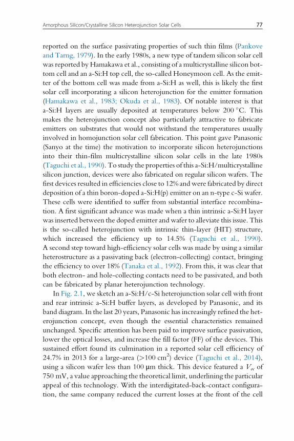
reported on the surface passivating properties of such thin films (Pankove
and Tarng, 1979). In the early 1980s, a new type of tandem silicon solar cell
was reported by Hamakawa et al., consisting of a multicrystalline silicon bot-
tom cell and an a-Si:H top cell, the so-called Honeymoon cell. As the emit-
ter of the bottom cell was made from a-Si:H as well, this is likely the first
solar cell incorporating a silicon heterojunction for the emitter formation
(Hamakawa et al., 1983; Okuda et al., 1983). Of notable interest is that
a-Si:H layers are usually deposited at temperatures below 200 �C. Thismakes the heterojunction concept also particularly attractive to fabricate
emitters on substrates that would not withstand the temperatures usually
involved in homojunction solar cell fabrication. This point gave Panasonic
(Sanyo at the time) the motivation to incorporate silicon heterojunctions
into their thin-film multicrystalline silicon solar cells in the late 1980s
(Taguchi et al., 1990). To study the properties of this a-Si:H/multicrystalline
silicon junction, devices were also fabricated on regular silicon wafers. The
first devices resulted in efficiencies close to 12% andwere fabricated by direct
deposition of a thin boron-doped a-Si:H(p) emitter on an n-type c-Si wafer.
These cells were identified to suffer from substantial interface recombina-
tion. A first significant advance was made when a thin intrinsic a-Si:H layer
was inserted between the doped emitter and wafer to alleviate this issue. This
is the so-called heterojunction with intrinsic thin-layer (HIT) structure,
which increased the efficiency up to 14.5% (Taguchi et al., 1990).
A second step toward high-efficiency solar cells was made by using a similar
heterostructure as a passivating back (electron-collecting) contact, bringing
the efficiency to over 18% (Tanaka et al., 1992). From this, it was clear that
both electron- and hole-collecting contacts need to be passivated, and both
can be fabricated by planar heterojunction technology.
In Fig. 2.1, we sketch an a-Si:H/c-Si heterojunction solar cell with front
and rear intrinsic a-Si:H buffer layers, as developed by Panasonic, and its
band diagram. In the last 20 years, Panasonic has increasingly refined the het-
erojunction concept, even though the essential characteristics remained
unchanged. Specific attention has been paid to improve surface passivation,
lower the optical losses, and increase the fill factor (FF) of the devices. This
sustained effort found its culmination in a reported solar cell efficiency of
24.7% in 2013 for a large-area (>100 cm2) device (Taguchi et al., 2014),
using a silicon wafer less than 100 μm thick. This device featured a Voc of
750 mV, a value approaching the theoretical limit, underlining the particular
appeal of this technology. With the interdigitated-back-contact configura-
tion, the same company reduced the current losses at the front of the cell
77Amorphous Silicon/Crystalline Silicon Heterojunction Solar Cells

while maintaining highVoc and FF. Panasonic recently reached an efficiency
of 25.6% for a 144 cm2 device, the highest 1-sun efficiency ever reported for
a silicon solar cell (Panasonic, 2014a).
2.1. Recombination at surfacesIn a working solar cell, generated carriers are collected at the relevant con-
tacts or they recombine.Whereas the former process constitutes the external
device current, the latter is purely a loss mechanism. Prior to either of these
two processes occurring, the generated carriers reside in the material, where
they contribute to the voltage of the device. In open-circuit conditions,
obviously no current flows, and thus the Voc is directly linked to carrier
recombination processes. Microscopically, in c-Si, bulk recombination is
usually caused by deep defects, which originate from impurities or crystal
defects. Such recombination is usually described by Shockley–Read–Hall
recombination statistics. Deep-defect recombination is also of serious con-
cern at clean silicon surfaces. The reason for this is the fact that the silicon
lattice consists of covalent Si–Si bonds that must be broken at the surface.
Depending on the precise surface orientation, each silicon surface atom will
feature either one (as on the (111) silicon surface) or two (as on the (100)
silicon surface) dangling bonds. These clean surfaces are often not stable
and may reconstruct into lower-energy configurations, which could feature,
e.g., Si–Si dimer bonds. The remaining silicon dangling bonds need to be
passivated, however. The silicon dangling bond is a so-called amphoteric
defect, which implies that it can have three different charge states. In its neu-
tral state, it contains a single electron and its energy level is approximately at
midgap, halfway between the valence band maximum and conduction band
Ag
TCO
TCO
a-Si:H (p+)a-Si:H (i)
a-Si:H (i)a-Si:H (n+)
c-Si (n)
Ag
e−h+
E
x
Figure 2.1 Schematic of a silicon heterojunction solar cell on an n-type wafer, includingits band diagram. Adapted with permission from De Wolf et al. (2012a).
78 Christophe Ballif et al.
minimum. In this state, it can give up its electron (positively charged state) or
it can host a second electron (negatively charged state). The ease with which
the dangling bond can move between these states, accepting either electrons
from the conduction band or holes from the valence band, explains its high
recombination activity and the need for surface passivation.
2.2. Physics of passivationThemicroscopic passivationmechanismof c-Si by a-Si:H ismost likely closely
linked to hydrogenation of surface states, where the hydrogen is supplied from
the passivating film. For good passivation, it is necessary that the interface
between the two materials be atomically sharp, i.e., that no epitaxial growth
has takenplace (DeWolf andKondo,2007a;Olibet et al., 2010).For such films,
low-temperature annealing can also improve the passivation properties. For
isothermal annealing, it was found that, irrespective of the precise deposition
conditions, the electronic properties always obey stretched-exponential laws
over the annealing time (DeWolf et al., 2008).Based on this, it couldbe argued
that the passivation is to a significant extent driven by microscopic
rearrangement of hydrogen close to the interface. Comparison with the bulk
properties of a-Si:H indicated that the dominant defect responsible for
recombination must be the same both in the a-Si:H bulk and at a wafer
surface, and that this defect is likely the silicon dangling bond (De Wolf
et al., 2012b). Quite generally, the passivation properties of a-Si:H films
mimic what occurs in their bulk, which includes effects such as light-induced
degradation (De Wolf et al., 2011) and doping-induced defect generation
(De Wolf and Beaucarne, 2006; De Wolf and Kondo, 2007b, 2009).
2.3. Deposition of high-quality a-Si:H filmsSince the passivating intrinsic a-Si:H layers are of such importance for the
final device, great care has to be taken during their deposition. In particular,
damage of the c-Si surface during deposition has to be limited as much as
possible. The most common way of depositing these very thin layers is
by plasma-enhanced chemical vapor deposition (PECVD), using silane
(SiH4)—often mixed with H2 for an additional source of hydrogen—as
the gas precursor, in a capacitively coupled parallel-plate reactor configura-
tion. 13.56 MHz radio frequency (RF) power is generally used for plasma
excitation (De Wolf and Kondo, 2007a; Munoz et al., 2012; Schulze
et al., 2010; Strahm et al., 2010a), but very high frequencies (VHF) of
40.68 MHz or even 70 MHz have also been applied with success for c-Si
79Amorphous Silicon/Crystalline Silicon Heterojunction Solar Cells
surface passivation (De Wolf et al., 2008; Descoeudres et al., 2013; Mueller
et al., 2010). VHF PECVD is known to have two main advantages over the
more common RF PECVD: higher deposition rates due to enhanced dis-
sociation of silane molecules, and reduced ion bombardment on the sub-
strate due to lower sheath voltages (Shah, 2010). The effect of ion
bombardment during film growth on the passivation quality is still under
debate, but it likely creates defects in the a-Si:H matrix, reducing the
a-Si:H/c-Si interface passivation (Illiberi et al., 2011). Device-grade
PECVD passivating a-Si:H films are typically deposited at temperatures of
approximately 200 �C, in the 10–100 Pa pressure range, and in the
10–100 mW/cm2 power density range. Even if thickness inhomogeneity
issues can arise in large-area (>1 m2) PECVD systems (even more critical
when using VHF rather than RF) (Howling et al., 2004; Schmitt et al.,
2002), a-Si:H depositions have already been demonstrated in industrial
systems with excellent uniformity and passivation (Strahm et al., 2010b).
The development of such industrial reactors dedicated specifically to silicon
heterojunction solar cell technology undoubtedly benefited from the
knowledge gained in recent years by the thin-film transistor and thin-film
silicon solar cell industries (Shah et al., 2013).
Other relatively similar deposition techniques have also been investi-
gated for c-Si passivation with a-Si:H, such as direct-current PECVD
(Das et al., 2008), inductively coupled PECVD (Zhou et al., 2012), hot-wire
(or catalytic) CVD (Gielis et al., 2008; Schuttauf et al., 2011; Wang et al.,
2010), electron-cyclotron-resonance CVD (Maydell et al., 2006), DC
saddle-field glow discharge (Bahardoust et al., 2010), and expanding thermal
plasma (Illiberi et al., 2010). Although some of these techniques can provide
passivation results comparable to those obtained by RF PECVD (Schuttauf
et al., 2011), the latter remains the most widespread technology at present,
mostly because of its well-proven usability at the industrial scale.
Although the passivation properties of an a-Si:H film can generally be
improved by thermal annealing (De Wolf et al., 2008; Schulze et al.,
2009), excellent passivation with layers in their as-deposited state appears nev-
ertheless to be important, mostly for layer stability over time, but also for prac-
tical reasons in the case of an industrial fabrication process. It has been reported
that device-grade, passivating intrinsic a-Si:H layers are deposited in plasma
regimes close to the amorphous-to-(micro-)crystalline transition
(Descoeudres et al., 2010); this material is similar to that required for the
intrinsic layer in thin-film silicon solar cells (Collins et al., 2003; Guozhen
et al., 2000). Such layers are generally hydrogen rich, and show a low bulk
80 Christophe Ballif et al.

defect density related to a hydrogen bonding configuration dominated by
monohydrides (Si–H) (Kroll et al., 1996, 1998). In silane-based discharges,
this transition is unequivocally determined by the actual SiH4 concentration
in the plasma, cp¼ c(1�D), with c the input SiH4 concentration and D the
SiH4 depletion fraction induced by the discharge (Strahm et al., 2007). With
the aid of plasma diagnostics such as infrared absorption spectroscopy or opti-
cal emission spectroscopy, it is indeed found that the best as-deposited a-Si:H
passivating films are obtainedwith low-cp plasmas, which correspond precisely
to amorphous regimes close to the crystalline transition (Strahm et al., 2007).
These regimes can be produced either with SiH4 plasmas highly diluted with
H2 (Gogolin et al., 2012) or with highly depleted pure SiH4 plasmas
(Descoeudres et al., 2010; Howling et al., 2010). This result underlines again
the clear role of atomic hydrogen, coming from H2 or SiH4, in the micro-
scopic passivation mechanism at the a-Si:H/c-Si interface.
As stated above, epitaxial growth has to be avoided in order to have high
passivation quality. To work in regimes close to the amorphous-to-crystalline
transition is therefore not without risk. A possible way to further approach the
transition without epitaxial growth on the c-Si surface is the use of H2 plasma
treatments, either during (Descoeudres et al., 2011) or after (Mews et al.,
2013) the a-Si:H deposition. Such treatments have several impacts on the
deposited a-Si:H material. Depending on the plasma treatment conditions,
one observes a modification of thematerial structure (either increased disorder
in the silicon network (Descoeudres et al., 2011) or improved film quality,
leading to better film stability with regard to light-induced degradation
(Sakata et al., 1993)), and an increase in the hydrogen content (Fig. 2.2),
which also widens the bandgap. Although treated a-Si:H films may be more
disordered and can contain more recombinative defects than untreated films,
the passivation quality of the crystalline substrate is generally greatly improved
due to the increased hydrogen content in the film. Hydrogen diffuses from the
bulk of the very thin a-Si:H layer toward the a-Si:H/c-Si interface, efficiently
passivating silicon dangling bonds at the interface.
Note that H2 plasma treatments before a-Si:H growth, i.e., directly on the
bare c-Si surface, lead to the creation of persistent defects at the surface and
thus to reduced passivation quality afterwards (Schuttauf et al., 2011). More
generally, the impact of any plasma species impinging on the bare surface at
plasma ignition is, to some extent, detrimental to surface passivation
(Neitzert et al., 1993). This damage created at the very early stage of the
plasma deposition process is then partly recovered by the passivating effect
of the deposited film itself. Similarly, a prolonged H2 treatment on a
81Amorphous Silicon/Crystalline Silicon Heterojunction Solar Cells

deposited a-Si:H passivating film can lead to undesirable excessive film etch-
ing. Under a critical thickness, the etched passivating layer does not ade-
quately protect the c-Si surface from the H2 plasma, and defects can also
be created underneath at the a-Si:H/c-Si interface (Geissbuhler et al.,
2013). H2 plasma treatments have also been demonstrated as a dry method
to clean the wafer surface and thus a possible alternative to the traditional
hydrofluoric acid (HF) dip before PECVD (Martın et al., 2004).
2.4. Surface passivation on n- and p-type wafersAlthough p-type c-Si is the standard material for diffused-junction solar cells
and therefore largely dominates current industrial photovoltaics production,
n-type monocrystalline silicon appears to be the best candidate for high-
efficiency solar cells and is foreseen to increase its share in c-Si photovoltaics
production in the coming years (International Technology Roadmap for
Photovoltaics, 2013). Indeed, the minority-carrier lifetime in the c-Si bulk
is usually higher in n-type than in p-type material because most metallic
0
0.1
0.2
0.3
0.4
0.5
0.6
0.7
0.8
180019002000210022002300
Wavenumber (cm−1)
Abs
orba
nce
SiH
SiH
2
SiH
2(O
2)
H2 treated layerStandard layer
Figure 2.2 Absorption spectra measured by attenuated total reflectance Fourier-transform infrared spectroscopy of 15-nm-thick H2-plasma-treated and untreateda-Si:H layers deposited on (111) c-Si wafers. Spectra are deconvoluted with twoGaussians, centered at 2000 cm�1 (monohydride bonds, stretching mode) and at2080 cm�1 (higher hydrides bonds, stretching mode). Reproduced with permission fromDescoeudres et al. (2011).
82 Christophe Ballif et al.

point defects have larger capture cross sections for electrons than for holes
(Macdonald and Geerligs, 2004). Moreover, Czochralski (CZ) n-type
wafers do not suffer from light-induced degradation, as is the case for CZ
p-type wafers when a boron–oxygen or boron–iron complex is present
(Lagowski et al., 1993; Schmidt and Cuevas, 1999). Therefore, considering
only the basic bulk properties of c-Si wafers, n-type material is better suited
to reach high conversion efficiencies.
Regarding surface passivation with a-Si:H, fundamental differences exist
between n- and p-type wafers. As with bulk defects, the capture cross sec-
tions of surface defects, i.e., dangling bonds, are larger for electrons than for
holes (Olibet et al., 2010). The same phenomenon occurs for surface defects
with thermally grown silicon dioxide (SiO2) passivation (Aberle et al.,
1992), even though the asymmetry in the respective cross sections is much
more pronounced in this case than for defects at the a-Si:H/c-Si interface. As
a result, the injection-dependent minority-carrier lifetime curves are differ-
ent for the n- and p-type cases (Fig. 2.3). A significant drop in lifetime is
observed at low injection on p-type wafers because electrons (the minority
carriers in p-type c-Si) are more easily lost at the interface than holes via
defect-assisted recombination. This behavior cannot be attributed to bulk
defects, because high-quality float-zone (FZ) wafers were used in this exper-
iment. Notably, this drop in lifetime in the p-type case has a detrimental
effect on the FF of completed solar cells (see Section 4.2). Aluminum oxide
(Al2O3) layers are better adapted to p-type wafer passivation than a-Si:H.
Higher low-injection lifetimes are obtained with such layers, due to the neg-
ative fixed charge present in this material (Hoex et al., 2008).
At high injection, on the other hand, the lifetimes are similar in both
cases, and are limited by unavoidable Auger and radiative recombination.
Thus, there is the potential to reach very high Voc values, characteristic of
the excellent surface passivation of silicon heterojunction solar cells, on both
n- and p-type wafers, as shown by the relatively similar implied Voc values
(Fig. 2.3). Such high-lifetime cells do indeed reach high injection at open
circuit under 1-sun illumination.
3. FROM PASSIVATED WAFERS TO COMPLETESOLAR CELLS
3.1. Wafer cleaning and texturingFor silicon heterojunction solar cells, the wafer of choice is usually a mono-
crystalline silicon CZ wafer that is phosphorus doped and has (100) surface
83Amorphous Silicon/Crystalline Silicon Heterojunction Solar Cells

orientation. Its thickness may vary from about 200 to 100 μm (Taguchi
et al., 2014), and it is usually pseudo-square with 600 sides if used for industrialsilicon heterojunction solar cells (Papet et al., 2013). Monocrystalline silicon
is usually preferred to multicrystalline silicon because of the higher carrier
lifetimes usually associated with the monocrystalline material. In addition,
the defined crystalline orientation of monocrystalline silicon allows for
random-pyramid texturing. Such pyramids are formed by anisotropic
etching of (100) surfaces, which reveals pyramids with (111) oriented facets
(Bean, 1978). The bases of the pyramids are usually in the range of 5–10 μm,
and the facets can feature steps but are usually quite flat. This flatness is of
considerable importance to deposit thin films of equal thickness during sub-
sequent processing. Such surfaces are almost impossible to obtain on multi-
crystalline wafers. One option for heterojunction technology on cast-silicon
10−3
10−2
1014 1015 1016
n-typep-type
Minority carrier density (cm−3)
Life
time
(s)
Implied Voc = 732 mV
Implied Voc = 730 mV
1 sun
1 sun
MPP
MPP
Auger + radiativerecombination limits
Figure 2.3 Minority-carrier effective lifetimes of silicon heterojunction solar cell precur-sors (textured wafers passivated with co-deposited i-n and i-p a-Si:H stacks) on n- andp-type 4 Ω cm FZ wafers, measured with a quasi-steady-state photoconductance sys-tem (Sinton and Cuevas, 1996). The injection levels corresponding to 1-sun illuminationare marked by solid arrows, and the corresponding implied Voc values are given. Theinjection levels corresponding to the maximum power points (MPPs) of the finisheddevices (under 1-sun illumination) are marked by the dashed arrows. Combined radia-tive and Auger recombination limits are shown by the solid lines (Richter et al., 2012;Schlangenotto et al., 1974). Reproduced with permission from Descoeudres et al. (2013).
84 Christophe Ballif et al.

wafers is to use quasi-monocrystalline silicon wafers ( Jay et al., 2012). How-
ever, suchwafers still require post-wafering processing steps such as gettering
and hydrogenation to bring the bulk carrier lifetime to acceptable levels,
casting doubt on whether this material is well suited for the fabrication of
cost-effective silicon heterojunction solar cells.
The preparation of the wafer surfaces prior to film deposition usually
consists of several steps, some of which can be combined. First, damage cau-
sed by wafer sawing is removed in an alkaline solution. Next, the typical
pyramidal texture is developed, also using an alkaline solution (Bean,
1978; Papet et al., 2006). This process is followed by wafer cleaning. Several
methods exist for this purpose, but usually the philosophy is the same: The
surfaces are wet-chemically oxidized, “encapsulating” impurities present on
the surface, and then the oxide is stripped, usually in a dilute HF bath. Dur-
ing this process, the impurities are removed, while the exposed silicon sur-
face is terminated by hydrogen atoms. This yields chemical passivation, and
can also stabilize the surface for some time following removal of the wafers
from the chemical baths. Despite this, it is usually recommended to swiftly
transfer the wafers into the deposition system.
3.2. Electron and hole collectors: Doped a-Si:H layersTo give carriers generated in the silicon wafer an incentive to be collected,
contacts specifically designed for the collection of electrons and holes must
be designed. In principle, several approaches for forming such carrier-
selective contacts exist; in silicon heterojunction solar cells, this is achieved
by depositing thin doped a-Si:H layers on the passivation layers. For elec-
tron collection, a thin phosphorus-doped a-Si:H(n) film is used, whereas
for hole collection a thin boron-doped a-Si:H(p) film is used. Though
the doping efficiency for these materials may show some asymmetry—
boron doping is well known to be difficult to achieve—the best devices
reported to date rely on this type of contact. An integral part of these con-
tacts is the transparent conductive oxide/metal stacks that are deposited on
them. The precise contact formation, including the effect of the bulk and
interface properties, has been the subject of intense study in recent years
(Bivour et al., 2013, 2014a; Favre et al., 2013; Rossler et al., 2013).
(Note that, apart from directly forming hole and electron collectors
in silicon heterojunction solar cells, highly doped a-Si:H layers can also
be used in c-Si solar cells as a phosphorus or boron dopant source for dif-
fusion into the c-Si substrate (Seiffe et al., 2013)).
85Amorphous Silicon/Crystalline Silicon Heterojunction Solar Cells
From a practical point of view, doped a-Si:H films are deposited like intrin-
sic films by PECVDwith a SiH4 andH2mixture (see Section 2.3), butwith the
addition of gases containing dopant precursors, highly diluted inH2. These are
usually diborane (B2H6) or trimethylboron (B(CH3)3) for p-type a-Si:H, and
phosphine (PH3) for n-type a-Si:H. As is well known in the thin-film silicon
solar cell community, care has to be taken regarding cross-contamination if
doped and intrinsic a-Si:H layers are successively deposited in a single PECVD
chamber. Boron or phosphorus present in the a-Si:H on the reactor walls or
substrate holder can be unintentionally incorporated into subsequent layers
(Collins, 1988; Roca i Cabarrocas et al., 1989). Such contamination leads to
poor p/i or n/i a-Si:H interface properties and is detrimental to the efficiency
of thin-film silicon solar cells. Similarly, dopant contamination in the intrinsic
a-Si:H passivation layers of silicon heterojunction solar cells leads to reduced
passivation quality and thusVoc (more severely for boron than for phosphorus
contamination). Dopants induce defects in the a-Si:H matrix, which act as
recombination centers (De Wolf and Kondo, 2009; Korte and Schmidt,
2008).To circumvent these boron andphosphorus cross-contamination issues,
several solutions have been developed (apart from using a multi-chamber
PECVD system with chambers dedicated to i-, n-, and p-layer depositions):
the deposition of a thick intrinsic coating on the reactor walls between layer
depositions (Platz et al., 1997; Xiao-Dan et al., 2009), the use of a carbon
dioxide (CO2) (Platz et al., 1997) or H2 plasma treatment (Cubero et al.,
2011; Xiao-Dan et al., 2009), or the use of an ammonia (NH3) (Ballutaud
et al., 2004) or water vapor flush (Kroll et al., 2004).
Recently, more groups have started to investigate the use of specific
electron- and hole-collecting materials that are not necessarily silicon
based. For example, molybdenum oxide (MoOx) has been used in place
of p-type a-Si:H as a hole-collecting layer. MoOx is a wide-bandgapmaterial
with a high work function. Therefore, it displays significantly higher trans-
parency in the UV than p-type a-Si:H while maintaining the role of hole
collector. With this approach, a short-circuit current density (Jsc) gain of
about 1 mA/cm2 was obtained, compared to reference cells using p-type
a-Si:H hole collectors, while maintaining a high Voc (Battaglia et al.,
2014a,b).
3.3. Transparent conductive oxide layersIn diffused-junction solar cells, the diffused emitter has a low sheet resistance
of typically 50–100 Ω/sq because of its high doping density, mobility, and
86 Christophe Ballif et al.

thickness. In silicon heterojunction solar cells, the deposited emitter is made
of low-mobility a-Si:H and it is only 5–10 nm thick. Consequently, low-
resistance lateral transport is not possible in the emitter, and—as in thin-film
solar cells that face the same obstacle—a transparent conductive oxide
(TCO) layer is required at the front side to provide a low-resistance current
path to the metal fingers. Its contribution to the lumped series resistance of
the cell, and thus to power loss through Joule heating, is proportional to its
sheet resistance, given by Rsheet¼1/enμt, where e is the electronic charge, nis the free-electron density, μ is the electron mobility, and t is the layer thick-
ness (Meier and Schroder, 1984). As in diffused-junction solar cells, sheet
resistances of 50–100 Ω/sq are required for a typical finger spacing of
approximately 2 mm if the TCO is not to contribute overwhelmingly to
the lumped series resistance. The thickness of the layer is almost always fixed
at approximately 75 nm since it then conveniently behaves as an excellent
anti-reflection coating with a reflectance minimum at 600 nm. (This is pos-
sible because most TCOs have refractive indices of approximately 2, the
geometric mean of air and silicon.) To reach the desired sheet resistance,
instead of making the TCO layer thicker, the free-electron density is instead
commonly tuned by adjusting the doping density. This approach is effective
but has a negative side effect: Parasitic absorption of infrared light by
free carriers increases with increasing free-electron density, reducing Jsc (dis-
cussed in detail later) (Holman et al., 2013a; Schroder et al., 1978).
Conversely, increasing the electron mobility reduces sheet resistance and
free-carrier absorption (Schroder et al., 1978). High-mobility TCOs are
thus the holy grail of silicon heterojunction TCO research and are an impor-
tant component of Panasonic’s success (Kinoshita et al., 2011; Taguchi et al.,
2009, 2013), but obtaining such layers is challenging.
For bifacial solar cells, the requirements for the rear TCO layer are sim-
ilar to those for the front layer, but higher TCO sheet resistance can often be
tolerated because the rear fingers are frequently closer together and the sheet
resistance that is relevant to the lumped series resistance is that of the wafer
and the rear TCO layer in parallel (assuming a front-emitter cell; for a rear-
emitter cell, this is true for the front TCO layer). For a silicon heterojunction
solar cell with full rear metallization, a TCO layer is not required for lateral
transport—in fact, it is not clear that a TCO layer is required at all. While
Bivour et al. demonstrated a 22.8% efficient rear-emitter cell without a rear
TCO layer, in which a silver rear reflector was deposited directly on a highly
doped p-layer (Bivour et al., 2012), a rear TCO layer is often included to
reduce contact resistance (Holman et al., 2013a). In addition, Holman
87Amorphous Silicon/Crystalline Silicon Heterojunction Solar Cells

et al. showed that the rear TCO layer can play an important optical role if its
thickness and carrier density are chosen correctly (Holman et al., 2013a,b,
2014). Near-bandgap p-polarized light that arrives at the rear TCO layer
above the critical angle for internal reflection creates an evanescent wave that
can be strongly absorbed in either the TCO layer itself or the subsequent
metal reflector in the form of a surface plasmon polariton. By reducing
the TCO free-electron density to n<1020 cm�3 and increasing the thick-
ness to t>100 nm, both losses are suppressed, increasing the path length
of weakly absorbed light in the wafer and thus increasing Jsc. For an
interdigitated-back-contact (IBC) silicon heterojunction solar cell, the
requirements for the rear TCO layers are the same as for cells with full rear
metallization (though electrical contact needs to be made to both n- and
p-type a-Si:H layers) and no TCO layer is required at the front.
The most commonly used TCO in silicon heterojunction solar cells is
indium tin oxide (ITO) with a tin oxide content of 5–20%. ITO is deposited
by DC or RF sputtering in an argon atmosphere, and oxygen gas is added to
tune the doping of the resulting layers through the density of oxygen vacan-
cies (Buchanan et al., 1980; Holman et al., 2013a). Figure 2.4 shows the
mobility and free-electron density, as determined from Hall-effect measure-
ments, of ITO layers sputtered at room temperature using identical condi-
tions but varying oxygen partial pressures. Two nominal film thicknesses
were investigated (left column: �120 nm; right column: �290 nm) and
the films were measured before and after curing at 200 �C, which is the finalstep in silicon heterojunction fabrication after screen printing. In all cases,
the mobility is relatively constant at a respectable but not impressive
20–40 cm2/Vs, whereas the free-electron density drops by roughly two
orders of magnitude as oxygen vacancies are filled.
To further increase mobility, researchers have explored doping indium
oxide with tungsten (IWO) (Lu et al., 2013), hydrogen (IO:H) (Barraud
et al., 2013; Koida et al., 2007, 2008, 2009, 2010, 2012), or both
(IWOH) (Kobayashi et al., 2012). Lu et al. reported a mobility of
77.8 cm2/Vs for annealed IWO (Lu et al., 2013). Koida et al. achieved
120 cm2/Vs with IO:H sputtered in an atmosphere dosed with water vapor;
they attributed the high mobility to an amorphous layer that crystallized to
form larger grains upon annealing than can be achieved in as-deposited poly-
crystalline layers (Koida et al., 2007). This result was reproduced by Barraud
et al., who fabricated a 22.1% efficient silicon heterojunction solar cell with
an IO:H front TCO layer after they identified and solved a contact resistance
problem between this layer and the screen-printed silver fingers (Barraud
88 Christophe Ballif et al.

et al., 2013). Figure 2.4 displays an IO:H layer in addition to ITO layers.
Because of IO:H’s much higher mobility, switching from the best ITO layer
in Fig. 2.4 to an IO:H layer with identical sheet resistance results in signif-
icantly less parasitic absorption (Fig. 2.5A) and a full 1.0 mA/cm2 gain in Jsc(Fig. 2.5B) (Barraud et al., 2013). Sputtered aluminum-doped zinc oxide
(ZnO) is occasionally used in silicon heterojunction solar cells in place of
indium-based TCOs (Maydell et al., 2006), but it is often too resistive (hard
to achieve high free-electron densities) and does not have particularly high
mobility.
100
120
240270300330
ITO
IO:H
B
Thi
ckne
ss (
nm) A
C
E F
D
100
120
240270300330
10
20
30
40
6080
100
Mob
ility
(cm
2 /Vs)
10
20
30
40
6080100
1018
1019
1020
1021
1018
1019
1020
1021
Thick layers
Uncured200 �C,10 min
200 �C,30 min
Car
rier
dens
ity (
cm−3
)
Plasma O2 content (%)
Thin layers
0 1 2 3 4 5 6 0 1 2 3 4 5 6
Figure 2.4 (A) and (B) Thickness, (C) and (D) mobility, and (E) and (F) free-electron den-sity of ITO and IO:H layers sputtered on glass before and after curing at 200 �C. ITO filmsof the same nominal thickness were deposited with identical conditions but varyingoxygen partial pressure. Characterization was performed with profilometry and Hall-effect measurements.
89Amorphous Silicon/Crystalline Silicon Heterojunction Solar Cells

3.4. MetallizationAs in diffused-junction solar cells, the front fingers and busbars of silicon het-
erojunction solar cells are typically screen printed; a critical difference, how-
ever, is that the paste must be curable at temperatures below 250 �C to avoid
desorbing hydrogen from the a-Si:H layers, ruining the passivation. The two
types of low-temperature paste are thermoplastic and thermoset (Zicarelli
et al., 2010). The choice of paste depends on the required solderability for
interconnection, on the targeted aspect ratio, and on the application (small
cells for research or large-area devices). Compared to high-temperature fired
paste (ρ¼3 μΩ cm), the best low-temperature paste typically reaches
8–10 μΩ cm. Silver nanopastes reach lower values but are prohibitively
expensive and are hard to print thick enough. For large-area samples
(>100 cm2), this factor of three in resistivity is a major drawback of silicon
heterojunction technology. In other words, to reach similar finger-related
losses as in diffused-junction c-Si cells, three times more paste has to be used.
An easy approach to reduce paste consumption is to increase the number of
0
5
10
15
B
IO:H,43 Ω/sq ITO,38 Ω/sq
Abs
orba
nce
(%)
A
400 600 800 1000 12000
20
40
60
80
100
IO:H, 40.0 mA/cm2
ITO, 39.0 mA/cm2
EQ
E a
nd 1
-ref
lect
ance
(%
)
Wavelength (nm)
Figure 2.5 (A) Absorbance spectra of IO:H and ITO films on glass with the same thick-ness and sheet resistance. (B) External quantum efficiency (solid) and 1-reflectance(dashed) spectra of identical silicon heterojunction solar cells with IO:H and ITO frontTCO layers. Active-area Jsc values are given. Reproduced with permission from Barraudet al. (2013).
90 Christophe Ballif et al.

busbars. An increase from three to five busbars allows, to a first approximation,
a decrease by 52/32�3 of the quantity of silver paste used for all fingers. A five-
busbar silicon heterojunction cell can, hence, have finger-related FF losses
similar to a three-busbar cell fired at high temperature. Three other
approaches to reduce silver consumption are:
1. Low-temperature copper paste: Usually, such pastes include a low-melting-
point alloy surrounding the copper particles. Some preliminary results
were demonstrated (Tokuhisa et al., 2012), but cost and reliability data
are not yet available.
2. Multi-wires: A promising approach is the use of multi-wire arrays, initially
developed by Day4 Energy and now commercialized under the name
“SmartWire.” This technology uses many wires in the place of busbars,
and the wires are “soldered” to the finger paste during the lamination
process (Fig. 2.6). The multi-wire approach is reported to reduce silver
consumption to 40 mg per side of a 600 cell (Soderstrom et al., 2013),
thanks to the relaxed requirements for finger conduction. The process
is also compatible with bifacial cells. A 320 Wmodule with a multi-wire
approach was demonstrated recently (Kobayashi et al., 2013). Addition-
ally, the multi-wire approach opens the possibility of other printing
techniques for contacts, such as inkjet or offset printing, allowing a fur-
ther reduction in silver usage (Hashimoto et al., 2013).
Figure 2.6 (A) Photograph of the multi-wire contacting scheme applied to the front fin-gers of a silicon heterojunction cell. (B) Scanning electron microscope image (preparedby using focussed ion-beammilling) of a nickel/copper finger. Shown below are energy-dispersive X-ray maps of copper, nickel, and indium, and a top-view scanning electronmicroscope image of the finger displayed above. Adapted with permission fromGeissbühler et al. (2014).
91Amorphous Silicon/Crystalline Silicon Heterojunction Solar Cells

3. Plated contacts: Several groups reported excellent results with copper-
plated contacts (Geissbuhler et al., 2014; Hernandez et al., 2013;
Munoz et al., 2012; Papet et al., 2013), including 24.2% efficient cells
by Kaneka (Hernandez et al., 2013). The ITO layer that is usually used
as the front contact and anti-reflection coating forms a good barrier
against copper diffusion and offers a natural conductor for direct plating.
In some cases, a nickel seed layer was reported to promote good adhesion
of copper fingers on the solar cells (Geissbuhler et al., 2014), as illustrated
in Fig. 2.6B. There are many approaches for creating the pattern or the
seed layer, including inkjet printing of hot-melt wax (Hermans et al.,
2013). In principle, copper metallization allows a large cost decrease
compared to three- or even five-busbar silver-printed cells. However,
it comes with the additional steps required to pattern the cell or to
remove the mask.
3.5. Record cellsIn recent years, several academic groups have started to investigate silicon
heterojunction solar cells. Meanwhile, companies have begun work on this
technology as well. In the following tables we summarize the best reported
results to date. Tables 2.1 and 2.2 show the best results on n- and p-type
wafers, respectively. Table 2.1 clearly reinforces that this technology enables
record values forVoc. Note as well that an increasing number of groups have
come very close to, or have even overcome, the 40 mA/cm2 mark for Jsc.
Additionally, several groups have clearly demonstrated that FF>80% is pos-
sible, despite prior doubts. To put these results in perspective, in Table 2.3
we show the best diffused-junction solar cells.
In Table 2.4, we show solar cells that belong to the family of hetero-
junction solar cells but have slight deviations such as a diffused front-surface
field combined with a heterojunction rear emitter; SiOx tunnel oxides
instead of intrinsic a-Si:H buffer layers; or epitaxial emitters combined with
passivating heterostructure contacts. These results underline the fact that
there are several approaches to fabricate high-efficiency silicon hetero-
junction solar cells.
Table 2.5 shows the emerging trend of combining heterojunction tech-
nology with IBC solar cells. Because no shadow losses are present and no
contacting structures are needed at the front, such a design may offer the
ultimate solution that combines high Voc and high Jsc. In 2013, Sharp pres-
ented exciting results with an IBC structure, the precise processing of which
remains undisclosed. These were followed in 2014 by the spectacular new
92 Christophe Ballif et al.
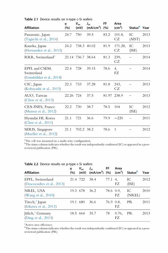
Table 2.1 Device results on n-type c-Si wafers
Affiliationη(%)
Voc(mV)
Jsc(mA/cm2)
FF(%)
Area(cm2) Statusb Year
Panasonic, Japan
(Taguchi et al., 2014)
24.7 750 39.5 83.2 101.8,
CZ
IC
(AIST)
2013
Kaneka, Japan
(Hernandez et al., 2013)
24.2 738.3 40.02 81.9 171.28,
CZ
IC
(ISE)
2013
RRR, Switzerlanda 23.14 736.7 38.64 81.3 239,
CZ
– 2014
EPFL and CSEM,
Switzerland
(Geissbuhler et al., 2014)
22.4 728 39.15 78.6 4,
FZ
– 2014
CIC, Japan
(Kobayashi et al., 2013)
22.3 733 37.28 81.8 243,
CZ
– 2013
AUO, Taiwan
(Chen et al., 2013)
22.26 724 37.5 81.97 238.9 – 2013
CEA-INES, France
(Munoz et al., 2012)
22.2 730 38.7 78.5 104 IC
(ISE)
2012
Hyundai HI, Korea
(Choi et al., 2011)
21.1 721 36.6 79.9 �220 – 2011
SERIS, Singapore
(Mueller et al., 2012)
21.1 702.2 38.2 78.6 1 – 2012
aThe cell was measured in a multi-wire configuration.bThe status column indicates whether the result was independently confirmed (IC) or appeared in a peer-reviewed publication (PR).
Table 2.2 Device results on p-type c-Si wafers
Affiliationη(%)
Voc(mV)
Jsc(mA/cm2)
FF(%)
Area(cm2) Statusb Year
EPFL, Switzerland
(Descoeudres et al., 2013)
21.4 722 38.4 77.1 4,
FZ
IC
(ISE)
2012
NREL, USA
(Wang et al., 2010)
19.3 678 36.2 78.6 0.9,
FZ
IC
(NREL)
2010
Titech,a Japan
(Irikawa et al., 2011)
19.1 680 36.6 76.9 0.8,
FZ
PR 2011
Julich,a Germany
(Ding et al., 2013)
18.5 664 35.7 78 0.76,
FZ
PR 2013
aActive-area efficiency.bThe status column indicates whether the result was independently confirmed (IC) or appeared in a peer-reviewed publication (PR).

Table 2.3 Best c-Si homojunction solar cells for p- and n-type c-Si wafers
Affiliationη(%)
Voc(mV)
Jsc(mA/cm2)
FF(%)
Area(cm2) Year
UNSW, Australia
(Zhao et al., 1996)
25 706 42.7 82.8 4, FZ, p 1998
SunPower, USA
(Cousins et al., 2010)
24.2 721 40.5 82.9 155, CZ, n 2010
Table 2.4 Notable exceptions on p- and n-type c-Si wafers
Affiliationη(%)
Voc(mV)
Jsc(mA/cm2)
FF(%)
Area(cm2) Type Statusa Year
Fraunhofer
ISE, Germany
(Heng et al.,
2013)
24.4 715 41.5 82.1 4,
FZ,
n
Diffused
front
emitter,
SiOx tunnel
oxide rear
IC
(ISE)
2014
Fraunhofer
ISE, Germany
(Bivour et al.,
2012)
22.8 705 39.9 81.5 4,
FZ,
n
Diffused
front-surface
field, rear
emitter
PR 2012
Silevo, USA
(Heng et al.,
2013)
22.1 728 38.65 78.6 155,
CZ,
n
SiOx tunnel
oxide layers
IC
(Sandia)
2013
IBM, USA
(Hekmatshoar
et al., 2012)
21.9 710 39.3 78.6 0.92,
FZ,
p
Epitaxial
emitter
PR 2012
aThe status column indicates whether the result was independently confirmed (IC) or appeared in a peer-reviewed publication (PR).
Table 2.5 Device results for IBC silicon heterojunction designs
Affiliationη(%)
Voc(mV)
Jsc(mA/cm2)
FF(%)
Area(cm2) Year
Panasonic, Japan
(Panasonic, 2014a)
25.6 740 41.8 82.7 143, n 2014
Sharp, Japan
(Koide et al., 2013)
24.7 730 41.4 81.8 3.7, n 2013
EPFL, Switzerland
(Tomasi et al., 2014)
21.5 724 39.9 74.5 9, FZ, n 2014
LG, Korea
(Lee et al., 2014)
20.5 716 37.5 76.4 221, n 2013
HZB, Germany
(Mingirulli et al., 2011)
20.2 673 39.7 75.7 1, FZ, n 2011
CEA-INES, France
(De Vecchi et al., 2012)
19.0 699 34.6 78.5 25, FZ, n 2012
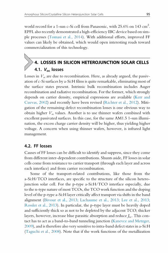
world record for a 1-sun c-Si cell from Panasonic, with 25.6% on 143 cm2.
EPFL also recently demonstrated a high-efficiency IBC device based on sim-
ple processes (Tomasi et al., 2014). With additional efforts, improved FF
values can likely be obtained, which would open interesting roads toward
commercialization of this technology.
4. LOSSES IN SILICON HETEROJUNCTION SOLAR CELLS
4.1. Voc lossesLosses in Voc are due to recombination. Here, as already argued, the passiv-
ation of c-Si surfaces by a-Si:H films is quite remarkable, eliminating most of
the surface states present. Intrinsic bulk recombination includes Auger
recombination and radiative recombination. For the former, which strongly
depends on carrier density, empirical expressions are available (Kerr and
Cuevas, 2002) and recently have been revised (Richter et al., 2012). Miti-
gation of the remaining defect recombination losses is one obvious way to
obtain higher Voc values. Another is to use thinner wafers combined with
excellent passivated surfaces. In this case, for the same AM1.5 1-sun illumi-
nation, the excess charge carrier density will be higher, thus yielding higher
voltage. A concern when using thinner wafers, however, is infrared light
management.
4.2. FF lossesCauses of FF losses can be difficult to identify and suppress, since they come
from different inter-dependent contributions. Shunts aside, FF losses in solar
cells come from resistance to carrier transport (through each layer and across
each interface) and from carrier recombination.
Some of the transport-related contributions, like those from the
a-Si:H/TCO interfaces, are specific to the structure of the silicon hetero-
junction solar cell. For the p-type a-Si:H/TCO interface especially, due
to the n-type nature of most TCOs, the TCOwork function and the doping
level of the p-type a-Si:H layer critically affect transport via shifts in the band
alignment (Bivour et al., 2013; Lachaume et al., 2013; Lee et al., 2013;
Rossler et al., 2013). In particular, the p-type layer must be heavily doped
and sufficiently thick so as not to be depleted by the adjacent TCO; thicker
layers, however, increase blue parasitic absorption and reduce Jsc. This con-
tact has to act as a band-to-band tunneling junction (Kanevce and Metzger,
2009), and is therefore also very sensitive to intra-band defect states in a-Si:H
(Taguchi et al., 2008). Note that if the work functions of the metallization
95Amorphous Silicon/Crystalline Silicon Heterojunction Solar Cells

and the doped a-Si:H layer are well matched, the TCO layer can even be
omitted without any loss in FF (Bivour et al., 2012). Another approach to
relax the constraints linked to the aforementioned FF-Jsc tradeoff is to reverse
the classical cell structure and to place the p-n junction at the rear of the cell
(rear-emitter cell). This way, the TCO and p-type a-Si:H layers can be opti-
mized mainly with respect to their electrical properties, since their optical
role in the cell is of less importance (Bivour et al., 2014b). Doing this can
reduce FF losses (Kobayashi et al., 2013). The n-type a-Si:H/TCO interface
is less critical than the p-type a-Si:H/TCO interface. An Ohmic contact for
electrons is needed, and this is relatively simple to realize in practice with
sufficient doping of the n-type a-Si:H and TCO layers.
Band offsets at the a-Si:H/c-Si interfaces also play an important role in car-
rier transport. For typical a-Si:H films, the conduction and valence band offsets
are around 0.15 and 0.45 eV, respectively, roughly independent of substrate
and film doping type (Fuhs et al., 2006; Korte and Schmidt, 2011; Schulze
et al., 2011). Nevertheless, the valence band offset increases with the a-Si:H
hydrogen content, for example, and can reach 0.6 eV (Schulze et al., 2011).
A valence band offset that is too large can have a dramatic effect on hole trans-
port, blocking carriers and reducing FF (Seif et al., 2014).
Based on the lifetime measurements shown in Fig. 2.3, FF losses from
recombinative processes can also be anticipated for heterojunction solar
cells, and are expected to be higher for p-type cells than for n-type cells.
Indeed, the minority-carrier density decreases from high to low values dur-
ing an illuminated current–voltage measurement when moving from open-
circuit to short-circuit conditions. The reduced lifetime at low injection
in the p-type case reduces performance at maximum power point (MPP)
compared to the n-type case, where the lifetime stays constant for decreasing
injection (Fig. 2.3). High Voc values are not sufficient to guarantee high FF
values: Even though n- and p-type heterojunction solar cells have similar
Voc values, cells on p-type wafers are less efficient (Descoeudres et al.,
2013). Since the minority-carrier lifetime at MPP is determined only by sur-
face recombination (provided that high-quality c-Si wafers are used), both
Voc and FF depend fundamentally on the a-Si:H/c-Si interface properties
(Descoeudres et al., 2013; Reusch et al., 2013).
4.3. Jsc lossesLosses in Jsc are caused by reflection and recombination, as well as transmis-
sion if the cell is bifacial or has interdigitated back contacts. Reflection losses
include front-surface reflection at the anti-reflection coating and metal
96 Christophe Ballif et al.
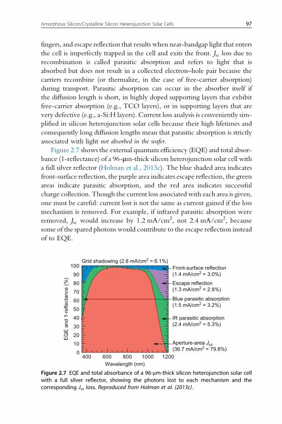
fingers, and escape reflection that results when near-bandgap light that enters
the cell is imperfectly trapped in the cell and exits the front. Jsc loss due to
recombination is called parasitic absorption and refers to light that is
absorbed but does not result in a collected electron–hole pair because the
carriers recombine (or thermalize, in the case of free-carrier absorption)
during transport. Parasitic absorption can occur in the absorber itself if
the diffusion length is short, in highly doped supporting layers that exhibit
free-carrier absorption (e.g., TCO layers), or in supporting layers that are
very defective (e.g., a-Si:H layers). Current loss analysis is conveniently sim-
plified in silicon heterojunction solar cells because their high lifetimes and
consequently long diffusion lengths mean that parasitic absorption is strictly
associated with light not absorbed in the wafer.
Figure 2.7 shows the external quantum efficiency (EQE) and total absor-
bance (1-reflectance) of a 96-μm-thick silicon heterojunction solar cell with
a full silver reflector (Holman et al., 2013c). The blue shaded area indicates
front-surface reflection, the purple area indicates escape reflection, the green
areas indicate parasitic absorption, and the red area indicates successful
charge collection. Though the current loss associated with each area is given,
one must be careful: current lost is not the same as current gained if the loss
mechanism is removed. For example, if infrared parasitic absorption were
removed, Jsc would increase by 1.2 mA/cm2, not 2.4 mA/cm2, because
some of the spared photons would contribute to the escape reflection instead
of to EQE.
400 600 800 1000 12000
10
20
30
40
50
60
70
80
90
100Grid shadowing (2.8 mA/cm2 = 6.1%)
Escape reflection(1.3 mA/cm2 = 2.8%)
IR parasitic absorption(2.4 mA/cm2 = 5.3%)
Blue parasitic absorption(1.5 mA/cm2 = 3.2%)
Front-surface reflection(1.4 mA/cm2 = 3.0%)
EQ
E a
nd 1
-ref
lect
ance
(%
)
Wavelength (nm)
Aperture-area Jsc(36.7 mA/cm2 = 79.8%)
Figure 2.7 EQE and total absorbance of a 96-μm-thick silicon heterojunction solar cellwith a full silver reflector, showing the photons lost to each mechanism and thecorresponding Jsc loss. Reproduced from Holman et al. (2013c).
97Amorphous Silicon/Crystalline Silicon Heterojunction Solar Cells

Shadowing from the front metal grid creates the largest Jsc loss. Reducing
it by narrowing the finger and busbars improves cell performance only if
they are simultaneously made taller or more conductive so that their con-
tribution to the lumped series resistance does not increase. Stencil printing
is one approach to achieve higher-aspect-ratio metal lines (Zicarelli et al.,
2010), and copper plating is one approach to achieve more conductive lines
(Hernandez et al., 2013); both are described in detail in other sections.
Parasitic absorption of blue light is responsible for the next largest loss,
and is due to absorption in the front a-Si:H layers (Fujiwara and Kondo,
2007; Holman et al., 2012; Jensen et al., 2002; Page et al., 2011; Psych
et al., 2010; Tanaka et al., 1992). All light absorbed in the defective
p-type layer is lost via fast recombination of carriers, as is 70% of light
absorbed in the intrinsic layer; blue absorption in the front TCO layer is
small because of its wide bandgap (Holman et al., 2012). The simplest fix
is to make these layers thinner, but this comes at a price. If the intrinsic layer
thickness drops below approximately 4 nm, it is no longer able to effectively
passivate the surface because the electron wavefunction in the wafer pene-
trates through it and Voc drops (Fujiwara and Kondo, 2007; Holman et al.,
2012; Tanaka et al., 1992). If the p-type layer is made thin, FF falls, which
Bivour et al. have attributed to its becoming depleted by the heavily doped
n-type front TCO, reducing band bending in the wafer (Bivour et al., 2013).
An alternative approach is to make the front a-Si:H layers more transparent
by either widening the bandgap by alloying with oxygen or carbon (Einsele
et al., 2012; Mueller et al., 2010; Seif et al., 2014), or making the bandgap
indirect by growing microcrystalline silicon (μc-Si:H) (Ding et al., 2012;
Olibet et al., 2010). The former approach is challenging because FF often
falls as carrier transport is inhibited by larger band offsets, and the latter
approach is challenging because μc-Si:H often has an amorphous incubation
layer when grown on a-Si:H. Both remain active areas of research, spurred
on by recent success with wide-bandgap layers by Fraunhofer ISE and Silevo
(Feldman et al., 2014; Heng et al., 2013). Yet another approach is to change
the device design so that all of the a-Si:H layers are at the rear (interdigitated
back contacts) or at least the p-layer is at the rear (rear emitter) so that the
n-layer at the front can be very thin without being depleted.
The final large Jsc loss is due to infrared parasitic absorption. This light
bounces around many times in the solar cell, and is absorbed parasitically
by free carriers in both the front and rear TCO layers, as well as in the rear
metal reflector (Holman et al., 2013a,b, 2014). As the front TCO layer must
meet a stringent sheet-resistance requirement while the rear TCO layer can
98 Christophe Ballif et al.
be made resistive and transparent, the front TCO often dominates the losses
and the only route to improvement is higher mobilities (Holman et al.,
2013a). The rear metal reflector is also lossy—even for an excellent reflector
like silver—for p-polarized light arriving at the back surface (with respect to
the appropriate pyramid facet) above the critical angle for internal reflection.
These photons are not totally internally reflected; instead they undergo atten-
uated internal reflection (as in a Fourier transform infrared spectroscopy
measurement performed in the attenuated total reflection mode) because
the evanescent wave interacts with lossy rather than perfectly transparent
media (the TCO and metal layers) (Harrick and Dupre, 1966; Holman
et al., 2013a; Otto, 1968). In particular, if the evanescent wave reaches
the metal reflector it will excite surface plasmon polaritons that absorb
the incident photon energy. This is remedied by displacing the reflector
from the back of the solar cells by at least the evanescent wave’s penetration
depth with a transparent rear TCO layer or a dielectric with local openings
(Holman et al., 2013c).
Imperfect light trapping—taken here to mean the path length enhance-
ment of light in the wafer in the absence of absorption—is not as large a loss
as is commonly thought. The random-pyramid texture that is common in all
industrial monocrystalline silicon solar cells is so effective that only approx-
imately 0.5 mA/cm2 (depending on the wafer thickness) would be gained if
the wafers had perfectly Lambertian surfaces (Yablonovitch, 1982). Never-
theless, Ingenito et al. recently demonstrated a path to come even closer to
the Lambertian limit using periodic arrays of pyramids of different sizes and
shapes at the front and rear surfaces (Ingenito et al., 2014). Front surface
reflectance is also not a particularly large Jsc loss after encapsulation because
the glass and polymer of the module introduce another, intermediate refrac-
tive index. Consequently, double-layer anti-reflection coatings are
seldom used.
5. INDUSTRIALIZATION AND COMMERCIALIZATION
5.1. General statusThe first silicon heterojunction products were sold by Sanyo in 1997. Their
current annual production capacities reached approximately 900 MW at the
end of 2013 (now under Panasonic). Research activities in the field
started at various institutes in 2004–2005, first with the demonstration of
high Voc values (i.e., over 700 mV) (Olibet et al., 2007), and later with dem-
onstrations of devices exceeding 22% efficiency (Bivour et al., 2014b;
99Amorphous Silicon/Crystalline Silicon Heterojunction Solar Cells
Descoeudres et al., 2013; Munoz et al., 2012; Schulze et al., 2011). At the
same time, the expiration of key Sanyo patents triggered renewed interest
from several industrial actors. Since 2013, companies such as Silevo have
marketed modules with cells based on a silicon heterojunction-like structure
(with the addition of SiOx tunneling layers) and with typical cell efficiencies
of over 21%. Sunpreme offers bifacial modules based on silicon hetero-
junction solar cells on 500 wafers. Choshu Industry Co., Ltd. (CIC) has also
set up a 30 MW production line and has demonstrated 22.3% efficient, 600,full-area, rear-emitter cells. CIC also demonstrated 320 W 60-cell R&D
modules (Kobayashi et al., 2013). CEA-INES is piloting a line with a nom-
inal capacity of 18 MW (Ribeyron, 2014). The equipment maker Roth and
Rau (now underMeyer Burger) has developed PECVD and sputtering tools
specifically for silicon heterojunction cell mass manufacturing, and demon-
strated 22.3% efficient solar cells on 600 CZwafers. They have indicated a takt
time of approximately 90 s for 56 wafers per carrier in production. Several
industrial and research labs have exceeded the 21% efficiency barrier with
devices greater than 100 cm2 in size, and the availability of production
equipment is making the technology available for mass industrialization.
5.2. Material requirementsThe strength of silicon heterojunction solar cells is their high Voc values of
725–750 mV for wafer thicknesses of 100–160 μm. To obtain such high
voltages, minority-carrier bulk lifetimes in the millisecond range are
required. This is typically achieved using n-type CZ material. Some groups
have also reported good results with properly processed n-type quasi-mono
wafers ( Jay et al., 2012, 2014). As discussed previously, n-type c-Si material
is chosen for two reasons: It is generally less sensitive to metal impurities than
p-type c-Si, and it is not sensitive to the boron–oxygen complex (Glunz
et al., 2001; Korte and Schmidt, 2011; Schmidt and Cuevas, 1999). For
p-type c-Si, good devices on FZ p-type wafers with Voc over 720 mV have
also been reported (Descoeudres et al., 2013) but the devices made on CZ
p-type wafers suffered from low lifetimes and possible defects in the space
charge region. Several wafer manufacturers have demonstrated the capabil-
ity to grow full n-type CZ ingots with bulk lifetimes in excess of several mil-
liseconds, even after multiple charge pulling. The company MEMC has
shown that continuous CZ pulling (CCZ) (Li, 2013) allows for the growth
of 9-m-long ingots with lifetimes decreasing from 10 to 2 ms. Figure 2.8
shows the simulated impact of bulk lifetime on the efficiency of typical
100 Christophe Ballif et al.

silicon heterojunction solar cells with thicknesses of 120 μm. The model,
implemented in the one-dimensional device simulator PC1D, is described
in Ballif et al. (2012), and assumes low-mobility doped layers to mimic the
role of a-Si:H heterointerfaces. Above a bulk lifetime of 4 ms, there is only a
marginal difference in efficiency between the three doping levels. The cells
still have above 21% efficiency at 800 μs lifetime (whatever the doping) and
the efficiency saturates at 22.3% for a lifetime above 4 ms. If processed cor-
rectly, the full 9-m-long CCZ ingot pulled by MEMC would lead to an
average cell efficiency of around 22%. All of the values reported here were
obtained with a nominal Voc of 732 mV (for a 4 ms bulk lifetime), Jsc of
37.8 mA/cm2, and FF of 79.9%. Notably, as silicon heterojunction solar
cells operate close to high-injection conditions at MPP and both surfaces
have full-area contacts, the base doping is less critical to the series resistance
than in passivated emitter and rear contact (PERC) cells. Consequently, a
larger doping variation—like that obtained in typical n-type ingot
growth—can be tolerated. Figure 2.9 shows simulated cell efficiency as a
function of doping for an improved device with quasi-perfect passivating
contacts. The results are displayed for various bulk lifetimes and wafer thick-
ness. For a cell with a thickness of 100 μm, a bulk lifetime of 4 ms, and a
wafer resistivity of 3 Ω cm, we anticipate a nominal efficiency of 25%, a
Voc of 755 mV, a Jsc of 39.9 mA/cm2, and a FF of 83.3%, which are in
the range of the best reported results from Panasonic (Taguchi et al.,
2014). The plot shows that, as expected, for quasi-perfect contacts and high
100 1000 10,00017
18
19
20
21
22
23
1 Ωcm 4 Ωcm
10 Ωcm
Cel
l effi
cien
cy (
%)
Bulk lifetime (μs)
Wafer resistivity
Figure 2.8 Efficiency of standard silicon heterojunction cells as a function of bulklifetime. The simulations were performed with PC1D using a model presented inBallif et al. (2012).
101Amorphous Silicon/Crystalline Silicon Heterojunction Solar Cells

lifetime, the doping and thickness no longer play any role. For reduced bulk
lifetimes, thinner wafers and higher base doping mitigate the losses, leading
to efficiencies between 23.5% and 25.5%. Finally, depending on the initial
quality of the silicon wafer, material improvements can be obtained by
gettering or hydrogenation. CIC also reported the use of a thermal-donor
annealing step.
5.3. Temperature coefficient and energy yieldThe high Voc grants silicon heterojunctions an improved temperature coef-
ficient (Green, 1998), and typical values of �0.2–0.3%/�C at MPP have
been reported (Batzner et al., 2011; Heng et al., 2013; Mishima et al.,
2011; Taguchi et al., 2014). Indeed, coefficients as low as �0.1%/�C(Seif et al., 2014) were reported in the range of 25–55 �C. The discrepanciesbetween the values for cells with equivalent Voc stem from the properties of
the a-Si:H layers and from the temperature dependence of the FF: Transport
through the heterocontacts can be improved by the temperature in some
cases, leading to a stable or even increased FF with the temperature and,
hence, to a more favorable temperature coefficient. Note that in such cases,
however, the efficiency in standard test conditions might also be lower than
for cells without activated transport. In general, the lower temperature coef-
ficient of silicon heterojunction cells should ensure—depending on
the climate—a typical energy gain of 3–5% relative to standard c-Si
1012 1013 1014 1015 1016 101723.0
23.5
24.0
24.5
25.0
25.5
26.0
10 ms, 150 μm10 ms, 100 μm
1 ms, 60 μm1 ms, 100 μm1 ms, 150 μm
Cel
l effi
cien
cy (
%)
Wafer doping density (cm−3)
Bulk lifetime, wafer thickness
Figure 2.9 Efficiency of state-of-the-art silicon heterojunction cells as a function ofbackground doping and for various bulk lifetime and wafer thickness combinations.The simulations were also performed with PC1D.
102 Christophe Ballif et al.

diffused-junction cells with�0.45%/�C. The high efficiency (reduced ther-malization and increased reflection of sub-bandgap light) also translates into a
lower operating temperature of the modules by 2–3 �C, giving an additionalenergy gain of 0.4–0.7% (Kurnik et al., 2011). As silicon heterojunction cells
have no fired contacts and no second-diode current (so-called J02), they
show near-perfect low-illumination behavior, giving a gain of around
1–2% compared to cells with fired contacts. This can increase energy yield
by 4–8%, depending on the location and climate. For building-integrated
photovoltaics (BIPV), where the operating temperature may be 15–20 �Chigher (Kurnik et al., 2011), an additional energy gain of 3–4% can be
expected.
5.4. MetallizationSeveral approaches to metalizing silicon heterojunction solar cells have been
presented previously. For production, screen printing is simple and reliable
and is therefore commonly used. However, the minimum finger width pos-
sible with screen printing is approximately 70 μm, resulting in shadowing
losses of 5–8%, and a lot of paste must be used because of its comparatively
high resistivity. Replacing busbars with multi-wires reduces the silver
required for the finger, but the cost of the low-temperature soldering alloy
might partly offset the reduced silver usage. In the long term, plating may be
the best option for high efficiencies at low cost. However, the additional
process complexity and moderate efficiency improvement, compared to
screen printing, might delay its introduction until silver becomes signifi-
cantly more expensive.
The metallization scheme selected, together with the cells’ contacting
layers (e.g., ITO, silver or nickel vanadium), impacts the choice of both
the interconnection method (soldering or gluing) and the module packaging
materials. In particular, soldering on low-temperature paste is a more
delicate process than on high-temperature paste, and alternative approaches,
e.g., with conductive adhesives, are also used by some companies. Notably,
the packaging of silicon heterojunction modules can benefit from many of
the approaches developed for thin-film technology, in which TCOs and
low-temperature pastes are also present.
5.5. Tools and production technologiesIn its most simple form, silicon heterojunction technology requires a mix of
traditional and new pieces of equipment. We describe here some of the key
103Amorphous Silicon/Crystalline Silicon Heterojunction Solar Cells

steps for solar cell manufacturing and, when relevant, some features of the
tools. We note that several device configurations are possible. By nature, sil-
icon heterojunction cells can be made with the emitter at the front or at the
rear of the cell, and excellent results have been reported in both configura-
tions (Descoeudres et al., 2013). This translates into an intrinsic bifaciality
that can be employed, e.g., by printing silver lines directly onto the front
and rear of the solar cells.
5.5.1 Wet chemistryAs described in Section 3.1, most reported approaches rely on a standard
saw-damage etch following by random-pyramid texturing (or these pro-
cesses are performed simultaneously) followed by surface cleaning. Immedi-
ately prior to a-Si:H deposition, the wafer is dipped in a diluted HF solution
to strip the oxide. The texturing and cleaning can strongly impact the solar
cell performance, requiring good control of the chemical quality. Though
some cleaning recipes have been reported (Edwards et al., 2008; Page
et al., 2006), most texturing and cleaning processes are proprietary.
5.5.2 a-Si:H layer depositionSeveral deposition techniques have been reported to provide high-quality
a-Si:H passivation layers including microwave PECVD ( Jeon and
Kamisako, 2009), inductively coupled plasmas (Psych et al., 2010; Xiao
et al., 2012), and hot-wire CVD (Branz et al., 2008; Schuttauf et al.,
2011; Schuttauf et al., 2011). For devices with over 21% efficiency, the main
reported techniques are based on parallel-plate capacitively coupled
PECVD. Good results have been reported both at 13.56 and 40.68 MHz
(Descoeudres et al., 2011). An advantage of parallel-plate PECVD is the
direct transfer of knowledge gained from thin-film silicon films for, e.g.,
doped layer deposition.
Achieving homogeneity (5–10% thickness variation) in a large-area
plasma reactor (>1 m2) is a problem that has been solved by the flat-panel
display and thin-film silicon PV industries. Careful PECVD reactor design is
required to ensure uniform gas distribution and a uniform plasma even close
to the electrode edges (Howling et al., 2005). If frequencies of 40 MHz or
higher are used, inhomogeneities should be compensated by “lenses” for
large-area reactors (Sansonnens and Schmitt, 2003; Schmidt et al., 2004).
The typical deposition rate of a-Si:H layers is in the range of
0.2–0.5 nm/s. It can be inferred that process times below 1 min are achiev-
able for each of the four a-Si:H layers (i, n, i, p) deposited in a standard silicon
heterojunction solar cell. As a first approximation, assuming 60 600 wafers per
104 Christophe Ballif et al.

batch, a well-designed production system should have four PECVD cham-
bers. It should process such batches with a takt time of 90–120 s, including
handling, giving a nominal annual capacity of 60–100 MW, depending on
the uptime.
If the samples are transported on carriers, there is the possibility of con-
tamination of the chamber with a reused carrier. Therefore carrier and con-
tamination management can play an important role in achieving good
results. Figure 2.10 is an example of a PECVD tool with a central unit used
to exchange the wafers from carriers.
5.5.3 Front and rear TCO, and rear metallizationPlasma-assisted evaporation (ion-beam plating) (Kobayashi et al., 2012,
2013) and sputtering (Batzner et al., 2011; Descoeudres et al., 2013;
Harrison et al., 2011; Hernandez et al., 2013; Lachenal et al., 2010) have
been reported as effective methods for depositing the front and rear TCO
layers. Sputtering is a well-established method, and the use of a rotary mag-
netron allows for effective target usage (>70%).With open carriers, the front
and rear sides of wafers can be coated in the same run. Most reports have
focused on the use of ITO as a TCO, even though ZnO has also been used
Figure 2.10 Example of a PECVD system with a lateral processing chamber. Each cham-ber has a dedicated carrier. The system has a nominal throughput of 2400 600 wafersper hour. Image courtesy of Meyer Burger/Roth and Rau.
105Amorphous Silicon/Crystalline Silicon Heterojunction Solar Cells

in silicon heterojunctions (Maydell et al., 2006; Munoz et al., 2011) as both
the front and rear TCO. ZnO deposited by low-pressure CVD was also
reported (Choong et al., 2010). High-efficiency devices require careful opti-
mization of the transparency of the TCO (e.g., with oxygen control) and
proper control of the surface dopant density to ensure good contact with
subsequent metallization (Barraud et al., 2013). The TCO at the rear also
acts as a natural rear reflector. The optical properties of silicon hetero-
junctions have been discussed in detail in previous sections and by
Holman et al. (2012, 2013a,c). In particular, if the rear TCO is strongly
doped, its thickness should be minimized to avoid free-carrier absorption
in it; if it is lightly doped, it should be >100 nm thick to suppress plasmon
excitation in the rear metal reflector. However, in this case, the gain in Jscand hence efficiency may be offset by the additional material and equipment
costs, and implementation of ideal reflectors in industrial cells will depend on
the achievable deposition rates and material costs.
In bifacial and IBC cells with screen-printed silver fingers on the rear
TCO, a white or transparent backsheet can be used. A white rear reflector
exhibits no plasmonic loss (unlike silver) and also promotes high Jsc.
However, if the silver fingers are spaced too far apart, some FF losses
will occur.
5.5.4 Final processingAfter printing, the cells are typically cured at a temperature below 250 �Cfor 10–20 min. This step reduces the finger and busbar line resistance,
can promote a mobility (and thus transparency) increase in the TCO
(Figure 2.4), and anneals the defects induced in the a-Si:H layers by the
sputtering process (Demaurex et al., 2012). After curing, measurement
of cell current–voltage characteristics requires a different setup than that
used for diffused-junction cells. Because of the high Voc and associated dif-
fusion capacitance (Beljean et al., 2011; Feretti et al., 2013), an illumination
length in excess of several hundred milliseconds is preferred, which is too
long for the flashers usually used in production lines. One approach to
properly measure a cell is to use a flasher to measure Jsc only, because tran-
sient effects are limited in short-circuit conditions. To subsequently sweep
the current–voltage curve, continuous (and often monochromatic) LED
lighting is used with an intensity set to provide the same Jsc. A sweep time
of 150–700 ms can be required, depending on the device and on the spe-
cific measurement procedures.
106 Christophe Ballif et al.

5.6. Production costsThe production costs for silicon heterojunction solar cells can be assessed
relatively simply. High-quality n-type CZ material can require some adap-
tation of the pulling process (slower speed) and good-quality feedstock. The
combination of thin wafers (sawn to 140 μm in the foreseeable future with
the potential for 120 and 100 μm farther out) and diamond sawing can lead
to competitive n-type wafer pricing comparable to standard p-type CZ
material. Compared to a diffused-junction production line, the PECVD
and sputtering tools are different, replacing the diffusion furnace, dielectric
(e.g., silicon nitride) coating tool, rear-side etching and edge isolation sta-
tions, and rear-side printer. In a reasonable time frame, the cost for 1 m2
PECVD reactors and TCO or metal coating tools should come down to
€1 to 2 million. Such tools have been heavily developed for the glass-coating
industry, e.g., for flat-panel displays. Thus, in terms of process equipment
capital expenditures, silicon heterojunction production lines should be able
to approach diffused-junction lines that include selective emitters or rear-
side passivation with local openings.
Themajor production costs for siliconheterojunction technology include
the depreciation of the equipment, the targets (especially ITOand silver), and
thematerial costs of themodules. Table 2.6 gives an estimate of the cost of the
transformation of wafers to modules. This model assumes a monocrystalline
600 wafer (240 cm2), a multi-wire interconnection scheme, and cell produc-
tion costs that include 40 mg of silver paste and 80 nm of ITO on both sides.
Table 2.6 Estimated direct manufacturing costs for a typical 500–1000 MW cell andmodule manufacturing lineType of cost Cost in €cts/Wp
Wafer 14–18
Depreciation of equipment and buildings 4–7
Direct personnel costs 1–2
Materials and operation, cells 4–6
Materials and operation, modules 12–16
Electricity 0.2–0.4
Total manufacturing costs 35–49
A high yield of 95% is assumed for the cell and module lines and the average cell efficiency is assumedto be 22%. The exact numbers depend on location, the specific choice of tools, and the metallizationapproach. The depreciation period is assumed to be six years for the production lines and 20 years forthe buildings and facilities.
107Amorphous Silicon/Crystalline Silicon Heterojunction Solar Cells
Considering the target module efficiency and reduced balance-of-system
costs, together with the expected high energy yield, an ultra-low levelized
cost of electricity (LCOE) is anticipated, typically below 4€cts/kWh in a
sunny country. With potential efficiency improvements, replacement of
ITOwith indium-free materials, and a further decrease in wafer and module
material costs, a further decrease of 10% can be expected in the cost of elec-
tricity production.
6. FUTURE DIRECTIONS AND OUTLOOK
Table 2.7 summarizes some of the strengths and weaknesses of silicon
heterojunction technology. In principle, the limited number of cell
processing steps and the near-infinite possibilities offered by the plasma
processes used to make the passivating layers and electron and hole collec-
tors offer the prospect of a simple and low-cost production technology that
yields high-efficiency cells. 320 W 60-cell modules have already been
demonstrated (Kobayashi et al., 2013) and commercial modules with
19.4% efficiency are commercially available (Panasonic, 2014b). Several
companies are entering production with tens-of-MW lines and many more
are assessing the technology using pilot or advanced R&D tools. Silicon
heterojunction technology has the possibility to rival the more standard
PERC (Blakers et al., 1989) or PERL (Green, 1991) approach in terms
of manufacturing costs, but with an upside potential for high efficiency.
This, coupled with their high energy yield, should allow silicon hetero-
junction modules to achieve reduced LCOE in solar farms. For space-
constrained installations, their higher efficiency translates into higher selling
prices, which should enable companies to generate a higher return on
investment. Silicon heterojunction modules, with their low-temperature
coefficient, could also earn a leading role in the built environment if the
BIPV market realizes its long-awaited growth potential. Most of the per-
ceived challenges, such as unstable processes for contact formation or the
need for high-quality surface cleaning, can be turned into a competitive
advantage in the form of proprietary processes that are not easy to copy.
However, a real challenge for silicon heterojunction cells is to enter into
the market with high enough volume to surpass the existing players. Most
companies prefer to continue with well-established technologies and favor
upgrades of existing standard, diffused-junction lines, which can be depre-
ciated faster and do not have the risk of a technology step. With the clear
potential for 60-cell modules with a power of 320 W (or more), silicon
heterojunction cells, once established, may force companies to adopt
108 Christophe Ballif et al.

similar or other advanced technologies. At the cost of some modified or
added steps, silicon heterojunction cells could also evolve. An attractive
candidate is the IBC cell design, which nearly eliminates parasitic losses
at the front while maintaining ultra-high Voc. Indeed a 25.6% cell effi-
ciency was reported recently using such an approach, taking full advantage
of the concept of passivating contacts (Panasonic, 2014a). More generally,
a-Si:H-based contacts are paving the way for low-temperature and efficient
passivating contacts on all cells—including diffused-junction cells.
Table 2.7 Some of the key features of silicon heterojunction technologiesStrengths Challenges Opportunities
High efficiency in
production, potentially up
to >24%
Requires high-quality
ingots (with
correspondingly higher
cost/kg)
Less sensitive to base
doping level, ideal for thin
wafers
Intrinsic high energy yield,
thanks to temperature
coefficient and low-
illumination behavior
Low levelized cost of
energy, well suited to BIPV
sector
Few process steps Requires good process
control
Proprietary production
processes/differentiation
Low-temperature
processes, no stress
Requires high-quality
surface preparation
Proprietary production
processes
Use of established low cost/
m2 coating technology
Requires quality
production tools
(homogeneity,
repeatability, control)
Potential for low capital
expenditures for
production equipment
Compatible with thin
wafers and diamond sawing
Maintaining high
production yield with
thin wafers
Cell design is intrinsically
bifacial, different products
with minor changes
Basic versions require
ITO, which may
increase costs
Use of ITO as a barrier for
plating, substitute ITO
with other TCOs
By definition, cells are not
subject to potential-
induced degradation
Requires dedicated
encapsulation process
Optimized module lifetime
and reliability, benefitting
from knowledge of thin-
film cells
Potentially low production
costs
Mass manufacturing
experience still limited
to a few manufacturers
Higher market price of
high-efficiency modules
109Amorphous Silicon/Crystalline Silicon Heterojunction Solar Cells

ACKNOWLEDGMENTSThe authors thank B. Demaurex, J. Geissbuhler, J. Seif, and A. Tomasi for support in
manuscript preparation. We also acknowledge support from the EU-FP7 program and the
Swiss Federal Office for Energy.
REFERENCESAberle, A.G., Glunz, S., Warta, W., 1992. Impact of illumination level and oxide parameters
on Shockley–Read–Hall recombination at the Si–SiO2 interface. J. Appl. Phys.71, 4422–4431.
Agostinelli, G., Delabie, A., Vitanov, P., Alexieva, Z., Dekkers, H.F.W., De Wolf, S.,Beaucarne, G., 2006. Very low surface recombination velocities on p-type silicon waferspassivated with a dielectric with fixed negative charge. Sol. Energy Mater. Sol. C90, 3438–3443.
Bahardoust, B., Chutinan, A., Leong, K., Gougam, A.B., Yeghikyan, D., Kosteski, T.,Kherani, N.P., Zukotynski, S., 2010. Passivation study of the amorphous–crystalline sil-icon interface formed using DC saddle-field glow discharge. Phys. Status Solidi A207, 539–543.
Ballif, C., Barraud, L., Descoeudres, A., Holman, Z.C., Morel, S., De Wolf, S., 2012. A-Si:H/c-Si heterojunctions: a future mainstream technology for high-efficiency crystallinesilicon solar cells? In: 2012 38th IEEE Photovoltaic Specialists Conference (PVSC),pp. 001705–001709.
Ballutaud, J., Bucher, C., Hollenstein, C., Howling, A.A., Kroll, U., Benagli, S., Shah, A.,Buechel, A., 2004. Reduction of the boron cross-contamination for plasma deposition ofp-i-n devices in a single-chamber large area radio-frequency reactor. Thin Solid Films468, 222–225.
Barraud, L., Holman, Z.C., Badel, N., Reiss, P., Descoeudres, A., Battaglia, C., DeWolf, S.,Ballif, C., 2013. Hydrogen-doped indium oxide/indium tin oxide bilayers for high-efficiency silicon heterojunction solar cells. Sol. Energy Mater. Sol. C 115, 151–156.
Battaglia, C., Yin, X., Zheng, M., Sharp, I.D., Chen, T., McDonnell, S., Azcatl, A.,Carraro, C., Ma, B., Maboudian, R., Wallace, R.M., Javey, A., 2014a. Hole selectiveMoOx contact for silicon solar cells. Nano Lett. 14, 967–971.
Battaglia, C., de Nicolas, S.M., DeWolf, S., Yin, X., Zheng, M., Ballif, C., Javey, A., 2014b.Silicon heterojunction solar cell with passivated hole selective MoOx contact. Appl.Phys. Lett. 104, 113902.
Batzner, D., Andrault, Y., Andreetta, L., Buechel, A., Frammelsberger, W., Guerin, C.,Holm, N., Lachenal, D., Meixenberger, J., Papet, P., Rau, B., Strahm, B.,Wahli, G., Wuensch, F., 2011. Characterization of over 21% efficient silicon hetero-junction solar cells developed at Roth & Rau Switzerland. In: EU PVSEC, Hamberg,Germany.
Bean, K.E., 1978. Anisotropic etching of silicon. IEEE Trans. Electron Devices25, 1185–1193.
Beljean, P.-R., Lo, A., Despeisse, M., Riesen, Y., Pelet, Y., Fakhfouri, V., Wyrsch, N.,Ballif, C., 2011. I/V measurement of high capacitance cells with various methods.In: 26th European Photovoltaic Solar Energy Conference, Frankfurt, Germany,pp. 3275–3278.
Benick, J., Zimmermann, K., Spiegelman, J., Hermle, M., Glunz, S.W., 2011. Rear side pas-sivation of PERC-type solar cells by wet oxides grown from purified steam. Prog. Pho-tovoltaics Res. Appl. 19, 361–365.
Bivour, M., Reichel, C., Hermle, M., Glunz, S.W., 2012. Improving the a-Si:H(p) rearemitter contact of n-type silicon solar cells. Sol. Energy Mater. Sol. C 106, 11–16.
110 Christophe Ballif et al.

Bivour, M., Schr€oer, S., Hermle, M., 2013. Numerical analysis of electrical TCO/a-Si:H(p) contact properties for silicon heterojunction solar cells. Energy Procedia38, 658–669.
Bivour, M., Reusch, M., Schroer, S., Feldmann, F., Temmler, J., Steinkemper, H.,Hermle, M., 2014a. Doped layer optimization for silicon heterojunctions byinjection-level-dependent open-circuit voltage measurements. IEEE J. Photovoltaics4, 566–574.
Bivour, M., Schr€oer, S., Hermle, M., Glunz, S.W., 2014b. Silicon heterojunction rear emit-ter solar cells: less restrictions on the optoelectrical properties of front side TCOs. Sol.Energy Mater. Sol. C 122, 120–129.
Blakers, A.W., Wang, A., Milne, A.M., Zhao, J.H., Green, M.A., 1989. 22.8% efficient sil-icon solar cell. Appl. Phys. Lett. 55, 1363–1365.
Branz, H.M., Teplin, C.W., Young, D.L., Page, M.R., Iwaniczko, E., Roybal, L.,Bauer, R., Mahan, A.H., Xu, Y., Stradins, P., Wang, T., Wang, Q., 2008. Recentadvances in hot-wire CVD R&D at NREL: from 18% silicon heterojunction cells tosilicon epitaxy at glass-compatible temperatures. Thin Solid Films 516, 743–746.
Buchanan, M., Webb, J.B., Williams, D.F., 1980. Preparation of conducting and transparentthin films of tin-doped indium oxide by magnetron sputtering. Appl. Phys. Lett.37, 213–215.
Chen, M.-Y., Chang, Y.-L., Yang, P.-C., Huang, M.-Y., Chien, Y.-J., Liu, J.S.Q.,Chang, J., 2013. Effects of intrinsic a-Si:H layer on the performance of silicon hetero-junction solar cells. In: 28th European Photovoltaic Solar Energy Conference, Paris,France.
Choi, J.H., Kim, S.K., Lee, J.C., Park, H., Lee, W.J., Cho, E.C., 2011. Advanced modulefabrication of silicon heterojunction solar cells using anisotropic conductive filmmethod.In: 26th European Photovoltaic Solar Energy Conference, Hamburg, Germany, p. 3302.
Choong, G., Bole, P., Barraud, L., Zicarelli, F., Descoeudres, A., De Wolf, S., Ballif, C.,2010. Transparent conductive oxides for silicon heterojunction solar cells. In: EUPVSEC, Valencia, Spain, pp. 2505–2510.
Collins, R.W., 1988. In situ study of p-type amorphous silicon growth from B2H6:SiH4mix-tures: surface reactivity and interface effects. Appl. Phys. Lett. 53, 1086–1088.
Collins, R.W., Ferlauto, A.S., Ferreira, G.M., Chen, C., Koh, J., Koval, R.J., Lee, Y.,Pearce, J.M., Wronski, C.R., 2003. Evolution of microstructure and phase in amor-phous, protocrystalline, and micro crystalline silicon studied by real time spectroscopicellipsometry. Sol. Energy Mater. Sol. Cells 78, 143–180.
Cousins, P.J., Smith, D.D., Luan, H.C., Manning, J., Dennis, T.D., Waldhauer, A.,Wilson, K.E., Harley, G., Mulligan, W.P., 2010. Generation 3: Improved performanceat lower cost. In: 35th IEEE Photovoltaic Specialists Conference, Honolulu, HI, p. 275.
Cubero, O., Haug, F.J., Ziegler, Y., Sansonnens, L., Couty, P., Fischer, D., Ballif, C., 2011.Reduction of the phosphorous cross-contamination in n–i–p solar cells prepared in asingle-chamber PECVD reactor. Sol. Energy Mater. Sol. Cells 95, 606–610.
Das, U.K., Burrows, M.Z., Lu, M., Bowden, S., Birkmire, R.W., 2008. Surface passivationand heterojunction cells on Si(100) and (111) wafers using dc and rf plasma deposited Si:H thin films. Appl. Phys. Lett. 92, 063504.
De Vecchi, T., Desrues, T., Souche, F., Munoz, D., Lemiti, M., 2012. Laser assisted pattern-ing of hydrogenated amorphous silicon for interdigitated back contact silicon hetero-junction solar cell. SPIE Proc. 8473, 84730R.
De Wolf, S., Beaucarne, G., 2006. Surface passivation properties of boron-doped plasma-enhanced chemical vapor deposited hydrogenated amorphous silicon films on p-typecrystalline Si substrates. Appl. Phys. Lett. 88, 022104.
De Wolf, S., Kondo, M., 2007a. Abruptness of a-Si:H/c-Si interface revealed by carrier life-time measurements. Appl. Phys. Lett. 90, 042111.
111Amorphous Silicon/Crystalline Silicon Heterojunction Solar Cells

DeWolf, S., Kondo,M., 2007b. Boron-doped a-Si:H/c-Si interface passivation: degradationmechanism. Appl. Phys. Lett. 91, 112109.
De Wolf, S., Kondo, M., 2009. Nature of doped a-Si:H/c-Si interface recombination.J. Appl. Phys. 105, 103707.
DeWolf, S., Olibet, S., Ballif, C., 2008. Stretched-exponential a-Si:H/c-Si interface recom-bination decay. Appl. Phys. Lett. 93, 032101.
De Wolf, S., Demaurex, B., Descoeudres, A., Ballif, C., 2011. Very fast light-induced deg-radation of a-Si:H/c-Si(100) interfaces. Phys. Rev. B 83, 233301.
De Wolf, S., Descoeudres, A., Holman, Z.C., Ballif, C., 2012a. High-efficiency silicon het-erojunction solar cells: a review. Green 2, 7–24.
De Wolf, S., Ballif, C., Kondo, M., 2012b. Kinetics of a-Si:H bulk defect and a-Si:H/c-Siinterface-state reduction. Phys. Rev. B 85, 113302.
Deal, B.E., Grove, A.S., 1965. General relationship for the thermal oxidation of silicon.J. Appl. Phys. 36, 3770–3778.
Demaurex, B., DeWolf, S., Descoeudres, A., Charles Holman, Z., Ballif, C., 2012. Damageat hydrogenated amorphous/crystalline silicon interfaces by indium tin oxide overlayersputtering. Appl. Phys. Lett. 101, 171604.
Descoeudres, A., Barraud, L., Bartlome, R., Choong, G., De Wolf, S., Zicarelli, F.,Ballif, C., 2010. The silane depletion fraction as an indicator for the amorphous/crystal-line silicon interface passivation quality. Appl. Phys. Lett. 97, 183505.
Descoeudres, A., Barraud, L., De Wolf, S., Strahm, B., Lachenal, D., Guerin, C.,Holman, Z.C., Zicarelli, F., Demaurex, B., Seif, J., Holovsky, J., Ballif, C., 2011.Improved amorphous/crystalline silicon interface passivation by hydrogen plasma treat-ment. Appl. Phys. Lett. 99, 123506.
Descoeudres, A., Holman, Z.C., Barraud, L., Morel, S., DeWolf, S., Ballif, C., 2013.>21%efficient silicon heterojunction solar cells on n- and p-type wafers compared. IEEE J.Photovoltaics 3, 83–89.
Ding, K.N., Aeberhard, U., Finger, F., Rau, U., 2012. Silicon heterojunction solar cell withamorphous silicon oxide buffer and microcrystalline silicon oxide contact layers. Phys.Status Solidi Rapid Res. Lett. 6, 193–195.
Ding, K., Aeberhard, U., Finger, F., Rau, U., 2013. Optimized amorphous silicon oxidebuffer layers for silicon heterojunction solar cells with microcrystalline silicon oxide con-tact layers. J. Appl. Phys. 113, 134501.
Edwards, M., Bowden, S., Das, U., Burrows, M., 2008. Effect of texturing and surface prep-aration on lifetime and cell performance in heterojunction silicon solar cells. Sol. EnergyMater. Sol. C 92, 1373–1377.
Einsele, F., Beyer, W., Rau, U., 2012. Analysis of sub-stoichiometric hydrogenated siliconoxide films for surface passivation of crystalline silicon solar cells. J. Appl. Phys.112, 054905.
Favre, W., Coignus, J., Nguyen, N., Lachaume, R., Cabal, R., Munoz, D., 2013. Influenceof the transparent conductive oxide layer deposition step on electrical properties ofsilicon heterojunction solar cells. Appl. Phys. Lett. 102, 181118.
Feldman, F., Simon, M., Bivour, M., Reichel, C., Hermle, M., Glunz, S.W., 2014. Carrier-selective contacts for Si solar cells. In: 4th SiliconPV, ‘s-Hertogenbosch.
Feretti, Y.P.N., Berghold, J., Fakhfouri, V., Grunow, P., 2013. Performance testing of high-efficient PV modules using single 10 ms flash pulses. In: 28th European PhotovoltaicSolar Energy Conference, Paris, France, pp. 3184–3187.
Fuhs, W., Niemann, K., Stuke, J., 1974. Heterojunctions of amorphous silicon and siliconsingle crystals. AIP Conf. Proc. 20, 345–350.
Fuhs,W., Korte, L., Schmidt, M., 2006. Heterojunctions of hydrogenated amorphous siliconand monocrystalline silicon. J. Optoelectron. Adv. Mater. 8, 1989–1995.
Fujiwara, H., Kondo, M., 2007. Effects of a-Si:H layer thicknesses on the performance ofa-Si:H/c-Si heterojunction solar cells. J. Appl. Phys. 101, 054516.
112 Christophe Ballif et al.

Geissbuhler, J., De Wolf, S., Demaurex, B., Seif, J.P., Alexander, D.T.L., Barraud, L.,Ballif, C., 2013. Amorphous/crystalline silicon interface defects induced by hydrogenplasma treatments. Appl. Phys. Lett. 102, 231604.
Geissbuhler, J., De Wolf, S., Faes, A., Badel, N., Jeangros, Q., Tomasi, A., Barraud, L.,Descoeudres, A., Despeisse, M., Ballif, C., 2014. Silicon heterojunction solar cells withcopper-plated grid electrodes: status and comparison with silver thick-film techniques.IEEE J. Photovol. 4, 1055–1062.
Gielis, J.J.H., van den Oever, P.J., Hoex, B., van de Sanden, M.C.M., Kessels, W.M.M.,2008. Real-time study of a-Si:H/c-Si heterointerface formation and epitaxial Si growthby spectroscopic ellipsometry, infrared spectroscopy, and second-harmonic generation.Phys. Rev. B 77, 205329.
Glunz, S.W., Rein, S., Lee, J.Y., Warta, W., 2001. Minority carrier lifetime degradation inboron-doped Czochralski silicon. J. Appl. Phys. 90, 2397–2404.
Gogolin, R., Ferre, R., Turcu, M., Harder, N.P., 2012. Silicon heterojunction solar cells:influence of H2-dilution on cell performance. Sol. Energy Mater. Sol. C 106, 47–50.
Green, M.A., 1991. Recent progress in crystalline and polycrystalline silicon solar cells. Sol.Energy Mater. 23, 111–116.
Green, M.A., 1998. Solar Cells: Operating Principles, Technology and System Applications.University of New South Wales, Sydney, Australia.
Green, M.A., 2009. The path to 25% silicon solar cell efficiency: history of silicon cell evo-lution. Prog. Photovoltaics Res. Appl. 17, 183–189.
Guozhen, Y., Han, D., Williamson, D.L., Yang, J., Lord, K., Guha, S., 2000. Electronicstates of intrinsic layers in n–i–p solar cells near amorphous to microcrystalline silicontransition studied by photoluminescence spectroscopy. Appl. Phys. Lett. 77, 3185–3187.
Hamakawa, Y., Fujimoto, K., Okuda, K., Kashima, Y., Nonomura, S., Okamoto, H., 1983.New types of high efficiency solar cells based on a-Si. Appl. Phys. Lett. 43, 644–646.
Harrick, N.J., Dupre, F.K., 1966. Effective thickness of bulk materials and of thin films forinternal reflection spectroscopy. Appl. Optics 5, 1739–1743.
Harrison, S., Danel, A., D’Alonzo, G., Arnal, C., Hickel, P.E., Munoz, D., Ribeyron, P.J.,2011. Towards industrialization of a-Si:H/c-Si heterojunction cells: from 20.5% recordcells to 19.8% efficiency on industry compatible 148.5 cm2 CZ wafers. In: Presented atthe 37th IEEE Photovoltaic Specialists Conference, Seattle, WA.
Hashimoto, K., Ouchi, M., Nakamura, N., Kobayashi, E.,Watabe, Y., 2013. Low cost mod-ule with heterojunction solar cells applied gravure offset printing and multi-wire tech-nologies. In: 28th European Photovoltaic Solar Energy Conference, Paris, France,pp. 1073–1076.
Hekmatshoar, B., Shahrjerdi, D., Hopstaken, M., Ott, J.A., Sadana, D.K., 2012. Character-ization of thin epitaxial emitters for high-efficiency silicon heterojunction solar cells.Appl. Phys. Lett. 101, 103906.
Heng, J.-B., Fu, J., Kong, B., Chae, Y., Wang, W., Xie, Z., Reddy, A., Lam, K., Beitel, C.,Xu, Z., 2013. Commercialization of tunnel oxide junction based cell and module withefficiency and good reliability. In: 28th European Photovoltaic Solar Energy Confer-ence, Paris, France, pp. 952–955.
Hermans, J.P., van Knippenberg, R., Kamp, E., Brok, W.J.M., Papet, P., Legradic, B.,Strahm, B., 2013. Inkjet printing for solar cell mass production on the PiXDRO JETxplatform. In: 28th European Photovoltaic Solar Energy Conference, Paris, France,pp. 780–784.
Hernandez, J.L., Adachi, D., Schroos, D., Valckx, N., Menou, N., Uto, T., Hino, M.,Kanematsu, M., Kawasaki, H., Mishima, R., Nakano, K., Uzu, H., Terashita, T.,Yoshikawa, K., Kuchiyama, T., Hiraishi, M., Nakanishi, N., Yoshimi, M.,Yamamoto, K., 2013. High efficiency copper electroplated heterojunction solar cellsand modules—the path towards 25% cell efficiency. In: 28th European PhotovoltaicSolar Energy Conference, Paris, France, pp. 741–743.
113Amorphous Silicon/Crystalline Silicon Heterojunction Solar Cells

Hezel, R., Jaeger, K., 1989. Low-temperature surface passivation of silicon for solar cells.J. Electrochem. Soc. 136, 518–523.
Hoex, B., Heil, S.B.S., Langereis, E., van de Sanden, M.C.M., Kessels, W.M.M., 2006.Ultralow surface recombination of c-Si substrates passivated by plasma-assisted atomiclayer deposited Al2O3. Appl. Phys. Lett. 89, 042112.
Hoex, B., Gielis, J.J.H., de Sanden, M., Kessels, W.M.M., 2008. On the c-Si surface passiv-ation mechanism by the negative-charge-dielectric Al2O3. J. Appl. Phys. 104, 113703.
Holman, Z.C., Descoeudres, A., Barraud, L., Zicarelli, F., Seif, J.P., De Wolf, S., Ballif, C.,2012. Current losses at the front of silicon heterojunction solar cells. IEEE J. Photovol-taics 2, 7–15.
Holman, Z.C., Filipic, M., Descoeudres, A., De Wolf, S., Smole, F., Topic, M., Ballif, C.,2013a. Infrared light management in high-efficiency silicon heterojunction and rear-passivated solar cells. J. Appl. Phys. 113, 013107.
Holman, Z.C., DeWolf, S., Ballif, C., 2013b. Improving metal reflectors by suppressing sur-face plasmon polaritons: a priori calculation of the internal reflectance of a solar cell. LightSci. Appl. 2, e106.
Holman, Z.C., Descoeudres, A., De Wolf, S., Ballif, C., 2013c. Record infrared internalquantum efficiency in silicon heterojunction solar cells with dielectric/metal rear reflec-tors. IEEE J. Photovoltaics 3, 1243–1249.
Holman, Z.C., Filipic, M., Lipovsek, B., DeWolf, S., Smole, F., Topic, M., Ballif, C., 2014.Parasitic absorption in the rear reflector of a silicon solar cell: simulation and measure-ment of the sub-bandgap reflectance for common dielectric/metal reflectors. Sol. EnergyMater. Sol. Cells 120 (Part A), 426–430.
Howling, A.A., Sansonnens, L., Ballutaud, J., Hollenstein, C., Schmitt, J.P.M., 2004. Non-uniform radio-frequency plasma potential due to edge asymmetry in large-area radio-frequency reactors. J. Appl. Phys. 96, 5429–5440.
Howling, A.A., Derendinger, L., Sansonnens, L., Schmidt, H., Hollenstein, C.,Sakanaka, E., Schmitt, J.P.M., 2005. Probe measurements of plasma potential non-uniformity due to edge asymmetry in large-area radio-frequency reactors: the telegrapheffect. J. Appl. Phys. 97, 123308.
Howling,A.A., Sobbia,R.,Hollenstein,C., 2010.Hydrogen-dominated plasma, due to silanedepletion, for microcrystalline silicon deposition. J. Vac. Sci. Technol. A 28, 989–995.
Illiberi, A., Kudlacek, P., Smets, A.H.M., Creatore, M., van de Sanden, M.C.M., 2011.Effect of ion bombardment on the a-Si: H based surface passivation of c-Si surfaces. Appl.Phys. Lett. 98, 242115.
Illiberi, A., Creatore, M., Kessels, W.M.M., van de Sanden, M.C.M., 2010. Hydrogenatedamorphous silicon based surface passivation of c-Si at high deposition temperature andrate. Phys. Status Solidi Rapid Res. Lett. 4, 206–208.
Ingenito,A., Isabella,O., Solntsev, S.,Zeman,M., 2014.Accurate opto-electricalmodeling ofmulti-crystalline silicon wafer-based solar cells. Sol. EnergyMater. Sol. Cells 123, 17–29.
International Technology Roadmap for Photovoltaics, 2013. http://www.itrpv.net/Reports/Downloads/.
Irikawa, J., Miyajima, S., Watahiki, T., Konagai, M., 2011. High efficiency hydrogenatednanocrystalline cubic silicon carbide/crystalline silicon heterojunction solar cells usingan optimized buffer layer. Appl. Phys. Express 4, 092301.
Jay, F., Munoz, D., Enjalbert, N., d’Alonzo, G., Stendera, J., Dubois, S., Ponthenier, D.,Jouini, A., Ribeyron, P.J., 2012. 20.2% efficiency with a-Si:H/c-Si heterojunction solarcells on mono-like substrates. In: 27th European Photovoltaic Solar Energy Conference,Frankfurt, Germany, pp. 652–654.
Jay, F., Munoz, D., Desrues, T., Pihan, E., Amaral de Oliveira, V., Enjalbert, N., Jouini, A.,2014. Advanced process for n-type mono-like silicon a-Si:H/c-Si heterojunction solarcells with 21.5% efficiency. Sol. Energy Mater. Sol. C 130, 690–695.
114 Christophe Ballif et al.

Jensen, N., Hausner, R.A., Bergmann, R.B., Werner, J.H., Rau, U., 2002. Optimizationand characterization of amorphous/crystalline silicon heterojunction solar cells. Prog.Photovoltaics 10, 1–13.
Jeon, M.-S., Kamisako, K., 2009. Hydrogenated amorphous silicon thin films as passivationlayers deposited by microwave remote-PECVD for heterojunction solar cells. Trans.Electr. Electron. Mater. 10, 75–79.
Kanevce, A., Metzger, W.K., 2009. The role of amorphous silicon and tunneling in hetero-junction with intrinsic thin layer (HIT) solar cells. J. Appl. Phys. 105, 094507.
Kerr, M.J., Cuevas, A., 2002. General parameterization of Auger recombination in crystallinesilicon. J. Appl. Phys. 91, 2473–2480.
Kinoshita, T., Fujishima, D., Yano, A., Ogane, A., Tohoda, S., Matsuyama, K.,Nakamura, Y., Tokuoka, N., Kanno, H., Sakata, H., Taguchi, M., Maruyama, E.,2011. The approaches for high efficiency HIT TM solar cell with verythin (<100 μm) silicon wafer over 23%. In: EU PVSEC, Hamburg, Germany,pp. 871–874.
Kobayashi, E., Nakamura, N., Watabe, Y., 2012. Reduction of optical and electricallosses in silicon heterojunction solar cells by hydrogenated tungsten-doped In2O3.In: 27th European Photovoltaic Solar Energy Conference, Frankfurt, Germany,pp. 1619–1623.
Kobayashi, E., Nakamura, N., Hashimoto, K., Watabe, Y., 2013. Rear-emitter silicon het-erojunction solar cells with efficiencies above 22%. In: 28th European Photovoltaic SolarEnergy Conference, Paris, France, pp. 691–694.
Koida, T., Fujiwara, H., Kondo, M., 2007. Hydrogen-doped In2O3 as high-mobility trans-parent conductive oxide. Jpn. J. Appl. Phys. 46, L685–L687.
Koida, T., Fujiwara, H., Kondo, M., 2008. Reduction of optical loss in hydrogenated amor-phous silicon/crystalline silicon heterojunction solar cells by high-mobility hydrogen-doped In2O3 transparent conductive oxide. Appl. Phys. Express 1, 041501.
Koida, T., Fujiwara, H., Kondo, M., 2009. High-mobility hydrogen-doped In2O3 transpar-ent conductive oxide for a-Si:H/c-Si heterojunction solar cells. Sol. Energy Mater. Sol.C 93, 851–854.
Koida, T., Kondo, M., Tsutsumi, K., Sakaguchi, A., Suzuki, M., Fujiwara, H., 2010.Hydrogen-doped In2O3 transparent conducting oxide films prepared by solid-phasecrystallization method. J. Appl. Phys. 107, 033514.
Koida, T., Shibata, H., Kondo, M., Tsutsumi, K., Sakaguchi, A., Suzuki, M., Fujiwara, H.,2012. Correlation between oxygen stoichiometry, structure, and opto-electrical proper-ties in amorphous In2O3:H films. J. Appl. Phys. 111, 063721.
Koide, K.K.N., Sakai, T., Kuniyoshi, T., Katayama, H., Asano, N., Hieda, T., Nakamura, J.,2013. High efficient crystalline Si solar cells with rear heterojunction emitter and anti-reflective passivation layer. In: 23rd International Photovoltaic Science and EngineeringConference, Taipei, Taiwan.
Korte, L., Schmidt, M., 2008. Investigation of gap states in phosphorus doped ultra-thin a-Si:H by near-UV photoelectron spectroscopy. J. Non Cryst. Solids 354, 2138–2143.
Korte, L., Schmidt, M., 2011. Doping type and thickness dependence of band offsets at theamorphous/crystalline silicon heterojunction. J. Appl. Phys. 109, 063714.
Kroll, U., Meier, J., Shah, A., Mikhailov, S., Weber, J., 1996. Hydrogen in amorphous andmicrocrystalline silicon films prepared by hydrogen dilution. J. Appl. Phys.80, 4971–4975.
Kroll, U., Meier, J., Torres, P., Pohl, J., Shah, A., 1998. From amorphous to microcrystallinesilicon films prepared by hydrogen dilution using the VHF (70 MHz) GD technique.J. Non Cryst. Solids 227–230 (Part 1), 68–72.
Kroll, U., Bucher, C., Benagli, S., Sch€onbachler, I., Meier, J., Shah, A., Ballutaud, J.,Howling, A., Hollenstein, C., Buchel, A., Poppeller, M., 2004. High-efficiency p-i-n
115Amorphous Silicon/Crystalline Silicon Heterojunction Solar Cells

a-Si:H solar cells with low boron cross-contamination prepared in a large-area single-chamber PECVD reactor. Thin Solid Films 451–452, 525–530.
Kurnik, J., Jankovec, M., Brecl, K., Topic, M., 2011. Outdoor testing of PV module tem-perature and performance under different mounting and operational conditions. Sol.Energy Mater. Sol. C 95, 373–376.
Lachaume, R., Favre, W., Scheiblin, P., Garros, X., Nguyen, N., Coignus, J., Munoz, D.,Reimbold, G., 2013. Influence of a-Si:H/ITO interface properties on performance ofheterojunction solar cells. Energy Procedia 38, 770–776.
Lachenal, D., Andrault, Y., Batzner, D., Guerin, C., Kobas, M., Mendes, B., Strahm, B.,Tesfai, M., Wahli, G., Buechel, A., Descoeudres, A., Choong, G., Bartlome, R.,Barraud, L., Zicarelli, F., Bole, P., Fesquet, L., Damon-Lacoste, J., De Wolf, S.,Ballif, C., 2010. High efficiency silicon heterojunction solar cell activities in Neuchatel,Switzerland. In: Presented at the 25th European Photovoltaic Solar Energy Conferenceand Exhibition, Valencia, Spain.
Lagowski, J., Edelman, P., Kontkiewicz, A.M., Milic, O., Henley, W., Dexter, M.,Jastrzebski, L., Hoff, A.M., 1993. Iron detection in the part per quadrillion rangein silicon using surface photovoltage and photodissociation of iron–boron pairs. Appl.Phys. Lett. 63, 3043–3045.
Lanford,W.A., Rand, M.J., 1978. The hydrogen content of plasma-deposited silicon nitride.J. Appl. Phys. 49, 2473–2477.
Lauinger, T., Schmidt, J., Aberle, A.G., Hezel, R., 1996. Record low surface recombinationvelocities on 1 Ω cm p-silicon using remote plasma silicon nitride passivation. Appl.Phys. Lett. 68, 1232–1234.
Lee, S., Tark, S.J., Kim, C.S., Jeong, D.Y., Lee, J.C., Kim, W.M., Kim, D., 2013. Influenceof front contact work function on silicon heterojunction solar cell performance. Curr.Appl. Phys. 13, 836–840.
Lee, S.-Y., Choi, H., Li, H., Ji, K., Nam, S., Choi, J., Ahn, S.-W., Lee, H.-M., Park, B.,2014. Analysis of a-Si:H/TCO contact resistance for the Si heterojunction back-contactsolar cell. Sol. Energy Mater. Sol. C 120 (Part A), 412–416.
Li, B., 2013. Large scale high performance wafers for the PV industry. In: 3rd npvWorkshop,Chambery, France.
Lu, Z., Meng, F., Cui, Y., Shi, J., Feng, Z., Liu, Z., 2013. High quality of IWO films pre-pared at room temperature by reactive plasma deposition for photovoltaic devices.J. Phys. D Appl. Phys. 46, 075103.
Macdonald, D., Geerligs, L.J., 2004. Recombination activity of interstitial iron and othertransition metal point defects in p- and n-type crystalline silicon. Appl. Phys. Lett.85, 4061–4063.
Martın, I., Vetter, M., Orpella, A., Voz, C., Puigdollers, J., Alcubilla, R., Kharchenko, A.V.,Roca i Cabarrocas, P., 2004. Improvement of crystalline silicon surface passivation byhydrogen plasma treatment. Appl. Phys. Lett. 84, 1474–1476.
Maydell, K.v., Conrad, E., Schmidt, M., 2006. Efficient silicon heterojunction solar cellsbased on p- and n-type substrates processed at temperatures <220 �C. Prog. Photovol-taics Res. Appl. 14, 289–295.
Meier, D.L., Schroder, D.K., 1984. Contact resistance—its measurement and relative impor-tance to power loss in a solar-cell. IEEE Trans. Electron Devices 31, 647–653.
Mews, M., Schulze, T.F., Mingirulli, N., Korte, L., 2013. Hydrogen plasma treatments forpassivation of amorphous-crystalline silicon-heterojunctions on surfaces promoting epi-taxy. Appl. Phys. Lett. 102, 122106.
Mingirulli, N., Haschke, J., Gogolin, R., Ferre, R., Schulze, T.F., Dusterh€oft, J.,Harder, N.-P., Korte, L., Brendel, R., Rech, B., 2011. Efficient interdigitated back-contacted silicon heterojunction solar cells. Phys. Status Solidi Rapid Res. Lett.5, 159–161.
116 Christophe Ballif et al.

Mishima, T., Taguchi, M., Sakata, H., Maruyama, E., 2011. Development status of high-efficiency HIT solar cells. Sol. Energy Mater. Sol. C 95, 18–21.
Mueller, T., Schwertheim, S., Fahrner,W.R., 2010. Crystalline silicon surface passivation byhigh-frequency plasma-enhanced chemical-vapor-deposited nanocomposite silicon sub-oxides for solar cell applications. J. Appl. Phys. 107, 014504.
Mueller, T., Wong, J., Aberle, A.G., 2012. Heterojunction silicon wafer solar cells usingamorphous silicon suboxides for interface passivation. Energy Procedia 15, 97–106.
Munoz, D., Ozanne, A.-S., Nguyen, N., De Vecchi, S., Souche, F., Martin de Nicolas, S.,Denis, C., Ribeyron, P.J., 2011. Progress on high efficiency standard and interdigitatedback contact silicon heterojunction solar cell. In: 26th European Photovoltaic SolarEnergy Conference, Hamburg, Germany, pp. 861–864.
Munoz, D., Desrues, T., Ozanne, A.-S., de Vecchi, S., Martin de Nicolas, S., Jay, F.,Souche, F., Nguyen, N., Denis, C., Arnal, C., d’Alonzo, G., Coignus, J., Favre, W.,Blevin, T., Valla, A., Ozanne, F., Salvetat, T., Ribeyron, P.J., 2012. Key aspects ondevelopment of high efficiency heterojunction and ibc-heterojunction solar cells:towards 22% efficiency on industrial size. In: 27th European Photovoltaic Solar EnergyConference, Frankfurt, Germany, pp. 576–579.
Neitzert, H.C., Hirsch,W., Kunst, M., 1993. Structural changes of a-Si:H films on crystallinesilicon substrates during deposition. Phys. Rev. B 47, 4080–4083.
Okuda, K., Okamoto, H., Hamakawa, Y., 1983. Amorphous Si/polycrystalline Sistacked solar cell having more than 12% conversion efficiency. Jpn. J. Appl. Phys.22, L605.
Olibet, S., Vallat-Sauvain, E., Ballif, C., 2007. Model for a-Si:H/c-Si interface recombina-tion based on the amphoteric nature of silicon dangling bonds. Phys. Rev. B 76, 035326.
Olibet, S., Vallat-Sauvain, E., Fesquet, L., Monachon, C., Hessler-Wyser, A., Damon-Lacoste, J., De Wolf, S., Ballif, C., 2010. Properties of interfaces in amorphous/crystal-line silicon heterojunctions. Phys. Status Solidi A 207, 651–656.
Otto, A., 1968. Excitation of nonradiative surface plasma waves in silver by the method offrustrated total reflection. Z. Phys. 216, 398–410.
Page, M.R., Iwancizko, E., Xu, Y., Wang, Q., Yan, Y., Roybal, L., Branz, H., Wang, T.H.,2006. Well passivated a-Si:H back contacts for double-heterojunction silicon solar cells.In: 4th IEEE World Conference on Photovoltaic Energy Conversion, Waikoloa, HI,pp. 1485–1488.
Page, M.R., Iwaniczko, E., Xu, Y.Q., Roybal, L., Hasoon, F., Wang, Q., Crandall, R.S.,2011. Amorphous/crystalline silicon heterojunction solar cells with varying i-layerthickness. Thin Solid Films 519, 4527–4530.
Panasonic HIT® Solar Cell Achieves World’s Highest Energy Conversion Efficiency of25.6% at Research Level, 2014a. http://panasonic.co.jp/corp/news/official.data/data.dir/2014/04/en140410-4/en140410-4.html, press release.
Panasonic, 2014b. HIT Photovoltaic Module Datasheet. http://eu-solar.panasonic.net/fileadmin/user_upload/downloads/technical_documents/VBHN2xxSJ25_EN.pdf.
Pankove, J.I., Tarng, M.L., 1979. Amorphous silicon as a passivant for crystalline silicon.Appl. Phys. Lett. 34, 156–157.
Papet, P., Nichiporuk, O., Kaminski, A., Rozier, Y., Kraiem, J., Lelievre, J.F.,Chaumartin, A., Fave, A., Lemiti, M., 2006. Pyramidal texturing of silicon solarcell with TMAH chemical anisotropic etching. Sol. Energy Mater. Sol. Cells90, 2319–2328.
Papet, P., Hermans, J., Soderstrom, T., Cucinelli, M., Andreetta, L., Batzner, D.,Frammelsberger, W., Lachenal, D., Meixenberger, J., Legradic, B., Strahm, B.,Wahli, G., Brok, W., Geissbuhler, J., Tomasi, A., Ballif, C., Vetter, E., Leu, S.,2013. Heterojunction solar cells with electroplated Ni/Cu front electrode. In: EUPVSEC, Paris, France.
117Amorphous Silicon/Crystalline Silicon Heterojunction Solar Cells

Platz, R., Fischer, D., Dubail, S., Shah, A., 1997. a-Si:H/a-Si:H stacked cell from VHF-deposition in a single chamber reactor with 9% stabilized efficiency. Sol. Energy Mater.Sol. Cells 46, 157–172.
Psych, D., Meinhardt, C., Ritzau, K.-U., Bivour, M., Zimmerman, K., Schetter, C.,Hermle, M., Glunz, S.W., 2010. Comparison of intrinsic amorphous silicon buffer layersfor silicon heterojunction solar cells deposited with different PECVD techniques.In: Presented at the 35th IEEE Photovoltaic Specialists Conference, Honolulu, HI.
Reusch, M., Bivour, M., Hermle, M., Glunz, S.W., 2013. Fill factor limitation ofsilicon heterojunction solar cells by junction recombination. Energy Procedia 38, 297–304.
Ribeyron, P.J., 2014. Industrialization of a-Si:H/c-Si heterojunction solar cells at CEA-INES:from R&D to production line. In: 4th npv Workshop, ‘s-Hertogenbosch, Netherlands.
Richter, A., Glunz, S.W., Werner, F., Schmidt, J., Cuevas, A., 2012. Improved quantitativedescription of Auger recombination in crystalline silicon. Phys. Rev. B 86, 165202.
Richter, A., Hermle, M., Glunz, S.W., 2013. Reassessment of the limiting efficiency forcrystalline silicon solar cells. IEEE J. Photovoltaics 3, 1184–1191.
Roca i Cabarrocas, P., Kumar, S., Drevillon, B., 1989. In situ study of the thermal decom-position of B2H6 by combining spectroscopic ellipsometry and Kelvin probe measure-ments. J. Appl. Phys. 66, 3286–3292.
Rossler, R., Leendertz, C., Korte, L., Mingirulli, N., Rech, B., 2013. Impact of the trans-parent conductive oxide work function on injection-dependent a-Si:H/c-Si band bend-ing and solar cell parameters. J. Appl. Phys. 113, 144513.
Sakata, I., Yamanaka, M., Hayashi, Y., 1993. Properties of hydrogenated amorphous siliconprepared by alternatively repeating chemical vapor deposition from disilane and hydro-gen plasma treatment. J. Appl. Phys. 74, 2543–2549.
Sansonnens, L., Schmitt, J., 2003. Shaped electrode and lens for a uniform radio-frequencycapacitive plasma. Appl. Phys. Lett. 82, 182–184.
Schlangenotto, H., Maeder, H., Gerlach, W., 1974. Temperature dependence of the radi-ative recombination coefficient in silicon. Phys. Status Solidi A 21, 357–367.
Schmidt, J., Cuevas, A., 1999. Electronic properties of light-induced recombination centersin boron-doped Czochralski silicon. J. Appl. Phys. 86, 3175–3180.
Schmidt, H., Sansonnens, L., Howling, A.A., Hollenstein, C., Elyaakoubi, M., Schmitt, J.P.M., 2004. Improving plasma uniformity using lens-shaped electrodes in a large area veryhigh frequency reactor. J. Appl. Phys. 95, 4559–4564.
Schmitt, J., Elyaakoubi, M., Sansonnens, L., 2002. Glow discharge processing in the liquidcrystal display industry. Plasma Sources Sci. Technol. 11, A206.
Schroder, D.K., Thomas, R.N., Swartz, J.C., 1978. Free carrier absorption in silicon. IEEETrans. Electron Devices 25, 254–261.
Schultz, O., Glunz, S.W., Willeke, G.P., 2004. Short communication: accelerated publica-tion: multicrystalline silicon solar cells exceeding 20% efficiency. Prog. PhotovoltaicsRes. Appl. 12, 553–558.
Schulze, T.F., Beushausen, H.N., Hansmann, T., Korte, L., Rech, B., 2009. Acceleratedinterface defect removal in amorphous/crystalline silicon heterostructures using pulsedannealing and microwave heating. Appl. Phys. Lett. 95, 182108.
Schulze, T.F., Beushausen, H.N., Leendertz, C., Dobrich, A., Rech, B., Korte, L., 2010.Interplay of amorphous silicon disorder and hydrogen content with interface defectsin amorphous/crystalline silicon heterojunctions. Appl. Phys. Lett. 96, 252102.
Schulze, T.F., Korte, L., Ruske, F., Rech, B., 2011. Band lineup in amorphous/crystallinesilicon heterojunctions and the impact of hydrogen microstructure and topological dis-order. Phys. Rev. B 83, 165314.
Schuttauf, J.W.A., van der Werf, K.H.M., Kielen, I.M., van Sark, W.G.J.H.M., Rath, J.K.,Schropp, R.E.I., 2011. Excellent crystalline silicon surface passivation by amorphous sil-icon irrespective of the technique used for chemical vapor deposition. Appl. Phys. Lett.98, 153514.
118 Christophe Ballif et al.

Schuttauf, J.W.A., van derWerf, C.H.M., van Sark,W.G.J.H.M., Rath, J.K., Schropp,R.E.I.,2011. Comparison of surface passivation of crystalline silicon by a-Si:H with and withoutatomic hydrogen treatment using hot-wire chemical vapor deposition. Thin Solid Films519, 4476–4478.
Seif, J.P., Descoeudres, A., Filipic, M., Smole, F., Topic, M., Charles Holman, Z., DeWolf,S., Ballif, C., 2014. Amorphous silicon oxide window layers for high-efficiency siliconheterojunction solar cells. J. Appl. Phys. 115, 024502.
Seiffe, J., Gahoi, A., Hofmann, M., Rentsch, J., Preu, R., 2013. PECVD Al2O3/a-Si:B asa dopant source and surface passivation. Phys. Status Solidi A 210, 1593–1599.
Shah, A., 2010. Thin-Film Silicon Solar Cells. EPFL Press, Lausanne, Switzerland.Shah, A., Moulin, E., Ballif, C., 2013. Technological status of plasma-deposited thin-film
silicon photovoltaics. Sol. Energy Mater. Sol. Cells 119, 311–316.Sinton, R.A., Cuevas, A., 1996. Contactless determination of current–voltage characteristics
and minority-carrier lifetimes in semiconductors from quasi-steady-statephotoconductance data. Appl. Phys. Lett. 69, 2510–2512.
Soderstrom, T., Papet, P., Ufheil, J., 2013. Smart wire connection technology. In: 28thEuropean Photovoltaic Solar Energy Conference, Paris, France, pp. 495–499.
Strahm, B., Howling, A.A., Sansonnens, L., Hollenstein, C., 2007. Plasma silane concentra-tion as a determining factor for the transition from amorphous to microcrystalline siliconin SiH4/H-2 discharges. Plasma Sources Sci. Technol. 16, 80–89.
Strahm, B., Andrault, Y., Batzner, D., Lachenal, D., Guerin, C., Kobas, M., Mai, J.,Mendes, B., Schulze, T.F., Wahli, G., Buechel, A., 2010a. Uniformity and quality ofmonocrystalline silicon passivation by thin intrinsic amorphous silicon in a new gener-ation plasma-enhanced chemical vapor deposition reactor. In: MRS Fall Meeting,Warrendale, PA, p. A0104.
Strahm, B., Andrault, Y., Batzner, D., Guerin, C., Holmes, N., Kobas, M., Lachenal, D.,Mendes, B., Tesfai, M., Wahli, G., Wuensch, F., Buechel, A., Mai, J., Schulze, T.F.,Vogt, M., 2010b. Progress in silicon hetero-junction solar cell development and scalingfor large scale mass production use. In: Presented at the 25th European PhotovoltaicSolar Energy Conference and Exhibition, Valencia, Spain.
Taguchi, M., Tanaka, M., Matsuyama, T., Matsuoka, T., Tsuda, S., Nakano, S., Kishi, Y.,Kuwan, Y., 1990. Improvement of the conversion efficiency of polycrystalline siliconthin film solar cell. In: 5th International Photovoltaic Science and Engineering Confer-ence, Kyoto, Japan, pp. 689–692.
Taguchi, M., Maruyama, E., Tanaka, M., 2008. Temperature dependence of amorphous/crystalline silicon heterojunction solar cells. Jpn. J. Appl. Phys. 47, 814–818.
Taguchi, M., Tsunomura, Y., Inoue, H., Taira, S., Nakashima, T., Baba, T., Sakata, H.,Maruyama, E., 2009. High-efficiency HIT solar cell on thin (<100 μm) silicon wafer.In: EU PVSEC, Hamburg, Germany.
Taguchi, M., Yano, A., Tohoda, S., Matsuyama, K., Nakamura, Y., Nishiwaki, T.,Fujita, K., Maruyama, E., 2013. 24.7% record efficiency HIT solar cell on thin wafer.In: 39th IEEE Photovoltaic Specialists Conference, Tampa, FL.
Taguchi, M., Yano, A., Tohoda, S., Matsuyama, K., Nakamura, Y., Nishiwaki, T.,Fujita, K., Maruyama, E., 2014. 24.7% record efficiency HIT solar cell on thin siliconwafer. IEEE J. Photovoltaics 4, 96–99.
Tanaka, M., Taguchi, M., Matsuyama, T., Sawada, T., Tsuda, S., Nakano, S., Hanafusa, H.,Kuwano, Y., 1992. Development of new a-Si/c-Si heterojunction solar cells: ACJ-HIT(artificially constructed junction-heterojunction with intrinsic thin-layer). Jpn. J. Appl.Phys. 31, 3518–3522.
Tiedje, T., Yablonovitch, E., Cody, G.D., Brooks, B.G., 1984. Limiting efficiency of siliconsolar-cells. IEEE Trans. Electron Devices 31, 711–716.
Tokuhisa, H., Yoshida, M., Morita, S., Itoh, U., Sumita, I., Sekine, S., Kamata, T., 2012.Development of Cu pastes containing a low melting point alloy for low temperature
119Amorphous Silicon/Crystalline Silicon Heterojunction Solar Cells

sintering. In: 27th European Photovoltaic Solar Energy Conference, Frankfurt,Germany, pp. 1744–1746.
Tomasi, A., Paviet-Saloman, B., Lachenal, D., Martin de Nicolas, S., Descoeudres, A.,Geissbuhler, J., DeWolf, S., Ballif, C., 2014. Back-contacted silicon heterojunction solarcells with efficiency >21%. IEEE J. Photovoltaics 4, 1046–1054.
Wang,Q., Page,M.R., Iwaniczko, E., Xu, Y.Q., Roybal, L., Bauer, R., To, B., Yuan, H.C.,Duda, A., Hasoon, F., Yan, Y.F., Levi, D., Meier, D., Branz, H.M., Wang, T.H., 2010.Efficient heterojunction solar cells on p-type crystal silicon wafers. Appl. Phys. Lett.96, 013507.
Xiao, S.Q., Xu, S., Zhou, H.P., Wei, D.Y., Huang, S.Y., Xu, L.X., Sern, C.C., Guo, Y.N.,Khan, S., 2012. Amorphous/crystalline silicon heterojunction solar cells via remoteinductively coupled plasma processing. Appl. Phys. Lett. 100, 233902.
Xiao-Dan, Z., Fu-He, S., Chang-Chun, W., Jian, S., De-Kun, Z., Xin-Hua, G., Shao-Zhen, X., Ying, Z., 2009. Research on the boron contamination at the p/i interfaceof microcrystalline silicon solar cells deposited in a single PECVD chamber. Chin. Phys.B 18, 4558.
Yablonovitch, E., 1982. Statistical ray optics. J. Opt. Soc. Am. 72, 899–907.Zhao, J.H., Wang, A.H., Altermatt, P.P., Wenham, S.R., Green, M.A., 1996. 24% efficient
PERL silicon solar cell: recent improvements in high efficiency silicon cell research. Sol.Energy Mater. Sol. Cells 41–2, 87–99.
Zhao, J., Wang, A., Green, M.A., Ferrazza, F., 1998. 19.8% efficient honeycomb texturedmulticrystalline and 24.4% monocrystalline silicon solar cells. Appl. Phys. Lett.73, 1991–1993.
Zhou, H.P., Wei, D.Y., Xu, S., Xiao, S.Q., Xu, L.X., Huang, S.Y., Guo, Y.N., Khan, S.,Xu, M., 2012. Crystalline silicon surface passivation by intrinsic silicon thin films depos-ited by low-frequency inductively coupled plasma. J. Appl. Phys. 112, 013708.
Zicarelli, F., Descoeudres, A., Choong, G., Bole, P., Barraud, L., De Wolf, S., Ballif, C.,2010. Metallisation for silicon heterojunction solar cells. In: EU PVSEC, Valencia,Spain.
120 Christophe Ballif et al.
CHAPTER THREE
Overview of Thin-Film Solar CellTechnologiesBernhard Dimmler1Manz AG, Reutlingen, Germany1Corresponding author: e-mail address: [email protected]
Contents
1. Introduction 1212. Market Shares of TF in PV 1233. TF Device Efficiencies in Laboratory and Industry 1254. Future Developments of TF Technologies in PV 128References 136
1. INTRODUCTION
Cu(In,Ga)(Se,S)2 (CIGS), CdTe, and amorphous silicon (a-Si) in var-
ious structures are the most interesting thin-film (TF) materials to directly
convert light into electricity. In general, solar cells based on III–V com-
pounds (GaAs and related) with multi-junction devices show much higher
efficiencies. They are commercially applied in space solar cells and in con-
centrated, terrestrial devices due to their inherently large production costs.
This material class is not covered in this review.
CIGS and CdTe are polycrystalline, p-type compound semiconductors
and are fabricated into solar cells via combination with an n-type layer, a
typically nontransparent back contact and a transparent conductive oxide
(TCO) as a front contact. Both materials have been explored since the late
1970s. In the meantime, they have gained maturity and since a few years are
being manufactured in increasingly high volume. With the dynamic and
rapid evolution of the PV market, crystalline silicon (c-Si) continues to play
the dominating role as the most important PVmaterial with an actual market
share around 90%. TF CdTe and CIGS together with amorphous/micro-
crystalline silicon (a-Si/μc-Si) and other structures of a-Si have the inherentadvantage when it comes to fabrication over large area in fully automated
Semiconductors and Semimetals, Volume 90 # 2014 Elsevier Inc.ISSN 0080-8784 All rights reserved.http://dx.doi.org/10.1016/B978-0-12-388417-6.00004-0
121

production lines. The advantages span the full range from feedstock to the
qualified module in one factory. From a technical point of view, solar cells
are fabricated by deposition of the active films on square meter product area
continuously in an inline mode; additionally, micropatterning mainly by
laser scribing gives high flexibility to design optimal electrical behavior of
the modules in application. Very small amounts of material and much less
energy are required to manufacture a TF module when compared to
c-Si. With increasing maturity of technology, all three materials started to
enter the PV market with increasing quantities since about 2005. About
3–5 years ago, the market share of TF PV modules has been estimated to
reach 25–30% by 2012 supported by a fast-growing market and shortage
of adequate quantities of quality solar-grade silicon. However, due to recov-
ery of availability of silicon, construction of huge production volumes and
professional manufacturing, c-Si has gained even more market share in
recent years. Nonetheless, the advantages for TFs remain and significant cost
reductions have been realized. Themajor disadvantage for TFs are (i) the still
lower efficiencies in comparison to c-Si in the large area module, (ii) low
manufacturing scale, and (iii) innovations to be transferred from laboratory
are lagging behind schedule. CIGS and recently CdTe too have demon-
strated cell efficiencies in the laboratory well beyond 20%, but transferring
results from lab to fab has been slow and ineffective in order to catch up with
c-Si until now. Themain lab to fab transfer challenges are relatively complex
processing as well as professional equipment design and factory operation-
related issues. In addition, more investments into CIGS are required to
enable manufacturing maturity to be gained and to realize the superior cost
structure. To date, there are few TF examples where roadmaps have been
realized, i.e., First Solar for CdTe and Solar Frontier for CIGS with
manufacturing capacities at the gigawatt per year scale. Since c-Si continu-
ous to improve, efforts have to be strengthened and focused to bring CIGS
and CdTe into the market place in high volumes. With their demonstrated
potentials and the transfer to high-volumemanufacturing, both TFmaterials
can compete with c-Si already and surpass if the technical and cost targets are
met in due time. In the long term, TFs can gain PV leadership if intensive
R&D is kept ongoing in the short to medium term with effective techno-
logical transfer to industry. The module cost target to produce well below
0.40 US$/W is achievable with existing technologies. Nevertheless, disrup-
tive innovations mainly on the material and packaging side are still not
applied with potential to further reduce costs to below 0.3 US$/W. If this
is executed well, TF can truly start a revolution in the PV market to
122 Bernhard Dimmler

supersede c-Si in the long term. High-volume investments are necessary and
the right technology choice has to be made as well in order to reach this goal.
2. MARKET SHARES OF TF IN PV
From 2004/2005 onward, TF materials have gained a first level of
maturity at high-volume manufacturing in a cost-competitive way. Within
the past 10 years, the market share of TF PV steadily increased by about 50%
per year. Coupled with the rapid growth of c-Si, PV has emerged as a mature
industry and became a real competitor to conventional energy sources. Up
to a couple of years ago, grid parity was thought to be magic rather than
realistic. Forecasts predicted this not to happen before 2015. The evolution
to reach grid parity was mainly driven by regulations set at the political level
to overcome the economic obstacles and pave the way for high-volumemass
production; the latter being the prerequisite to enable cost reductions. How-
ever, nobody foresaw this evolution toward grid parity to happen so fast.
Today, PV has reached grid parity in high- (sun belt) and even medium-
radiation (e.g., middle Europe, Japan, China, or USA) regions and is already
cheaper than energy produced via conventional energy sources. The evolu-
tion of PV in the last 10 years shows mean growth rates around 50% per year;
the increasing market is shown in Fig. 3.1 on the basis of shipments in the
market, including estimations for the next years.
Figure 3.1 Worldwide shipments of PV modules over the last decade with forecastsuntil 2016 (2014–2016: blue (dark gray in the print version), conservative estimate;green (gray in the print version), accelerated estimate). Data derived from EPIA (2014);SPV Market Research (2014); various published market surveys, industry announcement,press releases, and other publicly available information; data from personal experienceand private communications of the author in contact with experts in thin films worldwide.
123Overview of Thin-Film Solar Cell Technologies
While over the past decades mono- andmulti-crystalline silicon were the
first and most advanced materials, TFs gained more and more maturity and
entered the market in higher volumes in the beginning of the last decade. At
that time, it was predicted that TF PV was ready for massive upscaling to
high-volume manufacturing and to rapidly gain market share. The window
of opportunity was aided by a fast-growing market and the shortage of solar-
grade silicon which hindered c-Si to follow the learning curve. Several com-
panies developed and offered turnkey solutions for high-volume production
of a-Si/μc-Si. Within about 2 years’ time, approximately 30–40 factories
were constructed, each with a starting capacity between 30 and
60 MWp/a. The scale-up was based on existing TF equipment for the flat
panel display (FPD) industry. Based on perceived synergies with the FPD
business as well as the promised quality and cost targets for these factories,
the estimated installed capacity for TF Si was expected to lead the TF mar-
ket. Unfortunately, none of the turnkey suppliers could fulfill their promised
efficiency, productivity and cost targets, and most investments got lost. At
the same time, a rapid increase in solar-grade silicon supply and big instal-
lations of new production facilities mainly in Asia for c-Si induced a dramatic
fall of prices for c-Si modules which in consequence made production of
a-Si modules in these turnkey factories noncompetitive.
However, CdTe could meet and even surpass expectations. That was
realized by one company, First Solar, which had a solid technical and eco-
nomic foundation coupled with the right strategic and economic decisions at
that time. In 2006, First Solar already decided to rapidly scale to a capacity
greater than 2 GWp/a until 2011. At that time, First Solar also had cost lead-
ership over all competing PV technologies and continues to do so to date.
However, the margin has been eroded due to disadvantageous product
attributes—relatively low efficiency and small substrate size.
CIGS is the most complex material to produce also gained maturity in
the past decade and is also there to meet the competitive cost expectations
in large volumes. The Japanese company Solar Frontier is running produc-
tion in the gigawatt range adding actually more capacity. A few other CIGS
companies are running production lines in the 100 MWp/a range. Shipment
data for TF modules are shown in Fig. 3.2.
Comparing the data in Figs. 3.1 and 3.2, the share of TF materials in the
worldwide PVmarket was peaking at about 17% in 2009 but—evenwith fur-
ther shipment growth until 2011—lost pace with c-Si in the following years
again. All together, the amount of TF modules installed was 1.3 GW in 2009,
2.3 GW in 2010, and 3.2 GW in 2011. That represents an increase from year
124 Bernhard Dimmler

to year by+78% in 2009, +72% in 2010, and +33% in 2011. From 2012/2013
onward, Solar Frontier and others brought in a total of about 1.5 GWp/a of
new CIGS capacity which is not yet included in Fig. 3.2.
Due to facts of shut down most of the turn key lines and a few remaining
still operated capacities the a-Si/μc-Si share has drastically decreased and is
estimated to be in the range of well below 1 GWp/a of residual and operable
capacity. A further increase of a-Si market share is not expected as efficiency
and cost targets could not been met in a competitive way. Actually, it even
seems to happen that a-Si is leaving the market.
In the years of c-Si overcapacity (2011–2013), due to a lagging market
demand and insecurities of market development, rather no investments for
new capacities for CdTe or CIGS were made. Therefore, the share of TF
even decreased to slightly less than 10% in 2013. A recovery is expected
as all TF companies are improving their productivity and module quality
on the one side and due to technical improvements in the factories on
the other side. At present, the technical and cost roadmaps of TF companies
are modified and shifted to better values with respect to intensified R&D
efforts and recent improvements in quality with laboratory progress.
3. TF DEVICE EFFICIENCIES IN LABORATORY ANDINDUSTRY
Intensive R&D work has been done on TFs within the last decades.
Due to the fact that the number of experts working in the field has been
Figure 3.2 PV module shipments for the main TF materials from 2004 until 2012 (EPIA,2014; SPVMarket Research, 2014; various publishedmarket surveys, industry announce-ment, press releases, and other publicly available information; data from personal expe-rience and private communications of the author in contact with experts in thin filmsworldwide).
125Overview of Thin-Film Solar Cell Technologies

much less than for c-Si which additionally always profited from huge
improvements of knowledge of c-Si technology in the semiconductor area.
More initiatives in TF have been started worldwide as material qualities were
showing competitiveness with c-Si in recent years. The evolution of cham-
pion efficiencies for TFs small cells is depicted in Fig. 3.3.
In the last 2 years, several groups succeeded to surpass the long-lasting
record of 20.4% efficiency for a small multi-crystalline silicon solar cell
(Green et al., 2014). This is also shown for comparison in Table 3.1. Addi-
tionally, best small-sized modules (monolithically integrated minimodules
which size from a few square centimeters up to 30�30 cm2) and full-size
product area modules in the range of 0.7 to bigger than 1 m2 are included
in Table 3.1.
Several research institutes and companies are approaching 21% cell effi-
ciency with CIGS and CdTe. What is remarkable is that more and more
company research led to highest cell and module quality as these companies
are investing in internal R&D to accelerate innovations in order to stay com-
petitive in the future. Additionally, these companies are highly interested
and effective to transfer these champion lab results to module size and pro-
duction site. What is also remarkable that in CIGS there are still different
deposition techniques for the light-absorbing layer applied with similar
device qualities. A one-step inline approach with simultaneous thermal
evaporation of the single elements is still competing with the so-called
Figure 3.3 Evolution of record efficiencies for TF small cells in laboratory (various pub-lished market surveys, industry announcement, press releases, and other publicly avail-able information; data from personal experience and private communications of theauthor in contact with experts in thin films worldwide).
126 Bernhard Dimmler

Table 3.1 Summary of champion thin-film small-cell, minimodule, and full-size modules ranging from 0.7 to 1.2 m2
Solar FrontierSamsungSDI
ZSWStuttgart NREL
SolibroHanergy EMPA HZB First Solar
LG EI stab.eff.
CIGSS CIGSS CIGS CIGS CIGS CIGS CIGS CdTe Thin Si
Efficiency
Lab cell
20.9 20.8 20.6 20.5 20.4 19.4 20.4 14.4
0.5 cm2 0.5 cm2 1 cm2 0.5 cm2
Efficiency
Minimodule
17.8 18.7
30�30 4�4
Efficiency
total area
module
14.6 15.7 Manz 14.2 17.0
14.6
Remark Sequential
Cd-free
Sequential Coevap. Coevap. Coevap. Coevap. Coevap. Sublimation PECVD
stab. eff, stabilized efficiency.Various published market surveys, industry announcement, press releases, and other publicly available information; data from personal experience and private commu-nications of the author in contact with experts in thin films worldwide.
Data from priv. comm. and press releases.

sequential processing separating material deposition and crystallization in
Se/S atmospheres. This fact shows that it is possible to fabricate CIGS in dif-
ferent ways with similar cell qualities; therefore, there seems to be still a lot of
room to improve in the direction of 25% cell efficiency which is expected to
be reached with CIGS-based devices in the next 5 years.
In Tables 3.2 and 3.3, the main companies operating production vol-
umes larger than 30 MWp/a with CIGS and CdTe are listed. Table 3.2
shows the list of European companies, whereas Table 3.3 adds CIGS com-
panies from the rest of the world.
Solar Frontier is the biggest producer in the CIGS field. It has reached
about 1 GWp/a capacity, a level which is necessary to reduce cost via scaling
benefits. Other companies are already in the 10–100 MW range, partially
with new and innovative deposition techniques and materials.
After a few start-up companies in CdTe in the USA (e.g., PrimeStar,
Abound Solar/GE) did not successfully reach a larger scale of operation
in recent years, there remains only First Solar as the biggest TF module
producing company worldwide and—at much lower level of capacity—
Calyxo, a former Q-Cells company, which is located in Germany. Themain
data are collected in Table 3.4.
First Solar is by far the most advanced TF company and had in
2010/2011 a maximum capacity of 2.7 GWp/a spread over several factories
worldwide. Due in part to the large-scale volume, First Solar had the lowest
manufacturing costs, but this advantage has been eroded due to increasing
pressure from Asian c-Si manufacturers and upcoming CIGS players. Actu-
ally, they are running about 2.2 MWp/a after closing their European factory
located in Frankfurt Oder/Germany. Recently, they succeeded to
show—as several CIGS companies—that cell efficiencies well beyond
20% is also possible with CdTe as absorber material. Based on intensive
internal R&D, they have impressive efficiency and cost roadmaps for the
coming years; if realized, they will stay well competitive in the market. First
Solar today is producing CdTe modules in factories in Perrysburg/
Ohio/USA and Malaysia.
4. FUTURE DEVELOPMENTS OF TF TECHNOLOGIES IN PV
As stated above, most of the TF companies are very active doing inter-
nal R&D to stay competitive also in the next 10–20 years’ time frame. Addi-
tionally, several public institutes are making research on a high know-how
and quality level. As competition in the PV market is rather dynamic,
128 Bernhard Dimmler

Table 3.2 List of European-based companies working in pilot operation or already manufacturing in larger volumes serving the marketwith high-quality CIGS modules
ManufacturerDepositiontechnology
Championproductta (%)
CurrentnameplateCapacity(MW/a)
ProductProduct size
Championminimoduleapa (%) Remarks
Avancis (G)
JV(SK)
Hyundai
2-Step: Sputter+Se-
evap.+RTP-cryst./
H2S
14.9 apa
approx.
13.6 taa
30+100
100
Glass–glass CdS (Cd-free)
664�1587 mm2¼1.05 m2Lab:
30�30 cm2
16.6 Cd-free
Temporarily ceased
operation since
mid-2013
In takeover by
CNBM (CN)
Never in full
production
Solibro (G) 1-Stage
coevaporation inline
15.6 apa
approx.
14.3 taa
120 Glass–glass CdS buffer
790�1190 cm2¼0.88 m24�4 cm2
18.7
Overtaken by
Hanergy/China
Not in full operationa
Announced
300 MW/a
Bosch Solar
CISTech (G)
2-Step: Sputter
+Se/S+H2S/H2Se
15.1 apa
approx.
13.4 taa
Approx.
5–10aGlass–glass CdS buffer
500�1200 cm2¼0.6 m2Pilot operation
Solarion (G) 2-Step: Seion beam
supported
Approx.
1–3aPI web, glass–glass flexible Pilot operation small
scale
Product development
Continued
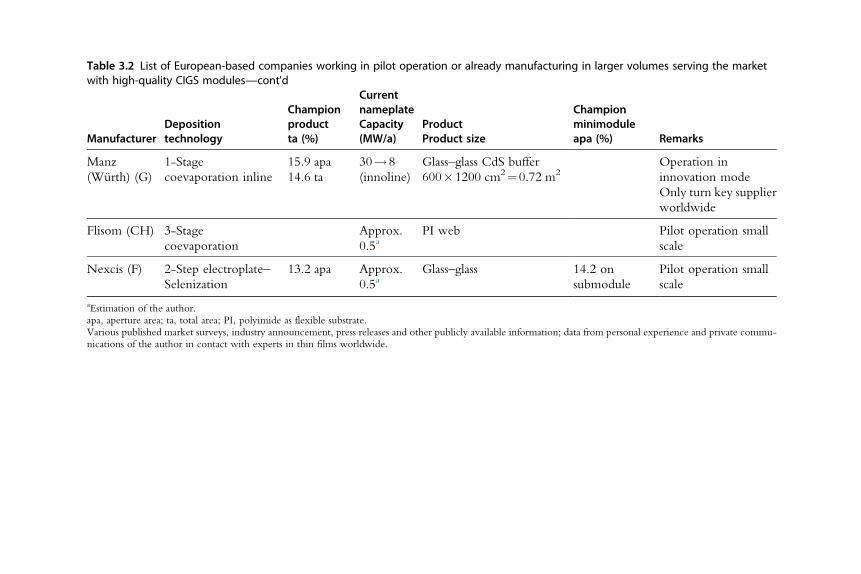
Table 3.2 List of European-based companies working in pilot operation or already manufacturing in larger volumes serving the marketwith high-quality CIGS modules—cont'd
ManufacturerDepositiontechnology
Championproductta (%)
CurrentnameplateCapacity(MW/a)
ProductProduct size
Championminimoduleapa (%) Remarks
Manz
(Wurth) (G)
1-Stage
coevaporation inline
15.9 apa
14.6 ta
30!8
(innoline)
Glass–glass CdS buffer
600�1200 cm2¼0.72 m2Operation in
innovation mode
Only turn key supplier
worldwide
Flisom (CH) 3-Stage
coevaporation
Approx.
0.5aPI web Pilot operation small
scale
Nexcis (F) 2-Step electroplate–
Selenization
13.2 apa Approx.
0.5aGlass–glass 14.2 on
submodule
Pilot operation small
scale
aEstimation of the author.apa, aperture area; ta, total area; PI, polyimide as flexible substrate.Various published market surveys, industry announcement, press releases and other publicly available information; data from personal experience and private commu-nications of the author in contact with experts in thin films worldwide.

Table 3.3 List of US- and Asian-based companies working in pilot operation or already manufacturing in larger volumes servingthe market with high-quality CIGS modules
ManufacturerDepositiontechnology
Championproductta (%)
CurrentnameplateCapacity(MW/a)
ProductProduct size
Championminimoduleapa (%) Remarks
Solar
Frontier ( J)
2-Step: Sputter
+H2Se/H2S-
crystallization
14.6 1000 Glass–glass Cd-free buffer
977�1257 mm2¼1.22 m217.8 on
30�30 cm2
12.6 with
CZTS device
Announced for 2015:
new factory with
+150 MW/a
STION
(USA)
TSMC (TA)
2-Step: Sputter
+H2Se/H2S-
crystallization
14.5
15.7
75+5
pilota
100
Glass–glass CdS buffer
656�1656 mm2¼1.08 m223.2 Tandem
device
MiaSole
(USA)
Reactive sputter 15.7 apa 75a ss web, glass–glass, buffer
CdS sputter
665�1611 mm2¼1.07 m2
Overtaken by Hanergy/
China
Glass–glass module,
prototype flexible
Samsung
SDI (SK)
2-Step: Sputter
+H2Se/H2S-
crystallization
15.7 1a Glass–glass
900�1600 mm2¼1.44 m2CIGS process not clear
small pilot operation
Global Solar
Energy
(USA)
3-Stage
coevaporation
13 40a ss web, glass–glass Overtaken by Hanergy/
China
SIVA Power
(USA)
3-Stage
coevaporation
Glass Lab cell 18.8% Start up in CIGS, small,
rather lab
aEstimation of the author.apa, aperture area; ss, stainless steel flexible substrate.Various published market surveys, industry announcement, press releases, and other publicly available information; data from personal experience and private commu-nications of the author in contact with experts in thin films worldwide.Data from press releases of the companies, status May 2014.

Table 3.4 Companies producing CdTe in larger amounts
ManufacturerDepositiontechnology
Championproduct ta(%)
CurrentnameplateCapacity(MW/a)
ProductProduct size
Champion lab cellactive area (%) Remarks
First Solar
(USA)
Medium vacuum
thermal evaporation
17.0 Approx.
2200
Glass–glass
600�1.200 mm2¼0.72 m220.4 Global player
Production lines in
USA and Malaysia
Calyxo (G) Atmospheric
thermal evaporation
13.4 Approx.
80
Glass–glass
600�1.200 mm2¼0.72 m2
apa, aperture area.Various published market surveys, industry announcement, press releases and other publicly available information; data from personal experience and private commu-nications of the author in contact with experts in thin films worldwide.
Data from press releases of the companies, status May 2014.

technical, and economic progress that has to be realized mainly relies on
quality and productivity features. Overall, fabrication cost of the module
is the major prerequisite for being competitive. Finally, the cost of electricity
produced (LCoE, levelized cost of electricity) is the main driver of compet-
itiveness in the ambient of electricity production also with conventional
sources and other renewable energies. In Table 3.5, the necessary bench-
marks for the numbers to reach are collected.
The depicted data are estimations of the author which are realistic and
necessary to reach in order to stay competitive in the electricity market.
In the long-term champion cell efficiencies will go to 25% and above
whereas mean module efficiency can approach 20% in the long term. Min-
imum total manufacturing cost (CoO) is actually about 0.4€/Wp for
medium-sized production lines of about 150 MWp/a capacity and can be
reduced by another 30–40% with actually known techniques and materials;
finally, the costs are limited by today’s module design which is based on glass
laminates. Together with a cost decrease to be expected also on the BOS side
system cost can go down to a minimum of about 0.5€/Wp with TF mod-
ules. PV systems based on these estimations can come down to an LCoE of
about 5–6€/kWh in middle European climate conditions.
These numbers are optimistic and based on keeping and even enhancing
high-level R&D around the main companies. Collaborative R&D actions
should be decided even together with competitors joining forces to over-
come low market presence of today in competition with c-Si technology.
As bill of materials (material cost) of TF modules is about 50% of total
cost whereas capital expenditure (capex) is in the range of about 20–30%,
Table 3.5 Numbers to be reached in the short, medium, and long term for thin-filmPV champion cells and modules as well as cost of ownership (CoO), total system cost,and levelized cost of electricity (LCoE)
Lab cell eff. act.area (%)
Av. prod. moduleeff. ta (%)
CoO(€/W)
Systemcost (€/W)
LCoE in middleEurope (€/kWh)
Short term
5 a
23 16 0.35 <1 8
Medium
term
10 a
25 18 0.3 0.8 6
Long term
15–20 a
>25 20 0.25 0.6 5
133Overview of Thin-Film Solar Cell Technologies

these cost categories are most important to work on. Other costs of person-
nel are about 5% and electricity about 6–8% (database Manz AG).
Electricity will become an important factor due to overall sustainability
of PV in the longer term. Energy payback times for TF modules—equal for
all materials—are with large volume manufacturing already in the range of
about 8 months for middle European climate and with further improve-
ments in overall qualities that will remain a main advantage in comparison
to c-Si. For the energy payback time of c-Si wafer technology is it not pos-
sible to come down below the range of 18–24 months due to the high
energy consumption for material cleaning and crystallization.
Therefore, the main aspects in order to reduce fabrication costs and the
most important topics for R&D for TF in the future are mainly by reducing
• material cost by
• using less pure feedstock materials
• increasing material utilization during deposition
• reducing active layer thicknesses
• minimization of interconnection losses
• on-site glass production at high line capacities �500 MWp/a
• replacement of glass by cheap but highly transparent webs with high
barrier characteristics
• capex by improvements in
• throughput/tact time per unit per equipment
• process and manufacturing yield
• equipment availability/uptime
Module area will be increased for next-generation TF PVmodules up to the
order of 1.5–2 m2 by next generation and standardization of equipment;
throughput will be increased by a factor of 5–10 in comparison to today.
Higher maturity of equipment and more professional operation will opti-
mize production yields and availability.
As it is clear for TF PV technology, there are still high cost reduction and
quality improvement potentials not yet applied to large volume production
lines; so to say that TF technology with first large volume manufacturing of
only two main players as First Solar for CdTe and Solar Frontier for CIGS is
just entering the learning curve which is of the order of about 20% lower
than c-Si productions. The shape of the learning curve will be steeper
due to implementation of upgrades in production lines in a professional
way during at least the next 10–20 years.
TF PV has the chance to become the main player in PV materials.
In order to reach that level, some aspects to follow are listed in the following:
134 Bernhard Dimmler

• acceleration of transfer results and know-how from lab to fab; more
focused lab R&D to manufacturing needs and conditions with a closer
link of laboratories to factories and setting priorities including more col-
laborative work to accelerate development by joining forces
• topics in fundamental R&D:
• better understanding of device physics, improving device quality
• long-term replacement of scarce and high cost elements like indium
or tellurium
• improved material quality, reduced thickness, gradient, and band gap
modifications (esp. with CIGS with, e.g., Ga content up)
• improvement and modifications of contact and buffer layers to
increase overall absorption and to enhance the useful portion of
the light spectrum
• optimization of contacts to reduce carrier losses
• use of novel or modified materials, multispectral devices (tandem and
triple band gap devices), up- and down conversion layers, improve-
ment of optics by reducing reflectivity and parasitic light absorption
in TCO layers
• use of combinations with organic layers and c-Si materials
• applied R&D:
• reduction of interconnect and module edge areas
• modification of patterning techniques, combination of laser scribing
with printing techniques
• other interconnect schemes, combination of scribing, printing, and
bus bars
• all back contact devices
• other glasses than soda lime sheet glass, speciality glasses (higher soft-
ening temperature, higher strength, lower thickness, and weight)
• flexible and thin substrate like stainless steel or PI webs of very thin,
flexible speciality glasses
• high isolation barrier coatings to avoid second glass lamination
• nonvacuum, atmospheric pressure deposition techniques like
printing, etc.
• introduction and prequalification of new inline metrology tools
• modifications of devices for further reduction of temperature
coefficients
• improvement of device quality, sealing components, and materials to
enhance stable operation beyond 30 years
• environmentally sustainable materials and recycling issues
135Overview of Thin-Film Solar Cell Technologies

• industrial R&D, introduction of prequalified materials and processes:
• increase of module efficiency and stability, introducing results from
laboratory to volume production
• increase of throughput by higher deposition rates and shorter heating
and cooling cycles
• next-generation equipment for bigger substrate sizes
• improvement of factory layouts and logistics applying, e.g., automo-
tive and semiconductor concepts to increase factory yield and
availability
• integration of better metrology tools for quality assurance
• standardization of equipment, materials, and components
• minimization of energy needed for materials and production
This list of topics is for sure not complete; nevertheless, it covers the main
features for future improvement for competiveness in the PV market. The
key and decisive factor is scaling to high volumes in order to profit from cost
reductions by reduction of capital expenditure of equipment and infrastruc-
ture and by purchasing high quantities of materials at lower cost.
Fulfilling these tasks and aspects for continuous improvement of module
qualities and manufacturing productivity to reduce cost of modules together
with a reduction in BOS, TF PVmaterials have a good chance getting bigger
in size and market share and becoming even more competitive in the long-
time frame. There are still a lot of potentials to gain, but there has to be
developed the right industrial strategy supported by an adequate industry
policy.
REFERENCESEPIA, 2014. Global Market Outlook 2014–2018. EPIA, Intersolar, Munich.Green, M.A., Emery, K., Hishikawa, Y., Warta, W., Dunlop, E.D., 2014. Solar cell effi-
ciency tables (version 43). Prog. Photovolt. Res. Appl. 22, 1–9.Manz AG. Data from Manz internal CIGS database. Reutlingen, Germany.SPVMarket Research, 2014. PhotovoltaicManufacturer Shipments: Capacity, Price &Rev-
enues 2013/2014: Report SPV-Supply2, SPV Market Research, April 2014, PaulaMints.
136 Bernhard Dimmler
INDEX
Note: Page numbers followed by “f ” indicate figures and “t” indicate tables.
AAmphoteric defect, 78–79
a-Si:H. See Hydrogenated amorphous
silicon (a-Si:H)
Atmospheric pressure chemical vapor
deposition (APCVD), 27
Auger recombination, 15–16
BBack surface field (BSF), 9
Boron-doped a-Si:H film, 85, 86
Building-integrated photovoltaics (BIPV),
102–103
CCalyxo, 128
Carrier recombination, silicon
defect recombination, 74, 75, 78–79, 95
intrinsic recombination, 74, 75–76
CdTe, 121–123
cell efficiency research, 126–128
First Solar, 124, 128
large volume manufacturing, 134
manufacturer, 132t
Chemical surface passivation, 75–76
CIGS. See Cu(In,Ga)(Se,S)2 (CIGS)
Continuous CZ pulling (CCZ), 100–102
Crystalline silicon (c-Si)
a-Si:H/c-Si heterojunction solar cells
(see Silicon heterojunction solar cells)
defect recombination, 75
industrial c-Si solar cell (see Industrial
crystalline Si (c-Si) solar cell)
passivating contacts, 75–76
TF PV materials, 121–123
energy payback time, 134
large volume production lines, 134
R&D work, 125–126
turnkey solutions, 124
Cu(In,Ga)(Se,S)2 (CIGS), 121–123
cell efficiency research, 126–128
European-based companies, 129t
First Solar, 128
large volume manufacturing, 134
Solar Frontier, 124, 128
US- and Asian-based companies, 131t
DDeep-defect recombination, 78–79
Diffused-junction solar cells
best cells, 92, 94t
cell current–voltage characteristics, 106
diffused emitter, 86–87
metallization, 90–92
p-doped c-Si, 82–83
production costs, 107
temperature coefficient, 102–103
Doped a-Si:H films
carrier selective contacts, 85
cross-contamination, 86
molybdenum oxide (MoOx), 86
PECVD, 86
EEdge-defined film-fed growth (EFG), 8
Ethylene vinyl acetate (EVA), 49, 49f, 50f
FField-effect passivation, 75
Fill factor (FF) losses, 95–96
First Solar, 124, 128
HHeterojunction with intrinsic thin layer
(HIT) concept, 6–7, 39–40
Honeymoon cell, 76–77
Hydrogenated amorphous silicon (a-Si:H)
as-deposited polycrystalline layers, 80–81
carrier recombination, 78–79
doped a-Si:H films
carrier selective contacts, 85
cross-contamination, 86
molybdenum oxide (MoOx), 86
PECVD, 86
137

Hydrogenated amorphous silicon (a-Si:H)
(Continued )
epitaxial growth, 81
honeymoon cell, 76–77
H2 plasma treatments, 81–82, 82f
isothermal annealing, 79
mechanism, 79
n- and p-type wafers, 82–83
Panasonic, 77–78
PECVD, 79–80, 104–105, 105f
planar deposition technology, 76–77
solar cell efficiency, 76–78, 102–103
TCO layers (see Transparent conductive
oxide (TCO) layers)
IIBC solar cells. See Interdigitated-back-
contacted (IBC) solar cells
Indium tin oxide (ITO), 88–89
absorbance spectra, 90f
external quantum efficiency and
1-reflectance spectra, 90f
thickness, mobility and free-electron
density, 89f
Industrial crystalline Si (c-Si) solar cell
alkaline wafer texturing, 35
Auger recombination, 15–16
band diagram, 10–12, 11f
basic structure of, 9–10, 9f
complex processing scheme, 5
cost reduction, 5–7
1-diode model, 12
efficiency of, 5
emitter formation
homogeneous emitters, 41–42, 42f
selective emitters (see Selective emitter
(SE))
firing through SiNx:H process
edge isolation, 25
inline/batch processing, 19
P diffusion, 22–25, 23f
screen-printing metallization
(see Screen printing)
SiNx:H deposition, 25–27
wafer washing, texturization, and
cleaning, 20–22, 21f
front contact metallization
dispensing, 37–38
double print, 36
drawbacks and challenges, 35–36
dual print, 36
multi-busbar approaches, 39–40
paste development, 38
seed-and-plate, 38–39
stencil printing, 36–37, 37f
fundamental loss mechanisms, 13–14, 13f
heterojunction emitter technology, 61
IBC-HIT approach, 6–7
j–V characteristics, 12–13, 12f, 33–34
n-type Si wafers, 61
optical and electrical losses, 18, 19f
output power, 12–13, 12f
PERC-type solar cells (see Passivated
emitter and rear cell (PERC))
PERL, 51, 52f
PERT, 51, 52f
photovoltaic (PV)
German PV market, 7–8
market share of, 8, 8f
solar modules, yearly production/
shipment of, 7–8, 7f
in space/terrestrial applications, 4–5
wafer and module costs, 9, 10f
radiative recombination, 14–15
rear contacted solar cells, 61
saturation current density, 18
SRH recombination, 16–17
surface recombination, 17
two-diode model, 14, 14f
wafer sawing, 34–35
Interdigitated-back-contacted (IBC) solar
cells, 6–7, 92–95, 94t
Intrinsic recombination, 74, 75–76
LLaser fired contacts (LFC), 54
MMolybdenum oxide (MoOx), 86
Monocrystalline Si (mono-Si), 6
Multicrystalline Si (mc-Si), 6
OOpen-circuit voltage (Voc) losses, 95
PPassivated emitter and rear cell (PERC)
boron–oxygen related degradation
138 Index

metastable, 57
regenerated state, 58–59, 59f
strategies, 57–58
dielectric rear side passivation
Al2O3 layers, 53
Al2O3/SiNx:H stacks, 53–54
SiO2/SiNx:H stacks, 54
efficiencies of, 59–60
local rear contact formation
contact patterns and void formation,
55–56
etching paste, 55
interconnection ribbons, soldering of,
56–57
laser fired contacts, 54
local ablation, 55
Phosphor silicate glass (PSG), 22
Phosphorus-doped a-Si:H film, 85, 86
Plasma-enhanced chemical vapor deposition
(PECVD), 26–27, 79–80, 86,
104–105, 105f
SScreen printing, 28f, 90–92, 103
co-firing step, 32–33, 33f
front side metallization, 28–29, 30f
inline process, 27–28
lifetime of, 27–28
rear side metallization, 29–32, 31f
Seed-and-plate approach, 38–39
Selective emitter (SE)
buried contact approach, 43
doped Si inks, 44
efficiency potential of, 50–51
etch-back process, 45–48, 45f, 46f, 47f
EVA and silicone, encapsulation, 49–50,
49f, 50f
ion implantation process, 44–45
laser doping
laser chemical processing, 48
NiAg light-induced plating, 48
P-glass, 48
and plating, 48
oxide mask process, 44, 44f
restrictions, 43
Shockley–Read–Hall recombination
statistics, 16–17, 78–79
Short-circuit current density ( Jsc) losses
blue absorption, 98
full silver reflector, 97, 97f
infrared parasitic absorption, 98–99
Lambertian surfaces, 99
recombination losses, 96–97
reflection losses, 96–97
Silicon
carrier recombination
defect recombination, 74, 75, 78–79, 95
intrinsic recombination, 74, 75–76
emitter diffusion process, 74
Silicon dangling bond, 78–79
Silicon heterojunction solar cells
a-Si:H, surface passivation
as-deposited polycrystalline layers,
80–81
carrier recombination, 78–79
epitaxial growth, 81
honeymoon cell, 76–77
H2 plasma treatments, 81–82, 82f
isothermal annealing, 79
mechanism, 79
n- and p-type wafers, 82–83
Panasonic, 77–78
PECVD, 79–80, 104–105, 105f
planar deposition technology, 76–77
solar cell efficiency, 76–78, 102–103
band diagram, 77–78, 78f
CEAINES, 99–100
cell current–voltage characteristics, 106
challenges, 108–109, 109t
chemical surface passivation, 76
Choshu Industry, 99–100
curing process, 106
current annual production capacities,
99–100
deposited emitter, 86–87
device configurations, 103–104
efficiency vs. bulk lifetime, 100–102, 101f
electron and hole collectors, 85–86
energy yield, 102–103
fill factor (FF) losses, 95–96
front TCO layers, 86–87, 105–106
IBC solar cells, 92–95, 94t
low-temperature copper paste, 91
low-temperature soldering, 103
material requirements, 100–102
minority-carrier effective lifetimes, 84f
monocrystalline silicon CZ wafer, 83–85
multi-wire contacting scheme, 91, 91f
139Index

Silicon heterojunction solar cells (Continued )
open-circuit voltage (Voc) losses, 95
opportunities, 109t
parallel-plate PECVD, 104
PC1D simulations, 100–102, 101f, 102f
plated contacts, 92, 103
production costs, 107–108
random-pyramid texturing, 83–85
rear TCO layers, 87–88, 105–106
research activities, 99–100
Sanyo patents, 99–100
screen printing, 90–92, 103
short-circuit current density ( Jsc) losses
blue absorption, 98
full silver reflector, 97, 97f
infrared parasitic absorption, 98–99
Lambertian surfaces, 99
recombination losses, 96–97
reflection losses, 96–97
Silevo, 99–100
strengths, 108–109, 109t
Sunpreme, 99–100
temperature coefficient, 102–103
thin-film deposition technology, 76
vs. silicon homojunction solar cell
technology, 76–77
wafer cleaning and texturing, 85, 104
wafer doping density vs. efficiency,
100–102, 102f
wet chemistry, 104
Solar Frontier, 128
Stencil printing, 36–37, 37f
Surface passivation, silicon heterojunction
solar cells
as-deposited polycrystalline layers, 80–81
carrier recombination, 78–79
epitaxial growth, 81
honeymoon cell, 76–77
H2 plasma treatments, 81–82, 82f
isothermal annealing, 79
mechanism, 79
n- and p-type wafers, 82–83
Panasonic, 77–78
PECVD, 79–80, 104–105, 105f
planar deposition technology, 76–77
solar cell efficiency, 76–78, 102–103
TThin-film photovoltaic (TF PV) modules
applied R&D, 135
Calyxo, 128
capital expenditure, 133–134
CdTe (see CdTe)
cell efficiency, 125–128, 126f
CIGS (see Cu(In,Ga)(Se,S)2 (CIGS))
collaborative R&D actions, 133
cost of ownership (CoO), 133, 133t
c-Si (see Crystalline silicon (c-Si))
energy payback time, 134
First Solar, 128
full-size module champion, 127t
fundamental R&D, 135
grid parity, 123
industrial R&D, 136
large volume production lines, 134
levelized cost of electricity, 128–133,
133t
long-term champion companies, cost
estimations of, 128–133
market share, 121–125
material cost, 133–134
minimodule champion, 127t
module area and throughput, 134
shipped modules vs. year, 125f
small-cell module champion, 127t
Solar Frontier, 128
total system cost, 133, 133t
turnkey solutions, 124
worldwide shipments, 123f
Transparent conductive oxide (TCO) layers
front layers, 86–87, 105–106
ITO and IO:H layer, 88–89
absorbance spectra, 90f
external quantum efficiency and
1-reflectance spectra, 90f
thickness, mobility and free-electron
density, 89f
rear layers, 87–88, 105–106
Two-diode model, 14, 14f
UUpgraded metallurgical grade (UMG), 5–6
140 Index

CONTENTS OF VOLUMES IN THIS SERIES
Volume 1 Physics of III–V Compounds
C. Hilsum, Some Key Features of III–V Compounds
F. Bassani, Methods of Band Calculations Applicable to III–V Compounds
E. O. Kane, The k-p Method
V. L. Bonch–Bruevich, Effect of Heavy Doping on the Semiconductor Band Structure
D. Long, Energy Band Structures of Mixed Crystals of III–V Compounds
L. M. Roth and P. N. Argyres, Magnetic Quantum Effects
S. M. Puri and T. H. Geballe, Thermomagnetic Effects in the Quantum Region
W. M. Becker, Band Characteristics near Principal Minima from Magnetoresistance
E. H. Putley, Freeze-Out Effects, Hot Electron Effects, and Submillimeter Photoconductivity in InSb
H. Weiss, Magnetoresistance
B. Ancker-Johnson, Plasma in Semiconductors and Semimetals
Volume 2 Physics of III–V Compounds
M. G. Holland, Thermal Conductivity
S. I. Novkova, Thermal Expansion
U. Piesbergen, Heat Capacity and Debye Temperatures
G. Giesecke, Lattice Constants
J. R. Drabble, Elastic Properties
A. U. Mac Rae and G. W. Gobeli, Low Energy Electron Diffraction Studies
R. Lee Mieher, Nuclear Magnetic Resonance
B. Goldstein, Electron Paramagnetic Resonance
T. S. Moss, Photoconduction in III–V Compounds
E. Antoncik and J. Tauc, Quantum Efficiency of the Internal Photoelectric Effect in InSb
G. W. Gobeli and I. G. Allen, Photoelectric Threshold and Work Function
P. S. Pershan, Nonlinear Optics in III–V Compounds
M. Gershenzon, Radiative Recombination in the III–V Compounds
F. Stern, Stimulated Emission in Semiconductors
Volume 3 Optical Properties of III–V Compounds
M. Hass, Lattice Reflection
W. G. Spitzer, Multiphonon Lattice Absorption
D. L. Stierwalt and R. F. Potter, Emittance Studies
H. R. Philipp and H. Ehrenveich, Ultraviolet Optical Properties
M. Cardona, Optical Absorption Above the Fundamental Edge
E. J. Johnson, Absorption Near the Fundamental Edge
J. O. Dimmock, Introduction to the Theory of Exciton States in Semiconductors
141
B. Lax and J. G. Mavroides, Interband Magnetooptical Effects
H. Y. Fan, Effects of Free Carries on Optical Properties
E. D. Palik and G. B. Wright, Free-Carrier Magnetooptical Effects
R. H. Bube, Photoelectronic Analysis
B. O. Seraphin and H. E. Benett, Optical Constants
Volume 4 Physics of III–V Compounds
N. A. Goryunova, A. S. Borchevskii and D. N. Tretiakov, Hardness
N. N. Sirota, Heats of Formation and Temperatures and Heats of Fusion of Compounds of AIIIBV
D. L. Kendall, Diffusion
A. G. Chynoweth, Charge Multiplication Phenomena
R. W. Keyes, The Effects of Hydrostatic Pressure on the Properties of III–V Semiconductors
L. W. Aukerman, Radiation Effects
N. A. Goryunova, F. P. Kesamanly, and D. N. Nasledov, Phenomena in Solid Solutions
R. T. Bate, Electrical Properties of Nonuniform Crystals
Volume 5 Infrared Detectors
H. Levinstein, Characterization of Infrared Detectors
P. W. Kruse, Indium Antimonide Photoconductive and Photoelectromagnetic Detectors
M. B. Prince, Narrowband Self-Filtering Detectors
I. Melngalis and T. C. Hannan, Single-Crystal Lead-Tin Chalcogenides
D. Long and J. L. Schmidt, Mercury-Cadmium Telluride and Closely Related Alloys
E. H. Putley, The Pyroelectric Detector
N. B. Stevens, Radiation Thermopiles
R. J. Keyes and T. M. Quist, Low Level Coherent and Incoherent Detection in the Infrared
M. C. Teich, Coherent Detection in the Infrared
F. R. Arams, E. W. Sard, B. J. Peyton and F. P. Pace, Infrared Heterodyne Detection with Gigahertz IF
Response
H. S. Sommers, Jr., Macrowave-Based Photoconductive Detector
R. Sehr and R. Zuleeg, Imaging and Display
Volume 6 Injection Phenomena
M. A. Lampert and R. B. Schilling, Current Injection in Solids: The Regional Approximation Method
R. Williams, Injection by Internal Photoemission
A. M. Barnett, Current Filament Formation
R. Baron and J. W. Mayer, Double Injection in Semiconductors
W. Ruppel, The Photoconductor-Metal Contact
142 Contents of Volumes in this Series

Volume 7 Application and Devices
Part A
J. A. Copeland and S. Knight, Applications Utilizing Bulk Negative Resistance
F. A. Padovani, The Voltage-Current Characteristics of Metal-Semiconductor Contacts
P. L. Hower, W. W. Hooper, B. R. Cairns, R. D. Fairman, and D. A. Tremere, The GaAs Field-Effect
Transistor
M. H. White, MOS Transistors
G. R. Antell, Gallium Arsenide Transistors
T. L. Tansley, Heterojunction Properties
Part B
T. Misawa, IMPATT Diodes
H. C. Okean, Tunnel Diodes
R. B. Campbell and Hung-Chi Chang, Silicon Junction Carbide Devices
R. E. Enstrom, H. Kressel, and L. Krassner, High-Temperature Power Rectifiers of GaAs1�xPx
Volume 8 Transport and Optical Phenomena
R. J. Stirn, Band Structure and Galvanomagnetic Effects in III–V Compounds with Indirect Band Gaps
R. W. Ure, Jr., Thermoelectric Effects in III–V Compounds
H. Piller, Faraday Rotation
H. Barry Bebb and E. W. Williams, Photoluminescence I: Theory
E. W. Williams and H. Barry Bebb, Photoluminescence II: Gallium Arsenide
Volume 9 Modulation Techniques
B. O. Seraphin, Electroreflectance
R. L. Aggarwal, Modulated Interband Magnetooptics
D. F. Blossey and Paul Handler, Electroabsorption
B. Batz, Thermal and Wavelength Modulation Spectroscopy
I. Balslev, Piezooptical Effects
D. E. Aspnes and N. Bottka, Electric-Field Effects on the Dielectric Function of Semiconductors and
Insulators
Volume 10 Transport Phenomena
R. L. Rhode, Low-Field Electron Transport
J. D. Wiley, Mobility of Holes in III–V Compounds
C. M. Wolfe and G. E. Stillman, Apparent Mobility Enhancement in Inhomogeneous Crystals
R. L. Petersen, The Magnetophonon Effect
143Contents of Volumes in this Series

Volume 11 Solar Cells
H. J. Hovel, Introduction; Carrier Collection, Spectral Response, and Photocurrent; Solar Cell Electrical
Characteristics; Efficiency; Thickness; Other Solar Cell Devices; Radiation Effects; Temperature
and Intensity; Solar Cell Technology
Volume 12 Infrared Detectors (II)
W. L. Eiseman, J. D. Merriam, and R. F. Potter, Operational Characteristics of Infrared Photodetectors
P. R. Bratt, Impurity Germanium and Silicon Infrared Detectors
E. H. Putley, InSb Submillimeter Photoconductive Detectors
G. E. Stillman, C. M. Wolfe, and J. O. Dimmock, Far-Infrared Photoconductivity in High Purity GaAs
G. E. Stillman and C. M. Wolfe, Avalanche Photodiodes
P. L. Richards, The Josephson Junction as a Detector of Microwave and Far-Infrared Radiation
E. H. Putley, The Pyroelectric Detector – An Update
Volume 13 Cadmium Telluride
K. Zanio, Materials Preparations; Physics; Defects; Applications
Volume 14 Lasers, Junctions, Transport
N. Holonyak, Jr., and M. H. Lee, Photopumped III–V Semiconductor Lasers
H. Kressel and J. K. Butler, Heterojunction Laser Diodes
A. Van der Ziel, Space-Charge-Limited Solid-State Diodes
P. J. Price, Monte Carlo Calculation of Electron Transport in Solids
Volume 15 Contacts, Junctions, Emitters
B. L. Sharma, Ohmic Contacts to III–V Compounds Semiconductors
A. Nussbaum, The Theory of Semiconducting Junctions
J. S. Escher, NEA Semiconductor Photoemitters
Volume 16 Defects, (HgCd)Se, (HgCd)Te
H. Kressel, The Effect of Crystal Defects on Optoelectronic Devices
C. R.Whitsett, J. G. Broerman, and C. J. Summers, Crystal Growth and Properties of Hg1�xCdx Se Alloys
M. H. Weiler, Magnetooptical Properties of Hg1�x Cdx Te Alloys
P. W. Kruse and J. G. Ready, Nonlinear Optical Effects in Hg1�x Cdx Te
Volume 17 CW Processing of Silicon and Other Semiconductors
J. F. Gibbons, Beam Processing of Silicon
A. Lietoila, R. B. Gold, J. F. Gibbons, and L. A. Christel, Temperature Distributions and Solid Phase
Reaction Rates Produced by Scanning CW Beams
144 Contents of Volumes in this Series

A. Leitoila and J. F. Gibbons, Applications of CW Beam Processing to Ion Implanted Crystalline Silicon
N. M. Johnson, Electronic Defects in CW Transient Thermal Processed Silicon
K. F. Lee, T. J. Stultz, and J. F. Gibbons, Beam Recrystallized Polycrystalline Silicon: Properties,
Applications, and Techniques
T. Shibata, A. Wakita, T. W. Sigmon and J. F. Gibbons, Metal-Silicon Reactions and Silicide
Y. I. Nissim and J. F. Gibbons, CW Beam Processing of Gallium Arsenide
Volume 18 Mercury Cadmium Telluride
P. W. Kruse, The Emergence of (Hg1�x Cdx) Te as a Modern Infrared Sensitive Material
H. E. Hirsch, S. C. Liang, and A. G. White, Preparation of High-Purity Cadmium, Mercury, and
Tellurium
W. F. H. Micklethwaite, The Crystal Growth of Cadmium Mercury Telluride
P. E. Petersen, Auger Recombination in Mercury Cadmium Telluride
R. M. Broudy and V. J. Mazurczyck, (HgCd) Te Photoconductive Detectors
M. B. Reine, A. K. Soad, and T. J. Tredwell, Photovoltaic Infrared Detectors
M. A. Kinch, Metal-Insulator-Semiconductor Infrared Detectors
Volume 19 Deep Levels, GaAs, Alloys, Photochemistry
G. F. Neumark and K. Kosai, Deep Levels in Wide Band-Gap III–V Semiconductors
D. C. Look, The Electrical and Photoelectronic Properties of Semi-Insulating GaAs
R. F. Brebrick, Ching-Hua Su, and Pok-Kai Liao, Associated SolutionModel for Ga-In-Sb and Hg-Cd-Te
Y. Ya. Gurevich and Y. V. Pleskon, Photoelectrochemistry of Semiconductors
Volume 20 Semi-Insulating GaAs
R. N. Thomas, H. M. Hobgood, G. W. Eldridge, D. L. Barrett, T. T. Braggins, L. B. Ta, and S. K. Wang,
High-Purity LEC Growth and Direct Implantation of GaAs for Monolithic Microwave Circuits
C. A. Stolte, Ion Implantation and Materials for GaAs Integrated Circuits
C. G. Kirkpatrick, R. T. Chen, D. E. Holmes, P. M. Asbeck, K. R. Elliott, R. D. Fairman, and J. R. Oliver,
LEC GaAs for Integrated Circuit Applications
J. S. Blakemore and S. Rahimi, Models for Mid-Gap Centers in Gallium Arsenide
Volume 21 Hydrogenated Amorphous Silicon
Part A
J. I. Pankove, Introduction
M. Hirose, Glow Discharge; Chemical Vapor Deposition
Y. Uchida, di Glow Discharge
T. D. Moustakas, Sputtering
I. Yamada, Ionized-Cluster Beam Deposition
B. A. Scott, Homogeneous Chemical Vapor Deposition
145Contents of Volumes in this Series
F. J. Kampas, Chemical Reactions in Plasma Deposition
P. A. Longeway, Plasma Kinetics
H. A. Weakliem, Diagnostics of Silane Glow Discharges Using Probes and Mass Spectroscopy
L. Gluttman, Relation between the Atomic and the Electronic Structures
A. Chenevas-Paule, Experiment Determination of Structure
S. Minomura, Pressure Effects on the Local Atomic Structure
D. Adler, Defects and Density of Localized States
Part B
J. I. Pankove, Introduction
G. D. Cody, The Optical Absorption Edge of a-Si: H
N. M. Amer and W. B. Jackson, Optical Properties of Defect States in a-Si: H
P. J. Zanzucchi, The Vibrational Spectra of a-Si: H
Y. Hamakawa, Electroreflectance and Electroabsorption
J. S. Lannin, Raman Scattering of Amorphous Si, Ge, and Their Alloys
R. A. Street, Luminescence in a-Si: H
R. S. Crandall, Photoconductivity
J. Tauc, Time-Resolved Spectroscopy of Electronic Relaxation Processes
P. E. Vanier, IR-Induced Quenching and Enhancement of Photoconductivity and Photoluminescence
H. Schade, Irradiation-Induced Metastable Effects
L. Ley, Photoelectron Emission Studies
Part C
J. I. Pankove, Introduction
J. D. Cohen, Density of States from Junction Measurements in Hydrogenated Amorphous Silicon
P. C. Taylor, Magnetic Resonance Measurements in a-Si: H
K. Morigaki, Optically Detected Magnetic Resonance
J. Dresner, Carrier Mobility in a-Si: H
T. Tiedje, Information About Band-Tail States from Time-of-Flight Experiments
A. R. Moore, Diffusion Length in Undoped a-S: H
W. Beyer and J. Overhof, Doping Effects in a-Si: H
H. Fritzche, Electronic Properties of Surfaces in a-Si: H
C. R. Wronski, The Staebler-Wronski Effect
R. J. Nemanich, Schottky Barriers on a-Si: H
B. Abeles and T. Tiedje, Amorphous Semiconductor Superlattices
Part D
J. I. Pankove, Introduction
D. E. Carlson, Solar Cells
G. A. Swartz, Closed-Form Solution of I–V Characteristic for a s-Si: H Solar Cells
I. Shimizu, Electrophotography
S. Ishioka, Image Pickup Tubes
P. G. Lecomber and W. E. Spear, The Development of the a-Si: H Field-Effect Transistor and its Possible
Applications
146 Contents of Volumes in this Series

D. G. Ast, a-Si: H FET-Addressed LCD Panel
S. Kaneko, Solid-State Image Sensor
M. Matsumura, Charge-Coupled Devices
M. A. Bosch, Optical Recording
A. D’Amico and G. Fortunato, Ambient Sensors
H. Kulkimoto, Amorphous Light-Emitting Devices
R. J. Phelan, Jr., Fast Decorators and Modulators
J. I. Pankove, Hybrid Structures
P. G. LeComber, A. E. Owen,W. E. Spear, J. Hajto, andW. K. Choi, Electronic Switching in Amorphous
Silicon Junction Devices
Volume 22 Lightwave Communications Technology
Part A
K. Nakajima, The Liquid-Phase Epitaxial Growth of InGaAsP
W. T. Tsang, Molecular Beam Epitaxy for III–V Compound Semiconductors
G. B. Stringfellow, Organometallic Vapor-Phase Epitaxial Growth of III–V Semiconductors
G. Beuchet, Halide and Chloride Transport Vapor-Phase Deposition of InGaAsP and GaAs
M. Razeghi, Low-Pressure, Metallo-Organic Chemical Vapor Deposition of GaxIn1�xAsP1�y Alloys
P. M. Petroff, Defects in III–V Compound Semiconductors
Part B
J. P. van der Ziel, Mode Locking of Semiconductor Lasers
K. Y. Lau and A. Yariv, High-Frequency Current Modulation of Semiconductor Injection Lasers
C. H. Henry, Special Properties of Semi Conductor Lasers
Y. Suematsu, K. Kishino, S. Arai, and F. Koyama, Dynamic Single-Mode Semiconductor Lasers with a
Distributed Reflector
W. T. Tsang, The Cleaved-Coupled-Cavity (C3) Laser
Part C
R. J. Nelson and N. K. Dutta, Review of InGaAsP InP Laser Structures and Comparison of Their
Performance
N. Chinone and M. Nakamura, Mode-Stabilized Semiconductor Lasers for 0.7–0.8- and 1.1–1.6-μmRegions
Y. Horikoshi, Semiconductor Lasers with Wavelengths Exceeding 2 μmB. A. Dean and M. Dixon, The Functional Reliability of Semiconductor Lasers as Optical Transmitters
R. H. Saul, T. P. Lee, and C. A. Burus, Light-Emitting Device Design
C. L. Zipfel, Light-Emitting Diode-Reliability
T. P. Lee and T. Li, LED-Based Multimode Lightwave Systems
K. Ogawa, Semiconductor Noise-Mode Partition Noise
Part D
F. Capasso, The Physics of Avalanche Photodiodes
T. P. Pearsall and M. A. Pollack, Compound Semiconductor Photodiodes
147Contents of Volumes in this Series
T. Kaneda, Silicon and Germanium Avalanche Photodiodes
S. R. Forrest, Sensitivity of Avalanche Photodetector Receivers for High-Bit-Rate
Long-Wavelength Optical Communication Systems
J. C. Campbell, Phototransistors for Lightwave Communications
Part E
S. Wang, Principles and Characteristics of Integrable Active and Passive Optical Devices
S. Margalit and A. Yariv, Integrated Electronic and Photonic Devices
T. Mukai, A. Yamamoto, and T. Kimura, Optical Amplification by Semiconductor Lasers
Volume 23 Pulsed Laser Processing of Semiconductors
R. F. Wood, C. W. White and R. T. Young, Laser Processing of Semiconductors: An Overview
C. W. White, Segregation, Solute Trapping and Supersaturated Alloys
G. E. Jellison, Jr., Optical and Electrical Properties of Pulsed Laser-Annealed Silicon
R. F. Wood and G. E. Jellison, Jr., Melting Model of Pulsed Laser Processing
R. F. Wood and F. W. Young, Jr., Nonequilibrium Solidification Following Pulsed Laser Melting
D. H. Lawndes and G. E. Jellison, Jr., Time-Resolved Measurement During Pulsed Laser Irradiation of
Silicon
D. M. Zebner, Surface Studies of Pulsed Laser Irradiated Semiconductors
D. H. Lowndes, Pulsed Beam Processing of Gallium Arsenide
R. B. James, Pulsed CO2 Laser Annealing of Semiconductors
R. T. Young and R. F. Wood, Applications of Pulsed Laser Processing
Volume 24 Applications of Multiquantum Wells, Selective Doping, and
Superlattices
C. Weisbuch, Fundamental Properties of III–V Semiconductor Two-Dimensional Quantized Structures:
The Basis for Optical and Electronic Device Applications
H. Morkoc and H. Unlu, Factors Affecting the Performance of (Al,Ga)As/GaAs and (Al,Ga)As/InGaAs
Modulation-Doped Field-Effect Transistors: Microwave and Digital Applications
N. T. Linh, Two-Dimensional Electron Gas FETs: Microwave Applications
M. Abe et al., Ultra-High-Speed HEMT Integrated Circuits
D. S. Chemla, D. A. B. Miller and P. W. Smith, Nonlinear Optical Properties of Multiple QuantumWell
Structures for Optical Signal Processing
F. Capasso, Graded-Gap and Superlattice Devices by Band-Gap Engineering
W. T. Tsang, Quantum Confinement Heterostructure Semiconductor Lasers
G. C. Osbourn et al., Principles and Applications of Semiconductor Strained-Layer Superlattices
Volume 25 Diluted Magnetic Semiconductors
W. Giriat and J. K. Furdyna, Crystal Structure, Composition, and Materials Preparation of Diluted
Magnetic Semiconductors
148 Contents of Volumes in this Series

W.M. Becker, Band Structure andOptical Properties ofWide-Gap AII1�xMnxBIV Alloys at ZeroMagnetic
Field
S. Oseroff and P. H. Keesom, Magnetic Properties: Macroscopic Studies
T. Giebultowicz and T. M. Holden, Neutron Scattering Studies of theMagnetic Structure and Dynamics of
Diluted Magnetic Semiconductors
J. Kossut, Band Structure and Quantum Transport Phenomena in Narrow-Gap Diluted Magnetic
Semiconductors
C. Riquaux, Magnetooptical Properties of Large-Gap Diluted Magnetic Semiconductors
J. A. Gaj, Magnetooptical Properties of Large-Gap Diluted Magnetic Semiconductors
J. Mycielski, Shallow Acceptors in Diluted Magnetic Semiconductors: Splitting, Boil-off, Giant Negative
Magnetoresistance
A. K. Ramadas and R. Rodriquez, Raman Scattering in Diluted Magnetic Semiconductors
P. A. Wolff, Theory of Bound Magnetic Polarons in Semimagnetic Semiconductors
Volume 26 III–V Compound Semiconductors and Semiconductor
Properties of Superionic Materials
Z. Yuanxi, III–V Compounds
H. V. Winston, A. T. Hunter, H. Kimura, and R. E. Lee, InAs-Alloyed GaAs Substrates for Direct
Implantation
P. K. Bhattacharya and S. Dhar, Deep Levels in III–V Compound Semiconductors Grown by MBE
Y. Ya. Gurevich and A. K. Ivanov-Shits, Semiconductor Properties of Supersonic Materials
Volume 27 High Conducting Quasi-One-Dimensional Organic Crystals
E. M. Conwell, Introduction to Highly Conducting Quasi-One-Dimensional Organic Crystals
I. A. Howard, A Reference Guide to the Conducting Quasi-One-Dimensional Organic Molecular
Crystals
J. P. Pouqnet, Structural Instabilities
E. M. Conwell, Transport Properties
C. S. Jacobsen, Optical Properties
J. C. Scolt, Magnetic Properties
L. Zuppiroli, Irradiation Effects: Perfect Crystals and Real Crystals
Volume 28 Measurement of High-Speed Signals in Solid State Devices
J. Frey and D. Ioannou, Materials and Devices for High-Speed and Optoelectronic Applications
H. Schumacher and E. Strid, Electronic Wafer Probing Techniques
D. H. Auston, Picosecond Photoconductivity: High-Speed Measurements of Devices and Materials
J. A. Valdmanis, Electro-Optic Measurement Techniques for Picosecond Materials, Devices and
Integrated Circuits
J. M. Wiesenfeld and R. K. Jain, Direct Optical Probing of Integrated Circuits and High-Speed Devices
G. Plows, Electron-Beam Probing
A. M. Weiner and R. B. Marcus, Photoemissive Probing
149Contents of Volumes in this Series
Volume 29 Very High Speed Integrated Circuits: Gallium Arsenide LSI
M. Kuzuhara and T. Nazaki, Active Layer Formation by Ion Implantation
H. Hasimoto, Focused Ion Beam Implantation Technology
T. Nozaki and A. Higashisaka, Device Fabrication Process Technology
M. Ino and T. Takada, GaAs LSI Circuit Design
M. Hirayama, M. Ohmori, and K. Yamasaki, GaAs LSI Fabrication and Performance
Volume 30 Very High Speed Integrated Circuits: Heterostructure
H. Watanabe, T. Mizutani, and A. Usui, Fundamentals of Epitaxial Growth and Atomic Layer Epitaxy
S. Hiyamizu, Characteristics of Two-Dimensional Electron Gas in III–V Compound Heterostructures
Grown by MBE
T. Nakanisi, Metalorganic Vapor Phase Epitaxy for High-Quality Active Layers
T. Nimura, High Electron Mobility Transistor and LSI Applications
T. Sugeta and T. Ishibashi, Hetero-Bipolar Transistor and LSI Application
H. Matsuedo, T. Tanaka, and M. Nakamura, Optoelectronic Integrated Circuits
Volume 31 Indium Phosphide: Crystal Growth and Characterization
J. P. Farges, Growth of Discoloration-Free InP
M. J. McCollum and G. E. Stillman, High Purity InP Grown by Hydride Vapor Phase Epitaxy
I. Inada and T. Fukuda, Direct Synthesis and Growth of Indium Phosphide by the Liquid Phosphorous
Encapsulated Czochralski Method
O. Oda, K. Katagiri, K. Shinohara, S. Katsura, Y. Takahashi, K. Kainosho, K. Kohiro, and R. Hirano, InP
Crystal Growth, Substrate Preparation and Evaluation
K. Tada, M. Tatsumi, M. Morioka, T. Araki, and T. Kawase, InP Substrates: Production and Quality
Control
M. Razeghi, LP-MOCVD Growth, Characterization, and Application of InP Material
T. A. Kennedy and P. J. Lin-Chung, Stoichiometric Defects in InP
Volume 32 Strained-Layer Superlattices: Physics
T. P. Pearsall, Strained-Layer Superlattices
F. H. Pollack, Effects of Homogeneous Strain on the Electronic and Vibrational Levels in Semiconductors
J. Y. Marzin, J. M. Gerard, P. Voisin, and J. A. Brum, Optical Studies of Strained III–V Heterolayers
R. People and S. A. Jackson, Structurally Induced States from Strain and Confinement
M. Jaros, Microscopic Phenomena in Ordered Superlattices
Volume 33 Strained-Layer Superlattices: Material Science and
Technology
R. Hull and J. C. Bean, Principles and Concepts of Strained-Layer Epitaxy
150 Contents of Volumes in this Series

W. J. Shaff, P. J. Tasker, M. C. Foisy, and L. F. Eastman, Device Applications of Strained-Layer Epitaxy
S. T. Picraux, B. L. Doyle, and J. Y. Tsao, Structure and Characterization of Strained-Layer Superlattices
E. Kasper and F. Schaffer, Group IV Compounds
D. L. Martin, Molecular Beam Epitaxy of IV–VI Compounds Heterojunction
R. L. Gunshor, L. A. Kolodziejski, A. V. Nurmikko, and N. Otsuka, Molecular Beam Epitaxy of I–VI
Semiconductor Microstructures
Volume 34 Hydrogen in Semiconductors
J. I. Pankove and N. M. Johnson, Introduction to Hydrogen in Semiconductors
C. H. Seager, Hydrogenation Methods
J. I. Pankove, Hydrogenation of Defects in Crystalline Silicon
J. W. Corbett, P. Deak, U. V. Desnica, and S. J. Pearton, Hydrogen Passivation of Damage Centers in
Semiconductors
S. J. Pearton, Neutralization of Deep Levels in Silicon
J. I. Pankove, Neutralization of Shallow Acceptors in Silicon
N. M. Johnson, Neutralization of Donor Dopants and Formation of Hydrogen-Induced Defects in
n-Type Silicon
M. Stavola and S. J. Pearton, Vibrational Spectroscopy of Hydrogen-Related Defects in Silicon
A. D. Marwick, Hydrogen in Semiconductors: Ion Beam Techniques
C. Herring and N. M. Johnson, Hydrogen Migration and Solubility in Silicon
E. E. Haller, Hydrogen-Related Phenomena in Crystalline Germanium
J. Kakalios, Hydrogen Diffusion in Amorphous Silicon
J. Chevalier, B. Clerjaud, and B. Pajot, Neutralization of Defects and Dopants in III–V Semiconductors
G. G. DeLeo and W. B. Fowler, Computational Studies of Hydrogen-Containing Complexes in
Semiconductors
R. F. Kiefl and T. L. Estle, Muonium in Semiconductors
C. G. Van de Walle, Theory of Isolated Interstitial Hydrogen and Muonium in Crystalline
Semiconductors
Volume 35 Nanostructured Systems
M. Reed, Introduction
H. van Houten, C. W. J. Beenakker, and B. J. Wees, Quantum Point Contacts
G. Timp, When Does a Wire Become an Electron Waveguide?
M. Buttiker, The Quantum Hall Effects in Open Conductors
W. Hansen, J. P. Kotthaus, and U. Merkt, Electrons in Laterally Periodic Nanostructures
Volume 36 The Spectroscopy of Semiconductors
D. Heiman, Spectroscopy of Semiconductors at Low Temperatures and High Magnetic Fields
A. V. Nurmikko, Transient Spectroscopy by Ultrashort Laser Pulse Techniques
151Contents of Volumes in this Series

A. K. Ramdas and S. Rodriguez, Piezospectroscopy of Semiconductors
O. J. Glembocki and B. V. Shanabrook, Photoreflectance Spectroscopy of Microstructures
D. G. Seiler, C. L. Littler, and M. H. Wiler, One- and Two-Photon Magneto-Optical Spectroscopy of
InSb and Hg1�xCdx Te
Volume 37 The Mechanical Properties of Semiconductors
A.-B. Chen, A. Sher, and W. T. Yost, Elastic Constants and Related Properties of Semiconductor
Compounds and Their Alloys
D. R. Clarke, Fracture of Silicon and Other Semiconductors
H. Siethoff, The Plasticity of Elemental and Compound Semiconductors
S. Guruswamy, K. T. Faber, and J. P. Hirth, Mechanical Behavior of Compound Semiconductors
S. Mahajan, Deformation Behavior of Compound Semiconductors
J. P. Hirth, Injection of Dislocations into Strained Multilayer Structures
D. Kendall, C. B. Fleddermann, and K. J. Malloy, Critical Technologies for the Micromatching of Silicon
J. Matsuba and K. Mokuya, Processing and Semiconductor Thermoelastic Behavior
Volume 38 Imperfections in III/V Materials
U. Scherz and M. Scheffler, Density-Functional Theory of sp-Bonded Defects in III/V Semiconductors
M. Kaminska and E. R. Weber, E12 Defect in GaAs
D. C. Look, Defects Relevant for Compensation in Semi-Insulating GaAs
R. C. Newman, Local Vibrational Mode Spectroscopy of Defects in III/V Compounds
A. M. Hennel, Transition Metals in III/V Compounds
K. J. Malloy and K. Khachaturyan, DX and Related Defects in Semiconductors
V. Swaminathan and A. S. Jordan, Dislocations in III/V Compounds
K. W. Nauka, Deep Level Defects in the Epitaxial III/V Materials
Volume 39 Minority Carriers in III–V Semiconductors:
Physics and Applications
N. K. Dutta, Radiative Transition in GaAs and Other III–V Compounds
R. K. Ahrenkiel, Minority-Carrier Lifetime in III–V Semiconductors
T. Furuta, High Field Minority Electron Transport in p-GaAs
M. S. Lundstrom, Minority-Carrier Transport in III–V Semiconductors
R. A. Abram, Effects of Heavy Doping and High Excitation on the Band Structure of GaAs
D. Yevick and W. Bardyszewski, An Introduction to Non-Equilibrium Many-Body Analyses of Optical
Processes in III–V Semiconductors
Volume 40 Epitaxial Microstructures
E. F. Schubert, Delta-Doping of Semiconductors: Electronic, Optical and Structural Properties of
Materials and Devices
A. Gossard, M. Sundaram, and P. Hopkins, Wide Graded Potential Wells
152 Contents of Volumes in this Series

P. Petroff, Direct Growth of Nanometer-Size Quantum Wire Superlattices
E. Kapon, Lateral Patterning of Quantum Well Heterostructures by Growth of Nonplanar Substrates
H. Temkin, D. Gershoni, and M. Panish, Optical Properties of Ga1�xInxAs/InP Quantum Wells
Volume 41 High Speed Heterostructure Devices
F. Capasso, F. Beltram, S. Sen, A. Pahlevi, and A. Y. Cho, Quantum Electron Devices: Physics and
Applications
P. Solomon, D. J. Frank, S. L. Wright and F. Canora, GaAs-Gate Semiconductor-Insulator-
Semiconductor FET
M. H. Hashemi and U. K. Mishra, Unipolar InP-Based Transistors
R. Kiehl, Complementary Heterostructure FET Integrated Circuits
T. Ishibashi, GaAs-Based and InP-Based Heterostructure Bipolar-Transistors
H. C. Liu and T. C. L. G. Sollner, High-Frequency-Tunneling Devices
H. Ohnishi, T. More, M. Takatsu, K. Imamura, and N. Yokoyama, Resonant-Tunneling Hot-Electron
Transistors and Circuits
Volume 42 Oxygen in Silicon
F. Shimura, Introduction to Oxygen in Silicon
W. Lin, The Incorporation of Oxygen into Silicon Crystals
T. J. Schaffner and D. K. Schroder, Characterization Techniques for Oxygen in Silicon
W. M. Bullis, Oxygen Concentration Measurement
S. M. Hu, Intrinsic Point Defects in Silicon
B. Pajot, Some Atomic Configuration of Oxygen
J. Michel and L. C. Kimerling, Electrical Properties of Oxygen in Silicon
R. C. Newman and R. Jones, Diffusion of Oxygen in Silicon
T. Y. Tan and W. J. Taylor, Mechanisms of Oxygen Precipitation: Some Quantitative Aspects
M. Schrems, Simulation of Oxygen Precipitation
K. Simino and I. Yonenaga, Oxygen Effect on Mechanical Properties
W. Bergholz, Grown-in and Process-Induced Effects
F. Shimura, Intrinsic/Internal Gettering
H. Tsuya, Oxygen Effect on Electronic Device Performance
Volume 43 Semiconductors for Room Temperature Nuclear
Detector Applications
R. B. James and T. E. Schlesinger, Introduction and Overview
L. S. Darken and C. E. Cox, High-Purity Germanium Detectors
A. Burger, D. Nason, L. Van den Berg, and M. Schieber, Growth of Mercuric Iodide
X. J. Bao, T. E. Schlesinger, and R. B. James, Electrical Properties of Mercuric Iodide
X. J. Bao, R. B. James, and T. E. Schlesinger, Optical Properties of Red Mercuric Iodide
M. Hage-Ali and P. Siffert, Growth Methods of CdTe Nuclear Detector Materials
M. Hage-Ali and P. Siffert, Characterization of CdTe Nuclear Detector Materials
153Contents of Volumes in this Series

M. Hage-Ali and P. Siffert, CdTe Nuclear Detectors and Applications
R. B. James, T. E. Schlesinger, J. Lund, and M. Schieber, Cd1�x Znx Te Spectrometers for Gamma and
X-Ray Applications
D. S. McGregor, J. E. Kammeraad, Gallium Arsenide Radiation Detectors and Spectrometers
J. C. Lund, F. Olschner, and A. Burger, Lead Iodide
M. R. Squillante and K. S. Shah, Other Materials: Status and Prospects
V. M. Gerrish, Characterization and Quantification of Detector Performance
J. S. Iwanczyk and B. E. Patt, Electronics for X-ray and Gamma Ray Spectrometers
M. Schieber, R. B. James and T. E. Schlesinger, Summary and Remaining Issues for Room Temperature
Radiation Spectrometers
Volume 44 II–IV Blue/Green Light Emitters: Device Physics
and Epitaxial Growth
J. Han and R. L. Gunshor, MBE Growth and Electrical Properties of Wide Bandgap ZnSe-based
II–VI Semiconductors
S. Fujita and S. Fujita, Growth and Characterization of ZnSe-based II–VI Semiconductors by MOVPE
E. Ho and L. A. Kolodziejski, Gaseous Source UHV Epitaxy Technologies for Wide Bandgap II–VI
Semiconductors
C. G. Van de Walle, Doping of Wide-Band-Gap II–VI Compounds – Theory
R. Cingolani, Optical Properties of Excitons in ZnSe-Based Quantum Well Heterostructures
A. Ishibashi and A. V. Nurmikko, II–VI Diode Lasers: A Current View of Device Performance and Issues
S. Guha and J. Petruzello, Defects and Degradation in Wide-Gap II–VI-based Structure and Light
Emitting Devices
Volume 45 Effect of Disorder and Defects in Ion-Implanted
Semiconductors: Electrical and Physiochemical Characterization
H. Ryssel, Ion Implantation into Semiconductors: Historical Perspectives
You-Nian Wang and Teng-Cai Ma, Electronic Stopping Power for Energetic Ions in Solids
S. T. Nakagawa, Solid Effect on the Electronic Stopping of Crystalline Target and Application to Range
Estimation
G. Miller, S. Kalbitzer, and G. N. Greaves, Ion Beams in Amorphous Semiconductor Research
J. Boussey-Said, Sheet and Spreading Resistance Analysis of Ion Implanted and Annealed Semiconductors
M. L. Polignano and G. Queirolo, Studies of the Stripping Hall Effect in Ion-Implanted Silicon
J. Sroemenos, Transmission Electron Microscopy Analyses
R. Nipoti and M. Servidori, Rutherford Backscattering Studies of Ion Implanted Semiconductors
P. Zaumseil, X-ray Diffraction Techniques
Volume 46 Effect of Disorder and Defects in Ion-Implanted
Semiconductors: Optical and Photothermal Characterization
M. Fried, T. Lohner, and J. Gyulai, Ellipsometric Analysis
A. Seas and C. Christofides, Transmission and Reflection Spectroscopy on Ion Implanted Semiconductors
154 Contents of Volumes in this Series

A. Othonos and C. Christofides, Photoluminescence and Raman Scattering of Ion Implanted
Semiconductors. Influence of Annealing
C. Christofides, Photomodulated Thermoreflectance Investigation of Implanted Wafers. Annealing
Kinetics of Defects
U. Zammit, Photothermal Deflection Spectroscopy Characterization of Ion-Implanted and Annealed
Silicon Films
A.Mandelis, A. Budiman, and M. Vargas, Photothermal Deep-Level Transient Spectroscopy of Impurities
and Defects in Semiconductors
R. Kalish and S. Charbonneau, Ion Implantation into Quantum-Well Structures
A. M. Myasnikov and N. N. Gerasimenko, Ion Implantation and Thermal Annealing of III–V Compound
Semiconducting Systems: Some Problems of III–V Narrow Gap Semiconductors
Volume 47 Uncooled Infrared Imaging Arrays and Systems
R. G. Buser and M. P. Tompsett, Historical Overview
P. W. Kruse, Principles of Uncooled Infrared Focal Plane Arrays
R. A. Wood, Monolithic Silicon Microbolometer Arrays
C. M. Hanson, Hybrid Pyroelectric-Ferroelectric Bolometer Arrays
D. L. Polla and J. R. Choi, Monolithic Pyroelectric Bolometer Arrays
N. Teranishi, Thermoelectric Uncooled Infrared Focal Plane Arrays
M. F. Tompsett, Pyroelectric Vidicon
T. W. Kenny, Tunneling Infrared Sensors
J. R. Vig, R. L Filler, and Y. Kim, Application of Quartz Microresonators to Uncooled Infrared Imaging
Arrays
P. W. Kruse, Application of Uncooled Monolithic Thermoelectric Linear Arrays to Imaging
Radiometers
Volume 48 High Brightness Light Emitting Diodes
G. B. Stringfellow, Materials Issues in High-Brightness Light-Emitting Diodes
M. G. Craford, Overview of Device Issues in High-Brightness Light-Emitting Diodes
F. M. Steranka, AlGaAs Red Light Emitting Diodes
C. H. Chen, S. A. Stockman, M. J. Peanasky, and C. P. Kuo, OMVPE Growth of AlGaInP for High
Efficiency Visible Light-Emitting Diodes
F. A. Kish and R. M. Fletcher, AlGaInP Light-Emitting Diodes
M. W. Hodapp, Applications for High Brightness Light-Emitting Diodes
J. Akasaki and H. Amano, Organometallic Vapor Epitaxy of GaN for High Brightness Blue Light Emitting
Diodes
S. Nakamura, Group III–V Nitride Based Ultraviolet-Blue-Green-Yellow Light-Emitting Diodes and
Laser Diodes
Volume 49 Light Emission in Silicon: from Physics to Devices
D. J. Lockwood, Light Emission in Silicon
G. Abstreiter, Band Gaps and Light Emission in Si/SiGe Atomic Layer Structures
155Contents of Volumes in this Series

T. G. Brown and D. G. Hall, Radiative Isoelectronic Impurities in Silicon and Silicon-GermaniumAlloys
and Superlattices
J. Michel, L. V. C. Assali, M. T. Morse, and L. C. Kimerling, Erbium in Silicon
Y. Kanemitsu, Silicon and Germanium Nanoparticles
P. M. Fauchet, Porous Silicon: Photoluminescence and Electroluminescent Devices
C. Delerue, G. Allan, and M. Lannoo, Theory of Radiative and Nonradiative Processes in Silicon
Nanocrystallites
L. Brus, Silicon Polymers and Nanocrystals
Volume 50 Gallium Nitride (GaN)
J. I. Pankove and T. D. Moustakas, Introduction
S. P. DenBaars and S. Keller, Metalorganic Chemical Vapor Deposition (MOCVD) of Group III Nitrides
W. A. Bryden and T. J. Kistenmacher, Growth of Group III–A Nitrides by Reactive Sputtering
N. Newman, Thermochemistry of III–N Semiconductors
S. J. Pearton and R. J. Shul, Etching of III Nitrides
S. M. Bedair, Indium-based Nitride Compounds
A. Trampert, O. Brandt, and K. H. Ploog, Crystal Structure of Group III Nitrides
H. Morkoc, F. Hamdani, and A. Salvador, Electronic and Optical Properties of III–V Nitride based
Quantum Wells and Superlattices
K. Doverspike and J. I. Pankove, Doping in the III-Nitrides
T. Suski and P. Perlin, High Pressure Studies of Defects and Impurities in Gallium Nitride
B. Monemar, Optical Properties of GaN
W. R. L. Lambrecht, Band Structure of the Group III Nitrides
N. E. Christensen and P. Perlin, Phonons and Phase Transitions in GaN
S. Nakamura, Applications of LEDs and LDs
I. Akasaki and H. Amano, Lasers
J. A. Cooper, Jr., Nonvolatile Random Access Memories in Wide Bandgap Semiconductors
Volume 51A Identification of Defects in Semiconductors
G. D. Watkins, EPR and ENDOR Studies of Defects in Semiconductors
J.-M. Spaeth, Magneto-Optical and Electrical Detection of Paramagnetic Resonance in Semiconductors
T. A. Kennedy and E. R. Claser, Magnetic Resonance of Epitaxial Layers Detected by Photoluminescence
K.H. Chow, B. Hitti, and R. F. Kiefl, μSRonMuonium in Semiconductors and Its Relation toHydrogen
K. Saarinen, P. Hautojarvi, and C. Corbel, Positron Annihilation Spectroscopy of Defects in
Semiconductors
R. Jones and P. R. Briddon, TheAb InitioCluster Method and the Dynamics of Defects in Semiconductors
Volume 51B Identification Defects in Semiconductors
G. Davies, Optical Measurements of Point Defects
P. M. Mooney, Defect Identification Using Capacitance Spectroscopy
156 Contents of Volumes in this Series

M. Stavola, Vibrational Spectroscopy of Light Element Impurities in Semiconductors
P. Schwander, W. D. Rau, C. Kisielowski, M. Gribelyuk, and A. Ourmazd, Defect Processes in
Semiconductors Studied at the Atomic Level by Transmission Electron Microscopy
N. D. Jager and E. R. Weber, Scanning Tunneling Microscopy of Defects in Semiconductors
Volume 52 SiC Materials and Devices
K. Jarrendahl and R. F. Davis, Materials Properties and Characterization of SiC
V. A. Dmitiriev and M. G. Spencer, SiC Fabrication Technology: Growth and Doping
V. Saxena and A. J. Steckl, Building Blocks for SiCDevices: Ohmic Contacts, Schottky Contacts, and p-n
Junctions
M. S. Shur, SiC Transistors
C. D. Brandt, R. C. Clarke, R. R. Siergiej, J. B. Casady, A.W.Morse, S. Sriram, and A. K. Agarwal, SiC for
Applications in High-Power Electronics
R. J. Trew, SiC Microwave Devices
J. Edmond, H. Kong, G. Negley, M. Leonard, K. Doverspike, W. Weeks, A. Suvorov, D. Waltz, and
C. Carter, Jr., SiC-Based UV Photodiodes and Light-Emitting Diodes
H. Morkoc, Beyond Silicon Carbide! III–V Nitride-Based Heterostructures and Devices
Volume 53 Cumulative Subjects and Author Index Including Tables
of Contents for Volumes 1–50
Volume 54 High Pressure in Semiconductor Physics I
W. Paul, High Pressure in Semiconductor Physics: A Historical Overview
N. E. Christensen, Electronic Structure Calculations for Semiconductors Under Pressure
R. J. Neimes andM. I. McMahon, Structural Transitions in the Group IV, III–V and II–VI Semiconductors
Under Pressure
A. R. Goni and K. Syassen, Optical Properties of Semiconductors Under Pressure
P. Trautman, M. Baj, and J. M. Baranowski, Hydrostatic Pressure and Uniaxial Stress in Investigations of
the EL2 Defect in GaAs
M. Li and P. Y. Yu, High-Pressure Study of DX Centers Using Capacitance Techniques
T. Suski, Spatial Correlations of Impurity Charges in Doped Semiconductors
N. Kuroda, Pressure Effects on the Electronic Properties of Diluted Magnetic Semiconductors
Volume 55 High Pressure in Semiconductor Physics II
D. K. Maude and J. C. Portal, Parallel Transport in Low-Dimensional Semiconductor Structures
P. C. Klipstein, Tunneling Under Pressure: High-Pressure Studies of Vertical Transport in
Semiconductor Heterostructures
E. Anastassakis and M. Cardona, Phonons, Strains, and Pressure in Semiconductors
157Contents of Volumes in this Series

F. H. Pollak, Effects of External Uniaxial Stress on the Optical Properties of Semiconductors and
Semiconductor Microstructures
A. R. Adams, M. Silver, and J. Allam, Semiconductor Optoelectronic Devices
S. Porowski and I. Grzegory, The Application of HighNitrogen Pressure in the Physics and Technology of
III–N Compounds
M. Yousuf, Diamond Anvil Cells in High Pressure Studies of Semiconductors
Volume 56 Germanium Silicon: Physics and Materials
J. C. Bean, Growth Techniques and Procedures
D. E. Savage, F. Liu, V. Zielasek, and M. G. Lagally, Fundamental Crystal Growth Mechanisms
R. Hull, Misfit Strain Accommodation in SiGe Heterostructures
M. J. Shaw and M. Jaros, Fundamental Physics of Strained Layer GeSi: Quo Vadis?
F. Cerdeira, Optical Properties
S. A. Ringel and P. N. Grillot, Electronic Properties and Deep Levels in Germanium-Silicon
J. C. Campbell, Optoelectronics in Silicon and Germanium Silicon
K. Eberl, K. Brunner, and O. G. Schmidt, Si1�yCy and Si1�x�yGe2Cy Alloy Layers
Volume 57 Gallium Nitride (GaN) II
R. J. Molnar, Hydride Vapor Phase Epitaxial Growth of III–V Nitrides
T. D. Moustakas, Growth of III–V Nitrides by Molecular Beam Epitaxy
Z. Liliental-Weber, Defects in Bulk GaN and Homoepitaxial Layers
C. G. Van de Walk and N. M. Johnson, Hydrogen in III–V Nitrides
W. Götz and N. M. Johnson, Characterization of Dopants and Deep Level Defects
in Gallium Nitride
B. Gil, Stress Effects on Optical Properties
C. Kisielowski, Strain in GaN Thin Films and Heterostructures
J. A. Miragliotta and D. K. Wickenden, Nonlinear Optical Properties of Gallium Nitride
B. K. Meyer, Magnetic Resonance Investigations on Group III–Nitrides
M. S. Shur and M. Asif Khan, GaN and AIGaN Ultraviolet Detectors
C. H. Qiu, J. I. Pankove, and C. Rossington, II–V Nitride-Based X-ray Detectors
Volume 58 Nonlinear Optics in Semiconductors I
A. Kost, Resonant Optical Nonlinearities in Semiconductors
E. Garmire, Optical Nonlinearities in Semiconductors Enhanced by Carrier Transport
D. S. Chemla, Ultrafast Transient Nonlinear Optical Processes in Semiconductors
M. Sheik-Bahae and E. W. Van Stryland, Optical Nonlinearities in the Transparency Region of Bulk
Semiconductors
J. E. Millerd, M. Ziari, and A. Partovi, Photorefractivity in Semiconductors
158 Contents of Volumes in this Series

Volume 59 Nonlinear Optics in Semiconductors II
J. B. Khurgin, Second Order Nonlinearities and Optical Rectification
K. L. Hall, E. R. Thoen, and E. P. Ippen, Nonlinearities in Active Media
E. Hanamura, Optical Responses of Quantum Wires/Dots and Microcavities
U. Keller, Semiconductor Nonlinearities for Solid-State Laser Modelocking and Q-Switching
A. Miller, Transient Grating Studies of Carrier Diffusion and Mobility in Semiconductors
Volume 60 Self-Assembled InGaAs/GaAs Quantum Dots
Mitsuru Sugawara, Theoretical Bases of the Optical Properties of Semiconductor Quantum Nano-
Structures
Yoshiaki Nakata, Yoshihiro Sugiyama, and Mitsuru Sugawara, Molecular Beam Epitaxial Growth of Self-
Assembled InAs/GaAs Quantum Dots
Kohki Mukai, Mitsuru Sugawara, Mitsuru Egawa, and Nobuyuki Ohtsuka, Metalorganic Vapor Phase
Epitaxial Growth of Self-Assembled InGaAs/GaAs Quantum Dots Emitting at 1.3 μmKohki Mukai and Mitsuru Sugawara, Optical Characterization of Quantum Dots
Kohki Mukai and Milsuru Sugawara, The Photon Bottleneck Effect in Quantum Dots
Hajime Shoji, Self-Assembled Quantum Dot Lasers
Hiroshi Ishikawa, Applications of Quantum Dot to Optical Devices
Mitsuru Sugawara, Kohki Mukai, Hiroshi Ishikawa, Koji Otsubo, and Yoshiaki Nakata, The Latest News
Volume 61 Hydrogen in Semiconductors II
Norbert H. Nickel, Introduction to Hydrogen in Semiconductors II
Noble M. Johnson and Chris G. Van de Walle, Isolated Monatomic Hydrogen in Silicon
Yurij V. Gorelkinskii, Electron Paramagnetic Resonance Studies of Hydrogen and Hydrogen-Related
Defects in Crystalline Silicon
Norbert H. Nickel, Hydrogen in Polycrystalline Silicon
Wolfhard Beyer, Hydrogen Phenomena in Hydrogenated Amorphous Silicon
Chris G. Van de Walle, Hydrogen Interactions with Polycrystalline and Amorphous Silicon–Theory
Karen M. McManus Rutledge, Hydrogen in Polycrystalline CVD Diamond
Roger L. Lichti, Dynamics of Muonium Diffusion, Site Changes and Charge-State Transitions
Matthew D. McCluskey and Eugene E. Haller, Hydrogen in III–V and II–VI Semiconductors
S. J. Pearton and J. W. Lee, The Properties of Hydrogen in GaN and Related Alloys
Jörg Neugebauer and Chris G. Van de Walle, Theory of Hydrogen in GaN
Volume 62 Intersubband Transitions in Quantum Wells:
Physics and Device Applications I
Manfred Helm, The Basic Physics of Intersubband Transitions
Jerome Faist, Carlo Sirtori, Federico Capasso, Loren N. Pfeiffer, Ken W. West, Deborah L. Sivco, and Alfred Y.
Cho, Quantum Interference Effects in Intersubband Transitions
H. C. Liu, Quantum Well Infrared Photodetector Physics and Novel Devices
S. D. Gunapala and S. V. Bandara, Quantum Well Infrared Photodetector (QWIP) Focal Plane Arrays
159Contents of Volumes in this Series

Volume 63 Chemical Mechanical Polishing in Si Processing
Frank B. Kaufman, Introduction
Thomas Bibby and Karey Holland, Equipment
John P. Bare, Facilitization
Duane S. Boning and Okumu Ouma, Modeling and Simulation
Shin Hwa Li, Bruce Tredinnick, and Mel Hoffman, Consumables I: Slurry
Lee M. Cook, CMP Consumables II: Pad
Francois Tardif, Post-CMP Clean
Shin Hwa Li, Tara Chhatpar, and Frederic Robert, CMP Metrology
Shin Hwa Li, Visun Bucha, and Kyle Wooldridge, Applications and CMP-Related Process Problems
Volume 64 Electroluminescence I
M. G. Craford, S. A. Stockman, M. J. Peansky, and F. A. Kish, Visible Light-Emitting Diodes
H. Chui, N. F. Gardner, P. N. Grillot, J. W. Huang, M. R. Krames, and S. A. Maranowski, High-Efficiency
AIGaInP Light-Emitting Diodes
R. S. Kern, W. Gotz, C. H. Chen, H. Liu, R. M. Fletcher, and C. P. Kuo, High-Brightness Nitride-Based
Visible-Light-Emitting Diodes
Yoshiharu Sato, Organic LED System Considerations
V. Bulovic, P. E. Burrows, and S. R. Forrest, Molecular Organic Light-Emitting Devices
Volume 65 Electroluminescence II
V. Bulovic and S. R. Forrest, Polymeric and Molecular Organic Light Emitting Devices: A Comparison
Regina Mueller-Mach and Gerd O. Mueller, Thin Film Electroluminescence
Markku Leskela, Wei-Min Li, and Mikko Ritala, Materials in Thin Film Electroluminescent Devices
Kristiaan Neyts, Microcavities for Electroluminescent Devices
Volume 66 Intersubband Transitions in Quantum Wells:
Physics and Device Applications II
Jerome Faist, Federico Capasso, Carlo Sirtori, Deborah L. Sivco, and Alfred Y. Cho, Quantum Cascade Lasers
Federico Capasso, Carlo Sirtori, D. L. Sivco, and A. Y. Cho, Nonlinear Optics in Coupled-Quantum-Well
Quasi-Molecules
Karl Unterrainer, Photon-Assisted Tunneling in Semiconductor Quantum Structures
P. Haring Bolivar, T. Dekorsy, and H. Kurz, Optically Excited Bloch Oscillations–Fundamentals and
Application Perspectives
Volume 67 Ultrafast Physical Processes in Semiconductors
Alfred Leitenstorfer and Alfred Laubereau, Ultrafast Electron-Phonon Interactions in Semiconductors:
Quantum Kinetic Memory Effects
160 Contents of Volumes in this Series
Christoph Lienau and Thomas Elsaesser, Spatially and Temporally Resolved Near-Field Scanning Optical
Microscopy Studies of Semiconductor Quantum Wires
K. T. Tsen, Ultrafast Dynamics in Wide Bandgap Wurtzite GaN
J. Paul Callan, Albert M.-T. Kim, Christopher A. D. Roeser, and Eriz Mazur, Ultrafast Dynamics and Phase
Changes in Highly Excited GaAs
Hartmut Hang, Quantum Kinetics for Femtosecond Spectroscopy in Semiconductors
T. Meier and S. W. Koch, Coulomb Correlation Signatures in the Excitonic Optical Nonlinearities of
Semiconductors
Roland E. Allen, Traian Dumitrica, and Ben Torralva, Electronic and Structural Response of Materials to
Fast, Intense Laser Pulses
E. Gornik and R. Kersting, Coherent THz Emission in Semiconductors
Volume 68 Isotope Effects in Solid State Physics
Vladimir G. Plekhanov, Elastic Properties; Thermal Properties; Vibrational Properties; Raman Spectra of
Isotopically Mixed Crystals; Excitons in LiH Crystals; Exciton–Phonon Interaction; Isotopic Effect
in the Emission Spectrum of Polaritons; Isotopic Disordering of Crystal Lattices; Future
Developments and Applications; Conclusions
Volume 69 Recent Trends in Thermoelectric Materials Research I
H. Julian Goldsmid, Introduction
Terry M. Tritt and Valerie M. Browning, Overview of Measurement and Characterization Techniques for
Thermoelectric Materials
Mercouri G. Kanatzidis, The Role of Solid-State Chemistry in the Discovery of New Thermoelectric
Materials
B. Lenoir, H. Scherrer, and T. Caillat, An Overview of Recent Developments for BiSb Alloys
Citrad Uher, Skutterudities: Prospective Novel Thermoelectrics
George S. Nolas, Glen A. Slack, and Sandra B. Schujman, Semiconductor Clathrates: A Phonon Glass
Electron Crystal Material with Potential for Thermoelectric Applications
Volume 70 Recent Trends in Thermoelectric Materials Research II
Brian C. Sales, David G. Mandrus, and Bryan C. Chakoumakos, Use of Atomic Displacement Parameters in
Thermoelectric Materials Research
S. Joseph Poon, Electronic and Thermoelectric Properties of Half-Heusler Alloys
Terry M. Tritt, A. L. Pope, and J. W. Kolis, Overview of the Thermoelectric Properties of Quasicrystalline
Materials and Their Potential for Thermoelectric Applications
Alexander C. Ehrlich and Stuart A. Wolf, Military Applications of Enhanced Thermoelectrics
David J. Singh, Theoretical and Computational Approaches for Identifying and Optimizing Novel
Thermoelectric Materials
Terry M. Tritt and R. T. Littleton, IV, Thermoelectric Properties of the Transition Metal Pentatellurides:
Potential Low-Temperature Thermoelectric Materials
161Contents of Volumes in this Series
Franz Freibert, Timothy W. Darling, Albert Miglori, and Stuart A. Trugman, Thermomagnetic Effects and
Measurements
M. Bartkowiak and G. D. Mahan, Heat and Electricity Transport Through Interfaces
Volume 71 Recent Trends in Thermoelectric Materials Research III
M. S. Dresselhaus, Y.-M. Lin, T. Koga, S. B. Cronin, O. Rabin, M. R. Black, and G. Dresselhaus, Quantum
Wells and Quantum Wires for Potential Thermoelectric Applications
D. A. Broido and T. L. Reinecke, Thermoelectric Transport in Quantum Well and Quantum Wire
Superlattices
G. D. Mahan, Thermionic Refrigeration
Rama Venkatasubramanian, Phonon Blocking Electron Transmitting Superlattice Structures as Advanced
Thin Film Thermoelectric Materials
G. Chen, Phonon Transport in Low-Dimensional Structures
Volume 72 Silicon Epitaxy
S. Acerboni, ST Microelectronics, CFM-AGI Department, Agrate Brianza, Italy
V.-M. Airaksinen, Okmetic Oyj R&D Department, Vantaa, Finland
G. Beretta, ST Microelectronics, DSG Epitaxy Catania Department, Catania, Italy
C. Cavallotti, Dipartimento di Chimica Fisica Applicata, Politecnico di Milano, Milano, Italy
D. Crippa, MEMC Electronic Materials, Epitaxial and CVD Department, Operations Technology
Division, Novara, Italy
D. Dutartre, ST Microelectronics, Central R&D, Crolles, France
Srikanth Kommu, MEMC Electronic Materials inc., EPI Technology Group, St. Peters, Missouri
M. Masi, Dipartimento di Chimica Fisica Applicata, Politecnico di Milano, Milano, Italy
D. J. Meyer, ASM Epitaxy, Phoenix, Arizona
J. Murota, Research Institute of Electrical Communication, Laboratory for Electronic Intelligent Systems,
Tohoku University, Sendai, Japan
V. Pozzetti, LPE Epitaxial Technologies, Bollate, Italy
A. M. Rinaldi, MEMC Electronic Materials, Epitaxial and CVD Department, Operations Technology
Division, Novara, Italy
Y. Shiraki, Research Center for Advanced Science and Technology (RCAST), University of Tokyo,
Tokyo, Japan
Volume 73 Processing and Properties of Compound Semiconductors
S. J. Pearton, Introduction
Eric Donkor, Gallium Arsenide Heterostructures
Annamraju Kasi Viswanatli, Growth and Optical Properties of GaN
D. Y. C. Lie and K. L. Wang, SiGe/Si Processing
S. Kim and M. Razeghi, Advances in Quantum Dot Structures
Walter P. Gomes, Wet Etching of III–V Semiconductors
162 Contents of Volumes in this Series

Volume 74 Silicon-Germanium Strained Layers and Heterostructures
S. C. Jain and M. Willander, Introduction; Strain, Stability, Reliability and Growth; Mechanism of Strain
Relaxation; Strain, Growth, and TED in SiGeC Layers; Bandstructure and Related Properties;
Heterostructure Bipolar Transistors; FETs and Other Devices
Volume 75 Laser Crystallization of Silicon
Norbert H. Nickel, Introduction to Laser Crystallization of Silicon
Costas P. Grigoropoidos, Seung-Jae Moon and Ming-Hong Lee, Heat Transfer and Phase Transformations in
Laser Melting and Recrystallization of Amorphous Thin Si Films
Robert Cerny and Petr Prikryl, Modeling Laser-Induced Phase-Change Processes: Theory and
Computation
Paulo V. Santos, Laser Interference Crystallization of Amorphous Films
Philipp Lengsfeld and Norbert H. Nickel, Structural and Electronic Properties of Laser-Crystallized Poly-Si
Volume 76 Thin-Film Diamond I
X. Jiang, Textured and Heteroepitaxial CVD Diamond Films
Eberhard Blank, Structural Imperfections in CVD Diamond Films
R. Kalish, Doping Diamond by Ion-Implantation
A. Deneuville, Boron Doping of Diamond Films from the Gas Phase
S. Koizumi, n-Type Diamond Growth
C. E. Nebel, Transport and Defect Properties of Intrinsic and Boron-Doped Diamond
Milos Nesladek, Ken Haenen and Milan Vanecek, Optical Properties of CVD Diamond
Rolf Sauer, Luminescence from Optical Defects and Impurities in CVD Diamond
Volume 77 Thin-Film Diamond II
Jacques Chevallier, Hydrogen Diffusion and Acceptor Passivation in Diamond
J€urgen Ristein, Structural and Electronic Properties of Diamond Surfaces
John C. Angus, Yuri V. Pleskov and Sally C. Eaton, Electrochemistry of Diamond
Greg M. Swain, Electroanalytical Applications of Diamond Electrodes
Werner Haenni, Philippe Rychen, Matthyas Fryda and Christos Comninellis, Industrial Applications of
Diamond Electrodes
Philippe Bergonzo and Richard B. Jackman, Diamond-Based Radiation and Photon Detectors
Hiroshi Kawarada, Diamond Field Effect Transistors Using H-Terminated Surfaces
Shinichi Shikata and Hideaki Nakahata, Diamond Surface Acoustic Wave Device
Volume 78 Semiconducting Chalcogenide Glass I
V. S. Minaev and S. P. Timoshenkov, Glass-Formation in Chalcogenide Systems and Periodic System
A. Popov, Atomic Structure and Structural Modification of Glass
163Contents of Volumes in this Series

V. A. Funtikov, Eutectoidal Concept of Glass Structure and Its Application in Chalcogenide
Semiconductor Glasses
V. S. Minaev, Concept of Polymeric Polymorphous-Crystalloid Structure of Glass and Chalcogenide
Systems: Structure and Relaxation of Liquid and Glass
Volume 79 Semiconducting Chalcogenide Glass II
M. D. Bal’makov, Information Capacity of Condensed Systems
A. Cesnys, G. Juska and E. Montrimas, Charge Carrier Transfer at High Electric Fields in Noncrystalline
Semiconductors
Andrey S. Glebov, The Nature of the Current Instability in Chalcogenide Vitreous Semiconductors
A. M. Andriesh, M. S. Iovu and S. D. Shutov, Optical and Photoelectrical Properties of Chalcogenide
Glasses
V. Val. Sobolev and V. V. Sobolev, Optical Spectra of Arsenic Chalcogenides in a Wide Energy Range of
Fundamental Absorption
Yu. S. Tver’yanovich, Magnetic Properties of Chalcogenide Glasses
Volume 80 Semiconducting Chalcogenide Glass III
Andrey S. Glebov, Electronic Devices and Systems Based on Current Instability in Chalcogenide
Semiconductors
Dumitru Tsiulyanu, Heterostructures on Chalcogenide Glass and Their Applications
E. Bychkov, Yu. Tveryanovich and Yu. Vlasov, Ion Conductivity and Sensors
Yu. S. Tver’yanovich and A. Tverjanovich, Rare-earth Doped Chalcogenide Glass
M. F. Churbanov and V. G. Plotnichenko, Optical Fibers from High-purity Arsenic Chalcogenide Glasses
Volume 81 Conducting Organic Materials and Devices
Suresh C. Jain,Magnus Willander and Vikram Kumar, Introduction; Polyacetylene; Optical and Transport
Properties; Light Emitting Diodes and Lasers; Solar Cells; Transistors
Volume 82 Semiconductors and Semimetals
MaikenH.Mikkelsen, Roberto C.Myers, Gregory D. Fuchs, and David D. Awschalom, Single Spin Coherence
in Semiconductors
Jairo Sinova and A. H. MacDonald, Theory of Spin–Orbit Effects in Semiconductors
K. M. Yu, T. Wojtowicz, W. Walukiewicz, X. Liu, and J. K. Furdyna, Fermi Level Effects on Mn
Incorporation in III–Mn–V Ferromagnetic Semiconductors
T. Jungwirth, B. L. Gallagher, and J.Wunderlich, Transport Properties of Ferromagnetic Semiconductors
F. Matsukura, D. Chiba, and H. Ohno, Spintronic Properties of Ferromagnetic Semiconductors
C. Gould, G. Schmidt, and L. W. Molenkamp, Spintronic Nanodevices
164 Contents of Volumes in this Series

J. Cibert, L. Besombes, D. Ferrand, and H. Mariette, Quantum Structures of II–VI Diluted Magnetic
Semiconductors
Agnieszka Wolos and Maria Kaminska, Magnetic Impurities in Wide Band-gap III–V Semiconductors
Tomasz Dietl, Exchange Interactions and Nanoscale Phase Separations in Magnetically Doped
Semiconductors
Hiroshi Katayama-Yoshida, Kazunori Sato, Tetsuya Fukushima, Masayuki Toyoda, Hidetoshi Kizaki, and An
van Dinh, Computational Nano-Materials Design for the Wide Band-Gap and High-TC
Semiconductor Spintronics
Masaaki Tanaka, Masafumi Yokoyama, PhamNamHai, and Shinobu Ohya, Properties and Functionalities of
MnAs/III–V Hybrid and Composite Structures
Volume 83 Semiconductors and Semimetals
T. Scholak, F. Mintert, T. Wellens, and A. Buchleitner, Transport and Entanglement
P. Nalbach andM. Thorwart, QuantumCoherence and Entanglement in Photosynthetic Light-Harvesting
Complexes
Richard J. Cogdell and J€urgen Köhler, Sunlight, Purple Bacteria, and Quantum Mechanics: How Purple
Bacteria Harness Quantum Mechanics for Efficient Light Harvesting
Volume 84 Semiconductors and Semimetals
David Z.-Y. Ting, Alexander Soibel, Linda Höglund, Jean Nguyen, Cory J. Hill, Arezou Khoshakhlagh, and
Sarath D. Gunapala, Type-II Superlattice Infrared Detectors
S. D. Gunapala, S. V. Bandara, S. B. Rafol, and D. Z. Ting, QuantumWell Infrared Photodetectors
Ajit V. Barve and Sanjay Krishna, Quantum Dot Infrared Photodetectors
J. C. Cao and H. C. Liu, Terahertz Semiconductor Quantum Well Photodetectors
A. G. U. Perera, Homo- and Heterojunction InterfacialWorkfunction Internal Photo-Emission
Detectors from UV to IR
David R. Rhiger, HgCdTe Long-Wave Infrared Detectors
Volume 85 Semiconductors and Semimetals
Darius Abramavicius, Vytautas Butkus, and Leonas Valkunas, Interplay of Exciton Coherence and
Dissipation in Molecular Aggregates
Oliver K€uhn and Stefan Lochbrunner, Quantum Dynamics and Spectroscopy of Excitons in Molecular
Aggregates
Carsten Olbrich and Ulrich Kleinekathöfer, From Atomistic Modeling to Electronic Properties of Light-
Harvesting Systems
AlexW. Chin, Susana F. Huelga, and Martin B. Plenio, Chain Representations of Open Quantum Systems
and Their Numerical Simulation with Time-Adaptive Density Matrix Renormalisation Group
Methods
Avinash Kolli and Alexandra Olaya-Castro, Electronic Excitation Dynamics in a Framework of Shifted
Oscillators
165Contents of Volumes in this Series

E. Lifshitz, R. Vaxenburg, G. I. Maikov, D. Yanover, A. Brusilovski, J. Tilchin, and A. Sashchiuk,
The Significance of Alloy Colloidal Quantum Dots
Elizabeth von Hauff, The Role of Molecular Structure and Conformation in Polymer Electronics
Koen Vandewal, Kristofer Tvingstedt, and Olle Inganas, Charge Transfer States in Organic Donor–Acceptor
Solar Cells
Carsten Deibel, Photocurrent Generation in Organic Solar Cells
Volume 86 Advances in Semiconductor Lasers
Joseph P. Donnelly, Paul W. Juodawlkis, Robin Huang, Jason J. Plant, Gary M. Smith, Leo J. Missaggia,
William Loh, Shawn M. Redmond, Bien Chann, Michael K. Connors, Reuel B. Swint, and George W.
Turner, High-Power Slab-Coupled Optical Waveguide Lasers and Amplifiers
P. Crump, O. Brox, F. Bugge, J. Fricke, C. Schultz, M. Spreemann, B. Sumpf, H. Wenzel, and G. Erbert,
High-Power, High-Efficiency Monolithic Edge-Emitting GaAs-Based Lasers with
Narrow Spectral Widths
E. A. Avrutin and E. U. Rafailov, Advances in Mode-Locked Semiconductor Lasers
K. M. Kelchner, S. P. DenBaars, and J. S. Speck, GaN Laser Diodes on Nonpolar and Semipolar Planes
Eric Tournie and Alexei N. Baranov, Mid-Infrared Semiconductor Lasers: A Review
Dominic F. Siriani and Kent D. Choquette, Coherent Coupling of Vertical-Cavity Surface-Emitting Laser
Arrays
Anne C. Tropper, Adrian H. Quarterman, and Keith G. Wilcox, Ultrafast Vertical-External-Cavity Surface-
Emitting Semiconductor Lasers
Soon-Hong Kwon, Hong-Gyu Park, and Yong-Hee Lee, Photonic Crystal Lasers
Martin T. Hill, Metallic and Plasmonic Nanolasers
Mark T. Crowley, Nader A. Naderi, Hui Su, Frederic Grillot, and Luke F. Lester, GaAs-Based Quantum Dot
Lasers
Philip Poole, InP-Based Quantum Dot Lasers
C. Z. Ning, Semiconductor Nanowire Lasers
Volume 87 Advances in Photovoltaics: Volume 1
Hans-Josef Fell, Foreword
Eicke R. Weber and Gerhard P. Willeke, Introduction
Gerhard P. Willeke and Armin Rauber, On The History of Terrestrial PV Development: With a Focus
on Germany
Paula Mints, Overview of Photovoltaic Production, Markets, and Perspectives
Gregory F. Nemet and Diana Husmann, PV Learning Curves and Cost Dynamics
Martin A. Green, Photovoltaic Material Resources
Laszlo Fabry and Karl Hesse, Crystalline Silicon Feedstock Preparation and Analysis
Volume 88 Oxide Semiconductors
John L. Lyons, Anderson Janotti, and Chris G. Van de Walle, Theory and Modeling of Oxide
Semiconductors
166 Contents of Volumes in this Series

Filip Tuomisto, Open Volume Defects: Positron Annihilation Spectroscopy
Lasse Vines and Andrej Kuznetsov, Bulk Growth and Impurities
Leonard J. Brillson, Surfaces and Interfaces of Zinc Oxide
Tadatsugu Minami, Transparent Conductive Oxides for Transparent Electrode Applications
Bruno K.Meyer, Angelika Polity, Daniel Reppin, Martin Becker, Philipp Hering, Benedikt Kramm, Peter J. Klar,
Thomas Sander, Christian Reindl, Christian Heiliger, Markus Heinemann, Christian M€uller, and Carsten
Ronning, The Physics of Copper Oxide (Cu2O)
Cheng Song and Feng Pan, Transition Metal-Doped Magnetic Oxides
Katharina Grossmann, Udo Weimar, and Nicolae Barsan, Semiconducting Metal Oxides Based Gas Sensors
John F. Wager and Bao Yeh, Oxide Thin-Film Transistors: Device Physics
Volume 89 Advances in Photovoltaics: Part 2
Otwin Breitenstein, The Physics of Industrial Crystalline Silicon Solar Cells
Matthias Heuer, Metallurgical Grade and Metallurgically Refined Silicon for Photovoltaics
Harry Wirth, Crystalline Silicon PV Module Technology
Ulf Blieske and Gunther Stollwerck, Glass and Other Encapsulation Materials
Karsten Bothe and David Hinken, Quantitative Luminescence Characterization of Crystalline Silicon Solar
Cells
167Contents of Volumes in this Series