Биографија Зорке Ђурић - itn.sanu.ac.rs u zvanje zorka...
TRANSCRIPT


Биографија Зорке Ђурић
Зорка Ђурић, рођена је 06. 10. 1987. године у Београду, где је завршила и основну и средњу школу. Технолошко-металуршки факултет је уписала шк. 2006/2007 године. Дипломирала је 7. 9. 2010. на истом факултету са темом Изоловање и добијање препарата за третирање анемије код животиња, на катедри за Хемијско инжењерство, одсек Фармацеутско инжењерство, са просечном оценом 8,86. Исте године је уписала мастер студије, смер Хемијско инжењерство. Мастер рад је одбранила 13. 09. 2011. године на тему Морфолошка карактеризација мембрана еритроцита добијених контролисаном хемолизом и завршила студије са просечном оценом 10,0. Основне академске и мастер студије завршила је са укупном просечном оценом 9,43. Постдипломске докторске студије је уписала 2011.године на Технолошко-металуршком факултету Универзитета у Београду, смер Инжењерство материјала. Тренутно је на другој години студија.
У Институту техничких наука САНУ запослена је од априла 2012. године као истраживач приправник. Ангажована је на пројекту интегралних и мултидисциплинарних истраживања ИИИ 45007 „0-3Д Наноструктуре за примену у електроници и обновљивим изворима енергије: синтеза, карактеризација и процесирање“.
Области интересовања: нанотехнологија, нови материјали, полупроводници, синтеровање, карактеризација материјала.
Библиографија Зорке Ђурић
М 22 Међународни часопис
O. S. Aleksic, M. V. Nikolic, M. D. Lukovic, N. Nikolic, B. Radojcic, M. Radovanovic, Z. Djuric, M. Mitric, P. M. Nikolic, Preparation and characterization of Cu and Zn modified nickel manganite NTC powders and thick film thermistors, accepted for publication, Mater Sci. Eng. B (M22) http://dx.doi.org/10.1016/j.mseb.2012.11.003
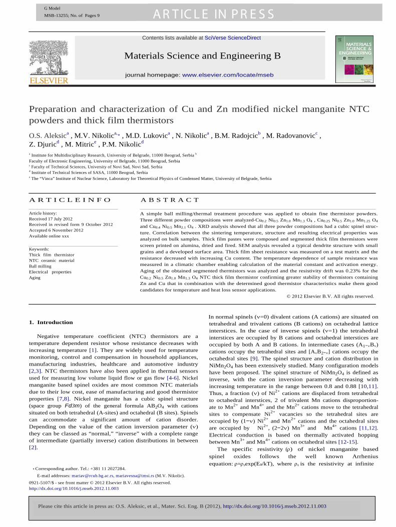
Contents lists available at SciVerse ScienceDirect
Materials Science and Engineering B journal homepage: www.elsevier.com/locate/mseb
Preparation and characterization of Cu and Zn modified nickel manganite NTC powders and thick film thermistors O.S. Aleksica , M.V. Nikolica,∗ , M.D. Lukovica , N. Nikolica , B.M. Radojcicb , M. Radovanovicc , Z. Djuricd , M. Mitrice , P.M. Nikolicd
a Institute for Multidisciplinary Research, University of Belgrade, 11000 Beograd, Serbia b Faculty of Electronic Engineering, University of Belgrade, 11000 Beograd, Serbia c Faculty of Technical Sciences, University of Novi Sad, Novi Sad, Serbia d Institute of Technical Sciences of SASA, 11000 Beograd, Serbia e The “Vinca” Institute of Nuclear Science, Laboratory for Theoretical Physics of Condensed Matter, University of Belgrade, Serbia
A R T I C L E I N F O Article history: Received 17 July 2012 Received in revised form 9 October 2012 Accepted 6 November 2012 Available online xxx
Keywords: Thick film thermistor NTC ceramic material Ball milling Electrical properties Aging
A B S T R A C T
A simple ball milling/thermal treatment procedure was applied to obtain fine thermistor powders. Three different powder compositions were analyzed-Cu0.2 Ni0.5 Zn1.0 Mn1.3 O4 , Cu0.25 Ni0.5 Zn1.0 Mn1.25 O4
and Cu0.4 Ni0.5 Mn2.1 O4 . XRD analysis showed that all three powder compositions had a cubic spinel struc- ture. Correlation between the sintering temperature, structure and resulting electrical properties was analyzed on bulk samples. Thick film pastes were composed and segmented thick film thermistors were screen printed on alumina, dried and fired. SEM analysis revealed a typical dendrite structure with small grains and a developed surface area. Thick film sheet resistance was measured on a test matrix and the resistance decreased with increasing Cu content. The temperature dependence of sample resistance was measured in a climatic chamber enabling calculation of the material constant and activation energy. Aging of the obtained segmented thermistors was analyzed and the resistivity drift was 0.23% for the Cu0.2 Ni0.5 Zn1.0 Mn1.3 O4 NTC thick film thermistor confirming greater stability of thermistors containing Zn and Cu that in combination with the determined good thermistor characteristics make them good candidates for temperature and heat loss sensor applications.
© 2012 Elsevier B.V. All rights reserved.
1. Introduction
Negative temperature coefficient (NTC) thermistors are a temperature dependent resistor whose resistance decreases with increasing temperature [1]. They are widely used for temperature monitoring, control and compensation in household appliances, manufacturing industries, healthcare and automotive industry [2,3]. NTC thermistors have also been applied in thermal sensors used for measuring low volume liquid flow or gas flow [4-6]. Nickel manganite based spinel oxides are most common NTC materials due to their low cost, ease of manufacturing and good thermistor properties [7,8]. Nickel manganite has a cubic spinel structure (space group Fd3m) of the general formula AB2O4 with cations situated on both tetrahedral (A-sites) and octahedral (B sites). Spinels can accommodate a significant amount of cation disorder. Depending on the value of the cation inversion parameter (ν) they can be classed as “normal,” “inverse” with a complete range of intermediate (partially inverse) cation distributions in between [2].
∗ Corresponding author. Tel.: +381 11 2027284.
E-mail addresses: [email protected], [email protected] (M.V. Nikolic). 0921-5107/$ - see front matter © 2012 Elsevier B.V. All rights reserved. http://dx.doi.org/10.1016/j.mseb.2012.11.003
In normal spinels (ν=0) divalent cations (A cations) are situated on tetrahedral and trivalent cations (B cations) on octahedral lattice interstices. In the case of inverse spinels (ν=1) the tetrahedral interstices are occupied by B cations and octahedral interstices are occupied by both A and B cations. In intermediate cases (A1−νBν) cations occupy the tetrahedral sites and [AνB2−ν] cations occupy the octahedral sites [9]. The spinel structure and cation distribution in NiMn2O4 has been extensively studied. Many configuration models have been proposed. The spinel structure of NiMn2O4 is defined as inverse, with the cation inversion parameter decreasing with increasing temperature in the range between 0.8 and 0.88 [10,11]. Thus, a fraction (ν) of Ni2+ cations are displaced from tetrahedral to octahedral interstices, 2 of trivalent Mn cations disproportion- ate to Mn2+ and Mn4+ and the Mn2+ cations move to the tetrahedral sites to compensate Ni2+ vacancies so the tetrahedral sites are occupied by (1−ν) Ni2+ and Mn2+ cations and the octahedral sites are occupied by Ni2+, (2−2ν) Mn3+ and Mn4+ cations [11,12]. Electrical conduction is based on thermally activated hopping between Mn3+ and Mn4+ cations on octahedral sites [12-15].
The specific resistivity (ρ) of nickel manganite based spinel oxides follows the well known Arrhenius equation: ρ=ρ0exp(Ea/kT), where ρ0 is the resistivity at infinite
Please cite this article in press as: O.S. Aleksic, et al., Mater. Sci. Eng. B (2012), http://dx.doi.org/10.1016/j.mseb.2012.11.003
A R T IC L E IN P R E S S G Model
MSB-13255; No. of Pages 9
O.S. Aleksic et al. / Materials Science and Engineering B xxx (2012) xxx-xxx 2
temperature, determined by the total number of octahedral lattice sites that can take place in the hopping process, T is the temperature, Ea is the activation energy for conduction and k is the Boltzmann constant [16,17]. The material constant B (B-value) is defined as Ea/k (with unit temperature in Kelvin) and represents the measure of sensitivity of the thermistor device over a given temperature range. Three parameters are most often used to characterize NTC thermistors: ρ25 - the specific resistivity at room temperature (usually 25◦C), B - the material constant and the aging value that describes the stability of NTC thermistors over time [17].
The electrical properties of nickel manganite based spinel oxides depend strongly on the composition of metal oxides and the microstructure of ceramic materials that effect the cation distribution in the spinel structure [18]. Besides Ni and Mn present in the cubic nickel manganite spinel oxide, different elements such as Cu, Zn, Fe, Co, Mg, Si have been added in varied amounts and combinations while retaining the cubic spinel structure [1,3,8,14,15]. Addition of other metal elements influences the three basic thermistor parameters - ρ25, B-value and stability in different ways [17-25]. These parameters are also strongly influenced by the manufacturing conditions that include the powder preparation procedure and processing conditions such as the sintering temperature, rate of cooling and sintering duration. Different methods have been applied to prepare starting NTC powder such as solid state methods [1,15,21,22,26], sol-gel method [19], solution combustion method [27] and co-precipitation method [8,14,20]. Solid state methods have included solid state coordination reactions of mixed oxalates [1,15,21] or ball milling/thermal treatment of mixed oxides [22,26,28,29].
Mechanical activation (mechanochemical processing) using a high-energy milling process has been widely applied in powder processing, due to its ability to produce materials with improved physical properties [30-33]. The mechanical energy generated by high-energy ball milling serves to activate chemical reactions in the material. Mechanical energy is supposed to thermally activate the atoms in a material in such a way that new positions are taken in accordance with the allowed thermodynamical feasibility [33]. Solid-state reactions involve formation of product phase(s) at the interfaces of the reactants [34]. Intensive milling increases the con- tact between the reactant powder particles due to reduction in particle size and enables fresh surfaces to come into contact and react, thus reducing the reaction temperature. High defect densities induced by intensive milling in high-energy mills accelerate the diffusion process. Particle refinement and consequent reduction in diffusion distances (due to microstructural refinement) also contribute to lowering reaction temperatures [30]. Mechanical activation has been used to synthesize different types of oxides [32-34] and also to modify and improve the properties of synthesized materials [35,36].
Thermistors have been applied in the bulk form or as thick and thin films [3,16]. Taking into account the current trends in electronics toward reducing component dimensions thick film thermistors continue to be in focus. In our previous work we applied thick film segmented thermistors in a simple thermal sensor system for water [4]. One of the disadvantages of this sensor system was the thermistor resistivity that required a relatively high input voltage of 50-125 V to attain a self-heating current of 20 mA. The aim of this work was to (a) synthesize new thermistor powders with a reduced particle size and lower resistivity by introducing Cu and Zn and using a simple ball milling/thermal treatment procedure of starting oxide powders, (b) perform a detailed analysis of the physical properties of bulk samples, including correlation between microstructure and sintering temperature and (c) study the physical properties of thick film segmented thermistors obtained by screen printing using new
thermistor pastes with the aim of applying them in water flow sensors.
2. Experimental Three different oxide powder mixtures were prepared using
initial MnCO3, NiO, ZnO and CuO powders (Aldrich, purity 99.9%) in the appropriate ratio to obtain the following com- positions: Cu0.2 Ni0.5Zn1.0Mn1.3O4, Cu0.25 Ni0.5Zn1.0Mn1.25O4 and Cu0.4Ni0.5Mn2.1O4. The oxide mixtures were milled in a fast planetary ball mill for 2 h (120 min) (Fritsch Pulverisette 5) in stainless steel bowls with stainless steel balls (15 mm in diameter) in the powder to ball ratio 1:20. The obtained powder mixtures were then slowly (6 h) heated in air to 1100◦C, held at this temperature for 4h and finally slowly cooled to room temperature. The calcined powders were then milled again for 30 min under the same milling conditions. The crystal structure and microstructure of the obtained fine powders was analyzed by XRD (Philips PW1050 diffractometer) and SEM (TESCAN Electron Microscope VEGA TS 5130MM) analyses.
Disc shaped samples were formed by pressing the three obtained starting powder mixtures with 0.4 GPa. They were sintered in air in at 800, 900, 1000, 1100 and 1150◦C for 2 h. The structure and morphology of the obtained sintered samples was analyzed by XRD and SEM and EDS (INCA Penta FETX3 energy dispersive system) analyses. Sample density was determined from weight and volume measurements (with a picnometer). Samples were prepared for resistivity measurements by making electrodes using DuPont 4929 N Ag epoxy low resistance paste. Sample resistivity was measured on a HP 34970A multimeter. The temperature dependence of sample resistivity was measured in a climatic chamber in the temperature range from −20 to 130◦C. All measurements were performed on at least three samples and the average resistivity values were determined. Hall measurements were performed on a Hall effect measurement system (Ecopia, HMS 3000) at room temperature for an applied magnetic field of 0.37 T.
Thermistor paste was composed of the fine powder obtained mixed with butyl cellulose as an organic vehicle, small addition of terpineol thinner and 5 wt% lead boron silicon oxide glass frit (glass composition 61% SiO2, 36% B2O3 and 3% PbO). The paste was screen printed on alumina substrata and fired at 850◦C/10 min in a hybrid conveyor furnace in air. The sintered thick film layers had a thickness of about 22.5 m. Electrical characterization of the new NTC thick film pastes was first done on a resistor R-test matrix. Thick film electrodes were printed of conductive past e-PdAg Du Pont 9804 using a wire screen mesh (SD325 mesh/in.), while the thermistor pastes were printed using a wire screen SD200 mesh/in. The R-test matrix was designed to have different sized rectangular resistors. Thick film electrical resistance was measured at low voltage (20 V) by the UI method. Sheet resistance was determined from measurements performed on 2 mm × 2 mm square resistors.
Segmented thermistors with reduced dimensions were printed in the same way as the test matrices on alumina substrata. The actual thermistor size was 25.4 mm × 6.35 mm × 0.6 mm that is two times smaller than the previously used segmented thermistor (50.8 mm × 6.35 mm × 0.5 mm) [4]. This reduced size enables easier application. The temperature dependence of thick film thermistor resistance was measured in a climatic chamber in the temperature range from −20 to 130◦C. All measurements were performed on several samples and the average resistivity values were determined. One of the first obvious advantages of these thermistors was the reduced required input voltage - only 20 V compared to the 80 V in the previously applied thermistors [4]. SEM analysis of the obtained thick film thermistors was performed
Please cite this article in press as: O.S. Aleksic, et al., Mater. Sci. Eng. B (2012), http://dx.doi.org/10.1016/j.mseb.2012.11.003
A R T IC L E IN P R E S S G Model
MSB-13255; No. of Pages 9

G Model MSB-13255; No. of Pages 9
O.S. Aleksic et al. / Materials Science and Engineering B xxx (2012) xxx-xxx 3
on a TESCAN Electron Microscope VEGA TS 5130 MM. Aging of the obtained segmented thermistors using all three
starting thermistor pastes was analyzed by keeping them in a furnace at 150◦C for 800 h. Aging is defined by R/R0 = (R − R0)/R0, where R0 is the resistance at 25◦C (room temperature) before the aging test and R is the resistance at 25◦C after the aging test [1].
3. Results and discussion 3.1. Powder and sintered sample structure
After calcination XRD diagrams of the obtained coarse powders showed a cubic spinel structure for Cu0.4Ni0.5Mn2.1O4 powder. Le- Bail full pattern profile fitting was used to estimate the unit cell parameter as a = 8.38012(19). A tetragonal distorted spinel structure was obtained for Cu0.2 Ni0.5Zn1.0Mn1.3O4 powder (Fig. 1). This is the reason why we also made a powder mixture with just slightly more Cu (x = 0.25). However, even slightly more added Cu did not result in a cubic spinel structure, and a tetragonal distorted spinel structure was also obtained as shown in Fig. 1.
Differences in the spinel structure of Cu and Zn modified nickel manganite spinels is due to the cation distribution that depends on the spinel composition and the applied synthesis process. In manganites deformation of the spinel structure from cubic to tetragonal is due to the cooperative Jahn-Teller effect associated with Mn3+ cations on octahedral (B) sites [37,38]. The Mn3+ content can be modified by reduction of Mn4+ leading to an increase in Mn3+ or oxidation of Mn3+ into Mn4+. The amount of Ni also influences the spinel structure. Substitution of Ni and Mn with Cu and Zn changes
Fig. 1. XRD patterns of Cu0.2 Zn1.0 Ni0.5 Mn1.3 O4 , Cu0.25 Zn1.0 Ni0.5 Mn1.25 O4 and Cu0.4 Ni0.5 Mn2.1 O4 powders calcined at 1100◦ C in air.
the Mn3+ content. Jadhav and Puri [20] analyzed the influence of Cu substitution on structural, electrical and dielectric properties of nickel manganite. Substitution of Ni with Cu linearly increased grain size and sintered density, and decreased porosity. The resistivity also decreased with increased Cu content. This is connected with the cation distribution of Cu in the spinel structure. Extensive research has been performed on Cu containing spinels and most authors agree that Cu is present as Cu2+ and Cu+ [39-41]. Monovalent Cu (Cu+) prefers occupation of tetrahedral sites, while bivalent Cu is present on both octahedral and tetrahedral sites. Zhao et al. [1] analyzed site occupancy in CuxNi0.5Mn2.5−xO4 spinel by XPS analysis and determined that for x=4, the cation distribution is (Mn0.68
2+Cu0.20+Cu0.12
2+)A[Cu0.082+Ni0.5
2+Mn0.784+Mn0.64
3+]BO42−.
X-ray and neutron diffraction investigations of Zn as a substitution for Mn in Mn2.35−xNi0.65ZnxO4 spinel [42] showed that all Ni2+ ions remained located on octahedral sites , while Zn2+ substituted Mn2+ on tetrahedral sites. Possible migration of some Zn2+ was noted during heat treatment for Zn content above 0.75.
In this case our aim was to obtain a powder with a small particle size and a cubic spinel structure. As the structure of the powders with Cu and Zn was a tetragonally distorted spinel structure, we decided to perform additional milling for 30 min.
The performed additional milling of the calcinated powders resulted in a cubic spinel structure for all three powders (Fig. 2). Certain broadening of the peaks after additional milling can be noted, that is probably the consequence of crystallite size reduction and lattice strain promoted by the milling process. Le-Bail full pattern profile fitting was used to
Fig. 2. XRD patterns of Cu0.2 Zn1.0 Ni0.5 Mn1.3 O4 , Cu0.25 Zn1.0 Ni0.5 Mn1.25 O4 and Cu0.4 Ni0.5 Mn2.1 O4 powders additionally milled for 30 min.
Please cite this article in press as: O.S. Aleksic, et al., Mater. Sci. Eng. B (2012), http://dx.doi.org/10.1016/j.mseb.2012.11.003
A R T IC L E IN P R E S S
G Model
MSB-13255; No. of Pages 9
4
O.S. Aleksic et al. / Materials Science and Engineering B xxx (2012) xxx-xxx
Fig. 3. SEM micrographs of starting Cu0.2 Ni0.5 Zn1.0 Mn1.3 O4 , Cu0.25 Ni0.5 Zn1.0 Mn1.25 O4 and Cu0.4 Ni0.5 Mn2.1 O4 powders. calculate unit cell parameters as a=8.372(4)A˚ for Cu0.4Ni0.5Mn2.1O4, a=8.369(5) Å for Cu0.2 Ni0.5Zn1.0Mn1.3O4 and a = 8.3804(9) Å for Cu0.25
Ni0.5Zn1.0Mn1.25O4. Thus addition mechanical activation promoted further contacts and reactions between particle surfaces reducing
the structural distortion structure due to the Jahn-Teller effect (due to distorting Mn3+cations on octahedral (B) sites). Obviously further optimization of the milling/calcination parameters (milling time/sintering temperature) is possible and could be the subject of
Fig. 4. XRD patterns of Cu0.4 Ni0.5 Mn2.1 O4 ceramics sintered at 1100◦ C, inset-sintered at 900◦ C.
Please cite this article in press as: O.S. Aleksic, et al., Mater. Sci. Eng. B (2012), http://dx.doi.org/10.1016/j.mseb.2012.11.003
A R T IC L E IN P R E S S
G Model
MSB-13255; No. of Pages 9 O.S. Aleksic et al. / Materials Science and Engineering B xxx (2012) xxx-xxx 5
further investigations.
The SEM microstructure of the starting powders is shown in Fig. 3. The morphology of the obtained powder shows that the powder particle size is uneven and irregular with a distribution of small particles (around 200 nm) and larger agglomerates. Agglomeration of particles can be explained as a common way to minimize their surface free energy.
The determined unit cell parameters were used to calculate the theoretical density and we obtained ρth = 5.3 g/cm3 for Cu0.4Ni0.5Mn2.1O4, ρth = 5.504 g/cm3 for Cu0.2Ni0.5Zn1.0Mn1.3O4 and ρth = 5.492 g/cm3 for Cu0.25Ni0.5Zn1.0Mn1.25O4.
XRD, SEM and EDS analyses of sintered samples showed changes in the sample composition and microstructure with changes in the sintering temperature. XRD analysis showed that, besides a cubic spinel structure C0.4Ni0.5Mn2.1O4 sintered samples contained a CuO second phase (Fig. 4). This phase is present at all sintering temperatures. Lattice parameters determined using Le-Bail full pattern profile fitting for the sample sinteredat 1100◦C calculated a = 8.3093(1) for the cubic spinel phase (space group Fd3m) and a = 4.6901(2), b = 3.4289(2) and c = 5.1340(4) for the CuO phase (space group C2/c).
In the case of Cu0.2 Ni0.5Zn1.0Mn1.3O4 and Cu0.25Ni0.5Zn1.0Mn1.25O4 besides a cubic spinel structure the second phase was a rock salt (NiO) cubic structure, with a small amount of CuO, as shown for a Cu0.2Ni0.5Zn1.0Mn1.3O4 sample sintered at 1100◦C on Fig. 5. Lattice parameters determined using Le-Bail full pattern profile fitting of the Cu0.2Ni0.5Zn1.0Mn1.3O4 sample sintered at 1100◦C calculated a = 8.3325(3) for the cubic
Fig. 5. XRD patterns of Cu0.2 Ni0.5 Zn1.0 Mn1.3 O4 ceramics sintered at 1100◦ C.
spinel phase, a = 8.4305(8) for the NiO rock salt phase (space group Fm3m) and a = 4.687(2), b = 3.401(3) and c = 5.231(4) for the CuO phase. These phases are present in both sample types at all sintering temperatures.
The obtained sintered sample density increased with the sintering temperature (Fig. 6). Sample porosity decreased with increase in sintering temperature, with smaller closed pores replacing the larger more irregular ones obtained at lower sintering temperatures.
Fig. 6. Changes in density and microstructure with increase in the sintering temperature.
Please cite this article in press as: O.S. Aleksic, et al., Mater. Sci. Eng. B (2012), http://dx.doi.org/10.1016/j.mseb.2012.11.003
A R T IC L E IN P R E S S
G Model
MSB-13255; No. of Pages 9
6
O.S. Aleksic et al. / Materials Science and Engineering B xxx (2012) xxx-xxx
Fig. 7. Back scattering (BSE) image and EDS analysis of Cu0.2 Ni0.5 Zn1.0 Mn1.3 O4 (a) and Cu0.4 Ni0.5 Mn2.1 O4 (b) samples sintered at 1100◦ C.
temperatures. According to Zhu et al. [43] at temperatures above 1050◦C in air reduction of Cu2+ to Cu+ leads to emission of O2 leaving extra closed pores in the ceramics. The sintered sample density varied between 88 and 93% for Cu0.4Ni0.5Mn2.1O4 samples and 92-95% for Cu0.2Ni0.5Zn1.0Mn1.3O4 and Cu0.2Ni0.5Zn1.0Mn1.3O4, with a slightly denser structure for the sample with less Cu (x = 0.2). Addition of Zn resulted in slightly smaller pores.
SEM and EDS analysis showed that there was a low contamination of powders from the milling media as shown in Fig. 7. The average amount of Fe present in samples was 0.5 at.%. 3.2 Electrical properties of bulk samples
The electrical resistivity of Cu0.2 Ni0.5Zn1.0Mn1.3O4, Cu0.25 Ni0.5Zn1.0Mn1.25O4 and Cu0.4Ni0.5Mn2.1O4 samples measured at room temperature (25◦C) are given in Fig. 8. One can note that the electrical resistivity decreased with increased sintering temperature. Similar values were obtained for samples with0.2 and 0.25 Cu and they were in the range 3746-2015 Ωcm depending on the sintering temperature, while in the case of Cu0.4Ni0.5Mn2.1O4 samples electrical resistivity was much lower and in the range 49.4-36.7 Ωcm depending on the sintering temperature.
Decrease in electrical resistivity with increase in the sintering temperature can be explained by changes in the sample density, grain size and microstructure with increased sintering temperatures. Changes of sample microstructure with changes in the sample density are shown in Fig. 6, where one can see that with increased sintering temperature the sample density increased, the
pores became smaller and closed porosity was noted for samples sintered at 1000◦C and above.
Differences between the electrical resistivity between samples containing Cu and samples containing Cu and Zn are connected with the nature and amount of the added elements (Cu and Zn) and cation distribution in the spinel structure. Changes in resistivity are also the result of differences in grain size, crystal structure, imperfections and microstructure homogeneity [20].
In nickel manganite electrical conductivity is based on thermally activated hopping between Mn3+ and Mn4+ cations on octahedral (B) sites. The exact nature of valences and distribution of cations in this inverse spinel structure (AB2O4) has been extensively investigated and many models for the valence configuration have been proposed [2]. According to Asbrink et al. [11] the proposed cation
Fig. 8. Electrical resistivity of Cu0.2 Ni0.5 Zn1.0 Mn1.3 O4 (a), Cu0.25 Ni0.5 Zn1.0 Mn1.25 O4 (b), and Cu0.4 Ni0.5 Mn2.1 O4 (c) samples measured at room temperature (25◦C) depending on the sample sintering temperature.
Please cite this article in press as: O.S. Aleksic, et al., Mater. Sci. Eng. B (2012), http://dx.doi.org/10.1016/j.mseb.2012.11.003
A R T IC L E IN P R E S S

O.S. Aleksic et al. / Materials Science and Engineering B xxx (2012) xxx-xxx 7
Fig. 9. Resistance of Cu0.2 Ni0.5 Zn1.0 Mn1.3 O4 (a), Cu0.25 Ni0.5 Zn1.0 Mn1.25 O4 (b), and Cu0.4 Ni0.5 Mn2.1 O4 (c) samples sintered at 1000◦ C measured in a climatic chamber in the temperature range −20 to 120◦ C.
distribution was (Ni1−ν2+Mnν
2+)A[Niν2+Mn2−2ν3+Mnν
4+]BO42−.
The inversion parameter was determined as = 0.87 at 115 K and 0.8 at room temperature. In any case it can be concluded that Ni ions prefer the occupation of octahedral (B) sites, while Mn ions partially occupy both tetrahedral and octahedral sites depending on the value of cation inversion parameter.
A possible explanation of the decrease in resistivity due to the presence of Cu is that occupation of tetrahedral (A) sites with Cu that is replacing Ni commonly occupying octahedral (B) sites leads to migration of Mn ions from A sites to B sites, thus increasing the amount of Mn3+ and Mn4+ ions responsible for conduction with added participation of Cu+ and Cu2+ cations at octahedral (B) sites in the hopping process.
On the other hand, XPS analysis of the cation distribution in spinel structures containing both Cu and Zn showed that prefer- ential occupation of tetrahedral (A) sites with Zn2+ lead to a reduction, if not disappearance of Cu ions on tetrahedral sites [1]. In Zn1.0CuxNi0.5Mn1.5−xO4, XPS spectra showed one peak for x = 0.4, indicating that all Cu ions have converted to Cu2+, while for x = 0.2 a large peak was assigned to Cu2+, while a small peak was assigned to Cu+ [1]. From the viewpoint of changes in electrical resistivity, the presence of Zn on tetrahedral sites reduced significantly the presence of Cu+ on tetrahedral sites, and as Cu+ and Cu2+ ions on tetrahedral sites participate in the hopping process this could account for the lower conductivity and higher resistivity of samples containing both Cu and Zn compared to samples containing only Cu. Investigations of the influence of the Zn content on the structure and electrical properties of ZnxCu0.2Ni0.66Mn2.14−xO4 spinel samples also showed that increase of the Zn content resulted in increased electrical resistivity due to reduction of Cu ions on tetrahedral (A) sites [17].
Measurements of resistance of all three sample types sintered at 1000◦C in a climatic chamber in the temperature range −20 to 120◦
showed an exponential decrease in the resistance with increase in temperature (Fig. 9). The activation energy (Ea) was calculated from the slope of the lnρ − 1/T curve (Fig. 10) and the material constant (B-value) was determined as Ea/k (k is the Boltzmann constant) and
Fig. 10. Relationship between log and 1/T for Cu0.2 Ni0.5 Zn1.0 Mn1.3 O4 , Cu0.25
Ni0.5 Zn1.0 Mn1.25 O4 and Cu0.4 Ni0.5 Mn2.1 O4 samples sintered at 1000◦ C.
these values are given in Table 1. The results determined for the material constant are in accordance with the findings of Zhao et al. [1]. Hall measurements gave values for the carrier mobility ( ) and average Hall coefficient (RH), as shown in Table 1, that also change with changes in the Cu content.
3.3. Structural and electrical properties of thick film samples
SEM analysis of the obtained thick film thermistors showed a
typical dendrite structure with small grains and a developed sur- face area that is characteristic for thick film samples. A slightly more homogenous grain size distribution and less porous struc- ture was obtained for samples containing Zn (Fig. 11a). Although
Table 1. Resistivity at 20◦ C (ρ20), carrier mobility (µ), average Hall coefficient (RH ),B-value (material constant) and activation energy of bulk Cu0.2 Ni0.5Zn1.0Mn1.3O4, Cu0.25
Ni0.5 Zn1.0 Mn1.25 O4 and Cu0.4 Ni0.5 Mn2.1 O4 NTC thermistor samples sintered at 1000◦ C.
Sample ρ20 (Ω cm) µ(cm2 /Vs) RH (cm3 /C) B (K) Ea (eV)
Cu0.2 Ni0.5 Zn1.0 Mn1.3 O4 2555 1499 1.617 × 10⁶ 3424 0.299 Cu0.25 Ni0.5 Zn1.0 Mn1.25 O4 2222 437 1.593 × 10⁶ 3406 0.298
Cu0.4 Ni0.5 Mn2.1 O4 45.97 147 5.610 × 10² 2632 0.231
G Model MSB-13255; No. of Pages 9
Please cite this article in press as: O.S. Aleksic, et al., Mater. Sci. Eng. B (2012), http://dx.doi.org/10.1016/j.mseb.2012.11.003
A R T IC L E IN P R E S S

ARTICLE IN PRESS 8 O.S. Aleksic et al. / Materials Science and Engineering B xxx (2012) xxx-xxx
Fig. 11. SEM micrograph of Cu0.25Ni0.5Zn1.0Mn1.25O4 and Cu0.4Ni0.5 Mn2.1O4 thick film samples: (a and b) sample surfaces, respectively and (c and d) sample cross sections, respectively
agglomeration was significantly lowered by mixing the starting powder with a viscous organic vehicle for 24 h grains were joined in clusters. SEM images of thick film cross-sections are also shown in Fig. 11.
Measurements of sheet resistance of all three thick film sample types showed that similar values were obtained for samples containing Zn, and a three times lower value for the Cu0.4Ni0.5Mn2.1O4 sample (Table 2).
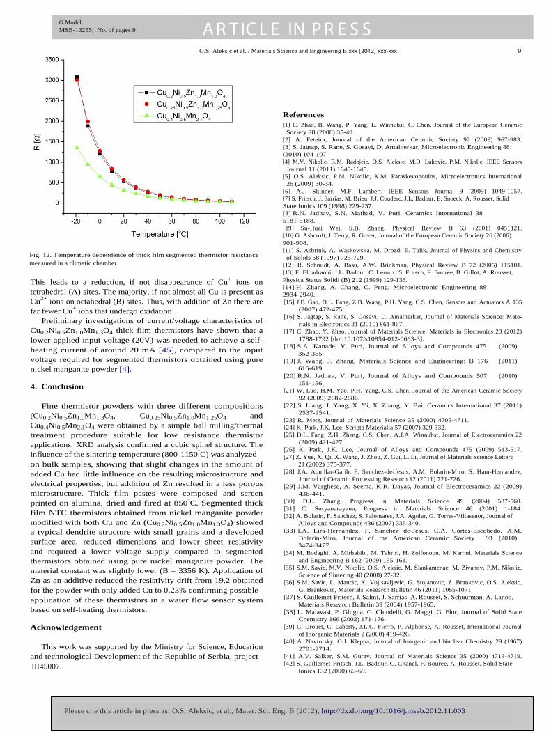
Measurements of thick film thermistor resistance showed an exponential decrease in resistance with increase in temperature similar to the bulk samples (Fig. 12). It is interesting to observe that the difference in resistance values between samples containing Zn and Cu and only Cu is less than in the case of bulk samples. This can be explained by the lower sintering temperature
Table 2 Sheet resistance at 25◦ C (given in Mohm/square), B-value (material constant) and activation energy of thick film Cu0.2 Ni0.5 Zn1.0 Mn1.3 O4 , Cu0.25 Ni0.5 Zn1.0 Mn1.25 O4 and Cu0.4 Ni0.5 Mn2.1 O4 NTC thermistor (measured on a 2.5 mm × 2.5 mm test resistor).
Sample Rsq (M Ω /sq) B(K) Ea (eV)
Cu0.2 Ni0.5 Zn1.0 Mn1.3 O4 1.3 3356 0.294 Cu0.25 Ni0.5 Zn1.0 Mn1.25 O4 1.2 3294 0.288 Cu0.4 Ni0.5 Mn2.1 O4 0.39 2915 0.255
of thick films (850◦C) and also the slightly more homogenous grain size distribution and less porous structure obtained for samples containing Zn. The activation energy was calculated from the slope of the ln − 1/T curve and the B-value (material constant) was calculated in the same way as for bulk samples and they are given in Table 2. One can note that similar activation energy and B-values were obtained as in the case of bulk samples. The B-values were around 3300 for samples containing Zn and around 2900 for the Cu0.4Ni0.5Mn2.1O4 sample suitable for application in thermal measurement systems such as water flow sensors.
The resistivity drift was calculated for Cu0.2Ni0.5Zn1.0Mn1.3O4, Cu0.25Ni0.5Zn1.0Mn1.25O4 and Cu0.4Ni0.5Mn2.1O4 thick film thermistor samples after annealing at 150◦C in air for 800 h. The thermistors containing Zn were very stable, with the drift of 0.23 and 0.51% for Cu0.2Ni0.5Zn1.0Mn1.3O4, Cu0.25Ni0.5Zn1.0Mn1.25O4 thick film thermistor samples, respectively. The drift was much larger for the Cu0.4Ni0.5Mn2.1O4 thick film thermistor - 19.2% con- firming previous reports of oxidation of Cu+ ions at A-sites to Cu2+
ions by atmospheric oxygen at temperatures below 300◦C followed by migration of Cu ions from A to B sites in the cubic spinel structure [44]. This confirms the results of Zhao et al. [1] obtained on bulk samples of the same composition. In the cubic spinel structure containing Zn, Zn2+ ions almost exclusively occupy A sites.
Please cite this article in press as: O.S. Aleksic, et al., Mater. Sci. Eng. B (2012), http://dx.doi.org/10.1016/j.mseb.2012.11.003
G Model MSB-13255; No. of pages 9
O.S. Aleksic et al. / Materials Science and Engineering B xxx (2012) xxx-xxx 9
Fig. 12. Temperature dependence of thick film segmented thermistor resistance measured in a climatic chamber This leads to a reduction, if not disappearance of Cu+ ions on tetrahedral (A) sites. The majority, if not almost all Cu is present as Cu2+ ions on octahedral (B) sites. Thus, with addition of Zn there are far fewer Cu+ ions that undergo oxidation.
Preliminary investigations of current/voltage characteristics of Cu0.2Ni0.5Zn1.0Mn1.3O4 thick film thermistors have shown that a lower applied input voltage (20V) was needed to achieve a self-heating current of around 20 mA [45], compared to the input voltage required for segmented thermistors obtained using pure nickel manganite powder [4]. 4. Conclusion
Fine thermistor powders with three different compositions (Cu0.2Ni0.5Zn1.0Mn1.3O4, Cu0.25Ni0.5Zn1.0Mn1.25O4 and Cu0.4Ni0.5Mn2.1O4 were obtained by a simple ball milling/thermal treatment procedure suitable for low resistance thermistor applications. XRD analysis confirmed a cubic spinel structure. The influence of the sintering temperature (800-1150◦C) was analyzed on bulk samples, showing that slight changes in the amount of added Cu had little influence on the resulting microstructure and electrical properties, but addition of Zn resulted in a less porous microstructure. Thick film pastes were composed and screen printed on alumina, dried and fired at 850◦C. Segmented thick film NTC thermistors obtained from nickel manganite powder modified with both Cu and Zn (Cu0.2Ni0.5Zn1.0Mn1.3O4) showed a typical dendrite structure with small grains and a developed surface area, reduced dimensions and lower sheet resistivity and required a lower voltage supply compared to segmented thermistors obtained using pure nickel manganite powder. The material constant was slightly lower (B = 3356 K). Application of Zn as an additive reduced the resistivity drift from 19.2 obtained for the powder with only added Cu to 0.23% confirming possible application of these thermistors in a water flow sensor system based on self-heating thermistors. Acknowledgement
This work was supported by the Ministry for Science, Education
and technological Development of the Republic of Serbia, project III45007.
References [1] C. Zhao, B. Wang, P. Yang, L. Winnubst, C. Chen, Journal of the European Ceramic Society 28 (2008) 35-40. [2] A. Feteira, Journal of the American Ceramic Society 92 (2009) 967-983. [3] S. Jagtap, S. Rane, S. Gosavi, D. Amalnerkar, Microelectronic Engineering 88 (2010) 104-107. [4] M.V. Nikolic, B.M. Radojcic, O.S. Aleksic, M.D. Lukovic, P.M. Nikolic, IEEE Sensors Journal 11 (2011) 1640-1645. [5] O.S. Aleksic, P.M. Nikolic, K.M. Paraskevopoulos, Microelectronics International 26 (2009) 30-34. [6] A.J. Skinner, M.F. Lambert, IEEE Sensors Journal 9 (2009) 1049-1057. [7] S. Fritsch, J. Sarrias, M. Brieu, J.J. Couderc, J.L. Badour, E. Snoeck, A. Rousset, Solid State Ionics 109 (1998) 229-237. [8] R.N. Jadhav, S.N. Mathad, V. Puri, Ceramics International 38 5181-5188.
[9] Su-Huai Wei, S.B. Zhang, Physical Review B 63 (2001) 0451121. [10] G. Ashcroft, I. Terry, R. Gover, Journal of the European Ceramic Society 26 (2006) 901-908. [11] S. Asbrink, A. Waskowska, M. Drozd, E. Talik, Journal of Physics and Chemistry of Solids 58 (1997) 725-729. [12] R. Schmidt, A. Basu, A.W. Brinkman, Physical Review B 72 (2005) 115101. [13] E. Elbadraoui, J.L. Badour, C. Leroux, S. Fritsch, F. Bouree, B. Gillot, A. Rousset, Physica Status Solidi (B) 212 (1999) 129-133. [14] H. Zhang, A. Chang, C. Peng, Microelectronic Engineering 88 2934-2940. [15] J.F. Gao, D.L. Fang, Z.B. Wang, P.H. Yang, C.S. Chen, Sensors and Actuators A 135 (2007) 472-475. [16] S. Jagtap, S. Rane, S. Gosavi, D. Amalnerkar, Journal of Materials Science: Mate- rials in Electronics 21 (2010) 861-867. [17] C. Zhao, Y. Zhao, Journal of Materials Science: Materials in Electronics 23 (2012) 1788-1792 [doi:10.107/s10854-012-0663-3]. [18] S.A. Kanade, V. Puri, Journal of Alloys and Compounds 475 (2009)
352-355. [19] J. Wang, J. Zhang, Materials Science and Engineering: B 176 (2011)
616-619. [20] R.N. Jadhav, V. Puri, Journal of Alloys and Compounds 507 (2010)
151-156. [21] W. Luo, H.M. Yao, P.H. Yang, C.S. Chen, Journal of the American Ceramic Society 92 (2009) 2682-2686. [22] S. Liang, J. Yang, X. Yi, X. Zhang, Y. Bai, Ceramics International 37 (2011) 2537-2541. [23] R. Metz, Journal of Materials Science 35 (2000) 4705-4711. [24] K. Park, J.K. Lee, Scripta Materialia 57 (2007) 329-332. [25] D.L. Fang, Z.H. Zheng, C.S. Chen, A.J.A. Winnubst, Journal of Electroceramics 22 (2009) 421-427. [26] K. Park, J.K. Lee, Journal of Alloys and Compounds 475 (2009) 513-517. [27] Z. Yue, X. Qi, X. Wang, J. Zhou, Z. Gui, L. Li, Journal of Materials Science Letters
21 (2002) 375-377. [28] J.A. Aquillar-Garib, F. Sanchez-de-Jesus, A.M. Bolarin-Miro, S. Ham-Hernandez, Journal of Ceramic Processing Research 12 (2011) 721-726. [29] J.M. Varghese, A. Seema, K.R. Dayas, Journal of Electroceramics 22 (2009) 436-441. [30] D.L. Zhang, Progress in Materials Science 49 (2004) 537-560. [31] C. Suryanarayana, Progress in Materials Science 46 (2001) 1-184. [32] A. Bolarin, F. Sanchez, S. Palomares, J.A. Agular, G. Torres-Villasenor, Journal of
Alloys and Compounds 436 (2007) 335-340. [33] I.A. Lira-Hernandez, F. Sanchez de-Jesus, C.A. Cortes-Escobedo, A.M. Bolarin-Miro, Journal of the American Ceramic Society 93 (2010)
3474-3477. [34] M. Bodaghi, A. Mirhabibi, M. Tahriri, H. Zolfonoon, M. Karimi, Materials Science and Engineering B 162 (2009) 155-161. [35] S.M. Savic, M.V. Nikolic, O.S. Aleksic, M. Slankamenac, M. Zivanov, P.M. Nikolic, Science of Sintering 40 (2008) 27-32. [36] S.M. Savic, L. Mancic, K. Vojisavljevic, G. Stojanovic, Z. Brankovic, O.S. Aleksic, G. Brankovic, Materials Research Bulletin 46 (2011) 1065-1071. [37] S. Guillemet-Fritsch, J. Salmi, J. Sarrias, A. Rousset, S. Schuurman, A. Lanoo,
Materials Research Bulletin 39 (2004) 1957-1965. [38] L. Malavasi, P. Ghigna, G. Chiodelli, G. Maggi, G. Flor, Journal of Solid State Chemistry 166 (2002) 171-176. [39] C. Drouet, C. Laberty, J.L.G. Fierro, P. Alphonse, A. Rousset, International Journal of Inorganic Materials 2 (2000) 419-426. [40] A. Navrotsky, O.J. Kleppa, Journal of Inorganic and Nuclear Chemistry 29 (1967) 2701-2714. [41] A.V. Salker, S.M. Gurav, Journal of Materials Science 35 (2000) 4713-4719. [42] S. Guillemet-Fritsch, J.L. Badour, C. Chanel, F. Bouree, A. Rousset, Solid State
Ionics 132 (2000) 63-69.
A R T IC L E IN P R E S S G Model MSB-13255; No. of pages 9
Please cite this article in press as: O.S. Aleksic, et al., Mater. Sci. Eng. B (2012), http://dx.doi.org/10.1016/j.mseb.2012.11.003

[43] Y. Zhu, K. Mimura, M. Isshiki, Oxidation of Metals 62 (2004) 207-222. [44] B. Gillot, S. Buguet, E. Kester, C. Baubet, Ph. Tailhades, Thin Solid Films 357
(1999) 223-231. [45] M.V. Nikolic, O.S. Aleksic, B. Radojcic, M.D. Lukovic, N. Nikolic, Z. Djuric, Optimization and application of NTC thick film segmented thermistors,
in: Proceedings of the International Conference on Materials and Applica- tions for Sensors and Transducers, IC-MAST, May 24-28, Budapest, Hungary, 2012.
G Model MSB-13255; No. of pages 9
Please cite this article in press as: O.S. Aleksic, et al., Mater. Sci. Eng. B (2012), http://dx.doi.org/10.1016/j.mseb.2012.11.003
A R T IC L E IN P R E S S