˘ ˇ ˆ µ - futurlec.com instruments semiconductor products and disclaimers thereto appears at the...
TRANSCRIPT
µ
SLOS193B − FEBRUARY 1997 − REVISED MAY 2004
1POST OFFICE BOX 655303 • DALLAS, TEXAS 75265
2× Bandwidth (2 MHz) of the TL06x andTL03x Operational Amplifiers
Low Supply Current . . . 290 µA/Ch Typ
On-chip Offset Voltage Trimming forImproved DC Performance
High Output Drive, Specified into 100- ΩLoads
Lower Noise Floor Than EarlierGenerations of Low-Power BiFETs
description
The TLE206x series of low-power JFET-input operational amplifiers doubles the bandwidth of the earliergeneration TL06x and TL03x BiFET families without significantly increasing power consumption. TexasInstruments Excalibur process also delivers a lower noise floor than the TL06x and TL03x. On-chip zenertrimming of offset voltage yields precision grades for dc-coupled applications. The TL206x devices arepin-compatible with other Texas Instruments BiFETs; they can be used to double the bandwidth of TL06x andTL03x circuits or to reduce power consumption of TL05x, TL07x, and TL08x circuits by nearly 90%.
BiFET operational amplifiers offer the inherently-higher input impedance of the JFET-input transistors, withoutsacrificing the output drive associated with bipolar amplifiers. This makes them better suited for interfacing withhigh-impedance sensors or low-level ac signals. They also feature inherently better ac response than bipolaror CMOS devices having comparable power consumption. The TLE206x family features a high-output-drivecircuit capable of driving 100-Ω loads at supplies as low as ±5 V. This makes them uniquely suited for drivingtransformer loads in modems and other applications requiring good ac characteristics, low power, and highoutput drive.
Because BiFET operational amplifiers are designed for use with dual power supplies, care must be taken toobserve common-mode input voltage limits and output swing when operating from a single supply. DC biasingof the input signal is required and loads should be terminated to a virtual ground node at mid-supply. TexasInstruments TLE2426 integrated virtual ground generator is useful when operating BiFET amplifiers from singlesupplies.
The TLE206x are fully specified at ±15 V and ±5 V. For operation in low-voltage and/or single-supply systems,Texas Instruments LinCMOS families of operational amplifiers (TLC- and TLV-prefixes) are recommended.When moving from BiFET to CMOS amplifiers, particular attention should be paid to slew rate and bandwidthrequirements and output loading. The Texas Instruments TLV2432 and TLV2442 CMOS operational amplifiersare excellent choices to consider.
Copyright 2004, Texas Instruments Incorporated !"#$%&" ' ()##*& %' "! +),-(%&" .%&*/#".)(&' ("!"#$ &" '+*(!(%&"' +*# &0* &*#$' "! *%' '&#)$*&''&%.%#. 1%##%&2/ #".)(&" +#"(*''3 ."*' "& *(*''%#-2 (-).*&*'&3 "! %-- +%#%$*&*#'/
Please be aware that an important notice concerning availability, standard warranty, and use in critical applications ofTexas Instruments semiconductor products and disclaimers thereto appears at the end of this data sheet.

µ
SLOS193B − FEBRUARY 1997 − REVISED MAY 2004
2 POST OFFICE BOX 655303 • DALLAS, TEXAS 75265
TLE2061 AVAILABLE OPTIONS
PACKAGED DEVICES
TAVIOmaxAT 25°C
SMALLOUTLINE†
(D)
CHIPCARRIER
(FK)
CERAMICDIP(JG)
PLASTICDIP(P)
TSSOP‡
(PW)
CERAMICFLAT PACK
(U)
500 µV — — — — — —
0°C to 70°C 1.5 mV TLE2061ACD — — TLE2061ACP — —0 C to 70 C
3 mV TLE2061CD — — TLE2061CP TLE2061CPWLE —
500 µV — — — — — —
−40°C to 85°C 1.5 mV TLE2061AID — — TLE2061AIP — —−40 C to 85 C
3 mV TLE2061ID — — TLE2061IP — —
500 µV — — TLE2061BMJG — — —
−55°C to 125°C 1.5 mV TLE2061AMD TLE2061AMFK TLE2061AMJG — — TLE2061AMU−55 C to 125 C
3 mV TLE2061MD TLE2061MFK TLE2061MJG — — TLE2061MU
† The D packages are available taped and reeled. Add R suffix to device type (e.g., TLE2061ACDR).Chips are tested at 25°C.‡ The PW package is available left-end taped and reeled (indicated by the LE suffix on the device type (e.g., TLE2061CPWLE).
TLE2062 AVAILABLE OPTIONS
PACKAGED DEVICES
TAVIOmaxAT 25°C
SMALL OUTLINE †
(D)CHIP CARRIER
(FK)CERAMIC DIP
(JG)PLASTIC DIP
(P)
CERAMICFLAT PACK
(U)
0°C to
70°C
1 mV2 mV4 mV
TLE2062BCDTLE2062ACDTLE2062CD
———
———
TLE2062BCPTLE2062ACPTLE2062CP
———
−40°C to
85°C
1 mV2 mV4 mV
TLE2062BIDTLE2062AIDTLE2062ID
———
———
TLE2062BIPTLE2062AIPTLE2062IP
———
−55°C to
125°C
1 mV2 mV4 mV
TLE2062BMDTLE2062AMDTLE2062MD
—TLE2062AMFKTLE2062MFK
TLE2062BMJGTLE2062AMJGTLE2062MJG
———
—TLE2062AMUTLE2062MU
† The D packages are available taped and reeled. Add R suffix to device type (e.g., TLE2062ACDR).
TLE2064 AVAILABLE OPTIONS
PACKAGED DEVICES
VIOmax SMALL OUTLINE † CHIP CARRIER CERAMIC DIP PLASTIC DIPCERAMIC
TAVIOmaxAT 25°C
SMALL OUTLINE †
(D)CHIP CARRIER
(FK)CERAMIC DIP
(J)PLASTIC DIP
(N)
CERAMICFLAT PACKTA AT 25°C (D) (FK) (J) (N)FLAT PACK
(W)
0°Cto
70°C
2 mV4 mV6 mV
—TLE2064ACDTLE2064CD
— —TLE2064BCNTLE2064ACNTLE2064CN
—
−40°Cto
85°C
2 mV4 mV6 mV
—TLE2064AIDTLE2064ID
— —TLE2064BINTLE2064AINTLE2064IN
—
−55°Cto
125°C
2 mV4 mV6 mV
—TLE2064AMDTLE2064MD
TLE2064BMFKTLE2064AMFKTLE2064MFK
TLE2064BMJTLE2064AMJTLE2064MJ
——
TLE2064AMWTLE2064MW
† The D packages are available taped and reeled. Add R suffix to device type, (e.g., TLE2064ACDR).

µ
SLOS193B − FEBRUARY 1997 − REVISED MAY 2004
3POST OFFICE BOX 655303 • DALLAS, TEXAS 75265
1
2
3
4
8
7
6
5
OFFSET N1IN−IN+
VCC −
NCVCC+OUTOFFSET N2
NC − No internal connection
3 2 1 20 19
9 10 11 12 13
4
5
6
7
8
18
17
16
15
14
NCVCC+NCOUTNC
NCIN −NC
IN +NC
NC
OF
FS
ET
N1
NC
NC
NC
NC
NC
OF
FS
ET
N2
NC
CC
−V
TLE2061, TLE2061A, AND TLE2061BD, DB, JG, P, OR PW PACKAGE
(TOP VIEW)
TLE2061M, TLE2061AM, TLE2061BMFK PACKAGE(TOP VIEW)
1
2
3
4
8
7
6
5
1OUT1IN−1IN+
VCC−
VCC+2OUT2IN−2IN+
3 2 1 20 19
9 10 11 12 13
4
5
6
7
8
18
17
16
15
14
NC2OUTNC2IN−NC
NC1IN−
NC1IN+
NC
NC
NC
NC
NC
NC
VN
C2I
N+
CC
−
VC
C +
1OU
T
TLE2062, TLE2062A, TLE2062BD, JG, OR P PACKAGE
(TOP VIEW)
TLE2062M, TLE2062AM, TLE2062BMFK PACKAGE(TOP VIEW)
4OU
T
3 2 1 20 19
9 10 11 12 13
4
5
6
7
8
18
17
16
15
14
4IN+NCVCC−NC3IN+
1IN+NC
VCC+NC
2IN+
1IN
−1O
UT
NC
3IN
−4I
N −
2IN
−
NC
3OU
T
1
2
3
4
5
6
7
14
13
12
11
10
9
8
1OUT1IN−1IN+
VCC +2IN+2IN−
2OUT
4OUT4IN−4IN+VCC−3IN+3IN−3OUT
2OU
T
TLE2064, TLE2064A, TLE2064BD, J, N, OR W PACKAGE
(TOP VIEW)
TLE2064M, TLE2064AM, TLE2064BMFK PACKAGE(TOP VIEW)
TLE2061 AND TLE2061AU PACKAGE(TOP VIEW)
TLE2062 AND TLE2062AU PACKAGE(TOP VIEW)
1
2
3
4
5
10
9
8
7
6
NCOFFSET N1
IN−IN+
VCC−
NCNCVCC+OUTOFFSET N2
1
2
3
4
5
10
9
8
7
6
NC1OUT
1IN−1IN+
VCC−
NCVCC+2OUT2IN−2IN+
44 44µSLOS193B − FEBRUARY 1997 − REVISED APRIL 2004
Template Release Date: 7−11−94
44
4 POST OFFICE BOX 655303 DALLAS, TEXAS 75265•
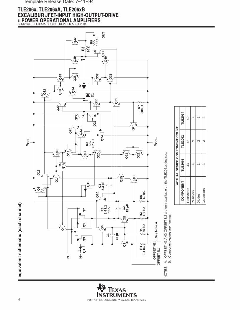
equi
vale
nt s
chem
atic
(ea
ch c
hann
el)
Q20
VC
C−
VC
C+
Q13
Q9
Q14
Q16
Q4
IN+
IN−
Q1
Q5
Q7
Q3
Q6
C1
Q2
Q12
Q15
Q21
Q22
Q26
Q31
Q10
Q11
Q18
Q19
Q25
Q27
Q17
Q23
Q28
Q24
D1
Q30
Q29
Q32
Q35
Q33 Q
34Q
36
D2
Q37
Q38
Q40
Q41
Q42
Q39
OU
T
R1
1.1
kΩR
455
kΩ
R2
1.1
kΩ
Q8
15 p
F
R6
2.7
kΩ
R8
20 Ω
R9
100
Ω
R7
600
ΩR
560
kΩ
R3
2.4
kΩ
C3
5.3
pF
C2
15 p
F
See
Not
e A
OF
FS
ET
N2
OF
FS
ET
N1
NO
TE
S:
A.
OF
FS
ET
N1
AN
D O
FF
SE
T N
2 ar
e on
ly a
vaili
able
on
the
TLE
2061
x de
vice
s.B
.C
ompo
nent
val
ues
are
nom
inal
.
AC
TU
AL
DE
VIC
E C
OM
PO
NE
NT
CO
UN
T
CO
MP
ON
EN
TT
LE20
61T
LE20
62T
LE20
64
Tran
sist
ors
4342
42
Res
isto
rs9
99
Dio
des
12
2
Cap
acito
rs3
33

µ
SLOS193B − FEBRUARY 1997 − REVISED MAY 2004
5POST OFFICE BOX 655303 • DALLAS, TEXAS 75265
absolute maximum ratings over operating free-air temperature range (unless otherwise noted) †
Supply voltage, VCC+ (see Note 1) 19 V. . . . . . . . . . . . . . . . . . . . . . . . . . . . . . . . . . . . . . . . . . . . . . . . . . . . . . . . . . . Supply voltage, VCC− −19 V. . . . . . . . . . . . . . . . . . . . . . . . . . . . . . . . . . . . . . . . . . . . . . . . . . . . . . . . . . . . . . . . . . . . . Differential input voltage, VID (see Note 2) ±38 V. . . . . . . . . . . . . . . . . . . . . . . . . . . . . . . . . . . . . . . . . . . . . . . . . . . Input voltage range, VI (any input) ±VCC. . . . . . . . . . . . . . . . . . . . . . . . . . . . . . . . . . . . . . . . . . . . . . . . . . . . . . . . . . . Input current, II (each input) ±1 mA. . . . . . . . . . . . . . . . . . . . . . . . . . . . . . . . . . . . . . . . . . . . . . . . . . . . . . . . . . . . . . . Output current, IO ±80 mA. . . . . . . . . . . . . . . . . . . . . . . . . . . . . . . . . . . . . . . . . . . . . . . . . . . . . . . . . . . . . . . . . . . . . . . Total current into VCC+ 80 mA. . . . . . . . . . . . . . . . . . . . . . . . . . . . . . . . . . . . . . . . . . . . . . . . . . . . . . . . . . . . . . . . . . . Total current out of VCC − −80 mA. . . . . . . . . . . . . . . . . . . . . . . . . . . . . . . . . . . . . . . . . . . . . . . . . . . . . . . . . . . . . . . . Duration of short-circuit current at (or below) 25°C (see Note 3) unlimited. . . . . . . . . . . . . . . . . . . . . . . . . . . . . Package thermal impedance, θJA (see Notes 4 and 5): D package (8-pin) 97.1°C/W. . . . . . . . . . . . . . . . . . . .
D package (14-pin) 86.2°C/W. . . . . . . . . . . . . . . . . . N package 79.7°C/W. . . . . . . . . . . . . . . . . . . . . . . . . . P package 84.6°C/W. . . . . . . . . . . . . . . . . . . . . . . . . . PW package 113°C/W. . . . . . . . . . . . . . . . . . . . . . . . .
Package thermal impedance, θJC (see Notes 4 and 5): FK package 5.6°C/W. . . . . . . . . . . . . . . . . . . . . . . . . . . J package 15.1°C/W. . . . . . . . . . . . . . . . . . . . . . . . . . JG package 14.5°C/W. . . . . . . . . . . . . . . . . . . . . . . . . U package 14.7°C/W. . . . . . . . . . . . . . . . . . . . . . . . . . W package 10°C/W. . . . . . . . . . . . . . . . . . . . . . . . . . .
Operating free-air temperature range, TA: C suffix 0°C to 70°C. . . . . . . . . . . . . . . . . . . . . . . . . . . . . . . . . . . . . . I suffix −40°C to 85°C. . . . . . . . . . . . . . . . . . . . . . . . . . . . . . . . . . . . . M suffix −55°C to 125°C. . . . . . . . . . . . . . . . . . . . . . . . . . . . . . . . . .
Storage temperature range −65°C to 150°C. . . . . . . . . . . . . . . . . . . . . . . . . . . . . . . . . . . . . . . . . . . . . . . . . . . . . . . Case temperature for 60 seconds: FK package 260°C. . . . . . . . . . . . . . . . . . . . . . . . . . . . . . . . . . . . . . . . . . . . . . Lead temperature 1,6 mm (1/16 inch) from case for 10 seconds: D, P, or PW package 260°C. . . . . . . . . . . . Lead temperature 1,6 mm (1/16 inch) from case for 60 seconds: JG, U, or W package 300°C. . . . . . . . . . . .
† Stresses beyond those listed under “absolute maximum ratings” may cause permanent damage to the device. These are stress ratings only, andfunctional operation of the device at these or any other conditions beyond those indicated under “recommended operating conditions” is notimplied. Exposure to absolute-maximum-rated conditions for extended periods may affect device reliability.
NOTES: 1. All voltage values, except differential voltages, are with respect to the midpoint between VCC+ and VCC−.2. Differential voltages are at IN+ with respect to IN−.3. The output may be shorted to either supply. Temperature and /or supply voltages must be limited to ensure that the maximum
dissipation rating is not exceeded.4. Maximum power dissipation is a function of TJ(max), θJA, and TA. The maximum allowable power dissipation at any allowable
ambient temperature is PD = (TJ(max) − TA)/θJA. Operating at the absolute maximum TJ of 150°C can affect reliability.5. The package thermal impedance is calculated in accordance with JESD 51-7 (plastic) or MIL-STD-883 Method 1012 (ceramic).
recommended operating conditions
C SUFFIX I SUFFIX M SUFFIXUNIT
MIN MAX MIN MAX MIN MAXUNIT
Supply voltage, VCC ± ±3.5 ±18 ±3.5 ±18 ±3.5 ±18 V
Common-mode input voltage, VICVCC± = ±5 V −1.6 4 −1.6 4 −1.6 4
VCommon-mode input voltage, VIC VCC± = ±15 V −11 13 −11 13 −11 13V
Operating free-air temperature, TA 0 70 −40 85 −55 125 °C
µ
SLOS193B − FEBRUARY 1997 − REVISED MAY 2004
6 POST OFFICE BOX 655303 • DALLAS, TEXAS 75265
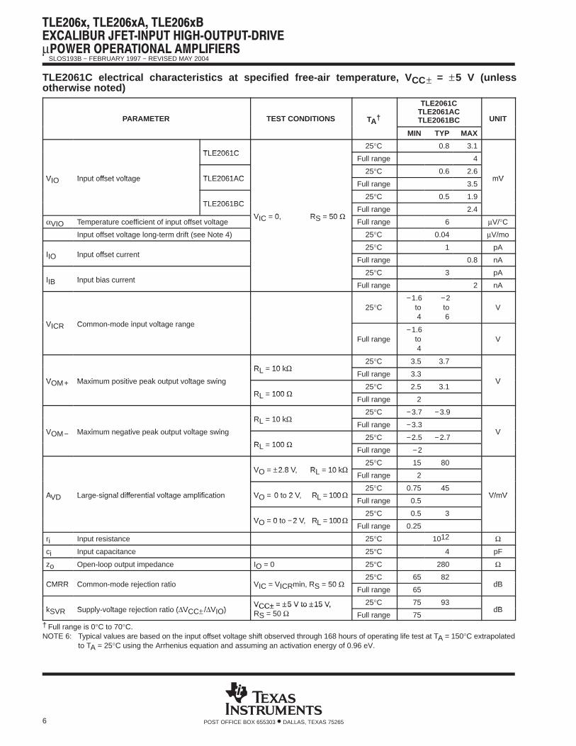
TLE2061C electrical characteristics at specified free-air temperature, V CC± = ±5 V (unlessotherwise noted)
PARAMETER TEST CONDITIONS TA†
TLE2061CTLE2061ACTLE2061BC UNITTA
MIN TYP MAX
TLE2061C25°C 0.8 3.1
TLE2061CFull range 4
VIO Input offset voltage TLE2061AC25°C 0.6 2.6
mVVIO Input offset voltage TLE2061ACFull range 3.5
mV
TLE2061BC25°C 0.5 1.9
TLE2061BC
VIC = 0, RS = 50 ΩFull range 2.4
αVIO Temperature coefficient of input offset voltageVIC = 0, RS = 50 Ω
Full range 6 µV/°C
Input offset voltage long-term drift (see Note 4) 25°C 0.04 µV/mo
IIO Input offset current25°C 1 pA
IIO Input offset currentFull range 0.8 nA
IIB Input bias current25°C 3 pA
IIB Input bias currentFull range 2 nA
VICR Common-mode input voltage range
25°C−1.6
to4
−2to6
V
VICR Common-mode input voltage range
Full range−1.6
to4
V
RL = 10 kΩ25°C 3.5 3.7
VOM+ Maximum positive peak output voltage swing
RL = 10 kΩFull range 3.3
VVOM+ Maximum positive peak output voltage swing
RL = 100 Ω25°C 2.5 3.1
V
RL = 100 ΩFull range 2
RL = 10 kΩ25°C −3.7 −3.9
VOM− Maximum negative peak output voltage swing
RL = 10 kΩFull range −3.3
VVOM− Maximum negative peak output voltage swing
RL = 100 Ω25°C −2.5 −2.7
V
RL = 100 ΩFull range −2
VO = ±2.8 V, RL = 10 kΩ25°C 15 80
VO = ±2.8 V, RL = 10 kΩFull range 2
AVD Large-signal differential voltage amplification VO = 0 to 2 V, RL = 100 Ω25°C 0.75 45
V/mVAVD Large-signal differential voltage amplification VO = 0 to 2 V, RL = 100 ΩFull range 0.5
V/mV
VO = 0 to −2 V, RL = 100 Ω25°C 0.5 3
VO = 0 to −2 V, RL = 100 ΩFull range 0.25
ri Input resistance 25°C 1012 Ω
ci Input capacitance 25°C 4 pF
zo Open-loop output impedance IO = 0 25°C 280 Ω
CMRR Common-mode rejection ratio VIC = VICRmin, RS = 50 Ω25°C 65 82
dBCMRR Common-mode rejection ratio VIC = VICRmin, RS = 50 ΩFull range 65
dB
kSVR Supply-voltage rejection ratio (∆VCC /∆VIO)VCC± = ±5 V to ±15 V, 25°C 75 93
dBkSVR Supply-voltage rejection ratio (∆VCC± /∆VIO)VCC± = ±5 V to ±15 V,RS = 50 Ω Full range 75
dB
† Full range is 0°C to 70°C.NOTE 6: Typical values are based on the input offset voltage shift observed through 168 hours of operating life test at TA = 150°C extrapolated
to TA = 25°C using the Arrhenius equation and assuming an activation energy of 0.96 eV.

µ
SLOS193B − FEBRUARY 1997 − REVISED MAY 2004
7POST OFFICE BOX 655303 • DALLAS, TEXAS 75265
TLE2061C electrical characteristics at specified free-air temperature, V CC± = ±5 V (unlessotherwise noted) (continued)
PARAMETER TEST CONDITIONS TA†
TLE2061CTLE2061ACTLE2061BC UNITTA
MIN TYP MAX
ICC Supply current25°C 280 325
AICC Supply currentVO = 0, No load Full range 350
µA
∆ICC Supply-current change over operating temperature range
VO = 0, No load
Full range 29 µA
† Full range is 0°C to 70°C.
TLE2061C operating characteristics at specified free-air temperature, V CC± = ±5 V
PARAMETER TEST CONDITIONS TA†
TLE2061CTLE2061ACTLE2061BC UNITPARAMETER TEST CONDITIONS TA
MIN TYP MAX
UNIT
SR Slew rate at unity gain (see Figure 1) RL = 10 kΩ, CL = 100 pF25°C 2.2 3.4
V/ sSR Slew rate at unity gain (see Figure 1) RL = 10 kΩ, CL = 100 pFFull range 2.1
V/µs
Vn Equivalent input noise voltage (see Figure 2)f = 10 Hz, RS = 20 Ω
25°C59 100
nV/√HzVn Equivalent input noise voltage (see Figure 2)f = 1 kHz , RS = 20 Ω
25°C43 60
nV/√Hz
VN(PP) Peak-to-peak equivalent input noise voltage f = 0.1 Hz to 10 Hz 25°C 1.1 VVN(PP) Peak-to-peak equivalent input noise voltage f = 0.1 Hz to 10 Hz 25°C 1.1 µV
In Equivalent input noise current f = 1 kHz 25°C 1 fA/√Hz
THD Total harmonic distortionAVD = 2, f = 10 kHz,
25°C 0.025%THD Total harmonic distortionAVD = 2, f = 10 kHz,VO(PP) = 2 V, RL = 10 kΩ 25°C 0.025%
B1 Unity-gain bandwidth (see Figure 3)RL = 10 kΩ, CL = 100 pF
25°C1.8
MHzB1 Unity-gain bandwidth (see Figure 3)RL = 100 Ω, CL = 100 pF
25°C1.3
MHz
ts Settling time0.1%
25°C5
sts Settling time0.01%
25°C10
µs
BOM Maximum output-swing bandwidth AVD = 1, RL = 10 kΩ 25°C 140 kHz
φm Phase margin at unity gain (see Figure 3)RL = 10 kΩ, CL = 100 pF
25°C58°
φm Phase margin at unity gain (see Figure 3)RL = 100 Ω, CL = 100 pF
25°C75°
† Full range is 0°C to 70°C.

µ
SLOS193B − FEBRUARY 1997 − REVISED MAY 2004
8 POST OFFICE BOX 655303 • DALLAS, TEXAS 75265
TLE2061C electrical characteristics at specified free-air temperature, V CC± = ±15 V (unlessotherwise noted)
PARAMETER TEST CONDITIONS TA†
TLE2061CTLE2061ACTLE2061BC UNITTA
MIN TYP MAX
TLE2061C25°C 0.6 3
TLE2061CFull range 3.9
VIO Input offset voltage TLE2061AC25°C 0.5 1.5
mVVIO Input offset voltage TLE2061ACFull range 2.5
mV
TLE2061BC25°C 0.3 0.5
TLE2061BC
VIC = 0, RS = 50 kΩFull range 1
αVIO Temperature coefficient of input offset voltageVIC = 0, RS = 50 kΩ
Full range 6 µV/°C
Input offset voltage long-term drift (see Note 4) 25°C 0.04 µV/mo
IIO Input offset current25°C 2 pA
IIO Input offset currentFull range 1 nA
IIB Input bias current25°C 4 pA
IIB Input bias currentFull range 3 nA
VICR Common-mode input voltage range
25°C−11
to13
−12to16
V
VICR Common-mode input voltage range
Full range−11
to13
V
RL = 10 kΩ25°C 13.2 13.7
VOM+ Maximum positive peak output voltage swing
RL = 10 kΩFull range 13
VVOM+ Maximum positive peak output voltage swing
RL = 600 Ω25°C 12.5 13.2
V
RL = 600 ΩFull range 12
RL = 10 kΩ25°C −13.2 −13.7
VOM− Maximum negative peak output voltage swing
RL = 10 kΩFull range −13
VVOM− Maximum negative peak output voltage swing
RL = 600 Ω25°C −12.5 −13
V
RL = 600 ΩFull range −12
VO = ±10 V, RL = 10 kΩ25°C 30 230
VO = ±10 V, RL = 10 kΩFull range 20
AVD Large-signal differential voltage amplification VO = 0 to 8 V, RL = 600 Ω25°C 25 100
V/mVAVD Large-signal differential voltage amplification VO = 0 to 8 V, RL = 600 ΩFull range 10
V/mV
VO = 0 to −8 V, RL = 600 Ω25°C 3 25
VO = 0 to −8 V, RL = 600 ΩFull range 1
ri Input resistance 25°C 1012 Ω
ci Input capacitance 25°C 4 pF
zo Open-loop output impedance IO = 0 25°C 280 Ω
CMRR Common-mode rejection ratio VIC = VICRmin, RS = 50 Ω25°C 72 90
dBCMRR Common-mode rejection ratio VIC = VICRmin, RS = 50 ΩFull range 70
dB
kSVR Supply-voltage rejection ratio (∆VCC /∆VIO)VCC± = ±5 V to ±15 V, 25°C 75 93
dBkSVR Supply-voltage rejection ratio (∆VCC± /∆VIO)VCC± = ±5 V to ±15 V,RS = 50 Ω Full range 75
dB
† Full range is 0°C to 70°C.NOTE 4: Typical values are based on the input offset voltage shift observed through 168 hours of operating life test at TA = 150°C extrapolated
to TA = 25°C using the Arrhenius equation and assuming an activation energy of 0.96 eV.

µ
SLOS193B − FEBRUARY 1997 − REVISED MAY 2004
9POST OFFICE BOX 655303 • DALLAS, TEXAS 75265
TLE2061C electrical characteristics at specified free-air temperature, V CC ± = ±15 V (unlessotherwise noted) (continued)
PARAMETER TEST CONDITIONS TA†
TLE2061CTLE2061ACTLE2061BC UNITTA
MIN TYP MAX
ICC Supply current25°C 290 350
AICC Supply currentVO = 0, No load Full range 375
µA
∆ICC Supply-current change over operating temperature range
VO = 0, No load
Full range 34 µA∆ICC Supply-current change over operating temperature range Full range 34 µA† Full range is 0°C to 70°C.
TLE2061C operating characteristics at specified free-air temperature, V CC± = ±15 V
PARAMETER TEST CONDITIONS TA†
TLE2061CTLE2061ACTLE2061BC UNITTA
MIN TYP MAX
SR Slew rate at unity gain (see Figure 1) RL = 10 kΩ, CL = 100 pF25°C 2.6 3.4
V/ sSR Slew rate at unity gain (see Figure 1) RL = 10 kΩ, CL = 100 pFFull range 2.5
V/µs
Vn Equivalent input noise voltage (see Figure 2)f = 10 Hz, RS = 20 Ω
25°C70 100
nV/√HzVn Equivalent input noise voltage (see Figure 2)f = 1 kHz , RS = 20 Ω
25°C40 60
nV/√Hz
VN(PP) Peak-to-peak equivalent input noise voltage f = 0.1 Hz to 10 Hz 25°C 1.1 µV
In Equivalent input noise current f = 1 kHz 25°C 1.1 fA/√Hz
THD Total harmonic distortionAVD = 2, f = 10 kHz,
25°C 0.025%THD Total harmonic distortionAVD = 2, f = 10 kHz,VO(PP) = 2 V, RL = 10 kΩ 25°C 0.025%
B1 Unity-gain bandwidth (see Figure 3)RL = 10 kΩ, CL = 100 pF
25°C2
MHzB1 Unity-gain bandwidth (see Figure 3)RL = 600 Ω, CL = 100 pF
25°C1.5
MHz
ts Settling time0.1%
25°C5
sts Settling time0.01%
25°C10
µs
BOM Maximum output-swing bandwidth AVD = 1, RL = 10 kΩ 25°C 40 kHz
φm Phase margin at unity gain (see Figure 3)RL = 10 kΩ, CL = 100 pF
25°C60°
φm Phase margin at unity gain (see Figure 3)RL = 600 Ω, CL = 100 pF
25°C70°
† Full range is 0°C to 70°C.
µ
SLOS193B − FEBRUARY 1997 − REVISED MAY 2004
10 POST OFFICE BOX 655303 • DALLAS, TEXAS 75265
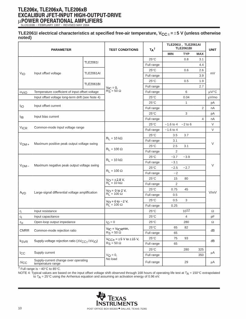
TLE2061I electrical characteristics at specified free-air temperature, V CC± = ±5 V (unless otherwisenoted)
PARAMETER TEST CONDITIONS TA†TLE2061I , TLE2061AI
TLE2061BI UNITPARAMETER TEST CONDITIONS TA†
MIN TYP MAXUNIT
TLE2061I25°C 0.8 3.1
TLE2061IFull range 4.4
VIO Input offset voltage TLE2061AI25°C 0.6 2.6
mVVIO Input offset voltage TLE2061AIFull range 3.9
mV
TLE2061BI25°C 0.5 1.9
TLE2061BIVIC = 0,R = 50
Full range 2.7
αVIO Temperature coefficient of input offset voltageVIC = 0,RS = 50 Ω Full range 6 µV/°C
Input offset voltage long-term drift (see Note 4)
S
25°C 0.04 µV/mo
IIO Input offset current25°C 1 pA
IIO Input offset currentFull range 2 nA
IIB Input bias current25°C 3 pA
IIB Input bias currentFull range 4 nA
VICR Common-mode input voltage range25°C −1.6 to 4 −2 to 6 V
VICR Common-mode input voltage rangeFull range −1.6 to 4 V
RL = 10 kΩ25°C 3.5 3.7
VOM+ Maximum positive peak output voltage swing
RL = 10 kΩFull range 3.1
VVOM+ Maximum positive peak output voltage swing
RL = 100 Ω25°C 2.5 3.1
V
RL = 100 ΩFull range 2
RL = 10 kΩ25°C −3.7 −3.9
VOM− Maximum negative peak output voltage swing
RL = 10 kΩFull range −3.1
VVOM− Maximum negative peak output voltage swing
RL = 100 Ω25°C −2.5 −2.7
V
RL = 100 ΩFull range −2
VO = ±2.8 V,R = 10 k
25°C 15 80VO = ±2.8 V,RL = 10 kΩ Full range 2
AVD Large-signal differential voltage amplificationVO = 0 to 2 V,R = 100
25°C 0.75 45V/mVAVD Large-signal differential voltage amplification
VO = 0 to 2 V,RL = 100 Ω Full range 0.5
V/mV
VO = 0 to −2 V,R = 100
25°C 0.5 3VO = 0 to −2 V,RL = 100 Ω Full range 0.25
ri Input resistance 25°C 1012 Ω
ci Input capacitance 25°C 4 pF
zo Open-loop output impedance IO = 0 25°C 280 Ω
CMRR Common-mode rejection ratioVIC = VICRmin, 25°C 65 82
dBCMRR Common-mode rejection ratioVIC = VICRmin,RS = 50 Ω Full range 65
dB
kSVR Supply-voltage rejection ratio (∆VCC /∆VIO)VCC± = ±5 V to ±15 V, 25°C 75 93
dBkSVR Supply-voltage rejection ratio (∆VCC± /∆VIO)VCC± = ±5 V to ±15 V,RS = 50 Ω Full range 65
dB
ICC Supply current25°C 280 325
AICC Supply currentVO = 0, No load
Full range 350µA
∆ICCSupply-current change over operating temperature range
VO = 0, No load
Full range 29 µA
† Full range is −40°C to 85°C.NOTE 4: Typical values are based on the input offset voltage shift observed through 168 hours of operating life test at TA = 150°C extrapolated
to TA = 25°C using the Arrhenius equation and assuming an activation energy of 0.96 eV.
µ
SLOS193B − FEBRUARY 1997 − REVISED MAY 2004
11POST OFFICE BOX 655303 • DALLAS, TEXAS 75265
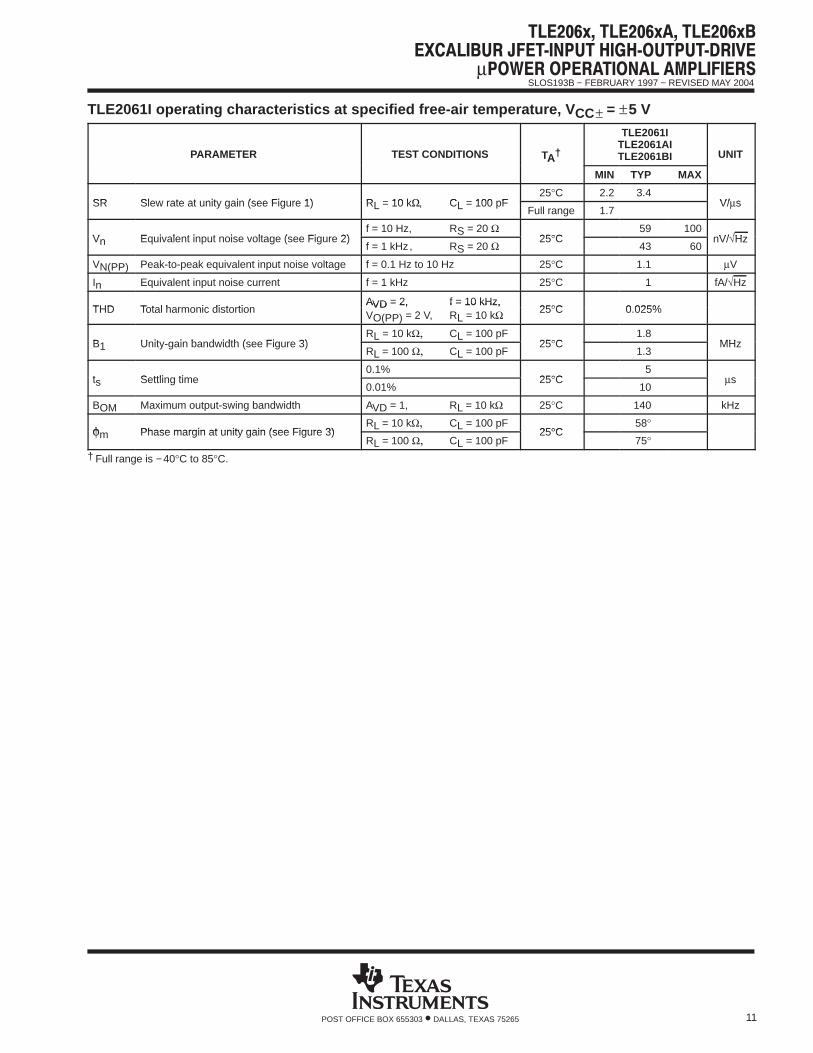
TLE2061I operating characteristics at specified free-air temperature, V CC± = ±5 V
PARAMETER TEST CONDITIONS TA†
TLE2061ITLE2061AITLE2061BI UNITTA
MIN TYP MAX
SR Slew rate at unity gain (see Figure 1) RL = 10 kΩ, CL = 100 pF25°C 2.2 3.4
V/ sSR Slew rate at unity gain (see Figure 1) RL = 10 kΩ, CL = 100 pFFull range 1.7
V/µs
Vn Equivalent input noise voltage (see Figure 2)f = 10 Hz, RS = 20 Ω
25°C59 100
nV/√HzVn Equivalent input noise voltage (see Figure 2)f = 1 kHz , RS = 20 Ω
25°C43 60
nV/√Hz
VN(PP) Peak-to-peak equivalent input noise voltage f = 0.1 Hz to 10 Hz 25°C 1.1 µV
In Equivalent input noise current f = 1 kHz 25°C 1 fA/√Hz
THD Total harmonic distortionAVD = 2, f = 10 kHz,
25°C 0.025%THD Total harmonic distortionAVD = 2, f = 10 kHz,VO(PP) = 2 V, RL = 10 kΩ 25°C 0.025%
B1 Unity-gain bandwidth (see Figure 3)RL = 10 kΩ, CL = 100 pF
25°C1.8
MHzB1 Unity-gain bandwidth (see Figure 3)RL = 100 Ω, CL = 100 pF
25°C1.3
MHz
ts Settling time0.1%
25°C5
sts Settling time0.01%
25°C10
µs
BOM Maximum output-swing bandwidth AVD = 1, RL = 10 kΩ 25°C 140 kHz
φm Phase margin at unity gain (see Figure 3)RL = 10 kΩ, CL = 100 pF
25°C58°
φm Phase margin at unity gain (see Figure 3)RL = 100 Ω, CL = 100 pF
25°C75°
† Full range is −40°C to 85°C.

µ
SLOS193B − FEBRUARY 1997 − REVISED MAY 2004
12 POST OFFICE BOX 655303 • DALLAS, TEXAS 75265
TLE2061I electrical characteristics at specified free-air temperature, V CC± = ±15 V (unlessotherwise noted)
PARAMETER TEST CONDITIONS TA†TLE2061I, TLE2061AI
TLE2061BI UNITPARAMETER TEST CONDITIONS TA†
MIN TYP MAXUNIT
TLE2061I25°C 0.6 3
TLE2061IFull range 4.3
VIO Input offset voltage TLE2061AI25°C 0.5 1.5
mVVIO Input offset voltage TLE2061AIFull range 2.9
mV
TLE2061BI25°C 0.3 0.5
TLE2061BIFull range 1.3
αVIOTemperature coefficient of input offset voltage
VIC = 0,RS = 50 Ω Full range 6 µV/°C
Input offset voltage long-term drift (see Note 4)
S
25°C 0.04 µV/mo
IIO Input offset current25°C 2 pA
IIO Input offset currentFull range 3 nA
IIB Input bias current25°C 4 pA
IIB Input bias currentFull range 5 nA
VICR Common-mode input voltage range25°C −11 to 13 −12 to 16 V
VICR Common-mode input voltage rangeFull range −11 to 13 V
RL = 10 kΩ25°C 13.2 13.7
VOM+ Maximum positive peak output voltage swing
RL = 10 kΩFull range 13
VVOM+ Maximum positive peak output voltage swing
RL = 600 Ω25°C 12.5 13.2
V
RL = 600 ΩFull range 12
RL = 10 kΩ25°C −13.2 −13.7
VOM−Maximum negative peak output voltageswing
RL = 10 kΩFull range −13
VVOM−Maximum negative peak output voltageswing
RL = 600 Ω25°C −12.5 −13
V
RL = 600 ΩFull range −12
VO = ±10 V,R = 10 k
25°C 30 230VO = ±10 V,RL = 10 kΩ Full range 20
AVD Large-signal differential voltage amplificationVO = 0 to 8 V,R = 600
25°C 25 100V/mVAVD Large-signal differential voltage amplification
VO = 0 to 8 V,RL = 600 Ω Full range 10
V/mV
VO = 0 to −8 V,R = 600
25°C 3 25VO = 0 to −8 V,RL = 600 Ω Full range 01
ri Input resistance 25°C 1012 Ω
ci Input capacitance 25°C 4 pF
zo Open-loop output impedance IO = 0 25°C 280 Ω
CMRR Common-mode rejection ratioVIC = VICRmin,R = 50
25°C 72 90dBCMRR Common-mode rejection ratio
VIC = VICRmin,RS = 50 Ω Full range 65
dB
kSVR Supply-voltage rejection ratio (∆VCC /∆VIO)VCC± = ±5 V to ±15 V, 25°C 75 93
dBkSVR Supply-voltage rejection ratio (∆VCC± /∆VIO)VCC± = ±5 V to ±15 V,RS = 50 Ω Full range 65
dB
ICC Supply current25°C 290 350
AICC Supply currentVO = 0, No load
Full range 375µA
∆ICCSupply-current change over operating temperature range
VO = 0, No load
Full range 34 µA
† Full range is −40°C to 85°C.NOTE 4: Typical values are based on the input offset voltage shift observed through 168 hours of operating life test at TA = 150°C extrapolated
to TA = 25°C using the Arrhenius equation and assuming an activation energy of 0.96 eV.

µ
SLOS193B − FEBRUARY 1997 − REVISED MAY 2004
13POST OFFICE BOX 655303 • DALLAS, TEXAS 75265
TLE2061I operating characteristics at specified free-air temperature, V CC± = ±15 V
PARAMETER TEST CONDITIONS TA†
TLE2061ITLE2061AITLE2061BI UNITTA
MIN TYP MAX
SR Slew rate at unity gain (see Figure 1) RL = 10 kΩ, CL = 100 pF25°C 2.6 3.4
V/ sSR Slew rate at unity gain (see Figure 1) RL = 10 kΩ, CL = 100 pFFull range 2.1
V/µs
Vn Equivalent input noise voltage (see Figure 2)f = 10 Hz, RS = 20 Ω
25°C70 100
nV/√HzVn Equivalent input noise voltage (see Figure 2)f = 1 kHz , RS = 20 Ω
25°C40 60
nV/√Hz
VN(PP) Peak-to-peak equivalent input noise voltage f = 0.1 Hz to 10 Hz 25°C 1.1 µV
In Equivalent input noise current f = 1 kHz 25°C 1.1 fA/√Hz
THD Total harmonic distortionAVD = 2, f = 10 kHz,
25°C 0.025%THD Total harmonic distortionAVD = 2, f = 10 kHz,VO(PP) = 2 V, RL = 10 kΩ 25°C 0.025%
B1 Unity-gain bandwidth (see Figure 3)RL = 10 kΩ, CL = 100 pF
25°C2
MHzB1 Unity-gain bandwidth (see Figure 3)RL = 600 Ω, CL = 100 pF
25°C1.5
MHz
ts Settling time0.1%
25°C5
sts Settling time0.01%
25°C10
µs
BOM Maximum output-swing bandwidth AVD = 1, RL = 10 kΩ 25°C 40 kHz
φm Phase margin at unity gain (see Figure 3)RL = 10 kΩ, CL = 100 pF
25°C60°
φm Phase margin at unity gain (see Figure 3)RL = 600 Ω, CL = 100 pF
25°C70°
† Full range is −40°C to 85°C.

µ
SLOS193B − FEBRUARY 1997 − REVISED MAY 2004
14 POST OFFICE BOX 655303 • DALLAS, TEXAS 75265
TLE2061M electrical characteristics at specified free-air temperature, V CC± = ±5 V (unlessotherwise noted)
PARAMETER TEST CONDITIONS TA†
TLE2061MTLE2061AMTLE2061BM UNITTA
MIN TYP MAX
TLE2061M25°C 0.8 3.1
TLE2061MFull range 6
VIO Input offset voltage TLE2061AM25°C 0.6 2.6
mVVIO Input offset voltage TLE2061AMFull range 4.6
mV
TLE2061BM25°C 0.5 1.9
TLE2061BM
VIC = 0, RS = 50 ΩFull range 3.1
αVIO Temperature coefficient of input offset voltageVIC = 0, RS = 50 Ω
Full range 6 µV/°C
Input offset voltage long-term drift (see Note 4) 25°C 0.04 µV/mo
IIO Input offset current25°C 1 pA
IIO Input offset currentFull range 15 nA
IIB Input bias current25°C 3 pA
IIB Input bias currentFull range 30 nA
VICR Common-mode input voltage range
25°C−1.6
to4
−2to6
V
VICR Common-mode input voltage range
Full range−1.6
to4
V
RL = 10 kΩ25°C 3.5 3.7
RL = 10 kΩFull range 3
VOM+ Maximum positive peak output voltage swing RL = 600 Ω25°C 2.5 3.6
VVOM+ Maximum positive peak output voltage swing RL = 600 ΩFull range 2
V
RL = 100 Ω25°C 2.5 3.1
RL = 100 ΩFull range 2
RL = 10 kΩ25°C −3.5 −3.9
RL = 10 kΩFull range −3
VOM−Maximum negative peak FK and JG
RL = 600 Ω25°C −2.5 −3.5
VVOM−Maximum negative peakoutput voltage swing
FK and JGpackages RL = 600 Ω
Full range −2Voutput voltage swing
D and PRL = 100 Ω
25°C −2.5 −2.7D and Ppackages RL = 100 Ω
Full range −2
VO = ±2.8 V, RL = 10 kΩ25°C 15 80
VO = ±2.8 V, RL = 10 kΩFull range 2
VO = 0 to 2.5 V, RL = 600 Ω25°C 1 65
FK and JGVO = 0 to 2.5 V, RL = 600 Ω
Full range 0.5
AVDLarge-signal differential
FK and JGpackages
VO = 0 to −2.5 V,RL = 600 Ω25°C 1 16
V/mVAVDLarge-signal differentialvoltage amplification
packagesVO = 0 to −2.5 V,RL = 600 Ω
Full range 0.5V/mV
voltage amplification
VO = 0 to 2 V, RL = 100 Ω25°C 0.75 45
D and PVO = 0 to 2 V, RL = 100 Ω
Full range 0.5D and Ppackages
VO = 0 to −2 V, RL = 100 Ω25°C 0.5 3packages
VO = 0 to −2 V, RL = 100 ΩFull range 0.25
† Full range is −55°C to 125°C.NOTE 4: Typical values are based on the input offset voltage shift observed through 168 hours of operating life test at TA = 150°C extrapolated
to TA = 25°C using the Arrhenius equation and assuming an activation energy of 0.96 eV.

µ
SLOS193B − FEBRUARY 1997 − REVISED MAY 2004
15POST OFFICE BOX 655303 • DALLAS, TEXAS 75265
TLE2061M electrical characteristics at specified free-air temperature, V CC± = ±5 V (unlessotherwise noted) (continued)
PARAMETER TEST CONDITIONS TA†
TLE2061MTLE2061AMTLE2061BM UNITTA
MIN TYP MAX
ri Input resistance 25°C 1012 Ω
ci Input capacitance 25°C 4 pF
zo Open-loop output impedance IO = 0 25°C 280 Ω
CMRR Common-mode rejection ratioVIC = VICRmin, 25°C 65 82
dBCMRR Common-mode rejection ratioVIC = VICRmin,RS = 50 Ω Full range 60
dB
kSVR Supply-voltage rejection ratio (∆VCC± /∆VIO)VCC± = ±5 V to ±15 V,R = 50
25°C 75 93dBkSVR Supply-voltage rejection ratio (∆VCC± /∆VIO)
VCC± = 5 V to 15 V,RS = 50 Ω Full range 65
dB
ICC Supply current25°C 280 325
AICC Supply currentVO = 0, No load
Full range 350µA
∆ICCSupply-current change over operatingtemperature range
VO = 0, No load
Full range 39 µA
† Full range is −55°C to 125°C.
TLE2061M operating characteristics at specified free-air temperature, V CC± = ±5 V, TA = 25°C
PARAMETER TEST CONDITIONS
TLE2061MTLE2061AMTLE2061BM UNIT
MIN TYP MAX
SR Slew rate at unity gain (see Figure 1) RL = 10 kΩ, CL = 100 pF 3.4 V/ sSR Slew rate at unity gain (see Figure 1) RL = 10 kΩ, CL = 100 pF 3.4 V/µs
Vn Equivalent input noise voltage (see Figure 2)f = 10 Hz, RS = 20 Ω 59
nV/√HzVn Equivalent input noise voltage (see Figure 2)f = 1 kHz , RS = 20 Ω 43
nV/√Hz
VN(PP) Peak-to-peak equivalent input noise voltage f = 0.1 Hz to 10 Hz 1.1 VVN(PP) Peak-to-peak equivalent input noise voltage f = 0.1 Hz to 10 Hz 1.1 µV
In Equivalent input noise current f = 1 kHz 1 fA /√Hz
THD Total harmonic distortionAVD = 2, f = 10 kHz,
0.025%THD Total harmonic distortionAVD = 2, f = 10 kHz,VO(PP) = 2 V, RL = 10 kΩ 0.025%
B1 Unity-gain bandwidth (see Figure 3)RL = 10 kΩ, CL = 100 pF 1.8
MHzB1 Unity-gain bandwidth (see Figure 3)RL = 600 Ω, CL = 100 pF 1.3
MHz
ts Settling time0.1% 5
sts Settling time0.01% 10
µs
BOM Maximum output-swing bandwidth AVD = 1, RL = 10 kΩ 140 kHz
φm Phase margin at unity gain (see Figure 3)RL = 10 kΩ, CL = 100 pF 58°
φm Phase margin at unity gain (see Figure 3)RL = 600 Ω, CL = 100 pF 75°

µ
SLOS193B − FEBRUARY 1997 − REVISED MAY 2004
16 POST OFFICE BOX 655303 • DALLAS, TEXAS 75265
TLE2061M electrical characteristics at specified free-air temperature, V CC± = ±15 V (unlessotherwise noted)
PARAMETER TEST CONDITIONS TA†TLE2061M ,TLE2061AM
TLE2061BM UNITPARAMETER TEST CONDITIONS TA†
MIN TYP MAXUNIT
TLE2061M25°C 0.6 3
TLE2061MFull range 6
VIO Input offset voltage TLE2061AM25°C 0.5 1.5
mVVIO Input offset voltage TLE2061AMFull range 3.6
mV
TLE2061BM25°C 0.3 0.5
TLE2061BMFull range 1.7
αVIOTemperature coefficient of input offsetvoltage
VIC = 0,RS = 50 Ω Full range 6 µV/°C
Input offset voltage long-term drift (see Note 4)
S
25°C 0.04 µV/mo
IIO Input offset current25°C 2 pA
IIO Input offset currentFull range 20 nA
IIB Input bias current25°C 4 pA
IIB Input bias currentFull range 40 nA
VICR Common-mode input voltage range25°C −11 to 13 −12 to 16 V
VICR Common-mode input voltage rangeFull range −11 to 13 V
RL = 10 kΩ25°C 13 13.7
VOM+Maximum positive peak output voltageswing
RL = 10 kΩFull range 12.5
VVOM+Maximum positive peak output voltageswing
RL = 600 Ω25°C 12.5 13.2
V
RL = 600 ΩFull range 12
RL = 10 kΩ25°C −13 −13.7
VOM−Maximum negative peak output voltageswing
RL = 10 kΩFull range −12.5
VVOM−Maximum negative peak output voltageswing
RL = 600 Ω25°C −12.5 −13
V
RL = 600 ΩFull range −12
VO = ±10 V,R = 10 k
25°C 30 230VO = ±10 V,RL = 10 kΩ Full range 20
AVDLarge-signal differential voltage amplification
VO = 0 to 8 V,R = 600
25°C 25 100V/mVAVD
Large-signal differential voltage amplification
VO = 0 to 8 V,RL = 600 Ω Full range 7
V/mV
VO = 0 to − 8 V,R = 600
25°C 3 25VO = 0 to − 8 V,RL = 600 Ω Full range 1
ri Input resistance 25°C 1012 Ω
ci Input capacitance 25°C 4 pF
zo Open-loop output impedance IO = 0 25°C 280 Ω
CMRR Common-mode rejection ratioVIC = VICRmin,R = 50
25°C 72 90dBCMRR Common-mode rejection ratio
VIC = VICRmin,RS = 50 Ω Full range 65
dB
kSVRSupply-voltage rejection ratio VCC± = ±5 V to ±15 V, 25°C 75 93
dBkSVRSupply-voltage rejection ratio(∆VCC± /∆VIO)
VCC± = ±5 V to ±15 V,RS = 50 Ω Full range 65
dB
† Full range is −55°C to 125°C.NOTE 4: Typical values are based on the input offset voltage shift observed through 168 hours of operating life test at TA = 150°C extrapolated
to TA = 25°C using the Arrhenius equation and assuming an activation energy of 0.96 eV.

µ
SLOS193B − FEBRUARY 1997 − REVISED MAY 2004
17POST OFFICE BOX 655303 • DALLAS, TEXAS 75265
TLE2061M electrical characteristics at specified free-air temperature, V CC± = ±15 V (unlessotherwise noted) (continue)
PARAMETER TEST CONDITIONS TA†TLE2061M ,TLE2061AM
TLE2061BM UNITPARAMETER TEST CONDITIONS TA†
MIN TYP MAXUNIT
ICC Supply current25°C 290 350
AICC Supply currentVO = 0, No load
Full range 375µA
∆ICCSupply-current change over operating temperature range
VO = 0, No load
Full range 46 µA
† Full range is −55°C to 125°C.
TLE2061M operating characteristics at specified free-air temperature, V CC± = ±15 V
PARAMETER TEST CONDITIONS TA†
TLE2061MTLE2061AMTLE2061BM UNITTA
MIN TYP MAX
SR Slew rate at unity gain (see Figure 1) RL = 10 kΩ, CL = 100 pF25°C 2 3.4
V/ sSR Slew rate at unity gain (see Figure 1) RL = 10 kΩ, CL = 100 pFFull range 1.8
V/µs
Vn Equivalent input noise voltage (see Figure 2)f = 10 Hz, RS = 20 Ω 25°C 70
nV/√HzVn Equivalent input noise voltage (see Figure 2)f = 1 kHz, RS = 20 Ω 25°C 40
nV/√Hz
VN(PP) Peak-to-peak equivalent input noise voltage f = 0.1 Hz to 10 Hz 25°C 1.1 VVN(PP) Peak-to-peak equivalent input noise voltage f = 0.1 Hz to 10 Hz 25°C 1.1 µV
In Equivalent input noise current f = 1 kHz 25°C 1.1 fA /√Hz
THD Total harmonic distortionAVD = 2, f = 10 kHz,VO(PP) = 2 V, RL = 10 kΩ 25°C 0.025%
B1 Unity-gain bandwidth (see Figure 3)RL = 10 kΩ, CL = 100 pF 25°C 2
MHzB1 Unity-gain bandwidth (see Figure 3)RL = 600 Ω, CL = 100 pF 25°C 1.5
MHz
ts Settling time0.1% 25°C 5
sts Settling time0.01% 25°C 10
µs
BOM Maximum output-swing bandwidth AVD = 1, RL = 10 kΩ 25°C 40 kHzBOM Maximum output-swing bandwidth AVD = 1, RL = 10 kΩ 25°C 40 kHz
φm Phase margin at unity gain (see Figure 3)RL = 10 kΩ, CL = 100 pF 25°C 60°
φm Phase margin at unity gain (see Figure 3)RL = 600 Ω, CL = 100 pF 25°C 70°
† Full range is −55°C to 125°C.

µ
SLOS193B − FEBRUARY 1997 − REVISED MAY 2004
18 POST OFFICE BOX 655303 • DALLAS, TEXAS 75265
TLE2061Y electrical characteristics at V CC± = ±15 V, TA = 25°C (unless otherwise noted)
PARAMETER TEST CONDITIONSTLE2061Y
UNITPARAMETER TEST CONDITIONSMIN TYP MAX
UNIT
VIO Input offset voltage 0.6 3 mV
αVIO Input offset voltage long-term drift (see Note 4)VIC = 0, RS = 50 Ω
0.04 µV/mo
IIO Input offset currentVIC = 0, RS = 50 Ω
2 pA
IIB Input bias current 4 pA
VICR Common-mode input voltage range−11
to13
−12to16
V
VOM+ Maximum positive peak output voltage swingRL = 10 kΩ 13.2 13.7
VVOM+ Maximum positive peak output voltage swingRL = 600 Ω 12.5 13.2
V
VOM− Maximum negative peak output voltage swingRL = 10 kΩ −13.2 −13.7
VVOM− Maximum negative peak output voltage swingRL = 600 Ω −12.5 − 13
V
VO = ±10 V, RL = 10 kΩ 30 230
AVD Large-signal differential voltage amplification VO = 0 to 8 V, RL = 600 Ω 25 100 V/mVAVD Large-signal differential voltage amplification
VO = 0 to − 8 V, RL = 600 Ω 3 25
V/mV
ri Input resistance 1012 Ω
ci Input capacitance 4 pF
zo Open-loop output impedance IO = 0 280 Ω
CMRR Common-mode rejection ratio RS = 50 Ω, VIC = VICRmin 72 90 dB
kSVR Supply-voltage rejection ratio (∆VCC/∆VIO)VCC± = ±5 V to ±15 V,R = 50 75 93 dBkSVR Supply-voltage rejection ratio (∆VCC/∆VIO)VCC± = ±5 V to ±15 V,RS = 50 Ω 75 93 dB
ICC Supply current VO = 0, No load 290 350 µA
NOTE 4: Typical values are based on the input offset voltage shift observed through 168 hours of operating life test at TA = 150°C extrapolatedto TA = 25°C using the Arrhenius equation and assuming an activation energy of 0.96 eV.
TLE2061Y operating characteristics at V CC± = ±15 V, TA = 25°C
PARAMETER TEST CONDITIONSTLE2061Y
UNITPARAMETER TEST CONDITIONSMIN TYP MAX
UNIT
SR Slew rate at unity gain (see Figure 1) RL = 10 kΩ, CL = 100 pF 2.6 3.4 V/µs
Vn Equivalent input noise voltage (see Figure 2)f = 10 Hz, RS = 20 Ω 70
nV/√HzVn Equivalent input noise voltage (see Figure 2)f = 1 kHz , RS = 20 Ω 40
nV/√Hz
VN(PP) Peak-to-peak equivalent input noise voltage f = 0.1 Hz to 10 Hz 1.1 µV
In Equivalent input noise current f = 1 Hz 1.1 fA /√Hz
THD Total harmonic distortionAVD = 2, f = 10 kHz,
0.025%THD Total harmonic distortionAVD = 2, f = 10 kHz,VO(PP) = 2 V, RL = 10 kΩ 0.025%
B1 Unity-gain bandwidth (see Figure 3)RL = 10 kΩ, CL = 100 pF 2
MHzB1 Unity-gain bandwidth (see Figure 3)RL = 600 Ω, CL = 100 pF 1.5
MHz
ts Settling time0.1% 5
sts Settling time0.01% 10
µs
BOM Maximum output-swing bandwidth AVD = 1, RL = 10 kΩ 40 kHz
φm Phase margin at unity gain (see Figure 3)RL = 10 kΩ, CL = 100 pF 60°
φm Phase margin at unity gain (see Figure 3)RL = 600 Ω, CL = 100 pF 70°

µ
SLOS193B − FEBRUARY 1997 − REVISED MAY 2004
19POST OFFICE BOX 655303 • DALLAS, TEXAS 75265
TLE2062C electrical characteristics at specified free-air temperature, V CC± = ±5 V (unlessotherwise noted)
PARAMETER TEST CONDITIONS TA†
TLE2062CTLE2062ACTLE2062BC UNITA
MIN TYP MAX
TLE2062C25°C 1 5
TLE2062CFull range 5.9
VIO Input offset voltage TLE2062AC25°C 0.9 4
mVVIO Input offset voltage TLE2062ACFull range 4.9
mV
TLE2062BC25°C 0.7 3
TLE2062BC
VIC = 0, RS = 50 ΩFull range 3.9
αVIO Temperature coefficient of input offset voltageVIC = 0, RS = 50 Ω
Full range 6 µV/°C
Input offset voltage long-term drift (see Note 4) 25°C 0.04 µV/mo
IIO Input offset current25°C 1 pA
IIO Input offset currentFull range 0.8 nA
IIB Input bias current25°C 3 pA
IIB Input bias currentFull range 2 nA
VICR Common-mode input voltage range
25°C−1.6
to4
−2to6
V
VICR Common-mode input voltage range
Full range−1.6
to4
V
RL = 10 kΩ25°C 3.5 3.7
VOM+ Maximum positive peak output voltage swing
RL = 10 kΩFull range 3.3
VVOM+ Maximum positive peak output voltage swing
RL = 100 Ω25°C 2.5 3.1
V
RL = 100 ΩFull range 2
RL = 10 kΩ25°C −3.7 −3.9
VOM− Maximum negative peak output voltage swing
RL = 10 kΩFull range −3.3
VVOM− Maximum negative peak output voltage swing
RL = 100 Ω25°C −2.5 −2.7
V
RL = 100 ΩFull range −2
VO = ± 2.8 V, RL = 10 kΩ25°C 15 80
VO = ± 2.8 V, RL = 10 kΩFull range 2
AVD Large-signal differential voltage amplification VO = 0 to 2 V, RL = 100 Ω25°C 0.75 45
V/mVAVD Large-signal differential voltage amplification VO = 0 to 2 V, RL = 100 ΩFull range 0.5
V/mV
VO = 0 to −2 V, RL = 100 Ω25°C 0.5 3
VO = 0 to −2 V, RL = 100 ΩFull range 0.25
ri Input resistance 25°C 1012 Ω
ci Input capacitance 25°C 4 pF
zo Open-loop output impedance IO = 0 25°C 560 Ω
CMRR Common-mode rejection ratio VIC = VICRmin, RS = 50 Ω25°C 65 82
dBCMRR Common-mode rejection ratio VIC = VICRmin, RS = 50 ΩFull range 65
dB
kSVR Supply-voltage rejection ratio (∆VCC /∆VIO)VCC± = ± 5 V to ± 15 V, 25°C 75 93
dBkSVR Supply-voltage rejection ratio (∆VCC± /∆VIO)VCC± = ± 5 V to ± 15 V,RS = 50 Ω Full range 75
dB
† Full range is 0°C to 70°C.NOTE 4: Typical values are based on the input offset voltage shift observed through 168 hours of operating life test at TA = 150 °C extrapolated
to TA = 25 °C using the Arrhenius equation and assuming an activation energy of 0.96 eV.
µ
SLOS193B − FEBRUARY 1997 − REVISED MAY 2004
20 POST OFFICE BOX 655303 • DALLAS, TEXAS 75265
TLE2062C electrical characteristics at specified free-air temperature, V CC± = ±5 V (unlessotherwise noted) (continued)
PARAMETER TEST CONDITIONS TA†
TLE2062CTLE2062ACTLE2062BC UNITA
MIN TYP MAX
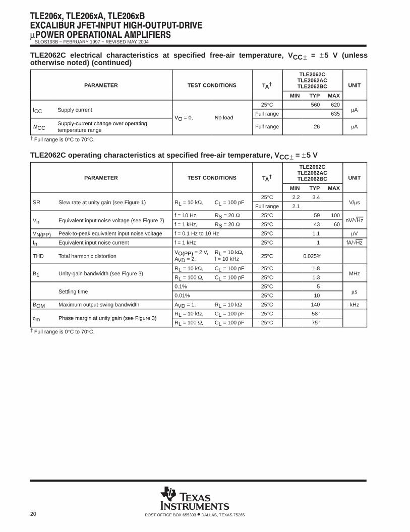
ICC Supply current25°C 560 620
AICC Supply currentVO = 0, No load
Full range 635µA
∆ICCSupply-current change over operating
VO = 0, No load
Full range 26 µA∆ICCSupply-current change over operatingtemperature range
Full range 26 µA
† Full range is 0°C to 70°C.
TLE2062C operating characteristics at specified free-air temperature, V CC± = ±5 V
PARAMETER TEST CONDITIONS TA†
TLE2062CTLE2062ACTLE2062BC UNITA
MIN TYP MAX
SR Slew rate at unity gain (see Figure 1) RL = 10 kΩ, CL = 100 pF25°C 2.2 3.4
V/ sSR Slew rate at unity gain (see Figure 1) RL = 10 kΩ, CL = 100 pFFull range 2.1
V/µs
Vn Equivalent input noise voltage (see Figure 2)f = 10 Hz, RS = 20 Ω 25°C 59 100
nV/√HzVn Equivalent input noise voltage (see Figure 2)f = 1 kHz, RS = 20 Ω 25°C 43 60
nV/√Hz
VN(PP) Peak-to-peak equivalent input noise voltage f = 0.1 Hz to 10 Hz 25°C 1.1 µV
In Equivalent input noise current f = 1 kHz 25°C 1 fA/√Hz
THD Total harmonic distortionVO(PP) = 2 V, RL = 10 kΩ,
25°C 0.025%THD Total harmonic distortionVO(PP) = 2 V,AVD = 2,
RL = 10 kΩ,f = 10 kHz 25°C 0.025%
B1 Unity-gain bandwidth (see Figure 3)RL = 10 kΩ, CL = 100 pF 25°C 1.8
MHzB1 Unity-gain bandwidth (see Figure 3)RL = 100 Ω, CL = 100 pF 25°C 1.3
MHz
Settling time0.1% 25°C 5
sSettling time0.01% 25°C 10
µs
BOM Maximum output-swing bandwidth AVD = 1, RL = 10 kΩ 25°C 140 kHz
φm Phase margin at unity gain (see Figure 3)RL = 10 kΩ, CL = 100 pF 25°C 58°
φm Phase margin at unity gain (see Figure 3)RL = 100 Ω, CL = 100 pF 25°C 75°
† Full range is 0°C to 70°C.

µ
SLOS193B − FEBRUARY 1997 − REVISED MAY 2004
21POST OFFICE BOX 655303 • DALLAS, TEXAS 75265
TLE2062C electrical characteristics at specified free-air temperature, V CC± = ±15 V (unlessotherwise noted)
PARAMETER TEST CONDITIONS TA†
TLE2062CTLE2062ACTLE2062BC UNITA
MIN TYP MAX
TLE2062C25°C 0.9 4
TLE2062CFull range 4.9
VIO Input offset voltage TLE2062AC25°C 0.8 2
mVVIO Input offset voltage TLE2062ACFull range 2.9
mV
TLE2062BC25°C 0.5 1
TLE2062BC
VIC = 0, RS = 50 ΩFull range 1.9
αVIO Temperature coefficient of input offset voltageVIC = 0, RS = 50 Ω
Full range 6 µV/°C
Input offset voltage long-term drift (see Note 4) 25°C 0.04 µV/mo
IIO Input offset current25°C 2 pA
IIO Input offset currentFull range 1 nA
IIB Input bias current25°C 4 pA
IIB Input bias currentFull range 3 nA
VICR Common-mode input voltage range
25°C−11
to13
−12to16
V
VICR Common-mode input voltage range
Full range−11
to13
V
RL = 10 kΩ25°C 13.2 13.7
VOM+ Maximum positive peak output voltage swing
RL = 10 kΩFull range 13
VVOM+ Maximum positive peak output voltage swing
RL = 600 Ω25°C 12.5 13.2
V
RL = 600 ΩFull range 12
RL = 10 kΩ25°C −13.2 −13.7
VOM− Maximum negative peak output voltage swing
RL = 10 kΩFull range −13
VVOM− Maximum negative peak output voltage swing
RL = 600 Ω25°C −12.5 −13
V
RL = 600 ΩFull range −12
VO = ± 10 V, RL = 10 kΩ25°C 30 230
VO = ± 10 V, RL = 10 kΩFull range 20
AVD Large-signal differential voltage amplification VO = 0 to 8 V, RL = 600 Ω25°C 25 100
V/mVAVD Large-signal differential voltage amplification VO = 0 to 8 V, RL = 600 ΩFull range 10
V/mV
VO = 0 to −8 V, RL = 600 Ω25°C 3 25
VO = 0 to −8 V, RL = 600 ΩFull range 1
ri Input resistance 25°C 1012 Ω
ci Input capacitance 25°C 4 pF
zo Open-loop output impedance IO = 0 25°C 560 Ω
CMRR Common-mode rejection ratio VIC = VICRmin, RS = 50 Ω25°C 72 90
dBCMRR Common-mode rejection ratio VIC = VICRmin, RS = 50 ΩFull range 70
dB
kSVR Supply-voltage rejection ratio (∆VCC /∆VIO)VCC± = ± 5 V to ± 15 V, 25°C 75 93
dBkSVR Supply-voltage rejection ratio (∆VCC± /∆VIO)VCC± = ± 5 V to ± 15 V,RS = 50 Ω Full range 75
dB
† Full range is 0°C to 70°C.NOTE 4: Typical values are based on the input offset voltage shift observed through 168 hours of operating life test at TA = 150 °C extrapolated
to TA = 25 °C using the Arrhenius equation and assuming an activation energy of 0.96 eV.

µ
SLOS193B − FEBRUARY 1997 − REVISED MAY 2004
22 POST OFFICE BOX 655303 • DALLAS, TEXAS 75265
TLE2062C electrical characteristics at specified free-air temperature, V CC± = ±15 V (unlessotherwise noted) (continued)
PARAMETER TEST CONDITIONS TA†
TLE2062CTLE2062ACTLE2062BC UNITA
MIN TYP MAX
ICC Supply current25°C 625 690
AICC Supply current
VO = 0 V, No loadFull range 715
µA
∆ICCSupply-current change over operating
VO = 0 V, No load
Full range 36 A∆ICCSupply-current change over operatingtemperature range Full range 36 µA
† Full range is 0°C to 70°C.
TLE2062C operating characteristics at specified free-air temperature, V CC± = ±15 V
PARAMETER TEST CONDITIONS TA†
TLE2062CTLE2062ACTLE2062BC UNITA
MIN TYP MAX
SR Slew rate at unity gain (see Figure 1) RL = 10 kΩ, CL = 100 pF25°C 2.6 3.4
V/ sSR Slew rate at unity gain (see Figure 1) RL = 10 kΩ, CL = 100 pFFull range 2.5
V/µs
Vn Equivalent input noise voltage (see Figure 2)f = 10 Hz, RS = 20 Ω 25°C 70 100
nV/√HzVn Equivalent input noise voltage (see Figure 2)f = 1 kHz, RS = 20 Ω 25°C 40 60
nV/√Hz
VN(PP) Peak-to-peak equivalent input noise voltage f = 0.1 Hz to 10 Hz 25°C 1.1 µV
In Equivalent input noise current f = 1 kHz 25°C 1.1 fA/√Hz
THD Total harmonic distortionVO(PP) = 2 V, RL = 10 kΩ,
25°C 0.025%THD Total harmonic distortionVO(PP) = 2 V,AVD = 2,
RL = 10 kΩ,f = 10 kHz 25°C 0.025%
B1 Unity-gain bandwidth (see Figure 3)RL = 10 kΩ, CL = 10 0 pF 25°C 2
MHzB1 Unity-gain bandwidth (see Figure 3)RL = 600 Ω, CL = 100 pF 25°C 1.5
MHz
Settling time0.1% 25°C 5
sSettling time0.01% 25°C 10
µs
BOM Maximum output-swing bandwidth AVD = 1, RL = 10 kΩ 25°C 40 kHz
φm Phase margin at unity gain (see Figure 3)RL = 10 kΩ, CL = 100 pF 25°C 60°
φm Phase margin at unity gain (see Figure 3)RL = 600 Ω, CL = 100 pF 25°C 70°
† Full range is 0°C to 70°C.
µ
SLOS193B − FEBRUARY 1997 − REVISED MAY 2004
23POST OFFICE BOX 655303 • DALLAS, TEXAS 75265
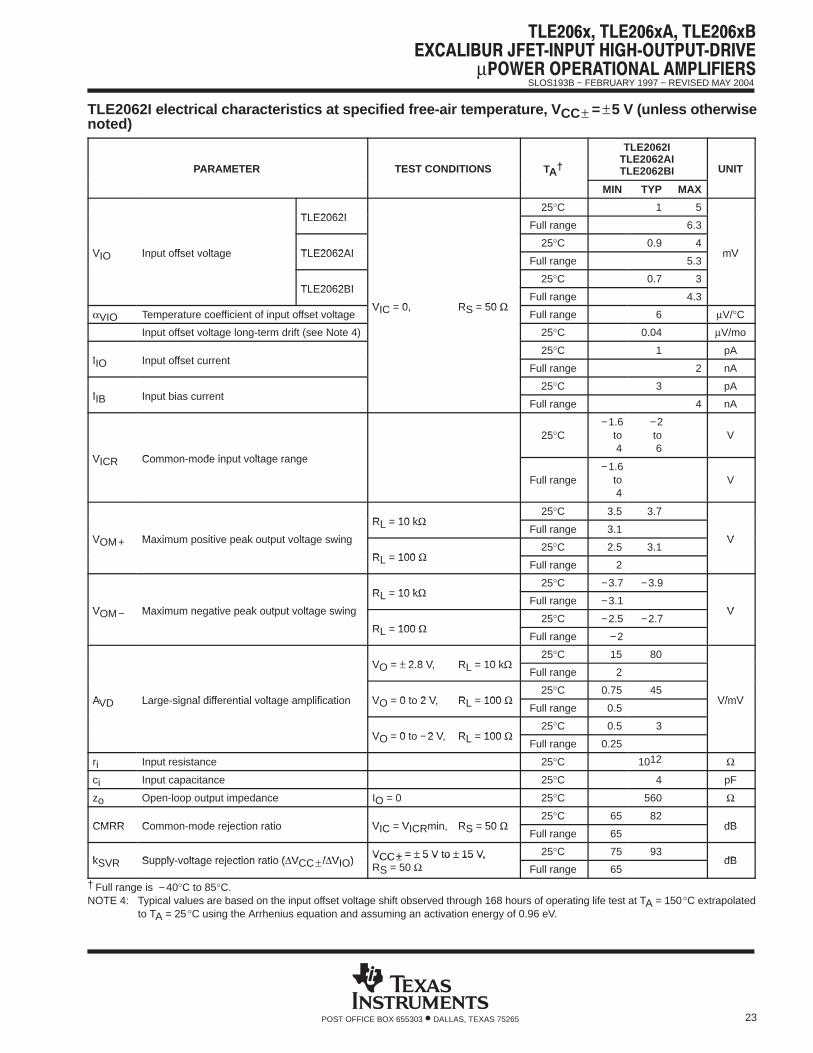
TLE2062I electrical characteristics at specified free-air temperature, V CC± = ±5 V (unless otherwisenoted)
PARAMETER TEST CONDITIONS TA†
TLE2062ITLE2062AITLE2062BI UNITA
MIN TYP MAX
TLE2062I25°C 1 5
TLE2062IFull range 6.3
VIO Input offset voltage TLE2062AI25°C 0.9 4
mVVIO Input offset voltage TLE2062AIFull range 5.3
mV
TLE2062BI25°C 0.7 3
TLE2062BI
VIC = 0, RS = 50 ΩFull range 4.3
αVIO Temperature coefficient of input offset voltageVIC = 0, RS = 50 Ω
Full range 6 µV/°C
Input offset voltage long-term drift (see Note 4) 25°C 0.04 µV/mo
IIO Input offset current25°C 1 pA
IIO Input offset currentFull range 2 nA
IIB Input bias current25°C 3 pA
IIB Input bias currentFull range 4 nA
VICR Common-mode input voltage range
25°C−1.6
to4
−2to6
V
VICR Common-mode input voltage range
Full range−1.6
to4
V
RL = 10 kΩ25°C 3.5 3.7
VOM+ Maximum positive peak output voltage swing
RL = 10 kΩFull range 3.1
VVOM+ Maximum positive peak output voltage swing
RL = 100 Ω25°C 2.5 3.1
V
RL = 100 ΩFull range 2
RL = 10 kΩ25°C −3.7 −3.9
VOM− Maximum negative peak output voltage swing
RL = 10 kΩFull range −3.1
VVOM− Maximum negative peak output voltage swing
RL = 100 Ω25°C −2.5 −2.7
V
RL = 100 ΩFull range −2
VO = ± 2.8 V, RL = 10 kΩ25°C 15 80
VO = ± 2.8 V, RL = 10 kΩFull range 2
AVD Large-signal differential voltage amplification VO = 0 to 2 V, RL = 100 Ω25°C 0.75 45
V/mVAVD Large-signal differential voltage amplification VO = 0 to 2 V, RL = 100 ΩFull range 0.5
V/mV
VO = 0 to −2 V, RL = 100 Ω25°C 0.5 3
VO = 0 to −2 V, RL = 100 ΩFull range 0.25
ri Input resistance 25°C 1012 Ω
ci Input capacitance 25°C 4 pF
zo Open-loop output impedance IO = 0 25°C 560 Ω
CMRR Common-mode rejection ratio VIC = VICRmin, RS = 50 Ω25°C 65 82
dBCMRR Common-mode rejection ratio VIC = VICRmin, RS = 50 ΩFull range 65
dB
kSVR Supply-voltage rejection ratio (∆VCC /∆VIO)VCC± = ± 5 V to ± 15 V, 25°C 75 93
dBkSVR Supply-voltage rejection ratio (∆VCC± /∆VIO)VCC± = ± 5 V to ± 15 V,RS = 50 Ω Full range 65
dB
† Full range is −40°C to 85°C.NOTE 4: Typical values are based on the input offset voltage shift observed through 168 hours of operating life test at TA = 150°C extrapolated
to TA = 25 °C using the Arrhenius equation and assuming an activation energy of 0.96 eV.

µ
SLOS193B − FEBRUARY 1997 − REVISED MAY 2004
24 POST OFFICE BOX 655303 • DALLAS, TEXAS 75265
TLE2062I electrical characteristics at specified free-air temperature, V CC± = ±5 V (unless otherwisenoted) (continued)
PARAMETER TEST CONDITIONS TA†
TLE2062ITLE2062AITLE2062BI UNITA
MIN TYP MAX
ICC Supply current25°C 560 620
AICC Supply currentVO = 0, No load
Full range 640µA
∆ICCSupply-current change over operating
VO = 0, No load
Full range 54 µA∆ICCSupply-current change over operatingtemperature range
Full range 54 µA
† Full range is −40°C to 85°C.
TLE2062I operating characteristics at specified free-air temperature, V CC ± = ±5 V
PARAMETER TEST CONDITIONS TA†
TLE2062ITLE2062AITLE2062BI UNITA
MIN TYP MAX
SR Slew rate at unity gain (see Figure 1) RL = 10 kΩ, CL = 100 pF25°C 2.2 3.4
V/ sSR Slew rate at unity gain (see Figure 1) RL = 10 kΩ, CL = 100 pFFull range 1.7
V/µs
Vn Equivalent input noise voltage (see Figure 2)f = 10 Hz, RS = 20 Ω 25°C 59 100
nV/√HzVn Equivalent input noise voltage (see Figure 2)f = 1 kHz, RS = 20 Ω 25°C 43 60
nV/√Hz
VN(PP) Peak-to-peak equivalent input noise voltage f = 0.1 Hz to 10 Hz 25°C 1.1 µV
In Equivalent input noise current f = 1 kHz 25°C 1 fA/√Hz
THD Total harmonic distortionVO(PP) = 2 V, RL = 10 kΩ,
25°C 0.025%THD Total harmonic distortionVO(PP) = 2 V,AVD = 2,
RL = 10 kΩ,f = 10 kHz 25°C 0.025%
B1 Unity-gain bandwidth (see Figure 3)RL = 10 kΩ, CL = 100 pF 25°C 1.8
MHzB1 Unity-gain bandwidth (see Figure 3)RL = 100 Ω, CL = 100 pF 25°C 1.3
MHz
Settling time0.1% 25°C 5
sSettling time0.01% 25°C 10
µs
BOM Maximum output-swing bandwidth AVD = 1, RL = 10 kΩ 25°C 140 kHz
φm Phase margin at unity gain (see Figure 3)RL = 10 kΩ, CL = 100 pF 25°C 58°
φm Phase margin at unity gain (see Figure 3)RL = 100 Ω, CL = 100 pF 25°C 75°
† Full range is −40°C to 85°C.

µ
SLOS193B − FEBRUARY 1997 − REVISED MAY 2004
25POST OFFICE BOX 655303 • DALLAS, TEXAS 75265
TLE2062I electrical characteristics at specified free-air temperature, V CC± = ±15 V (unlessotherwise noted)
PARAMETER TEST CONDITIONS TA†
TLE2062ITLE2062AITLE2062BI UNITA
MIN TYP MAX
TLE2062I25°C 0.9 4
TLE2062IFull range 5.3
VIO Input offset voltage TLE2062AI25°C 0.8 2
mVVIO Input offset voltage TLE2062AIFull range 3.3
mV
TLE2062BI25°C 0.5 1
TLE2062BI
VIC = 0, RS = 50 ΩFull range 2.3
αVIO Temperature coefficient of input offset voltageVIC = 0, RS = 50 Ω
Full range 6 µV/°C
Input offset voltage long-term drift (see Note 4) 25°C 0.04 µV/mo
IIO Input offset current25°C 2 pA
IIO Input offset currentFull range 3 nA
IIB Input bias current25°C 4 pA
IIB Input bias currentFull range 5 nA
VICR Common-mode input voltage range
25°C−11
to13
−12to16
V
VICR Common-mode input voltage range
Full range−11
to13
V
RL = 10 kΩ25°C 13.2 13.7
VOM+ Maximum positive peak output voltage swing
RL = 10 kΩFull range 13
VVOM+ Maximum positive peak output voltage swing
RL = 600 Ω25°C 12.5 13.2
V
RL = 600 ΩFull range 12
RL = 10 kΩ25°C −13.2 −13.7
VOM− Maximum negative peak output voltage swing
RL = 10 kΩFull range −13
VVOM− Maximum negative peak output voltage swing
RL = 600 Ω25°C −12.5 −13
V
RL = 600 ΩFull range −12
VO = ± 10 V, RL = 10 kΩ25°C 30 230
VO = ± 10 V, RL = 10 kΩFull range 20
AVD Large-signal differential voltage amplification VO = 0 to 8 V, RL = 600 Ω25°C 25 100
V/mVAVD Large-signal differential voltage amplification VO = 0 to 8 V, RL = 600 ΩFull range 10
V/mV
VO = 0 to −8 V, RL = 600 Ω25°C 3 25
VO = 0 to −8 V, RL = 600 ΩFull range 1
ri Input resistance 25°C 1012 Ω
ci Input capacitance 25°C 4 pF
zo Open-loop output impedance IO = 0 25°C 560 Ω
CMRR Common-mode rejection ratio VIC = VICRmin, RS = 50 Ω25°C 72 90
dBCMRR Common-mode rejection ratio VIC = VICRmin, RS = 50 ΩFull range 65
dB
kSVR Supply-voltage rejection ratio (∆VCC /∆VIO)VCC± = ± 5 V to ± 15 V, 25°C 75 93
dBkSVR Supply-voltage rejection ratio (∆VCC± /∆VIO)VCC± = ± 5 V to ± 15 V,RS = 50 Ω Full range 65
dB
† Full range is −40°C to 85°C.NOTE 4: Typical values are based on the input offset voltage shift observed through 168 hours of operating life test at TA = 150°C extrapolated
to TA = 25 °C using the Arrhenius equation and assuming an activation energy of 0.96 eV.
µ
SLOS193B − FEBRUARY 1997 − REVISED MAY 2004
26 POST OFFICE BOX 655303 • DALLAS, TEXAS 75265
TLE2062I electrical characteristics at specified free-air temperature, V CC± = ±15 V (unlessotherwise noted) (continued)
PARAMETER TEST CONDITIONS TA†
TLE2062ITLE2062AITLE2062BI UNITA
MIN TYP MAX
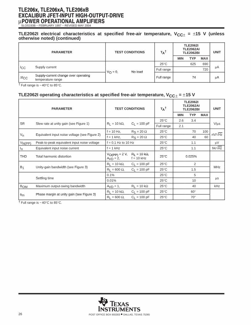
ICC Supply current25°C 625 690
AICC Supply currentVO = 0, No load
Full range 720µA
∆ICCSupply-current change over operating
VO = 0, No load
Full range 74 µA∆ICCSupply-current change over operatingtemperature range
Full range 74 µA
† Full range is −40°C to 85°C.
TLE2062I operating characteristics at specified free-air temperature, V CC± = ±15 V
PARAMETER TEST CONDITIONS TA†
TLE2062ITLE2062AITLE2062BI UNITA
MIN TYP MAX
SR Slew rate at unity gain (see Figure 1) RL = 10 kΩ, CL = 100 pF25°C 2.6 3.4
V/ sSR Slew rate at unity gain (see Figure 1) RL = 10 kΩ, CL = 100 pFFull range 2.1
V/µs
Vn Equivalent input noise voltage (see Figure 2)f = 10 Hz, RS = 20 Ω 25°C 70 100
nV/√HzVn Equivalent input noise voltage (see Figure 2)f = 1 kHz, RS = 20 Ω 25°C 40 60
nV/√Hz
VN(PP) Peak-to-peak equivalent input noise voltage f = 0.1 Hz to 10 Hz 25°C 1.1 µV
In Equivalent input noise current f = 1 kHz 25°C 1.1 fA/√Hz
THD Total harmonic distortionVO(PP) = 2 V, RL = 10 kΩ,
25°C 0.025%THD Total harmonic distortionVO(PP) = 2 V,AVD = 2,
RL = 10 kΩ,f = 10 kHz 25°C 0.025%
B1 Unity-gain bandwidth (see Figure 3)RL = 10 kΩ, CL = 100 pF 25°C 2
MHzB1 Unity-gain bandwidth (see Figure 3)RL = 600 Ω, CL = 100 pF 25°C 1.5
MHz
Settling time0.1% 25°C 5
sSettling time0.01% 25°C 10
µs
BOM Maximum output-swing bandwidth AVD = 1, RL = 10 kΩ 25°C 40 kHz
φm Phase margin at unity gain (see Figure 3)RL = 10 kΩ, CL = 100 pF 25°C 60°
φm Phase margin at unity gain (see Figure 3)RL = 600 Ω, CL = 100 pF 25°C 70°
† Full range is −40°C to 85°C.

µ
SLOS193B − FEBRUARY 1997 − REVISED MAY 2004
27POST OFFICE BOX 655303 • DALLAS, TEXAS 75265
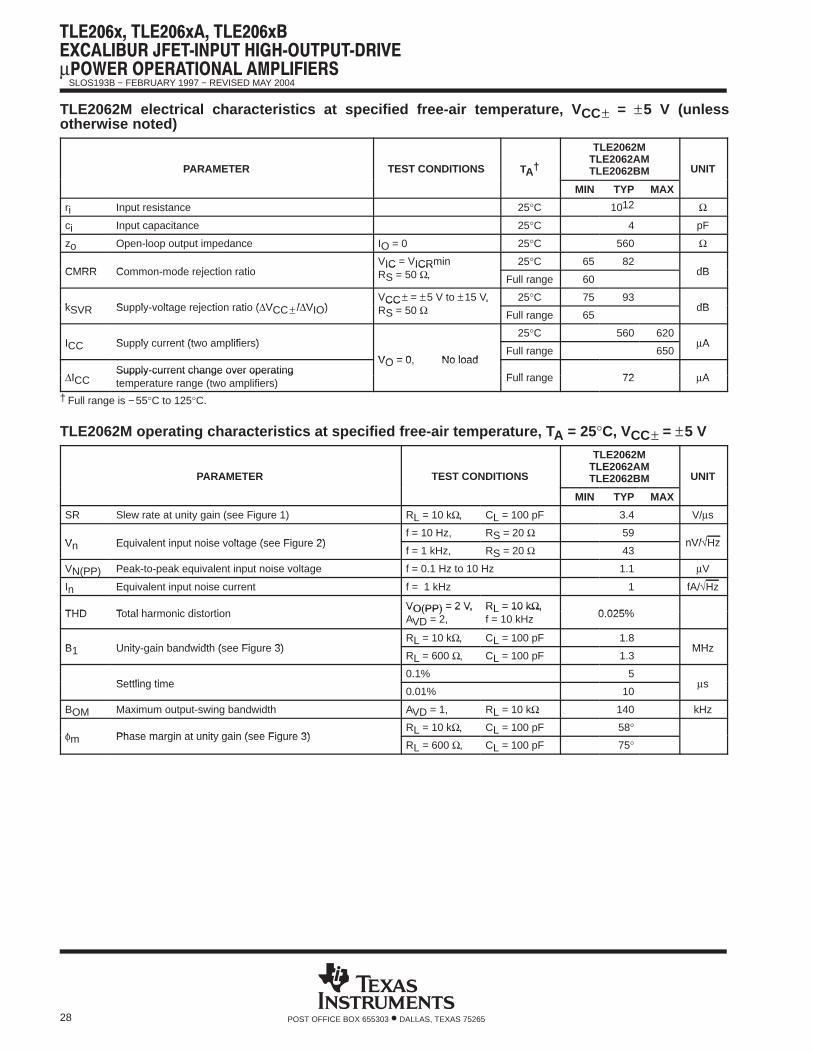
TLE2062M electrical characteristics at specified free-air temperature, V CC± = ±5 V
PARAMETER TEST CONDITIONS TA†
TLE2062MTLE2062AMTLE2062BM UNITA
MIN TYP MAX
TLE2062M25°C 1 5
TLE2062MFull range 7
VIO Input offset voltage TLE2062AM25°C 0.9 4
mVVIO Input offset voltage TLE2062AMFull range 6
mV
TLE2062BM25°C 0.7 3
TLE2062BM
VIC = 0, RS = 50 ΩFull range 5
αVIO Temperature coefficient of input offset voltageVIC = 0, RS = 50 Ω
Full range 6 µV/°C
Input offset voltage long-term drift (see Note 4) 25°C 0.04 µV/mo
IIO Input offset current25°C 1 pA
IIO Input offset currentFull range 15 nA
IIB Input bias current25°C 3 pA
IIB Input bias currentFull range 30 nA
VICR Common-mode input voltage range
25°C−1.6
to4
−2to6
V
VICR Common-mode input voltage range
Full range−1.6
to4
V
RL = 10 kΩ25°C 3.5 3.7
RL = 10 kΩFull range 3
VOM+Maximum positive peak output FK and JG
packages RL = 600 Ω25°C 2.5 3.6
VVOM+Maximum positive peak outputvoltage swing
FK and JGpackages RL = 600 Ω
Full range 2Vvoltage swing
D and Ppackages RL = 100 Ω
25°C 2.5 3.1D and Ppackages RL = 100 Ω
Full range 2
RL = 10 kΩ25°C −3.5 −3.9
RL = 10 kΩFull range −3
VOM−Maximum negative peak output FK and JG
packages RL = 600 Ω25°C −2.5 −3.5
VVOM−Maximum negative peak outputvoltage swing
FK and JGpackages RL = 600 Ω
Full range −2Vvoltage swing
D and Ppackages RL = 100 Ω
25°C −2.5 −2.7D and Ppackages RL = 100 Ω
Full range −2
VO = ±2.8 V, RL = 10 kΩ25°C 15 80
VO = ±2.8 V, RL = 10 kΩFull range 2
VO = 0 to 2.5 V, RL = 600 Ω25°C 1 65
FK and JGpackages
VO = 0 to 2.5 V, RL = 600 ΩFull range 0.5
AVDLarge-signal differential voltage
FK and JGpackages
VO = 0 to −2.5 V, RL = 600 Ω25°C 1 16
V/mVAVDLarge-signal differential voltageamplification VO = 0 to −2.5 V, RL = 600 Ω
Full range 0.5V/mVamplification
VO = 0 to 2 V, RL = 100 Ω25°C 0.75 45
D and Ppackages
VO = 0 to 2 V, RL = 100 ΩFull range 0.5D and P
packagesVO = 0 to −2 V, RL = 100 Ω
25°C 0.5 3VO = 0 to −2 V, RL = 100 Ω
Full range 0.25† Full range is −55°C to 125°C.NOTE 4: Typical values are based on the input offset voltage shift observed through 168 hours of operating life test at TA = 150°C extrapolated
to TA = 25 °C using the Arrhenius equation and assuming an activation energy of 0.96 eV.
µ
SLOS193B − FEBRUARY 1997 − REVISED MAY 2004
28 POST OFFICE BOX 655303 • DALLAS, TEXAS 75265
TLE2062M electrical characteristics at specified free-air temperature, V CC± = ±5 V (unlessotherwise noted)
PARAMETER TEST CONDITIONS TA†
TLE2062MTLE2062AMTLE2062BM UNITA
MIN TYP MAX
ri Input resistance 25°C 1012 Ω
ci Input capacitance 25°C 4 pF
zo Open-loop output impedance IO = 0 25°C 560 Ω
CMRR Common-mode rejection ratioVIC = VICRminR = 50 ,
25°C 65 82dBCMRR Common-mode rejection ratio
VIC = VICRminRS = 50 Ω, Full range 60
dB
kSVR Supply-voltage rejection ratio (∆VCC /∆VIO)VCC± = ±5 V to ±15 V,R = 50
25°C 75 93dBkSVR Supply-voltage rejection ratio (∆VCC± /∆VIO)
VCC = 5 V to 15 V,RS = 50 Ω Full range 65
dB
ICC Supply current (two amplifiers)25°C 560 620
AICC Supply current (two amplifiers)
VO = 0, No loadFull range 650
µA
∆ICCSupply-current change over operating
VO = 0, No load
Full range 72 A∆ICCSupply-current change over operatingtemperature range (two amplifiers) Full range 72 µA
† Full range is −55°C to 125°C.
TLE2062M operating characteristics at specified free-air temperature, T A = 25°C, VCC± = ±5 V
PARAMETER TEST CONDITIONS
TLE2062MTLE2062AMTLE2062BM UNIT
MIN TYP MAX
SR Slew rate at unity gain (see Figure 1) RL = 10 kΩ, CL = 100 pF 3.4 V/µs
Vn Equivalent input noise voltage (see Figure 2)f = 10 Hz, RS = 20 Ω 59
nV/√HzVn Equivalent input noise voltage (see Figure 2)f = 1 kHz, RS = 20 Ω 43
nV/√Hz
VN(PP) Peak-to-peak equivalent input noise voltage f = 0.1 Hz to 10 Hz 1.1 µV
In Equivalent input noise current f = 1 kHz 1 fA/√Hz
THD Total harmonic distortionVO(PP) = 2 V, RL = 10 kΩ,
0.025%THD Total harmonic distortionVO(PP) = 2 V,AVD = 2,
RL = 10 kΩ,f = 10 kHz 0.025%
B1 Unity-gain bandwidth (see Figure 3)RL = 10 kΩ, CL = 100 pF 1.8
MHzB1 Unity-gain bandwidth (see Figure 3)RL = 600 Ω, CL = 100 pF 1.3
MHz
Settling time0.1% 5
sSettling time0.01% 10
µs
BOM Maximum output-swing bandwidth AVD = 1, RL = 10 kΩ 140 kHz
φm Phase margin at unity gain (see Figure 3)RL = 10 kΩ, CL = 100 pF 58°
φm Phase margin at unity gain (see Figure 3)RL = 600 Ω, CL = 100 pF 75°

µ
SLOS193B − FEBRUARY 1997 − REVISED MAY 2004
29POST OFFICE BOX 655303 • DALLAS, TEXAS 75265
TLE2062M electrical characteristics at specified free-air temperature, V CC± = ±15 V (unlessotherwise noted)
PARAMETER TEST CONDITIONS TA†
TLE2062MTLE2062AMTLE2062BM UNITA
MIN TYP MAX
TLE2062M25°C 0.9 4
TLE2062MFull range 6
VIO Input offset voltage TLE2062AM25°C 0.8 2
mVVIO Input offset voltage TLE2062AMFull range 4
mV
TLE2062BM25°C 0.5 1
TLE2062BM
VIC = 0, RS = 50 ΩFull range 3
αVIO Temperature coefficient of input offset voltageVIC = 0, RS = 50 Ω
Full range 6 µV/°C
Input offset voltage long-term drift (see Note 4) 25°C 0.04 µV/mo
IIO Input offset current25°C 2 pA
IIO Input offset currentFull range 20 nA
IIB Input bias current25°C 4 pA
IIB Input bias currentFull range 40 nA
VICR Common-mode input voltage range
25°C−11
to13
−12to16
V
VICR Common-mode input voltage range
Full range−11
to13
V
RL = 10 kΩ25°C 13 13.7
VOM+ Maximum positive peak output voltage swing
RL = 10 kΩFull range 12.5
VVOM+ Maximum positive peak output voltage swing
RL = 600 Ω25°C 12.5 13.2
V
RL = 600 ΩFull range 11
RL = 10 kΩ25°C −13 −13.7
VOM− Maximum negative peak output voltage swing
RL = 10 kΩFull range −12.5
VVOM− Maximum negative peak output voltage swing
RL = 600 Ω25°C −12.5 −13
V
RL = 600 ΩFull range −11
VO = ± 10 V, RL = 10 kΩ25°C 30 230
VO = ± 10 V, RL = 10 kΩFull range 20
AVD Large-signal differential voltage amplification VO = 0 to 8 V, RL = 600 Ω25°C 25 100
V/mVAVD Large-signal differential voltage amplification VO = 0 to 8 V, RL = 600 ΩFull range 7
V/mV
VO = 0 to −8 V, RL = 600 Ω25°C 3 25
VO = 0 to −8 V, RL = 600 ΩFull range 1
ri Input resistance 25°C 1012 Ω
ci Input capacitance 25°C 4 pF
zo Open-loop output impedance IO = 0 25°C 560 Ω
CMRR Common-mode rejection ratio VIC = VICRmin, RS = 50 Ω25°C 72 90
dBCMRR Common-mode rejection ratio VIC = VICRmin, RS = 50 ΩFull range 65
dB
kSVR Supply-voltage rejection ratio (∆VCC /∆VIO)VCC± = ± 5 V to ± 15 V, 25°C 75 93
dBkSVR Supply-voltage rejection ratio (∆VCC± /∆VIO)VCC± = ± 5 V to ± 15 V,RS = 50 Ω Full range 65
dB
† Full range is −55°C to 125°C.NOTE 4: Typical values are based on the input offset voltage shift observed through 168 hours of operating life test at TA = 150°C extrapolated
to TA = 25 °C using the Arrhenius equation and assuming an activation energy of 0.96 eV.

µ
SLOS193B − FEBRUARY 1997 − REVISED MAY 2004
30 POST OFFICE BOX 655303 • DALLAS, TEXAS 75265
TLE2062M electrical characteristics at specified free-air temperature, V CC± = ±15 V (unlessotherwise noted)
PARAMETER TEST CONDITIONS TA†
TLE2062MTLE2062AMTLE2062BM UNITA
MIN TYP MAX
ICC Supply current25°C 625 690
AICC Supply currentVO = 0, No load
Full range 730µA
∆ICCSupply-current change over operating
VO = 0, No load
Full range 97 µA∆ICCSupply-current change over operatingtemperature range
Full range 97 µA
† Full range is −55°C to 125°C.
TLE2062M operating characteristics at specified free-air temperature, V CC± = ±15 V
PARAMETER TEST CONDITIONS TA†
TLE2062MTLE2062AMTLE2062BM UNITA
MIN TYP MAX
SR Slew rate at unity gain (see Figure 1) RL = 10 kΩ, CL = 100 pF25°C 2 3.4
V/ sSR Slew rate at unity gain (see Figure 1) RL = 10 kΩ, CL = 100 pFFull range 1.8
V/µs
Vn Equivalent input noise voltage (see Figure 2)f = 10 Hz, RS = 20 Ω 25°C 70
nV/√HzVn Equivalent input noise voltage (see Figure 2)f = 1 kHz, RS = 20 Ω 25°C 40
nV/√Hz
VN(PP) Peak-to-peak equivalent input noise voltage f = 0.1 Hz to 10 Hz 25°C 1.1 µV
In Equivalent input noise current f = 1 kHz 25°C 1.1 fA/√Hz
THD Total harmonic distortionVO(PP) = 2 V,AVD = 2,
RL = 10 kΩ,f = 10 kHz
25°C 0.025%
B1 Unity-gain bandwidth (see Figure 3)RL = 10 kΩ, CL = 100 pF 25°C 2
MHzB1 Unity-gain bandwidth (see Figure 3)RL = 600 Ω, CL = 100 pF 25°C 1.5
MHz
Settling time0.1% 25°C 5
sSettling time0.01% 25°C 10
µs
BOM Maximum output-swing bandwidth AVD = 1, RL = 10 kΩ 25°C 40 kHzBOM Maximum output-swing bandwidth AVD = 1, RL = 10 kΩ 25°C 40 kHz
φm Phase margin at unity gain (see Figure 3)RL = 10 kΩ, CL = 100 pF 25°C 60°
φm Phase margin at unity gain (see Figure 3)RL = 600 Ω, CL = 100 pF 25°C 70°
† Full range is −55°C to 125°C.

µ
SLOS193B − FEBRUARY 1997 − REVISED MAY 2004
31POST OFFICE BOX 655303 • DALLAS, TEXAS 75265
TLE2062Y electrical characteristics at V CC± = ±15 V, TA = 25°C (unless otherwise noted)
PARAMETER TEST CONDITIONSTLE2062Y
UNITPARAMETER TEST CONDITIONSMIN TYP MAX
UNIT
VIO Input offset voltage 0.9 4 mV
αVIO Input offset voltage long-term drift (see Note 4)VIC = 0, RS = 50 Ω
0.04 µV/mo
IIO Input offset currentVIC = 0, RS = 50 Ω
2 pA
IIB Input bias current 4 pA
−11 −12VICR Common-mode input voltage range
−11to
−12to VVICR Common-mode input voltage range to
13to16
V
VOM+ Maximum positive peak output voltage swingRL = 10 kΩ 13.2 13.7
VVOM+ Maximum positive peak output voltage swingRL = 600 Ω 12.5 13.2
V
VOM− Maximum negative peak output voltage swingRL = 10 kΩ −13.2 −13.7
VVOM− Maximum negative peak output voltage swingRL = 600 Ω −12.5 −13
V
VO = ±10 V, RL = 10 kΩ 30 230
AVD Large-signal differential voltage amplification VO = 0 to 8 V, RL = 600 Ω 25 100 V/mVAVD Large-signal differential voltage amplification
VO = 0 to −8 V, RL = 600 Ω 3 25
V/mV
ri Input resistance 1012 Ω
ci Input capacitance 4 pF
zo Open-loop output impedance IO = 0 560 Ω
CMRR Common-mode rejection ratio VIC = VICRmin, RS = 50 Ω 72 90 dB
kSVR Supply-voltage rejection ratio (∆VCC/∆VIO)VCC± = ±5 V to ±15 V,
75 93 dBkSVR Supply-voltage rejection ratio (∆VCC/∆VIO)VCC± = ±5 V to ±15 V,RS = 50 Ω 75 93 dB
ICC Supply current VO = 0, No load 625 690 µA
NOTE 4: Typical values are based on the input offset voltage shift observed through 168 hours of operating life test at TA = 150°C extrapolatedto TA = 25 °C using the Arrhenius equation and assuming an activation energy of 0.96 eV.
TLE2062Y operating characteristics at V CC± = ±15 V, TA = 25°C
PARAMETER TEST CONDITIONSTLE2062Y
UNITPARAMETER TEST CONDITIONSMIN TYP MAX
UNIT
SR Slew rate at unity gain (see Figure 1) RL = 10 kΩ, CL = 100 pF 2.6 3.4 4 V/µs
Vn Equivalent input noise voltage (see Figure 2)f = 10 Hz, RS = 20 Ω 70
nV/√HzVn Equivalent input noise voltage (see Figure 2)f = 1 kHz, RS = 20 Ω 40
nV/√Hz
VN(PP) Peak-to-peak equivalent input noise voltage f = 0.1 Hz to 10 Hz 1.1 µV
In Equivalent input noise current f = 1 Hz 1.1 fA/√Hz
THD Total harmonic distortionVO(PP) = 2 V,AVD = 2,
RL = 10 kΩ,f = 10 kHz
0.025%
B1 Unity-gain bandwidth (see Figure 3)RL = 10 kΩ, CL = 100 pF 2
MHzB1 Unity-gain bandwidth (see Figure 3)RL = 600 Ω, CL = 100 pF 1.5
MHz
Settling time0.1% 5
sSettling time0.01% 10
µs
BOM Maximum output-swing bandwidth AVD = 1, RL = 10 kΩ 40 kHz
φm Phase margin at unity gain (see Figure 3)RL = 10 kΩ, CL = 100 pF 60°
φm Phase margin at unity gain (see Figure 3)RL = 600 Ω, CL = 100 pF 70°

µ
SLOS193B − FEBRUARY 1997 − REVISED MAY 2004
32 POST OFFICE BOX 655303 • DALLAS, TEXAS 75265
TLE2064C electrical characteristics at specified free-air temperature, V CC± = ±5 V (unlessotherwise noted)
PARAMETER TEST CONDITIONS TA†
TLE2064CTLE2064ACTLE2064BC UNITA
MIN TYP MAX
TLE2064C25°C 1.2 7
TLE2064CFull range 7.9
VIO Input offset voltage TLE2064AC25°C 1.2 6
mVVIO Input offset voltage TLE2064ACFull range 6.9
mV
TLE2064BC25°C 0.8 3.5
TLE2064BC
VIC = 0, RS = 50 ΩFull range 4.4
αVIO Temperature coefficient of input offset voltageVIC = 0, RS = 50 Ω
25°C 6 µV/°CInput offset voltage long-term drift (see Note 4) Full range 0.04 µV/mo
IIO Input offset current25°C 1 pA
IIO Input offset currentFull range 0.8 nA
IIB Input bias current25°C 3 pA
IIB Input bias currentFull range 2 nA
VICR Common-mode input voltage range
25°C−1.6
to4
−2to6
V
VICR Common-mode input voltage range
Full range−1.6
to4
V
RL = 10 kΩ25°C 3.5 3.7
VOM+ Maximum positive peak output voltage swing
RL = 10 kΩFull range 3.3
VVOM+ Maximum positive peak output voltage swing
RL = 100 Ω25°C 2.5 3.1
V
RL = 100 ΩFull range 2
RL = 10 kΩ25°C −3.7 −3.9
VOM− Maximum negative peak output voltage swing
RL = 10 kΩFull range −3.3
VVOM− Maximum negative peak output voltage swing
RL = 100 Ω25°C −2.5 −2.7
V
RL = 100 ΩFull range −2
VO = ±2.8 V, RL = 10 kΩ25°C 15 80
VO = ±2.8 V, RL = 10 kΩFull range 2
AVD Large-signal differential voltage amplification VO = 0 to 2 V, RL = 100 Ω25°C 0.75 45
V/mVAVD Large-signal differential voltage amplification VO = 0 to 2 V, RL = 100 ΩFull range 0.5
V/mV
VO = 0 to −2 V, RL = 100 Ω25°C 0.5 3
VO = 0 to −2 V, RL = 100 ΩFull range 0.15
ri Input resistance 25°C 1012 Ωci Input capacitance 25°C 4 pF
zo Open-loop output impedance IO = 0 25°C 560 Ω
CMRR Common-mode rejection ratio VIC = VICRmin, RS = 50 Ω25°C 65 82
dBCMRR Common-mode rejection ratio VIC = VICRmin, RS = 50 ΩFull range 65
dB
kSVR Supply-voltage rejection ratio (∆VCC /∆VIO)VCC± = ±5 V to ±15 V, 25°C 75 93
dBkSVR Supply-voltage rejection ratio (∆VCC± /∆VIO)VCC± = ±5 V to ±15 V,RS = 50 Ω Full range 75
dB
† Full range is 0°C to 70°C.NOTE 4: Typical values are based on the input offset voltage shift observed through 168 hours of operating life test at TA = 150°C extrapolated
to TA = 25°C using the Arrhenius equation and assuming an activation energy of 0.96 eV.

µ
SLOS193B − FEBRUARY 1997 − REVISED MAY 2004
33POST OFFICE BOX 655303 • DALLAS, TEXAS 75265
TLE2064C electrical characteristics at specified free-air temperature, V CC± = ±5 V (unlessotherwise noted) (continued)
PARAMETER TEST CONDITIONS TA†
TLE2064CTLE2064ACTLE2064BC UNITA
MIN TYP MAX
ICC Supply current (four amplifiers)25°C 1.12 1.3
mAICC Supply current (four amplifiers)
VO = 0, No loadFull range 1.3
mA
∆ICCSupply-current change over operating
VO = 0, No load
Full range 52 A∆ICCSupply-current change over operatingtemperature range (four amplifiers) Full range 52 µA
VO1/VO2 Crosstalk attenuation AVD = 1000, f = 1 kHz 25°C 120 dB
† Full range is 0°C to 70°C.
TLE2064C operating characteristics at specified free-air temperature, V CC± = ±5 V
PARAMETER TEST CONDITIONS TA†
TLE2064CTLE2064ACTLE2064BC UNITA
MIN TYP MAX
SR Slew rate at unity gain (see Figure 1) RL = 10 kΩ, CL = 100 pF25°C 2.2 3.4
V/ sSR Slew rate at unity gain (see Figure 1) RL = 10 kΩ, CL = 100 pFFull range 2.1
V/µs
Vn Equivalent input noise voltage (see Figure 2)f = 10 Hz, RS = 20 Ω
25°C59 100
nV/√HzVn Equivalent input noise voltage (see Figure 2)f = 1 kHz , RS = 20 Ω
25°C43 60
nV/√Hz
VN(PP) Peak-to-peak equivalent input noise voltage f = 0.1 Hz to 10 Hz 25°C 1.1 µV
In Equivalent input noise current f = 1 kHz 25°C 1 fA/√Hz
THD Total harmonic distortionAVD = 2, f = 10 kHz,
25°C 0.025%THD Total harmonic distortionAVD = 2,VO(PP) = 2 V,
f = 10 kHz,RL = 10 kΩ 25°C 0.025%
B1 Unity-gain bandwidth (see Figure 3)RL = 10 kΩ, CL = 100 pF
25°C1.8
MHzB1 Unity-gain bandwidth (see Figure 3)RL = 100 Ω, CL = 100 pF
25°C1.3
MHz
ts Settling timeε = 0.1%
25°C5
sts Settling timeε = 0.01%
25°C10
µs
BOM Maximum output-swing bandwidth AVD = 1, RL = 10 kΩ 25°C 140 kHz
φm Phase margin at unity gain (see Figure 3)RL = 10 kΩ, CL = 100 pF
25°C58°
φm Phase margin at unity gain (see Figure 3)RL = 100 Ω, CL = 100 pF
25°C75°
† Full range is 0°C to 70°C.

µ
SLOS193B − FEBRUARY 1997 − REVISED MAY 2004
34 POST OFFICE BOX 655303 • DALLAS, TEXAS 75265
TLE2064C electrical characteristics at specified free-air temperature, V CC± = ±15 V (unlessotherwise noted)
PARAMETER TEST CONDITIONS TA†
TLE2064CTLE2064ACTLE2064BC UNITA
MIN TYP MAX
TLE2064C25°C 0.9 6
TLE2064CFull range 6.9
VIO Input offset voltage TLE2064AC25°C 0.9 4
mVVIO Input offset voltage TLE2064ACFull range 4.9
mV
TLE2064BC25°C 0.7 2
TLE2064BC
VIC = 0, RS = 50 ΩFull range 4
αVIO Temperature coefficient of input offset voltageVIC = 0, RS = 50 Ω
25°C 6 µV/°C
Input offset voltage long-term drift (see Note 4) Full range 0.04 µV/mo
IIO Input offset current25°C 2 pA
IIO Input offset currentFull range 1 nA
IIB Input bias current25°C 4 pA
IIB Input bias currentFull range 3 nA
VICR Common-mode input voltage range
25°C−11
to13
−12to16
V
VICR Common-mode input voltage range
Full range−11
to13
V
RL = 10 kΩ25°C 13.2 13.7
VOM+ Maximum positive peak output voltage swing
RL = 10 kΩFull range 13
VVOM+ Maximum positive peak output voltage swing
RL = 600 Ω25°C 12.5 13.2
V
RL = 600 ΩFull range 12
RL = 10 kΩ25°C −13.2 −13.7
VOM− Maximum negative peak output voltage swing
RL = 10 kΩFull range −13
VVOM− Maximum negative peak output voltage swing
RL = 600 Ω25°C −12.5 −13
V
RL = 600 ΩFull range −12
VO = ±10 V, RL = 10 kΩ25°C 30 230
VO = ±10 V, RL = 10 kΩFull range 20
AVD Large-signal differential voltage amplification VO = 0 to 8 V, RL = 600 Ω25°C 25 100
V/mVAVD Large-signal differential voltage amplification VO = 0 to 8 V, RL = 600 ΩFull range 10
V/mV
VO = 0 to −8 V, RL = 600 Ω25°C 3 25
VO = 0 to −8 V, RL = 600 ΩFull range 1
ri Input resistance 25°C 1012 Ω
ci Input capacitance 25°C 4 pF
zo Open-loop output impedance IO = 0 25°C 560 Ω
CMRR Common-mode rejection ratio VIC = VICRmin, RS = 50 Ω25°C 72 90
dBCMRR Common-mode rejection ratio VIC = VICRmin, RS = 50 ΩFull range 70
dB
kSVR Supply-voltage rejection ratio (∆VCC /∆VIO)VCC± = ±5 V to ±15 V, 25°C 75 93
dBkSVR Supply-voltage rejection ratio (∆VCC± /∆VIO)VCC± = ±5 V to ±15 V,RS = 50 Ω Full range 75
dB
† Full range is 0°C to 70°C.NOTE 4: Typical values are based on the input offset voltage shift observed through 168 hours of operating life test at TA = 150°C extrapolated
to TA = 25°C using the Arrhenius equation and assuming an activation energy of 0.96 eV.

µ
SLOS193B − FEBRUARY 1997 − REVISED MAY 2004
35POST OFFICE BOX 655303 • DALLAS, TEXAS 75265
TLE2064C electrical characteristics at specified free-air temperature, V CC± = ±15 V (unlessotherwise noted) (continued)
PARAMETER TEST CONDITIONS TA†
TLE2064CTLE2064ACTLE2064BC UNITA
MIN TYP MAX
ICC Supply current (four amplifiers)25°C 1.25 1.4
mAICC Supply current (four amplifiers)VO = 0, No load
Full range 1.5mA
∆ICCSupply-current change over operating
VO = 0, No load
Full range 72 µA∆ICCSupply-current change over operating temperature range (four amplifiers)
Full range 72 µA
VO1/VO2 Crosstalk attenuation AVD = 1000, f = 1 kHz 25°C 120 dB
† Full range is 0°C to 70°C.
TLE2064C operating characteristics at specified free-air temperature, V CC± = ±15 V
PARAMETER TEST CONDITIONS TA†
TLE2064CTLE2064ACTLE2064BC UNITA
MIN TYP MAX
SR Slew rate at unity gain (see Figure 1) RL = 10 kΩ, CL = 100 pF25°C 2.6 3.4
V/ sSR Slew rate at unity gain (see Figure 1) RL = 10 kΩ, CL = 100 pFFull range 2.5
V/µs
Vn Equivalent input noise voltage (see Figure 2)f = 10 Hz, RS = 20 Ω
25°C70 100
nV/√HzVn Equivalent input noise voltage (see Figure 2)f = 1 kHz , RS = 20 Ω
25°C40 60
nV/√Hz
VN(PP) Peak-to-peak equivalent input noise voltage f = 0.1 Hz to 10 Hz 25°C 1.1 µV
In Equivalent input noise current f = 1 kHz 25°C 1 fA/√Hz
THD Total harmonic distortionAVD = 2, f = 10 kHz,
25°C 0.025%THD Total harmonic distortionAVD = 2,VO(PP) = 2 V,
f = 10 kHz,RL = 10 kΩ 25°C 0.025%
B1 Unity-gain bandwidth (see Figure 3)RL = 10 kΩ, CL = 100 pF
25°C2
MHzB1 Unity-gain bandwidth (see Figure 3)RL = 600 Ω, CL = 100 pF
25°C1.5
MHz
ts Settling timeε = 0.1%
25°C5
sts Settling timeε = 0.01%
25°C10
µs
BOM Maximum output-swing bandwidth AVD = 1, RL = 10 kΩ 25°C 40 kHz
φm Phase margin at unity gain (see Figure 3)RL = 10 kΩ, CL = 100 pF
25°C50°
φm Phase margin at unity gain (see Figure 3)RL = 600 Ω, CL = 100 pF
25°C70°
† Full range is 0°C to 70°C.
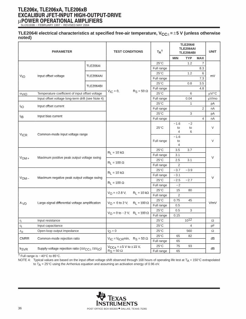
µ
SLOS193B − FEBRUARY 1997 − REVISED MAY 2004
36 POST OFFICE BOX 655303 • DALLAS, TEXAS 75265
TLE2064I electrical characteristics at specified free-air temperature, V CC± = ±5 V (unless otherwisenoted)
PARAMETER TEST CONDITIONS TA†
TLE2064ITLE2064AITLE2064BI UNITA
MIN TYP MAX
TLE2064I25°C 1.2 7
TLE2064IFull range 8.3
VIO Input offset voltage TLE2064AI25°C 1.2 6
mVVIO Input offset voltage TLE2064AIFull range 7.3
mV
TLE2064BI25°C 0.8 3.5
TLE2064BI
VIC = 0, RS = 50 ΩFull range 4.8
αVIO Temperature coefficient of input offset voltageVIC = 0, RS = 50 Ω
25°C 6 µV/°CInput offset voltage long-term drift (see Note 4) Full range 0.04 µV/mo
IIO Input offset current25°C 1 pA
IIO Input offset currentFull range 2 nA
IIB Input bias current25°C 3 pA
IIB Input bias currentFull range 4 nA
VICR Common-mode input voltage range
25°C−1.6
to4
−2to6
V
VICR Common-mode input voltage range
Full range−1.6
to4
V
RL = 10 kΩ25°C 3.5 3.7
VOM+ Maximum positive peak output voltage swing
RL = 10 kΩFull range 3.1
VVOM+ Maximum positive peak output voltage swing
RL = 100 Ω25°C 2.5 3.1
V
RL = 100 ΩFull range 2
RL = 10 kΩ25°C −3.7 −3.9
VOM− Maximum negative peak output voltage swing
RL = 10 kΩFull range −3.1
VVOM− Maximum negative peak output voltage swing
RL = 100 Ω25°C −2.5 −2.7
V
RL = 100 ΩFull range −2
VO = ±2.8 V, RL = 10 kΩ25°C 15 80
VO = ±2.8 V, RL = 10 kΩFull range 2
AVD Large-signal differential voltage amplification VO = 0 to 2 V, RL = 100 Ω25°C 0.75 45
V/mVAVD Large-signal differential voltage amplification VO = 0 to 2 V, RL = 100 ΩFull range 0.5
V/mV
VO = 0 to −2 V, RL = 100 Ω25°C 0.5 3
VO = 0 to −2 V, RL = 100 ΩFull range 0.15
ri Input resistance 25°C 1012 Ωci Input capacitance 25°C 4 pF
zo Open-loop output impedance IO = 0 25°C 560 Ω
CMRR Common-mode rejection ratio VIC = VICRmin, RS = 50 Ω25°C 65 82
dBCMRR Common-mode rejection ratio VIC = VICRmin, RS = 50 ΩFull range 65
dB
kSVR Supply-voltage rejection ratio (∆VCC /∆VIO)VCC± = ±5 V to ±15 V, 25°C 75 93
dBkSVR Supply-voltage rejection ratio (∆VCC± /∆VIO)VCC± = ±5 V to ±15 V,RS = 50 Ω Full range 65
dB
† Full range is −40°C to 85°C.NOTE 4: Typical values are based on the input offset voltage shift observed through 168 hours of operating life test at TA = 150°C extrapolated
to TA = 25°C using the Arrhenius equation and assuming an activation energy of 0.96 eV.

µ
SLOS193B − FEBRUARY 1997 − REVISED MAY 2004
37POST OFFICE BOX 655303 • DALLAS, TEXAS 75265
TLE2064I electrical characteristics at specified free-air temperature, V CC± = ±5 V (unless otherwisenoted) (continued)
PARAMETER TEST CONDITIONS TA†
TLE2064ITLE2064AITLE2064BI UNITA
MIN TYP MAX
ICC Supply current (four amplifiers)25°C 1.12 1.3
mAICC Supply current (four amplifiers)VO = 0, No load
Full range 1.3mA
∆ICCSupply-current change over operating
VO = 0, No load
Full range 108 µA∆ICCSupply-current change over operating temperature range (four amplifiers)
Full range 108 µA
VO1/VO2 Crosstalk attenuation AVD = 1000, f = 1 kHz 25°C 120 dB
† Full range is −40°C to 85°C.
TLE2064I operating characteristics at specified free-air temperature, V CC± = ±5 V (unless otherwisenoted)
PARAMETER TEST CONDITIONS TA†
TLE2064ITLE2064AITLE2064BI UNITA
MIN TYP MAX
SR Slew rate at unity gain (see Figure 1) RL = 10 kΩ, CL = 100 pF25°C 2.2 3.4
V/ sSR Slew rate at unity gain (see Figure 1) RL = 10 kΩ, CL = 100 pFFull range 1.7
V/µs
Vn Equivalent input noise voltage (see Figure 2)f = 10 Hz, RS = 20 Ω
25°C59 100
nV/√HzVn Equivalent input noise voltage (see Figure 2)f = 1 kHz , f = 1 kHz ,
25°C43 60
nV/√Hz
VN(PP) Peak-to-peak equivalent input noise voltage f = 0.1 Hz to 10 Hz 25°C 1.1 µV
In Equivalent input noise current f = 1 kHz 25°C 1 fA/√Hz
THD Total harmonic distortionAVD = 2,VO(PP) = 2 V,
f = 10 kHz,RL = 10 kΩ 25°C 0.025%
B1 Unity-gain bandwidth (see Figure 3)RL = 10 kΩ, CL = 100 pF
25°C1.8
MHzB1 Unity-gain bandwidth (see Figure 3)RL = 100 Ω, CL = 100 pF
25°C1.3
MHz
ts Settling timeε = 0.1%
25°C5
sts Settling timeε = 0.01%
25°C10
µs
BOM Maximum output-swing bandwidth AVD = 1, RL = 10 kΩ 25°C 140 kHz
φm Phase margin at unity gain (see Figure 3)RL = 10 kΩ, CL = 100 pF
25°C58°
φm Phase margin at unity gain (see Figure 3)RL = 100 Ω, CL = 100 pF
25°C75°
† Full range is − 40°C to 85°C.
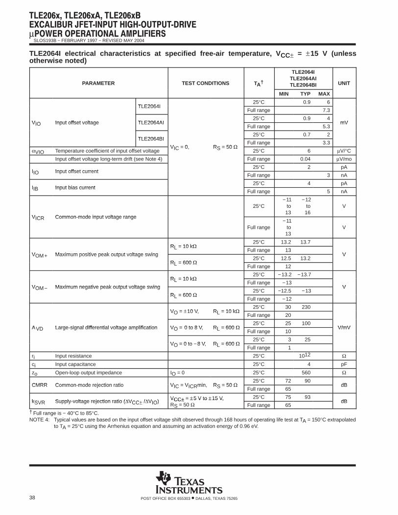
µ
SLOS193B − FEBRUARY 1997 − REVISED MAY 2004
38 POST OFFICE BOX 655303 • DALLAS, TEXAS 75265
TLE2064I electrical characteristics at specified free-air temperature, V CC± = ±15 V (unlessotherwise noted)
PARAMETER TEST CONDITIONS TA†
TLE2064ITLE2064AITLE2064BI UNITA
MIN TYP MAX
TLE2064I25°C 0.9 6
TLE2064IFull range 7.3
VIO Input offset voltage TLE2064AI25°C 0.9 4
mVVIO Input offset voltage TLE2064AIFull range 5.3
mV
TLE2064BI25°C 0.7 2
TLE2064BI
VIC = 0, RS = 50 ΩFull range 3.3
αVIO Temperature coefficient of input offset voltageVIC = 0, RS = 50 Ω
25°C 6 µV/°CInput offset voltage long-term drift (see Note 4) Full range 0.04 µV/mo
IIO Input offset current25°C 2 pA
IIO Input offset currentFull range 3 nA
IIB Input bias current25°C 4 pA
IIB Input bias currentFull range 5 nA
VICR Common-mode input voltage range
25°C−11
to13
−12to16
V
VICR Common-mode input voltage range
Full range−11
to13
V
RL = 10 kΩ25°C 13.2 13.7
VOM+ Maximum positive peak output voltage swing
RL = 10 kΩFull range 13
VVOM+ Maximum positive peak output voltage swing
RL = 600 Ω25°C 12.5 13.2
V
RL = 600 ΩFull range 12
RL = 10 kΩ25°C −13.2 −13.7
VOM− Maximum negative peak output voltage swing
RL = 10 kΩFull range −13
VVOM− Maximum negative peak output voltage swing
RL = 600 Ω25°C −12.5 −13
V
RL = 600 ΩFull range −12
VO = ±10 V, RL = 10 kΩ25°C 30 230
VO = ±10 V, RL = 10 kΩFull range 20
AVD Large-signal differential voltage amplification VO = 0 to 8 V, RL = 600 Ω25°C 25 100
V/mVAVD Large-signal differential voltage amplification VO = 0 to 8 V, RL = 600 ΩFull range 10
V/mV
VO = 0 to −8 V, RL = 600 Ω25°C 3 25
VO = 0 to −8 V, RL = 600 ΩFull range 1
ri Input resistance 25°C 1012 Ωci Input capacitance 25°C 4 pF
zo Open-loop output impedance IO = 0 25°C 560 Ω
CMRR Common-mode rejection ratio VIC = VICRmin, RS = 50 Ω25°C 72 90
dBCMRR Common-mode rejection ratio VIC = VICRmin, RS = 50 ΩFull range 65
dB
kSVR Supply-voltage rejection ratio (∆VCC /∆VIO)VCC± = ±5 V to ±15 V, 25°C 75 93
dBkSVR Supply-voltage rejection ratio (∆VCC± /∆VIO)VCC± = ±5 V to ±15 V,RS = 50 Ω Full range 65
dB
† Full range is − 40°C to 85°C.NOTE 4: Typical values are based on the input offset voltage shift observed through 168 hours of operating life test at TA = 150°C extrapolated
to TA = 25°C using the Arrhenius equation and assuming an activation energy of 0.96 eV.
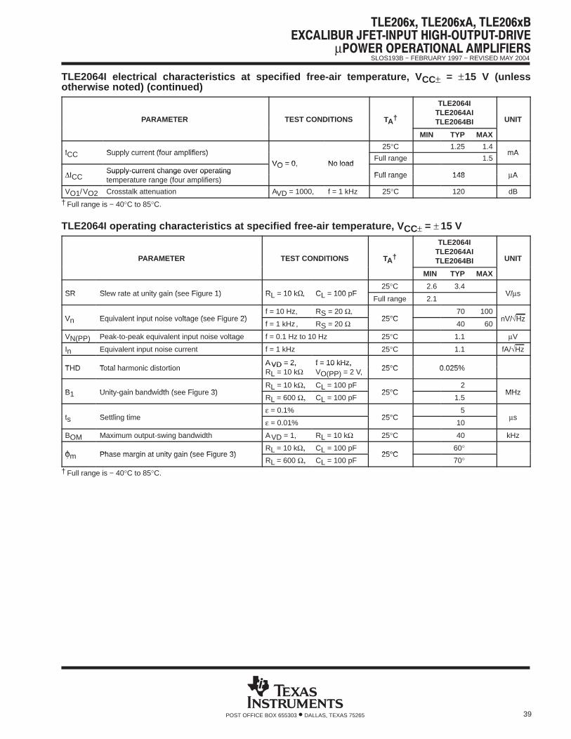
µ
SLOS193B − FEBRUARY 1997 − REVISED MAY 2004
39POST OFFICE BOX 655303 • DALLAS, TEXAS 75265
TLE2064I electrical characteristics at specified free-air temperature, V CC± = ±15 V (unlessotherwise noted) (continued)
PARAMETER TEST CONDITIONS TA†
TLE2064ITLE2064AITLE2064BI UNITA
MIN TYP MAX
ICC Supply current (four amplifiers)25°C 1.25 1.4
mAICC Supply current (four amplifiers)VO = 0, No load
Full range 1.5mA
∆ICCSupply-current change over operating
VO = 0, No load
Full range 148 µA∆ICCSupply-current change over operating temperature range (four amplifiers)
Full range 148 µA
VO1/VO2 Crosstalk attenuation AVD = 1000, f = 1 kHz 25°C 120 dB
† Full range is − 40°C to 85°C.
TLE2064I operating characteristics at specified free-air temperature, V CC± = ± 15 V
PARAMETER TEST CONDITIONS TA†
TLE2064ITLE2064AITLE2064BI UNITA
MIN TYP MAX
SR Slew rate at unity gain (see Figure 1) RL = 10 kΩ, CL = 100 pF25°C 2.6 3.4
V/ sSR Slew rate at unity gain (see Figure 1) RL = 10 kΩ, CL = 100 pFFull range 2.1
V/µs
Vn Equivalent input noise voltage (see Figure 2)f = 10 Hz, RS = 20 Ω,
25°C70 100
nV/√HzVn Equivalent input noise voltage (see Figure 2)f = 1 kHz , RS = 20 Ω
25°C40 60
nV/√Hz
VN(PP) Peak-to-peak equivalent input noise voltage f = 0.1 Hz to 10 Hz 25°C 1.1 µV
In Equivalent input noise current f = 1 kHz 25°C 1.1 fA/√Hz
THD Total harmonic distortionAVD = 2, f = 10 kHz,
25°C 0.025%THD Total harmonic distortionAVD = 2,RL = 10 kΩ
f = 10 kHz,VO(PP) = 2 V, 25°C 0.025%
B1 Unity-gain bandwidth (see Figure 3)RL = 10 kΩ, CL = 100 pF
25°C2
MHzB1 Unity-gain bandwidth (see Figure 3)RL = 600 Ω, CL = 100 pF
25°C1.5
MHz
ts Settling timeε = 0.1%
25°C5
sts Settling timeε = 0.01%
25°C10
µs
BOM Maximum output-swing bandwidth AVD = 1, RL = 10 kΩ 25°C 40 kHz
φm Phase margin at unity gain (see Figure 3)RL = 10 kΩ, CL = 100 pF
25°C60°
φm Phase margin at unity gain (see Figure 3)RL = 600 Ω, CL = 100 pF
25°C70°
† Full range is − 40°C to 85°C.
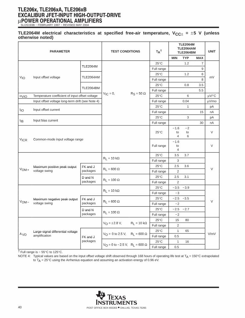
µ
SLOS193B − FEBRUARY 1997 − REVISED MAY 2004
40 POST OFFICE BOX 655303 • DALLAS, TEXAS 75265
TLE2064M electrical characteristics at specified free-air temperature, V CC± = ±5 V (unlessotherwise noted)
PARAMETER TEST CONDITIONS TA†
TLE2064MTLE2064AMTLE2064BM UNITA
MIN TYP MAX
TLE2064M25°C 1.2 7
TLE2064MFull range 9
VIO Input offset voltage TLE2064AM25°C 1.2 6
mVVIO Input offset voltage TLE2064AMFull range 8
mV
TLE2064BM25°C 0.8 3.5
TLE2064BM
VIC = 0, RS = 50 ΩFull range 5.5
αVIO Temperature coefficient of input offset voltageVIC = 0, RS = 50 Ω
25°C 6 µV/°C
Input offset voltage long-term drift (see Note 4) Full range 0.04 µV/mo
IIO Input offset current25°C 1 pA
IIO Input offset currentFull range 15 nA
IIB Input bias current25°C 3 pA
IIB Input bias currentFull range 30 nA
VICR Common-mode input voltage range
25°C−1.6
to4
−2to6
V
VICR Common-mode input voltage range
Full range−1.6
to4
V
RL = 10 kΩ25°C 3.5 3.7
RL = 10 kΩFull range 3
VOM+Maximum positive peak output FK and J
RL = 600 Ω25°C 2.5 3.6
VVOM+Maximum positive peak outputvoltage swing
FK and Jpackages RL = 600 Ω
Full range 2Vvoltage swing
D and NRL = 100 Ω
25°C 2.5 3.1D and Npackages RL = 100 Ω
Full range 2
RL = 10 kΩ25°C −3.5 −3.9
RL = 10 kΩFull range −3
VOM−Maximum negative peak output FK and J
RL = 600 Ω25°C −2.5 −3.5
VVOM−Maximum negative peak outputvoltage swing
FK and Jpackages RL = 600 Ω
Full range −2Vvoltage swing
D and NRL = 100 Ω
25°C −2.5 −2.7D and Npackages RL = 100 Ω
Full range −2
VO = ±2.8 V, RL = 10 kΩ25°C 15 80
VO = ±2.8 V, RL = 10 kΩFull range 2
AVDLarge-signal differential voltage
VO = 0 to 2.5 V, RL = 600 Ω25°C 1 65
V/mVAVDLarge-signal differential voltageamplification FK and J
VO = 0 to 2.5 V, RL = 600 ΩFull range 0.5
V/mVamplification FK and Jpackages
VO = 0 to −2.5 V, RL = 600 Ω25°C 1 16packages
VO = 0 to −2.5 V, RL = 600 ΩFull range 0.5
† Full range is − 55°C to 125°C.NOTE 4: Typical values are based on the input offset voltage shift observed through 168 hours of operating life test at TA = 150°C extrapolated
to TA = 25°C using the Arrhenius equation and assuming an activation energy of 0.96 eV.

µ
SLOS193B − FEBRUARY 1997 − REVISED MAY 2004
41POST OFFICE BOX 655303 • DALLAS, TEXAS 75265
TLE2064M electrical characteristics at specified free-air temperature, V CC± = ±5 V (unlessotherwise noted) continued)
PARAMETER TEST CONDITIONS TA†
TLE2064MTLE2064AMTLE2064BM UNITA
MIN TYP MAX
VO = 0 to 2 V, RL = 100 Ω25°C 0.75 45
AVDLarge-signal differential voltage D and N
VO = 0 to 2 V, RL = 100 ΩFull range 0.25
V/mVAVDLarge-signal differential voltageamplification
D and Npackages
VO = 0 to −2 V, RL = 100 Ω25°C 0.4 3
V/mVamplification packagesVO = 0 to −2 V, RL = 100 Ω
Full range 0.15
ri Input resistance 25°C 1012 Ω
ci Input capacitance 25°C 4 pF
zo Open-loop output impedance IO = 0 25°C 560 Ω
CMRR Common-mode rejection ratio VIC = VICRmin, RS = 50 Ω25°C 65 82
dBCMRR Common-mode rejection ratio VIC = VICRmin, RS = 50 ΩFull range 60
dB
kSVR Supply-voltage rejection ratio (∆VCC /∆VIO)VCC± = ±5 V to ±15 V, 25°C 75 93
dBkSVR Supply-voltage rejection ratio (∆VCC± /∆VIO)VCC± = ±5 V to ±15 V,RS = 50 Ω Full range 65
dB
ICC Supply current (four amplifiers)25°C 1.12 1.3
mAICC Supply current (four amplifiers)VO = 0, No load
Full range 1.3mA
∆ICCSupply-current change over operatingtemperature range (four amplifiers)
VO = 0, No load
Full range 144 µA
VO1/VO2 Crosstalk attenuation AVD = 1000, f = 1 kHz 25°C 120 dB
† Full range is −55°C to 125°C.
TLE2064M operating characteristics, V CC± = ±5 V, TA = 25°C
PARAMETER TEST CONDITIONS
TLE2064MTLE2064AMTLE2064BM UNIT
MIN TYP MAX
SR Slew rate at unity gain (see Figure 1) RL = 10 kΩ, CL = 100 pF 3.4 V/µs
Vn Equivalent input noise voltage (see Figure 2)f = 10 Hz, RS = 20 Ω 59
nV/√HzVn Equivalent input noise voltage (see Figure 2)f = 1 kHz , RS = 20 Ω 43
nV/√Hz
VN(PP) Peak-to-peak equivalent input noise voltage f = 0.1 Hz to 10 Hz 1.1 µV
In Equivalent input noise current f = 1 kHz 1 fA/√Hz
THD Total harmonic distortionAVD = 2, f = 10 kHz,
0.025%THD Total harmonic distortionAVD = 2,VO(PP) = 2 V,
f = 10 kHz, RL = 10 kΩ 0.025%
B1 Unity-gain bandwidth (see Figure 3)RL = 10 kΩ, CL = 100 pF 1.8
MHzB1 Unity-gain bandwidth (see Figure 3)RL = 600 Ω, CL = 100 pF 1.3
MHz
ts Settling timeε = 0.1% 5
sts Settling timeε = 0.01% 10
µs
BOM Maximum output-swing bandwidth AVD = 1, RL = 10 kΩ 140 kHz
φm Phase margin at unity gain (see Figure 3)RL = 10 kΩ, CL = 100 pF 58°
φm Phase margin at unity gain (see Figure 3)RL = 600 Ω, CL = 100 pF 75°
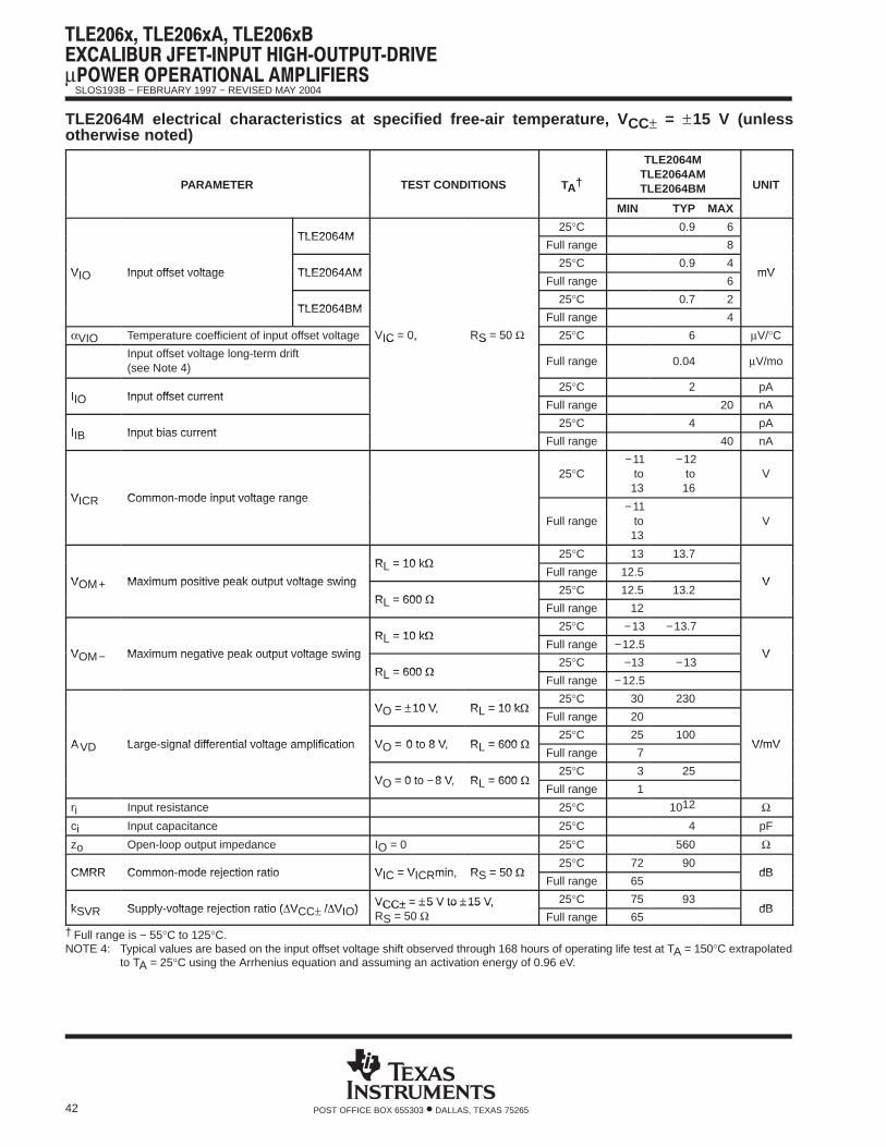
µ
SLOS193B − FEBRUARY 1997 − REVISED MAY 2004
42 POST OFFICE BOX 655303 • DALLAS, TEXAS 75265
TLE2064M electrical characteristics at specified free-air temperature, V CC± = ±15 V (unlessotherwise noted)
PARAMETER TEST CONDITIONS TA†
TLE2064MTLE2064AMTLE2064BM UNITA
MIN TYP MAX
TLE2064M25°C 0.9 6
TLE2064MFull range 8
VIO Input offset voltage TLE2064AM25°C 0.9 4
mVVIO Input offset voltage TLE2064AMFull range 6
mV
TLE2064BM25°C 0.7 2
TLE2064BMFull range 4
αVIO Temperature coefficient of input offset voltage VIC = 0, RS = 50 Ω 25°C 6 µV/°CInput offset voltage long-term drift (see Note 4)
VIC = 0, RS = 50
Full range 0.04 µV/mo
IIO Input offset current25°C 2 pA
IIO Input offset currentFull range 20 nA
IIB Input bias current25°C 4 pA
IIB Input bias currentFull range 40 nA
VICR Common-mode input voltage range
25°C−11
to13
−12to16
V
VICR Common-mode input voltage range
Full range−11
to13
V
RL = 10 kΩ25°C 13 13.7
VOM+ Maximum positive peak output voltage swing
RL = 10 kΩFull range 12.5
VVOM+ Maximum positive peak output voltage swing
RL = 600 Ω25°C 12.5 13.2
V
RL = 600 ΩFull range 12
RL = 10 kΩ25°C −13 −13.7
VOM− Maximum negative peak output voltage swing
RL = 10 kΩFull range −12.5
VVOM− Maximum negative peak output voltage swing
RL = 600 Ω25°C −13 −13
V
RL = 600 ΩFull range −12.5
VO = ±10 V, RL = 10 kΩ25°C 30 230
VO = ±10 V, RL = 10 kΩFull range 20
AVD Large-signal differential voltage amplification VO = 0 to 8 V, RL = 600 Ω25°C 25 100
V/mVAVD Large-signal differential voltage amplification VO = 0 to 8 V, RL = 600 ΩFull range 7
V/mV
VO = 0 to −8 V, RL = 600 Ω25°C 3 25
VO = 0 to −8 V, RL = 600 ΩFull range 1
ri Input resistance 25°C 1012 Ωci Input capacitance 25°C 4 pF
zo Open-loop output impedance IO = 0 25°C 560 Ω
CMRR Common-mode rejection ratio VIC = VICRmin, RS = 50 Ω25°C 72 90
dBCMRR Common-mode rejection ratio VIC = VICRmin, RS = 50 ΩFull range 65
dB
kSVR Supply-voltage rejection ratio (∆VCC /∆VIO)VCC± = ±5 V to ±15 V, 25°C 75 93
dBkSVR Supply-voltage rejection ratio (∆VCC± /∆VIO)VCC± = ±5 V to ±15 V,RS = 50 Ω Full range 65
dB
† Full range is − 55°C to 125°C.NOTE 4: Typical values are based on the input offset voltage shift observed through 168 hours of operating life test at TA = 150°C extrapolated
to TA = 25°C using the Arrhenius equation and assuming an activation energy of 0.96 eV.
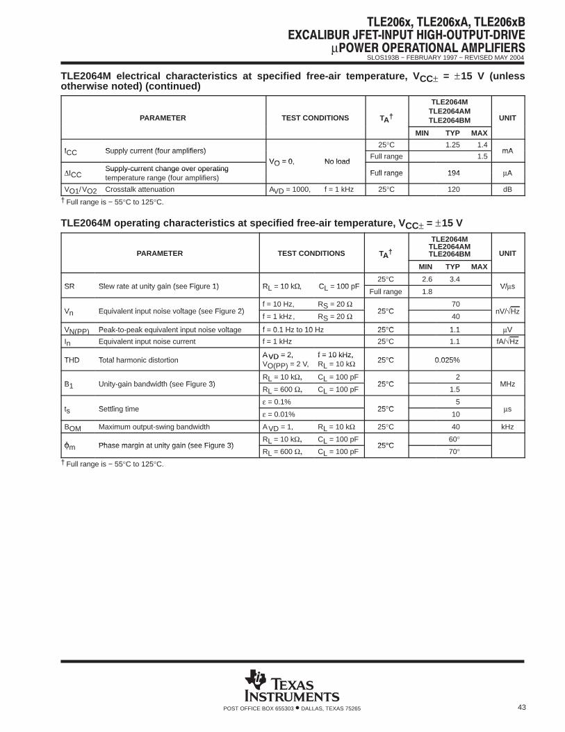
µ
SLOS193B − FEBRUARY 1997 − REVISED MAY 2004
43POST OFFICE BOX 655303 • DALLAS, TEXAS 75265
TLE2064M electrical characteristics at specified free-air temperature, V CC± = ±15 V (unlessotherwise noted) (continued)
PARAMETER TEST CONDITIONS TA†
TLE2064MTLE2064AMTLE2064BM UNITA
MIN TYP MAX
ICC Supply current (four amplifiers)25°C 1.25 1.4
mAICC Supply current (four amplifiers)VO = 0, No load
Full range 1.5mA
∆ICCSupply-current change over operating
VO = 0, No load
Full range 194 µA∆ICCSupply-current change over operating temperature range (four amplifiers)
Full range 194 µA
VO1/VO2 Crosstalk attenuation AVD = 1000, f = 1 kHz 25°C 120 dB
† Full range is − 55°C to 125°C.
TLE2064M operating characteristics at specified free-air temperature, V CC± = ±15 V
PARAMETER TEST CONDITIONS TA†
TLE2064MTLE2064AMTLE2064BM UNITPARAMETER TEST CONDITIONS TA
MIN TYP MAX
UNIT
SR Slew rate at unity gain (see Figure 1) RL = 10 kΩ, CL = 100 pF25°C 2.6 3.4
V/ sSR Slew rate at unity gain (see Figure 1) RL = 10 kΩ, CL = 100 pFFull range 1.8
V/µs
Vn Equivalent input noise voltage (see Figure 2)f = 10 Hz, RS = 20 Ω
25°C70
nV/√HzVn Equivalent input noise voltage (see Figure 2)f = 1 kHz , RS = 20 Ω
25°C40
nV/√Hz
VN(PP) Peak-to-peak equivalent input noise voltage f = 0.1 Hz to 10 Hz 25°C 1.1 VVN(PP) Peak-to-peak equivalent input noise voltage f = 0.1 Hz to 10 Hz 25°C 1.1 µV
In Equivalent input noise current f = 1 kHz 25°C 1.1 fA/√Hz
THD Total harmonic distortionAVD = 2, f = 10 kHz,
25°C 0.025%THD Total harmonic distortionAVD = 2,VO(PP) = 2 V,
f = 10 kHz,RL = 10 kΩ 25°C 0.025%
B1 Unity-gain bandwidth (see Figure 3)RL = 10 kΩ, CL = 100 pF
25°C2
MHzB1 Unity-gain bandwidth (see Figure 3)RL = 600 Ω, CL = 100 pF
25°C1.5
MHz
ts Settling timeε = 0.1%
25°C5
sts Settling timeε = 0.01%
25°C10
µs
BOM Maximum output-swing bandwidth AVD = 1, RL = 10 kΩ 25°C 40 kHz
φm Phase margin at unity gain (see Figure 3)RL = 10 kΩ, CL = 100 pF
25°C60°
φm Phase margin at unity gain (see Figure 3)RL = 600 Ω, CL = 100 pF
25°C70°
† Full range is − 55°C to 125°C.

µ
SLOS193B − FEBRUARY 1997 − REVISED MAY 2004
44 POST OFFICE BOX 655303 • DALLAS, TEXAS 75265
TLE2064Y electrical characteristics at V CC± = ±15 V, TA = 25°C (unless otherwise noted)
PARAMETER TEST CONDITIONSTLE2064Y
UNITPARAMETER TEST CONDITIONSMIN TYP MAX
UNIT
VIO Input offset voltage 0.9 6 mV
∝VIO Input offset voltage long-term drift (see Note 4)VIC = 0, RS = 50 Ω
0.04 µV/mo
IIO Input offset currentVIC = 0, RS = 50 Ω
2 pA
IIB Input bias current 4 pA
VICR Common-mode input voltage range−11
to13
−12to16
V
VOM+ Maximum positive peak output voltage swingRL = 10 kΩ 13.2 13.7
VVOM+ Maximum positive peak output voltage swingRL = 600 Ω 12.5 13.2
V
VOM− Maximum negative peak output voltage swingRL = 10 kΩ −13.2 −13.7 V
VOM− Maximum negative peak output voltage swingRL = 600 Ω 12.5 13 V
VO = ±10 V, RL = 10 kΩ 30 230
AVD Large-signal differential voltage amplification VO = 0 to 8 V, RL = 600 Ω 25 100 V/mVAVD Large-signal differential voltage amplification
VO = 0 to −8 V, RL = 600 Ω 3 25
V/mV
ri Input resistance 1012 Ω
ci Input capacitance 4 pF
zo Open-loop output impedance IO = 0 560 Ω
CMRR Common-mode rejection ratioRS = 50 Ω,VIC = VICRmin,
72 90 dB
kSVR Supply-voltage rejection ratio (∆VCC± /∆VIO)VCC± = ±5 V to ±15 V,RS = 50 Ω 75 93 dB
ICC Supply current VO = 0, No load 1.25 1.4 mA
VO1/VO2 Crosstalk attenuation AVD = 1000, f = 1 kHz 120 dB
NOTE 4: Typical values are based on the input offset voltage shift observed through 168 hours of operating life test at TA = 150°C extrapolatedto TA = 25°C using the Arrhenius equation and assuming an activation energy of 0.96 eV.
TLE2064Y operating characteristics at V CC± = ±15 V, TA = 25°C
PARAMETER TEST CONDITIONSTLE2064Y
UNITPARAMETER TEST CONDITIONSMIN TYP MAX
UNIT
SR Slew rate at unity gain (see Figure 1) RL = 10 kΩ, CL = 100 pF 2.6 3.4 V/µs
Vn Equivalent input noise voltage (see Figure 2)f = 10 Hz, RS = 20 Ω 70
nV/√HzVn Equivalent input noise voltage (see Figure 2)f = 1 kHz , RS = 20 Ω 40
nV/√Hz
VN(PP) Peak-to-peak equivalent input noise voltage f = 0.1 Hz to 10 Hz 1.1 µV
In Equivalent input noise current f = 1 kHz 1.1 fA/√Hz
THD Total harmonic distortionAVD = 2, f = 10 kHz,
0.025%THD Total harmonic distortionAVD = 2,VO(PP) = 2 V,
f = 10 kHz, RL = 10 kΩ 0.025%
B1 Unity-gain bandwidth (see Figure 3)RL = 10 kΩ, CL = 100 pF 2
MHzB1 Unity-gain bandwidth (see Figure 3)RL = 600 Ω, CL = 100 pF 1.5
MHz
ts Settling timeε = 0.1% 5
sts Settling timeε = 0.01% 10
µs
BOM Maximum output-swing bandwidth AVD = 1, RL = 10 kΩ 40 kHz
φm Phase margin at unity gain (see Figure 3)RL = 10 kΩ, CL = 100 pF 60°
φm Phase margin at unity gain (see Figure 3)RL = 600 Ω, CL = 100 pF 70°

µ
SLOS193B − FEBRUARY 1997 − REVISED MAY 2004
45POST OFFICE BOX 655303 • DALLAS, TEXAS 75265
PARAMETER MEASUREMENT INFORMATION
Figure 1. Slew-Rate Test Circuit
RL(see Note A)
CL
VO
VCC−
VI +
−
VCC+
NOTE A: CL includes fixture capacitance.
Figure 2. Noise-Voltage Test Circuit
VO
RSRS
2 kΩ
VCC−
VCC+
+
−
VO
RLCL(see Note A)
10 kΩ
100 ΩVI
VCC−
VCC+
+
−
NOTE A: CL includes fixture capacitance.
Figure 3. Unity-Gain Bandwidth and Phase-Margin Test Circuit
typical values
Typical values presented in this data sheet represent the median (50% point) of device parametric performance.
input bias and offset current
At the picoampere bias current level typical of the TLE206x, TLE2064xA, and TLE206xB, accuratemeasurement of the bias current becomes difficult. Not only does this measurement require a picoammeter,but test socket leakages can easily exceed the actual device bias currents. To accurately measure these smallcurrents, Texas Instruments uses a two-step process. The socket leakage is measured using picoammeterswith bias voltages applied but with no device in the socket. The device is then inserted into the socket and asecond test that measures both the socket leakage and the device input bias current is performed. The twomeasurements are then subtracted algebraically to determine the bias current of the device.

µ
SLOS193B − FEBRUARY 1997 − REVISED MAY 2004
46 POST OFFICE BOX 655303 • DALLAS, TEXAS 75265
TYPICAL CHARACTERISTICS
Table of Graphs
FIGURE
VIO Input offset voltage Distribution 4, 5, 6
IIB Input bias currentvs Common-mode input voltagevs Free-air temperature
78
IIO Input offset current vs Free-air temperature 8
VICR Common-mode input voltage vs Free-air temperature 9
VOM Maximum peak output voltagevs Output currentvs Supply voltage
10, 1112, 13, 14
VO(PP) Maximum peak-to-peak output voltagevs Frequencyvs Load resistance
15, 1617
AVD Large-signal differential voltage amplificationvs Frequencyvs Free-air temperature
1819
IOS Short-circuit output currentvs Elasped timevs Free-air temperature
2021
zo Output impedance vs Frequency 22, 23
CMRR Common-mode rejection ratio vs Frequency 24
ICC Supply currentvs Supply voltagevs Free-air temperature
25, 26, 2728, 29, 30
Voltage-follower small-signal pulse response vs Time 31, 32
Voltage-follower large-signal pulse response vs Time 33, 34
Noise voltage (referred to input) 0.1 to 10 Hz 35
Vn Equivalent input noise voltage vs Frequency 36
THD Total harmonic distortion vs Frequency 37, 38
B1 Unity-gain bandwidthvs Supply voltagevs Free-air temperature
3940
φm Phase marginvs Supply voltagevs Load capacitancevs Free-air temperature
414243
Phase shift vs Frequency 18

µ
SLOS193B − FEBRUARY 1997 − REVISED MAY 2004
47POST OFFICE BOX 655303 • DALLAS, TEXAS 75265
TYPICAL CHARACTERISTICS
Figure 4
TLE2061DISTRIBUTION OF
INPUT OFFSET VOLTAGE
43210−1−2−3−4
VIO − Input Offset Voltage − mV
Per
cent
age
of A
mpl
ifier
s −
%
0
5
10
15
P PackageTA = 25°CVCC± = ±15 V736 Amplifiers Tested From 3 Wafer Lots
Figure 5VIO − Input Offset Voltage − mV
10
5
0− 2 −1 0 1
Per
cent
age
of A
mpl
ifier
s −
%
TLE2062DISTRIBUTION OF
INPUT OFFSET VOLTAGE
2 3 4
151836 Amplifiers Tested From 1 Wafer LotVCC± = ±15 VTA = 25°CP Package
−3−4
Figure 6
TLE2064DISTRIBUTION OF
INPUT OFFSET VOLTAGE20
15
10
5
N PackageTA = 25°CVCC± = ±15 V
86420− 2− 4− 6− 8
VIO − Input Offset Voltage − mV
Per
cent
age
of A
mpl
ifier
s −
%
0
ÎÎÎÎÎÎÎÎÎÎÎÎÎÎÎÎÎÎÎÎÎÎÎÎ
2792 Amplifiers Tested From 2 Wafer Lots
Figure 7
− In
put B
ias
Cur
rent
− n
AI IB
1.5
1
0.5
TA = 25°CVID = 0
VCC± = ±15 V
VIC − Common-Mode Input Voltage − V
− 20 − 15 − 10 − 5 0 5 10 15 20
2
0
INPUT BIAS CURRENTvs
COMMON-MODE INPUT VOLTAGE

µ
SLOS193B − FEBRUARY 1997 − REVISED MAY 2004
48 POST OFFICE BOX 655303 • DALLAS, TEXAS 75265
TYPICAL CHARACTERISTICS †
Figure 8
INPUT BIAS CURRENTAND INPUT OFFSET CURRENT
vsFREE-AIR TEMPERATURE
TA − Free-Air Temperature − °C10585654525
105
104
103
102
101
100
VIC = 0VCC± = ±15 V
− In
put B
ias
and
Inpu
t Offs
et C
urre
nts
− pA
I IB
and
I IO
ÎÎÎÎ
IIOÎÎÎÎ
IIB
125
Figure 9
COMMON-MODE INPUT VOLTAGEvs
FREE-AIR TEMPERATURE
1251007550250− 25− 50− 75
TA − Free-Air Temperature − °C
VCC +
VCC +
VCC −
VCC −
VCC − + 2
+ 3
+ 4
VCC +
+ 1
+ 2
− C
omm
on-M
ode
Inpu
t Vol
tage
− V
VIC
ÎÎVIC +
ÎÎÎÎÎÎ
VIC −
Figure 10
MAXIMUM POSITIVE PEAKOUTPUT VOLTAGE
vsOUTPUT CURRENT
− M
axim
um P
ositi
ve P
eak
Out
put V
olta
ge −
VV O
M+
− 60− 50− 40− 30− 20− 100
IO − Output Current − mA
0
2
4
6
8
10
12
14
16
18
20
VCC± = ± 5 V
VCC± = ±15 V
ÎÎÎÎÎÎÎÎ
TA = 25°C
Figure 11
MAXIMUM NEGATIVE PEAKOUTPUT VOLTAGE
vsOUTPUT CURRENT
− M
axim
um N
egat
ive
Pea
k O
utpu
t Vol
tage
− V
VO
M−
30 35
VCC± = ±15 V
VCC± = ±5 V
IO − Output Current − mA
0 5 10 15 20 25 40
− 20
− 18
− 16
− 14
− 12
− 10
− 8
− 6
− 4
− 2
0
ÎÎÎÎÎÎÎÎ
TA = 25°C
† Data at high and low temperatures are applicable only within the rated operating free-air temperature ranges of the various devices.
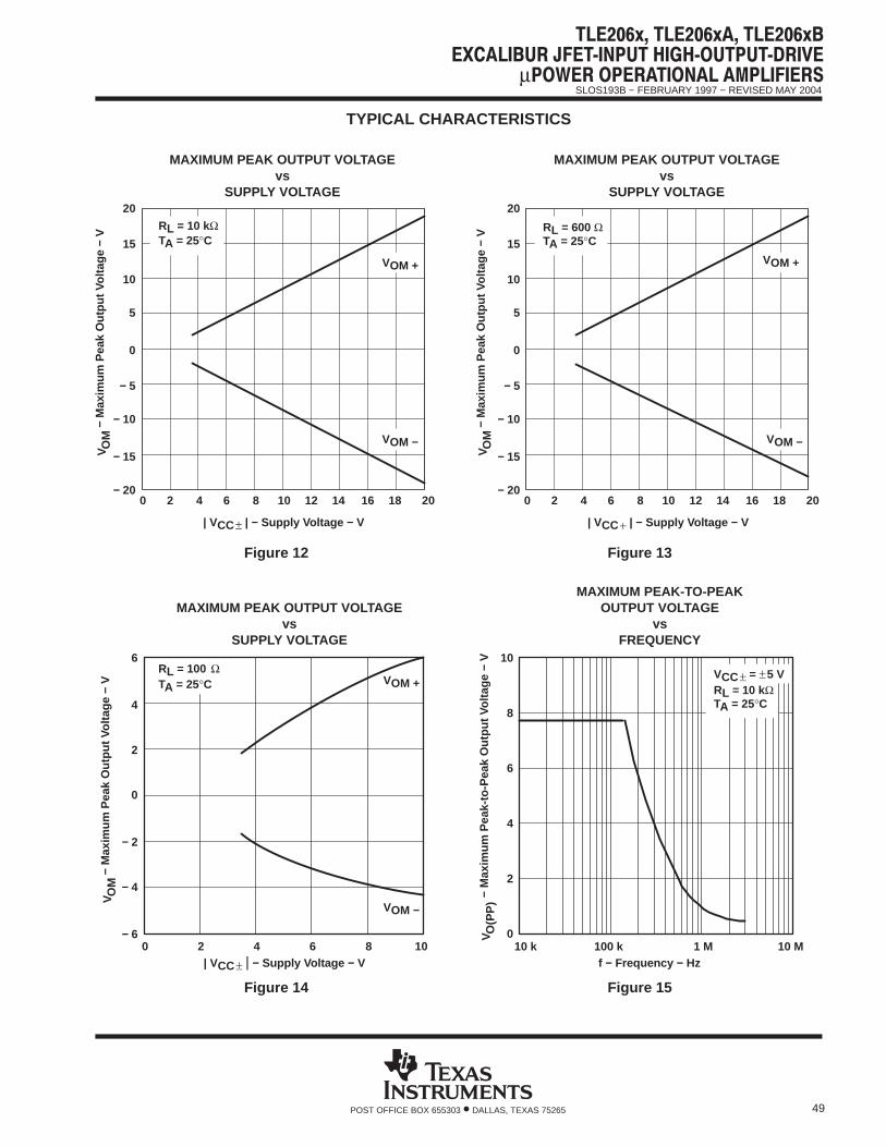
µ
SLOS193B − FEBRUARY 1997 − REVISED MAY 2004
49POST OFFICE BOX 655303 • DALLAS, TEXAS 75265
TYPICAL CHARACTERISTICS
Figure 12
MAXIMUM PEAK OUTPUT VOLTAGEvs
SUPPLY VOLTAGE
− M
axim
um P
eak
Out
put V
olta
ge −
VV O
M
20181614121086420
| VCC± | − Supply Voltage − V
− 20
− 15
− 10
− 5
0
5
10
15
20
VOM −
VOM +
TA = 25°CRL = 10 kΩ
Figure 13
MAXIMUM PEAK OUTPUT VOLTAGEvs
SUPPLY VOLTAGE
RL = 600 ΩTA = 25°C
VOM +
VOM −
20
15
10
5
0
− 5
− 10
− 15
− 20
| VCC+ | − Supply Voltage − V
0 2 4 6 8 10 12 14 16 18 20
− M
axim
um P
eak
Out
put V
olta
ge −
VV O
M
Figure 14
MAXIMUM PEAK OUTPUT VOLTAGEvs
SUPPLY VOLTAGE
− M
axim
um P
eak
Out
put V
olta
ge −
VV O
M
VOM −
VOM +TA = 25°CRL = 100 Ω
1086420| VCC± | − Supply Voltage − V
− 6
− 4
− 2
0
2
4
6
Figure 15
MAXIMUM PEAK-TO-PEAKOUTPUT VOLTAGE
vsFREQUENCY
− M
axim
um P
eak-
to-P
eak
Out
put V
olta
ge −
VV O
(PP
)
TA = 25°CRL = 10 kΩVCC± = ±5 V
10
8
6
10 k 100 k 1 M 10 Mf − Frequency − Hz
4
2
0

µ
SLOS193B − FEBRUARY 1997 − REVISED MAY 2004
50 POST OFFICE BOX 655303 • DALLAS, TEXAS 75265
TYPICAL CHARACTERISTICS †
Figure 16
− M
axim
um P
eak-
to-P
eak
Out
put V
olta
ge −
VV O
(PP
)
MAXIMUM PEAK-TO-PEAKOUTPUT VOLTAGE
vsFREQUENCY
15
RL = 10 kΩVCC± = ±15 V
30
25
20
10 k 100 k 1 M 10 M
f − Frequency − Hz
10
5
0
ÎÎÎÎÎÎÎÎ
TA = 25°C
Figure 17
MAXIMUM PEAK-TO-PEAKOUTPUT VOLTAGE
vsLOAD RESISTANCE
RL − Load Resistance − Ω
10 k1 k100100
2
4
6
8
10ÎÎÎÎÎÎÎÎÎÎÎÎÎÎÎÎÎÎ
VCC± = ±5 VTA = 25°C
− M
axim
um P
eak-
to-P
eak
Out
put V
olta
ge −
VV O
(PP
)
− La
rge-
Sig
nal D
Iffer
entia
l Vol
tage
Am
plifi
catio
n −
dBA
VD
LARGE-SIGNAL DIFFERENTIAL VOLTAGEAMPLIFICATION AND PHASE SHIFT
vsFREQUENCY
Pha
se S
hift
TA = 25°CCL = 100 pFRL = 10 kΩVCC± = ±15 V
Phase Shift
60°
80°
100°
120°
140°
160°
180°
200°10 M1 M100 k10 k1 k1001010.1
f − Frequency − Hz
−20
0
20
40
60
80
100
120
ÎÎÎAVD
Figure 18
LARGE-SIGNAL VOLTAGE AMPLIFICATIONvs
FREE-AIR TEMPERATURE
RL = 10 kΩ
VCC± = ±5 V
VCC± = ±15 V
TA − Free-Air Temperature − °C
1251007550250− 25− 50− 75
350
300
250
200
150
100
50
0
400
− La
rge-
Sig
nal D
Iffer
entia
l Vol
tage
Am
plifi
catio
n −
V/m
VA
VD
Figure 19
† Data at high and low temperatures are applicable only within the rated operating free-air temperature ranges of the various devices.

µ
SLOS193B − FEBRUARY 1997 − REVISED MAY 2004
51POST OFFICE BOX 655303 • DALLAS, TEXAS 75265
TYPICAL CHARACTERISTICS †
Figure 20
− S
hort
-Circ
uit O
utpu
t Cur
rent
− m
AI O
S
SHORT-CIRCUIT OUTPUT CURRENTvs
ELAPSED TIME
VID = 100 mV
VO = 0
TA = 25°CVCC± = ±15 V
VID = − 100 mV
6050403020100
t − Elapsed Time − s
− 80
− 60
− 40
− 20
0
20
40
60
80
Figure 21
SHORT-CIRCUIT OUTPUT CURRENTvs
FREE-AIR TEMPERATURE
VID = − 100 mV
VID = 100 mV
VO = 0
VCC± = ±15 V80
− 80
− 60
− 40
− 20
0
20
40
60
− 75 − 50 − 25 0 25 50 75 100 125
TA − Free-Air Temperature − °C
− S
hort
-Circ
uit O
utpu
t Cur
rent
− m
AI O
S
Figure 22
TA = 25°CVCC± = ±15 V
AVD = 10
f − Frequency − Hz
1 M100 k10 k1 k10010
− O
utpu
t Im
peda
nce
−
0.001
0.01
0.1
1
10
100
1000
ÁÁÁÁ
z o
ÁÁÁÁ
Ω AVD = 100
ÎÎÎÎÎÎÎÎ
AVD = 1
TLE2061OUTPUT IMPEDANCE
vsFREQUENCY
Figure 23
− O
utpu
t Im
peda
nce
−z o
35
30
25
20
15
10
5
TA = 25°CVCC± = ±15 V
AVD = 100
f − Frequency − Hz
1 M100 k10 k1 k1000
Ω
ÎÎÎÎÎÎÎÎAVD = 1
ÎÎÎÎAVD = 10
10 M
TLE2062 AND TLE2064OUTPUT IMPEDANCE
vsFREQUENCY
† Data at high and low temperatures are applicable only within the rated operating free-air temperature ranges of the various devices.
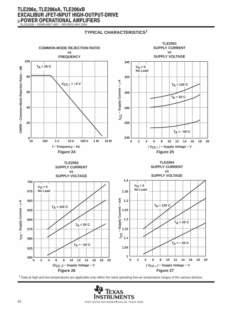
µ
SLOS193B − FEBRUARY 1997 − REVISED MAY 2004
52 POST OFFICE BOX 655303 • DALLAS, TEXAS 75265
TYPICAL CHARACTERISTICS †
Figure 24
COMMON-MODE REJECTION RATIOvs
FREQUENCY
CM
RR
− C
omm
on-M
ode
Rej
ectio
n R
atio
− d
B
10 100 1 k 10 k 100 k 1 M
f − Frequency − Hz
10 M0
20
40
60
80
100
TA = 25°C
ÎÎÎÎÎÎÎÎÎÎ
VCC± = ±5 V
Figure 25
Aµ
2
− S
uppl
y C
urre
nt −
I CC
No LoadVO = 0
TA = 125°C
TA = 25°C
TA = −55°C
2018161412108640
| VCC± | − Supply Voltage − V
340
240
260
280
300
320
TLE2061SUPPLY CURRENT
vsSUPPLY VOLTAGE
Figure 26|VCC±| − Supply Voltage − V
ICC
− S
uppl
y C
urre
nt −
xA
CC
I
600
575
525
5000 2 4 6 8 10 12
625
675
700
14 16 18 20
550
650Aµ
TA = 25°C
TA = 125°C
TA = −55°C
VO = 0No Load
TLE2062SUPPLY CURRENT
vsSUPPLY VOLTAGE
Figure 27
− S
uppl
y C
urre
nt −
mA
I CC
1
1.1
1.2
1.3
1.4
No LoadVO = 0
TA = 125°C
TA = 25°C
TA = − 55°C
| VCC± | − Supply Voltage − V
20181614121086420
1.25
1.35
1.05
1.15
TLE2064SUPPLY CURRENT
vsSUPPLY VOLTAGE
† Data at high and low temperatures are applicable only within the rated operating free-air temperature ranges of the various devices.

µ
SLOS193B − FEBRUARY 1997 − REVISED MAY 2004
53POST OFFICE BOX 655303 • DALLAS, TEXAS 75265
TYPICAL CHARACTERISTICS †
Figure 28
Aµ
−75
− S
uppl
y C
urre
nt −
I CC
VCC± = ±5 V
VO = 0No Load
240
260
280
300
320
340
1251007550250−25−50
TA − Free-Air Temperature − °C
260
280
300
ÎÎÎÎÎÎÎÎÎÎ
VCC± = ±15 V
TLE2061SUPPLY CURRENT
vsFREE-AIR TEMPERATURE
Figure 29
− 75 − 50 − 25 0 25 50 75 100 125
VCC± = ±5 V
VCC± = ±15 V
VO = 0No Load
600
575
525
500
625
675
700
550
650
TA − Free-Air Temperature − °C
ICC
− S
uppl
y C
urre
nt −
xA
CC
IA
µ
TLE2062SUPPLY CURRENT
vsFREE-AIR TEMPERATURE
Figure 30
− S
uppl
y C
urre
nt −
mA
I CC
1.4
1.3
1.2
1.1ÎÎÎÎÎÎÎÎÎÎ
VCC± = ±5 V
ÎÎÎÎÎVCC± = ±15 V
VO = 0No Load
TA − Free-Air Temperature − °C
11251007550250− 25− 50− 75
1.25
1.35
1.05
1.15
TLE2064SUPPLY CURRENT
vsFREE-AIR TEMPERATURE
Figure 31
− O
utpu
t Vol
tage
− m
VV
O
VOLTAGE-FOLLOWERSMALL-SIGNAL
PULSE RESPONSE
t − Time − µs210
− 100
− 50
0
50
100
VCC± = ±5 VRL = 10 kΩCL = 100 pFTA = 25°CSee Figure 1
2.51.50.5
† Data at high and low temperatures are applicable only within the rated operating free-air temperature ranges of the various devices.
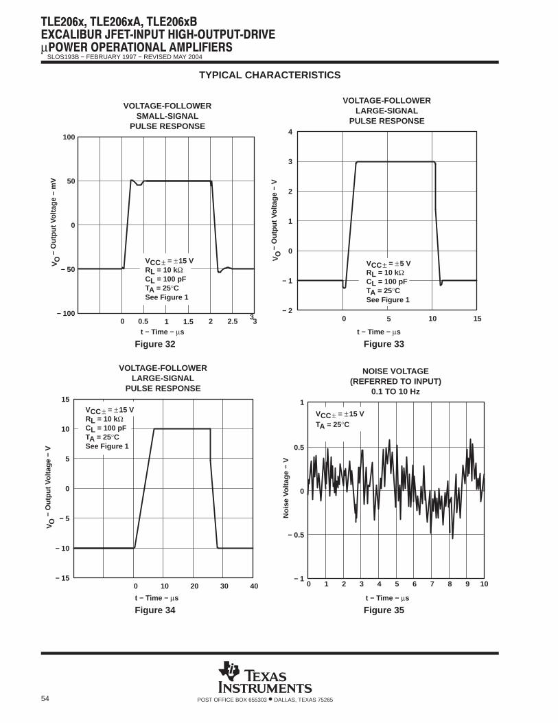
µ
SLOS193B − FEBRUARY 1997 − REVISED MAY 2004
54 POST OFFICE BOX 655303 • DALLAS, TEXAS 75265
TYPICAL CHARACTERISTICS
Figure 32
3
− O
utpu
t Vol
tage
− m
VV
O
VOLTAGE-FOLLOWERSMALL-SIGNAL
PULSE RESPONSE100
50
0
− 50
− 1000 1 2 3
t − Time − µs
VCC± = ±15 VRL = 10 kΩCL = 100 pFTA = 25°CSee Figure 1
2.51.50.5
Figure 33
VOLTAGE-FOLLOWERLARGE-SIGNAL
PULSE RESPONSE
0 5 10 15
t − Time − µs
− 2
− 1
0
1
2
3
4
− O
utpu
t Vol
tage
− V
VO
ÎÎÎÎÎÎÎÎÎÎÎÎÎÎÎÎÎÎÎÎ
VCC± = ±5 VRL = 10 kΩCL = 100 pFTA = 25°CSee Figure 1
Figure 34
− O
utpu
t Vol
tage
− V
VO
VOLTAGE-FOLLOWERLARGE-SIGNAL
PULSE RESPONSE
t − Time − µs
403020100− 15
− 10
− 5
0
5
10
15VCC± = ±15 VRL = 10 kΩCL = 100 pFTA = 25°CSee Figure 1
Figure 35
NOISE VOLTAGE(REFERRED TO INPUT)
0.1 TO 10 Hz
t − Time − µs
Noi
se V
olta
ge −
V
109876543210− 1
− 0.5
0
0.5
1
TA = 25°CVCC± = ±15 V

µ
SLOS193B − FEBRUARY 1997 − REVISED MAY 2004
55POST OFFICE BOX 655303 • DALLAS, TEXAS 75265
TYPICAL CHARACTERISTICS
Figure 36
− E
quiv
alen
t Inp
ut N
oise
Vol
tage
−V
n
EQUIVALENT INPUT NOISE VOLTAGEvs
FREQUENCY
10 k1 k100101
f − Frequency − Hz
0
20
40
60
80
100
nV/
Hz
ÎÎÎÎÎÎÎÎÎÎÎÎÎÎÎ
VCC± = ±5 VRS = 20ΩTA = 25°CSee Figure 2
Figure 37
TOTAL HARMONIC DISTORTIONvs
FREQUENCY
VCC± = ±5 V
AVD = 2VO(PP) = 2 VTA = 25°C
Source Signal
0.2
0.1
100 k10 k1 k10010
f − Frequency − Hz
TH
D −
Tot
al H
arm
onic
Dis
tort
ion
− %
0
0.3
Figure 38
TOTAL HARMONIC DISTORATIONvs
FREQUENCY
VCC± = ±5 V
Source Signal
TA = 25°CVO(PP) = 2 VAVD = 10
0.3
0.1
0.5
0.6
0
TH
D −
Tot
al H
arm
onic
Dis
tort
ion
− %
f − Frequency − Hz
10 100 1 k 10 k 100 k
0.2
0.4
Figure 39
UNITY-GAIN BANDWIDTHvs
SUPPLY VOLTAGE
See Figure 3TA = 25°CCL = 100 pFRL = 10 kΩ
2018161412108642
| VCC± | − Supply Voltage − V
2.5
2
1.5
10
− U
nity
-Gai
n B
andw
idth
− M
Hz
B1
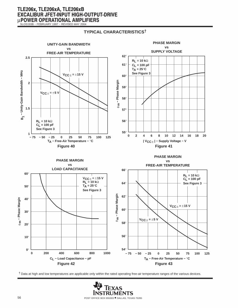
µ
SLOS193B − FEBRUARY 1997 − REVISED MAY 2004
56 POST OFFICE BOX 655303 • DALLAS, TEXAS 75265
TYPICAL CHARACTERISTICS †
Figure 40
UNITY-GAIN BANDWIDTHvs
FREE-AIR TEMPERATURE
RL = 10 kΩCL = 100 pFSee Figure 3
VCC± = ±5 V
VCC± = ±15 V
TA − Free-Air Temperature − °C1251007550250− 25− 50− 75
1
1.5
2
2.5
− U
nity
-Gai
n B
andw
idth
− M
Hz
B1
Figure 41
PHASE MARGINvs
SUPPLY VOLTAGE
RL = 10 kΩCL = 100 pFTA = 25°CSee Figure 3
62°
61°
60°
59°
58°
57°
56°
0
| VCC± | − Supply Voltage − V
2 4 6 8 10 12 14 16 18 2055°
− P
hase
Mar
gin
ÁÁÁÁ
mφ
Figure 42
PHASE MARGINvs
LOAD CAPACITANCE
CL − Load Capacitance − pF
10008006004002000
10°
20°
30°
40°
50°
0°
60°
See Figure 3TA = 25°CRL = 10 kΩVCC± = ±15 V
− P
hase
Mar
gin
ÁÁÁÁ
mφ
Figure 43
PHASE MARGINvs
FREE-AIR TEMPERATURE
− P
hase
Mar
gin
ÁÁÁÁ
mφ
1251007550250− 25− 50− 75
TA − Free-Air Temperature − °C
54°
56°
58°
60°
62°
64°
66°
VCC± = ±5 V
VCC± = ±15 V
See Figure 3CL = 100 pFRL = 10 kΩ
† Data at high and low temperatures are applicable only within the rated operating free-air temperature ranges of the various devices.

µ
SLOS193B − FEBRUARY 1997 − REVISED MAY 2004
57POST OFFICE BOX 655303 • DALLAS, TEXAS 75265
APPLICATION INFORMATION
input characteristics
The TLE206x, TLE206xA, and TLE206xB are specified with a minimum and a maximum input voltage that ifexceeded at either input could cause the device to malfunction. Because of the extremely high input impedanceand resulting low bias current requirements, the TLE206x, TLE206xA, and TLE206xB are well suited forlow-level signal processing. However, leakage currents on printed-circuit boards and sockets can easily exceedbias current requirements and cause degradation in system performance. It is good practice to include guardrings around inputs (see Figure 44). These guards should be driven from a low-impedance source at the samevoltage level as the common-mode input.
VI
R2R1
VI
R4
+
−
VO
R3
VI
+
−
VOVO
+
−
R3R4
R2R1
Where
Figure 44. Use of Guard Rings
TLE2061 input offset voltage nulling
The TLE2061 series offers external null pins that can be used to further reduce the input offset voltage. Thecircuit of Figure 45 can be connected as shown if the feature is desired. When external nulling is not needed,the null pins may be left unconnected.
+
−
VCC−
N2
N1100 kΩ
5 kΩ
IN−
IN+
OUT
Figure 45. Input Offset Voltage Nulling

µ
SLOS193B − FEBRUARY 1997 − REVISED MAY 2004
58 POST OFFICE BOX 655303 • DALLAS, TEXAS 75265
APPLICATION INFORMATION
macromodel information
Macromodel information provided was derived using Microsim Parts, the model generation software usedwith Microsim PSpice. The Boyle macromodel (see Note 5) and the subcircuit in Figure 46 were generatedusing the TLE206x typical electrical and operating characteristics at 25°C. Using this information, outputsimulations of the following key parameters can be generated to a tolerance of 20% (in most cases).
Unity-gain frequency Common-mode rejection ratio Phase margin DC output resistance AC output resistance Short-circuit output current limit
Maximum positive output voltage swing Maximum negative output voltage swing Slew rate Quiescent power dissipation Input bias current Open-loop voltage amplification
NOTE 5: G. R. Boyle, B. M. Cohn, D. O. Pederson, and J. E. Solomon, “Macromodeling of Integrated Circuit Operational Amplifiers”, IEEE Journalof Solid-State Circuits, SC-9, 353 (1974).
OUT
+
−
+
−
+
−
+
−+
−
+
− +
−
+ −
.subckt TLE2062 1 2 3 4 5c1 11 12 1.457E−12c2 6 7 15.00E−12dc 5 53 dxde 54 5 dxdlp 90 91 dxdln 92 90 dxdp 4 3 dxegnd 99 0 poly (2) (3,0) (4,0) 0 .5 .5fb 7 99 poly (5) vb vc ve vlp
+ vln 0 4.357E6 −4E6 4E6 4E6 −4E6ga 6 0 11 12 188.5E−6gcm 0 6 10 99 3.352E−9iss 3 10 dc 51.00E−6hlim 90 0 vlim 1kj1 11 2 10 jxj2 12 1 10 jxr2 6 9 100.0E3
VCC+
rp
IN−2
IN+1
VCC−
rd1
11
j1 j2
10
rss iss
3
12
rd2
ve
54de
dp
vc
dc
4
C1
53
r2
6
9
egnd
vb
fb
C2
gcm ga vlim
8
5
ro1
ro2
hlim
90
dip
91
din
92
vinvip
99
7
rd1 4 11 5.305E3rd2 4 12 5.305E3r01 8 5 280r02 7 99 280rp 3 4 113.2E3rss 10 99 3.922E6vb 9 0 dc 0vc 3 53 dc 2ve 54 4 dc 2vlim 7 8 dc 0vlp 91 0 dc 50vln 0 92 dc 50
.model dx D(Is=800.0E−18)
.model jx PJF(Is=2.000E−12 Beta = 423E−6+ Vto = −1).ends
Figure 46. Boyle Macromodel and Subcircuit
PSpice and Parts are trademarks of MicroSim Corporation.

PACKAGE OPTION ADDENDUM
www.ti.com 27-Apr-2012
Addendum-Page 1
PACKAGING INFORMATION
Orderable Device Status (1) Package Type PackageDrawing
Pins Package Qty Eco Plan (2) Lead/Ball Finish
MSL Peak Temp (3) Samples
(Requires Login)
5962-9080701M2A ACTIVE LCCC FK 20 1 TBD Call TI Call TI
5962-9080701MHA ACTIVE CFP U 10 1 TBD Call TI Call TI
5962-9080701MPA ACTIVE CDIP JG 8 1 TBD Call TI Call TI
5962-9080702Q2A ACTIVE LCCC FK 20 1 TBD Call TI Call TI
5962-9080702QHA ACTIVE CFP U 10 1 TBD Call TI Call TI
5962-9080702QPA ACTIVE CDIP JG 8 1 TBD Call TI Call TI
5962-9080703QPA ACTIVE CDIP JG 8 1 TBD Call TI Call TI
5962-9080801M2A ACTIVE LCCC FK 20 1 TBD Call TI Call TI
5962-9080801MHA ACTIVE CFP U 10 1 TBD Call TI Call TI
5962-9080801MPA ACTIVE CDIP JG 8 1 TBD Call TI Call TI
5962-9080802Q2A ACTIVE LCCC FK 20 1 TBD Call TI Call TI
5962-9080802QHA ACTIVE CFP U 10 1 TBD Call TI Call TI
5962-9080802QPA ACTIVE CDIP JG 8 1 TBD Call TI Call TI
5962-9080803QPA ACTIVE CDIP JG 8 1 TBD Call TI Call TI
5962-9080901M2A ACTIVE LCCC FK 20 1 TBD Call TI Call TI
5962-9080901MCA ACTIVE CDIP J 14 1 TBD Call TI Call TI
5962-9080901MDA ACTIVE CFP W 14 1 TBD Call TI Call TI
5962-9080902M2A ACTIVE LCCC FK 20 1 TBD Call TI Call TI
5962-9080902MCA ACTIVE CDIP J 14 1 TBD Call TI Call TI
5962-9080902MDA ACTIVE CFP W 14 1 TBD Call TI Call TI
5962-9080903Q2A ACTIVE LCCC FK 20 1 TBD Call TI Call TI
5962-9080903QCA ACTIVE CDIP J 14 1 TBD Call TI Call TI
TLE2061ACD ACTIVE SOIC D 8 75 Green (RoHS& no Sb/Br)
CU NIPDAU Level-1-260C-UNLIM
TLE2061ACDG4 ACTIVE SOIC D 8 75 Green (RoHS& no Sb/Br)
CU NIPDAU Level-1-260C-UNLIM
TLE2061ACP ACTIVE PDIP P 8 50 Pb-Free (RoHS) CU NIPDAU N / A for Pkg Type
TLE2061ACPE4 ACTIVE PDIP P 8 50 Pb-Free (RoHS) CU NIPDAU N / A for Pkg Type
TLE2061AID ACTIVE SOIC D 8 75 Green (RoHS& no Sb/Br)
CU NIPDAU Level-1-260C-UNLIM
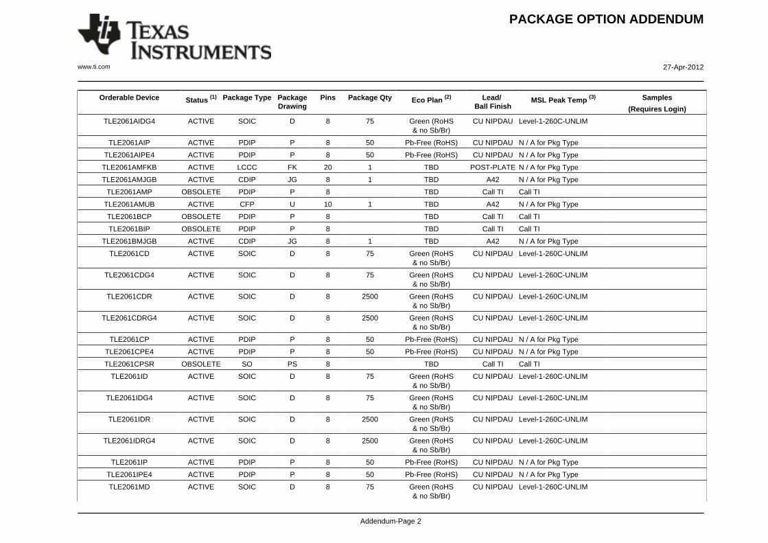
PACKAGE OPTION ADDENDUM
www.ti.com 27-Apr-2012
Addendum-Page 2
Orderable Device Status (1) Package Type PackageDrawing
Pins Package Qty Eco Plan (2) Lead/Ball Finish
MSL Peak Temp (3) Samples
(Requires Login)
TLE2061AIDG4 ACTIVE SOIC D 8 75 Green (RoHS& no Sb/Br)
CU NIPDAU Level-1-260C-UNLIM
TLE2061AIP ACTIVE PDIP P 8 50 Pb-Free (RoHS) CU NIPDAU N / A for Pkg Type
TLE2061AIPE4 ACTIVE PDIP P 8 50 Pb-Free (RoHS) CU NIPDAU N / A for Pkg Type
TLE2061AMFKB ACTIVE LCCC FK 20 1 TBD POST-PLATE N / A for Pkg Type
TLE2061AMJGB ACTIVE CDIP JG 8 1 TBD A42 N / A for Pkg Type
TLE2061AMP OBSOLETE PDIP P 8 TBD Call TI Call TI
TLE2061AMUB ACTIVE CFP U 10 1 TBD A42 N / A for Pkg Type
TLE2061BCP OBSOLETE PDIP P 8 TBD Call TI Call TI
TLE2061BIP OBSOLETE PDIP P 8 TBD Call TI Call TI
TLE2061BMJGB ACTIVE CDIP JG 8 1 TBD A42 N / A for Pkg Type
TLE2061CD ACTIVE SOIC D 8 75 Green (RoHS& no Sb/Br)
CU NIPDAU Level-1-260C-UNLIM
TLE2061CDG4 ACTIVE SOIC D 8 75 Green (RoHS& no Sb/Br)
CU NIPDAU Level-1-260C-UNLIM
TLE2061CDR ACTIVE SOIC D 8 2500 Green (RoHS& no Sb/Br)
CU NIPDAU Level-1-260C-UNLIM
TLE2061CDRG4 ACTIVE SOIC D 8 2500 Green (RoHS& no Sb/Br)
CU NIPDAU Level-1-260C-UNLIM
TLE2061CP ACTIVE PDIP P 8 50 Pb-Free (RoHS) CU NIPDAU N / A for Pkg Type
TLE2061CPE4 ACTIVE PDIP P 8 50 Pb-Free (RoHS) CU NIPDAU N / A for Pkg Type
TLE2061CPSR OBSOLETE SO PS 8 TBD Call TI Call TI
TLE2061ID ACTIVE SOIC D 8 75 Green (RoHS& no Sb/Br)
CU NIPDAU Level-1-260C-UNLIM
TLE2061IDG4 ACTIVE SOIC D 8 75 Green (RoHS& no Sb/Br)
CU NIPDAU Level-1-260C-UNLIM
TLE2061IDR ACTIVE SOIC D 8 2500 Green (RoHS& no Sb/Br)
CU NIPDAU Level-1-260C-UNLIM
TLE2061IDRG4 ACTIVE SOIC D 8 2500 Green (RoHS& no Sb/Br)
CU NIPDAU Level-1-260C-UNLIM
TLE2061IP ACTIVE PDIP P 8 50 Pb-Free (RoHS) CU NIPDAU N / A for Pkg Type
TLE2061IPE4 ACTIVE PDIP P 8 50 Pb-Free (RoHS) CU NIPDAU N / A for Pkg Type
TLE2061MD ACTIVE SOIC D 8 75 Green (RoHS& no Sb/Br)
CU NIPDAU Level-1-260C-UNLIM
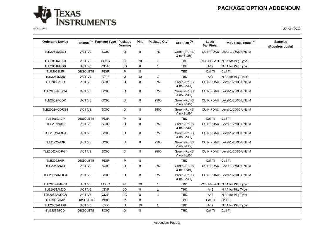
PACKAGE OPTION ADDENDUM
www.ti.com 27-Apr-2012
Addendum-Page 3
Orderable Device Status (1) Package Type PackageDrawing
Pins Package Qty Eco Plan (2) Lead/Ball Finish
MSL Peak Temp (3) Samples
(Requires Login)
TLE2061MDG4 ACTIVE SOIC D 8 75 Green (RoHS& no Sb/Br)
CU NIPDAU Level-1-260C-UNLIM
TLE2061MFKB ACTIVE LCCC FK 20 1 TBD POST-PLATE N / A for Pkg Type
TLE2061MJGB ACTIVE CDIP JG 8 1 TBD A42 N / A for Pkg Type
TLE2061MP OBSOLETE PDIP P 8 TBD Call TI Call TI
TLE2061MUB ACTIVE CFP U 10 1 TBD A42 N / A for Pkg Type
TLE2062ACD ACTIVE SOIC D 8 75 Green (RoHS& no Sb/Br)
CU NIPDAU Level-1-260C-UNLIM
TLE2062ACDG4 ACTIVE SOIC D 8 75 Green (RoHS& no Sb/Br)
CU NIPDAU Level-1-260C-UNLIM
TLE2062ACDR ACTIVE SOIC D 8 2500 Green (RoHS& no Sb/Br)
CU NIPDAU Level-1-260C-UNLIM
TLE2062ACDRG4 ACTIVE SOIC D 8 2500 Green (RoHS& no Sb/Br)
CU NIPDAU Level-1-260C-UNLIM
TLE2062ACP OBSOLETE PDIP P 8 TBD Call TI Call TI
TLE2062AID ACTIVE SOIC D 8 75 Green (RoHS& no Sb/Br)
CU NIPDAU Level-1-260C-UNLIM
TLE2062AIDG4 ACTIVE SOIC D 8 75 Green (RoHS& no Sb/Br)
CU NIPDAU Level-1-260C-UNLIM
TLE2062AIDR ACTIVE SOIC D 8 2500 Green (RoHS& no Sb/Br)
CU NIPDAU Level-1-260C-UNLIM
TLE2062AIDRG4 ACTIVE SOIC D 8 2500 Green (RoHS& no Sb/Br)
CU NIPDAU Level-1-260C-UNLIM
TLE2062AIP OBSOLETE PDIP P 8 TBD Call TI Call TI
TLE2062AMD ACTIVE SOIC D 8 75 Green (RoHS& no Sb/Br)
CU NIPDAU Level-1-260C-UNLIM
TLE2062AMDG4 ACTIVE SOIC D 8 75 Green (RoHS& no Sb/Br)
CU NIPDAU Level-1-260C-UNLIM
TLE2062AMFKB ACTIVE LCCC FK 20 1 TBD POST-PLATE N / A for Pkg Type
TLE2062AMJG ACTIVE CDIP JG 8 1 TBD A42 N / A for Pkg Type
TLE2062AMJGB ACTIVE CDIP JG 8 1 TBD A42 N / A for Pkg Type
TLE2062AMP OBSOLETE PDIP P 8 TBD Call TI Call TI
TLE2062AMUB ACTIVE CFP U 10 1 TBD A42 N / A for Pkg Type
TLE2062BCD OBSOLETE SOIC D 8 TBD Call TI Call TI

PACKAGE OPTION ADDENDUM
www.ti.com 27-Apr-2012
Addendum-Page 4
Orderable Device Status (1) Package Type PackageDrawing
Pins Package Qty Eco Plan (2) Lead/Ball Finish
MSL Peak Temp (3) Samples
(Requires Login)
TLE2062BCDR OBSOLETE SOIC D 8 TBD Call TI Call TI
TLE2062BCP OBSOLETE PDIP P 8 TBD Call TI Call TI
TLE2062BIP OBSOLETE PDIP P 8 TBD Call TI Call TI
TLE2062BMFKB OBSOLETE LCCC FK 20 TBD Call TI Call TI
TLE2062BMJG ACTIVE CDIP JG 8 1 TBD A42 N / A for Pkg Type
TLE2062BMJGB ACTIVE CDIP JG 8 1 TBD A42 N / A for Pkg Type
TLE2062CD ACTIVE SOIC D 8 75 Green (RoHS& no Sb/Br)
CU NIPDAU Level-1-260C-UNLIM
TLE2062CDG4 ACTIVE SOIC D 8 75 Green (RoHS& no Sb/Br)
CU NIPDAU Level-1-260C-UNLIM
TLE2062CDR ACTIVE SOIC D 8 2500 Green (RoHS& no Sb/Br)
CU NIPDAU Level-1-260C-UNLIM
TLE2062CDRG4 ACTIVE SOIC D 8 2500 Green (RoHS& no Sb/Br)
CU NIPDAU Level-1-260C-UNLIM
TLE2062CP ACTIVE PDIP P 8 50 Pb-Free (RoHS) CU NIPDAU N / A for Pkg Type
TLE2062CPE4 ACTIVE PDIP P 8 50 Pb-Free (RoHS) CU NIPDAU N / A for Pkg Type
TLE2062CPSR OBSOLETE SO PS 8 TBD Call TI Call TI
TLE2062ID ACTIVE SOIC D 8 75 Green (RoHS& no Sb/Br)
CU NIPDAU Level-1-260C-UNLIM
TLE2062IDG4 ACTIVE SOIC D 8 75 Green (RoHS& no Sb/Br)
CU NIPDAU Level-1-260C-UNLIM
TLE2062IDR ACTIVE SOIC D 8 2500 Green (RoHS& no Sb/Br)
CU NIPDAU Level-1-260C-UNLIM
TLE2062IDRG4 ACTIVE SOIC D 8 2500 Green (RoHS& no Sb/Br)
CU NIPDAU Level-1-260C-UNLIM
TLE2062IP ACTIVE PDIP P 8 50 Pb-Free (RoHS) CU NIPDAU N / A for Pkg Type
TLE2062IPE4 ACTIVE PDIP P 8 50 Pb-Free (RoHS) CU NIPDAU N / A for Pkg Type
TLE2062MD ACTIVE SOIC D 8 75 Green (RoHS& no Sb/Br)
CU NIPDAU Level-1-260C-UNLIM
TLE2062MDG4 ACTIVE SOIC D 8 75 Green (RoHS& no Sb/Br)
CU NIPDAU Level-1-260C-UNLIM
TLE2062MFKB ACTIVE LCCC FK 20 1 TBD POST-PLATE N / A for Pkg Type
TLE2062MJG ACTIVE CDIP JG 8 1 TBD A42 N / A for Pkg Type
TLE2062MJGB ACTIVE CDIP JG 8 1 TBD A42 N / A for Pkg Type
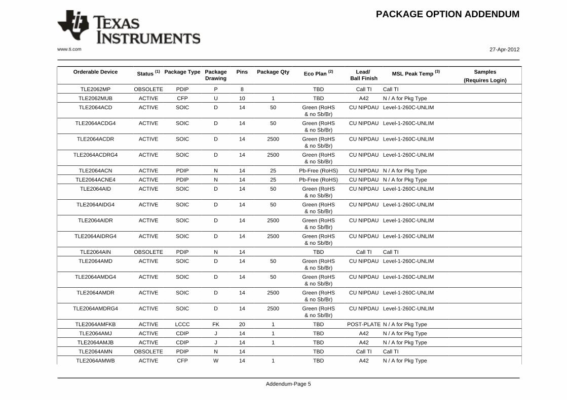
PACKAGE OPTION ADDENDUM
www.ti.com 27-Apr-2012
Addendum-Page 5
Orderable Device Status (1) Package Type PackageDrawing
Pins Package Qty Eco Plan (2) Lead/Ball Finish
MSL Peak Temp (3) Samples
(Requires Login)
TLE2062MP OBSOLETE PDIP P 8 TBD Call TI Call TI
TLE2062MUB ACTIVE CFP U 10 1 TBD A42 N / A for Pkg Type
TLE2064ACD ACTIVE SOIC D 14 50 Green (RoHS& no Sb/Br)
CU NIPDAU Level-1-260C-UNLIM
TLE2064ACDG4 ACTIVE SOIC D 14 50 Green (RoHS& no Sb/Br)
CU NIPDAU Level-1-260C-UNLIM
TLE2064ACDR ACTIVE SOIC D 14 2500 Green (RoHS& no Sb/Br)
CU NIPDAU Level-1-260C-UNLIM
TLE2064ACDRG4 ACTIVE SOIC D 14 2500 Green (RoHS& no Sb/Br)
CU NIPDAU Level-1-260C-UNLIM
TLE2064ACN ACTIVE PDIP N 14 25 Pb-Free (RoHS) CU NIPDAU N / A for Pkg Type
TLE2064ACNE4 ACTIVE PDIP N 14 25 Pb-Free (RoHS) CU NIPDAU N / A for Pkg Type
TLE2064AID ACTIVE SOIC D 14 50 Green (RoHS& no Sb/Br)
CU NIPDAU Level-1-260C-UNLIM
TLE2064AIDG4 ACTIVE SOIC D 14 50 Green (RoHS& no Sb/Br)
CU NIPDAU Level-1-260C-UNLIM
TLE2064AIDR ACTIVE SOIC D 14 2500 Green (RoHS& no Sb/Br)
CU NIPDAU Level-1-260C-UNLIM
TLE2064AIDRG4 ACTIVE SOIC D 14 2500 Green (RoHS& no Sb/Br)
CU NIPDAU Level-1-260C-UNLIM
TLE2064AIN OBSOLETE PDIP N 14 TBD Call TI Call TI
TLE2064AMD ACTIVE SOIC D 14 50 Green (RoHS& no Sb/Br)
CU NIPDAU Level-1-260C-UNLIM
TLE2064AMDG4 ACTIVE SOIC D 14 50 Green (RoHS& no Sb/Br)
CU NIPDAU Level-1-260C-UNLIM
TLE2064AMDR ACTIVE SOIC D 14 2500 Green (RoHS& no Sb/Br)
CU NIPDAU Level-1-260C-UNLIM
TLE2064AMDRG4 ACTIVE SOIC D 14 2500 Green (RoHS& no Sb/Br)
CU NIPDAU Level-1-260C-UNLIM
TLE2064AMFKB ACTIVE LCCC FK 20 1 TBD POST-PLATE N / A for Pkg Type
TLE2064AMJ ACTIVE CDIP J 14 1 TBD A42 N / A for Pkg Type
TLE2064AMJB ACTIVE CDIP J 14 1 TBD A42 N / A for Pkg Type
TLE2064AMN OBSOLETE PDIP N 14 TBD Call TI Call TI
TLE2064AMWB ACTIVE CFP W 14 1 TBD A42 N / A for Pkg Type

PACKAGE OPTION ADDENDUM
www.ti.com 27-Apr-2012
Addendum-Page 6
Orderable Device Status (1) Package Type PackageDrawing
Pins Package Qty Eco Plan (2) Lead/Ball Finish
MSL Peak Temp (3) Samples
(Requires Login)
TLE2064BCN OBSOLETE PDIP N 14 TBD Call TI Call TI
TLE2064BIN OBSOLETE PDIP N 14 TBD Call TI Call TI
TLE2064BMFKB ACTIVE LCCC FK 20 1 TBD POST-PLATE N / A for Pkg Type
TLE2064BMJ ACTIVE CDIP J 14 1 TBD A42 N / A for Pkg Type
TLE2064BMJB ACTIVE CDIP J 14 1 TBD A42 N / A for Pkg Type
TLE2064BMN OBSOLETE PDIP N 14 TBD Call TI Call TI
TLE2064CD ACTIVE SOIC D 14 50 Green (RoHS& no Sb/Br)
CU NIPDAU Level-1-260C-UNLIM
TLE2064CDG4 ACTIVE SOIC D 14 50 Green (RoHS& no Sb/Br)
CU NIPDAU Level-1-260C-UNLIM
TLE2064CDR ACTIVE SOIC D 14 2500 Green (RoHS& no Sb/Br)
CU NIPDAU Level-1-260C-UNLIM
TLE2064CDRG4 ACTIVE SOIC D 14 2500 Green (RoHS& no Sb/Br)
CU NIPDAU Level-1-260C-UNLIM
TLE2064CN ACTIVE PDIP N 14 25 Pb-Free (RoHS) CU NIPDAU N / A for Pkg Type
TLE2064CNE4 ACTIVE PDIP N 14 25 Pb-Free (RoHS) CU NIPDAU N / A for Pkg Type
TLE2064CNSR OBSOLETE SO NS 14 TBD Call TI Call TI
TLE2064ID ACTIVE SOIC D 14 50 Green (RoHS& no Sb/Br)
CU NIPDAU Level-1-260C-UNLIM
TLE2064IDG4 ACTIVE SOIC D 14 50 Green (RoHS& no Sb/Br)
CU NIPDAU Level-1-260C-UNLIM
TLE2064IDR ACTIVE SOIC D 14 2500 Green (RoHS& no Sb/Br)
CU NIPDAU Level-1-260C-UNLIM
TLE2064IDRG4 ACTIVE SOIC D 14 2500 Green (RoHS& no Sb/Br)
CU NIPDAU Level-1-260C-UNLIM
TLE2064IN ACTIVE PDIP N 14 25 Pb-Free (RoHS) CU NIPDAU N / A for Pkg Type
TLE2064INE4 ACTIVE PDIP N 14 25 Pb-Free (RoHS) CU NIPDAU N / A for Pkg Type
TLE2064MD ACTIVE SOIC D 14 50 Green (RoHS& no Sb/Br)
CU NIPDAU Level-1-260C-UNLIM
TLE2064MDG4 ACTIVE SOIC D 14 50 Green (RoHS& no Sb/Br)
CU NIPDAU Level-1-260C-UNLIM
TLE2064MDR ACTIVE SOIC D 14 1 Green (RoHS& no Sb/Br)
CU NIPDAU Level-1-260C-UNLIM

PACKAGE OPTION ADDENDUM
www.ti.com 27-Apr-2012
Addendum-Page 7
Orderable Device Status (1) Package Type PackageDrawing
Pins Package Qty Eco Plan (2) Lead/Ball Finish
MSL Peak Temp (3) Samples
(Requires Login)
TLE2064MDRG4 ACTIVE SOIC D 14 2500 Green (RoHS& no Sb/Br)
CU NIPDAU Level-1-260C-UNLIM
TLE2064MFKB ACTIVE LCCC FK 20 1 TBD POST-PLATE N / A for Pkg Type
TLE2064MJ ACTIVE CDIP J 14 1 TBD A42 N / A for Pkg Type
TLE2064MJB ACTIVE CDIP J 14 1 TBD A42 N / A for Pkg Type
TLE2064MN OBSOLETE PDIP N 14 TBD Call TI Call TI
TLE2064MWB ACTIVE CFP W 14 1 TBD A42 N / A for Pkg Type (1) The marketing status values are defined as follows:ACTIVE: Product device recommended for new designs.LIFEBUY: TI has announced that the device will be discontinued, and a lifetime-buy period is in effect.NRND: Not recommended for new designs. Device is in production to support existing customers, but TI does not recommend using this part in a new design.PREVIEW: Device has been announced but is not in production. Samples may or may not be available.OBSOLETE: TI has discontinued the production of the device.
(2) Eco Plan - The planned eco-friendly classification: Pb-Free (RoHS), Pb-Free (RoHS Exempt), or Green (RoHS & no Sb/Br) - please check http://www.ti.com/productcontent for the latest availabilityinformation and additional product content details.TBD: The Pb-Free/Green conversion plan has not been defined.Pb-Free (RoHS): TI's terms "Lead-Free" or "Pb-Free" mean semiconductor products that are compatible with the current RoHS requirements for all 6 substances, including the requirement thatlead not exceed 0.1% by weight in homogeneous materials. Where designed to be soldered at high temperatures, TI Pb-Free products are suitable for use in specified lead-free processes.Pb-Free (RoHS Exempt): This component has a RoHS exemption for either 1) lead-based flip-chip solder bumps used between the die and package, or 2) lead-based die adhesive used betweenthe die and leadframe. The component is otherwise considered Pb-Free (RoHS compatible) as defined above.Green (RoHS & no Sb/Br): TI defines "Green" to mean Pb-Free (RoHS compatible), and free of Bromine (Br) and Antimony (Sb) based flame retardants (Br or Sb do not exceed 0.1% by weightin homogeneous material)
(3) MSL, Peak Temp. -- The Moisture Sensitivity Level rating according to the JEDEC industry standard classifications, and peak solder temperature.
Important Information and Disclaimer:The information provided on this page represents TI's knowledge and belief as of the date that it is provided. TI bases its knowledge and belief on informationprovided by third parties, and makes no representation or warranty as to the accuracy of such information. Efforts are underway to better integrate information from third parties. TI has taken andcontinues to take reasonable steps to provide representative and accurate information but may not have conducted destructive testing or chemical analysis on incoming materials and chemicals.TI and TI suppliers consider certain information to be proprietary, and thus CAS numbers and other limited information may not be available for release.
In no event shall TI's liability arising out of such information exceed the total purchase price of the TI part(s) at issue in this document sold by TI to Customer on an annual basis.
OTHER QUALIFIED VERSIONS OF TLE2061, TLE2061A, TLE2061AM, TLE2061B, TLE2061BM, TLE2061M, TLE2062, TLE2062A, TLE2062AM, TLE2062B,TLE2062BM, TLE2062M, TLE2064, TLE2064A, TLE2064AM, TLE2064B, TLE2064BM, TLE2064M :
• Catalog: TLE2061A, TLE2061B, TLE2061, TLE2062A, TLE2062B, TLE2062, TLE2064A, TLE2064B, TLE2064

PACKAGE OPTION ADDENDUM
www.ti.com 27-Apr-2012
Addendum-Page 8
• Military: TLE2061M, TLE2061AM, TLE2061BM, TLE2062M, TLE2062AM, TLE2062BM, TLE2064M, TLE2064AM, TLE2064BM
NOTE: Qualified Version Definitions:
• Catalog - TI's standard catalog product
• Military - QML certified for Military and Defense Applications

TAPE AND REEL INFORMATION
*All dimensions are nominal
Device PackageType
PackageDrawing
Pins SPQ ReelDiameter
(mm)
ReelWidth
W1 (mm)
A0(mm)
B0(mm)
K0(mm)
P1(mm)
W(mm)
Pin1Quadrant
TLE2061CDR SOIC D 8 2500 330.0 12.4 6.4 5.2 2.1 8.0 12.0 Q1
TLE2061IDR SOIC D 8 2500 330.0 12.4 6.4 5.2 2.1 8.0 12.0 Q1
TLE2062ACDR SOIC D 8 2500 330.0 12.4 6.4 5.2 2.1 8.0 12.0 Q1
TLE2062AIDR SOIC D 8 2500 330.0 12.4 6.4 5.2 2.1 8.0 12.0 Q1
TLE2062CDR SOIC D 8 2500 330.0 12.4 6.4 5.2 2.1 8.0 12.0 Q1
TLE2062IDR SOIC D 8 2500 330.0 12.4 6.4 5.2 2.1 8.0 12.0 Q1
TLE2064ACDR SOIC D 14 2500 330.0 16.4 6.5 9.0 2.1 8.0 16.0 Q1
TLE2064AIDR SOIC D 14 2500 330.0 16.4 6.5 9.0 2.1 8.0 16.0 Q1
TLE2064AMDR SOIC D 14 2500 330.0 16.4 6.5 9.0 2.1 8.0 16.0 Q1
TLE2064CDR SOIC D 14 2500 330.0 16.4 6.5 9.0 2.1 8.0 16.0 Q1
TLE2064IDR SOIC D 14 2500 330.0 16.4 6.5 9.0 2.1 8.0 16.0 Q1
TLE2064MDR SOIC D 14 1 330.0 16.4 6.5 9.0 2.1 8.0 16.0 Q1
PACKAGE MATERIALS INFORMATION
www.ti.com 14-Jul-2012
Pack Materials-Page 1

*All dimensions are nominal
Device Package Type Package Drawing Pins SPQ Length (mm) Width (mm) Height (mm)
TLE2061CDR SOIC D 8 2500 340.5 338.1 20.6
TLE2061IDR SOIC D 8 2500 340.5 338.1 20.6
TLE2062ACDR SOIC D 8 2500 340.5 338.1 20.6
TLE2062AIDR SOIC D 8 2500 340.5 338.1 20.6
TLE2062CDR SOIC D 8 2500 340.5 338.1 20.6
TLE2062IDR SOIC D 8 2500 340.5 338.1 20.6
TLE2064ACDR SOIC D 14 2500 367.0 367.0 38.0
TLE2064AIDR SOIC D 14 2500 367.0 367.0 38.0
TLE2064AMDR SOIC D 14 2500 367.0 367.0 38.0
TLE2064CDR SOIC D 14 2500 367.0 367.0 38.0
TLE2064IDR SOIC D 14 2500 367.0 367.0 38.0
TLE2064MDR SOIC D 14 1 367.0 367.0 38.0
PACKAGE MATERIALS INFORMATION
www.ti.com 14-Jul-2012
Pack Materials-Page 2
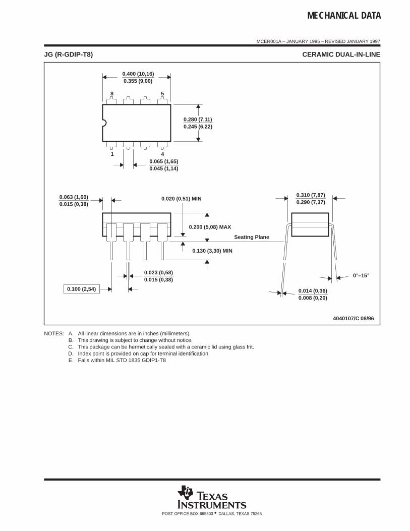
MECHANICAL DATA
MCER001A – JANUARY 1995 – REVISED JANUARY 1997
POST OFFICE BOX 655303 • DALLAS, TEXAS 75265
JG (R-GDIP-T8) CERAMIC DUAL-IN-LINE
0.310 (7,87)0.290 (7,37)
0.014 (0,36)0.008 (0,20)
Seating Plane
4040107/C 08/96
5
40.065 (1,65)0.045 (1,14)
8
1
0.020 (0,51) MIN
0.400 (10,16)0.355 (9,00)
0.015 (0,38)0.023 (0,58)
0.063 (1,60)0.015 (0,38)
0.200 (5,08) MAX
0.130 (3,30) MIN
0.245 (6,22)0.280 (7,11)
0.100 (2,54)
0°–15°
NOTES: A. All linear dimensions are in inches (millimeters).B. This drawing is subject to change without notice.C. This package can be hermetically sealed with a ceramic lid using glass frit.D. Index point is provided on cap for terminal identification.E. Falls within MIL STD 1835 GDIP1-T8
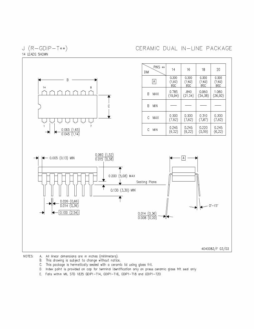
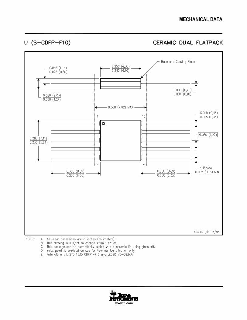


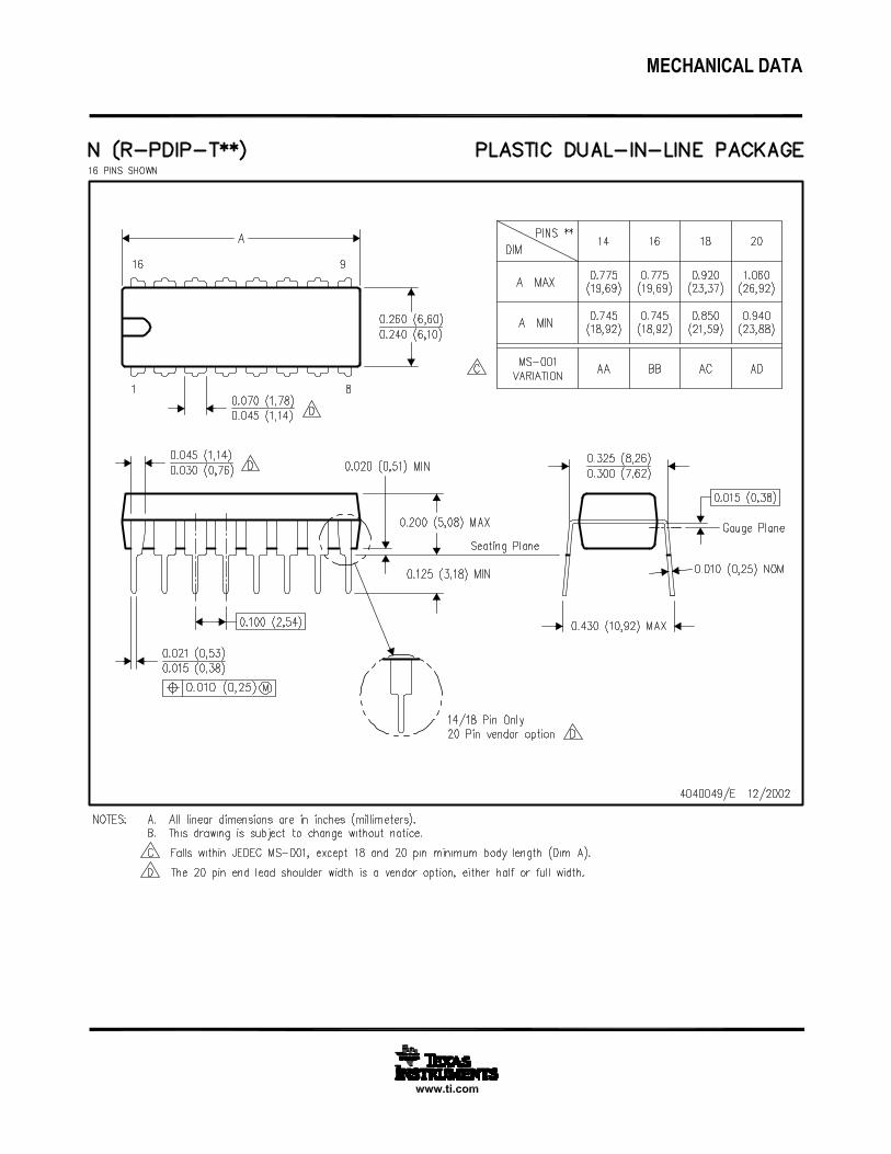


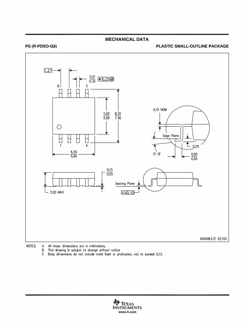

IMPORTANT NOTICE
Texas Instruments Incorporated and its subsidiaries (TI) reserve the right to make corrections, enhancements, improvements and otherchanges to its semiconductor products and services per JESD46, latest issue, and to discontinue any product or service per JESD48, latestissue. Buyers should obtain the latest relevant information before placing orders and should verify that such information is current andcomplete. All semiconductor products (also referred to herein as “components”) are sold subject to TI’s terms and conditions of salesupplied at the time of order acknowledgment.
TI warrants performance of its components to the specifications applicable at the time of sale, in accordance with the warranty in TI’s termsand conditions of sale of semiconductor products. Testing and other quality control techniques are used to the extent TI deems necessaryto support this warranty. Except where mandated by applicable law, testing of all parameters of each component is not necessarilyperformed.
TI assumes no liability for applications assistance or the design of Buyers’ products. Buyers are responsible for their products andapplications using TI components. To minimize the risks associated with Buyers’ products and applications, Buyers should provideadequate design and operating safeguards.
TI does not warrant or represent that any license, either express or implied, is granted under any patent right, copyright, mask work right, orother intellectual property right relating to any combination, machine, or process in which TI components or services are used. Informationpublished by TI regarding third-party products or services does not constitute a license to use such products or services or a warranty orendorsement thereof. Use of such information may require a license from a third party under the patents or other intellectual property of thethird party, or a license from TI under the patents or other intellectual property of TI.
Reproduction of significant portions of TI information in TI data books or data sheets is permissible only if reproduction is without alterationand is accompanied by all associated warranties, conditions, limitations, and notices. TI is not responsible or liable for such altereddocumentation. Information of third parties may be subject to additional restrictions.
Resale of TI components or services with statements different from or beyond the parameters stated by TI for that component or servicevoids all express and any implied warranties for the associated TI component or service and is an unfair and deceptive business practice.TI is not responsible or liable for any such statements.
Buyer acknowledges and agrees that it is solely responsible for compliance with all legal, regulatory and safety-related requirementsconcerning its products, and any use of TI components in its applications, notwithstanding any applications-related information or supportthat may be provided by TI. Buyer represents and agrees that it has all the necessary expertise to create and implement safeguards whichanticipate dangerous consequences of failures, monitor failures and their consequences, lessen the likelihood of failures that might causeharm and take appropriate remedial actions. Buyer will fully indemnify TI and its representatives against any damages arising out of the useof any TI components in safety-critical applications.
In some cases, TI components may be promoted specifically to facilitate safety-related applications. With such components, TI’s goal is tohelp enable customers to design and create their own end-product solutions that meet applicable functional safety standards andrequirements. Nonetheless, such components are subject to these terms.
No TI components are authorized for use in FDA Class III (or similar life-critical medical equipment) unless authorized officers of the partieshave executed a special agreement specifically governing such use.
Only those TI components which TI has specifically designated as military grade or “enhanced plastic” are designed and intended for use inmilitary/aerospace applications or environments. Buyer acknowledges and agrees that any military or aerospace use of TI componentswhich have not been so designated is solely at the Buyer's risk, and that Buyer is solely responsible for compliance with all legal andregulatory requirements in connection with such use.
TI has specifically designated certain components which meet ISO/TS16949 requirements, mainly for automotive use. Components whichhave not been so designated are neither designed nor intended for automotive use; and TI will not be responsible for any failure of suchcomponents to meet such requirements.
Products Applications
Audio www.ti.com/audio Automotive and Transportation www.ti.com/automotive
Amplifiers amplifier.ti.com Communications and Telecom www.ti.com/communications
Data Converters dataconverter.ti.com Computers and Peripherals www.ti.com/computers
DLP® Products www.dlp.com Consumer Electronics www.ti.com/consumer-apps
DSP dsp.ti.com Energy and Lighting www.ti.com/energy
Clocks and Timers www.ti.com/clocks Industrial www.ti.com/industrial
Interface interface.ti.com Medical www.ti.com/medical
Logic logic.ti.com Security www.ti.com/security
Power Mgmt power.ti.com Space, Avionics and Defense www.ti.com/space-avionics-defense
Microcontrollers microcontroller.ti.com Video and Imaging www.ti.com/video
RFID www.ti-rfid.com
OMAP Applications Processors www.ti.com/omap TI E2E Community e2e.ti.com
Wireless Connectivity www.ti.com/wirelessconnectivity
Mailing Address: Texas Instruments, Post Office Box 655303, Dallas, Texas 75265Copyright © 2012, Texas Instruments Incorporated