© copr. 1949-1998 hewlett-packard co. · a programmable selective level meter (wave analyzer) with...
TRANSCRIPT

© Copr. 1949-1998 Hewlett-Packard Co.

H E W L E T T - P A C K A R D J O U R N A L Technica l In format ion f rom the Laborator ies o f Hewlet t -Packard Company
MAY 1980 Volume 31 • Number 5
Contents:
A Programmable Select ive Level Meter (Wave Analyzer) with Synthesized Tuning, Auto- r a n g i n g , a n d A u t o m a t i c C a l i b r a t i o n , b y P a u l L T h o m a s I t ' s u s e f u l i n a u d i o , s o n a r ,
rad io , and f requency d iv is ion mul t ip lex systems tes t ing.
Prec is ion Synthes izer /Leve l Genera tor Has H igh Spect ra l Pur i ty fo r Te lecommunica t i ons Tes t ing , by Ph i l l i p D . Wins low A power fu l complement to a se lec t i ve leve l mete r , i t ' s
a lso a prec is ion genera l -purpose s igna l source.
A M o n o l i t h i c T h e r m a l C o n v e r t e r , b y P e t e r M . O ' N e i l l I n t e g r a t e d c i r c u i t t e c h n o l o g y p r o duces a conver ter . broadband, monol i th ic s i l icon thermal rms- to-dc conver ter .
Increased Versat i l i ty for a Versat i le Log ic Sta te Analyzer , by Just in S. Morr i l l , J r . and John D. Hansen Now i t can capture microprocessor events a t d i f fe rent t imes and p laces and d is
p lay them a l l together .
G e n e r a l - P u r p o s e M o d u l e A d a p t s D e d i c a t e d L o g i c S t a t e A n a l y z e r t o A l m o s t A n y Microprocessor , by Deborah J . Ogden Persona l i ty modules customize th is ana lyzer fo r tes t
ing par t icu lar microprocessors . Th is new module isn ' t so par t icu lar .
In this Issue: Our cover photo shows two of th is month 's featured products doing one of their pr incipal
jobs, test ing te lephone equipment . A f requency d iv is ion mul t ip lex (FDM) te lephone system like the range on the cover carries many telephone channels, each spanning a frequency range of 0 to composite Hz, stacked one on top of another in frequency. Thus the composite signal trans mitted energy point to point over microwave radio l inks is a broadband signal with i ts energy
' I spread out over a wide range of frequencies. In testing a system l ike this, i t 's often necessary " "a to channel. how much energy is in one part icular channel or part of a channel. That 's the job
i ) o f a t h e l e v e l m e t e r l i k e M o d e l 3 5 8 6 A / B / C ( p a g e 3 ) . I t s e l e c t s t h e n a r r o w b a n d o f f r e quencies narrow user wants to measure, and then itmefers the signal level (the amount of energy) in that narrow band. Somet imes i t ' s use fu l to send a p rec ise tone over a channe l and measure what happens to i t w i th a se lec t i ve l eve l me te r . Gene ra t i ng t ha t t one w i t h a p rec i se f r equency and magn i t ude i s t he j ob o f Mode l 3336A/B/C Synthesizer/Level Generator (page 9). The A and B vers ions of the 3586A/B/C and 3336A/B/C are des igned uses for te lephone tes t ing in Europe and Nor th Amer ica. And s ince there are many o ther uses for such ins t ruments bes ides te lephone tes t ing , the re 's a C vers ion o f each one fo r genera l -purpose des ign , manufactur ing and maintenance appl icat ions. (We' re gratefu l to Southern Paci f ic Communicat ions Company for a l lowing us to use the i r FDM equipment as a backdrop for our cover photo. )
Round ing fo r th is month 's i ssue are two log ic s ta te ana lyzer a r t i c les . Log ic s ta te ana lyzers are used fo r checking informat ion f low in d ig i ta l systems such as computers and microprocessors. Model 1610A has been Hewle t t -Packard ' s mos t capab le genera l -pu rpose log ic s ta te ana lyze r . Now the re ' s a new vers ion , Mode l 161 OB, microprocessors, the more flexibility in how data is captured (page 14). For example, in some microprocessors, the addresses of memory locat ions and the data stored in those locat ions appear on the same bus, but at di f ferent t imes. s ide . 161 OB can catch them both and d isp lay them s ide by s ide.
Model 1 microprocessors. customize it Logic State Analyzer is designed specifically for testing microprocessors. You can customize it to test Several modules microprocessor by plugging in a personal i ty module. Several personal i ty modules are avai lable, one for each of the more widely used microprocessors. Unl ike these, the latest module, Option 001 , i s n ' t t h e f o r a n y p a r t i c u l a r m i c r o p r o c e s s o r , b u t i n s t e a d t u r n s t h e 1 6 1 1 A i n t o a g e n e r a l - p u r p o s e m i c r o processor analyzer . Th is s tory s tar ts on page 19.
- R . P . D o / a n
Edi tor, Richard P Dolan • Contr ibut ing Edi tor, Howard L Roberts • Art Director, Photographer. Arvid A. Danielson I l lustrator , Nancy S Vanderbloom • Administrat ive Services, Typography, Anne S. LoPrest i • European Product ion Manager, Dick Leeksma
2 H E W L E T T - P A C K A R D J O U R N A L M A Y 1 9 8 0 Â © H e w l e t t - P a c k a r d C o m p a n y 1 9 8 0 P r i n t e d i n U S A .
© Copr. 1949-1998 Hewlett-Packard Co.

A Programmable Selective Level Meter (Wave Analyzer) with Synthesized Tuning, Autoranging, and Automatic Calibration Cover ing an input f requency range of 50 Hz to 32.5 MHz, th is tuned vo l tmeter measures character is t ics o f both the vo ice channe ls and the mul t ip lexed channe ls o f FDM communicat ions systems. An al ternate version funct ions as a genera l -purpose wave ana lyzer .
b y P a u l L T h o m a s
INSTRUMENTS THAT CAN TUNE OUT all but one frequency component in a complex signal and measure the component's amplitude precisely are known as
selective level meters or wave analyzers — terms that have practically become synonymous.
If there has been any difference between a wave analyzer and a selective level meter (SLM) it is that the SLM is optimized with the appropriate bandwidths and input im pedance levels for telephone system measurements while the wave analyzer is designed for general-purpose use on all kinds of signals. The SLM is designed to select and measure a particular telephone channel or pilot tone in an FDM (frequency division multiplexed) communications
system. Spectrum analyzers, another kind of instrument, also
separate the frequency components of a signal for analysis, but since they display all components within a selected frequency range at the same time, they are designed for wide dynamic display range and therefore have more diffi culty in achieving the amplitude measurement accuracy that SLM/wave analyzers are capable of achieving. *A fundamenta l d i f fe rence between wave and spect rum ana lyzers is in the shapes o f the f i l t e r response Spec t rum ana lyze rs need f i l t e rs w i th Gauss ian -shaped response so the f i l t e r s w a v e r i n g a s t h e t u n i n g s w e e p s a s i g n a l t h r o u g h t h e f i l t e r ' s p a s s b a n d . A w a v e analyzer's f i l ters, on the other hand, can have steeper skirts since the signal usually remains in the passband long enough for transients to sett le down, and the top of the response curve s f la t tened to a l low for a s l ight amount of mistunlng.
a • n TI
i n n r i m m T ] Q s t a m m n r n
^ . ^ m r i n r i à T i
0
n = F i g . 1 . M o d e l 3 5 8 6 A / B / C S e l e c t ive Level Meter (3586C shown) is d e s i g n e d f o r g e n e r a l - p u r p o s e w a v e a n a l y s i s a n d t e l e c o m m u n i ca t ions app l ica t ions inc lud ing au d io , sona r , r ad io , and f r equency d iv is ion mul t ip lex (FDM) systems testing. It has a frequency range of 50 Hz to 32.5 MHz, ±0.2-dB level accu racy , and 0 .1 -Hz f requency resolution.
MAY 1980 HEWLETT-PACKARD JOURNAL 3
© Copr. 1949-1998 Hewlett-Packard Co.

m Q m m m m m - - * B * * ^  » m ^  » * - â € ¢ - T E R M I N A T I O N ^ â € ¢ â € ¢ â € ¢ â € ¢ ^ l ^  ·  · ^  · ^ ^ ^ l  · H
T n n n m T - r D
. • à : ÃD Q
• 9 A
Fig. differ configurations B, and C versions of the 3586 Selective Level Meter differ in their input configurations and internal f i l ters. Model 3586 A meets CCITT requirements; Model 3586B is for North American
( B e l l ) a n a l y s i s . a n d M o d e l 3 5 8 6 C i s f o r g e n e r a l - p u r p o s e w a v e a n a l y s i s .
Hewlett-Packard has been designing and manufacturing wave analyzers for years, some of which (the 312C and 312D) are optimized for telephone applications. New SLMs and wave analyzers are now being designed around mi croprocessors to achieve greatly enhanced capabilities. The first of the new microprocessor-controlled generation of SLMs was the Model 3745A Selective Level Measuring Set,1 introduced in 1975. This instrument greatly reduces the time needed to tune to a particular channel or pilot tone in an FDM system by having tables of the 3600 or so FDM frequencies stored in read-only memory (ROM). The operator tunes the instrument to the proper frequency sim ply by entering a description of the desired channel (chan nel number, group number, supergroup number, etc.) by way of the keyboard. The microprocessor looks up the cor rect frequency for the selected measurement on that chan nel and then, by control of the synthesized first local oscil lator, tunes the analyzer accordingly. This plus autoranging greatly speeds measurements of gain, loss, noise, and other characteristics of telephone systems. It also enables the instrument to be readily incorporated into automatic sys tems.
A lower-cost microprocessor-controlled SLM has now been designed for use in laboratory, production test, and system maintenance applications. This one, Model 3586A/B/C (Fig. 1), is tuned manually, but as we shall see, microprocessor control simplifies its tuning and gives it other convenience features such as full remote control through the HP interface bus (HP-IB).
An Overv iew The new Model 3586A/B/C Selective Level Meter has a
frequency range of 50 Hz to 32.5 MHz, covering both the telephone voice band and multiplexed channel frequen cies. * * The user may thus compare measurements made on the same channel at both the voice-frequency and multi plexed levels. A synthesized local oscillator makes it pos- 'Compat ib le w i th ANSI / IEEE 488-1978 * *The ins t rument i s usab le down to 10 Hz w i th unspec i f i ed per fo rmance
sible to set the frequency tuning with 0.1 -Hz resolution. A built-in counter measures the frequency of an unknown signal accurately so the instrument can be tuned exactly to that frequency without the necessity to spend time "rock ing" the tuning control to center the signal in the instru ment's passband.
The amplitude measurement range is from +25 to -125 dBm with errors less than ±0.2 dB over the major part of the instrument's input range. Autoranging permits use of a 10-dB display range, giving an amplitude measurement resolution of 0.01 dB for examining the fine-grain fre quency response of telephone channels.
The microprocessor scales the measured quantity so re sults are displayed in the units selected (dBm, dBpW, or dBV referred to 0.775V). A reference reading may be stored as an offset by use of the RDNG-»OFFSET key so relative measurements may be made, for example, with respect to the test level point (TLP) or the fundamental frequency component of a signal. Any other reference value may also be stored as an offset using the numeric keypad.
Automatic calibration to an internal standard every three minutes and use of a true-rms detector assure accuracy in both tone and noise measurements. The instrument can also measure the total power in broadband signals applied to its input, giving a quick indication of the power level of a multiplexed signal.
To meet the requirements of a broad range of applica tions, several input configurations are provided. Model 3586A, intended for use in CCITT-compatible telephone systems, has a 75O/10kfi single-ended input using a BNC connector, and 150Ã1 and 600Ã1 balanced inputs using Siemens 3-prong connectors (Fig. 2). These input config urations are suitable for connecting the instrument to vari ous levels within the FDM hierarchy.
Model 3586B, for Bell-compatible systems, has a 75ÃI single-ended input and 124Ã1, 135Ã1, and 600ÃÃ balanced inputs with appropriate WECO connectors.
Model 3586C, intended for general-purpose wave- analyzer applications, has a single-ended 50fi/75fi input
4 H E W L E T T - P A C K A R D J O U R N A L M A Y 1 9 8 0
© Copr. 1949-1998 Hewlett-Packard Co.

0-32.5 MHz Second Mixer /1 5 .625 kHz
Swi t chab le G a i n A m p l i f i e r
Tracking Output
Fig. receiver. bandwidth 3586A/B/C is a dual-conversion superheterodyne receiver. Resolution bandwidth is determined by the second-IF f i l ters .
using a BNC connector, and a 600fi balanced input using a dual-banana connector.
Other impedance-connector combinations are available for any of the versions. All provide probe power at the front panel for wideband, high-impedance, active probes.
Filter bandwidths of 20 Hz and 400 Hz are standard on all versions, and 3100 Hz is optional. Model 3586A (CCITTJ also includes a 1740-Hz psophometric equivalent noise- weighting filter, and Model 3586B (Bell) includes a 2000- Hz C-message equivalent noise-weighting filter so mea surements made with these instruments can be related to traditional noise measurements on telephone systems. The transmission impairments measurement option includes a highly selective 3100-Hz channel filter plus a true psophometric or C-message noise weighting filter for more accurate noise level measurements. With this option, the telephone-oriented versions can make transmission im pairment measurements such as noise-with-tone, signal- to-noise-with-tone ratio, phase jitter, and single-level im pulse noise. Because of their extended frequency range, the instruments are capable of making these measurements at the multiplex level as well as at voice frequencies.
All versions also work with the Model 3336A/B/C Synthesizer/Level Generator (see page 9). This instrument generates sine waves with accurately-controlled amplitude levels. Its tuning can be controlled by the 3586A/B/C SLM through the HP Interface Bus to function as a tracking signal source for measurements made with the 3586A/B/C. The 3586A/B/C SLM itself has a tracking output, useful for fre quency-response measurements but lacking the level set- tability of the 3336A/B/C.
Semiautomated Tuning To tune the 3586A/B/C, the operator enters the desired
frequency through the numeric keyboard. To change the tuning, the operator can enter a new number or use the up-down step keys or the rotary tuning knob. The amount by which the step keys and tuning knob change the fre quency can be selected with 0.1-Hz resolution by entering the desired step value through the numeric keypad and pressing the FREQ STEP key. One can enter the frequency being measured as the frequency step, for example, and then step from harmonic to harmonic, or enlei 4 kHz anu step from one channel of an FDM signal to the next.
When measurements are being made on multiplexed telephone channels, the user need only enter the carrier frequency for that channel, then indicate whether the chan
nel signal is in the upper or lower sideband, using the /I (upper) or |~\ (lower) key. The instrument's tuning is automatically offset the exact 1850 Hz needed to center the tuning in the selected sideband. Other keys can be used to offset the tuning to center the tuning on the channel test tones (800/1010 Hz for CCITT, 1004/2600 Hz for Bell). In each case it is not necessary to enter a nine-digit number to change the frequency — simply pressing the appropriate key changes the tuning by the required amount, saving much time in evaluating the performance of an FDM system.
Tuning the instrument to a signal whose frequency is not known exactly is easily done by tuning the instrument approximately by any of the procedures just described and then pressing the COUNTER button. The counter will mea sure the largest signal within the selected bandwidth. Pressing the CNTR-»FREQ button then tunes the analyzer to the displayed counter frequency.
Level Measurements Measurements of signal level have also been made easier
with microprocessor control of autoranging. As with any wave or spectrum analyzer, the 3586A/B/C has a broadband inpu t 3 , a s ind ica ted in the b lock d iag ram of F ig . 3 , whose purpose is to reduce the signal input to a level that assures that the largest signal component does not over drive or damage the input amplifier and mixer. The control for this attenuator on other analyzers is usually labeled INPUT SENSITIVITY, REFERENCE LEVEL, or MAXIMUM INPUT LEVEL. Then there is an IF gain control, usually called RANGE, that adjusts the IF gain to bring the selected signal component up to a suitable level for the detector. Obviously there are many combinations of the settings for these two controls that will bring the selected signal component up to a suitable detector level. For highest accuracy, however, the best combination is the one that uses the least attenuation at the input.
The 3586A/B/C has a broadband rms detector at the input that senses the input level and sends this information to the microprocessor. The microprocessor then selects one of the eleven input attenuator steps accordingly. The micro processor is also sent the IF signal level sensed by the IF detector, and uses this information to select one of the * The SLM value is considered a better overload indicator lor an SLM than the peak or average va lue , each the many f requency componen ts o l a mu l t i p lexed te lephone s igna l , each o l which vectorial ly to is several dB below the composite power level, could add up vectorial ly to high peak values at random l imes. The rms value permits the input attenuator to be set to a more operat ion range. The occasional over load peaks do not af fect operat ion of the Model 3586A/B/C s igni f icant ly
MAY 1980 HEWLETT-PACKARD JOURNAL 5
© Copr. 1949-1998 Hewlett-Packard Co.

Fig. 4. Crystals in the 1st IF f i l ter are stagger-tuned to achieve the des i red bandwid th . However , a t 49 .96875 MHz, the cu r rents through the shunt capac i tances of the two crys ta ls are exact ly equal and of opposi te phase, cancel l ing at po int A to g ive a t ransmiss ion zero a t 49.96875 MHz.
eighteen gain steps to place the IF signal level within the detector's most linear 10-dB range. This assures maximum accuracy in the measurements. The user may, however, freeze either the input attenuator and/or the IF gain at any selected level for special measurement situations, such as scanning a spectrum to observe relative levels, or when using another instrument to make transmission impairment measurements on the demodulated output {the appropriate carrier may be reinserted to demodulate a channel for further analysis).
Two Convers ions As shown in the block diagram of Fig. 3, the 3586A/B/C is
a dual-conversion, superheterodyne receiver. The first con version up-converts the input signal to an intermediate frequency of 50 MHz. This up-conversion places the image frequencies in a range of 100 to 132.5 MHz where they are easily suppressed by low-pass filtering.
The final IF frequency is 15.625 kHz. In the traditional analyzer, a down-conversion from 50 MHz to 15 kHz would be accomplished in two or three down-conversion steps so that adequate separation can be maintained between the IF and its image at each down-conversion. However, minimiz ing the number of down-conversions is desirable because each down-conversion inevitably introduces some noise, phase instabilities, and harmonic distortion. Although in dividually these can be held to very low levels, the total obtained with several down-conversions may not be insig nificant, not to mention the cost of an additional local oscillator and mixer for each conversion.
In the 3586A/B/C, down-conversion from the first IF to the final IF is accomplished in only one step. This was made possible by the use of a special type of filter for the first IF. Similar to a filter used in the Model 3571A Tracking Spec trum Analyzer,2 this filter, diagrammed in Fig. 4, passes the 50-MHz first IF signal with little insertion loss, but it has a sharp null at 49.96875 MHz where the image frequency lies. Two filters in cascade suppress the image by greater than 80 dB.
The second IF filters provide the resolution bandwidth.
*A frequency in this range was chosen because of the avai labi l i ty of sui table crystals for the b a n d p a s s f i l t e r s T h e s p e c i f i c v a l u e w a s c h o s e n b e c a u s e a c a r r i e r r e f e r e n c e s i g n a l o f 15 625 digi tal is obtained from a 1-MHz reference simply by use of a - i -64 digi tal 1C.
The 20-Hz filter (20 Hz at the 3-dB points) has a Butterworth shape and is flat within ±0.3 dB in the 6-Hz central portion of the response curve so a minor amount of frequency insta bility can be tolerated in the measured signal. The filter suppresses tones 80 Hz above and below the center fre quency by more than 50 dB. Hence, the filter can suppress a carrier at 104.00 kHz while passing a pilot at 104.08 kHz for measurement.
The 400-Hz filter, a traditional value in selective level meters, responds faster than the 20-Hz filter so is useful when searching for a signal.
The 1740-Hz (CCITT) and 2000-Hz (Bell) filters are simi lar to those used for many years in the measurement of equivalent noise in a telephone channel. These filters are centered at 1350 and 1500 Hz, respectively, from the lower end of the channel, so that their passbands begin at or near 500 Hz, an important area for voice fidelity. The 3100-Hz filter — standard in the 3586C, an optional replacement for the 1 740-Hz or 2000-Hz filter in the 3586A/B— is centered at 1850 Hz. This filter simulates an actual multiplexed chan nel filter. It has extremely steep response slopes (Fig. 5),
Fig. 5 . Opt iona l 3100 Hz f i l te r s imula tes a mul t ip lexed chan nel f i l ter . I t provides a f lat response over ±1000 Hz and has high select ivi ty. These photos demonstrate i ts f latness, carr ier re jec t ion ( -76 .3 dB a t 1850 Hz o f fse t , and ad jacent channe l re jec t ion (>80 dB) .
6 HEWLETT-PACKARD JOURNAL MAY 1980
© Copr. 1949-1998 Hewlett-Packard Co.

giving the filter a shape factor of 1.2 (ratio of response curve width at -60 dB to width at -3 dB). The first cusp of all three filters lies exactly at the carrier frequency (±1350. ±1500. or ±1850 Hz from the center), thus suppressing any carrier leak. In the 3586A B. the noise filters included with this opt ion are weighted according to the CCITT psophometric curve or the Bell C-message curve.
Quiet , Precise Local Osci l lator A key element in any wave or spectrum analyzer is the
first local oscillator. Any noise or frequency instability in this oscillator becomes impressed upon the input signal during the first frequency conversion. The 3586A/B/C uses a synthesizer as the first local oscillator, thus obtaining fre quency accuracy and stability. Exceptionally low noise and low spurious are achieved by use of the fractional-N technique,3 which provides nine-digit frequency resolution with only three phase-locked loops in the synthesizer.
A block diagram of the synthesizer is shown in Fig. 6. The 50-to-82. 5-MHz first LO signal, f0, is taken from the voltage-controlled oscillator (VCO) in the summing loop. This oscillator is locked to both the step-loop and the fine- loop frequencies, fs and ff respectively.
The VCO in the step loop operates within a frequency range of 54 to 86 MHz. Its output, fs, is divided down in MECL circuits to 2 MHz by a factor N, where N is an integer between 27 and 43. The 2-MHz divided-down step loop output is compared to a 2-MHz reference in a phase com parator to derive a control signal that locks the VCO such that fs/N=2 MHz. Note that this is equivalent to multiply ing the 2-MHz reference by a factor N and that the phase noise multiplication factor increases by only 20 Iog10 (43/ 27), ~ 4 dB across the entire range. Phase noise is only about — 1 1 8 dBc/Hz anywhere in the instrument's frequency range. This is important in a highly selective SLM because phase noise in the local oscillator becomes impressed on the signal and has the effect of broadening the filter passbands. The 3586A/B/C's phase noise is low enough that even a large tone in an adjacent channel will be suppressed by more than 80 dB with the 3100-Hz filter (10 Iog10 3100 - 118 = -83 dB).
The fine-loop frequency originates in a fractional-N loop similar to the one used in the Model 3336A Synthesizer/ Level Generator (see page 9). This loop generates a fre
quency in the range of 20 to 40 MHz with eight-digit resolu tion. It is divided by 10 to obtain a signal, ff, in a range of 2 to 4 MHz that is compared in a phase detector to the differ ence between f0 and fs, the output and step-loop fre quencies. The output of the phase detector thus locks the summing-loop VCO such that the output frequency. f0. equals fs— ff. the difference between the step-loop and fine- loop frequencies.
To obtain nine-digit resolution without the fractional-N technique, more loops would have been required with a consequent increase in the quantity of spurious mixing products, as well as in cost.
Wideband Rms Detector For accuracy in making measurements on the complex
signals encountered in communications systems, it was considered desirable to use a detector that responds to the rms value of the measured waveform. The requirement of an 80-dB dynamic range ruled out thermocouples and a number of other rms detectors. A commercially available 1C rms-to-dc converter was found that has desirable proper ties, such as low cost and both log and linear outputs, but a range of only 40 dB. It was therefore decided to devise a circuit that would compress an 80-dB signal range to 40 dB, and then adjust the display reading accordingly.
A simplified diagram of the circuit is shown in Fig. 7. The input goes to an operational amplifier. The output of the amplifier is applied to the rms-to-dc converter, and the resulting dc current is coupled back to the input of the operational amplifier. The output of this amplifier thus has two components: an ac component, e0, that results from the signal input, and a dc output, V0, that results from conversion of the signal's rms value to dc.
The dc component is applied to an integrator that drives a light-emitting diode. The diode in turn illuminates a photoresistor, RF, in the feedback loop of the input opera tional amplifier, adjusting Rp to maintain the dc voltage drop through Rp constant such that V0 is always equal to VR at the input to the integrator. RF, and hence the gain of the operational amplifier, varies inversely with the rms signal level, making e0 proportional to the square root of e¡, the input voltage. Thus an 80-dB input range is com pressed to 40 dB at the input to the rms-to-dc converter.
The same type of rms-to-dc converter 1C is used for the
1 0 - M H z S t e p L o o p Refe rence
S u m m i n g L o o p
F rac t iona l -N Loop
20-40 MHz
F i n e - R e s o l u t i o n L o o p
F i g . 6 . T h e f i r s t l o c a l o s c i l l a t o r s y n t h e s i z e r p r o v i d e s n i n e - d i g i t f r e q u e n c y r e s o l u t i o n w i t h o n l y t h r e e p h a s e - l o c k e d l o o p s . L o w n o i s e a n d l o w s p u r i o u s a r e achieved by use of the fractional-N synthesis technique.
M A Y 1 9 8 0 H E W L E T T - P A C K A R D J O U R N A L ?
© Copr. 1949-1998 Hewlett-Packard Co.

Rms-to-Dc Converter Linear
Rms
Fig. to /Vi 80-dB range of input signal levels is compressed to 4 0 d B b y t h i s c i r c u i t a r r a n g e m e n t s o t h a t a c o m m e r c i a l l y avai lable rms-to-dc converter can be used as an rms detector. T h e c o n v e r t e r i s e c o n o m i c a l a n d h a s b o t h l o g a n d l i n e a r outputs.
overload detector. Here, there is no need for an 80-dB dynamic range, but there is a need to broaden the audio frequency range of the detector to accommodate the input RF range. This is done by incoherent sampling of the input waveform at an audio rate, feeding the stretched samples to the rms-to-dc converter. The statistics of the samples are the same as the statistics of a coherently sampled waveform but there is no need for the operator to be concerned with the sampling rate (if the sampling rate were a subharmonic of the signal frequency, the samples would represent the in stantaneous amplitude of the waveform at only one point on the waveform).4 Incoherent sampling is achieved by frequency-modulating the sampling rate.
Cool Operat ion Cooling an instrument to assure long-term reliability al
ways presents a problem if the instrument is to be compact and the use of a large, noisy fan is to be avoided. Quiet, cool operation was achieved for the 3586A/B/C by using the space between the motherboard and the gasketed bottom cover as a plenum chamber pressurized by the fan. The pressurized air is allowed to flow through holes in the motherboard, up past the circuit modules, through holes in the top of the card nest, and out the sides of the instrument. The sizes of the bleed holes were chosen according to the heat dissipated by the adjacent circuits so the higher-power circuits get more air. In this way, circuits do not get air that has already been warmed by circuits elsewhere in the in strument, and the airflow for each circuit is appropriate for the amount of heat dissipated. Also, since the cards are mounted vertically in the card nest, convection aids the air flow. This arrangement provides ample cooling of the in strument with the use of a quiet, low-power fan.
Acknowledgments As always with a complicated instrument like the
3586A/B/C, many people made contributions worthy of note. Cullen Darnell, who was engineering section manager for the earlier part of the project, provided many sugges
tions and insights into the FDM measurement problem. Ron Tuttle, acting as co-project leader for the last year of the project, conducted most of the environmental and specifi cation compliance testing. The mechanical design with the innovative air distribution system was done by Mike Jewell. A special thanks goes to Mike Aken who followed the 3586A/B/C from the R&D lab to production engineering, thus insuring a smooth transition. Others on the project team include Tom Rodine, Mike Redig, Virgil Leenerts, Bob Atchley, Larry Sanders, Jerry Metz, Jerry Weibel, Steve Greer, Jon Pennington and Dave Deaver.
References 1. J.R. Urquhart, "An Automatic Selective Level Measuring Set for Multichannel Communications Systems," Hewlett-Packard Jour nal, January 1976. 2. J.W. Daniels and R.L. Atchley, "A Precision Spectrum Analyzer for the lO-Hz-to-13-MHz Range," Hewlett-Packard Journal, May 1975. 3. D.D. Danielson and S.E. Froseth, "A Synthesized Signal Source with Journal, Generator Capabilities," Hewlett-Packard Journal, January 1979. 4. F.W. Wenninger, Jr., "A Sensitive New 1-GHz Sampling Volt meter with Unusual Capabilities," Hewlett-Packard Journal, July 1966.
Paul L . Thomas Paul Thomas was born in Payson, Utah and at tended Utah State Univers i ty at Logan, graduat ing with a BSEE degree in 1965 and an MSEE degree in 1966. With HP's Loveland Instrument Division s ince 1966 , he con t r ibu ted to the de s ign o f the 675A/676A and 3570A Net work Ana lyzers and served as pro jec t leader for the 3571 A Tracking Spec- t rum Analyzer and the 3586A/B/C Selective Level Meter. There's a patent pend ing on the rms conve r te r he de signed for the 3586. Paul is married, has
¿¿ three sons (ages 11, 14, and 17), and * , ' * l i ves in Love land, Co lorado. An ac t ive
outdoorsman who enjoys hunt ing, f ish ing, and h ik ing, he made the two fiberglass canoes that his family uses for f ishing on many summer weekends. He a lso serves as a consul tant for rad io s ta t ions in the Loveland area.
8 H EWLETT-PAC KAR D JOURNAL MAY 1980
© Copr. 1949-1998 Hewlett-Packard Co.

Precision Synthesizer/Level Generator Has High Spectral Purity for Telecommunications Testing Use it alone oras a tracking signal source for the 3586A/BIC Select ive Level Meter . Three vers ions meet CCITT, Nor th Amer ican, and genera l -purpose requ i rements .
by Phi l l ip D. Winslow
ON THE SURFACE, it might seem that testing a voice-grade telecommunications system would not require state-of-the-art source and analysis
equipment. However, the problems incurred by stacking hundreds of amplifiers and multiplexing systems in cas cade make it necessary to use precision equipment to verify component performance within the error budgets required for system operation.
Traditionally, FDM (frequency division multiplex) sys tems were tested by diverting traffic from part or all of the transmission channel and performing the required tests on the unloaded equipment. This approach provided a means of basic parameter testing with equipment that was scarcely more sophisticated than a wave analyzer and a tracking generator, but it suffered from the inefficiencies imposed by placing the equipment out of service.
With the development of frequency synthesized analyz ers such as the HP 3745A Selective Level Measuring Set1 and more recently the HP 3 586A/B/C Selective Level Meter,2 some of the need for off-line testing has been eliminated by measurement techniques using existing pilot signals in the FDM system.
With a new Synthesizer/Level Generator, Model 3336A/ B/C (Fig. 1), extensive in-service testing can now be per formed on FDM systems without causing transmission de gradation in voice or data channels. The 3336A/B/C's low
0 9 9 9 9 9 9 . 9 9 .
• •• a o
F i g . 1 . M o d e l 3 3 3 6 A / B / C S y n t h e s i z e r / L e v e l G e n e r a t o r (3336C shown) generates precise frequencies and levels over a f requency range o f 10 Hz to 20 .999 999 999 MHz. Outpu t leve ls a re accura te w i th in ±0.05 dB, and in tegra ted phase no i se i s l ess t han -60 dBc .
distortion, low spurious signal output, high amplitude ac curacy, and amplitude blanking feature (the output is sup pressed during frequency changes) make it fully capable of testing loaded systems.
FDM Requirements An FDM system is a hierarchy of multiplexing stages. The
European CCITT system, for example, multiplexes twelve 4-kHz voice channels to form a group. Five groups are then multiplexed to form a supergroup. At the hypergroup level, 15 supergroups are multiplexed to yield a total of 900 voice channels. Depending on the bit rate required, data trans mission can be substituted for voice at the channel, group, or supergroup levels. In addition to the voice and data channels, pilot carriers are added at various points to serve as amplitude indicators and relocking signals.
The FDM hardware is set up to insert and monitor test signals at each point in the multiplexing system and at various points in the amplifiers and radio links between multiplexers. One commonly performed test is frequency response. To make this test without interrupting transmis sion, a tone is inserted at the input port of the device under test. to test frequency is located between voice channels to avoid interference with information being transmitted. A narrow-band analyzer is used at the output port to measure the flatness of the output as the test signal is stepped in 4-kHz increments across the band of interest.
Harmonic and spurious signals of the test generator must be down at least 50 dBc to avoid interference with informa tion channels or pilot signals that happen to coincide with a multiple of the test generator frequency. The output of the generator must be shut off or blanked when switching fre quencies to avoid sweeping through nearby channels. The amplitude transitions during blanking must be slow to avoid spectral splattering.
The accuracy of frequency response and other measure ments depends on the reflection coefficient (return loss) of the source and analyzer. High return loss reduces stray reflections at test points, thereby reducing level inac curacies and imbalances in the internal system. Gain mea surements in FDM systems require a generator with good absolute accuracy in addition to flatness.
Another commonly made measurement is adjacent channel noise with loading. A carrier is injected into a voice
M A Y 1 9 8 0 H E W L E T T - P A C K A R D J O U R N A L S
© Copr. 1949-1998 Hewlett-Packard Co.

Microprocessor Keyboard
and Display
HP-IB Input
Machine Data Bus (8 Bi ts)
Sync Out
Reference Phase Locked
Loop
External Reference
Input
Sweep Output
Circuits X - D r i v e I I I Z - B l a n k
Marker
Fig. fract ional-N The to Synthesizer/Level Generator uses the fract ional-N synthesis technique to achieve controlled phase noise, low spurious outputs, and fast response. All operations are controlled b y t h e I n t e r f a c e i n r e s p o n s e t o c o m m a n d s f r o m t h e f r o n t p a n e l o r t h e H P I n t e r f a c e B u s
(ANSI/IEEE-488).
On Carrier Return Loss Measurement Retu rn loss measurement o f a conven t iona l non leve led source ,
even in the presence of the output s ignal ' , is a re lat ive ly s t ra ight for wa rd tes t . A fo rward wave i s l aunched by an exc i t a t i on gene ra to r through a d i rect ional coupler towards the generator under test (see diagram). A spectrum analyzer at the output of the direct ional coupler detects the ampl i tude of the ref lected wave. The exci tat ion generator f requency is of fset f rom that of the generator under test so the spec t rum analyzer can d is t ingu ish the two s igna ls .
When on generator is leveled using a servo loop, return loss takes on a s l ight ly d i f ferent meaning. The loop act ion of fers no improvement for o f fset f requencies outs ide the level ing loop bandwidth, and only a 6 - d B p a s s i v e i n s i d e t h e l o o p b a n d w i d t h . H o w e v e r , f o r p a s s i v e loads , the e f fec t i ve ou tpu t impedance depends a lmos t en t i re l y on the output match ing res is tor Zs, but the convent iona l techn ique for measur ing re tu rn loss fa i l s to g i ve an answer tha t i s a func t ion o f Z5 alone.
W h e n a s m a l l e x c i t a t i o n s i g n a l i s a p p l i e d t h r o u g h t h e f o r w a r d por t o f by d i rec t iona l b r idge , a s igna l i s deve loped a t Vn g iven by
V n = A c o s ( c ^ t ) + B cos (o)2t) + B cos (ci>3t) + B cos (o)2t) - B cos (<u3t).
w h e r e A a n d B a r e r e l a t e d t o t h e a m p l i t u d e s o f t h e c a r r i e r a n d exc i ta t ion sources, Vs and V, , ignor ing servo act ion of the leve l ing loop. (u-| is the carr ier f requency, and o>2 and o>3 are sideband fre quenc ies . The leve l i ng l oop then genera tes AM s idebands on the output car r ier that cancel the AM component (second l ine in above equation). The resultant net forward wave out of the generator can be expressed as
V , = C c o s ( e ^ t ) + D[(Zs-Z0)/(Zs+Z0)] [cos (o>2t)+cos (u>3t) ]
+ D[ (Zs-Z0+Za) / (Zs+Z0+Za) ] [cos (o)2 t )+cos (o>3t ) ]
where C and D are ampl i tude cons tan ts . By us ing a peak de tec to r instead of a spectrum analyzer, the AM port ion alone (second l ine) is detected f rom the return por t of the d i rect ional br idge and is propor t ional to the ref lect ion coef f ic ient , f rom which the return loss can be calculated.
-Phi l l ip D. Winslow
Directional Bridge
1 0 H E W L E T T - P A C K A R D J O U R N A L M A Y 1 9 8 0
© Copr. 1949-1998 Hewlett-Packard Co.

channel with a test generator and the noise level in the adjacent channel is measured. The 33 36 A B C's 3-kHz adja cent channel noise specification of -72 dB allows wide dynamic range measurements to be made in this test.
The inherently low phase noise of the 3336A/B/C also has an impact on data channel verification. Typically, a tone is inserted in the multiplex system and monitored at the end of the transmission channel with a phase jitter detector such as the HP 3586A/B/C. The phase jitter measurement is im plemented using a phase-locked loop phase detector and a 20-to-300-Hz bandpass filter. The floor of this measurement is in part set by the source's phase noise characteristic. The 3336A/B/C's phase noise specification translates to a low 0.3° peak-to-peak phase jitter.
Internal Structure The block diagram of the 3336A/B/C Synthesizer/Level
Generator , Fig. 2, is s imilar to that of the 3325A Synthesizer/Function Generator.3 The fractional-N circuits and mixer provide the same O-to-2 1-MHz driving signal with low noise and low spurious signal output. The differ-
O u t p u t B l o c k
Output Node
Output Block
DC Control DC Reference
( f rom Microprocessor Control led DAC)
(b)
Fig. 3. Conceptual b lock d iagrams of the 3336A/B/C level ing loop in fas t and s low leve l ing modes . Fas t l eve l ing , usab le be tween 10 kHz and 21 MHz , g i ves ±0 .15 -dB f l a t ness a t sweep t imes as shor t as 0 .03 second. S low leve l ing can be used over the ent i re range of 10 Hz to 21 MHz. A f ront-panel bu t ton swi tches between the two modes.
ence between the two instruments lies in the output cir cuits. The 3325A has a function circuit designed to produce sine, square, and triangle waveforms. A de-coupled amplifier, optimized for minimum low-frequency distor tion and settling time, provides dc offset control. The 3336A/B/C uses an automatic leveling circuit to provide flatness and amplitude accuracy. An ac-coupled amplifier is used to provide low-distortion signals over the entire 21-MHz bandwidth.
The 3336A and 3336B provide output impedances and connectors for use in the CCITT and Bell (North American) communications systems. The 3336C is designed for con ventional applications requiring only 50 and 75 ohm out puts.
Level ing Loop One approach to a level generator design is to require the
mixer, associated filters, and output amplifier to have very flat frequency response, precision gain, and high return loss. This approach can present formidable design and pro duction problems because of the accuracy and return loss required. The 3336A/B/C avoids these problems by sensing the output level near the attenuator and regulating it with control circuits. A fast leveling mode is provided for im proved response time at high output frequencies. Slow leveling is used at low frequencies and when settling time is not important. Fig. 3 shows conceptual block diagrams of the servo loop in slow and fast leveling modes.
When the 3336A/B/C is in the slow leveling mode, the required accuracy and return loss are achieved with an automatic leveling control loop. The ac output of the amplifier is sensed and converted to a dc level by the rms detector and compared with a dc voltage generated by a processor-controlled digital-to-analog converter. Any error in amplitude introduced by the amplifier or offsets in the dc control circuits are detected and corrected by the com parator. The comparator is in effect an integrator and elimi nates any loop error resulting from finite gain. Since the output node is servoed to a constant ac voltage and is insensitive to load, it can be considered an accurate source with zero ohms output impedance. The addition of a series 50-ohm resistor results in a flat, accurate, and high-return- loss source.
The rms converter consists of two thermally isolated heater-sensor pairs and a comparator (see page 12). The unknown ac voltage heats one pair, creating an imbalance that is sensed by the comparator. The comparator then drives the other pair into temperature balance by means of a dc voltage. Since the amounts of power dissipated in the two heater-sensor pairs are then equal, the dc voltage equals the rms value of the ac input voltage. This approach pro vides a means of detection that is insensitive to ambient temperature and accurate to high frequencies, but is rela tively slow in response.
In fast leveling mode, another loop is placed inside the conventional loop described above. The inner loop is also a leveling loop, but uses a peak detector and different fre quency shaping to decrease settling time. As a result of the increased bandwidth, this loop serves to prelevel the signal before it is seen by the outer loop. The inner loop is seen by the outer loop as a modulatable source and the slow level ing function is preserved. The difference is that sudden
MAY 1 980 HEWLETT-PACKARD JOURNAL 1 1
© Copr. 1949-1998 Hewlett-Packard Co.

A Monolithic Thermal Converter by Peter M. O'Nei l l
The output level ing loop of the HP 3336A/B/C requires an accurate broadband ampl i tude detector to sense the actual output level . Two techn iques a re common ly used to measure ac vo l tages : peak and t rue-rms detect ion. Peak detectors have wider bandwidths but suf fer f rom sens i t i v i t y to harmon ics and abso lu te accuracy prob lems.
There a re two k inds o f t rue - rms de tec to rs . The ana log computa t ional k ind uses funct ional blocks to execute the square, integrat ion, and square root funct ions of the def in ing equat ion. I t is inexpensive, but l imi ted to low f requenc ies.
H igher- f requency t rue- rms detectors requ i re thermal techn iques, which make use of the heat ing propert ies of ac and dc s ignals. Unt i l r e c e n t l y , m o s t s u c h d e v i c e s w e r e e x p e n s i v e a n d b u l k y t h e r mocouples or hybr ids. Now, in tegrated c i rcu i t technology has made poss ib le a low-cost , b roadband, monol i th ic s i l i con, thermal rms- to- dc conver ter .
Operat ion The thermal conver ter uses two heater / temperature-sensor pa i rs
on separate thermally- isolated masses. An ac signal is appl ied to one heater resistor causing a r ise in i ts temperature. A dc vol tage is then fed back to a heater on an ident ical thermal mass unt i l i t produces a temperature equal to that of the f irst thermal mass as determined by a match in the temperature-sensor vo l tage outputs . The thermal t ime constants of the masses provide averaging, so that at equal voltages, the dc voltage driving one side equals the rms value of the ac voltage dr iv ing the other. The use of two sensors in a balanced conf igurat ion reduces the ef fects of common-mode sensor dr i f t caused by ambient temperature and heater and sensor dri f t . Fig. 1 is a photograph of the converter.
Design and Fabr icat ion A nove l fea ture o f th is thermal conver ter i s the product ion o f the
ent i re F ig . s t ruc ture wi th in a s ing le c rys ta l ch ip o f s i l i con (see F ig . 2) . Together the an isot rop ica l ly e tched mass and i ts suppor t form a s ingle-pole thermal low-pass f i l ter that per forms the mean operat ion in determining the root-mean-square value. The f i l ter determines the low- f requency operat ing l imi t o f the dev ice.
The tempera tu re sensors a re h igh -s tab i l i t y j unc t i on d iodes tha t have a vo l t age tempera tu re coe f f i c i en t o f abou t - 2 mV/°C when b iased a t cons tan t cur ren t . Tan ta lum n i t r ide th in - f i lm res is to rs a re
used tracking, the heaters because of their excellent temperature tracking, stabi l i ty , d ie lectr ic isolat ion, and high-frequency response. The only s ign i f icant bandwidth l imi ta t ion is the inductance of the bond wi res connect ing the heater to the package leads.
Monolithic construction offers many advantages for this circuit. I t is ba t ch - f ab r i ca ted and eas i l y packaged . The sma l l s i ze and c l ose prox imi ty o f the thermal masses resu l ts in good res is tor and d iode parameter matching whi le min imiz ing the ef fects of outs ide thermal gradients.
Acknowledgments The concept and des ign o f the dev ice was or ig inated by Norman
Di l lman of HP's Love land Ins t rument Div is ion, who a lso deve loped the s i l i con e tch ing techn iques and per formed the system analys is .
Fig. 2 . Scanning e lect ron micrograph of the back of the ther m a l c o n v e r t e r s h o w i n g t h e a n i s o t r o p i c a l l y e t c h e d t h e r m a l structure.
F ig . 1 . Top v iew o f the HP the rma l rms conver te r .
Peter M. O'Neil l f /Pete O'Nei l l was born in Phi ladelphia, - J Pennsy l van ia and g rew up i n W i l
mington, De laware. He rece ived h is BSEE and MSEE degrees in 1977 and 1978 f rom Purdue Univers i ty . Jo in ing HP in 1 978 as an integrated circuit pro c e s s e n g i n e e r , h e c o m p l e t e d d e velopment of the fabrication process for the thermal rms conver ter used in the 3336A/B /C , and in t roduced i t t o p ro duct ion. A member of IEEE, he l ives in Love land, Co lo rado and spends h is spare t ime work ing on h is new house, woodwork ing , sk i ing , b icyc l ing , and teaching a jun ior h igh school re l ig ion class.
1 2 H E W L E T T - P A C K A R D J O U R N A L M A Y 1 9 8 0
© Copr. 1949-1998 Hewlett-Packard Co.

F ig . 4 . S low and fas t l eve l i ng l oop responses to an ou tpu t short-to-open transit ion.
References 1 . J.R. Urquhart, "An Automatic Selective Level Measuring Set for Multichannel Communications Systems." Hewlett-Packard Jour nal. January 1976. 2. P.L. Thomas, this issue, page 3. 3. D.D. Danielson and S.E. Froseth, "A Synthesized Signal Source with Function Generator Capabilities." Hewlett-Packard Journal. January 1979.
errors in level caused by frequency or load changes are compensated more quickly by the inner loop. The outer loop only has to correct for slow drifts in the inner loop's characteristics. Fig. 4 shows fast and slow loop responses to a short at the output of the generator. The point monitored is the output node of the amplifier.
A c k n o w l e d g m e n t s Bill Spaulding was the original project manager. Market
ing support was provided by David Ford, Bill Arrington and Paul Rumford. Norm Dillman, Bruce Huibregtse, and Pete O'Neill implemented the thermal converter. Art Dumont provided software with initial work done by Mike Price. Jim Freeman designed the mechanical portions of the instru ment. Special appreciation is expressed for the guidance and support of Doug Garde.
Phil l ip D. Winslow Phi l Wins low jo ined HP's Love land In st rument Div is ion in 1974 soon af ter graduat ing f rom Cal i forn ia State Polytechnic Universi ty with a BSEE de- gree. He's contr ibuted to the design of the 3335A Frequency Synthes izer and served as pro jec t manager fo r the 3336A/B/C Synthesizer/Level Generator . Born in Yuba Ci ty , Cal i for - n ia , Ph i l now l ives in Love land, Col orado. He 's a sk ier and a c lass ica l gui tar ist , and his interests include pipe o rgans , ba roque mus i c , op t i ca l com municat ions, and high-f idel i ty systems.
HP Model 3586A/B/C Select ive Level Meter F R E Q U E N C Y :
R A N G E : 5 0 H z t o 3 2 5 M H z ACCURACY • 10~5 'y r< = 2 • 1 0 ~ 7 , ' y r op tona l l R E S O L U T I O N : 0 1 H z . C O U N T E R A C C U R A C Y  ± 1 0 H z - 0 1 H z
S E L E C T I V I T Y : 3 d B B a n d w r i t h  ± 1 0 %
•3100 Hz and WT D opi «na I
A D J A C E N T C H A N N E L R E J E C T I O N 7 5 d C A R R I E R R E J E C T I O N 6 0 d B P A S S B A N D F L A T N E S S - 0 3 d B
A M P L I T U D E : R A N G E . - 2 0 1 0 - 1 2 0 d B m
S P E C I F I C A T I O N S U M M A R Y
D Y N A M I C R A N G E : I M A G E R E J E C T I O N ( 1 0 0 - 1 3 2 M H z ) : - 8 0 d B c I F R E J E C T I O N 1 5 6 2 5 H z . - 8 0 d B c
5 0 M H z . - 6 0 d B c . S P U R I O U S S I G N A L S . > 1 6 0 0 H z o t t s e t . - S O d B c .
3 0 0 H z t o 1 6 0 0 H z o f f s e t , - 7 5 d B c D I S T O R T I O N
Harmon ics : - 70 dB be low fu l l sca le , l ow d i s to r t i on mode I M : - 7 0 d B b e l o w l u l l s c a l e , 2 0 0 H z t o 2 0 k H z o f f s e t
75 dB be low fu l l sca le , 20 kHz to 1 MHz o f f se t .
H P - I B C O N T R O L : C o m p a t i b l e w i t h A N S M E E E 4 8 B - 1 9 7 8 O P T I O N S :
A M P L I T U D E : R A N G E :
5 0 f l : - 7 1 . 2 3 t o - 8 7 6 d B m 7 5 1 1 . 6 0 0 1 1 - 7 2 . 9 9 1 0 ' 1 . 0 0 d B m . 1 2 4 1 1 . 1 3 5 1 1 - 7 6 2 3 1 0 > 1 7 6 d B m
R E S O L U T I O N 0 0 1 d B ACCURACY ±0.05dB.20rC lo30 C.a l 10 kHz io t 50 . 75 , 60011 ou tpu ts o r 50 kHz lo r 124,
1 3 5 . 1 5 0 1 1 o u t p u t s I - 0 0 8 d B O t o 5 5 C ) FLATNESS ±0 1 dB (±0.07 Opt ion 005) , a t fu l l ou tpu t A T T E N U A T O R A C C U R A C Y i O . 1 t o = 0 . 3 d B s ! a n d a f d . ~ 0 . 0 3 5 t o  ± 0 1 d B O p t i o n O O S B L A N K I N G S o t ! b l a n k i n g t o - 8 5 d B m
S P E C T R A L P U R I T Y : H A R M O N I C L E V E L S 6 0 d B , 5 0 H z l o 1 M H z .
-55 ÃœB. 1 MHz to 5 MHz. - 5 0 d B , 5 M H z t o 2 0 . 9 M H z
P H A S E N O I S E I n t e g r a t e d . - 6 4 d B . 3 0 k H z B W . S S B , - 7 2 d B , 3 k H z B W , f c  ± 2 k H z .
S P U R I O U S : 7 0 d B d o w n o r 1 0 0 d B m ( 1 1 5 d B m w i t h O p t i o n 0 0 5 , d e p e n d s o n o u t p u t and f requency)
PHASE JITTER • ±03 p-p E X T E R N A L M O D U L A T I O N :
AM. 50 Hz lo 50 kHz. 0 to lOO' t . PM dc lo 5 KHz , 0 to r 850
P H A S E O F F S E T : - 7 1 9 9 v e r s u s a r b i t r a r y s t a r l i n g p h a s e o r 0 ' - r e l a t i v e F R E Q U E N C Y S W E E P :
S W E E P R A N G E F u l l r a n g e O f s i g n a l o u t p u t S W E E P T I M E . 0 0 1 s l o 9 9 . 9 s . d e p e n d s o n m o d e FLATNESS ±0 15 dB . ( as ! l eve l , 003 s .
H P - I B C O N T R O L : C o m p a t i b l e w i t h A N S l ' l E E E 4 8 8 - 1 9 7 8 O P T I O N S :
M A Y 1 9 8 0 H E W L E T T - P A C K A R D J O U R N A L 1 3
© Copr. 1949-1998 Hewlett-Packard Co.

Increased Versatility for a Versatile Logic State Analyzer Dur ing ana lys is o f p rogram f low in a computer sys tem, dynamical ly qual i f ied mult iphase clocking enables the Model 1610B to acqu i re for d isp lay a l l par ts o f an asynchronous t ransact ion whi le exc luding i r re levant events.
by Just in S . Merr i l l , Jr . and John D. Hansen
HEWLETT-PACKARD'S most powerful logic state analyzer has been the Model 1610A, first introduced in 1 9 7 7. 1 With the specification of a series of program
steps that must be encountered in proper order before data capture starts, this instrument can reach deep inside an executing program to capture a program sequence for analysis. The user can specify the number of times that each step must occur before the instrument starts looking for the next step so data capture can be directed to a particular branch or loop in a program.
The 16 10 A can be selective about the data it captures — for example, only writes to an I/O port. It can also measure time intervals between specified program steps or count the number of program steps encountered in going from one specified event to another.
New capabilities have now been added. These are found in a new version of the instrument known as the Model 1610B (Fig. 1). First among these new capabilities is mul
tiphase clocking. This means that events that do not occur simultaneously within a digital system's instruction cycle may be captured individually and then displayed together on the same line of the program listing. For example, many buses such as I/O buses found in minicomputers use a handshake protocol when transferring information. With a single-clock analyzer, only one portion of the total transaction — the address, for example — can be traced. The 1610B with its three clock inputs can use each of the hand shake signals to strobe the respective elements of the trans action into the analyzer and thereby trace the whole trans action (Fig. 2).
Another capability new to the 1610B is "sequence protect on/off." As described earlier, the user can specify several steps (up to seven) that must be encountered in a program before the instrument starts to gather data, making it possi ble to restrict data capture to the desired leg of a branching program. Data acquisition does not begin until the last term
F ig . 1 . Mode l 1610B Log ic S ta te A n a l y z e r f e a t u r e s m u l t i p h a s e clocking. Three clock inputs, each with four qualif iers, may be used to capture events in a d ig i ta l system that do not occur s imul taneous ly . A m a j o r a p p l i c a t i o n i s d e c o d i n g mul t ip lexed buses.
1 4 H E W L E T T - P A C K A R D J O U R N A L M A Y 1 9 8 0
© Copr. 1949-1998 Hewlett-Packard Co.

T R A C E L I S T T R A C E - C O M P L E T E
LABEL BASE
SEQUENCE -17 -16 -13 -14 -13 -12 -11 -ia -89 -88 -87 -86 -89 -84 -83 -82 -81
CENTER +81 +82
A OCT
FOUND 824187 824118
. .824111. 824112 824113 824114
. .824115. 824116 824117 824128
. .824121. 824122 824122 824123
. .824123. 824124 824124 024125
. .824121. 824122
148883 162847 .828884. 858612 188881 828684 .148883. 871716 812858 823744 .818818. 818818 818818 851112 .851112. 852852 852852 157773 .818818. 818810
Fig. 2 . A 1610B d isp lay o f addresses and the cor responding data occurr ing at d i f ferent t imes on the same processor bus.
in the sequence is found, allowing time interval or program step counts to be made between sequence steps. This gives an overview of program operation on a macro level before specific information is obtained on a micro level in one area of code.
Once a sequence term occurs, it is stored for the rest of the measurement in a protected part of memory for later dis play. There are times, however, when the user would want to see the specific program steps that lead up to the final sequence term, such as the words that lead to a trap. In this case, it would be preferable to abandon protection of the sequence terms for the sake of tracing where the trap came from. The 161 OB allows this tradeoff to be made.
With the sequence protect function of the Model 1610B
turned off, the sequence terms are not held in a protected part of memory and data is acquired continuously as the program executes with the earliest steps spilling off the top of the 64-word memory as later steps are entered at the bottom. In the END TRACE mode, data acquisition stops when the last sequence term is found. The 63 steps leading up to the last term are then retained for display. In the CENTER TRACE mode, the instrument continues to acquire data for 32 more steps, then stops with the 31 steps preced ing the last sequence term and the 32 steps following re tained for display. Thus in either case, the user is able to determine the steps leading up to the last sequence term. However, earlier sequence terms are not displayed unless they happen to fall among the steps retained for display.
With sequence protect on, the 1610B functions identi cally to the 1610A.
Double Buffering To understand the multiple-clocking capabilities of the
1610B, let us examine how the analyzer's front end works. A block diagram is shown in Fig. 3. Data from buses or other signal lines in the digital system under test is applied to buffer registers, four lines per register. The data is entered into four of the registers (16 lines) by one clock (J), into two of them (8 lines) by a second clock (K), and into the remain ing two (8 lines) by a third clock (L). The last clock to occur is selected as the MASTER clock that transfers all the data in the 4-bit registers to the second-rank buffer storage regis ters. Thus, the instrument latches various portions of the input data in sequence as the clocks occur, and then the MASTER clock, the last one in the sequence, causes all the information to be transferred to the second rank where it is available for comparison to the trigger words and for trans fer to the display memory.
The three clock inputs can be ORed together by the switches A and B shown in the diagram of Fig. 3. These are reed relays and thus have essentially zero propagation time and zero insertion loss. They are set open or closed at the
Clock J
Clock L
To Analyzer
Master Clock Delay
F i g . 3 . B l o c k d i a g r a m o f t h e 161 OB front end. The last clock to o c c u r i s t h e M A S T E R c l o c k t h a t causes a l l t he i n fo rma t ion i n the f irst-rank register to be transferred to the second rank for analysis and display.
M A Y 1 9 8 0 H E W L E T T - P A C K A R D J O U R N A L 1 5
© Copr. 1949-1998 Hewlett-Packard Co.
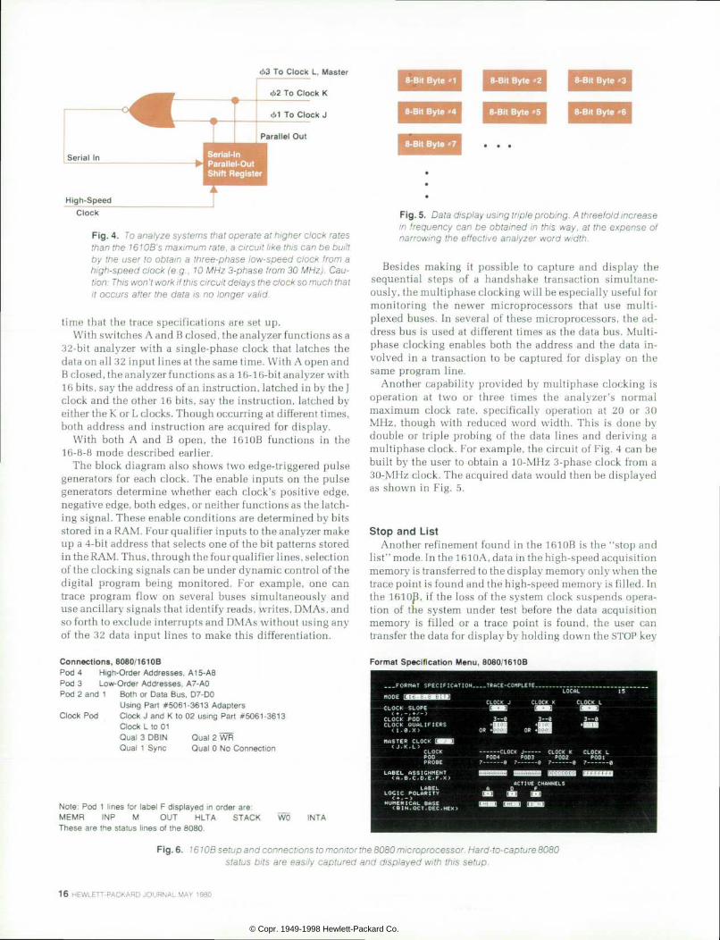
* 3 T o C l o c k L , M a s t e r
d > 2 T o C l o c k K
«¿1 To Clock J
P a r a l l e l O u t
Serial-ln Parallel-Out Shift Register
High-Speed Clock
Fig. 4. To analyze systems that operate at h igher c lock rates than the 16WB's maximum rate, a c i rcui t l ike th is can be bui l t by the user to ob ta in a th ree-phase low-speed c lock f rom a h igh-speed c lock (e .g . , 10 MHz 3-phase f rom 30 MHz) . Cau tion: This won't work if this circuit delays the clock so much that i t occurs af ter the data is no longer va l id .
time that the trace specifications are set up. With switches A and B closed, the analyzer functions as a
32-bit analyzer with a single-phase clock that latches the data on all 32 input lines at the same time. With A open and B closed, the analyzer functions as a 16-16-bit analyzer with 16 bits, say the address of an instruction, latched in by the J clock and the other 16 bits, say the instruction, latched by either the K or L clocks. Though occurring at different times, both address and instruction are acquired for display.
With both A and B open, the 1610B functions in the 16-8-8 mode described earlier.
The block diagram also shows two edge-triggered pulse generators for each clock. The enable inputs on the pulse generators determine whether each clock's positive edge, negative edge, both edges, or neither functions as the latch ing signal. These enable conditions are determined by bits stored in a RAM. Four qualifier inputs to the analyzer make up a 4-bit address that selects one of the bit patterns stored in the RAM. Thus, through the four qualifier lines, selection of the clocking signals can be under dynamic control of the digital program being monitored. For example, one can trace program flow on several buses simultaneously and use ancillary signals that identify reads, writes, DMAs, and so forth to exclude interrupts and DMAs without using any of the 32 data input lines to make this differentiation.
8 -B i t By te »1 I I 8 -B i t By te »2 I I 8 -B i t By te -3
8 - B i t B y t e  « 4 I I 8 - B i t B y t e " 5 I I 8 - B i t B y t e - 6
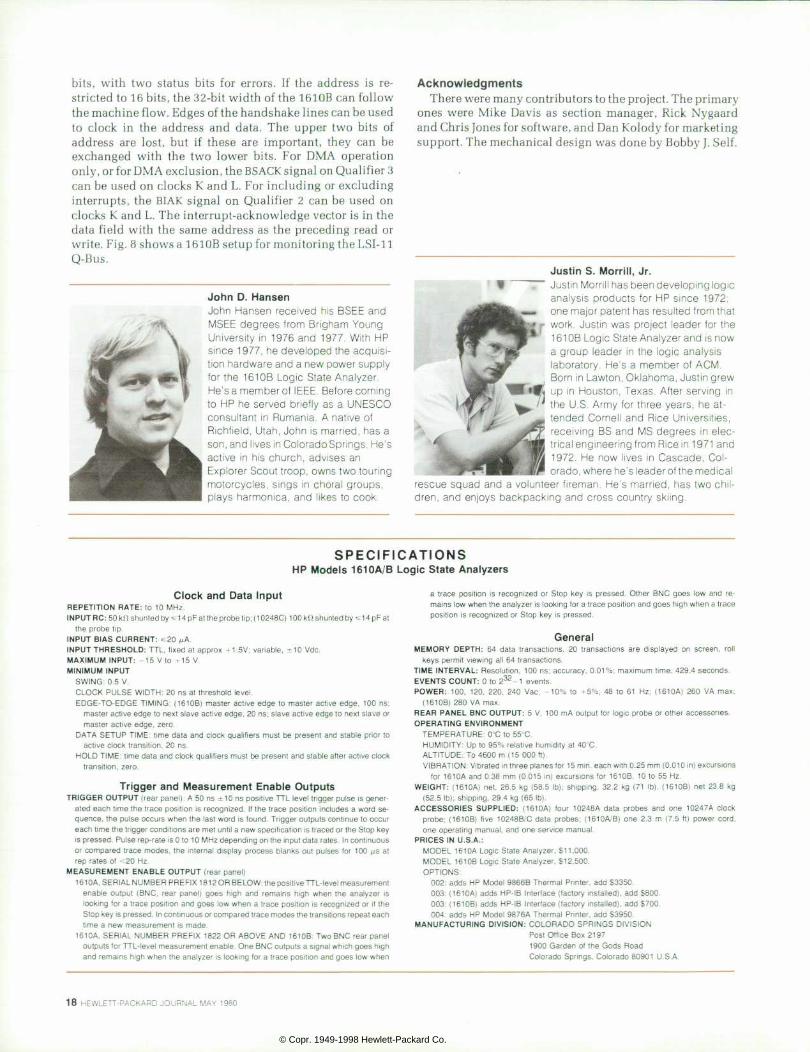
8-Bit Byte "7
Fig. 5. Data display using t r ip le probing. A threefold increase in f requency can be ob ta ined in th is way , a t the expense o f narrowing the ef fect ive analyzer word width.
Besides making it possible to capture and display the sequential steps of a handshake transaction simultane ously, the multiphase clocking will be especially useful for monitoring the newer microprocessors that use multi plexed buses. In several of these microprocessors, the ad dress bus is used at different times as the data bus. Multi phase clocking enables both the address and the data in volved in a transaction to be captured for display on the same program line.
Another capability provided by multiphase clocking is operation at two or three times the analyzer's normal maximum clock rate, specifically operation at 20 or 30 MHz, though with reduced word width. This is done by double or triple probing of the data lines and deriving a multiphase clock. For example, the circuit of Fig. 4 can be built by the user to obtain a 10-MHz 3-phase clock from a 30-MHz clock. The acquired data would then be displayed as shown in Fig. 5.
Stop and List Another refinement found in the 1610B is the "stop and
list" mode. In the 1610A, data in the high-speed acquisition memory is transferred to the display memory only when the trace point is found and the high-speed memory is filled. In the 1610B, if the loss of the system clock suspends opera tion of the system under test before the data acquisition memory is filled or a trace point is found, the user can transfer the data for display by holding down the STOP key
Connect ions, 8080/1610B P o d 4 H i g h - O r d e r A d d r e s s e s , A 1 5 - A 8 P o d 3 L o w - O r d e r A d d r e s s e s , A 7 - A O P o d 2 a n d 1 B o t h o r D a t a B u s , D 7 - D O
Us ing Par t #5061-3613 Adap te rs C l o c k P o d C l o c k J a n d K t o 0 2 u s i n g P a r t # 5 0 6 1 - 3 6 1 3
Clock L to 01 Q u a l 3 D B I N Q u a l 2 W R Q u a l 1 S y n c Q u a l O N o C o n n e c t i o n
Format Speci f icat ion Menu, 8080/1610B
C L O C K . P O D C L O C K Q U A L I F I E R S
< I , 0 , X >
< J , K , L > C L O C K P O D P R O B E
C L O C K J C L O C K K C L O C K L P 0 0 4 P 0 0 3 P O D 2 P O D I
7 A 7 a 7 a 7 a
Note: Pod 1 l ines for label F d isp layed in order are: M E M R I M P M O U T H L T A S T A C K W O These are the s tatus l ines of the 8080.
INTA
Fig. 6. Hard-to-capture OB setup and connections to monitor the 8080 microprocessor. Hard-to-capture 8080 s ta tus b i ts are eas i ly captured and d isp layed wi th th is se tup.
1 6 H E W L E T T - P A C K A R D J O U R N A L M A Y 1 9 8 0
© Copr. 1949-1998 Hewlett-Packard Co.

C o n n e c t i o n s . 8 0 6 5 , 1 6 1 0 8 P o d 4 H i g h - O r d e r A d d r e s s A 8 - A 1 5 Pod 3 and 2 Low-Orde r Add ress -Da ta ADO-AD7 w i t h adap te r P o d 1 S 1 S O I O / M R D W R S T D
6 5 7 4 3 2
Fo rma t Spec i f i ca t i on Menu 8085 1610B
Clock Pod
SID
C l o c k J A L E C l o c k K _ R D Qual 3 IO/M Qua l 1 SO
C lock L WR Qual 2 S1 Qual O No Connect ion
Fig. with connections 8085 microprocessor multiplexes part of the address with the data. The connections and setup shown a l low the 1610B to moni tor the 8085.
for more than two seconds. The memory contents are then displayed with the title line reading: HISTORY AT STOP. This technique is also useful for determining what the data is doing when the analyzer fails to find the trace point.
Demul t ip lex ing on Common Processors Here are three examples of the use of the 1610B's
multiple-phase qualified clocks for monitoring widely used processors. 8080. The 8080 is not usually thought of as a multiplexed processor, yet important information about each instruc tion cycle is contained in the status word that is multi plexed on the data bus at the beginning of each cycle. In many systems these status bits are difficult to get at or are only partially captured. Using a 1610B as shown in Fig. 6, the full status word can be captured and displayed. Storage qualification on this field allows the user to limit data capture to only interrupt acknowledge cycles, only stack operations, or only instruction fetches. Using the additional qualification available on the clocks, only reads or only writes on the bus can be selected. 8085. Instead of multiplexing the status bits, the 8085 mul tiplexes part of the address with the data. With the 1610B, the address can be entered, together with data, status, and control lines to specify the acquisition criteria. Qualifica
tion on the status lines allows selection of the machine cycles of interest, as shown in the table below. The only one not recognized is INA, which requires a clock change.
Control
8 0 8 5 M a c h i n e C y c l e C h a r t
M a c h i n e C y c l e S t a t u s I O / M S i S O
O P C O D E F E T C H ( O F ) 0 1 1 M E M O R Y R E A D ( M R ) 0 1 0 M E M O R Y W R I T E ( M W ) 0 0 1 I / O R E A D ( I O R ) 1 1 0 I / O W R I T E ( I O W ) 1 0 1 ACKNOWLEDGE O F I N T R ( I N A ) , 1 1 1 B U S I D L E ( B I ) D A D 0 1 0
ACK.OF R S T . T R A P 1 1 1 H A L T T S 0 0
TS =High Impedance State
Fig. 7 shows how the 1610B can be set up to monitor the 8085. LSI-11. The LSI-11 Q-Bus is an 18-bit, asynchronous bus with data and address multiplexed. Data width is 16
•Intel Component Data Catalog. 1980. "Reg is te red t rademark . D ig i ta l Equ ipment Corpora t ion .
C o n n e c t i o n s , L S I - 1 1 Q - B u s 1 6 1 0 B F o r m a t S p e c i f i c a t i o n M e n u L S I - 1 1 Q - B u s 1 6 1 0 B Pod 4, 2 Pod 3, 1 Clock Pod
For DMA For INT Vector
H igh-Order Address /Data BDAL15 - BDAL8 Low-Order Address /Data BDAL7 - BDALO C l o c k J B S Y N C C l o c k K B D I N C l o c k L B D O U T Clock K or L Clock K or L
(Add ress ) ( - ) (Read Data ) (+ ) (Wr i te Data) (+) Qua l 3 BSACK Qual 2 BIAK Qual 3 No Connect ion Qual 4 No Connect ion
Fig. Corporation's 76706 setup and connections to monitor Digital Equipment Corporation's LSI- 1 1 Q-Bus, an 18-b i t asynchronous bus w i th addresses and da ta mu l t ip lexed.
M A Y 1 9 8 0 H E W L E T T - P A C K A R D J O U R N A L 1 7
© Copr. 1949-1998 Hewlett-Packard Co.
bits, with two status bits for errors. If the address is re stricted to 16 bits, the 32-bit width of the 1610B can follow the machine flow. Edges of the handshake lines can be used to clock in the address and data. The upper two bits of address are lost, but if these are important, they can be exchanged with the two lower bits. For DMA operation only, or for DMA exclusion, the BSACK signal on Qualifier 3 can be used on clocks K and L. For including or excluding interrupts, the BIAK signal on Qualifier 2 can be used on clocks K and L. The interrupt-acknowledge vector is in the data field with the same address as the preceding read or write. Fig. 8 shows a 1610B setup for monitoring the LSI-11 Q-Bus.
J o h n D . H a n s e n John Hansen rece ived h is BSEE and MSEE degrees f rom Br igham Young Univers i ty in 1976 and 1977. Wi th HP s ince 1977, he deve loped the acqu is i t ion hardware and a new power supply for the 161 OB Logic State Analyzer. He's a member of IEEE. Before coming to HP he served br ie f l y as a UNESCO consul tant in Rumania. A nat ive o f Richf ie ld, Utah, John is marr ied, has a son, and l ives in Colorado Springs. He's act ive in h is church, adv ises an Explorer Scout t roop, owns two tour ing motorcyc les , s ings in chora l groups, p lays harmonica, and l ikes to cook.
Acknowledgments There were many contributors to the project. The primary
ones were Mike Davis as section manager, Rick Nygaard and Chris Jones for software, and Dan Kolody for marketing support. The mechanical design was done by Bobby J. Self.
Jus t i n S . Me r r i l l , J r . W ~ ~ J u s t i n M o r r i l l h a s b e e n d e v e l o p i n g l o g i c
analys is products for HP s ince 1972; I feL — • one major patent has resulted from that
•Mr work . Jus t in was p ro jec t l eader fo r the 161 OB Logic State Analyzer and is now a group leader in the log ic ana lys is
. . Â ¿ r . ; l a b o r a t o r y . H e ' s a m e m b e r o f A C M . Born in Lawton, Oklahoma, Just in grew up in Houston, Texas. Af ter serv ing in the U.S. Army fo r th ree years , he a t tended Cornel l and Rice Univers i t ies , r ece i v i ng BS and MS deg rees i n e lec trical engineering from Rice in 1 971 and 1972 . He now l i ves in Cascade , Co l orado, where he's leader of the medical
rescue squad and a vo lun teer f i reman. He 's mar r ied , has two ch i l d ren , and en joys backpack ing and c ross count ry sk i ing .
S P E C I F I C A T I O N S H P M o d e l s 1 6 1 0 A / B L o g i c S t a t e A n a l y z e r s
C l o c k a n d D a t a I n p u t REPETIT ION RATE: t o 10 MHz . INPUT RC: 50 k!i shunted by «1 4 pF at the probe tip; (10248C) 1 00 kil shunted by «1 4 pF at
the probe t ip. INPUT BIAS CURRENT: «20 /¿A. INPUT THRESHOLD: TTL, f i xed a t approx +1.5V; var iab le , ±10 Vdc. M A X I M U M I N P U T : - 1 5 V t o + 1 5 V . M IN IMUM INPUT
SWING: 0 .5 V . CLOCK PULSE WIDTH: 20 ns a t th resho ld leve l . EDGE-TO-EDGE T IMING: (1610B) mas te r ac t i ve edge to mas te r ac t i ve edge , 100 ns ;
master s lave edge to next s lave act ive edge, 20 ns; s lave act ive edge to next s lave or master act ive edge, zero.
DATA SETUP TIME: t ime da ta and c lock qua l i f ie rs must be p resent and s tab le p r io r to act ive clock transi t ion, 20 ns.
HOLD stable t ime data and c lock qual i f iers must be present and stable af ter act ive c lock transit ion, zero.
T r i g g e r a n d M e a s u r e m e n t E n a b l e O u t p u t s TRIGGER OUTPUT (rear panel ) : A 50 ns ±10 ns posi t ive TTL level t r igger pulse is gener
ated posit ion t ime the trace posit ion is recognized. I f the trace posit ion includes a word se quence, occur pulse occurs when the last word is found. Trigger outputs continue to occur each t ime the tr igger condit ions are met unti l a new specif icat ion is traced or the Stop key is pressed. Pulse rep-rate is 0 to 10 MHz depending on the input data rates. In continuous or compared t race modes, the in te rna l d isp lay process b lanks out pu lses fo r 100 ps a t rep ra tes o f <20 Hz.
M E A S U R E M E N T E N A B L E O U T P U T ( r e a r p a n e l ) 1610A, measurement NUMBER PREFIX 181 2 OR BELOW: the positive TTL-level measurement
e n a b l e i s ( B N C , r e a r p a n e l ) g o e s h i g h a n d r e m a i n s h i g h w h e n t h e a n a l y z e r i s looking the a t race posi t ion and goes low when a t race posi t ion is recognized or i f the Stop key is pressed. In continuous or compared trace modes the transit ions repeat each t ime a new measurement i s made.
1610A , SERIAL NUMBER PREFIX 1822 OR ABOVE AND 1610B: Two BNC rea r pane l outputs for TTL- level measurement enable. One BNC outputs a s ignal which goes high and remains h igh when the analyzer is looking for a t race posi t ion and goes low when
a t r a c e r e i s r e c o g n i z e d o r S t o p k e y i s p r e s s e d . O t h e r B N C g o e s l o w a n d r e mains low when the analyzer is looking for a trace posit ion and goes high when a trace posi t ion is recognized or Stop key is pressed.
General M E M O R Y r o l l 6 4 d a t a t r a n s a c t i o n s , 2 0 t r a n s a c t i o n s a r e d i s p l a y e d o n s c r e e n , r o l l
keys permit v iewing al l 64 t ransact ions. T I M E t i m e , R e s o l u t i o n , 1 0 0 n s ; a c c u r a c y , 0 . 0 1 % ; m a x i m u m t i m e , 4 2 9 . 4 s e c o n d s . E V E N T S C O U N T : 0 t o 2 3 2 - 1 e v e n t s . P O W E R : 1 0 0 , 1 2 0 , 2 2 0 , 2 4 0 V a c ; - 1 0 % t o + 5 % ; 4 8 t o 6 1 H z ; ( 1 6 1 0 A ) 2 6 0 V A m a x ;
(1610B) 280 VA max. REAR accessories. BNC OUTPUT: 5V, 100 mA output for logic probe or other accessories. O P E R A T I N G E N V I R O N M E N T
TEMPERATURE: O'C to 55°C. HUMIDITY: Up to 95% relat ive humidity at 40°C. ALTITUDE: To 4600 m (15 000 f t ) . VIBRATION: Vibrated in three planes for 15 mm. each with 0.25 mm (0.010 in} excursions
for 1610A and 0 .38 mm (0 .015 in) excurs ions for 1610B, 10 to 55 Hz. W E I G H T : k g n e t , 2 6 . 5 k g ( 5 8 . 5 I b ) ; s h i p p i n g , 3 2 . 2 k g ( 7 1 I b ) . ( 1 6 1 0 B ) n e t 2 3 . 8 k g
(52.5 Ib): shipping, 29.4 kg (65 Ib). A C C E S S O R I E S S U P P L I E D : ( 1 6 1 0 A ) f o u r 1 0 2 4 8 A d a t a p r o b e s a n d o n e 1 0 2 4 7 A c l o c k
p r o b e ; c o r d , f i v e 1 0 2 4 8 B / C d a t a p r o b e s ; ( 1 6 1 0 A / B ) o n e 2 . 3 m ( 7 . 5 f t ) p o w e r c o r d , one operat ing manual , and one serv ice manual .
PRICES IN U.S.A. : MODEL 1610A Log ic Sta te Ana lyzer , $11,000. MODEL 1610B Log ic Sta te Ana lyzer , $12,500. OPTIONS:
002: adds HP Model 9866B Thermal Pr in ter , add $3350. 003 : $800 . adds HP- IB In te r face ( fac to ry ins ta l led ) , add $800 . 003: (1610B) adds HP-IB Inter face ( factory insta l led) , add $700. 004: adds HP Model 9876A Thermal Pr in ter , add $3950.
M A N U F A C T U R I N G D I V I S I O N : C O L O R A D O S P R I N G S D I V I S I O N Post Off ice Box 21 97 1 900 Garden of the Gods Road Colorado Spr ings. Colorado 80901 U.S.A.
1 8 H E W L E T T - P A C K A R D J O U R N A L M A Y 1 9 8 0
© Copr. 1949-1998 Hewlett-Packard Co.
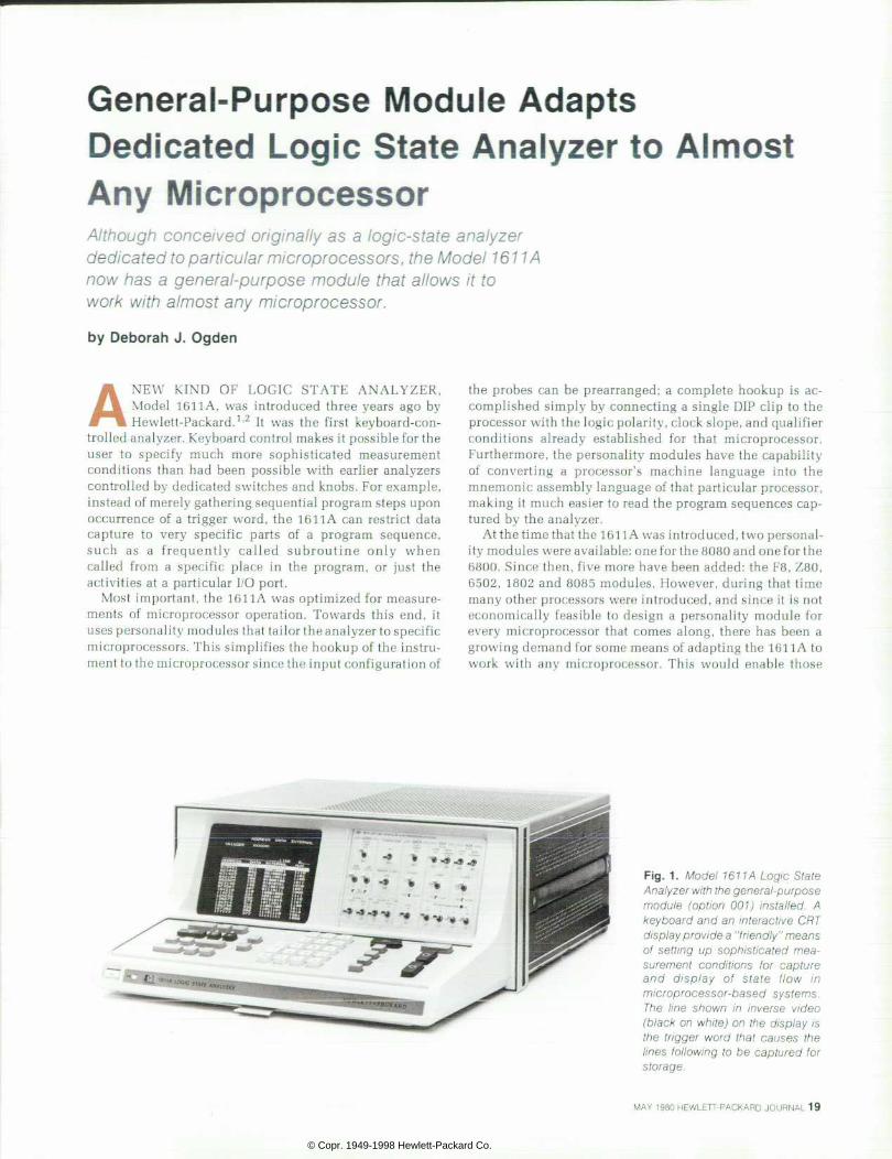
Genera l -Purpose Module Adapts Dedicated Logic State Analyzer to Almost Any Microprocessor Al though conceived or ig ina l ly as a log ic-s ta te analyzer dedicated to part icular microprocessors, the Model 161 1A now has a genera l -purpose module that a l lows i t to work wi th a lmost any microprocessor .
by Deborah J . Ogden
ANEW KIND OF LOGIC STATE ANALYZER, Model 1611A, was introduced three years ago by Hewlett-Packard.1'2 It was the first keyboard-con
trolled analyzer. Keyboard control makes it possible for the user to specify much more sophisticated measurement conditions than had been possible with earlier analyzers controlled by dedicated switches and knobs. For example, instead of merely gathering sequential program steps upon occurrence of a trigger word, the 1611A can restrict data capture to very specific parts of a program sequence, such as a frequently cal led subroutine only when called from a specific place in the program, or just the activities at a particular I/O port.
Most important, the 1611A was optimized for measure ments of microprocessor operation. Towards this end, it uses personality modules that tailor the analyzer to specific microprocessors. This simplifies the hookup of the instru ment to the microprocessor since the input configuration of
the probes can be prearranged; a complete hookup is ac complished simply by connecting a single DIP clip to the processor with the logic polarity, clock slope, and qualifier conditions already established for that microprocessor. Furthermore, the personality modules have the capability of converting a processor's machine language into the mnemonic assembly language of that particular processor, making it much easier to read the program sequences cap tured by the analyzer.
At the time that the 1611A was introduced, two personal ity modules were available: one for the 8080 and one for the 6800. Since then, five more have been added: the F8, Z80, 6502, 1802 and 8085 modules. However, during that time many other processors were introduced, and since it is not economically feasible to design a personality module for every microprocessor that comes along, there has been a growing demand for some means of adapting the 161 1 A to work with any microprocessor. This would enable those
F ig . 1 . Mode l 1611 A Log ic S ta te Analyzer with the general-purpose modu le (op t i on 001 ) i ns ta l l ed . A keyboard and an in te rac t i ve CRT display provide a "fr iendly1' means o f s e t t i n g u p s o p h i s t i c a t e d m e a s u r e m e n t c o n d i t i o n s f o r c a p t u r e a n d d i s p l a y o f s t a t e f l o w i n m i c r o p r o c e s s o r - b a s e d s y s t e m s . T h e l i n e s h o w n i n i n v e r s e v i d e o (b lack on whi te) on the d isp lay is t he t r i gge r wo rd t ha t causes t he l ines fo l low ing to be cap tured fo r storage.
M A Y 1 9 8 0 H E W L E T T - P A C K A R D J O U R N A L 1 9
© Copr. 1949-1998 Hewlett-Packard Co.

designing with microprocessors not covered by existing modules to make use of the powerful'triggering capabilities of the 1611 A. Accordingly, a program was instituted to develop a general-purpose module able to handle virtually any microprocessor.
Formulat ing a Design Defining such a module turned out to be a major project in
itself. To begin with, it was obvious that listing program sequences in mnemonics is in direct conflict with a general-purpose thrust, since the mnemonics are pro cessor-dependent. For the same reason, prearranged hookups could not be provided because the pin configura tions of microprocessors differ.
However, other capabilities could be added to increase flexibility. One is multiple clocking, a necessity for the newer microprocessors that multiplex information on their buses. For example, one microprocessor uses an 8-bit bus for 16-bit addresses by sequencing the upper and lower bytes. On others, one bus carries both address and data information at different times. Even if a microprocessor does not multiplex its buses, some of the other pins may have different information at different times.
With the multiple clocking designed into the general- purpose module for the 1611 A, one clocking event can be used to strobe in the least-significant byte of an address and another the most-significant byte (Fig. 2). A third event can be used to trigger the gathering of data in the 8-bit field known as the EXTERNAL field, and a fourth for the 4-bit AUXILIARY field. Three clocks, each of which can be qual ified, can be ORed together to generate a strobe for the 8-bit DATA field. The ORed clock can be very useful because the data bus of some microprocessors is not valid on the same clocking event for every type of instruction. This clock can
also be used with the other fields. For example, the EXTER NAL and AUXILIARY fields can be strobed in with the ORed clock rather than with their own dedicated strobes.
One of the clocks for the DATA, EXTERNAL, or AUXILIARY fields may be designated as the MASTER clock that strobes the gathered information into the display memory. Each line of the display may then show the activity that occurred on all the monitored lines during that instruction cycle.
Each of the seven clock inputs can be set individually to respond to either the rising or the falling edge of the corre sponding clock signal.
Display Formatt ing Until recently, most widely available microprocessors
had an 8-bit data bus. Now, several processors with 16-bit data buses are available. This affects how the data is to be displayed on the logic analyzer. Like the dedicated mod ules, the general-purpose module allows collection of 36-bit words. However, since it can interrogate most any 8- or 16-bit microprocessor-based system, the option of for matting the display is provided. For 8-bit microprocessors, the usual format is a 16-bit ADDRESS field, an 8-bit DATA field, and 12 bits for other signals in the EXTERNAL and AUXILIARY fields (Fig. 3). The most desirable format for 16-bit machines is a 16-bit ADDRESS field and a 16-bit DATA field. A switch on the front panel of the general-purpose module enables the user to combine the 8-bit DATA field with the 8-bit EXTERNAL field for display as a 16-bit DATA field. Four bits are still available for auxiliary signals.
The ADDRESS and DATA fields may be displayed in either octal or hexadecimal base. The EXTERNAL and AUXILIARY fields may be displayed in binary as well as in octal or hexadecimal.
' ' 1 A O P T 0 0 1 ' F O R 8 O B ' Â « B I T P O O C E S S O R S Y S T E M S !
A D R S D A T A T X T
M S B L S B C L O C K C L O C K M A :
x \
• • CLOTk
EDGE r
* All X
BIN
•
§
I t
F i g . 2 . F r o n t p a n e l o f t h e g e n e r a l - p u r p o s e m o d u l e f o r t h e 1 6 1 1 A L o g i c S t a t e A n a l y z e r . S e v e n c l o c k i n p u t s e n a b l e i n f o r mation on several buses to be cap tured for s imul taneous d isplay.
2 0 H E W L E T T - P A C K A R D J O U R N A L M A Y 1 9 8 0
© Copr. 1949-1998 Hewlett-Packard Co.

A D D R E S S 0 F 1 6
A D D R E S S D A T A E X T E R N A L
I I H E E X T E R N A L A U X
0011 F F e o n FF F F 0 0 1 1 F F 0 0 1 1 F F 0 0 0 ,
0 0 1 1 F F 0 0 1 1
0 0 1 1 F F 0 0 1 1
F F 0 0 1 1 F F 0 0 1 1
0 0 0 1
0 0 1 1 F F 0 0 1 1
A D D R E S S D A T A E X T E R N A L
T R I G G E R 0 0 4 8
T R I G R O C C U R = 5
A D D R E S S D t l T f t 0 0 4 0 5 0 0 2 0 0 4 1 6 0 0 B 0 0 4 2 6 4 0 e 0 0 4 3 D 0 7 B 0 0 - 0 0 0 0 2
0 0 4 4 5 C 0 0 0 0 4 5 7 8 F F 5 0 4 6 1 9 F C 0 0 4 3 D 0 7 S 0 0 7 0 0 0 0 1 0 0 4 4 5 C 0 0 0 0 4 5 7 8 F F 0 0 4 7 5 1 0 0 0 0 4 8 7 9 0 1 0 0 4 3 Ã 1 F E 0 0 4 8 7 9 0 1
P R E - T R I G R = 2 5 L I N E
F ig . 3 . Fo r an 8 -b i t m i c rop roces so r t he d i sp lay can be fo rma t ted with a 16-bit ADDRESS field, an 8-bit DATA f i e l d , and 12 b i t s f o r o the r s i gna l s ( l e f t ) . Fo r a 16 -b i t m ic ro p rocessor , the d isp lay can be fo r matted with a 16-bit ADDRESS field and a 1 6-bit DATA field with four bits remaining for other signals (r ight). The ADDRESS and DATA fields can be d i s p l a y e d i n e i t h e r o c t a l o r hexadecimal .
Some processors operate certain buses with negative logic polarity. A switch for each of the display fields (AD DRESS, DATA, EXTERNAL and AUXILIARY) on the general- purpose module allows a choice of positive or negative logic for that field. If a switch is set for negative polarity, the software inverts data appearing on the bus before display ing it. Also, when the user enters a trigger word, it is dis played on the screen as entered, but if negative polarity has been selected for that field, the software inverts the data before loading it into the trigger comparators.
Mainframe Compatibi l i ty The general-purpose module functions with any stan
dard 1611A, so functions available through the 1611A keyboard are recognized. This includes trigger specifica tions and run commands. The only exception is that the MNEMONIC/ABSOLUTE key is disabled by the module's software.
Capabilities unique to the general-purpose module, such as clock selection, are interfaced to the user by way of the module's front panel.
Although this module will probably find most use in sorting out the complex word patterns of today's high- performance, multiplex-structured microprocessors, its capabilities also suggest its use for: • Monitoring data flow across a parallel I/O structure; • Investigating the status of control flags with respect to
specific bus activity; • Making time measurements across asynchronous func
tional circuit blocks.
Mechanical Considerat ions Each type of processor has a different pin configuration.
Although most come in 40-pin DIPs, there are other sizes and shapes and in the case of bit-slice processors, no single chip has a whole bus. The general-purpose module there fore has a flexible scheme for hooking up to the system under test. Altogether, the module has 46 inputs: 16 AD DRESS lines, 8 DATA lines, 8 EXTERNAL lines, 4 AUXILIARY lines, 7 clock lines, and 3 qualifiers. These are grouped into two probe pods. Connections are made with individual leads and miniature probe tips that have removable pincher-type probes (see Fig. 4). The pinchers are small enough to permit placement on adjacent pins of a standard DIP but may be removed to permit the probe tip to be slipped over the pins of a DIP-clip.
As a further convenience, the probe module to which the
leads are attached can be unplugged from the probe body, exposing an edge connector that can be plugged onto a printed-circuit board that has a connector specifically wired as a test port. For particular hookups that must be "remembered," Model 10277D General Purpose Probe In terface has plug-in sockets for the two probes and a wire- wrap patch panel for prearranging the input leads.
Implementat ion The block diagram of the 1611 A shown in Fig. 5 indicates
which functions reside on the mainframe and which are in the personality module. One of the first hardware chal lenges in designing the new general-purpose module was how to coordinate the gathering of data from all the various fields being strobed by clocks that may occur at different times. The problem was how to tell when every field has been gathered for one cycle, so that the information for that cycle can be stored together, and the next clocks that occur will store the fields for the next cycle. This problem was solved by allowing the user to select the MASTER clock. A switch on the front panel (Fig. 2) allows the user to indicate whether the DATA, EXTERNAL, or AUXILIARY strobe indi cates "cycle complete." As shown in Fig. 6, each field is strobed into a storage buffer when its particular clock oc curs, a the contents of all these buffers are latched into a second buffer when the clock chosen as MASTER occurs.
Fig. 4 . The versat i le probing scheme for the 161 1A Opt 001 permits a variety of methods for connecting the analyzer to the uni t to be tested.
MAY 1980 HEWLETT-PACKARD JOURNAL 21
© Copr. 1949-1998 Hewlett-Packard Co.

Components of Personal i ty Module Components of 1611 A Mainframe
From System under Test
Comparators
Display Storage and
Character Generator
F i g . 5 . B l o c k d i a g r a m o f t h e 161 1A Logic State Analyzer. Data enters the 1611 A through a set of bu f fe rs and i s temporar i l y s to red accord ing to the t im ing o f the m i croprocessor under test. This data i s then s to red se lec t i ve ly accord ing to user-entered condit ions and i s d i s p l a y e d b y t h e 1 6 1 1 A . K e y board-entered user condi t ions are f o r m a t t e d b y t h e 1 6 1 1 A m i c r o p r o c e s s o r a n d l o a d e d i n t o compara to rs , whe re t hey can be compared w i th incoming data .
Another challenge involved the time period during which the user's data inputs must be valid with respect to the associated clocks, generally referred to as the setup and hold times (Fig. 7). The data has to be valid for some period in the vicinity of the clock, because within the logic analyzer, the data and the clocks go through buffers and other circuits that have various time delays associated with them. By the time the data is strobed into the storage buffer
LSB ADRS
LSB Strobe
M S B A D R S .
M S B S t r o b e ,
D A T A
D A T A Strobe
E X T
EXT Strobe
A U X
AUX Strobe .
Storage B u f f e r o 8 Bits
Storage B u f f e r o 8 Bits
Storage Buffer Q 8 Bits
Storage Buffer 4 Bits
Storage Buffer
36 Bits
I To Selected I Storage and I Comparators
Master Clock
in the module, the various bits may not be aligned with respect to time exactly as they were when they entered the analyzer. They will, however, be lined up within certain limits. After the timing specifications of many micro processors had been studied, it was decided to set the limits so that the hold time would be zero and the setup time as small as possible — many microprocessors do not require the data on the buses to remain valid after the correspond ing clock, but most have a setup time specified.
To obtain zero hold time, the delays in the module's clock circuits must always be less than the delays in the data circuits. To assure this, Schottky TTL is used in the new module's clock paths to minimize these delays while delay lines are used in the data paths. The delay lines were chosen to assure that for worst case conditions, the data is slowed just enough to arrive at the latches simultaneously with the clocks. By computing the fastest possible clock path and the slowest possible data path, the minimum setup time was calculated to be 80 ns.
Examples To see how the 1611 A is applied to analyses of micro
processor operations with the new module (Option 001), let
Data to Be Gathered
Clock Input
TV = T ime dur ing which data must be val id to assure i t is gathered properly
TH = Hold t ime Ts = Setup t ime
Fig. 6. The temporary storage port ion of the general-purpose m o d u l e u s e s a d o u b l e - b u f f e r i n g s c h e m e t o i m p l e m e n t t h e master c lock concept .
Fig. 7. The data to be strobed into storage must be valid at the t ime the s t robe (c lock) occurs . The t im ing must account fo r any delays encountered in the logic state analyzer 's c i rcui ts.
2 2 H E W L E T T - P A C K A R D J O U R N A L M A Y 1 9 8 0
© Copr. 1949-1998 Hewlett-Packard Co.

T , T 2 T 3 T 4
CLK (8284 Output) J~
R E A D
A L E
A D i 5 - A D o
RD
A D , 5 - A D r
W R I T E
W R
A D 1 5 - A D 0
I N T A
I N T A
A d d
A d d
D a t a I n
D a t a O u t
P o i n t e r
Fig . 8 . Sus t im ing d iagram fo r the 8086 mic roprocessor .
us look at a couple of examples. First, the Intel 8086. This is a 16-bit microprocessor that multiplexes addresses and data on one bus. Hence, the analyzer's probe lines for data are connected to the same points in the system as the probe lines for addresses. The display is formatted to contain a 16-bit ADDRESS field, a 16-bit DATA field, and four AUX ILIARY bits.
Since the address information and data information are valid at different times, multiple clocks are used to gather these two fields in the same instruction cycle. As shown in the timing diagram of Fig. 8, the address field is clocked in on the falling edge of the address latch enable signal (ALE). To capture data on all memory read cycles, memory write cycles, and interrupt cycles, the data clock is the ORed combination of the rising edge of RD, the rising edge of WR,
A D D R E S S 0 F 1 6 0F171 0 F 1 8 0 F 1 F 0 F 2 0 0 F 2 1 0 F T 1 0 F 2 2 0 F 2 3 0 F 2 4 0 F 2 5 0 F 2 6 0 F 2 7 0 F 2 8 0 F 1 S 0 F 1 6
A D D R E S S D A T A E X T E R N A L
L Â · I N E EXTERNAL FF FF FF FF FF FF FF FF FF FF FF FF FF FF FF FF
F i g . 1 0 . T r a c e l i s t g e n e r a t e d w h i l e t h e 1 6 1 1 A O p t 0 0 1 moni tors a SC/MP microprocessor sys tem.
and the rising edge of INTA. The control lines can be monitored to provide additional
insights into the processor's activity. Bit 0 of the auxiliary field can trace activity on the DT/R (data transmit/receive) line and bit 1 can be connected to the M/IO (memory/input- output) line. The two most significant bits are not used here.
The control line states for the first five lines of the listing of program flow shown in Fig. 9 indicate memory reads, and by the addresses it is seen that they are reads from ROM space. The sixth line is also a read, but it is to a RAM address. The eighth line of the listing indicates a write to an I/O port followed by signal fetches from ROM. Line 13 is a memory write to a RAM address.
To monitor an 8-bit processor such as the National SC/MP, the display is formatted to contain a 16-bit ADDRESS field, an 8-bit DATA field, an 8-bit EXTERNAL field for such data as that to and from an I/O port, and a 4-bit AUXILIARY field (Fig. 10).
The SC/MP is a 40-pin processor with 16-bit addressing
A D D R E S S D A T A E X T E R N A L
T R I G G E R
V a l i d 1 2 - B i t A d d r e s s A d d r e s s
Bus x : V a l i d 1 2 - B i t A d d r e s s
A D D R E S S F 2 S Â » 5 F 2 9 6 F 2 S > 8 F 2 9 A F 2 S Â » C 0 0 6 2 F 2 9 E F F E 8 F 2 A 0 0 0 5 F
L I N E E X T E R N A L
3 AUX 1110 1110 1110 1 1 1 0
1 1 1 0
1 1 1 0
1 1 1 0
V a l i d V a l i d I / O O u t p u t
S t a t u s D a t a
Valid I/O
Valid Input
Data Bus
NADS (Address Strobe)
S t a t u s D a t a
DOOOC
~LJ
F 2 6 C F 2 6 E
Fig. 9. Trace l ist ing of transactions in an 8086 microprocessor system presents the 16-bit ADDRESS and DATA information in hexadecimal and the AUXILIARY information in binary.
V f
One or the Other Occurs
NRDS (Read Strobe)
Fig . 11 . T im ing d iagram fo r the SC/MP mic roprocessor .
M A Y 1 9 8 0 H E W L E T T - P A C K A R D J O U R N A L 2 3
© Copr. 1949-1998 Hewlett-Packard Co.

capability, 8-bit data handling, and 22 control, clock, and flag signals. To accommodate this many signals, the chip's pinout multiplexes the data on the DATA bus with four address bits and four status bits. Therefore, when connect ing the 1611 A Opt 001 to the system under test, the DATA bus is double-probed. Four bits are shared by DATA and ADDRESS and the other four bits are shared by DATA and AUXILIARY.
Demultiplexing the DATA bus for the 1611A Opt 001 requires a combination of three clocks from the SC/MP. A timing diagram is shown in Fig. 11. The DATA bus, DBO- DB7, carries input data when the negative read data strobe (NRDS) is true and output data when the negative write data strobe (NWDS) is true. When the negative address ready strobe (NADS) is true, DATA bus lines DBO through DB3 carry the upper four address bits and lines DB4 through DB7 carry processor status flags. The DATA field strobe for the 161 1 A is the ORed combination of the rising edge of NRDS and the rising edge of NWDS. The ADDRESS and AUXILIARY strobes are the rising edge of NADS.
Fig. 10 is a typical trace list of a SC/MP microprocessor as monitored by the 1611A Opt 001. The control lines con nected to the AUXILIARY field simplify interpretation of the display. Auxiliary bit 0 monitors the RFLG line which is high (1) when data is being input to the processor. Bit 1, the instruction flag, denotes the first byte of each instruction. Monitoring these two control lines makes rapid decoding of the display possible. For example, in Fig. 10, line 1 of the display shows a 1-cycle fetch of 08 from location OF16, lines 5 and6area2-cyclefetchof C8and 50 followed by a 1-cycle output execution that stores 00 in location OF71.
Acknowledgments Jeff Smith, Justin Morrill, and PeteRawson contributed to
the module's design. Roger Molnar did the product design and Bill Furch the production engineering. Don Corson provided marketing support including invaluable assis tance in the creation of this article.
Reference 1. J.H. Smith, "A Logic State Analyzer for Microprocessor Sys tems," Hewlett-Packard Journal, January 1977. 2. T.A. Saponas, "Firmware for a Microprocessor Analyzer," Hewlett-Packard Journal, January 1977.
S P E C I F I C A T I O N S H P M o d e l 1 6 1 1 A O p t i o n 0 0 1 L o g i c S t a t e A n a l y z e r
G e n e r a l P u r p o s e P e r s o n a l i t y M o d u l e NOTE: Model 10264A persona l i ty module may be ordered separa te ly (or ins ta l la t ion in a 1611 A to provide Opt ion 001 capabi l i ty.
INPUTS INPUT CURRENT: Approx. 200 /¿A logic 0 ( low); approx. 20 /¿A logic 1 (high). THRESHOLD: 2V min. logic 1 (high); 0.7V max. logic 0 ( low). Al l inputs have hysteresis INPUT CAPACITANCE: Approx . 20 pF .
CLOCK CLOCK 1A dc to 2 .8 MHz max. (2 .2 MHz max. i f ins ta l led in 161 1A wi th ser ia l number
o f 1723A o r ea r l i e r ) . M in imum pu lse w id th i s 30 ns . No c lock shou ld occu r un t i l a t least period ns after the master clock. The NO CLOCK indicator lights if the period between c locks exceeds 4 ms.
S E T U P A N D H O L D T I M E S SETUP TIME: 80 ns re lat ive to speci f ied c lock edge. HOLD TIME: Zero.
PRICE IN U.S.A. : 1611A Opt ion 001, $6000. 10264A, $2000. M A N U F A C T U R I N G D I V I S I O N : C O L O R A D O S P R I N G S D I V I S I O N
Post Of f ice Box 2197 1900 Garden o f the Gods Road Colorado Spr ings, Colorado 80901
D e b o r a h J . O g d e n Debb ie Ogden ho lds a BS degree in computer science and an MS degree in e lec t r ica l eng ineer ing , awarded by North Carol ina State Universi ty in 1974 and 1 976. A development engineer with HP's Colorado Spr ings Div is ion s ince 1976, she developed the F8, Z80, and genera l -purpose persona l i ty modules for the 1611 A Logic State Analyzer. Now wi th HP's Boise, Idaho Div is ion, she 's deve lop ing mic roprocessor sof tware for tape dr ives and s tudy ing for her MBA degree part-t ime. Debbie is marr ied and l ives in Boise. She's a
fà f l member o f Toastmasters and en joys nòrd ic and a lp ine sk i ing, cyc l ing, h ik ing, camping, and sa i l ing her recent ly acqui red 16- foot Hobie Cat .
.,
/
Address Cor rec t ion Reques ted Hewle t t -Packard Company , 1501 Page Mi l l
Road, Palo Al to , Cal i forn ia 94304
H E W L E T T - P A C K A R D J O U R N A L
Bulk Rate U.S. Postage
Paid Hewlett-Packard
Company
M A Y 1 9 8 0 V o l u m e 3 1 â € ¢ N u m b e r 5
T e c h n i c a l I n f o r m a t i o n f r o m t h e L a b o r a t o r i e s o f H e w l e t t - P a c k a r d C o m p a n y
Hewle t t -Packard Company , 1501 Page M i l l Road Palo Al to, Cal i forn ia 94304 U.S A.
Hewle t t -Packard Cent ra l Ma i l ing Depar tment Van Heuven Goedhar t laan 121
1 1 8 0 A M A m s t e l v e e n T h e N e t h e r l a n d s Yokogawa-Hewle t t -Packard L td , Sug inami -Ku
Tokyo 1 68 Japan
J O H N S H O P K N R D 20810
/ ""N I I A K I S~\ f "~ S~\ ^ A r~N râ„¢\ f "**) f "~ ^ ^^ . To change your address or delete your name from our mai l ing l is t p lease send us your old address label . Send \ _ / I I r \ I N V j l t W r / A L / L J I l t O O . c h a n g e s t o H e w l e t t - P a c k a r d J o u r n a l , 1 5 0 1 P a g e M i l l R o a d , P a l o A l t o . C a l i f o r n i a 9 4 3 0 4 U . S . A . A l l o w 6 0 d a y s .
© Copr. 1949-1998 Hewlett-Packard Co.