ÝÝÝhßÙÒÉÊhÉÕÓhÚÝ v.2.pdf · document version: 3 . date: 2004/06/17. customer : dell /...
TRANSCRIPT

Document Version: 3
Date: 2004/06/17
Customer : Dell / Wistron
Product Functional Specification
12.1 inch Wide XGA Color TFT LCD Module Model Name: B121EW01 V2
Final Specification
Note: This Specification is subject to change without notice.
(C) Copyright AU Optronics
Dec., 2003 All Rights Reserved. B121EW01 V2
No Reproduction and Redistribution Allowed. 1/25
www.yslcd.com.tw
Contents
1.0 Handling Precautions ....................................................................................................................... 4 2.0 General Description............................................................................................................................ 5 2.1 Display Characteristics ...................................................................................................................... 5 2.2 Functional Block Diagram.................................................................................................................. 6 3.0 Absolute Maximum Ratings............................................................................................................... 7 4.0 Optical Characteristics....................................................................................................................... 8 5.0 Signal Interface ................................................................................................................................... 9 5.1 Connectors .......................................................................................................................................... 9 5.2 Signal Pin............................................................................................................................................. 9 5.3 Signal Description ............................................................................................................................ 10 5.4 Signal Electrical Characteristics ..................................................................................................... 10 5.5 Signal for Lamp connector ...............................................................................................................11 6.0 Pixel Format Image ........................................................................................................................... 12 7.0 Parameter guide line for CCFL Inverter .......................................................................................... 12 8.0TimingControl…………………………………………………………………………………………………14 8.1 Timing Characteristics ..................................................................................................................... 14 8.2 Timing Definition............................................................................................................................... 14 9.0 Power Consumption ......................................................................................................................... 15 10. Power ON/OFF Sequence................................................................................................................. 16 11.0 Reliability /Safety Requirement ..................................................................................................... 17 12.0 Outlinedrawing……………………………………………………………………………………………..18 13.0 EDIDRecord …………………………………………………………………………………………………20 14.0 Label format ………………………………………………………………………………………………..24 15.0 packing dimension…………………………………………………………………………………………24
(C) Copyright AU Optronics
Dec., 2003 All Rights Reserved. B121EW01 V2
No Reproduction and Redistribution Allowed. 2/25
www.yslcd.com.tw

II Record of Revision
Version and Date Page Old description New Description Remark V1. 2004/04/16 All First Release NA V2. 2004/06/07 20 EDID ( pix clock = 75MHz ) V3. 2004/06/17 9 Pin 18 = NC Pin 18 = BIST Pin assignment
modify 14 8.1 timing characteristics
modify 8.1 timing characteristics modify for customer request
15 Add note 2: If inverter with PWM mode
that can define lamp min current is 2.5mA
(C) Copyright AU Optronics
Dec., 2003 All Rights Reserved. B121EW01 V2
No Reproduction and Redistribution Allowed. 3/25
www.yslcd.com.tw

1.0 Handling Precautions 1) Do not press or scratch the surface harder than a HB pencil lead because the polarizers are very fragile
and could be easily damaged. 2) Be sure to turn off power supply when inserting or disconnecting from input connector. 3) Wipe off water droplets or oil immediately. Long contact with the droplets may cause discoloration or
spots. 4) When the panel surface is soiled, wipe it with absorbent cotton or other soft cloth. 5) Since the panel is made of glass, it may break or crack if dropped or bumped on hard surface. 6) Protect the module from static electricity and insure proper grounding when handling. Static electricity
may cause damage to the CMOS Gate Array IC. 7) Do not disassemble the module. 8) Do not press the reflector sheet at the back of the module. 9) Avoid damaging the TFT module. Do not press the center of the CCFL Reflector when it was taken out
from the packing container. Instead, press at the edge of the CCFL Reflector softly. 10) Do not rotate or tilt the signal interface connector of the TFT module when you insert or remove other
connector into the signal interface connector. 11) Do not twist or bend the TFT module when installation of the TFT module into an enclosure (Notebook
PC Bezel, for example). It should be taken into consideration that no bending/twisting forces are applied to the TFT module from outside when designing the enclosure. Otherwise the TFT module may be damaged.
12) Cold cathode fluorescent lamp in LCD contains a small amount of mercury. Please follow local regulations for disposal.
13) The LCD module contains a small amount of material that has no flammability grade, so it should be supplied by power complied with requirements of limited power source (2.11, IEC60950 or UL1950).
14) The CCFL in the LCD module is supplied with Limited Current Circuit (2.4, IEC60950 or UL1950). Do not connect the CCFL in Hazardous Voltage Circuit.
(C) Copyright AU Optronics
Dec., 2003 All Rights Reserved. B121EW01 V2
No Reproduction and Redistribution Allowed. 4/25
www.yslcd.com.tw

2.0 General Description
This specification applies to the 12.1 inch wide Color TFT/LCD Module B121EW01 V2
This module is designed for a display unit of notebook style personal computer.
The screen format is intended to support the XGA (1280(H) x 800(V)) screen and 262k colors (RGB 6-bits data driver).
All input signals are LVDS interface compatible.
This module does not contain an inverter card for backlight.
22..11 DDiissppllaayy CChhaarraacctteerriissttiiccss The following items are characteristics summary on the table under 25 ℃ condition:
ITEMS Unit SPECIFICATIONS Screen Diagonal [mm] 307.9(12.1" wide) Active Area [mm] 261.12(H) x163.2(V) Pixels H x V 1280(x3) x 800 Pixel Pitch [mm] 0.204(per one triad) x 0.204 Pixel Arrangement R.G.B. Vertical Stripe Display Mode Normally White Typical White Luminance(CCFL=6.0mA) [cd/m2] 200 Typ.(5 point avg ) Contrast Ratio 300 : 1 Min ResponseTime [msec] 25 Typ. Nominal Input Voltage VDD [Volt] +3.3 Typ. Typical Power Consumption (VDD line + VCFL line)
[Watt] 5.0 Watt (w/o Inverter, All black pattern)@LCM circuit 1.5 Watt(typ.),B/L input 3.5 Watt(typ.)
Weight [Grams] 305g typ. (w/o Inverter) Physical Size [mm] 275.82(W) x 178(H) x 5.5(D) Max. Electrical Interface R/G/B Data, 2 Sync, Signals, Clock (4 pairs
LVDS) , DSPTMG Support Color Native 262K colors ( RGB 6-bit data driver ) Temperature Range
Operating Storage (Shipping)
[oC] [oC]
0 to +50 -40 to +60
(C) Copyright AU Optronics
Dec., 2003 All Rights Reserved. B121EW01 V2
No Reproduction and Redistribution Allowed. 5/25
www.yslcd.com.tw

22..22 FFuunnccttiioonnaall BBlloocckk DDiiaaggrraamm The following diagram shows the functional block of the 12.1 inches Color TFT/LCD Module:
TFT ARRAY/CELL
VDD
LCDController
LCD DRIVECARD
Backlight Unit
1280 x 3 x 800
GND
DC-DC Converter
Ref circuit
Y-Driver
X-Driver
RxIN0 RxIN1 RxIN2 RxCLKIN
(4 pairs LVDS)
Hirose DF19K-20P-1H
Mating Type DF19G-20S-1C
JST BHSR-02VS-1Mating Type SM02B-BHSS-1-TB
Lamp Connector(2pin)
(C) Copyright AU Optronics
Dec., 2003 All Rights Reserved. B121EW01 V2
No Reproduction and Redistribution Allowed. 6/25
www.yslcd.com.tw

3.0 Absolute Maximum Ratings
Absolute maximum ratings of the module is as following: Item Symbol Min Max Unit Conditions
Logic/LCD Drive Voltage VDD -0.3 +4.0 [Volt] Input Voltage of Signal Vin -0.3 VDD+0.3 [Volt] CCFL Current ICFL - 7 [mA] rms CCFL Ignition Voltage Vs - 1160(25oC) Vrms Note 1 Operating Temperature TOP 0 +50 [oC] Note 2 Operating Humidity HOP 5 95 [%RH] Note 2 Storage Temperature TST -40 +65 [oC] Note 3 Storage Humidity HST 5 95 [%RH] Note 2 Vibration 1.5 10-500 [G Hz] Shock 200 , 3 [G ms] Half sine wave
Note 1 : Duration = 50msec
Note 2 : Maximum Wet-Bulb should be 39℃ and No condensation. Note 3 : Dell spec. Wet bulb temperature chart
Twb=39°C
Operating Range
Storage Range
(C) Copyright AU Optronics
Dec., 2003 All Rights Reserved. B121EW01 V2
No Reproduction and Redistribution Allowed. 7/25
www.yslcd.com.tw

4.0 Optical Characteristics The optical characteristics are measured under stable conditions as follows under 25℃ condition:
Item Unit Conditions Min. Typ. Max. Viewing Angle [degree]
[degree]Horizontal (Right) CR = 10 (Left)
40 40
- -
- -
CR: Contrast Ratio [degree][degree]
Vertical (Upper) CR = 10 (Lower)
20 40
- -
- -
Uniformity 5 Points 1.25 Uniformity 13 Points 1.6 Contrast ratio 300 - Response Time [msec] Rising - 10 15 [msec] Falling - 15 20 Color / Chromaticity Red x 0.547 0.577 0.607 Coordinates (CIE) Red y 0.308 0.338 0.368 Green x 0.28 0.31 0.34 Green y 0.514 0.544 0.574 Blue x 0.152 0.158 0.188 Blue y 0.094 0.124 0.154 White x 0.283 0.313 0.343 White y 0.299 0.329 0.359
White Luminance CCFL 6.0mA
[cd/m2]
5 points average
180 200 -
Note 1: 5 points position (Display area : 261.12mm x 163.2)
1 2
3
4 5
H/4
H/4
H/4
H/4
H
W
W/4 W/4 W/4 W/4
(C) Copyright AU Optronics
Dec., 2003 All Rights Reserved. B121EW01 V2
No Reproduction and Redistribution Allowed. 8/25
www.yslcd.com.tw

Note 2: 13 points position
W/4
W
W/4
H
H/4
H/4
H/4
H/4
7
9 10
W/4
1
8
W/4
10
10
10
10
2 3
1312
4 5
6
11
5.0 Signal Interface
55..11 CCoonnnneeccttoorrss Physical interface is described as for the connector on module.
These connectors are capable of accommodating the following signals and will be following components. Connector Name / Designation For Signal Connector Manufacturer Hirose Type / Part Number DF19K-20P-1H Mating Housing/Part Number DF19G-20S-1C Mating Contact/Part Number DF19-2830 SCFA
Connector Name / Designation For Lamp Connector Manufacturer JST Type / Part Number BHSR-02VS-1 Mating Type / Part Number SM02B-BHSS-1-TB
55..22 SSiiggnnaall PPiinn Pin# Signal Name Pin# Signal Name
1 VDD 2 VDD 3 GND 4 GND 5 RxIN0- 6 RxIN0+ 7 GND 8 RxIN1- 9 RxIN1+ 10 GND 11 RxIN2- 12 RxIN2+ 13 GND 14 RxCLKIN- 15 RxCLKIN+ 16 GND 17 VEDID 18 BIST 19 CLKEDID 20 DATAEDID
(C) Copyright AU Optronics
Dec., 2003 All Rights Reserved. B121EW01 V2
No Reproduction and Redistribution Allowed. 9/25
www.yslcd.com.tw

55..33 SSiiggnnaall DDeessccrriippttiioonn The module uses a LVDS receiver embedded in AUO’s ASIC. LVDS is a differential signal technology for LCD interface and high-speed data transfer device.
Signal Name Description
RxIN0-, RxIN0+ LVDS differential data input(Red0-Red5, Green0) RxIN1-, RxIN1+ LVDS differential data input(Green1-Green5, Blue0-Blue1) RxIN2-, RxIN2+ LVDS differential data input(Blue2-Blue5, Hsync, Vsync, DSPTMG) RxCLKIN-, RxCLKIN0+ LVDS differential clock input VDD +3.3V Power Supply GND Ground
Note: Input signals shall be in low status when VDD is off. Internal circuit of LVDS inputs are as following.
Signal Name Description +RED5 +RED4 +RED3 +RED2 +RED1 +RED0
Red Data 5 (MSB) Red Data 4 Red Data 3 Red Data 2 Red Data 1 Red Data 0 (LSB) Red-pixel Data
Red-pixel Data Each red pixel's brightness data consists of these 6 bits pixel data.
+GREEN 5 +GREEN 4 +GREEN 3 +GREEN 2 +GREEN 1 +GREEN 0
Green Data 5 (MSB) Green Data 4 Green Data 3 Green Data 2 Green Data 1 Green Data 0 (LSB) Green-pixel Data
Green-pixel Data Each green pixel's brightness data consists of these 6 bits pixel data.
+BLUE 5 +BLUE 4 +BLUE 3 +BLUE 2 +BLUE 1 +BLUE 0
Blue Data 5 (MSB) Blue Data 4 Blue Data 3 Blue Data 2 Blue Data 1 Blue Data 0 (LSB) Blue-pixel Data
Blue-pixel Data Each blue pixel's brightness data consists of these 6 bits pixel data.
-DTCLK Data Clock The typical frequency is 65.0 MHz. The signal is used to strobe the pixel data and DSPTMG signals. All pixel data shall be valid at the falling edge when the DSPTMG signal is high.
DSPTMG Display Timing This signal is strobed at the falling edge of -DTCLK. When the signal is high, the pixel data shall be valid to be displayed.
VSYNC Vertical Sync The signal is synchronized to -DTCLK . HSYNC Horizontal Sync The signal is synchronized to -DTCLK .
Note: Output signals from any system shall be low or Hi-Z state when VDD is off.
55..44 SSiiggnnaall EElleeccttrriiccaall CChhaarraacctteerriissttiiccss
(C) Copyright AU Optronics
Dec., 2003 All Rights Reserved. B121EW01 V2
No Reproduction and Redistribution Allowed. 10/25
www.yslcd.com.tw

Input signals shall be in low status when VDD is off. It is recommended to refer the specifications of SN75LVDS86DGG (Texas Instruments) in detail. Signal electrical characteristics are as follows;
Parameter Condition Min Max Unit
Vth Differential Input High Voltage(Vcm=+1.2V)
100
[mV]
Vtl
Differential Input Low Voltage(Vcm=+1.2V)
-100
[mV]
LVDS Macro AC characteristics are as follows:
Min. Max. Clock Frequency (F) 20MHz 85MHz Data Setup Time (Tsu) 600ps Data Hold Time (Thd) 600ps
T
Input Clock
Input Data
T
55..55 SSiiggnnaall ffoorr LLaammpp ccoonnnnPin # Sig
1 Lamp2 Lamp
(C) Copyright AU Optronics
Dec., 2003 All Rights Reserved.
No Reproduction and Redistribution Allowe
www.y
m.tw
Thdsu
eeccttoorr nal Name
High Voltage Low Voltage
B121EW01 V2
d. 11/25
slcd.co
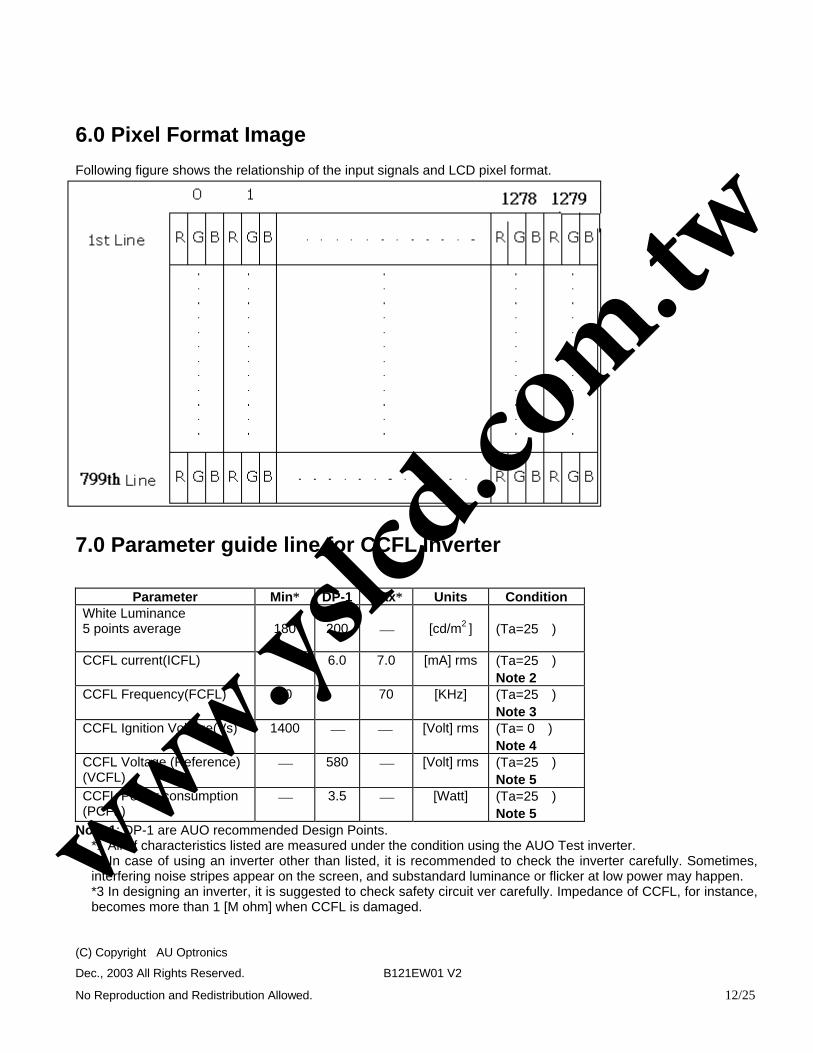
6.0 Pixel Format Image Following figure shows the relationship of the input signals and LCD pixel format.
7.0 Parameter guide line for CCFL Inverter
Parameter Min� DP-1 Max� Units Condition White Luminance 5 points average
180
200
[cd/m2 ]
(Ta=25℃)
CCFL current(ICFL) 6.0 7.0 [mA] rms (Ta=25℃) Note 2
CCFL Frequency(FCFL) 50 70 [KHz] (Ta=25℃) Note 3
CCFL Ignition Voltage(Vs) 1400 [Volt] rms (Ta= 0℃) Note 4
CCFL Voltage (Reference) (VCFL)
580 [Volt] rms (Ta=25℃) Note 5
CCFL Power consumption (PCFL)
3.5 [Watt] (Ta=25℃) Note 5
Note 1: DP-1 are AUO recommended Design Points. *1 All of characteristics listed are measured under the condition using the AUO Test inverter. *2 In case of using an inverter other than listed, it is recommended to check the inverter carefully. Sometimes, interfering noise stripes appear on the screen, and substandard luminance or flicker at low power may happen. *3 In designing an inverter, it is suggested to check safety circuit ver carefully. Impedance of CCFL, for instance, becomes more than 1 [M ohm] when CCFL is damaged.
(C) Copyright AU Optronics
Dec., 2003 All Rights Reserved. B121EW01 V2
No Reproduction and Redistribution Allowed. 12/25
www.yslcd.com.tw

*4 Generally, CCFL has some amount of delay time after applying start-up voltage. It is recommended to keep on applying start-up voltage for 1 [Sec] until discharge. *5 The CCFL inverter operating frequency must be carefully chosen so that no interfering noise stripes on the screen were induced. *6 Reducing CCFL current increases CCFL discharge voltage and generally increases CCFL discharge frequency. So all the parameters of an inverter should be carefully designed so as not to produce too much leakage current from high-voltage output of the inverter.
Note 2: It should be employed the inverter, which has “Duty Dimming”, if ICCFL is less than 4mA. Note 3: The CCFL inverter operating frequency should be carefully determined to avoid interference between
inverter and TFT LCD. Note 4: The inverter open voltage should be designed larger than the lamp starting voltage at T=0oC, otherwise
backlight may be blinking for a moment after turning on or not be able to turn on. The open voltage should be measured after ballast capacitor. If an inverter has shutdown function it should keep its open voltage. for longer than 1 second even if lamp connector is open.
Note 5: Calculator value for reference (ICFL×VCFL=PCFL)
8 Timing Control
(C) Copyright AU Optronics
Dec., 2003 All Rights Reserved. B121EW01 V2
No Reproduction and Redistribution Allowed. 13/25
www.yslcd.com.tw

88..11 TTiimmiinngg CChhaarraacctteerriissttiiccss This is the signal timing required at the input of the user connector . All of the interface signal timing should be satisfied with the following specifications .
Parameter Symbol Min. Typ. Max. Unit Condition
Clock frequency 1/ TClock 62 68.9 83 MHz
Period TV 803 816 864
Active TVD 800 800 800 Vertical Section
Blanking TVB 3 16 64
TLine
Period TH 1302 1408 1600
Active THD 1280 1280 1280Horizontal Section
Blanking THB 22 128 320
TClock
End-frame checking period tEF 2 TLine
DE checking period tDE 6400 TLine 8 Frames
88..22 TTiimmiinngg DDeeffiinniittiioonn
(C) Copyright AU Optronics
Dec., 2003 All Rights Reserved. B121EW01 V2
No Reproduction and Redistribution Allowed. 14/25
www.yslcd.com.tw

9.0 Power Consumption Input power specifications are as follows;
Symbol Parameter Min Typ Max Units Condition Module
VDD Logic/LCD Drive Voltage
3.0 3.3 3.6 [Volt] Load Capacitance 20uF
PDD VDD Power 1.6 [Watt] All Black Pattern PDD Max VDD Power max 1.7 [Watt] Max Pattern Note IDD IDD Current 400 mA 64 Grayscale Pattern IDD Max IDD Current max 420 mA Vertical stripe line Pattern
Note VDDrp Allowable
Logic/LCD Drive Ripple Voltage
500 [mV] p-p
VDDns Allowable Logic/LCD Drive Ripple Noise
100 [mV] p-p
Lamp ICFL CCFL current 3.0
(note 2)6.0 7.0 [mA]
rms (Ta=25℃)
VCFL CCFL Voltage (Reference)
580 [Volt] rms
(Ta=25℃)
PCFL CCFL Power consumption
3.5 [Watt] (Ta=25℃)
Total Power Consumption
5.0 Watt (w/o Inverter, All black pattern)@LCM circuit 1.5 Watt(typ.),B/L input 3.5 Watt(typ.)
Note 1 : VDD=3.3V Note 2 : If inverter with PWM mode that can define lamp min current is 2.5 mA.
(C) Copyright AU Optronics
Dec., 2003 All Rights Reserved. B121EW01 V2
No Reproduction and Redistribution Allowed. 15/25
www.yslcd.com.tw

10. Power ON/OFF Sequence VDD power and lamp on/off sequence is as follows. Interface signals are also shown in the chart. Signals from any system shall be Hi-Z state or low level when VDD is off.
Sequence of Power-on/off and signal-on/off
0.5ms≦T1≦10ms 0ms≦T2≦50ms 4T3T2
T1
0.1VDD
0.9VDD
0.1VDD
0.9VDD Power Supply VDD LVDS Interface Backlight On
Apply the lamp voltage within the LCD operating range. When the baLCD operation or the LCD turns off before the backlight turns off, thebecome abnormal.
(C) Copyright AU Optronics
Dec., 2003 All Rights Reserved. B121EW01 V2
No Reproduction and Redistribution Allowed.
www.yslcdco
.tw
Tm 0ms≦T3<50ms500ms≦T4 200ms≦T5 200ms≦T6
T5
VALIDT6.
cklight turns on before the display may momentarily16/25

11.0 Reliability /Safety Requirement
RReelliiaabbiilliittyy TTeesstt CCoonnddiittiioonnss
Items Required Conditions
Operating Life – High Temp. Temp.= +50°C, Dynamic. 250 Hours, Humidity 20%
Operating Life – Low Temp. Temp.= 0°C, Dynamic, 250 Hours, Humidity 20%
High Temp. Storage Life – Non-Operating Temp.= +65°C, Non-Operating, 250 Hours, Humidity 20%
Low Temp. Storage Life – Non-Operating Temp.= -25°C, Non-Operating, 250 Hours
High Temp & High Humidity Operating Life Temp.= +40°C, Dynamic, Humidity 95%(Non-Condensing), 250 Hours
Shock – Non-Operating 220g’s, 2.0 ms, Half Sine Wave ± 3 Axis ( +X, -X, +Y, -Y, +Z, -Z)3 Shocks per direction
Vibration – Non-Operating 1.5 Grms, 30 min/side, PSD Spectrum Break Points, 26 Hz G2/Hz=0.316, 50 Hz G2/Hz=0.007, 222 Hz G2/Hz=0.0018, 500Hz G2/Hz=0.0001
Temp. Cycle – Operating 0°C to+40°C, Ramp ≤20°C/min, Duration at Temp. = 30min, Test Cycles = 160
Temp. Cycle – Non-Operating -25°C to +65°C, Ramp ≤20°C/min, Duration at Temp. = 30min, Test Cycles = 50
CCFL Life : 10,000 hours minimum MTBF(Excluding the CCFL) : 50,000 hours with a confidence level 90%
1111..22 SSaaffeettyy UL60950
(C) Copyright AU Optronics
Dec., 2003 All Rights Reserved. B121EW01 V2
No Reproduction and Redistribution Allowed. 17/25
www.yslcd.com.tw
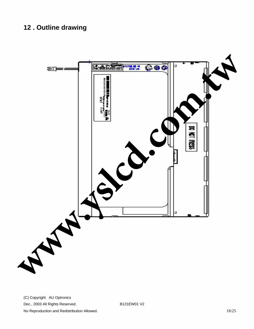
12 . Outline drawing
(C) Copyright AU Optronics
Dec., 2003 All Rights Reserved. B121EW01 V2
No Reproduction and Redistribution Allowed. 18/25
www.yslcd.com.tw

13 . EDID record (C) Copyright AU Optronics
Dec., 2003 All Rights Reserved. B121EW01 V2
No Reproduction and Redistribution Allowed. 19/25
www.yslcd.com.tw

(C) Copyright AU Optronics
Dec., 2003 All Rights Reserved. B121EW01 V2
No Reproduction and Redistribution Allowed. 20/25
B121EW01 V2 EDID Table Address FUNCTION Value Value Value Notes
HEX HEX BIN DEC
00 Header 00 00000000 0
01 FF 11111111 255
02 FF 11111111 255
03 FF 11111111 255
04 FF 11111111 255
05 FF 11111111 255
06 FF 11111111 255
07 00 00000000 0
08 EISA Manuf. Code LSB 06 00000110 6 ASCII Data String:B121EW01
09 Compressed ASCII AF 10101111 175 AUO
0A Product Code 01 00000001 1 01(12B01)
0B hex, LSB first 0C 00001100 12 12(12B01)
0C 32-bit ser # 00 00000000 0 unused
0D 00 00000000 0
0E 00 00000000 0
0F 00 00000000 0
10 Week of manufacture 01 00000001 1 Week 01
11 Year of manufacture 0E 00001110 14 14(2004-1990=14)
12 EDID Structure Ver. 01 00000001 1
13 EDID revision # 01 00000001 1
14 Video input definition 80 10000000 128 Digital Input
15 Max H image size 1A 00011010 26 26.112cm
16 Max V image size 10 00010000 16 16.32cm
17 Display Gamma 78 01111000 120 Gamma 2.2
18 Feature support 0A 00001010 10 no DPMS,Active off,RGB color
19 Red/green low bits A5 10100101 165
1A Blue/white low bits 50 01010000 80
1B Red x/ high bits 93 10010011 147 Rx=0.577
1C Red y 56 01010110 86 Ry=0.338
1D Green x 4F 01001111 79 Gx=0.310
1E Green y 8B 10001011 139 Gy=0.544
1F Blue x 28 00101000 40 Bx=0.158
www.yslcd.com.tw

20 Blue y 21 00100001 33 By=0.130
21 White x 50 01010000 80 Wx=0.313
22 White y 54 01010100 84 Wy=0.329
23 Established timing 1 00 00000000 0 unused
24 Established timing 2 00 00000000 0
25 Manufacturer's Timing 00 00000000 0
26 Standard timing #1 01 00000001 1 unused
27 01 00000001 1
28 Standard timing #2 01 00000001 1
29 01 00000001 1
2A Standard timing #3 01 00000001 1
2B 01 00000001 1
2C Standard timing #4 01 00000001 1
2D 01 00000001 1
2E Standard timing #5 01 00000001 1
2F 01 00000001 1
30 Standard timing #6 01 00000001 1
31 01 00000001 1
32 Standard timing #7 01 00000001 1
33 01 00000001 1
34 Standard timing #8 01 00000001 1
35 01 00000001 1
36 Pixel Clock/10,000 (LSB) 4C 01001100 76 Timing Descriptor #1
37 Pixel Clock/10,000 (MSB) 1D 00011101 29 1280x800 @65.27_mode:pixel clock=75.0MHz
38 Horiz. Active pixels(Lower 8 bits) 00 00000000 0 Horiz active=1280 pixels
39 Horiz.Blanking (Lower 8 bits) 80 10000000 128 Horiz blanking=128 pixels
3A Horiz. Active pixels:Horiz. Blanking (Upper4:4 bits) 50 01010000 80
3B 20 00100000 32 Vertcal active=800 lines
3C 10 00010000 16 Vertical blanking=16 lines
3D Vert. Active pixels:Vert. Blanking (Upper4:4 bits) 30 00110000 48
3E 15 00010101 21 Horiz sync. Offset=21 pixels
3F 20 00100000 32 Horiz sync. Pulse Width=32 pixels
40 Vert. Sync. Offset=xx lines, Sync Width=xx lines 44 01000100 68 Verti sync. Offset=4 lines,Sync Width=4 lines
41 Horz. Ver. Sync/Width (upper 2 bits) 00 00000000 0
42 Hori. Image size (Lower 8 bits) 05 00000101 5 Hori image size = 261.12 mm
43 Vert. Image size (Lower 8 bits) A3 10100011 163 Verti image size = 163.2mm
44 Hori. Image size : Vert. Image size (Upper 4 bits) 10 00010000 16
(C) Copyright AU Optronics
Dec., 2003 All Rights Reserved. B121EW01 V2
No Reproduction and Redistribution Allowed. 21/25
www.yslcd.com.tw

45 00 00000000 0 Horizontal Border = 0
46 00 00000000 0 Vertical Border = 0
47 18 00011000 24
48 Detailed timing/monitor 00 00000000 0 Apple definition, see the next sheet
49 descriptor #2 00 00000000 0
4A 00 00000000 0
4B 0F 00001111 15
4C Version 00 00000000 0
4D Value = HSPWmin /2 (pixel clks) 00 00000000 0 DE Mode
4E Value = HSPWmax /2 (pixel clks 00 00000000 0 DE Mode
4F Value = Thbpmin /2 (pixel clks) 00 00000000 0 DE Mode
50 Value = Thbpmax /2 (pixel clks) 00 00000000 0 DE Mode
51 Value = VSPWmin /2 (line pulses) 00 00000000 0 DE Mode
52 Value = VSPWmax /2 (line pulses) 00 00000000 0 DE Mode
53 Value = Tvbpmin /2 (line pulses 00 00000000 0 DE Mode
54 Value = Tvbpmax /2 (line pulses 00 00000000 0 DE Mode
55 Thpmin = value*2 + HA pixel clks (pixel clks) 0B 00001011 11 1302=Value*2+1280
56 Thpmax = value*2 + HA pixel clks (pixel clks) D2 11010010 210 1700=Value*2+1280
57 Tvpmin = value*2 + VA lines (line pulses) 02 00000010 2 803=Value*2+800
58 Tvpmax = value*2 + VA lines (line pulses) 10 00010000 16 832=Value*2+800
59 00 00000000 0
5A Detailed timing/monitor 00 00000000 0
5B descriptor #3 00 00000000 0
5C 00 00000000 0
5D FE 11111110 254
5E 00 00000000 0
5F Dell P/N 1st character 44 01000100 68 D
60 Dell P/N 2nd character 35 00110101 53 5
61 Dell P/N 3rd character 34 00110100 52 4
62 Dell P/N 4th character 30 00110000 48 0
63 Dell P/N 5th character 34 00110100 52 4
64 LCD Supplier EEDID Revision 00 00000000 0
65 Manufacturer P/N 42 01000010 66 B
66 Manufacturer P/N 31 00110001 49 1
67 Manufacturer P/N 32 00110010 50 2
68 Manufacturer P/N 31 00110001 49 1
(C) Copyright AU Optronics
Dec., 2003 All Rights Reserved. B121EW01 V2
No Reproduction and Redistribution Allowed. 22/25
www.yslcd.com.tw

69 Manufacturer P/N 45 01000101 69 E
6A Manufacturer P/N 57 01010111 87 W
6B Manufacturer P/N 31 00110001 49 1
6C Flag 00 00000000 0
6D Flag 00 00000000 0
6E Flag 00 00000000 0
6F Data type tag:ASCII string FE 11111110 254
70 Flag 00 00000000 0
71 SMBUS=15 nits E8 11101000 232
72 SMBUS=21 nits E0 11100000 224
73 SMBUS=30 nits C8 11001000 200
74 SMBUS=40 nits B0 10110000 176
75 SMBUS=60 nits 90 10010000 144
76 SMBUS=90 nits 70 01110000 112
77 SMBUS=140 nits 50 01010000 80
78 SMBUS=max nits(Typically = 00h) 00 00000000 0
79 01 00000001 1
7A 0A 00001010 10
7B 20 00100000 32
7C 20 00100000 32
7D 20 00100000 32
7E Extension Flag 00 00000000 0
7F Checksum A9 10101001 169
6457
6626 14. Label format
(C) Copyright AU Optronics
Dec., 2003 All Rights Reserved. B121EW01 V2
No Reproduction and Redistribution Allowed. 23/25
www.yslcd.com.tw

15.0 Packing dimension
20pcs LCD Module
12.1” LCD Module
Carton
Carton Label Position
ESD bag
(C) Copyright AU Optronics
Dec., 2003 All Rights Reserved. B121EW01 V2
No Reproduction and Redistribution Allowed. 24/25
www.yslcd.com.tw

(C) Copyright AU Optronics
Dec., 2003 All Rights Reserved. B121EW01 V2
No Reproduction and Redistribution Allowed. 25/25
www.yslcd.com.tw