xylem: enhancing vertical thermal conduction in 3d...
TRANSCRIPT

Xylem: Enhancing Vertical Thermal Conduction in 3DProcessor-Memory Stacks
Aditya Agrawal, Josep Torrellas, and Sachin Idgunji†
University of Illinois at Urbana-Champaign †Nvidia Corporationhttp://iacoma.cs.uiuc.edu
ABSTRACTIn upcoming architectures that stack processor and DRAM dies, tem-peratures are higher because of the increased transistor density andthe high inter-layer thermal resistance. However, past research hasunderestimated the extent of the thermal bottleneck. Recent experi-mental work shows that the Die-to-Die (D2D) layers hinder effectiveheat transfer, likely leading to the capping of core frequencies.
To address this problem, in this paper, we first show how to createpillars of high thermal conduction from the processor die to the heatsink. We do this by aligning and shorting dummy D2D µbumpswith thermal TSVs (TTSVs). This lowers processor temperaturessubstantially. We then improve application performance by boost-ing the processor frequency until we consume the available thermalheadroom. Finally, these aligned and shorted dummy µbump-TTSVsites create die regions of higher vertical thermal conduction. Hence,we propose to leverage them with three new architectural techniques:conductivity-aware thread placement, frequency boosting, and threadmigration. We evaluate our scheme, called Xylem, using simulationsof an 8-core processor at 2.4 GHz and 8 DRAM dies on top. µBump-TTSV alignment and shorting in a generic and in a customizedXylem design enable an average increase in processor frequency of400 MHz and 720 MHz, respectively, at an area overhead of 0.63%and 0.81%, and without exceeding acceptable temperatures. Thisimproves average application performance by 11% and 18%, respec-tively. Moreover, applying Xylem’s conductivity-aware techniquesenables further gains.
CCS CONCEPTS• Computer systems organization → Architectures; • Hardware→ 3D integrated circuits;
KEYWORDS3D chip, processor-memory integration, thermal management
ACM Reference format:Aditya Agrawal, Josep Torrellas, and Sachin Idgunji.2017. Xylem: EnhancingVertical Thermal Conduction in 3D Processor-Memory Stacks. In Proceed-ings of MICRO-50, Cambridge, MA,USA, October 14–18, 2017, 14 pages.https://doi.org/10.1145/3123939.3124547
Permission to make digital or hard copies of all or part of this work for personal orclassroom use is granted without fee provided that copies are not made or distributedfor profit or commercial advantage and that copies bear this notice and the full citationon the first page. Copyrights for components of this work owned by others than ACMmust be honored. Abstracting with credit is permitted. To copy otherwise, or republish,to post on servers or to redistribute to lists, requires prior specific permission and/or afee. Request permissions from [email protected], October 14–18, 2017, Cambridge, MA,USA© 2017 Association for Computing Machinery.ACM ISBN 978-1-4503-4952-9/17/10. . . $15.00https://doi.org/10.1145/3123939.3124547
1 INTRODUCTIONTechnology advances are about to enable further integration of com-puter architectures into chips that stack multiple memory and pro-cessor dies [2–4, 8, 34]. 3D stacking offers several benefits, such asa reduction in interconnect length and power, smaller form factors,and support for heterogeneous integration.
In these architectures, temperatures are higher than in conven-tional planar designs because of the increased transistor density, andbecause of the high inter-layer thermal resistance. In particular, theprocessor die is especially vulnerable, as it may be far from the heatsink — possibly at the bottom of the stack, so that processor power,ground, and I/O signals do not have to traverse the stack.
Stacking is made possible by Die-to-Die (D2D) connectionsand Through Silicon Vias (TSVs). D2D connections, also calledmicrobumps (or µbumps), exist between dies, while TSVs runacross the bulk silicon thickness of a die. TSVs carry electricalsignals and are built with materials of high thermal conductance.Some proposals complement them with Thermal TSVs (TTSVs)[12, 22, 23, 36, 54, 59], which are dummy TSVs for thermal con-duction only.
In this paper, we argue that past research has underestimated theextent of the thermal bottleneck in architectures that stack a highperformance multicore die and multiple DRAM dies. Specifically,it has assumed that the stacked layers have a relatively high ther-mal conductance [36], suggesting that TTSVs alone are effective atkeeping temperatures within acceptable values [12, 22, 23].
However, recent findings from IMEC [45, 46], Fujitsu [31, 43],IBM [9–11], and others [39, 40], shows that the material betweendies (or D2D layer) presents a high thermal resistance. It is ≈16xmore resistive than the bulk silicon, and ≈13x more resistive thanthe metal layers. In fact, the bulk silicon is one of the least thermallyresistive layers in the stack. As a result, while TTSVs running acrossthe bulk silicon (marginally) decrease the thermal resistance of thebulk silicon, they are not very effective overall. There are multipleD2D layers between the processor die and the heat sink, and theyhinder effective heat transfer. As a result, the temperature of theprocessor die remains high, which likely forces the capping of corefrequencies for reliability reasons.
To address this problem, in this paper, we show how to createpillars of high thermal conduction from the processor die at thebottom of the stack to the heat sink at the top. We do this by align-ing and shorting dummy D2D µbumps with TTSVs. This lowersprocessor temperatures substantially. We then improve applicationperformance by boosting the processor frequency until we consumethe available thermal headroom. Finally, these aligned and shorted

MICRO-50, October 14–18, 2017, Cambridge, MA,USA A. Agrawal et al.
dummy µbump-TTSV sites create die regions of higher vertical con-duction. Hence, we propose to leverage them with three new architec-tural techniques to further improve performance: conductivity-awarethread placement, frequency boosting, and thread migration.
We evaluate our proposal, called Xylem, using simulations ofa processor-memory stack. Our baseline is a Wide I/O compliantstack with an 8-core processor die at 2.4 GHz, and 8 DRAM dieson top. µBump-TTSV alignment and shorting in a generic and in acustomized Xylem design enable an average increase in processorfrequency of 400 MHz and 720 MHz, respectively, at an area over-head of 0.63% and 0.81%. This improves average application perfor-mance by 11% and 18%, respectively. Moreover, applying Xylem’sconductivity-aware techniques enables further, albeit smaller, gains.
This paper addresses issues from low-level technology to high-level system integration. Its main contributions are:• The observation that D2D layers are the thermal bottleneck in
processor-memory stacks. Hence, TTSVs alone are ineffective.• The creation of pillars of high thermal conduction through the
D2D layer by aligning and shorting dummy µbumps with TTSVs.• The observation that enhanced conduction through the D2D lay-
ers presents an architectural opportunity: the resulting thermalheadroom can be consumed by boosting processor frequency and,hence, improve application performance.
• Three new architectural techniques that leverage the enhancedconduction around the aligned and shorted dummy µbump-TTSVsites: conductivity-aware thread placement, frequency boosting,and thread migration.
2 BACKGROUND AND MOTIVATIONThe dies within a stack can be arranged in different configurations,such as: active layer of the dies facing each other (face-to-face or f2f),active layer of one facing the bulk of another (face-to-back or f2b),and bulk layer of the dies facing each other (back-to-back or b2b).For more than two homogeneous dies, such as a stack of DRAMdies, f2b is the preferred choice, and is the one we use. For multipleheterogeneous dies, such as memory and logic, the configuration isdictated by functionality, cost, performance, and thermal issues.
2.1 Through Silicon Vias (TSVs)TSVs are vertical interconnects that run across the thickness of thedie. There are several process flows for TSV fabrication, such as viafirst, via middle, frontside via-last, and backside via-last [5, 6, 29].In addition, TSVs can be made before or after bonding. With theexception of the frontside via-last process, a TSV is present only inthe silicon layer of a die, and not in the metal layers.
Ideally, we want a high TSV density (i.e., the number of TSVs ina given area). The density is determined by the TSV’s aspect ratioand the die thickness. A TSV’s aspect ratio is its height divided by itsdiameter, and is determined by manufacturing constraints and choiceof TSV metal. For example, tungsten (W) allows TSV aspect ratiosof about 30:1, while copper (Cu) is limited to no more than 10:1. Fora given die thickness, the TSV density is proportional to the squareof the aspect ratio; hence, high aspect ratios are preferred. For agiven aspect ratio, the density is inversely proportional to the squareof the die thickness. Hence, to attain high densities (and to aid TSVfabrication), dies are thinned down to a few tens of microns [3, 36].However, researchers have observed that die thinning reduces lateral
thermal spreading and worsens chip temperatures [16, 59]. Emma etal. [16] compare Cu and W TSVs in detail.
2.2 Die-to-Die Micro-Bumps (µBumps)µbumps provide the interconnection between the dies in the stack.They are like the C4 pads that connect a die to a board, but witha much finer pitch. Their pitch is larger than that of TSVs, andhence they determine the interconnect density between the dies. Themost widely-used implementation for a µbump is a Cu pillar with atin-silver solder.
µbumps can be electrical or dummy. Electrical µbumps providesignal connections between the dies. To facilitate more electricalconnections, electrical µbumps have fine diameters and pitch ofabout 17 µm and 50 µm, respectively [33]. Dummy µbumps exist,and are used for mechanical support and ease of stacking. They areelectrically grounded to prevent charge accumulation.
2.3 Thermal Effects in StacksStacking worsens on-die temperatures [3, 36, 59] because of theincreased transistor density and high inter-layer thermal resistance.The rate Q of heat flow (i.e., power) across a layer is proportionalto the thermal conductivity of the layer (λ ) and the temperaturedifference across the layer (δT ). Mathematically, Q ∝ λ ×δT . Ifthe power dissipated in a layer is constant, then a lower λ results ina higher temperature difference across the layer. Since the stack hasmultiple layers, the temperature differences add up, and the layerfarthest from the heat sink will be at the highest temperature.
In a stack, the layer between dies (or die-to-die (D2D) layer)has the lowest thermal conductance. This is because typical D2Dunderfills have a λ ≈ 0.5 W/m-K. In contrast, silicon has a λ ≈ 120W/m-K. Consequently, there is ongoing research on improving theD2D layer conductance, e.g., by using new underfills. An alternativeis to fill the D2D layer with dummy µbumps, after provisioningfor the electrical µbumps. Placing dummy µbumps has no area ormanufacturing overhead. Their location can be standardized in thefuture, similar to electrical µbumps.
While the thermal conductivity of a Cu pillar with the solder in aµbump is ≈ 40 W/m-K, the real thermal conductivity of a D2D layerfilled with dummy µbumps with a 25% density has been recentlymeasured, by IBM [9, 11] and others [39], to be only about 1.5W/m-K. The reason is that the D2D layer also includes several low-conductivity materials, like underfill/air, SiO2, and SiN. Detailedcross sections of the D2D layer can be found in [9, 11, 39]. Such alow thermal conductivity makes the multiple D2D layers the truethermal bottleneck in the stack.
Since TSVs are vertical metal interconnects with high thermalconduction, researchers have proposed to use dummy TSVs sim-ply for thermal conduction to reduce temperatures, as opposed tofor electrical conduction [12, 22, 23, 36, 54, 59]. These are calledThermal TSVs (TTSVs). TTSV improve the thermal conductionof only the bulk silicon layer. Hence, as we show later, they areineffective standalone at reducing the stack temperature. All TTSVsare electrically grounded to prevent charge accumulation.
2.4 Stacked Memory StandardsManufacturers and standards committees have proposed severalstacked memory architectures: Hybrid Memory Cube (HMC) [27]

Xylem: Enhancing Vertical Thermal Conduction MICRO-50, October 14–18, 2017, Cambridge, MA,USA
from Micron, and High Bandwidth Memory (HBM) [25], Wide I/O[62], and Wide I/O 2 [61] from JEDEC. HMC and HBM are 2.5Dmemory architectures with an optional die for controller operations.Wide I/O (prototyped by Samsung [33]) and Wide I/O 2 are true3D stacked architectures which can be connected to a processor diethrough TSVs. In this paper, we consider the thermal challenges in atrue 3D stack like Wide I/O plus a processor die.
Fig. 1 shows the Wide I/O organization. It supports 4 physicalchannels. Each one contains independent control, data, and clocksignals. Each memory die in the stack is called a slice, and has4 ranks (1 per channel). A stack of 4 slices results in 4 ranks perchannel and 16 overall. Each rank is divided into 4 banks, resultingin a total of 16 banks per slice. Current Wide I/O standards [61, 62]provide neither TTSVs nor dummy µbumps.
���������
����
���������
����
��������
����
����
�
����
�
����
�
����
�������
�������
(a) Slice organization.
�������
�������
������
������
�����
�����
(b) Stack organization.
Figure 1: Wide I/O organization (not to scale).
2.5 Shortcomings of Prior WorkRecent literature from IMEC, Fujitsu, IBM and others shows thatthe D2D layer is the thermal bottleneck in a stack. Specifically,Matsumoto et al. [39] and Colgan et al. at IBM [9, 11] independentlymeasure λD2D ≈ 1.5 W/m-K, and its thickness, t ≈ 20 µm, ona die-to-wafer and die-to-die bonding technology, respectively. Inaddition, Oprins et al. at IMEC [45, 46] state that the inter-diethermal resistance represents a significant part of the total resistancein a 3D stack, and measure a λD2D = 1.08 W/m-K on a wafer-to-wafer bonding process. Also, Nakamura et al. at Fujitsu [31, 43]point out that for thermal analysis of a 3D-stacked LSI, it is criticalto understand the heat flow through the microbumps.
Let us use Matsumoto’s and Colgan’s number. A layer’s thermalresistance per unit area is Rth = t/λ . Hence, the D2D layer’s Rth is ≈13.33 mm2-K/W. In comparison, the Rth of the bulk silicon layer in aprocessor die is ≈ 0.83, and that of the metal layers in the processordie is ≈ 1. This makes the D2D layer ≈ 16x more resistive than thebulk silicon, and ≈ 13x more resistive than the metal layers.
Unfortunately, prior CAD and architecture work has consistentlyunderestimated the D2D layer thermal resistance, either by assuminga high conductivity, a small thickness, or both. For example, [12]does not model the D2D layer at all. [36] uses a D2D thermalconductivity of λD2D ≈100 W/m-K, which is ≈ 65x higher thanwhat was measured. [22, 23] model the D2D layer thickness to beonly tD2D=0.7 µm, which is ≈ 20x lower than what was measured,and a λD2D that varies that from 1 to 100 W/m-K, which is upto ≈ 65x higher than what was measured. All this has resulted inunderestimating the thermal bottleneck effects of the D2D layer.
Prior proposals have focused on making the silicon layer of adie more conductive through the use of TTSVs. By underestimating
the D2D thermal bottleneck, their data shows that TTSVs alone areeffective for thermal management in 3D stacks. In this paper, byaccurately taking into account the D2D layer, we show that TTSVplacement alone is not effective at reducing the stack temperature.We need to combine it with a mechanism to reduce D2D layerthermal resistance.
3 MAIN STACK TRADE-OFFSWhen integrating DRAM and processor dies in a stack, the result-ing organization often depends on the specific characteristics of thetechnologies employed. This can be seen in recent research proto-types, such as Centip3De [15] and 3D-MAPS [32]. However, at ahigh level, there is a basic tradeoff between “processor-on-top” and“memory-on-top” organizations. These organizations are shown inFig. 2a and 2b, respectively.
��������
�������� ����������� �������
������������������������������
����������
�����������������
����������������� �����������
� !��������� � �������!��
� !���������
�������������"���#�$��
����������������%��� ���%��
�&��� �
���������������� ���������������
�����������������
����������������� � ����������
Figure 2: Two standard stack organizations.In both organizations, the top die is connected to the heat sink
and the Integrated Heat Spreader (IHS) using a Thermal InterfaceMaterial (TIM) [52]. Then, the different memory and processor diesare connected to each other through D2D connections and TSVs.
3.1 Processor on TopThe “processor-on-top” organization (Fig. 2a) has thermal advan-tages but significant manufacturing limitations. The advantages comefrom placing the die with most of the power dissipation closest to theheat sink. Also, the frontside metal layer of the processor die facesthe memory stack, so that the processor die does not need TSVs ordie thinning. The memory dies have TSVs and need die thinning.
The manufacturing difficulties result from the fact that a typicalprocessor die has close to a thousand pins, about half of which aredevoted to power and ground signals [16, 53]. In this organization,the memory dies have to provision TSVs to connect the proces-sor power, ground and I/O signals to the C4 pads. This is a largeoverhead. Moreover, different processors have different pin numberand location requirements. Therefore, the memory vendor eitherhas to grossly over provision TSVs to accommodate a wide varietyof processor dies, or manufacture custom dies for different proces-sor vendors. Neither approach is desirable. In addition, TSVs addresistance to the Power Delivery Network (PDN) [16, 53]. For acurrent-hungry processor die far away from the C4 pads, the IR dropacross the TSVs is a concern.

MICRO-50, October 14–18, 2017, Cambridge, MA,USA A. Agrawal et al.
������
������
���������
���������
������
��������
����
������
��������
��������
������������
������������
���������
���������
������
������
������
������
avgRth =13.33
R_small
R_small
R_small
R_big
R_big
R_big
Layer
(a)
Metal LayersBackside
D2DMicrobumpDummy
TTSV
TTSV
FrontsideMetal Layers
AirMicrobump
Air
(b)
Dummy
TTSV
TTSV
(c)
Rth=0.46
R_big
R_small
R_small
R_small
R_big
R_big
(d) (e)
Rth=0.22
Figure 3: Impact of dummy µbump-TTSV alignment and shorting.
3.2 Memory on TopThe “memory-on-top” organization (Fig. 2b) has some thermal chal-lenges, but does have clear manufacturing advantages. The thermalchallenges result from the fact that the heat generated in the proces-sor die has to traverse the many memory dies to reach the heat sink.Hence, the processor die will be at a significantly higher temperaturethan in planar organizations.
In this design, the frontside metal layer of the processor die isadjacent to the C4 pads. The main manufacturing advantage is thatthe high current-carrying power and ground signals, and the high-frequency I/O signals do not need TSVs [55]. In addition to simpli-fying the design, this avoids the IR drop issue mentioned above.
The memory stack in this configuration only contains TSVs asdefined by the various 3D memory stacking standards, such as WideI/O. The processor die only has to provision for the number andlocation of signals required for stack integration as given by thememory-stacking standards. Hence, the memory and processor diefloorplans are independent of each other. However, the processor diehas TSVs and requires thinning. Overall, given the manufacturingadvantages of the “memory-on-top” organization, we use it.
4 ENHANCING VERTICAL CONDUCTIONIn the “memory-on-top” organization, the processor (and memories)experience high temperatures. To avoid unsafe temperatures, thesesystems likely have to cap the frequency of the processor, in turnhurting performance.
To solve this problem, we propose to create pillars of high thermalconduction from the processor die to the heat sink at the top. For that,we need to focus on the thermal bottleneck, which is the D2D layers.In the following, we present the Xylem solution, which consists ofaligning and shorting dummy D2D µbumps and TTSVs.
4.1 µBump-TTSV Alignment and Shorting4.1.1 Summary of the Problem. Fig. 4 shows the interface be-
tween two f2b DRAM dies [44]. From top to bottom, we see theface side of a die, a D2D layer, and the back side of another die.The upper die shows the bulk silicon layer, which has the activedevices and electrical TSVs, and the frontside metal layers. The lat-ter contain metal routing layers (M1 to Mn) separated by dielectricmaterials with low thermal conductance. The D2D layer consists ofa layer with µbumps separated by air or underfill, and the backsidemetal layers of the lower die — which typically have 0-2 layers ofmetal routing (BM1 to BM2) separated by dielectric materials withlow thermal conductance. On the left side, a TSV in the lower die isconnected through the backside metal layers to an electrical µbumpand then through the frontside metal layers to devices in the upperdie.
���
����
���
��
�������������� ��� ��������� ���������
���� �� �� ����������������
����
�����
������
�����
����������������� � ������������� ������
����
�����
����
Figure 4: f2b DRAM die interface (not to scale).
In the figure, we have added two TTSVs and two dummy µbumps,shown in stripes. As the figure shows, the TTSVs typically terminateat the bulk silicon layers. In particular, they avoid the frontsidemetal layers because they would cause routing congestion in thealready busy metal layers.1 TTSVs are generally not aligned withthe µbumps.
As indicated in Section 2.5, data from Colgan et al. at IBM [9, 11]and Matsumoto et al. [39] shows that the D2D layer has a high Rthof ≈13.33 mm2-K/W. This is the result of a sizable thickness andof a low thermal conductivity λ . The multiple D2D layers are thethermal bottleneck in the stack.
4.1.2 Proposed Solution. Our approach is to align dummy µbumpsin the D2D layer with TTSVs in the back side of the die and shortthem. To see how, consider Fig. 3a, which shows two identicalDRAM dies connected f2b. There are two TTSVs that are aligned,but are separated by a D2D layer and the frontside metal layers ofthe upper die. We align the TTSVs with a dummy µbump (Fig. 3b)and then, using a backside metal via, short the dummy µbump withthe lower-die TTSV (Fig. 3c).
Ideally, we would also want to short the upper-die TTSV with theµbump. However, the frontside metal layers carry many electricalsignals, and using a frontside metal via [10] may or may not bepossible, and may cause routing congestion. In addition, as shown inFig. 3c, the Rth of the frontside metal layers is only 0.22 mm2-K/W.This number is obtained with d=2 µm and λ=9 W/m-K [3]. This issmall compared to the Rth of the original D2D layer.
With this approach, we have created a path of low thermal re-sistance from the lower-die TTSV through the D2D layer, whichdrains the heat. Specifically, given that the λ of the TTSV’s Cu is
1The exception is when TSVs are built using the more costly frontside via lastprocess, as in Black et al. [3].

Xylem: Enhancing Vertical Thermal Conduction MICRO-50, October 14–18, 2017, Cambridge, MA,USA
400 W/m-K [3], the λ of the µbump is 40 W/m-K [39], and theµbump’s thickness is 18µm, we compute the Rth of the D2D layerat this location as Rth_bump + Rth_short= 18µm / 40W/m-K + 2µm /400W/m-K = 0.46 mm2-K/W. This is a local Rth that is ≈30x lowerthan the average Rth of 13.33.
Pictorially, we have moved from an environment with thermalresistances like Fig. 3d to one like Fig. 3e. Fig. 3d represents Fig. 3a.We have a large thermal resistance (average of the D2D layer) con-necting two small thermal resistances (the TTSVs), all in parallelwith a small resistance (the µbump) connecting two relatively largerresistances (the silicon of the dies). On the other hand, Fig. 3e repre-sents Fig. 3c. We have connected all three small resistances in series.A trivial calculation of the equivalent resistance shows that the heathas now a low-resistance path.
Electrical TSVs also contribute to thermal conduction becausethey are connected to µbumps. However, their contribution is limited.The reason is that the placement of electrical TSVs in the chip isdictated by stacking standards, and is oblivious to hotspots. Forexample, Wide I/O clusters all 1,200 TSVs in the center of thememory die, together with the electrical µbumps (Fig. 1).
4.2 Placing TTSVsWe now consider how to place the TTSVs in the dies. Then, align-ing dummy µbumps to these TTSV will be easy because dummyµbumps are plentiful. Ideally, we want the TTSV diameter to be thesame as the µbump diameter, to facilitate maximum heat flow.
We build on top of a stack that follows the Wide I/O organization(Fig. 1). Each die has a TSV bus in its center with 1,200 TSVsmeant for electrical connections, together with the electrical µbumps.One such die is shown in Fig. 5a. These TSVs also aid in thermalconduction.
����
�������
�����
(a) Baseline.
����
���� �������
�����
(b) Bank Surround.
����
���� �������
�����
(c) Bank Surround Enhanced.
����
���� �������
�����
(d) Iso Count.
Figure 5: Xylem schemes.
To place TTSVs, we need to abide by the DRAM die floorplanand physical constraints. First, we place the TTSVs in the peripheral
logic, to avoid disrupting the regular nature of the banks. Second,to avoid the TSV’s lateral thermal blockage [7], we distribute theTTSVs, instead of aggregating them into a large TTSV farm. Finally,since TSV fabrication affects transistor performance nearby [1], wemaintain a Keep Out Zone (KOZ) around each TTSV. Note that theperipheral logic contains row/column decoders, charge pumps, I/Ologic, and temperature sensors. Hence, placing TTSVs has an areaoverhead.
Based on these constraints, we propose two simple TTSV place-ments, namely one generic and one custom. Ideally, TTSV place-ment should be generic. Memory manufacturers should not makeassumptions about other layers of the stack, such as the location ofthe hotspots in the processor die. Our generic placement is calledBank Surround (bank) and is shown in Fig. 5b. It places the TTSVsin the peripheral logic at the vertices of each bank. Note that theperipheral logic area that runs horizontally across the die centeris wider because of the Wide I/O TSV bus. Hence, we place twoTTSVs at each point in the center stripe, instead of one everywhereelse. The total number of TTSVs in the die is 28.
If we know the hotspots in the processor, we can devise a moreeffective, custom TTSV placement strategy. In this paper, we usethe processor die floorplan shown in Fig. 6. This is a typical layoutfor commercial processors [20, 30, 56–58, 60], where the cores areon the outside and the Last-Level Cache (LLC) in the center. Thislayout separates the hot spots, which are the cores. The figure showsthat the Wide I/O memory controllers and part of the TSV bus arein the logic layer. This is a layer in between the bulk silicon and themetal layers; it was not shown in Fig. 2 for simplicity.
��
���
���
��
�����
���
���
��
����
���
���
��
�����
���
���
��
�����
�� �� ��
���
���
����
���
���
�����
���
���
�����
���
���
�����
���������� ���� ��� �������� �����������
� ����������������� ��������������������
����������������� ���� ����!������ ��������
Figure 6: Processor die floorplan.Knowing the location of the cores, we add 8 additional TTSVs
close to the cores. The result is the Bank Surround Enhanced (banke)scheme of Fig. 5c. The total number of TTSVs is now 36. In effect,we have co-designed the memory and processor dies.
Finally, to perform experiments at a constant number of TTSVs,we take Bank Surround Enhanced and remove the 8 TTSVs fromthe peripheral logic area running horizontally across the die center.The resulting scheme, shown in Fig. 5d, has the same TTSV countas Bank Surround. We call it Iso Count.
5 TRADING THERMALS & PERFORMANCEThe alignment and shorting of dummy µbumps and TTSVs createspillars of high thermal conduction from the processor die to the heatsink. We now show how we translate this feature into performanceimprovements.

MICRO-50, October 14–18, 2017, Cambridge, MA,USA A. Agrawal et al.
5.1 Boosting Processor FrequencyAn increase in the thermal conduction from the processor die to theheat sink results in a reduction in the temperature of the processor.Consequently, we propose to increase the processor’s frequency andvoltage until we consume the thermal headroom enabled. The re-sult is higher application performance. For this, we use the DVFSinfrastructure available in commercial processors [51]. DVFS infras-tructure uses hardware and firmware, and is low overhead.
With Xylem, the manufacturer can rate the processor to workat a higher frequency for the same temperature limit. This opti-mization shows that, in a stacked architecture, there is a direct linkbetween temperature and performance. Since these architectures areso thermally-limited, techniques like Xylem that reduce the temper-ature can improve performance substantially.
5.2 Conductivity (λ ) Aware TechniquesThe presence of pillars of high thermal conduction induces spatialheterogeneity in the processor die in its ability to dissipate heat.We refer to the sites with aligned and shorted µbump-TTSVs ashigh vertical conductivity (λ ) sites. The die areas close to thesesites dissipate heat more easily than areas far from them. Hence, wepropose λ -aware optimizations, which leverage the higher thermalconduction around these sites. As examples, we propose λ -awarethread placement, λ -aware frequency boosting, and λ -aware threadmigration.
λ -aware techniques can be applied when there is obvious het-erogeneity in vertical conduction. An example is when two dies ofdifferent materials are placed side by side, both on top of the pro-cessor die. In this case, one of the two same-level dies may enablehigher vertical λ than the other die. λ -aware techniques can leveragethis heterogeneity.
Even regular layouts such as bank and banke present thermalheterogeneity and can be leveraged by λ -aware techniques. Specifi-cally, the inner cores in Figure 6 (cores 2, 3, 6, and 7) have a smalleraverage distance to the high vertical λ sites compared to the outercores (cores 1, 4, 5, and 8). This is the effect that we exploit in theλ -aware techniques.
5.2.1 λ -Aware Thread Placement. The idea is to place the mostthermally demanding threads on cores that are, on average, closer tothe high vertical λ sites. Typically, the most thermally demandingthreads are compute intensive. Our proposal is to place these threadson the inner cores, and the memory intensive threads on the outercores. The result is a higher reduction in temperature than with arandom placement and, hence, the ability to enable a higher increasein processor frequency. Note that all cores in the chip have the samedistance to the on-chip coherence bus and, hence, to the Wide I/Omemory controllers.
5.2.2 λ -Aware Frequency Boosting. Cores that are on averagefarther from the high vertical λ sites reach the temperature limitbefore cores that are on average closer to them. Consequently, wepropose λ -aware frequency boosting. The idea is to boost the fre-quency of the cores that are closer to these sites more than the others.In our processor die, we boost the frequency of the inner cores morethan that of the outer cores, so that all cores reach the maximumtemperature. With this technique, we improve performance.
5.2.3 λ -Aware Thread Migration. If we have fewer threads thancores, we may want to run a thread at high frequency on a core untilthe maximum temperature is attained, and then migrate the threadto an idle, cool core [21, 24]. This is repeated until the programterminates. In general, cores that are on average closer to the highvertical λ sites will take longer to reach the maximum temperaturethan the others. Consequently, in λ -aware thread migration, wepropose to migrate a thread between cores that are on average closerto the high vertical λ sites, rather than between those on averagefarther, or between random cores. We will need fewer migrations tocomplete the program or, if we migrate at the same frequency, wewill keep the cores at a lower average temperature. In our processordie, we migrate threads between the inner cores rather than betweenouter cores to keep a lower average temperature.
Note that λ -aware techniques are different from past thermal-aware techniques [63, 64]. Past work assumed that all cores arehomogeneous. However, in Xylem, the cores are heterogeneous dueto different conductivities. Our techniques exploit this heterogeneity.For example, consider a thread-to-core assignment decision. If twocores are at about the same temperature, past work will pick a corerandomly. However, Xylem will pick the core with a higher λ .
6 THERMAL MODELING AND SETUP6.1 Thermal ModelingWe model a “memory-on-top” processor-memory stack, with 8DRAM dies on top of a multicore processor die. As shown in Fig.2b,the stack is composed of many distinct layers: active heat sink, In-tegrated Heat Spreader (IHS), Thermal Interface Material (TIM),DRAM silicon, DRAM metal, D2D, processor silicon, and processormetal. Some layers occur multiple times in the stack. TTSVs arepresent only in the DRAM silicon and processor silicon layers.
Some layers are heterogeneous, e.g., due to the presence of TSVsand TTSVs. We model each layer as being composed of many rect-angular blocks. For numerical stability, it is desirable for the blocksto have a squarish aspect ratio. Different blocks within the samelayer may have different λ . Note, however, that while the floorplanis specified in these rectangular blocks, the thermal simulation isperformed in grid mode for higher accuracy.
The λ of an area with two materials A and B, with conductivitiesλA and λB, and fractional area occupancies ρA and ρB, such thatρA +ρB = 1, is [41]: λ = ρA ×λA +ρB ×λB. For example, a TSVbus is composed of 25% Cu with λ=400 W/m-K and 75% Si withλ=120 W/m-K. Hence, its effective λ = 0.25×400 + 0.75×120 =190 W/m-K.
Silicon and Frontside Metal. For accurate thermal analysis, thesilicon layer and the metal layer of a die are modeled as two separatelayers [3, 36]. We model the metal layer to also include the activesilicon (or logic layer) because it is difficult to separate the powerconsumed by transistors and by wires. The metal routing layers (typ-ically Al for memory and Cu for processor) together with dielectricshave a different λ than silicon. Since Al has a lower λ than Cu, theλ of the metal layer of a memory die is lower than that of the metallayer of the processor die [3]. The block boundaries in this layer arethe architectural block boundaries — e.g., fetch, issue, RF, or ALU.

Xylem: Enhancing Vertical Thermal Conduction MICRO-50, October 14–18, 2017, Cambridge, MA,USA
TSVs and TTSVs. We use Cu as the material for electrical TSVsand TTSVs because it has a high electrical and thermal conductivity.From ITRS [28], the electrical TSV size is 10 µm. Since the aspectratio of Cu is limited to 10:1 [16], we use a die thickness of 100µm for all the dies in the stack. We use a KOZ of 10 µm in boththe X and Y dimensions. This results in an X and Y TSV pitch of20 µm, and fractional area occupancies of 0.25 and 0.75 for the Cuand Si, respectively. The 1200 electrical TSVs are modeled using 48blocks of 5×5 TSVs each. Each block is 100µm×100µm, and hasan effective λ of 190 W/m-K. Each TTSV is modeled as a singleblock of 100µm×100µm with a λ of 400 W/m-K. It has a KOZ of10 µm in both the X and Y dimensions.
D2D Layer. The D2D layer contains µbumps and backside metallayers, and is modeled as discussed in Sec. 4.1. The 1200 electricalµbumps in the center of the die are also organized in 48 blocksof 5×5 µbumps each, with a total effective λ of 1.5 W/m-K. Eachdummy µbump has a size of 100µm×100µm, and a λ of 40 W/m-K.Dummy µbumps have a 25% occupancy.
TTSVs and dummy µbumps are thicker than electrical TSVsand µbumps. This is to facilitate maximum heat transfer. One canimagine a foundry to provide a library of TSVs and µbumps ofdifferent sizes. Alternatively, an array of skinny TSVs and smallerµbumps can be used to mimic a thick TTSV and a thick dummyµbump.
Table 1 shows the dimensions and λ of the layers in the stack.These values are obtained from various sources [3, 16, 26, 36].
Layer Dimensions Thermal Conductivity λ
(W/m-K)
Heat Sink 6.0x6.0x0.7 cm3 400IHS 3.0x3.0x0.1 cm3 400TIM 50 µm 5DRAM Silicon 100 µm 120 (Si); 400 (TSV);
190 (TSV bus)DRAM Metal 2 µm 9D2D 20 µm 1.5 (µbump = 40)Proc Silicon 100 µm 120 (Si); 400 (TSV);
190 (TSV bus)Proc Metal 12 µm 12
Table 1: Dimensions and thermal parameters.
Table 2 shows the different Xylem schemes evaluated. For eachscheme, we list the name used in the evaluation and the number ofTTSVs per die. The table includes the four schemes of Fig. 5 plusone additional one, called prior. Prior is similar to banke except thatdummy µbumps and TTSVs are neither aligned nor shorted and,hence, there is no good conduction path through the D2D layers.Prior mimics the prior proposals, which place TTSVs near hotspotsbut ignore the impact of the D2D layers [12, 22, 23].
Xylem Scheme Name #TTSVs per Chip
Baseline (Wide I/O) base 0Bank Surround bank 28Bank Surround Enhanced banke 36Iso Count isoCount 28Prior proposals prior 36
Table 2: Xylem schemes evaluated.
6.2 ArchitectureThe architecture is an 8-core chip multiprocessor under a stack of 8DRAM dies. We use 32 nm technology. Each core is 4 issue and outof order. It has private L1 instruction and data caches, and a privateL2 unified cache. A bus-based snoopy MESI protocol maintainscoherence between the L2s. Each of the 8 DRAM dies has 4 Gb(512 MB) of memory, resulting in 4 GB of memory for the stack.
The DRAM stack organization follows Wide I/O [62]. The WideI/O standard supports a modest bandwidth of about 12.8 GB/s, whileWide I/O 2 [61] supports a bandwidth of about 51.2 GB/s. Hence,we use the Wide I/O stack organization, but use a data rate of 51.2GB/s. Note that the problems and solution proposed in this paper aregenerally applicable to any processor-memory stack.
The frequency of our architecture can change between 2.4 GHz(default) and 3.5 GHz in 100 MHz steps. At 2.4 GHz, the powerconsumed by the base system is 8-24 W in the processor die and2-4.5 W in the memory dies. Both the processor and the DRAMdies have a similar area of ≈64mm2 and a similar aspect ratio. Thissimplifies the analysis. If processor and DRAM die areas are differ-ent, we need to perform a slightly more involved thermal analysis,but the methodology is largely the same. We use a maximum safetemperature for the processor of Tj,max=100 ◦C, and a maximum forthe DRAM of 95 ◦C, which is within the extended range allowed byJEDEC [14]. The architectural parameters are summarized in Table3. We have broadly validated our power estimations with publishednumbers from Intel’s Xeon E3-1260L.
Processor Parameters
Multicore chip 32nm, eight 4-issue OoO, 2.4-3.5 GHzInst. L1 cache 32 KB, 2 way, 2 cycles Round Trip (RT)Data L1 cache 32 KB, 2 way, WT, 2 cycles RTL2 cache 256 KB, 8 way, WB, private, 10 cycles RTCache Line; Network 64 bytes; 512 bit busCoherence Bus-based snoopy MESI protocol at L2DRAM access ≈ 100 cycles RT (idle)Max. temperature Processor: T j,max=100◦C; DRAM=95◦C
Stack DRAM Parameters
Dies; Channels 8; 4Ranks/die; Banks/rank 4 (1 per channel); 4Capacity 4 Gb/die = 4 GB total in stackI/O freq.; Data rate 800 MHz; DDR# of memory controllers 4 Wide I/O DRAM controllers
Table 3: Architectural parameters.
6.3 Tools and ApplicationsWe use the SESC [49] cycle-level simulator to model the architecture.We obtain the dynamic and leakage energy of the processor die fromMcPAT [35]. The timing and energy of the DRAM dies is modeledwith DRAMSim2 [50]. We also use McPAT to estimate the area ofthe blocks within the processor die. The floorplan for each layer inthe 3D stack is obtained using ArchFP [17]. Fig. 6 shows the high-level floorplan of the processor die that we use in the evaluation. Weensure that known hotspots in the processor die such as FPUs arespatially separated from each other.
To model the thermal effects in a stacked architecture, we useHotSpot’s extension in [41]. The original HotSpot [26] models 3D-stacked architectures, but only allows homogeneous layers. The
MICRO-50, October 14–18, 2017, Cambridge, MA,USA A. Agrawal et al.
60 °C
70 °C
80 °C
90 °C
100 °C
110 °C
120 °C
130 °C
base
bank
banke
prio
r
base
bank
banke
prio
r
base
bank
banke
prio
r
base
bank
banke
prio
r
base
bank
banke
prio
r
base
bank
banke
prio
r
base
bank
banke
prio
r
base
bank
banke
prio
r
base
bank
banke
prio
r
base
bank
banke
prio
r
base
bank
banke
prio
r
base
bank
banke
prio
r
base
bank
banke
prio
r
base
bank
banke
prio
r
base
bank
banke
prio
r
base
bank
banke
prio
r
base
bank
banke
prio
r
2.4 GHz2.8 GHz3.2 GHz3.5 GHz
SPMGLU (NAS)ISFTCGBTBlack.Fluid.RaytraceRadiosityFMMBarnesRadixLUCholeskyFFT
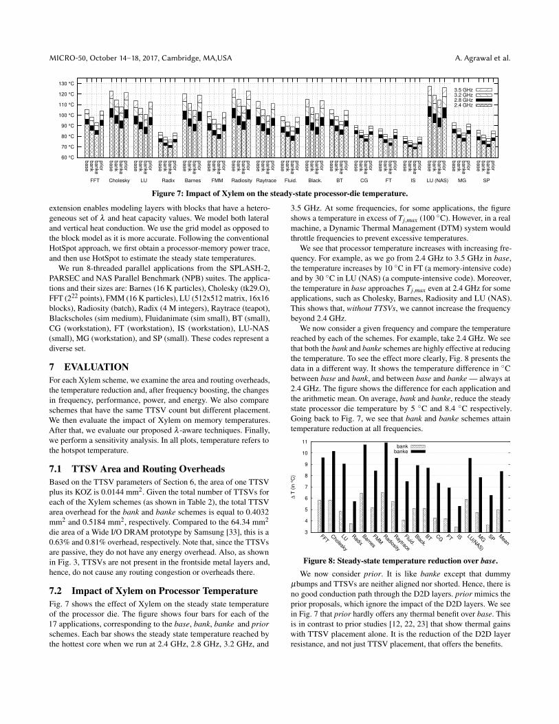
Figure 7: Impact of Xylem on the steady-state processor-die temperature.
extension enables modeling layers with blocks that have a hetero-geneous set of λ and heat capacity values. We model both lateraland vertical heat conduction. We use the grid model as opposed tothe block model as it is more accurate. Following the conventionalHotSpot approach, we first obtain a processor-memory power trace,and then use HotSpot to estimate the steady state temperatures.
We run 8-threaded parallel applications from the SPLASH-2,PARSEC and NAS Parallel Benchmark (NPB) suites. The applica-tions and their sizes are: Barnes (16 K particles), Cholesky (tk29.O),FFT (222 points), FMM (16 K particles), LU (512x512 matrix, 16x16blocks), Radiosity (batch), Radix (4 M integers), Raytrace (teapot),Blackscholes (sim medium), Fluidanimate (sim small), BT (small),CG (workstation), FT (workstation), IS (workstation), LU-NAS(small), MG (workstation), and SP (small). These codes represent adiverse set.
7 EVALUATIONFor each Xylem scheme, we examine the area and routing overheads,the temperature reduction and, after frequency boosting, the changesin frequency, performance, power, and energy. We also compareschemes that have the same TTSV count but different placement.We then evaluate the impact of Xylem on memory temperatures.After that, we evaluate our proposed λ -aware techniques. Finally,we perform a sensitivity analysis. In all plots, temperature refers tothe hotspot temperature.
7.1 TTSV Area and Routing OverheadsBased on the TTSV parameters of Section 6, the area of one TTSVplus its KOZ is 0.0144 mm2. Given the total number of TTSVs foreach of the Xylem schemes (as shown in Table 2), the total TTSVarea overhead for the bank and banke schemes is equal to 0.4032mm2 and 0.5184 mm2, respectively. Compared to the 64.34 mm2
die area of a Wide I/O DRAM prototype by Samsung [33], this is a0.63% and 0.81% overhead, respectively. Note that, since the TTSVsare passive, they do not have any energy overhead. Also, as shownin Fig. 3, TTSVs are not present in the frontside metal layers and,hence, do not cause any routing congestion or overheads there.
7.2 Impact of Xylem on Processor TemperatureFig. 7 shows the effect of Xylem on the steady state temperatureof the processor die. The figure shows four bars for each of the17 applications, corresponding to the base, bank, banke and priorschemes. Each bar shows the steady state temperature reached bythe hottest core when we run at 2.4 GHz, 2.8 GHz, 3.2 GHz, and
3.5 GHz. At some frequencies, for some applications, the figureshows a temperature in excess of Tj,max (100 ◦C). However, in a realmachine, a Dynamic Thermal Management (DTM) system wouldthrottle frequencies to prevent excessive temperatures.
We see that processor temperature increases with increasing fre-quency. For example, as we go from 2.4 GHz to 3.5 GHz in base,the temperature increases by 10 ◦C in FT (a memory-intensive code)and by 30 ◦C in LU (NAS) (a compute-intensive code). Moreover,the temperature in base approaches Tj,max even at 2.4 GHz for someapplications, such as Cholesky, Barnes, Radiosity and LU (NAS).This shows that, without TTSVs, we cannot increase the frequencybeyond 2.4 GHz.
We now consider a given frequency and compare the temperaturereached by each of the schemes. For example, take 2.4 GHz. We seethat both the bank and banke schemes are highly effective at reducingthe temperature. To see the effect more clearly, Fig. 8 presents thedata in a different way. It shows the temperature difference in ◦Cbetween base and bank, and between base and banke — always at2.4 GHz. The figure shows the difference for each application andthe arithmetic mean. On average, bank and banke, reduce the steadystate processor die temperature by 5 ◦C and 8.4 ◦C respectively.Going back to Fig. 7, we see that bank and banke schemes attaintemperature reduction at all frequencies.
3
4
5
6
7
8
9
10
11
FFTCholesky
LU Radix
Barnes
FMM
Radiosity
Raytrace
Fluid.
Black.
BT CG
FT IS LU(N
AS)
MG
SP Mean
∆ T
(in
°C
)
bankbanke
Figure 8: Steady-state temperature reduction over base.We now consider prior. It is like banke except that dummy
µbumps and TTSVs are neither aligned nor shorted. Hence, there isno good conduction path through the D2D layers. prior mimics theprior proposals, which ignore the impact of the D2D layers. We seein Fig. 7 that prior hardly offers any thermal benefit over base. Thisis in contrast to prior studies [12, 22, 23] that show thermal gainswith TTSV placement alone. It is the reduction of the D2D layerresistance, and not just TTSV placement, that offers the benefits.
Xylem: Enhancing Vertical Thermal Conduction MICRO-50, October 14–18, 2017, Cambridge, MA,USA
7.3 Effect of Temperature ReductionFig. 7 also shows that, at a fixed processor temperature, Xylem canrun the system at higher frequencies. This can be seen by drawingan imaginary horizontal line and seeing that, as we go from baseto bank and banke, we are substantially increasing the frequency ofoperation. This is one of the opportunities we exploit: improvingthermal conduction, then boosting the frequency, for constant steadystate temperature.
In this section, for each application, we choose the temperatureof the base scheme at 2.4 GHz as a reference. Then, for the sameapplication, for bank and banke, we find the frequency at which theprocessor temperature is closest to the reference without exceedingit. In the following, we analyze the resulting increase in systemfrequency and application performance, and the change in systempower and energy.
7.3.1 System Frequency Increase. Fig. 9 shows the increase insystem frequency enabled by the bank and banke schemes overbase. Recall that, for each application, we keep the steady statetemperature equal to the one in the base scheme at 2.4 GHz. Thefigure shows bars for each application and the arithmetic mean.We see that, on average for all the applications, bank boosts thefrequency by about 400 MHz, and banke boosts it by 720 MHz.These are substantial increases, which we argue justify the designeffort and area cost of Xylem. These large increases are the result ofbase being highly frequency-throttled. Indeed, the cores are designedto run at 3.5 GHz, but thermal constraints in base force them to runat 2.4 GHz.
200
400
600
800
1000
FFTCholesky
LU Radix
Barnes
FMM
Radiosity
Raytrace
Fluid.
Black.
BT CG
FT IS LU(N
AS)
MG
SP Mean
∆ F
req
ue
ncy (
in M
Hz)
bankbanke
Figure 9: System frequency increase over base.
7.3.2 Application Performance Increase. Fig. 10 shows the appli-cation performance increase over the base scheme as a result of thefrequency boosting enabled by the bank and banke schemes. The fig-ure shows bars for each application and for the geometric mean. Wecan see that, on average, bank boosts the application performance by11%, and banke boosts it by 18%. These are also large performanceincreases.
7.3.3 System Power and Energy Change. In our base system, itcan be shown that the processor die consumes 8-24 W and the 8-diememory stack 2-4.5 W. Since Xylem enables frequency increases,the power and energy consumed by the processor-memory stackwill change. Fig. 11 shows the increase in the power consumed bythe stack in bank and banke over base. The figure is organized asbefore, with the last bars showing the geometric mean. We see that,on average, bank and banke increase the power consumption by
5
10
15
20
25
30
FFTCholesky
LU Radix
Barnes
FMM
Radiosity
Raytrace
Fluid.
Black.
BT CG
FT IS LU(N
AS)
MG
SP Mean
Perf
orm
ance G
ain
(in
%)
bankbanke
Figure 10: Application performance increase over base.
12% and 22%, respectively. The heat sink is able to dissipate thisadditional power while maintaining the same temperature as base.
6
8
10
12
14
16
18
20
22
24
26
28
FFTCholesky
LU Radix
Barnes
FMM
Radiosity
Raytrace
Fluid.
Black.
BT CG
FT IS LU(N
AS)
MG
SP Mean
Po
we
r In
cre
ase
(in
%)
bankbanke
Figure 11: Stack power increase over base.
Fig. 12 shows the change in energy consumed by the stack inthe bank and banke schemes over the base scheme. The figure isorganized as before. As shown in the geometric mean bars, theapplications end up consuming about the same energy on average.This is because of race-to-halt effects in some applications.
-15
-10
-5
0
5
10
FFTCholesky
LU Radix
Barnes
FMM
Radiosity
Raytrace
Fluid.
Black.
BT CG
FT IS LU(N
AS)
MG
SP Mean
Energ
y C
hange (
in %
)
bankbanke
Figure 12: Stack energy change over base.
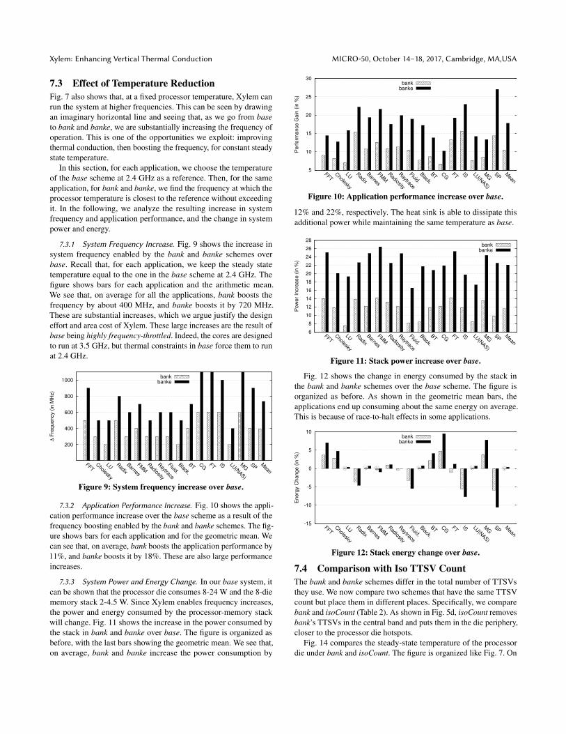
7.4 Comparison with Iso TTSV CountThe bank and banke schemes differ in the total number of TTSVsthey use. We now compare two schemes that have the same TTSVcount but place them in different places. Specifically, we comparebank and isoCount (Table 2). As shown in Fig. 5d, isoCount removesbank’s TTSVs in the central band and puts them in the die periphery,closer to the processor die hotspots.
Fig. 14 compares the steady-state temperature of the processordie under bank and isoCount. The figure is organized like Fig. 7. On

MICRO-50, October 14–18, 2017, Cambridge, MA,USA A. Agrawal et al.
60 °C
70 °C
80 °C
90 °C
100 °C
110 °C
120 °C
base
bank
banke
prio
r
base
bank
banke
prio
r
base
bank
banke
prio
r
base
bank
banke
prio
r
base
bank
banke
prio
r
base
bank
banke
prio
r
base
bank
banke
prio
r
base
bank
banke
prio
r
base
bank
banke
prio
r
base
bank
banke
prio
r
base
bank
banke
prio
r
base
bank
banke
prio
r
base
bank
banke
prio
r
base
bank
banke
prio
r
base
bank
banke
prio
r
base
bank
banke
prio
r
base
bank
banke
prio
r
2.4 GHz2.8 GHz3.2 GHz3.5 GHz
SPMGLU (NAS)ISFTCGBTBlack.Fluid.RaytraceRadiosityFMMBarnesRadixLUCholeskyFFT
Figure 13: Impact of Xylem on the steady-state temperature of the bottom-most memory die.
average across all applications, it is shown that isoCount reducesthe temperature by 3.7 ◦C over bank. This is slightly less than whatbanke accomplishes, and it shows that TTSV placement is important.
60 °C
70 °C
80 °C
90 °C
100 °C
110 °C
120 °C
130 °C
bank
isoC
ount
bank
isoC
ount
bank
isoC
ount
bank
isoC
ount
bank
isoC
ount
bank
isoC
ount
bank
isoC
ount
bank
isoC
ount
bank
isoC
ount
bank
isoC
ount
bank
isoC
ount
bank
isoC
ount
bank
isoC
ount
bank
isoC
ount
bank
isoC
ount
bank
isoC
ount
bank
isoC
ount
2.4 GHz2.8 GHz3.2 GHz3.5 GHz
SPMGLUISFTCGBTBlack.Fluid.Ray.Radio.FMMBar.Rad.LUCho.FFT
Figure 14: Impact of Xylem with iso TTSV count.
7.5 Impact of Xylem on Memory TemperatureFig. 13 shows the effect of Xylem on the steady-state temperature ofthe hottest (bottom-most) memory die. The figure is organized likeFig. 7, with each application evaluated for the same four schemes. Asin Fig. 7, for some frequencies, some applications have temperatureover the 95 ◦C limit of JEDEC specifications [13, 14, 38, 62]. Areal system would prevent these temperatures through frequencythrottling.
We can see that, with base at 2.4 GHz, the memory die reachestemperatures of nearly 90 ◦C in the most demanding applications.This is within JEDEC specifications, and is about 10 ◦C less than theprocessor temperature. We also see that bank and banke are effectiveat reducing DRAM temperatures, while prior is not.
As temperature increases, DRAM leakage increases, which mani-fests itself as increased refresh requirement. For DDRx [13, 14, 38]and Wide I/O [62] devices, the refresh period at 85 ◦C is 64 ms,and is halved for every 10 ◦C increase in temperature. With Xylem,we can increase the processor frequency and still keep the sameprocessor and DRAM temperatures, hence keeping the same refreshpower. The impact of higher refresh rates on system energy andperformance has been evaluated in [19, 37].
7.6 Conductivity(λ )-Aware TechniquesWe now evaluate our proposed λ -aware techniques. As per Sec. 5.2,in bank and banke, the inner cores have a lower average distance tothe high vertical λ sites, compared to the outer cores.
7.6.1 λ -Aware Thread Placement. In this experiment, we take acompute-intensive (LU-NAS) and a memory-intensive (IS) applica-tion, each with 4 threads. We place their threads in two configura-tions. In the Outside configuration, we place the LU threads (powerintensive) on the outside cores (1, 4, 5 and 8 in Fig. 6) and the ISthreads in the inner cores (2, 3, 6 and 7). In the Inside configuration,we do the opposite. We then find the maximum frequency at whichthe processor hotspot temperature is still lower than Tj,max. We keepa single frequency die-wide.
Fig. 15 shows the resulting frequencies for base, bank and bankefor the two configurations. We see that, in base, the processor fre-quency is 100 MHz higher in Inside than in Outside. In banke, thegain increases to 200 MHz. These frequency gains come from theinner cores’ lower average distance to the high vertical λ sites. Thisexperiment shows the effect of λ -aware thread placement.
2.6
2.7
2.8
2.9
3.0
3.1
3.2
3.3
3.4
base bank banke
Fre
quency (
in G
Hz) Outside
Inside
Figure 15: Exploiting λ -aware thread placement.
7.6.2 λ -Aware Frequency Boosting. We now run two instancesof the same application with 4 threads each. One instance runs on theinner 4 cores, while the other on the outer 4 cores. We first bring thewhole processor to the maximum frequency at which the processorhotspot temperature is lower than Tj,max (Single Frequency). Then,we further boost the frequency of only the inner cores until they alsoreach Tj,max (Multiple Frequency). We perform this experiment forall the applications, and take the average.
Fig. 16 shows the resulting frequencies for base, bank and banke.We see that, in base, there is practically no difference between thetwo bars: we cannot boost the inner cores much. However, in banke,thanks to the inner cores being on average closer to the high verticalλ sites, we can boost their frequency by 100MHz. This is λ -awarefrequency boosting.
2.2
2.4
2.6
2.8
3.0
3.2
3.4
base bank banke
Fre
quency (
in G
Hz) Single Frequency
Multiple Frequency
Figure 16: Exploiting λ -aware frequency boosting.

Xylem: Enhancing Vertical Thermal Conduction MICRO-50, October 14–18, 2017, Cambridge, MA,USA
7.6.3 λ -Aware Thread Migration. We now take two threads of agiven application and migrate them every 30 ms, either amongst thefour inner cores (Inner) or amongst the four outer ones (Outer). Wemeasure the hotspot temperature of the processor die. Fig. 17 showsthe average results across all the applications for base, bank andbanke, always at the same frequency. We see that, in base, migratingamongst inner cores reduces the hotspot temperature by only ≈0.4◦C over migrating amongst outer cores. However, in banke, thanksto the inner cores being on average closer to the high vertical λ sites,the temperature reduces by ≈1.5 ◦C. This is the effect of λ -awarethread migration, which reduces the thermal stress of processors forthe same frequency.
82 °C
83 °C
84 °C
85 °C
86 °C
87 °C
88 °C
89 °C
90 °C
91 °C
base bank banke
Outer Cores
Inner Cores
Figure 17: Temperature of the processor die when exploitingλ -aware thread migration.
Note that the frequency boosting (100-200 MHz) and temperaturereduction (1.5 ◦C) from λ -aware techniques is in addition to the400-720 MHz increase and 5-8.4 ◦C reduction obtained by aligningand shorting dummy µbumps with TTSVs.
7.7 Sensitivity AnalysisFinally, we perform a short sensitivity analysis of two importantparameters: die thickness and number of memory dies in the stack.
7.7.1 Effect of the Die Thickness. For a constant TSV aspect ratio,die thinning is attractive for increasing TSV interconnect density.However, die thinning worsens chip temperatures because it inhibitslateral heat spreading. Fig. 18 shows the effect of thinning all the diesin the stack on processor temperature, averaged over all applications,at 2.4 GHz. The figure shows 3 sets of bars, each correspondingto a different die thickness. Each set has 3 bars, corresponding tobase, bank and banke. As expected, processor temperatures becomeworse with die thinning. Hence, there is a trade off between TSVinterconnect density and chip temperatures. Emma et al. [16] madethe same observation.
78
80
82
84
86
88
90
92
50 µm 100 µm 200 µm
Tem
pera
ture
(in
°C
) basebank
banke
Figure 18: Impact of die thickness on processor temperature.
7.7.2 Effect of the Number of Memory Dies. Intuitively, increas-ing the number of memory dies increases the number of transistorsand, hence, the total power consumed in the stack. It also increasesthe distance of the processor die from the heat sink. Therefore, weexpect the processor temperatures to increase.
Fig. 19 shows the effect of the number of memory dies in thestack on processor temperature, averaged over all applications, at
2.4 GHz. The figure shows 3 sets of bars, each corresponding to adifferent number of memory dies in the stack. Each set has 3 bars,as above. As expected, the processor temperatures become worsewith an increasing number of memory dies.
65 70
75 80
85 90 95
100 105
4 dies 8 dies 12 dies
Tem
pera
ture
(in
°C
)
basebank
banke
Figure 19: Impact of the number of memory dies on the proces-sor temperature.
8 RELATED WORKSome works examine algorithms to place TTSVs and minimize theircount [12, 22, 23, 54, 59], but we find that these works either do notconsider some physical implementation issues of TSVs, or use D2Dlayer parameters that are too aggressive. In either case, they do notfully consider the D2D layer resistance. So, TTSV placements aloneappear to offer thermal savings.
Goplen and Sapatnekar [22, 23] reserve certain regions, calledthermal via regions, for TTSV placement. These regions are uni-formly placed throughout the chip and occupy 10% of the chip area.Their algorithm determines the number of TTSVs in each of theseregions to minimize the overall TTSV count. However, their algo-rithm is applicable only for standard cells. In addition, one shouldnot place TTSVs uniformly in a memory die, since they disrupt theregular DRAM array layout. Further, in general, the memory vendordoes not have information about the processor power densities orhotspots needed by the algorithm. Moreover, their evaluation uses aD2D layer thickness of 0.7 µm. This value is over 20x lower than thestate of the art and, therefore, the effects of the D2D layer resistanceare not considered. Finally, a 10% area overhead is substantial.
Cong and Zhang [12] propose a heuristic algorithm to minimizeTTSV count in a more generic layout of blocks in a die. The al-gorithm requires knowledge of all the layers of the stack, which isnot available to a memory vendor. Also, the TTSVs are assumed todirectly connect to the metal layers of the adjacent die. As a result,the work does not consider the physical implementation of TTSVsor the presence of the D2D layer.
Ganeshpure and Kundu [18] propose Heat Pipes as a heat transfermechanism, where placing TTSVs directly at the hotspots is difficultdue to wiring congestion. Chen et al. [7] propose an algorithmfor TSV placement with the goal of mitigating the lateral thermalblockage effects of TSVs.
Emma et al. [16] propose different modes of operation for processor-on-processor stacking. They analyze the impact of die thickness andhotspot offset on temperature. They do not propose temperature-reducing techniques.
Puttaswamy and Loh [47, 48] propose and analyze techniques forthermal management for a 3D processor (not a generic 3D processor-memory organization). In Thermal Herding, they propose movingthe hottest datapaths (16 LSBs) closest to the heat sink. Extendingtheir proposal to a generic 3D processor-memory stack would implymoving the processor die closest to the heat sink, resulting in our

MICRO-50, October 14–18, 2017, Cambridge, MA,USA A. Agrawal et al.
“processor-on-top” configuration. Also, they do not discuss theissues of thermal resistance, TTSVs, the D2D layer, or µbumps.
Black et al. [3] and Loh [36] look at the performance benefits andthermal challenges of a 3D processor-memory stack. Black et al.’sthermal analysis is for a 2-die stack (a processor and a memory diein a f2f configuration). They discuss the impact of the D2D layerand the frontside metal layer conductivity on temperature. However,both works assume a “processor-on-top” configuration. In addition,Loh assumes that the D2D layer has a λ=100 W/m-K (which is 1/4of that of bulk Cu), and a thickness of 2 µm. In practice, accordingto experimental measurements by Colgan et al. at IBM [9, 11] andMatsumoto et al. [39], the D2D has a λ that is 65x smaller, and athickness that is about 10x higher. Hence, after adding 16 stackedDRAM dies, [36] observes only a 10 ◦C maximum temperatureincrease.
Milojevic et al. [42] characterize a multicore with 16 2-widecores and two DRAM dies on top. They use a passive heat sinkand no TTSVs, and still attain safe temperatures. We use a morepower-hungry design point, due to our wider-issue cores and higherfrequencies. Specifically, our base system consumes up to 24 W inthe processor die and 4.5 W in memory dies, for a total of 28.5 W(or 44 W for banke); their design consumes a maximum of 18 W.In addition, our design has 8 D2D layers of high thermal resistancein series, while their design only has 2. As a result, to keep safetemperatures in our processor die (Figure 7) and bottom-most mem-ory (Figure 13), we need TTSVs with alignment and shorting (inaddition to an active heat sink).
Smart Refresh [19] considers the impact of higher refresh rates inDRAMs, due to higher temperatures in a 3D stack. The performanceimpact due to higher temperatures in stacked DRAM is also studiedby Loi et al. [37].
3D-MAPS [32] and Centip3De [15] are two 3D research proto-types. 3D-MAPS has 2 dies in a “processor-on-top” configuration.The cores run at 277 MHz with a peak power of 4 W. Centip3Dehas 7 dies also in a “logic-on-top” configuration. However, the coresoperate in the NTV regime with a frequency of 10 to 80 MHz. Com-mercial 3D systems will want to have much higher frequencies, andrequire aggressive thermal techniques similar to those in our paper.
9 CONCLUSIONThis paper made four contributions. First, unlike in prior work,it observed that the D2D layers are the main thermal bottleneckin processor-memory stacks, and showed that standalone TTSVsare ineffective. Second, it proposed the creation of pillars of highthermal conduction through the D2D layer by aligning and shortingdummy µbumps with TTSVs. Third, it observed that enhancedconduction through the D2D layers presents an opportunity: theresulting thermal headroom can be consumed by boosting processorfrequency and, hence, improve application performance. Finally, itintroduced three new architectural improvements that leverage theenhanced local conduction around the aligned and shorted dummyµbump-TTSV sites: λ -aware thread placement, λ -aware frequencyboosting, and λ -aware thread migration.
We evaluated our scheme, called Xylem, using simulations of an 8-core processor at 2.4 GHz and 8 DRAM dies on top. µBump-TTSValignment and shorting in a generic and in a customized Xylem
design enabled an average increase in the processor frequency of400 MHz and 720 MHz, repectively, at an area overhead of 0.63%and 0.81%, respectively. This improved the average applicationperformance by 11% and 18%, respectively. Moreover, applyingXylem’s λ -aware improvements enabled further gains.
10 ACKNOWLEDGMENTThis work was supported in part by NSF grant CCF-1649432.
REFERENCES[1] K. Athikulwongse, A. Chakraborty, J. S. Yang, D. Z. Pan, and
S. K. Lim. 2010. Stress-Driven 3D-IC Placement with TSVKeep-Out Zone and Regularity Study. In IEEE InternationalConference on Computer-Aided Design.
[2] K. Banerjee, S. J. Souri, P. Kapur, and K. C. Saraswat.2001. 3-D ICs: A Novel Chip Design for Improving Deep-Submicrometer Interconnect Performance and Systems-on-Chip Integration. Proc. IEEE (May 2001).
[3] B. Black, M. Annavaram, N. Brekelbaum, J. DeVale, L. Jiang,G. H. Loh, D. McCauley, P. Morrow, D. W. Nelson, D. Pantuso,P. Reed, J. Rupley, S. Sadasivan, J. Shen, and C. Webb. 2006.Die Stacking (3D) Microarchitecture. In IEEE InternationalSymposium on Microarchitecture.
[4] S. Borkar. 2011. 3D Integration for Energy Efficient SystemDesign. In IEEE Design Automation Conference.
[5] Erh-Hao Chen, Tzu-Chien Hsu, Cha-Hsin Lin, Pei-Jer Tzeng,Chung-Chih Wang, Shang-Chun Chen, Jui-Chin Chen, Chien-Chou Chen, Yu-Chen Hsin, Po-Chih Chang, Yiu-Hsiang Chang,Shin-Chiang Chen, Yu ming Lin, Sue-Chen Liao, and Tzu-KunKu. 2013. Fine-pitch Backside Via-last TSV Process withOptimization on Temporary Glue and Bonding Conditions. InIEEE Electronic Components and Technology Conference.
[6] K.N. Chen and C.S. Tan. 2011. Integration Schemes and En-abling Technologies for Three-Dimensional Integrated Circuits.IET Computers & Digital Techniques (May 2011).
[7] Y. Chen, E. Kursun, D. Motschman, C. Johnson, and Y. Xie.2011. Analysis and Mitigation of Lateral Thermal Blockage Ef-fect of Through-Silicon-Via in 3D IC Designs. In InternationalSymposium on Low Power Electronics and Design.
[8] T. Y. Chiang, S. J. Souri, C. H. Chui, and K.C. Saraswat. 2001.Thermal Analysis of Heterogeneous 3D ICs with Various Inte-gration Scenarios. In International Electron Devices Meeting.
[9] E. G. Colgan, P. Andry, B. Dang, J. H. Magerlein, J. Maria,R. J. Polastre, and J. Wakil. 2012. Measurement of MicrobumpThermal Resistance in 3D Chip Stacks. In IEEE SemiconductorThermal Measurement and Management Symposium.
[10] E. G. Colgan, R. J. Polastre, J. Knickerbocker, J. Wakil, J. Gam-bino, and K. Tallman. 2013. Measurement of Back End of LineThermal Resistance for 3D Chip Stacks. In IEEE Semiconduc-tor Thermal Measurement and Management Symposium.
[11] E. G. Colgan and J. Wakil. 2013. Measured ThermalResistance of Microbumps in 3D Chip Stacks. (March 2013).http://www.electronics-cooling.com/2013/03/measured-thermal-resistance-of-microbumps-in-3d-chip-stacks/
[12] J. Cong and Y. Zhang. 2005. Thermal Via Planning for 3-D ICs.In IEEE International Conference on Computer-Aided Design.

Xylem: Enhancing Vertical Thermal Conduction MICRO-50, October 14–18, 2017, Cambridge, MA,USA
[13] DDR2 SDRAM Standard. 2009.http://www.jedec.org/standards-documents/docs/jesd-79-2e.(2009).
[14] DDR3 SDRAM Standard. 2012.http://www.jedec.org/standards-documents/docs/jesd-79-3d.(2012).
[15] R. G. Dreslinski, D. Fick, B. Giridhar, G. Kim, S. Seo, M.Fojtik, S. Satpathy, Y. Lee, D. Kim, N. Liu, M. Wieckowski,G. Chen, D. Sylvester, D. Blaauw, and T. Mudge. 2013. Cen-tip3De: A 64-Core, 3D Stacked Near-Threshold System. IEEEMicro (Mar. 2013).
[16] P. Emma, A. Buyuktosunoglu, M. Healy, K. Kailas, V. Puente,R. Yu, A. Hartstein, P. Bose, and J. Moreno. 2014. 3D Stack-ing of High-Performance Processors. In IEEE InternationalSymposium on High-Performance Computer Architecture.
[17] G. G. Faust, R. Zhang, K. Skadron, M.R. Stan, and B.H. Meyer.2012. ArchFP: Rapid Prototyping of pre-RTL Floorplans. InIEEE International Conference on VLSI and System-on-Chip.http://lava.cs.virginia.edu/archfp/
[18] K. Ganeshpure and S. Kundu. 2012. Reducing TemperatureVariation in 3D Integrated Circuits Using Heat Pipes. In IEEESymposium on VLSI.
[19] M. Ghosh and H.-H. Lee. 2007. Smart Refresh: An EnhancedMemory Controller Design for Reducing Energy in Conven-tional and 3D Die-Stacked DRAMs. In IEEE InternationalSymposium on Microarchitecture.
[20] R. Golla and P. Jordan. 2011. T4: A Highly Threaded Server-on-a-Chip with Native Support for Heterogeneous Computing.In Hot Chips: A Symposium on High Performance Chips.
[21] M. Gomaa, M. D. Powell, and T. N. Vijaykumar. 2004. Heat-and-Run: Leveraging SMT and CMP to Manage Power DensityThrough the Operating System. In International Conferenceon Architectural Support for Programming Languages andOperating Systems.
[22] B. Goplen and S. S. Sapatnekar. 2005. Thermal Via Placementin 3D ICs. In International Symposium on Physical Design.
[23] B. Goplen and S. S. Sapatnekar. 2006. Placement of ThermalVias in 3-D ICs Using Various Thermal Objectives. IEEETransactions on Computer-Aided Design of Integrated Circuitsand Systems (Apr. 2006).
[24] S. Heo, K. Barr, and K. Asanovic. 2003. Reducing Power Den-sity through Activity Migration. In International Symposiumon Low Power Electronics and Design.
[25] High Bandwidth Memory (HBM) Standard. 2013.http://www.jedec.org/standards-documents/results/jesd235.(2013).
[26] W. Huang, S. Ghosh, S. Velusamy, K. Sankaranarayanan, K.Skadron, and M.R. Stan. 2006. HotSpot: A Compact ThermalModeling Methodology for Early-Stage VLSI Design. IEEETransactions on Very Large Scale Integration (VLSI) Systems(2006). http://lava.cs.virginia.edu/HotSpot/index.htm
[27] Hybrid Memory Cube Consortium. 2012.http://hybridmemorycube.org/. (2012).
[28] International Technology Roadmap for Semiconductors (ITRS).2012. http://www.itrs2.net. (2012).
[29] S. C. Johnson. 2009. Via first, middle, last, or after? 3DPackaging Newsletter on 3D IC, TSV, WLP & Embedded Tech-nologies (Dec. 2009). http://www.i-micronews.com/upload%5Cnewsletter%5C3DNov09.pdf
[30] R. Kalla. 2009. POWER7: IBM’s Next Generation POWERMicroprocessor. In Hot Chips: A Symposium on High Perfor-mance Chips.
[31] S. Kikuchi, M. Suwada, H. Onuki, Y. Iwakiri, and N. Nakamura.2015. Thermal Characterization and Modeling of BEOL for3D Integration. In IEEE CPMT Symposium Japan.
[32] D. H. Kim, K. Athikulwongse, M. Healy, M. Hossain, M.Jung, I. Khorosh, G. Kumar, Y.-J. Lee, D. Lewis, T.-W. Lin,C. Liu, S. Panth, M. Pathak, M. Ren, G. Shen, T. Song, D. H.Woo, X. Zhao, J. Kim, H. Choi, G. Loh, H. H. Lee, and S. K.Lim. 2012. 3D-MAPS: 3D Massively Parallel Processor withStacked Memory. In IEEE International Solid-State CircuitsConference.
[33] Jung-Sik Kim, Chi Sung Oh, Hocheol Lee, Donghyuk Lee,Hyong-Ryol Hwang, Sooman Hwang, Byongwook Na, Joung-wook Moon, Jin-Guk Kim, Hanna Park, Jang-Woo Ryu, KiwonPark, Sang-Kyu Kang, So-Young Kim, Hoyoung Kim, Jong-Min Bang, Hyunyoon Cho, Minsoo Jang, Cheolmin Han, Jung-Bae Lee, Kyehyun Kyung, Joo-Sun Choi, and Young-Hyun Jun.2011. A 1.2V 12.8GB/s 2Gb Mobile Wide-I/O DRAM with4x128 I/Os Using TSV-Based Stacking. In IEEE InternationalSolid-State Circuits Conference.
[34] M. Koyanagi, H. Kurino, K.-W. Lee, K. Sakuma, N. Miyakawa,and H. Itani. 1998. Future System-On-Silicon LSI Chips. IEEEMicro (Jul. 1998).
[35] Sheng Li, Jung Ho Ahn, Richard D. Strong, Jay B. Brock-man, Dean M. Tullsen, and Norman P. Jouppi. 2009. McPAT:An Integrated Power, Area, and Timing Modeling Frameworkfor Multicore and Manycore Architectures. In InternationalSymposium on Microarchitecture.
[36] G.H. Loh. 2008. 3D-Stacked Memory Architectures for Multi-core Processors. In International Symposium on ComputerArchitecture.
[37] G.L. Loi, B. Agrawal, N. Srivastava, S.-C. Lin, T. Sherwood,and K. Banerjee. 2006. A Thermally-Aware Performance Anal-ysis of Vertically Integrated (3-D) Processor-Memory Hierar-chy. In Design Automation Conference.
[38] Low Power DDR3 SDRAM Standard. 2013.http://www.jedec.org/standards-documents/results/jesd209-3.(2013).
[39] K. Matsumoto, S. Ibaraki, K. Sakuma, K. Sueoka, H. Kikuchi,Y. Orii, and F. Yamada. 2010. Thermal Resistance Evaluation ofa Three-dimensional (3D) Chip Stack. In Electronics PackagingTechnology Conference.
[40] S. Melamed, K. Kikuchi, and M. Aoyagi. 2015. Sensitivity ofthe Thermal Profile of Bump-Bonded 3D Systems to Inter-DieBonding Layer Properties. In IEEE CPMT Symposium Japan.
[41] J. Meng, K. Kawakami, and A. K. Coskun. 2012. OptimizingEnergy Efficiency of 3-D Multicore Systems with StackedDRAM under Power and Thermal Constraints. In IEEE DesignAutomation Conference.
[42] D. Milojevic, S. Idgunji, D. Jevdjic, E. Ozer, P. Lotfi-Kamran,A. Panteli, A. Prodromou, C. Nicopoulos, D. Hardy, B. Falsafi,

MICRO-50, October 14–18, 2017, Cambridge, MA,USA A. Agrawal et al.
and Y. Sazeides. 2012. Thermal Characterization of CloudWorkloads on a Power-Efficient Server-on-Chip. In Interna-tional Conference on Computer Design.
[43] N. Nakamura, Y. Iwakiri, H. Onuki, M. Suwada, and S. Kikuchi.2015. Thermal Modeling and Experimental Study of 3D StackPackage with Hot Spot Consideration. In IEEE Electronic Com-ponents and Technology Conference.
[44] Dave Noice and Vassilios Gerousis. 2010. Physical DesignImplementation for 3D IC: Methodology and Tools. Inter-national Symposium on Physical Design (Mar. 2010). http://www.ispd.cc/slides/slides10/4_02.pdf Invited talk from Ca-dence.
[45] H. Oprins, V. Cherman, T. Webers, A. Salahouelhadj, S. W.Kim, Lan Peng, G. Van der Plas, and E. Beyne. 2016. ThermalCharacterization of the Inter-Die Thermal Resistance of HybridCu/Dielectric Wafer-to-Wafer Bonding. In IEEE IntersocietyConference on Thermal and Thermomechanical Phenomena inElectronic Systems.
[46] H. Oprins, B. Vandevelde, M. Badaroglu, M. Gonzalez, G. Vander Plas, and E. Beyne. 2013. Numerical Comparison of theThermal Performance of 3D Stacking and Si Interposer BasedPackaging Concepts. In IEEE Electronic Components and Tech-nology Conference.
[47] K. Puttaswamy and G.H. Loh. 2007. Thermal Herding: Mi-croarchitecture Techniques for Controlling Hotspots in High-Performance 3D-Integrated Processors. In IEEE InternationalSymposium on High Performance Computer Architecture.
[48] Kiran Puttaswamy and Gabriel H. Loh. 2006. Thermal Analysisof a 3D Die-Stacked High-Performance Microprocessor. InACM Great Lakes Symposium on VLSI.
[49] Jose Renau, Basilio Fraguela, James Tuck, Wei Liu, MilosPrvulovic, Luis Ceze, Smruti Sarangi, Paul Sack, Karin Strauss,and Pablo Montesinos. 2005. SESC simulator. (Jan. 2005).http://sesc.sourceforge.net
[50] P. Rosenfeld, E. Cooper-Balis, and B. Jacob. 2011. DRAM-Sim2: A Cycle Accurate Memory System Simulator. ComputerArchitecture Letters (Jan. 2011). http://www.eng.umd.edu/~blj/dramsim/
[51] E. Rotem, A. Naveh, D. Rajwan, A. Ananthakrishnan, and E.Weissmann. 2012. Power-Management Architecture of theIntel Microarchitecture Code-Named Sandy Bridge. IEEEMicro (Mar. 2012).
[52] E.C. Samson, S.V. Machiroutu, J.-Y. Chang, I. Santos, J. Her-merding, A. Dani, R. Prasher, and D.W.Song. 2005. InterfaceMaterial Selection and a Thermal Management Technique inSecond-Generation Platforms Built on Intel Centrino MobileTechnology. In Intel Technology Journal.
[53] Manjunath Shevgoor, Jung-Sik Kim, Niladrish Chatterjee, Ra-jeev Balasubramonian, Al Davis, and Aniruddha N. Udipi.2013. Quantifying the Relationship Between the Power Deliv-ery Network and Architectural Policies in a 3D-stacked Mem-ory Device. In IEEE/ACM International Symposium on Mi-croarchitecture.
[54] S.G. Singh and C. S. Tan. 2009. Impact of Thermal ThroughSilicon Via (TTSV) on the Temperature Profile of Multi-Layer3-D Device Stack. In International Conference on 3D SystemIntegration.
[55] D. Skarlatos, R. Thomas, A. Agrawal, S. Qin, R. Pilawa-Podgurski, U. R. Karpuzcu, R. Teodorescu, N. S. Kim, and J.Torrellas. 2016. Snatch: Opportunistically Reassigning PowerAllocation between Processor and Memory in 3D Stacks. InIEEE International Conference on Microarchitecture.
[56] J. Stuecheli. 2013. Next Generation POWER microprocessor.In Hot Chips: A Symposium on High Performance Chips.
[57] S. Turullols and R. Sivaramakrishnan. 2012. SPARC T5: 16-core CMT Processor with Glueless 1-Hop Scaling to 8-Sockets.In Hot Chips: A Symposium on High Performance Chips.
[58] S. Undy. 2011. Poulson: An 8 Core 32 nm Next GenerationIntel Itanium Processor. In Hot Chips: A Symposium on HighPerformance Chips.
[59] G. Van der Plas, P. Limaye, A. Mercha, H. Oprins, C. Tor-regiani, S. Thijs, D. Linten, M. Stucchi, K. Guruprasad, D.Velenis, D. Shinichi, V. Cherman, B. Vandevelde, V. Simons, I.De Wolf, R. Labie, D. Perry, S. Bronckers, N. Minas, M. Cupac,W. Ruythooren, J. Van Olmen, A. Phommahaxay, M. de Potterde ten Broeck, A. Opdebeeck, M. Rakowski, B. De Wachter, M.Dehan, M. Nelis, R. Agarwal, W. Dehaene, Y. Travaly, P. Mar-chal, and E. Beyne. 2010. Design Issues and Considerationsfor Low-Cost 3D TSV IC Technology. In IEEE InternationalSolid-State Circuits Conference.
[60] S. White. 2011. High Performance Power-Efficient x86-64Server & Desktop Processors: using Bulldozer core. In HotChips: A Symposium on High Performance Chips.
[61] Wide I/O 2 Standard. 2014.http://www.jedec.org/standards-documents/results/jesd229-2.(2014).
[62] Wide I/O SDR Standard. 2011.http://www.jedec.org/standards-documents/results/jesd229.(2011).
[63] D. Zhao, H. Homayoun, and A.V. Veidenbaum. 2013. Temper-ature Aware Thread Migration in 3D Architecture with StackedDRAM. In International Symposium on Quality ElectronicDesign.
[64] Xiuyi Zhou, Yi Xu, Yu Du, Youtao Zhang, and Jun Yang. 2008.Thermal Management for 3D Processors via Task Scheduling.In International Conference on Parallel Processing.